1
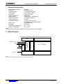
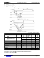
LMT050DNCFWU 50DNCFWU-N NCN LCD Module User Manual Prepared by: Checked by: Approved by: Date: Date: Yang Date: 2012-11-15 Rev. 0.1 URL: Descriptions Preliminary www.topwaydisplay.com www.topwaysz.com Release Date 2012-11-15 Document Name: LMT050DNCFWU LMT050DNCFWU-NCN-Manual-Rev0.1 Page: 1 of 11 TOPWAY LCD Module User Manual LMT050DNCFWU-NCN Table of Content 1. General Specification ............................................................................................................ 3 2. Block Diagram........................................................................................................................ 3 3. Terminal Functions................................................................................................................ 4 3.1 Interface ............................................................................................................................... 4 4. Absolute Maximum Ratings .................................................................................................. 5 5. Electrical Characteristics ...................................................................................................... 5 5.1 6. DC Characteristics (MCU terminal)....................................................................................... 5 AC Characteristics................................................................................................................. 6 6.1 TFT Controller Timing Characteristics .................................................................................. 6 6.2 TFT Controller Reset Timing ................................................................................................ 7 6.3 TFT Timing........................................................................................................................... 8 7. Optical Characteristics .......................................................................................................... 9 8. Precautions of using LCD Modules .................................................................................... 11 URL: www.topwaydisplay.com www.topwaysz.com Document Name: LMT050DNCFWU-NCN-Manual-Rev0.1 Page: 2 of 11 TOPWAY LCD Module User Manual LMT050DNCFWU-NCN 1. General Specification Screen Size(Diagonal) : Resolution : Signal Interface : Color Depth : Pixel Pitch : Pixel Configuration : Display Mode : Surface Treatment : Viewing Direction : Outline Dimension : 5.0 inch 800(RGB) x 480 8 bit parallel interface 65,535 color (16bit) *1 0.36 x 0.36 (mm) RGB Stripe Transmissive / normal white Anti-Glare Treatment 6 o’ clock 142.0 x 79.0 x 6.9 (mm) (see attached drawing for details) 108 x 64.8 (mm) 2x7 LEDs -20 ~ +70°C -30 ~ +80°C Active Area : Backlight : Operating Temperature : Storage Temperature : Note: *1 Color tune may slightly changed by temperature and driving voltage. 2. Block Diagram VDD, VSS Backlight Gate Driver /LE_HI LATCHES /RES,/WR, /CS, A0 D0~D7 TE TFT controller SSD1963 Backlight Driver Power Circuit 5.0”TFT Panel Source Driver Note: LATCHES on board expend the host 8bit data for SSD1963 16bit Interface. URL: www.topwaydisplay.com www.topwaysz.com Document Name: LMT050DNCFWU-NCN-Manual-Rev0.1 Page: 3 of 11 TOPWAY LCD Module User Manual LMT050DNCFWU-NCN 3. Terminal Functions 3.1 Interface No. Pin Name 1 VSS 2 3 VDD 4 5 A0 6 /CS 7 /RES 8 : 15 16 17 18 19 D0(D8) : D7(D15) TE NC /WR VSS 20 /LE_HI 21 : 26 NC I/O Descriptions P Power Supply GND (0V) P Positive Power Supply (5.0V) Register Select I A0=0, command A0=1, data or parameter I Chip Select signal Reset signal, I /RES=1, normal /RES=0, reset execute I 8bit Data bus O -I P Tear Signal (*1) No Connection Write signal Power Supply GND (0V) LATCH the high byte data; I /LE_HI=1, transparent; /LE_HI=0, LATCHED -- No Connection Note. *1. Tear signal may leave open when not use URL: www.topwaydisplay.com www.topwaysz.com Document Name: LMT050DNCFWU-NCN-Manual-Rev0.1 Page: 4 of 11 TOPWAY LCD Module User Manual LMT050DNCFWU-NCN 4. Absolute Maximum Ratings Items Supply Voltage Operating Temperature Storage Temperature Symbol VDD TOP TST Min. -0.3 -20 -30 Max. +6.0 +70 +80 Unit V C C Condition GND = 0V No Condensation No Condensation Cautions: Any Stresses exceeding the Absolute Maximum Ratings may cause substantial damage to the device. Functional operation of this device at other conditions beyond those listed in the specification is not implied and prolonged exposure to extreme conditions may affect device reliability. 5. Electrical Characteristics 5.1 DC Characteristics (MCU terminal) Items Operating Voltage Input High Voltage Input Low Voltage Output Signal Low Voltage Output Signal High Voltage Operating Current (*1) GND=0V, VDD =5.0V, TOP =25C Unit Applicable Pin Symbol MIN. TYP. MAX. VDD VIH VIL VOL VOH 4.8 3.0 GND 3.3 5.5 3.6 0.3 GND+0.4 - V V V V V IDD - 5.0 260 390 - mA VDD Input pins Input pins 60%PWM 100%PWM Note. *1. For different LCM, the value may have a bit of difference. *2. To test the current dissipation, use “all Black Pattern”. URL: www.topwaydisplay.com www.topwaysz.com Document Name: LMT050DNCFWU-NCN-Manual-Rev0.1 Page: 5 of 11 TOPWAY LCD Module User Manual LMT050DNCFWU-NCN 6. AC Characteristics 6.1 TFT Controller Timing Characteristics 8080 Mode Write Timing 8080 Mode Read Timing VSS=0V, VDD=5.0V, TOP=25C Item System Clock Period(*1) Control Pulse High Width Write Read Control Pulse Low Width Write (next write cycle) Write (next read cycle) Read Address Setup Time Address Hold Time Write Data Setup Time Write Data Hold Time Write Low Time Read Data Hold Time Access Time Read Low Time Rise Time Fall Time Chip select setup time Chip select hold time to read signal Symbol tMCLK tPWCSL tPWCSH tAS tAH tDSW tDHW tPWLW tDHR tACC tPWLR tR tF tCS tCSH MIN. 1/fMCLK TYP. - MAX. - Unit ns 16 1.5*tMCLK - ns 38 1.3*tMCLK - ns 16 1.5*tMCLK - ns 100 100 1.3 2.5 5 1.3 15 1.3 40 45 2.5 4 9*tMCLK 9*tMCLK - 0.4 0.4 - ns ns ns ns ns ns ns ns ns ns ns ns ns ns Note: *1. tMCLK is the System Clock Period, which may config by internal PLL setting *2. This Module is driving by 10MHz Xtal, Xtal and clock up by enabling the SSD1963 internal PLL *3. Suggested PLL clock setting is 200MHz URL: www.topwaydisplay.com www.topwaysz.com Document Name: LMT050DNCFWU LMT050DNCFWU-NCN-Manual-Rev0.1 Page: 6 of 11 TOPWAY 6.2 LMT050DNCFWU-NCN TFT Controller Reset Timing Item Reset setup time Reset pulse Reset hold time URL: LCD Module User Manual www.topwaydisplay.com www.topwaysz.com Symbol trs trst trh MIN. 2 0.2 2 VSS=0V, VDD=3.3V, TOP=25C TYP. MAX. Unit ms ms ms Document Name: LMT050DNCFWU LMT050DNCFWU-NCN-Manual-Rev0.1 Page: 7 of 11 TOPWAY 6.3 LCD Module User Manual LMT050DNCFWU-NCN TFT Timing Item Symbol MIN. TYP. MAX. Unit Horizontal Display Area thd CLKIN Frequency fclk - 30 50 MHz th 889 928 1143 CLKIN thpw 1 48 255 CLKIN One Horizontal Line HSD pulse width 800 DCLK HSD Blanking thb HSD Front Porch thfp Vertical Display Area tvd VSD period time tv 513 525 767 TH VSD pulse width tvpw 3 3 255 TH VSD Blanking tvb VSD Front Porch tvfp 88 1 40 CLKIN 255 480 13 CLKIN TH 32 1 Remark TH 255 TH Horizontal timing diagram Vertical timing diagram URL: www.topwaydisplay.com www.topwaysz.com Document Name: LMT050DNCFWU LMT050DNCFWU-NCN-Manual-Rev0.1 Page: 8 of 11 TOPWAY LCD Module User Manual LMT050DNCFWU-NCN 7. Optical Characteristics Item Symbol Condition MIN. TYP. MAX. 40 50 - 60 70 - 60 70 - 60 70 - θ=0 500 600 - 25℃ - 20 30 X 0.260 0.310 0.360 Y 0.280 0.330 0.380 0.540 0.590 0.640 0.300 0.350 0.400 0.298 0.348 0.398 Y 0.520 0.570 0.620 X 0.095 0.145 0.195 Y 0.060 0.110 0.160 L - 135 - - 50 75 80 θT θB Viewing angle θL (CR≥10) θR Contrast ratio CR Ton Response Time Toff White Red Chromaticlty Green Blue Luminance o X Y X Backlight is on NTSC Luminance uniformity U - UNIT Note. degree Note 2 - Note 1,3 msec msec Note 1,4 Note 1,5 cd/m 2 Note 1,6 % Note 5 % Note 1,7 Test Conditions: 1. IF= 160 mA, VF=9.6V, and the ambient temperature is 25. ℃ 2. The test systems refer to Note 1 and Note 2. URL: www.topwaydisplay.com www.topwaysz.com Document Name: LMT050DNCFWU-NCN-Manual-Rev0.1 Page: 9 of 11 TOPWAY LCD Module User Manual Note 1: The data are measured after LEDs are turned on for 5 minutes. LCM displays full white. The brightness is the average value of 9 measured spots. Measurement equipment SR-3A SR (1°) Measuring condition: - Measuring surroundings: Dark room - Measuring temperature: Ta=25℃ ℃. - Adjust operating voltage to get optimum contrast at the center of the display. Note 3: The definition of contrast ratio (Test LCM using SR-3A SR (1°)): Luminance When LCD is at “White”state Contrast = Ratio(CR) Luminance When LCD is at “Black”state (Contrast Ratio is measured in optimum common electrode voltage) Note 5: Definition of Color of CIE1931 Coordinate and NTSC Ratio. Color gamut: Area of RGB triangle S= Area of NTSC triangle X100% LMT050DNCFWU-NCN Note 2: The definition of viewing angle: Refer to the graph below marked by θ and Ф Note 4: Definition of Response time. (Test LCD using BM BM-7A(2°)): The output signals of photo detector are measured when the input signals are changed from “black”to “white”(falling time) and from “white”to “black”(rising time), respectively. The response time is defined as the time interval between the 10% and 90% of amplitudes.Refer to figure as below. Note 6: The luminance uniformity is calculated by using following formula. △Bp Bp = Bp (Min.) / Bp (Max.)×100 (%) Bp (Max.) = Maximum brightness in 9 measured spots Bp (Min.) = Minimum brightness in 9 measured spots . Note 7: Measured the luminance of white state at center point URL: www.topwaydisplay.com www.topwaysz.com Document Name: LMT050DNCFWU LMT050DNCFWU-NCN-Manual-Rev0.1 Page: 10 of 11 TOPWAY LCD Module User Manual LMT050DNCFWU-NCN 8. Precautions of using LCD Modules Mounting - Mounting must use holes arranged in four corners or four sides. - The mounting structure so provide even force on to LCD module. Uneven force (ex. Twisted stress) should not applied to the module. And the case on which a module is mounted should have sufficient strength so that external force is not transmitted directly to the module. - It is suggested to attach a transparent protective plate to the surface in order to protect the polarizer. It should have sufficient strength in order to the resist external force. - The housing should adopt radiation structure to satisfy the temperature specification. - Acetic acid type and chlorine type materials for the cover case are not desirable because the former generates corrosive gas of attacking the polarizer at high temperature and the latter causes circuit break by electro-chemical reaction. - Do not touch, push or rub the exposed polarizers with glass, tweezers or anything harder than HB pencil lead. Never rub with dust clothes with chemical treatment. Do not touch the surface of polarizer for bare hand or greasy cloth.(Some cosmetics deteriorate the polarizer.) - When the surface becomes dusty, please wipe gently with absorbent cotton or other soft materials like chamois soaks with petroleum benzine. Normal-hexane is recommended for cleaning the adhesives used to attach front / rear polarizers. Do not use acetone, toluene and alcohol because they cause chemical damage to the polarizer. - Wipe off saliva or water drops as soon as possible. Their long time contact with polarizer Operating - The spike noise causes the mis-operation of circuits. It should be within the ± 200mV level (Over and under shoot voltage) - Response time depends on the temperature.(In lower temperature, it becomes longer.) - Brightness depends on the temperature. (In lower temperature, it becomes lower.) And in lower temperature, response time(required time that brightness is stable after turned on) becomes longer. - Be careful for condensation at sudden temperature change. Condensation makes damage to polarizer or electrical contacted parts. And after fading condensation, smear or spot will occur. - When fixed patterns are displayed for a long time, remnant image is likely to occur. - Module has high frequency circuits. Sufficient suppression to the electromagnetic interference shall be done by system manufacturers. Grounding and shielding methods may be important to minimized the interference Electrostatic Discharge Control Since a module is composed of electronic circuits, it is not strong to electrostatic discharge. Make certain that treatment persons are connected to ground through wrist band etc. And don’ t touch interface pin directly. Strong Light Exposure Strong light exposure causes degradation of polarizer and color filter. Storage When storing modules as spares for a long time, the following precautions are necessary. - Store them in a dark place. Do not expose the module to sunlight or fluorescent light. Keep the temperature between 5°C and 35°C at normal humidity. - The polarizer surface should not come in contact with any other object. It is recommended that they be stored in the container in which they were shipped. Protection Film - When the protection film is peeled off, static electricity is generated between the film and polarizer. This should be peeled off slowly and carefully by people who are electrically grounded and with well ion-blown equipment or in such a condition, etc. - The protection film is attached to the polarizer with a small amount of glue. If some stress is applied to rub the protection film against the polarizer during the time you peel off the film, the glue is apt tore main on the polarizer. Please carefully peel off the protection film without rubbing it against the polarizer. - When the module with protection film attached is stored for a long time, sometimes there remains a very small amount of glue still on the polarizer after the protection film is peeled off. - You can remove the glue easily. When the glue remains on the polarizer surface or its vestige is recognized, please wipe them off with absorbent cotton waste or other soft material like chamois soaked with normal-hexane. Transportation The LCD modules should be no falling and violent shocking during transportation, and also should avoid excessive press, water, damp and sunshine. URL: www.topwaydisplay.com www.topwaysz.com Document Name: LMT050DNCFWU-NCN-Manual-Rev0.1 Page: 11 of 11