1
Application Note
V850ES/Jx3-L
Sample Program (Watchdog Timer 2 (WDT2))
Reset Generated by Infinite Loop Detection
This document summarizes the operations of the sample program and describes how to use the sample program and
how to set and use watchdog timer 2. In the sample program, an interrupt is generated by detecting the falling edge of
the switch input. If no WDT2 overflow occurs, LED1 blinks in a cycle of approximately 55 ms while SW1 is turned on.
After SW1 is turned off, LED1 blinks in a cycle of approximately 120 ms. If a WDT2 overflow occurs, a reset signal is
generated by WDT2. After the reset is released, LED2 is turned on and LED1 blinks in a cycle of approximately 120 ms.
Target devices
V850ES/JF3-L microcontroller
V850ES/JG3-L microcontroller
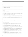
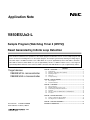
CONTENTS
CHAPTER 1 OVERVIEW.......................................................................................... 3
1.1
Initial Settings ................................................................................................ 4
1.2
Operation of Watchdog Timer 2 (WDT2)........................................................ 5
1.3
Enabling Interrupts......................................................................................... 5
1.4
Main Loop ...................................................................................................... 5
1.5
Interrupt Servicing.......................................................................................... 6
CHAPTER 2 CIRCUIT DIAGRAM.............................................................................. 7
2.1
Circuit Diagram .............................................................................................. 7
2.2
Peripheral Hardware ...................................................................................... 7
CHAPTER 3 SOFTWARE......................................................................................... 8
3.1
File Configuration........................................................................................... 8
3.2
On-Chip Peripheral Functions Used............................................................... 9
3.3
Initial Settings and Operation Overview ......................................................... 9
3.4
Flowchart ..................................................................................................... 11
3.5
Differences Between V850ES/JG3-L and V850ES/JF3-L ............................ 13
3.6
Security ID ................................................................................................... 13
CHAPTER 4 SETTING REGISTERS ...................................................................... 14
4.1
Settings of Watchdog Timer 2 (WDT2) ........................................................ 15
4.2
Checking Detection of WDT2 Reset............................................................. 20
CHAPTER 5 RELATED DOCUMENTS ................................................................. 21
Document No. U19543EJ1V0AN00
Date Published February 2009 N
2008
Printed in Japan
APPENDIX A PROGRAM LIST ................................................................................ 22
• The information in this document is current as of November, 2008. The information is subject to
change without notice. For actual design-in, refer to the latest publications of NEC Electronics data
sheets or data books, etc., for the most up-to-date specifications of NEC Electronics products. Not
all products and/or types are available in every country. Please check with an NEC Electronics sales
representative for availability and additional information.
• No part of this document may be copied or reproduced in any form or by any means without the prior
written consent of NEC Electronics. NEC Electronics assumes no responsibility for any errors that may
appear in this document.
• NEC Electronics does not assume any liability for infringement of patents, copyrights or other intellectual
property rights of third parties by or arising from the use of NEC Electronics products listed in this document
or any other liability arising from the use of such products. No license, express, implied or otherwise, is
granted under any patents, copyrights or other intellectual property rights of NEC Electronics or others.
• Descriptions of circuits, software and other related information in this document are provided for illustrative
purposes in semiconductor product operation and application examples. The incorporation of these
circuits, software and information in the design of a customer's equipment shall be done under the full
responsibility of the customer. NEC Electronics assumes no responsibility for any losses incurred by
customers or third parties arising from the use of these circuits, software and information.
• While NEC Electronics endeavors to enhance the quality, reliability and safety of NEC Electronics products,
customers agree and acknowledge that the possibility of defects thereof cannot be eliminated entirely. To
minimize risks of damage to property or injury (including death) to persons arising from defects in NEC
Electronics products, customers must incorporate sufficient safety measures in their design, such as
redundancy, fire-containment and anti-failure features.
• NEC Electronics products are classified into the following three quality grades: "Standard", "Special" and
"Specific".
The "Specific" quality grade applies only to NEC Electronics products developed based on a customerdesignated "quality assurance program" for a specific application. The recommended applications of an NEC
Electronics product depend on its quality grade, as indicated below. Customers must check the quality grade of
each NEC Electronics product before using it in a particular application.
"Standard": Computers, office equipment, communications equipment, test and measurement equipment, audio
and visual equipment, home electronic appliances, machine tools, personal electronic equipment
and industrial robots.
"Special": Transportation equipment (automobiles, trains, ships, etc.), traffic control systems, anti-disaster
systems, anti-crime systems, safety equipment and medical equipment (not specifically designed
for life support).
"Specific": Aircraft, aerospace equipment, submersible repeaters, nuclear reactor control systems, life
support systems and medical equipment for life support, etc.
The quality grade of NEC Electronics products is "Standard" unless otherwise expressly specified in NEC
Electronics data sheets or data books, etc. If customers wish to use NEC Electronics products in applications
not intended by NEC Electronics, they must contact an NEC Electronics sales representative in advance to
determine NEC Electronics' willingness to support a given application.
(Note)
(1) "NEC Electronics" as used in this statement means NEC Electronics Corporation and also includes its
majority-owned subsidiaries.
(2) "NEC Electronics products" means any product developed or manufactured by or for NEC Electronics (as
defined above).
M8E 02. 11-1
2
Application Note U19543EJ1V0AN
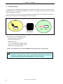
CHAPTER 1 OVERVIEW
This sample program describes the usage of watchdog timer 2 (WDT2).
The overflow time of WDT2 is specified as 125 ms based on the subclock. When an overflow occurs, an internal
reset signal (WDT2RES) is generated.
After initial setup is complete, an interrupt is generated and serviced when the falling edge of the switch input is
detected. LED1 blinks and the WDT2 counter is cleared in a cycle of 55 ms while the switch is being pressed. When
a reset is generated by WDT2, the initial settings specify that LED2 turns on.
The settings for peripheral functions that remain stopped after reset is released and that are not used in this
sample program have not been specified.
The main software operations are shown below.
WDT2 reset occurs.
Non-WDT2 reset occurs.
1.1 Initial Settings
Clocks, Bus waits
1.2 Operation of Watchdog Timer 2 (WDT2)
Setting up ports and
alternate functions
LED2 turns on.
LED2 turns off.
1.3 Enabling Interrupts
1.4 Main Loop
Application Note U19543EJ1V0AN
1.5 Interrupt Servicing
3
CHAPTER 1 OVERVIEW
1.1
Initial Settings
<Referencing option byte>
• Referencing the oscillation stabilization time after releasing reset
<Settings of on-chip peripheral functions>
• Setting wait operations <wait: 1> for bus access to on-chip peripheral I/O registers
• Setting on-chip debug mode <normal operation mode>
• Stopping the internal oscillator, setting watchdog timer 2 mode <reset mode>
• Setting the use of the subclock and setting the internal system clock
• Setting to PLL mode and setting to 20 MHz operation (5 MHz × 4).
<Pin settings>
• Setting unused pins
• Setting external interrupt pins (edge specification, priority specification, unmasking)
• Setting LED output pins
<Settings of 16-bit interval timer M (TMM)>
• Selecting the count clock (fXX/512)
• Setting the TMM count
• Masking interrupts from timer M
• Enabling operation of TMM
4
Application Note U19543EJ1V0AN
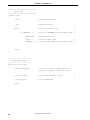
CHAPTER 1 OVERVIEW
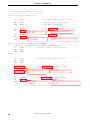
1.2
Operation of Watchdog Timer 2 (WDT2)
Watchdog timer 2 generates an internal reset signal (WDT2RES) when an overflow occurs.
When a WDT2 reset occurs, LED2 turns on and LED1 blinks about every 120 ms.
When a reset other than a WDT2 reset occurs, LED2 turns off and LED1 blinks about every 120 ms.
WDT2 reset
WDT2 reset WDT2 reset
occurred released
Output
WDT2 overflow
threshold
LED1
LED2
Output
Blinks about
every 120 ms.
125 ms
WDT2 count
LED1
Turns on.
LED2
Reset other than WDT2 reset
Output
Blinks about
every 120 ms.
Reset occurrence
LED1
1.3
Turns off.
Reset release
LED2
Enabling Interrupts
• Enabling interrupts by using the EI instruction
1.4
Main Loop
• Executing an infinite loop (LED1 blinks about every 120 ms while the system is waiting for an interrupt generated
by switch input.)
Application Note U19543EJ1V0AN
5
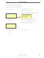
CHAPTER 1 OVERVIEW
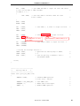
1.5
Interrupt Servicing
Interrupts are serviced by detecting the falling edge of the INTP0 pin, caused by switch input. In interrupt servicing,
the LED1 blinking cycle is changed by confirming that the switch is on, after about 10 ms have elapsed after the falling
edge of the INTP0 pin was detected.
The switch being off, after about 10 ms have elapsed after the falling edge of the INTP0 pin was detected, is
identified as chattering noise and the LED1 blinking cycle is not changed.
<Output>
<Input>
ON
LED1
SW1
LED2
V850ES/Jx3-L
microcontroller
The reset source is confirmed (RESF = 0x00).
→ LED1 blinks (120 ms), LED2 turns off.
→ A switch input interrupt occurs.
→ LED1 blinks (55 ms).
→ A reset occurs triggered by a WDT2 overflow.
→ The reset source is confirmed (RESF = 0x10).
→ LED2 turns on, LED1 blinks (120 ms)
Caution
See each product user’s manual (V850ES/Jx3-L) for cautions when using the device.
[Column] What is chattering?
Chattering is a phenomenon that an electric signal alternates between being on and off when
a connection flip-flops mechanically immediately after a switch is switched.
6
Application Note U19543EJ1V0AN
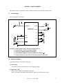
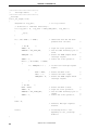
CHAPTER 2 CIRCUIT DIAGRAM
This chapter describes a circuit diagram and the peripheral hardware to be used in this sample program.
2.1
Circuit Diagram
The circuit diagram is shown below.
VDD VDD
VDD
VDD
SW1
INTP0 (P03)
V850ES/Jx3-L
microcontroller
LED2
PCM2
VDD
LED1
PCM3
X1
REGC
X2
VDD
FLMD0
RESET
XT1
XT2
VSS
Cautions 1. Connect the EVDD, AVREF0, and AVREF1 pins directly to VDD.
2. Connect the EVSS and AVSS pins directly to GND.
3. Connect the FLMD0 pin to GND in normal mode.
4. Connect REGC to GND via a capacitor (recommended value: 4.7 μF).
5. Leave all unused ports open, because they will be handled as output ports.
2.2
Peripheral Hardware
The peripheral hardware to be used is shown below.
(1) Switch (SW1)
This switch is used as an interrupt input to control the lighting of LED1.
(2) LEDs (LED1, LED2)
LED1 is used as outputs corresponding to switch inputs.
When a reset signal is generated by watchdog timer 2, LED2 turns on following reset release.
Application Note U19543EJ1V0AN
7
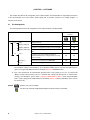
CHAPTER 3 SOFTWARE
This chapter describes the file configuration of the compressed files to be downloaded, on-chip peripheral functions
of the microcontroller to be used, and the initial settings and an operation overview of the sample program. A
flowchart is also shown.
3.1
File Configuration
The following table shows the file configuration of the compressed files to be downloaded.
File Name (Tree Structure)
c
conf
crtE.s
Description
Compressed (*.zip) Files
Included
Note 1
Startup routine file
z
Link directive file
z
z
AppNote_WDT2.prj
Project file for integrated development environment PM+
−
z
AppNote_WDT2.prw
Workspace file for integrated development environment
−
z
hardware initialization processing and main processing
of microcontroller
z
z
minicube2.s
Source file for reserving area for MINICUBE2
z
z
opt_b.s
Source file for setting option byte
z
z
PM+
src
−
AppNote_WDT2.dir
Note 2
main.c
C language source file including descriptions of
Notes 1. This is the startup file copied when “Copy sample for use (C)” is selected when “Specify startup file” is
selected when creating a new workspace. (If the default installation path is used, the startup file will be a
copy of C:\Program Files\NEC Electronics Tools\PM+\Version used\lib850\r32\crtE.s.)
2. This is the link directive file automatically generated when “Copy sample for use (C)” is selected and
“Memory usage: Internal memory only (I)” is checked when “Specify link directive file” is selected when
creating a new workspace, and to which a segment for MINICUBE2 is added. (If the default installation
path is used, C:\Program Files\NEC Electronics Tools\PM+\Version used\bin\w_data\V850_i.dat is used as
the reference file.)
Remark
: Only the source file is included.
: The files to be used with integrated development environment PM+ are included.
8
Application Note U19543EJ1V0AN
CHAPTER 3 SOFTWARE
3.2
On-Chip Peripheral Functions Used
The following on-chip peripheral functions of the microcontroller are used in this sample program.
• Watchdog timer 2 (used to generate an overflow):
WDT2
• 16-bit interval timer M (used to generate the LED blinking cycle): TMM
• External interrupt input (for switch input):
INTP0 (SW1)
• Output ports (for lighting LEDs):
PCM2 (LED2), PCM3 (LED1)
3.3
Initial Settings and Operation Overview
In this sample program, the selection of the clock frequency, setting of WDT2, setting of the I/O ports and external
interrupt pins, setting of a TMM count clock, setting of interrupts, and ROMization processing are performed in the
initial settings.
After initial setup is complete, LED1 blinks about every 120 ms, and interrupts are generated and serviced upon
detection of the falling edge of the switch input (SW1). If no WDT2 overflow occurs during interrupt servicing, LED1
blinks about every 55 ms while SW1 is turned on. When SW1 is turned off, LED1 blinks about every 120 ms. If a
WDT2 overflow occurs during interrupt servicing, watchdog timer 2 generates a reset signal. After the reset is
released, LED2 turns on and LED1 blinks about every 120 ms.
The details are described in the state transition diagram shown below.
Application Note U19543EJ1V0AN
9
CHAPTER 3 SOFTWARE
Non-WDT2 reset
WDT2 reset
Initial settings
z Referencing the option byte
• Referencing the oscillation stabilization time after releasing
reset
z Settings of on-chip peripheral functions
• Setting a bus wait for on-chip peripheral I/O registers
• Setting on-chip debugging to normal operation mode
• Stopping the internal oscillator
• Setting watchdog timer 2 to reset mode
• Setting the subclock and internal system clock, and setting the
PLL mode
z Pin settings
• Setting unused pins
• Setting the external interrupt pins (switch input)
• Setting the output pins (LED control)
• Both LED1 and LED2 are turned off.
• LED2 is turned on when a reset triggered by WDT2 occurs.
z Setting timer M
• Selecting fXX/512 as the count clock
• Setting the TMM count
• Masking interrupts from timer M
• Enabling operation of TMM
z Enabling interrupts
Interrupt input is awaited.
No interrupt
LED1 blinks every 120 ms
Infinite loop
Interrupt servicing is
terminated when switch
input turns off.
The falling edge of INTP0
PUSH
is detected.
10 ms chattering is detected.
INTP0 pin = High level
An interrupt is
generated.
The blinking
cycle is
changed.
An interrupt is generated by switch input.
10
Application Note U19543EJ1V0AN
LED1 is blinking in a
cycle of 55 ms.
CHAPTER 3 SOFTWARE
3.4
Flowchart
A flowchart for the sample program is shown below.
• Main processing flow
Start
The option byte is referencedNote
Startup routine processing
Startup
(using a sample)
The clock, bus waits,
and watchdog timer are initialized
Unused ports are initialized
Initialization
The ports used, including interrupts,
are initialized
Timer M is initialized
Enabling
interrupts
Interrupts enabled (EI)
TMM = 120 ms ?
(TM0EQIF0 = 1)
NO
YES
WDT2 is cleared
The LED1 output is inverted
The TMM compare match interrupt
request is cleared
(TM0EQIF0 = 0)
Note The option byte is automatically referenced by the microcontroller after reset is released. In this sample
program, the oscillation stabilization time after releasing reset is set to 6.554 ms with the option byte.
Application Note U19543EJ1V0AN
11
CHAPTER 3 SOFTWARE
• Interrupt servicing flow
INTP0
10 ms wait
No
SW1 = ON?
YES
TMM operation disabled
TM0CE = 0
TMM compare register set to 55 ms
(TM0CMP0 = 55 ms)
TMM compare match interrupt
request cleared
(TM0EQIF0 = 0)
TMM operation enabled
TM0CE = 1
No
SW1 = OFF?
Yes
WDT2 cleared
TMM = 55 ms?
(TM0EQIF0 = 1)
TMM operation disabled
Yes
(TM0CE = 0)
WDT2 cleared
TMM compare register set to 120 ms
(TM0CMP0 = 120 ms)
LED1 output inverted
TMM operation enabled
TMM compare match interrupt
request cleared
(TM0EQIF0 = 0)
TM0CE = 1
INTP0 interrupt request cleared
PIF0 = 0
RETI
12
Application Note U19543EJ1V0AN
No
CHAPTER 3 SOFTWARE
[Column] Contents of the startup routine
The startup routine is a routine that is executed before executing the main function after reset of the V850 is
released. Basically, the startup routine executes initialization so that the program written in C language can
start operating.
Specifically, the following are performed.
• Securing the argument area of the main function
• Securing the stack area
• Setting the RESET handler when reset is issued
• Setting the text pointer (tp)
• Setting the global pointer (gp)
• Setting the stack pointer (sp)
• Setting the element pointer (ep)
• Setting mask values to the mask registers (r20 and r21)
• Clearing the sbss and bss areas to 0
• Setting the CTBP value for the prologue epilogue runtime library of the function
• Setting r6 and r7 as arguments of the main function
• Branching to the main function
3.5
Differences Between V850ES/JG3-L and V850ES/JF3-L
The V850ES/JG3-L is the V850ES/JF3-L with its functions, such as I/Os, timer/counters, and serial interfaces,
expanded.
In this sample program, the initialization range of P1, P3, P7, P9, and PDH in I/O initialization differs.
See APPENDIX A PROGRAM LIST for details of the sample program.
3.6
Security ID
The content of the flash memory can be protected from unauthorized reading by using a 10-byte ID code for
authorization when executing on-chip debugging using an on-chip debug emulator.
For details of ID security, see the V850ES/Jx3-L Sample Program (Interrupt) External Interrupt Generated by
Switch Input Application Note.
Application Note U19543EJ1V0AN
13
CHAPTER 4 SETTING REGISTERS
This chapter describes the watchdog timer 2 (WDT2) settings.
For other initial settings, refer to the V850ES/Jx3-L Sample Program (Initial Settings) LED Lighting Switch
Control Application Note. For interrupt, refer to the V850ES/Jx3-L Sample Program (Interrupt) External Interrupt
Generated by Switch Input Application Note.
Among the peripheral functions that are stopped after reset is released, those that are not used in this sample
program are not set.
For how to set registers, see each product user’s manual.
• V850ES/JG3-L 32-bit Single-Chip Microcontroller
Hardware User’s Manual
• V850ES/JF3-L 32-bit Single-Chip Microcontroller
Hardware User’s Manual
See the following user’s manuals for details of extended descriptions in C and assembly languages.
• CA850 C Compiler Package C Language User’s Manual
• CA850 C Compiler Package Assembly Language User’s Manual
14
Application Note U19543EJ1V0AN
CHAPTER 4 SETTING REGISTERS
4.1
Settings of Watchdog Timer 2 (WDT2)
Watchdog timer 2 operates in the following two modes:
• A mode in which WDT2 is used as a reset trigger
• A mode in which WDT2 is used as an interrupt trigger
Watchdog timer 2 is mainly controlled by the following two registers:
• Watchdog timer mode register 2 (WDTM2)
• Watchdog timer enable register (WDTE)
4.1.1
Watchdog timer mode register 2 (WDTM2)
Watchdog timer mode register 2 (WDTM2) is used to set the overflow time and operating clock of watchdog timer 2.
WDTM2 can be read and written in 8-bit units. This register can be read any number of times, but it can be written
only once following reset release.
Reset sets this register to 0x67.
Caution
Accessing the WDTM2 register is prohibited in the following statuses.
• When the CPU is operating on the subclock and main clock oscillation is stopped.
• When the CPU is operating on the internal oscillation clock.
Figure 4-1. Format of WDTM2 Register
Watchdog timer mode register 2 (WDTM2)
Address: 0xFFFF6D0
7
6
5
4
3
2
1
0
0
WDM21
WDM20
WDCS24
WDCS23
WDCS22
WDCS21
WDCS20
WDM21
WDM20
0
0
0
1
×
Selection of watchdog timer 2 operation mode
Operation stopped
1
Non-maskable interrupt request mode (WDT2 generates the INTWDT2 signal)
Note
Reset mode (WDT2 generates the WDT2RES signal)
WDCS24 WDCS23 WDCS22 WDCS21 WDCS20
1
×
Note
0
1
Selection of watchdog timer 2 clock
1
212/fXT (125 ms)
Note Either 0 or 1
Remark
• The red values in the table indicate the values set in the sample program (WDTM2 = 0x5B).
• fXT = 32.768 kHz
Application Note U19543EJ1V0AN
15
CHAPTER 4 SETTING REGISTERS
4.1.2
Watchdog timer enable register (WDTE)
Writing 0xAC to the WDTE register clears the counter of watchdog timer 2 and causes the counter to start counting
up again.
This register can be read and written in 8-bit units. Writing WDTE using a 1-bit memory manipulation instruction
will cause an overflow to occur.
Reset sets this register to 0x9A.
Figure 4-2. Format of WDTE Register
Watchdog timer enable register (WDTE)
Address: 0xFFFFF6D1
7
6
5
4
3
2
1
0
Cautions 1. Writing a value other than 0xAC to the WDTE register will trigger forcible generation of the
overflow signal.
2. To deliberately trigger generation of the overflow signal, write a value other than 0xAC to
the WDTE register once, or write to the WDTM2 register twice.
Note, however, that if
operation of watchdog timer 2 has been stopped, writing a value other than 0xAC to the
WDTE register once or writing to the WDTM2 register twice will not trigger generation of the
overflow signal.
3. The value read from the WDTE register is 0x9A (which differs from the value written—0xAC).
16
Application Note U19543EJ1V0AN
CHAPTER 4 SETTING REGISTERS
• Using the detection of a watchdog timer 2 overflow as a trigger to generate a reset
(Same contents as sample program)
• Setup procedure
Set WDTM2 to 0x5B (in the program example, this sets reset mode and an operating clock of 212/fXT (125 ms)).
Set WDTE to 0xAC before the overflow detection time elapses (clearing the watchdog timer 2 count value) to
stop the occurrence of a reset. If the watchdog timer 2 count value is not cleared before the overflow detection
time elapses, a reset will occur.
In the program example, the operating clock is set to 212/fXT, so the overflow detection time of watchdog timer 2
is 125 ms.
• Program example (same contents as sample program)
#define VAL_120ms_CNT
(4688)
/* Cycle in which WDT2 count is cleared (120 ms)
*/
Section of initialization processing
Initialization processing for other than WDT2 is omitted here
/* Using detection of WDT2 overflow as a reset trigger */
WDTM2 = 0x5B;
/* Starts watchdog timer 2 operation
*/
<1>
Section of main processing
Main processing for other than WDT2 is omitted here
WDTE = 0xAC;
/* Clears WDT2 count
Application Note U19543EJ1V0AN
*/
<2>
17
CHAPTER 4 SETTING REGISTERS
• Using the detection of a watchdog timer 2 overflow as a trigger to generate an interrupt
The overflow of watchdog timer 2 is likely to cause the CPU to enter an infinite processing loop. It is therefore
recommended to set watchdog timer 2 to the reset mode (by setting the WDM21 bit to 1) so that the CPU is reset
when WDT2 overflows.
If you choose to set watchdog timer 2 to non-maskable interrupt request mode (by setting the WDM21 bit to 0
and the WDM20 bit to 1), however, be sure to stop the system after the system error processing has been
completed by the INTWDT2 interrupt servicing routine. The system cannot be returned to the main processing
routine by using the RETI instruction after the servicing of a non-maskable interrupt generated by the INTWDT2
signal has finished. To return the system to the main processing routine following the servicing of an INTWDT2
interrupt, execute the software reset processing shown below.
Note that in this software reset processing, registers that can be set only once following the release of reset
(such as the WDTM2 register) cannot be set again. These registers must be initialized by executing a hardware
reset by means such as inputting a signal to the reset pin.
INTWDT2 is generated
Software reset processing address set to FEPC
Value that sets NP bit to 1 and EP bit to 0 set to FEPSW
↓
INTWDT2 servicing
routine
RETI
RETI executed 10 times (FEPC, EIPC, FEPSW and
EIPSW
Note
settings required)
↓
Software reset processing
routine
Initialization processing
Note A value that sets the NP bit to 0, the EP bit to 0, and the ID bit to 1
is set to FEPSW.
A value that sets the NP bit to 0, the EP bit to 0, and the ID bit to 1
is set to EIPSW.
18
Application Note U19543EJ1V0AN
CHAPTER 4 SETTING REGISTERS
• Example of program
#**********************************************#
#
Interrupt initialization processing
#
#**********************************************#
.global _initint
_initint:
mov
initloop1,r6
-- Sets the processing routine address
ldsr
r6,2
-- Set to FEPC
mov
0xa0,r6
-- NP=1, EP=0
ldsr
r6,3
-- Set to FEPSW
reti
-- Processing restored from NMI and returned to initloop1
initloop1:
mov
0x20,r6
-- PSW.NP set to 0 by next RETI instruction
ldsr
r6,3
-- Set to FEPSW
ldsr
r6,1
-- Set to EIPSW
mov
initloop2,r6
-- Sets processing routine address 2
ldsr
r6,2
-- Set to FEPC
ldsr
r6,0
-- Set to EIPC
mov
0x0b,r6
-- Count initial value (10 times)
sub
1,r6
-- Loop count (-1)
bz
initend
-- End of interrupt initialization
reti
initloop2:
reti
initend:
Application Note U19543EJ1V0AN
19
CHAPTER 4 SETTING REGISTERS
4.2
Checking Detection of WDT2 Reset
When a WDT2 reset occurs, the WDT2RF bit of the reset source flag register (RESF) is set. On the other hand,
when a reset is generated by an input to the RESET pin, the WDT2RF bit is cleared. Therefore, by checking the
WDT2RF bit after the reset is released, it is possible to ascertain whether the reset source was an WDT2 reset or an
input to the RESET pin.
4.2.1
Reset source flag register (RESF)
The RESF register stores information on which reset signal—the reset signal from which source—generated a
reset.
This register can be read or written in 8-bit or 1-bit units.
Note, however, that the RESF register can only be written using a combination of specific sequences.
A reset generated by an input to the RESET pin sets this register to 0x00. A reset generated by any other source,
such as watchdog timer 2 (WDT2), the low-voltage detector (LVI), or the clock monitor (CLM), sets the flag of the
corresponding source (WDT2RF, CLMRF, LVIRF bits); the other source flags hold their previous values.
Figure 4-3. Format of RESF Register
Reset source flag register (RESF)
Address: 0xFFFFF888
7
6
5
4
3
2
1
0
0
0
0
WDT2RF
0
0
CLMRF
LVIRF
WDT2RF
Occurrence of reset signal from WDT2
0
Did not occur
1
Occurred
CLMRF
Occurrence of reset signal from CLM
0
Did not occur
1
Occurred
LVIRF
Occurrence of reset signal from LVI
0
Did not occur
1
Occurred
Notes 1. Only 0 can be written to each bit. If writing 0 conflicts with the flag being set (due to the occurrence of a
reset), flag setting takes precedence.
2. If watchdog timer 2 (WDT2), the low-voltage detector (LVI), and the clock monitor (CLM) are being used
at the same time, the relevant reset source flag must be cleared after checking the reset source.
Remark
The blue values indicate the bits to be checked in the sample program.
[Clearing the reset source flag]
As mentioned in Note 2 on the previous page, there are cases when the reset source flag has to be cleared after
checking the reset source. In this sample program, however, the reset source flag does not have to be cleared
because only the watchdog timer 2 (WDT2) is used.
20
Application Note U19543EJ1V0AN
CHAPTER 5 RELATED DOCUMENTS
Document
English
V850ES/JF3-L Hardware User’s Manual
PDF
V850ES/JG3-L Hardware User’s Manual
PDF
PM+ Ver.6.30 User’s Manual
PDF
CA850 Ver.3.20 C Compiler Package Operation User’s Manual
PDF
CA850 Ver.3.20 C Compiler Package C Language User’s Manual
PDF
CA850 Ver.3.20 C Compiler Package Assembly Language User’s Manual
PDF
CA850 Ver.3.20 C Compiler Package Link Directive User’s Manual
PDF
V850ES Architecture User’s Manual
PDF
QB-MINI2 On-Chip Debug Emulator with Programming Function User’s Manual
PDF
ID850QB Ver. 3.40 Integrated Debugger Operation User’s Manual
PDF
Application Note U19543EJ1V0AN
21
APPENDIX A PROGRAM LIST
The V850ES/Jx3-L microcontroller source program is shown below as a program list example.
z opt_b.s
#-----------------------------------------------------------------------------#
#
NEC Electronics
V850ES/Jx3-L microcontroller
#
#-----------------------------------------------------------------------------#
V850ES/JG3-L JF3-L
JF3-L sample program
#-----------------------------------------------------------------------------#
Reset Generation When Infinite Loop Detected
#-----------------------------------------------------------------------------#[History]
#
2008.11.--
Released
#-----------------------------------------------------------------------------#[Overview]
#
This sample program sets the option byte.
#------------------------------------------------------------------------------
.section "OPTION_BYTES"
.byte 0b00000101 -- 0x7a (5 MHz: Sets the oscillation stabilization time to 6.554 ms.)
.byte 0b00000000 -- 0x7b
↑
.byte 0b00000000 -- 0x7c
↑
.byte 0b00000000 -- 0x7d 0x00 must be set to addresses 0x7b to 0x7f.
22
.byte 0b00000000 -- 0x7e
↓
.byte 0b00000000 -- 0x7f
↓
Application Note U19543EJ1V0AN
APPENDIX A PROGRAM LIST
z minicube2.s
#-----------------------------------------------------------------------------#
#
NEC Electronics
V850ES/Jx3-L microcontroller
#
#-----------------------------------------------------------------------------#
V850ES/JG3-L JF3-L sample program
#-----------------------------------------------------------------------------#
Reset Generation When Infinite Loop Detected
#-----------------------------------------------------------------------------#[History]
#
2008.11.--
Released
#-----------------------------------------------------------------------------#[Overview]
#
#
This sample program secures the resources required when using MINICUBE2.
(Example of using MINICUBE2 via CSIB0)
#------------------------------------------------------------------------------
-- Securing a 2 KB space as the monitor ROM section
.section "MonitorROM", const
.space 0x800, 0xff
-- Securing an interrupt vector for debugging
.section "DBG0"
.space 4, 0xff
-- Securing a reception interrupt vector for serial communication
.section "INTCB0R"
.space 4, 0xff
-- Securing a 16-byte space as the monitor RAM section
.section "MonitorRAM", bss
.lcomm monitorramsym, 16, 4
Application Note U19543EJ1V0AN
23
APPENDIX A PROGRAM LIST
z AppNote_INT.dir
#
Sample link directive file (not use RTOS/use internal memory only)
#
#
Copyright (C) NEC Electronics Corporation 2002
#
All rights reserved by NEC Electronics Corporation.
#
#
This is a sample file.
#
NEC Electronics assumes no responsibility for any losses incurred by
#
customers or third parties arising from the use of this file.
#
#
Generated
: PM+ V6.31
[ 9 Jul 2007]
#
Sample Version : E1.00b [12 Jun 2002]
#
Device
#
Tools\DEV\DF3738.800)
#
Internal RAM
: uPD70F3738 (C:\Program Files\NEC Electronics
: 0x3ffb000 - 0x3ffefff
#
#
NOTICE:
#
Allocation of SCONST, CONST and TEXT depends on the user program.
#
#
If interrupt handler(s) are specified in the user program then
#
the interrupt handler(s) are allocated from address 0 and
#
SCONST, CONST and TEXT are allocated after the interrupt handler(s).
SCONST
: !LOAD ?R {
.sconst
= $PROGBITS
?A .sconst;
= $PROGBITS
?A .const;
};
CONST
: !LOAD ?R {
.const
};
TEXT
: !LOAD ?RX {
.pro_epi_runtime = $PROGBITS
?AX .pro_epi_runtime;
.text
?AX .text;
};
= $PROGBITS
0x01F800 for products with
128 KB internal ROM
Difference from the default link directive file
(additional code)
### For MINICUBE2###
MROMSEG : !LOAD ?R V0x03F800{
A reserved area for MINICUBE2 is
MonitorROM = $PROGBITS ?A MonitorROM;
secured.
};
24
Application Note U19543EJ1V0AN
APPENDIX A PROGRAM LIST
SIDATA
: !LOAD ?RW V0x3ffb000 {
.tidata.byte
= $PROGBITS
?AW .tidata.byte;
.tibss.byte
= $NOBITS
?AW .tibss.byte;
.tidata.word
= $PROGBITS
?AW .tidata.word;
.tibss.word
= $NOBITS
?AW .tibss.word;
.tidata
= $PROGBITS
?AW .tidata;
.tibss
= $NOBITS
?AW .tibss;
.sidata
= $PROGBITS
?AW .sidata;
.sibss
= $NOBITS
?AW .sibss;
};
DATA
: !LOAD ?RW V0x3ffb100 {
.data
= $PROGBITS
?AW
.data;
.sdata
= $PROGBITS
?AWG .sdata;
.sbss
= $NOBITS
?AWG .sbss;
.bss
= $NOBITS
?AW
.bss;
};
Difference from the default link
directive file (additional code)
### For MINICUBE2 ###
MRAMSEG : !LOAD ?RW V0x03FFEFF0{
MonitorRAM = $NOBITS ?AW MonitorRAM;
A reserved area for MINICUBE2 is
secured.
};
__tp_TEXT @ %TP_SYMBOL;
__gp_DATA @ %GP_SYMBOL &__tp_TEXT{DATA};
__ep_DATA @ %EP_SYMBOL;
Application Note U19543EJ1V0AN
25
APPENDIX A PROGRAM LIST
z main.c
/*-----------------------------------------------------------------------------*/
/*
/*
NEC Electronics
V850ES/Jx3-L microcontroller
/*
/*-----------------------------------------------------------------------------*/
/*
V850ES/JG3-L sample program
/*-----------------------------------------------------------------------------*/
/*
Reset Generation When Infinite Loop Detected
/*-----------------------------------------------------------------------------*/
/*[History]
/*
2008.11.--
Released
/*-----------------------------------------------------------------------------*/
/*[Overview]
/*
This sample program presents an example of using the watchdog timer 2 (WDT2).
/*
The WDT2 overflow time is set to 125 ms and an internal reset signal
/*
(WDT2RES) is generated when an overflow occurs.
/*
After initial setup is complete, interrupts are generated and serviced upon
/*
detection of the falling edge of the switch input. While the switch is being
/*
pressed, LED1 blinks in a cycle of 55 ms and the count of WDT2 is cleared.
/*
When a reset is generated by WDT2, the initial settings specify that LED2
/*
turns on.
/*
/*
/*
Among the peripheral functions that are stopped after reset is released,
/*
those that are not used in this sample program are not set.
/*
/*
/* <Main setting contents>
/*
/*
• Using pragma directives to enable setting the interrupt handler and
describing peripheral I/O register names
/*
• Defining a wait adjustment value of 10 ms for chattering
/*
• Defining the LED1 blinking time to be set to TMM0 (120 ms, 55 ms)
/*
• Performing prototype definitions
/*
• Setting a bus wait for on-chip peripheral I/O registers, starting the WDT2
/*
• Initializing unused ports
/*
• Initializing external interrupt ports (falling edge) and LED output ports
/*
• The TMM0 compare match interrupt request flag is monitored and when an
operation, and setting the clock
/*
interrupt request occurs, the WDT2 count is cleared, the output of LED1 is
/*
inverted, and the TMM0 compare match interrupt request flag is cleared.
/* <Interrupt servicing>
/*
• The LED1 blinking cycle is set to 55 ms.
/*
• The TMM0 compare match interrupt request flag is monitored and when an
interrupt request occurs, the WDT2 count is cleared, the output of LED1 is
inverted, and the TMM0 compare match interrupt request flag is cleared.
26
Application Note U19543EJ1V0AN
APPENDIX A PROGRAM LIST
/*
/*
/*
• When the switch is off, the WDT2 count is cleared, and the LED1 blinking
cycle is set to 120 ms.
(Chattering elimination time during switch input: 10 ms)
/*
/*
/*[I/O port settings]
/*
/* Input port
: P03(INTP0)
/* Output ports
: PCM2, PCM3
/* Unused ports
: P02, P04 to P06, P10 and P11, P30 to P39, P50 to P55, P70 to
/*
P711,
P90 to P915, PCM0 and PCM1, PCT0, PCT1, PCT4, PCT6,
/*
PDH0 to PDH5, PDL0 to PDL15
/*
*Preset all unused ports as output ports (low-level output).
/*
/*----------------------------------------------------------------------------------*/
/*---------------------------*/
/*
pragma directives
*/
/*---------------------------*/
#pragma ioreg
/* Enables describing to peripheral I/O
registers.
#pragma interrupt INTP0 f_int_intp0 /* Specifies the interrupt handler.
*/
*/
/*---------------------------*/
/* Constant definitions
*/
/*---------------------------*/
#define LIMIT_10ms_WAIT
(28391) /* Defines the constant for a 10 ms wait adjustment. */
#define VAL_55ms_CNT
(2149)
/* LED1 blinking cycle (55 ms)
*/
#define VAL_120ms_CNT
(4688)
/* LED1 blinking cycle (120 ms)
*/
/* Initialization function
*/
/*---------------------------*/
/*
Prototype definitions
*/
/*---------------------------*/
static void f_init( void );
static void f_init_clk_bus_wdt2( void ); /* Clock bus WDT2 initialization function
static void f_init_port_func( void );
/* Port/alternate-function initialization
static void f_init_int_tmm( void );
/* TMM0 initialization function
function
Application Note U19543EJ1V0AN
*/
*/
*/
27
APPENDIX A PROGRAM LIST
/*********************************/
/*
Main module
*/
/*********************************/
void main( void )
{
f_init();
/* Executes initialization.
*/
__EI();
/* Enables interrupts.
*/
while( 1 )
/* Main loop (infinite loop)
*/
{
if ( TM0EQIF0 == 1 )
/* Is there an INTTM0EQ0 interrupt request signal? */
{
WDTE = 0xAC;
/* Clears the WDT2 count.
*/
PCM.3 ^= 1;
/* Inverts the LED1 output.
*/
TM0EQIF0 = 0;
/* Clears the TMM0 compare match interrupt request. */
}
}
return;
}
/*---------------------------*/
/*
Initialization module
*/
/*---------------------------*/
static void f_init( void )
{
f_init_clk_bus_wdt2();
/* Sets a bus wait for on-chip peripheral I/O
registers, stops WDT2, and sets the clock.
f_init_port_func();
/* Sets the port/alternate function.
*/
f_init_int_tmm();
/* Sets the TMM0 timer.
*/
return;
}
28
*/
Application Note U19543EJ1V0AN
APPENDIX A PROGRAM LIST
/*--------------------------------------*/
/* Initializing clock/bus wait/WDT2 */
/*--------------------------------------*/
static void f_init_clk_bus_wdt2( void )
{
VSWC
= 0x01;
/* Sets a bus wait for on-chip
peripheral I/O registers.
*/
/* Specifies normal operation mode for OCDM. */
#pragma asm
st.b
r0, PRCMD
Note that accessing a specific
st.b
r0, OCDM
register must be described
using an assembler.
#pragma endasm
RSTOP
= 1;
/* Stops the internal oscillator.
WDTM2
= 0x5B;
/* Starts the operation of watchdog timer 2 */
*/
/* Sets not to divide the clock.
*/
/* Sets the use of the subclock
*/
/* Sets to PLL mode.
*/
#pragma asm
st.b
r0, PRCMD
st.b
r0, PCC
#pragma endasm
PLLCTL = 0x03;
return;
}
Application Note U19543EJ1V0AN
29
APPENDIX A PROGRAM LIST
/*---------------------------------------*/
/*
Setting the port/alternate function
*/
/*---------------------------------------*/
static void f_init_port_func( void )
{
P0
= 0x00;
/* Sets P02 to P06 to output low level.
*/
PM0
= 0x8B;
/* Connects P03 to an input latch
*/
PMC0
= 0x08;
/* Sets P03 to INTP0 input
*/
P1
= 0x00;
/* Sets P10 and P11 to output low level. */
PM1
= 0xFC;
With V850ES/JF3-L, the setting
With V850ES/JF3-L, only P10 is set.
value is 0xFE.
P3
= 0x0000;
PM3
= 0xFC00;
PMC3
= 0x0000;
/* Sets P30 to P39 to output low level.
With V850ES/JF3-L, the setting
*/
With V850ES/JF3-L, P30 to P35, P38, and P39
are set.
value is 0xFCC0.
#if(0) /* To use P4 as CSIB0 when using MINICUBE2,
*/
/* P4 is not initialized as an unused pin (QB-V850ESJG3L-TB) */
P4
= 0x00;
PM4
= 0xF8;
/* Sets P40 to P42 to output low level.
*/
PMC4
= 0x00;
P5
= 0x00;
/* Sets P50 to P55 to output low level.
*/
PM5
= 0xC0;
PMC5
= 0x00;
P7H
= 0x00;
/* Sets P70 and P711 to output low level.
*/
P7L
= 0x00;
With V850ES/JF3-L, these are not
PM7H
= 0xF0;
PM7L
= 0x00;
set because the registers do not
exist.
P9
= 0x0000;
PM9
= 0x0000;
PMC9
= 0x0000;
#endif
30
With V850ES/JF3-L, P70 to P77 are set.
/* Sets P90 to P915 to output low level.
With V850ES/JF3-L, the setting value
is 0x1C3C.
Application Note U19543EJ1V0AN
*/
With V850ES/JF3-L, P90, P91, P96 to P99, and P913
to P915 are set.
APPENDIX A PROGRAM LIST
PCM
= 0x0C;
/* Sets PCM0 and PCM1 to output low level and values
to turn off the LEDs to PCM2 and PCM3
*/
if( RESF.4 == 1 )
{
PCM = 0x08;
/* Sets that LED2 is turned on when the reset
source is WDT2
*/
}
PMCM
= 0xF0;
PMCCM = 0x00;
PCT
= 0x00;
PMCT
= 0xAC;
/* Sets PCT0, 1, 4, and 6 to output low level.
*/
/* Sets PDH0 to PDH5 to output low level.
*/
PMCCT = 0x00;
PDH
= 0x00;
PMDH
= 0xC0;
PMCDH = 0x00; With V850ES/JF3-L, the setting
With V850ES/JF3-L, PDH0 and PDH1 are set.
value is 0xFC.
PDL
= 0x0000;
PMDL
= 0x0000;
/* Sets PDL0 to PDL15 to output low level. */
PMCDL = 0x0000;
/* Setting the interrupt function */
INTF0 = 0x08;
/* Specifies the falling edge of INTP0.
*/
INTR0 = 0x00;
/* ↓
*/
PIC0
/* Sets the priority of INTP0 to level 7
= 0x07;
and unmasks INTP0.
*/
return;
}
/*---------------------------*/
/*
Setting timer M
*/
/*---------------------------*/
static void f_init_int_tmm( void )
{
TM0CTL0 = 0x04;
/* Disables TMM0 operation.
*/
/* Count clock = fxx/512
*/
TM0CMP0 = VAL_120ms_CNT;
/* Sets TMM0 count.
*/
TM0EQMK0 = 1;
/* Masks timer M interrupts.
*/
TM0CE = 1;
/* Enables TMM0 operation.
*/
}
Application Note U19543EJ1V0AN
31
APPENDIX A PROGRAM LIST
/********************************/
/*
Interrupt module
*/
/********************************/
__interrupt
void f_int_intp0( void )
{
unsigned int loop_wait;
/* for loop counter
*/
/* 10 ms wait to eliminate chattering */
for( loop_wait = 0 ; loop_wait < LIMIT_10ms_WAIT ; loop_wait++ )
{
__nop();
}
if( ( P0 & 0x08 ) == 0x00 )
/* Identifies that SW1 has been
pressed after the wait.
*/
{
/* SW ON
*/
TM0CE = 0;
TM0CMP0 = VAL_55ms_CNT;
TM0EQIF0 = 0;
/* Stops the count operation.
/* Sets the LED1 blinking cycle to
55 ms.
/* Clears the TMM0 compare match
interrupt request.
/* Starts the count operation.
TM0CE = 1;
while ( ( P0 & 0x08 ) == 0x00 )
{
if ( TM0EQIF0 == 1 )
/* Is there an interrupt request
signal?
{
WDTE = 0xAC;
/* Clears the WDT2 count.
PCM.3 ^= 1;
/* Inverts the LED1 output.
TM0EQIF0 = 0;
/* Clears the TMM0 compare match
interrupt request.
}
}
/* SW OFF
*/
WDTE = 0xAC;
/* Clears the WDT2 counter.
TM0CE = 0;
/* Stops the count operation.
TM0CMP0 = VAL_120ms_CNT;
/* Sets the LED1 blinking cycle to
120 ms.
TM0CE = 1;
/* Starts the count operation.
*/
*/
*/
*/
*/
*/
*/
*/
*/
*/
*/
*/
}
PIF0 = 0;
return;
/* Failsafe: Multiple requests
Cleared.
*/
/* Processing moves to reti,
depending on the _interrupt
modifier.
*/
}
32
Application Note U19543EJ1V0AN
For further information,
please contact:
NEC Electronics Corporation
1753, Shimonumabe, Nakahara-ku,
Kawasaki, Kanagawa 211-8668,
Japan
Tel: 044-435-5111
http://www.necel.com/
[America]
[Europe]
[Asia & Oceania]
NEC Electronics America, Inc.
2880 Scott Blvd.
Santa Clara, CA 95050-2554, U.S.A.
Tel: 408-588-6000
800-366-9782
http://www.am.necel.com/
NEC Electronics (Europe) GmbH
Arcadiastrasse 10
40472 Düsseldorf, Germany
Tel: 0211-65030
http://www.eu.necel.com/
NEC Electronics (China) Co., Ltd
7th Floor, Quantum Plaza, No. 27 ZhiChunLu Haidian
District, Beijing 100083, P.R.China
Tel: 010-8235-1155
http://www.cn.necel.com/
Hanover Office
Podbielskistrasse 166 B
30177 Hannover
Tel: 0 511 33 40 2-0
Munich Office
Werner-Eckert-Strasse 9
81829 München
Tel: 0 89 92 10 03-0
Stuttgart Office
Industriestrasse 3
70565 Stuttgart
Tel: 0 711 99 01 0-0
United Kingdom Branch
Cygnus House, Sunrise Parkway
Linford Wood, Milton Keynes
MK14 6NP, U.K.
Tel: 01908-691-133
Succursale Française
9, rue Paul Dautier, B.P. 52
78142 Velizy-Villacoublay Cédex
France
Tel: 01-3067-5800
Sucursal en España
Juan Esplandiu, 15
28007 Madrid, Spain
Tel: 091-504-2787
Tyskland Filial
Täby Centrum
Entrance S (7th floor)
18322 Täby, Sweden
Tel: 08 638 72 00
Filiale Italiana
Via Fabio Filzi, 25/A
20124 Milano, Italy
Tel: 02-667541
Shanghai Branch
Room 2509-2510, Bank of China Tower,
200 Yincheng Road Central,
Pudong New Area, Shanghai, P.R.China P.C:200120
Tel:021-5888-5400
http://www.cn.necel.com/
Shenzhen Branch
Unit 01, 39/F, Excellence Times Square Building,
No. 4068 Yi Tian Road, Futian District, Shenzhen,
P.R.China P.C:518048
Tel:0755-8282-9800
http://www.cn.necel.com/
NEC Electronics Hong Kong Ltd.
Unit 1601-1613, 16/F., Tower 2, Grand Century Place,
193 Prince Edward Road West, Mongkok, Kowloon, Hong Kong
Tel: 2886-9318
http://www.hk.necel.com/
NEC Electronics Taiwan Ltd.
7F, No. 363 Fu Shing North Road
Taipei, Taiwan, R. O. C.
Tel: 02-8175-9600
http://www.tw.necel.com/
NEC Electronics Singapore Pte. Ltd.
238A Thomson Road,
#12-08 Novena Square,
Singapore 307684
Tel: 6253-8311
http://www.sg.necel.com/
NEC Electronics Korea Ltd.
11F., Samik Lavied’or Bldg., 720-2,
Yeoksam-Dong, Kangnam-Ku,
Seoul, 135-080, Korea
Tel: 02-558-3737
http://www.kr.necel.com/
Branch The Netherlands
Steijgerweg 6
5616 HS Eindhoven
The Netherlands
Tel: 040 265 40 10
G0706