1
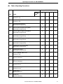
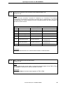
Customer Notification QB-V850ESSX2 In-Circuit-Emulator Operating Precautions Target Device V850ES/SG1 V850ES/SG2 V850ES/SJ2 V850ES/SG2H V850ES/SJ2H V850ES/SG3 V850ES/SJ3 V850ES/JG2 V850ES/JJ2 Document No. Date Published U18703EE1V0IF00 March 2007 NEC Electronics (Europe) GmbH DISCLAIMER The related documents in this customer notification may include preliminary versions. However, preliminary versions may not have been marked as such. The information in this customer notification is current as of its date of publication. The information is subject to change without notice. For actual design-in, refer to the latest publications of NEC’s data sheets or data books, etc., for the most up-to-date specifications of NEC PRODUCT(S). Not all PRODUCT(S) and/or types are available in every country. Please check with an NEC sales representative for availability and additional information. No part of this customer notification may be copied or reproduced in any form or by any means without prior written consent of NEC. NEC assumes no responsibility for any errors that may appear in this customer notification. NEC does not assume any liability for infringement of patents, copyrights or other intellectual property rights of third parties by or arising from the use of NEC PRODUCT(S) listed in this customer notification or any other liability arising from the use of such PRODUCT(S). No license, express, implied or otherwise, is granted under any patents, copyrights or other intellectual property rights of NEC or others. Descriptions of circuits, software and other related information in this customer notification are provided for illustrative purposes of PRODUCT(S) operation and/or application examples only. The incorporation of these circuits, software and information in the design of customer’s equipment shall be done under the full responsibility of customer. NEC assumes no responsibility for any losses incurred by customers or third parties arising from the use of these circuits, software and information. While wherever feasible, NEC endeavors to enhance the quality, reliability and safe operation of PRODUCT(S) the customer agree and acknowledge that the possibility of defects and/or erroneous thereof cannot be eliminated entirely. To minimize risks of damage to property or injury (including death) to persons arising from defects and/or errors in PRODUCT(S) the customer must incorporate sufficient safety measures in their design, such as redundancy, fire-containment and anti-failure features. The customer agrees to indemnify NEC against and hold NEC harmless from any and all consequences of any and all claims, suits, actions or demands asserted against NEC made by a third party for damages caused by one or more of the items listed in the enclosed table of content of this customer notification for PRODUCT(S) supplied after the date of publication. Applicable Law: The law of the Federal Republic of Germany applies to all information provided by NEC to the Customer under this Operating Precaution document without the possibility of recourse to the Conflicts Law or the law of 5th July 1989 relating to the UN Convention on Contracts for the International Sale of Goods (the Vienna CISG agreement). Düsseldorf is the court of jurisdiction for all legal disputes arising directly or indirectly from this information. NEC is also entitled to make a claim against the Customer at his general court of jurisdiction. If the supplied goods/information are subject to German, European and/or North American export controls, the Customer shall comply with the relevant export control regulations in the event that the goods are exported and/or re-exported. If deliveries are exported without payment of duty at the request of the Customer, the Customer accepts liability for any subsequent customs administration claims with respect to NEC. Notes: 1. “NEC” as used in this statement means NEC Corporation and also includes its direct or indirect owned or controlled subsidiaries. 2. “PRODUCT(S)” means ‘NEC semiconductor products’ (NEC semiconductor products means any semiconductor product developed or manufactured by or for NEC) and/or ‘TOOLS’ (TOOLS means ‘hardware and/or software development tools’ for NEC semiconductor products’ developed, manufactured and supplied by ‘NEC’ and/or ‘hardware and/or software development tools’ supplied by NEC but developed and/or manufactured by independent 3rd Party vendors worldwide as their own product or on contract from NEC) 2 Customer Notification U18703EE1V0IF00 Operating Precautions for QB-V850ESSX2TM (A) Product Version. . . . . . . . . . . . . . . . . . . . . . . . . . . . . . . . . . . . . . . . . . . . . . . . . 2 (B) Table of Operating Precautions . . . . . . . . . . . . . . . . . . . . . . . . . . . . . . . . . . . . 3 (C) Description of Operating Precautions. . . . . . . . . . . . . . . . . . . . . . . . . . . . . . . 6 (D) Valid Specification . . . . . . . . . . . . . . . . . . . . . . . . . . . . . . . . . . . . . . . . . . . . . 35 (E) Revision History . . . . . . . . . . . . . . . . . . . . . . . . . . . . . . . . . . . . . . . . . . . . . . . 36 Customer Notification U18703EE1V0IF00 1 Operating Precautions for QB-V850ESSX2 (A) Product Version 1. Product Code: QB-V850ESSX2 Control CodeNote 1 E Usable Exec VersionNote 2 EX850G32.dll, Version 1.77 Usable Device File Package VersionNote 2 V850ES/SG1: IE-703252, Version V1.00 IE-703253, Version V1.00 V850ES/SG2: IE-703283, Version V2.11 V850ES/SJ2: IE-703288, Version E2.11 V850ES/SG2H: IE-703283H, Version V1.00 V850ES/SJ2H: IE-703288H, Version V1.00 V850ES/SG3, V850ES/SJ3: IE-703368, Version V1.01 V850ES/JG2, V850ESJJ2: IE-703724, Version V1.00 Notes: 1. The Control Code is indicated by the letter appearing at the 2nd position from the left in the serial number of the product. 2. The usable exec and device file packages versions listed were checked in time of release of this document. Please check the NEC website regularly for newer versions. Customer Notification U18703EE1V0IF00 2 Operating Precautions for QB-V850ESSX2 (B) Table of Operating Precautions QB-V850ESSX2 No. ControlCodeNote Outline A C D E 1 Watchdog timer during break (Direction of use) ✗ ✗ ✗ ✗ 2 Timer M during break (Direction of use) ✗ ✗ ✗ ✗ 3 Timer M compare interrupt (Specification change notice) ✗ ✗ ✗ ✗ 4 Access of UAnRX register during break (Specification change notice) ✗ ✗ ✗ ✗ 5 Access of CBnRX register during break (Specification change notice) ✗ ✗ ✗ ✗ 6 Access of C0RGPT register during break (Specification change notice) ✗ ✗ ✗ ✗ 7 Access of C0TGPT register during break (Specification change notice) ✗ ✗ ✗ ✗ 8 Access of C0GNCTRL register during break (Specification change notice) ✗ ✗ ✗ ✗ 9 Guarded area access break delay (Specification change notice) ✗ ✗ ✗ ✗ 10 Hardware break points (Specification change notice) ✗ ✗ ✗ ✗ 11 Access to DBPSW, DBPC, ECR (Direction of use) ✗ ✗ ✗ ✗ 12 DMA transfer forcible termination (Technical Limitation) ✗ ✗ ✓ ✓ 13 Program execution and DMA transfer in internal RAM (Technical Limitation) ✗ ✗ ✓ ✓ 14 Power saving (NOP insertion) (Direction for use) ✗ ✗ ✗ ✗ 15 Pin control with target power off (Direction for use) ✗ ✗ ✗ ✗ 16 Reset by WDT (Technical Limitation) ✗ ✗ ✓ ✓ 17 Reset by LVI (Technical Limitation) ✗ ✗ ✓ ✓ Customer Notification U18703EE1V0IF00 3 Operating Precautions for QB-V850ESSX2 QB-V850ESSX2 A C D E Download to IROM (Specification change notice) ✗ ✗ ✗ ✗ 19 CLKOUT signal in Standby mode (Direction for use) ✗ ✓ ✓ ✓ 20 Standby mode when interrupt is pending (Specification change notice) ✗ ✗ ✗ ✗ 21 SLD instruction precaution (Specification change notice) ✗ ✗ ✗ ✗ 22 IROM access at 20 MHz operation (Technical limitation) ✗ ✓ ✓ ✓ 23 Break during program execution in internal RAM (1) (Specification change notice) ✗ ✗ ✗ ✗ 24 Reset input during break (Technical limitation) ✗ ✗ ✓ ✓ 25 Emulation of ROM Correction (Direction of use) ✗ ✗ ✗ ✗ 26 Emulation of Flash self programming (Direction of use) ✗ ✗ ✗ ✗ 27 Non map break (Direction of use) ✗ ✗ ✗ ✗ 28 DBTRAP instruction (Direction of use) ✗ ✗ ✗ ✗ 29 PSC register access (Direction of use) ✗ ✗ ✗ ✗ 30 Trace display order (Direction of use) ✗ ✗ ✗ ✗ 31 Extension probe (Direction of use) ✗ ✗ ✗ ✗ 32 Simultaneous execution of two instructions when hardware break is set (Direction of use) ✗ ✗ ✗ ✗ 33 TMPn / TMQn external event counter function (Direction of use) ✗ ✗ ✗ ✗ 34 TMPn / TMQn capture operation (Direction of use) ✗ ✗ ✗ ✗ 35 Internal ROM misfetch (Technical limitation) ✗ ✓ ✓ ✓ No. Outline 18 ControlCodeNote Customer Notification U18703EE1V0IF00 4 Operating Precautions for QB-V850ESSX2 QB-V850ESSX2 ✓ ✗ ControlCodeNote A C D E Data loss when external RAM is connected (Direction of use) ✗ ✗ ✗ ✗ 37 New version of Evachip (Direction of use) ✓ ✓ ✗ ✗ 38 aFCAN: Rx limitation (Technical limitation) ✗ ✗ ✗ ✓ 39 Behaviour of STOP mode release when RESET pin is masked (Specification change notice) ✗ ✗ ✗ ✗ 40 ADC: Conversion function during break (Specification change notice) ✗ ✗ ✗ ✗ 41 Clock supply specification (Technical limitation) ✗ ✗ ✗ ✓ 42 Support of optional functions (Direction of use) ✓ ✓ ✓ ✗ 43 Break during program execution in internal RAM (2) (Specification change notice) ✗ ✗ ✗ ✗ 44 Address is not retained during external bus access (Specification change notice) ✗ ✗ ✗ ✗ No. Outline 36 Not applicable Applicable Note: The Control Code is indicated by the letter appearing at the 2nd position from the left in the serial number of the product. Customer Notification U18703EE1V0IF00 5 Operating Precautions for QB-V850ESSX2 (C) Description of Operating Precautions No. 1 Watchdog timer during break (Direction of use) Details When both of the following conditions (a) and (b) are fulfilled simultanously and a break occurs, the watchdog timer does not stop and will cause a reset or non maskable interrupt. If a reset occurs, the debugger hangs up. Conditions that need to be fulfilled so that the above behaviour occurs: (a) The main clock or subclock is selected as the clock source of the watchdog timer and (b) The ring oscillator is stopped (RSTOP flag = 1). Workaround As a workaround to prevent the above behaviour do not stop the ring oscillator clock. No. 2 Timer M during break (Direction of use) Details When a break occurs while the following conditions (a) and (b) are both fulfilled, timer M does not stop even if the peripheral break function has been set to ’break’. (a) INTWT, Ring oscillator clock (fR/8) or subclock is selected as the clock source for timer M. (b) The main clock is stopped by setting the MCK flag. (Note: The peripheral break function is not supported by the debugger ID850 V2.51.) Workaround Implement one of the below workarounds to stop timer M during a break using the peripheral break function: (a) Use the main clock (fXX, fXX/2, fXX/4, fXX/64, fXX/512) as the source clock for timer M. (b) Do not stop the main clock oscillation. Customer Notification U18703EE1V0IF00 6 Operating Precautions for QB-V850ESSX2 No. 3 Timer M compare interrupt (Specification change notice) Details An unexpected interrupt occurs after activation of timer M when the compare register TM0CMP0 contains the value 0xFFFF. TMM starts to operate TM0CE TMM 16bit counter FFFFH 0000H 0001H 0002H TM0CMP0 FFFEH FFFFH 0000H FFFFH INTTMEQ0 Interrupt Workaround Do not set TM0CMP0 to 0xFFFF. Customer Notification U18703EE1V0IF00 7 Operating Precautions for QB-V850ESSX2 No. 4 Access of UAnRX register during break (Specification change notice) Details An overrun error occurs under the following conditions (a) to (c): (a) If a break occurs after reading the UART receive buffer register (UAnRX) and the UAnRX register is displayed in the I/O register window of the debugger, an overrun error occurs when UART reception is performed for the next time. (b) If a software break occurs immediately after reading the UART receive buffer register (UAnRX), an overrun error occurs when UART reception is performed the next time regardless of whether or not the UAnRX register is displayed in the I/O register window. (c) If a DMA transfer from the UART receive buffer register (UAnRX) is performed during a breakNOTE, an overrun error occurs when UART reception is performed the next time. Note: Including breaks by the RAM monitor function or DMM function. However the realtime RAM monitor function does not cause this behaviour since it does not set breaks. Remark: An overrun error also occurs when the UART receives data multiple times during a break (This complies with the specification of the emulator). Workaround (a) Do not display the UAnRX register in the I/O register window. (b) Set a hardware break when setting a break immediately after reading the UAnRX register (c) There is no workaround. No. 5 Access of CBnRX register during break (Specification change notice) Details When the CSIBn receive data register (CBnRX) is read, it usually starts the next reception operation. Under the following conditions (a) and (b), however, the next reception operation is not started even if CBnRX is read. (a) If a software break occurs immediately after reading the CSIBn receive register (CBnRX). (b) If a DMA transfer from the CSIBn receive data register (CBnRX) is performed during a breakNOTE. As a result the communication stops or the DMA controller stops. Note: Including breaks by the RAM monitor function or DMM function. However the realtime RAM monitor function does not cause this behaviour since it does not set breaks. Workaround (a) Set a hardware break when setting a break immediately after reading the CBnRX register. (b) There is no workaround. Customer Notification U18703EE1V0IF00 8 Operating Precautions for QB-V850ESSX2 No. 6 Access of C0RGPT register during break (Specification change notice) Details Under the following conditions (a) and (b), the read pointer (RGPT) that should be incremented is not incremented and the same data as previously read is read again. (a) If a software break occurs immediately after reading the CAN0 module receive history list register (C0RGPT) (b) If a DMA transfer from the CAN0 module receive history list register (C0RGPT) is performed during a breakNOTE. Note: Including breaks by the RAM monitor function or DMM function. However the realtime RAM monitor function does not cause this behaviour since it does not set breaks. Workaround (a) Set a hardware break when setting a break immediately after reading the C0RGPT register. (b) There is no workaround. No. 7 Access of C0TGPT register during break (Specification change notice) Details Under the following conditions (a) and (b), the read pointer (TGPT) that should be incremented is not incremented and the same data as previously transmitted is transmitted again. (a) If a software break occurs immediately after reading the CAN0 module transmit history list register (C0TGPT). (b) If a DMA transfer from the CAN0 module transmit history list register (C0TGPT) is performed during a breakNOTE. Note: Including breaks by the RAM monitor function or DMM function. However the realtime RAM monitor function does not cause this behaviour since it does not set breaks. Workaround (a) Set a hardware break when setting a break immediately after reading the C0TGPT register. (b) There is no workaround. Customer Notification U18703EE1V0IF00 9 Operating Precautions for QB-V850ESSX2 No. 8 Access of C0GNCTRL register during a break (Specification change notice) Details When a register access is performed in the following sequence, an unexpected forcible shutdown may occur after the sequence is complete. Sequence : (1) The EFSD bit of the CAN0 module control register (C0GMCTRL) is set. (2) The I/O registerNOTE is accessed. (3) The GOM bit of the CAN0 mode control register (C0GMCTRL) is cleared. Note: I/O register access except for clearing the GOM bit of the C0GMCTRL register The conditions under which a forcible shutdown takes place are shown below: (a) If a break occurs immediately after the I/O register access in (2) occurs. (b) If a break by the RAM monitor function or the DMM function occurs immediately after the I/O register access in (2) occurs. (c) Stepwise execution is performed for the I/O register access in (2). Workaround Be sure to set the EFSD bit and clear the GOM bit successively when executing a forcible shutdown. Do not perform a register access in the above sequence when not performing a forcible shutdown. No. 9 Guarded area access break delay (Specification change notice) Details When a guarded area is entered by a jump instruction, the guard access break is not generated for around the first 5 instructions. A delay occurs. Workaround There is no workaround. Customer Notification U18703EE1V0IF00 10 Operating Precautions for QB-V850ESSX2 No. 10 Hardware break points (Specification change notice) Details Assembly level: When break points are set to two consecutive instructions and a break is generated by the first instruction, the second break may not be generated after the subsequent start command. 0x80049c 0x80049e 0x8004a0 mov r9, r10 add r7, r10 addi 1, r10, r17 <--- Break point setting <--- Break point setting Source level: When break points are set to two consecutive executable instructions (each of which consists of a single instruction) and a break is generated by the first statement, then the second statement may not generate a break after the subsequent start command. 10 11 a = b; a += c; (mov r9, r10) (add r7, r10) <--- Break point setting <--- Break point setting Workaround ID850: Follow the software break point setting instructions in the debugger documentation. GHS Multi: Use EX85032.DLL Version 5.40 or later. There is no workaround for the hardware break. No. 11 Access to DBPSW, DBPC, ECR (Direction of use) Details DBPSW, DBPC and ECR cannot be accessed in break mode. If written, the value is discarded, if read 0 is always read. Workaround There is no workaround. Customer Notification U18703EE1V0IF00 11 Operating Precautions for QB-V850ESSX2 No. 12 DMA transfer forcible termination (Technical limitation) Details When terminating a DMA transfer by setting the corresponding INITn bit of the DCHCn register, the transfer may not be terminated, but just suspended, even though the INITn bit is set (1). As a result, when the DMA transfer of a channel that should have been terminated is resumed, the DMA transfer will terminate after an unexpected number of transfers are completed and a DMA transfer completion interrupt may occur. In addition, a DMA transfer of a channel n for which the INITn bit is set after forcible termination may be performed once again with the initialized value (n= 0 to 3). The critical situation occurs if a DMA transfer is executed immediately after a forcible termination is set (by setting the INITn bit), refer to figure below. The critical timing does not depend on the number of transfer channels, transfer type, transfer target, transfer mode, or trigger, and can occur with any combination of the above elements that can be set under the specifications. In addition, another channel may affect the occurrence of this critical timing. Operation example: Both DMA channels, ch 0 and ch 1, are in single transfer mode, and ch 1 DMA transfer count is 3 (DBC1 register value = 02H). Ch 0 DMA transfer (DMAAK signal) Ch 1 DMA transfer (DMAAK signal) Critical timing when Ch 0 DMA transfer is performed immediately after setting the INIT1 bit to 1 Ch 1 forcible termination (INIT1 bit) Ch 1 DMA transfer enable setting (DMA transfer is resumed by a DMA trigger after DMA transfer is enabled) Ch 1 DMA transfer enable (E11 bit) DBC1 register value (Critical timing: Suspended) DBC1 register value (Normal: Terminated) 02H 01H 00H 02H Normally, DBC1 register value must be initialized when the INIT1 bit is set. 02H 01H 02H 01H 00H 02H INTDMA1 Normal operation Interrupt occurrence caused by critical timing Normal interrupt occurrence The following registers are buffer register with a 2-stage FIFO configuration of master and slave: • DMA source address register (DSAnH, DSAnL) • DMA destination address register (DDAnH, DDAnL) • DMA transfer count register (DBCn) If these registers are overwritten during a DMA transfer, or in the DMA suspended status, the value is written to the master register, and reflected in the slave register when the DMA transfer of the overwritten channel is terminated. The “initialization” in the figure above means that the contents of the master register are reflected in the slave register. Customer Notification U18703EE1V0IF00 12 Operating Precautions for QB-V850ESSX2 No. 12 DMA transfer forcible termination (Technical limitation) (cont.) Workaround The critical situation can be avoided by implementing any of the following procedures. <1> Stop all transfers from DMA channels temporarily. The following measure is effective if the program does not assume that the TCn bit of the DCHCn register is 1 except for the following workaround processing. (Since the TCn bit of the DCHCn register is cleared (0) when it is read, execution of the following procedure b) under <5> clears this bit.) Procedure to avoid the critical timing: <1> Disable interrupts (DI state) <2> Read the DMA restart register (DRST) and transfer the ENn bit of each channel to a general purpose register (value A). <3> Write 00H to the DMA restart register (DRST) twiceNote. By executing twiceNote, the DMA transfer is definitely stopped before proceeding to <4>. <4> Set (1) the INITn bit of the DCHCn register of the channel that should be terminated forcibly. <5> Perform the following operations for value A read in (2) to obtain value B. a) Clear (0) the bit of the channel that is not terminated forcibly. b) If the TCn and ENn bits of the channel that is not terminated forcibly are 1, clear (0) the bit of the channel. <6> Write value B in <5> to the DRST register. <7> Enable interrupts (EI state) Note: Execute three times if the transfer target (transfer source or transfer destination) is the internal RAM. Remarks: 1. Be sure to execute <5> to prevent the ENn bit from being set illegally for channels that are terminated normally during the period of <2> and <3> 2. n = 0 to 3 <2> Repeat setting the INITn bit until the forcible DMA transfer termination is correctly performed (n = 0 to 3) Procedure to avoid the critical timing: <1> Copy the initial transfer count of the channel that should be terminated forcibly to a general-purpose register. <2> Set (1) the INITn bit of the DCHCn register of the channel that should be terminated forcibly. <3> Read the value of the DMA transfer count register (DBCn) of the channel that should be terminated forcibly and compare the value with the one copied in <1>. If the value do not match, repeat <2> and <3>. Remarks: 1. When the DBCn register is read in procedure <3>, the remaining transfer count will be read if the DMA is stopped due to this bug. If the forcible DMA termination is performed correctly, the initial transfer count will be read. 2. Note that it may take some time for forcible termination to take effect if this workaround is implemented in an application in which DMA transfer other than for channels subject to forcible termination are frequently performed. Customer Notification U18703EE1V0IF00 13 Operating Precautions for QB-V850ESSX2 No. 13 Program execution and DMA transfer in internal RAM (Technical limitation) Details When a DMA transfer for the internal RAM and a bit manipulation instruction (SET1, CLR1, or NOT1) allocated in the internal RAM or a data access instruction for a misaligned address are executed simultaneously, the CPU may deadlock due to conflict between the internal bus operations. At this time, only a reset can be acknowledged, an NMI or an maskable interrupt cannot be acknowledged any more. Unaffected cases The critical situation does not occur if no instruction is executed in the internal RAM, or no DMA transfer is performed on the internal RAM. Workaround Implement any of the following workarounds. • Do not perform a DMA transfer for the internal RAM when an instruction allocated in the internal RAM is being executed. • Do not execute an instruction allocated in the internal RAM when a DMA transfer for the internal RAM is being performed. Customer Notification U18703EE1V0IF00 14 Operating Precautions for QB-V850ESSX2 No. 14 Power saving (NOP insertion) (Direction for use) Details To save power, be sure to insert five NOP instructions after executing the HALT instruction and an instruction that sets the STB (or STP) bit of PSC register. a) STB (or STP) bit (PSC register) setting instruction mov movea st.b st.b nop nop nop nop nop b) 0x2, r11 base_address, r0, r20 r11, PRCMD[r20] r11, PSC[r20] ; base_address = FFFF0000H ; PRCMD = 01FCH ; PSC = 01FEH ; insert five nop’s HALT instruction halt nop nop nop nop nop ; insert five nop’s Customer Notification U18703EE1V0IF00 15 Operating Precautions for QB-V850ESSX2 No. 15 Pin control with target power OFF (Direction for use) Details When power to the emulator is ON and that to the target is OFF, leakage current may flow from the emulator to the target. When the target is connected, the emulator always senses the target supply voltage by using a target supply voltage detector circuit, and the emulator is automatically reset when the target power is turned ON or OFF. In this reset status, the external bus signal go inter a high-impedance state. Some external bus signals, however, drive a high level, and a current may leak into Vdd of the target via the pull-up resistor of the target. The target supply voltage detector circuit of the emulator detects this VDD, and the emulator assumes that power is applied to the target. Consequently, reset is cleared and the external bus signals are driven. As a result, a leakage current flows. Target VDD ICE Target VDD ON/OFF Detect EVACHIP IETGTOFF Device Power Loop No. 16 Reset by WDT (Technical limitation) Details The emulator may hang up when a reset is generated by the WDT. Therefore do not start the WDT at the beginning. Workaround There is no workaround. Customer Notification U18703EE1V0IF00 16 Operating Precautions for QB-V850ESSX2 No. 17 Reset by LVI (Technical limitation) Details The emulator may hang up when a reset is generated by the LVI. Therefore take care not to activate reset generation by LVI. Workaround There is no workaround. No. 18 Download to IROM (Specification change notice) Details The emulator may hang up when an active signal is connected to the WAIT or HLDRQ pin of the external bus interface during program download or a software breakpoint is set to the internal ROM area. Workaround If WAIT or HLDRQ are not used, mask these signals using the mask function of the debugger. If WAIT or HLDRQ are used, do not make these pins active while data is beeing downloaded to the internal ROM area or a software break is set to the internal ROM area. The above behaviour can be avoided by using the following software tool components: ID850: Use version 2.81 of the ID850 or later. Green Hills Multi: Use the EXEC V1.57 or later. Customer Notification U18703EE1V0IF00 17 Operating Precautions for QB-V850ESSX2 No. 19 CLKOUT signal in standby mode (Direction for use) Details In STOP or IDLE mode the state of the CLKOUT pin differs from the device specification. Instead of low level, the CLKOUT signal is continuously output on the CLKOUT pin. This behaviour does not apply to the HALT mode. Workaround If output of the CLKOUT signal in standby modes causes problems make sure that a low level is output at the CLKOUT pin before entering the standby mode using the following procedure: - Clear bit 1 of the PMCCM register to 0 (switch to I/O) - Clear bit 1 of the PMCM register to 0 (select output mode) - Clear bit 1 of the PCM register to 0 (output low-level) If the above procedure is implemented, set bit 1 of PMCCM register to 1 immediately after release of the standby mode to output CLKOUT. The above behaviour can be avoided in Control Code Version ’D’ of the Emulator if the following software tool components are used: ID850: Use version 2.81 of the ID850 or later. Green Hills Multi: Use the EXEC V1.57 or later. No. 20 Standby mode when interrupt is pending (Specification change notice) Details When an interrupt is pending it is not possible to enter standby mode. Workaround There is no workaround. Customer Notification U18703EE1V0IF00 18 Operating Precautions for QB-V850ESSX2 No. 21 SLD instruction precaution (Specification change notice) Details If a conflict occurs between the decode operation of the instruction (<2> in the examples mentioned below) immediately before the sld instruction (<3> in the examples) following a special instruction (<1> in the examples) and an interrupt request before execution of the special instruction is complete, the execution result of the special instruction may not be stored in a register as expected. This situation may only occur when the same register is used as the destination register of the special instruction and the sld instruction, and when the register value is referenced by the instruction followed by the sld instruction. Conditions under which the conflict occurs: The situation may occur when all the following conditions (1) to (3) are satisfied. (1) Either condition (I) or (II) is satisfied Condition (I): The same register is used as the destination register of a special instruction (see below) and the subsequent sld instruction and as the source register (reg1) of an instruction shown below followed by the sld instruction (See Example 1). mov reg1,reg2 satadd reg1,reg2 tst reg1,reg2 cmp reg1,reg2 not reg1,reg2 or reg1,reg2 subr reg1,reg2 mulh reg1,reg2 satsubr reg1,reg2 xor reg1,reg2 sub reg1,reg2 satsub reg1,reg2 and reg1,reg2 add reg1,reg2 Condition (II): The same register is used as the destination register of a special instruction (see below) and the subsequent sld instruction and as the source register (reg2) of an instruction shown below followed by the sld instruction (See Examples 2 and 3). not reg1,reg2 satadd imm5,reg2 tst reg1,reg2 add imm5,reg2 sar imm5,reg2 satsubr reg1,reg2 or reg1,reg2 subr reg1,reg2 cmp reg1,reg2 shl imm5,reg2 satsub reg1,reg2 xor reg1,reg2 sub reg1,reg2 cmp imm5,reg2 satadd reg1,reg2 and reg1,reg2 add reg1,reg2 shr imm5,reg2 Special instruction: • ld instruction: ld.b, ld.h, ld.w, ld.bu, ld.hu • sld instruction: sld.b, sld.h, sld.w, sld.bu, sld.hu • Multiply instruction: mul, mulh, mulhi, mulu (2) When the execution result of the special instruction (see above) has not been stored in the destination register before execution of the instruction (instruction of condition (I) or (II)) immediately before the sld instruction starts in the CPU pipeline. Customer Notification U18703EE1V0IF00 19 Operating Precautions for QB-V850ESSX2 No. 21 SLD instruction precaution (Specification change notice) (cont.) (3) When the decode operation of the instruction (instruction of condition (I) or (II)) immediately before the sld instruction and interrupt request servicing conflict. Examples of instruction sequences that may cause the conflict: Example 1: <1> ld.w [r11], r10 This situation occurs when the decode operation of the mov instruction (<2>) immediately before the sld instruction (<3>) and interrupt request servicing conflict before the execution of the special instruction ld (<1>) is complete. .. . <2> mov r10, r28 <3> sld.w 0x28, r10 Example 2: <1> ld.w [r11], r10 .. . <2> cmp imm5, r10 <3> sld.w 0x28, r10 <4> bz label This situation occurs when the decode operation of cmp (<2>) immediately before the sld instruction (<3>) and interrupt request servicing conflict before execution of the special instruction ld (<1>) is complete. As a result, the compare result of the cmp instruction becomes undefined, which may cause an unexpected operation of the branch instruction bz (<4>). Example 3: <1> ld.w [r11], r10 .. . <2> add imm5, r10 <3> sld.w 0x28, r10 <4> setf c, r16 This situation occurs when the decode operation of the add instruction (<2>) immediately before the sld instruction (<3>) and interrupt request servicing conflict before execution of the special instruction ld (<1>) is complete. As a result, the result of the add instruction and the depending status flags become undefined, which may cause an unexpected operation of the setf instruction (<4>). Workaround (1) Do not use the sld instruction (e. g. by avoiding code optimization that makes use of sld). (2) If a code sequence as described above is used (a sld instruction following an instruction that can be executed in parallel), insert a nop instruction before the sld instruction. (3) If a code sequence as described above is used (a sld instruction following an instruction that can be executed in parallel), exchange the order of the previous two instructions as long as the program algorithm is not disturbed: Customer Notification U18703EE1V0IF00 20 Operating Precautions for QB-V850ESSX2 No. 21 SLD instruction precaution (Specification change notice) (cont.) Example: 1. (before implementing workaround) ld.w [r11], r10 ... add r11, r12 mov r10, r28 sld.w 0x28, r10 2. (after implementing workaround) ld.w [r11], r10 ... mov r10, r28 add r11, r12 sld.w 0x28, r10 (4) When assembler code is used: Avoid the crictical code sequences as described above. No. 22 IROM access at 20 MHz operation (Technical limitation) Details Code/data fetched from internal ROM (IROM) of the emulator may be read incorrectly when operated in non-interleaved mode (e. g. at 20 MHz operation speed). The data is read correctly when operating in interleaved mode (e. g. at 32 MHz operation speed). Emulator version control code ’C’ can only be used at operation speeds up to 20 MHz. Workaround This issue does not apply to control code ’D’ or later. Customer Notification U18703EE1V0IF00 21 Operating Precautions for QB-V850ESSX2 No. 23 Break during program execution in internal RAM (1) (Specification change notice) Details An unexpected break may occur when a peripheral I/O register is accessed during program execution in internal RAM. Workaround Cancel the fail-save break setting for the internal RAM in the debugger. a) When using the ID850 debugger: Select Configuration/Fail-save Break/Detail and clear the check box ’Non Map’ for ’Internal RAM’. b) When using Green Hills Multi: Cancel the fail-save break for ’ramgrd’ and ’ramgrdv’ unsing the Target command ’flsf’. No. 24 Reset input during break (Technical limitation) Details The QB-V850ESSX2 may hang up if a break occurs when the RESET pin is active (low level). Workaround Mask the RESET pin using the pin mask function of the debugger. No. 25 Emulation of ROM Correction (Direction of use) Details The ROM correction function cannot be emulated. Workaround Evalutate the ROM correction function using the target device. Customer Notification U18703EE1V0IF00 22 Operating Precautions for QB-V850ESSX2 No. 26 Emulation of Flash self programming (Direction of use) Details The flash selfprogramming function cannot be emulated. Workaround Evalutate the flash self programming function using the on-chip debug emulator or the target device. No. 27 Non map break (Direction of use) Details If a program fetch is performed on an unused memory area in the emulator normally a non map break occurs. However the non map break is not generated in the top 16 bytes of unused areas. Workaround There is no workaround. No. 28 DBTRAP instruction (Direction of use) Details The DBTRAP function cannot be used. Workaround There is no workaround. Customer Notification U18703EE1V0IF00 23 Operating Precautions for QB-V850ESSX2 No. 29 PSC register access (Direction of use) Details The debugger hangs up if a software break is set at the NOP instruction immediately after the PSC register is accessed. Workaround Example: MOV 0x2, R1 ST.B R1, PRCMD ST.B R1, PSC NOP <- The debugger hangs up if a software break is set here NOP <- Setting a software break hereafter causes no problem Use a hardware break to set a break immediately after the PSC register is accessed. No. 30 Trace display order (Direction of use) Details When the trace mode is used to display the access history the displayed order may be reversed in the following cases: a) When a write instruction follows a read instruction. b) When a bit manipulation instruction that performs a read/modify/write operation (SET, NOT, CLR) is performed In both cases the trace result is displayed in the following order: 1st: write, 2nd: read. Workaround There is no workaround. No. 31 Extension probe (Direction of use) Details If the extension probe cable is used the access to the external memory bus interface is limited. Workaround Increase the number of data wait cycles by one. The number of data wait cycles is set in the DWC (data wait control) register. Customer Notification U18703EE1V0IF00 24 Operating Precautions for QB-V850ESSX2 No. 32 Simultaneous execution of two instructions when hardware break is set (Direction of use) Details Suppose that two instructions ’instruction A’ followed by an ’instruction B’ are executed simultaneously. The execution result of these instructions when a hardware break is set is shown in the table below. As a result the break may occur at a different location from the set address, or the break may even not occur. Break Timing No. Instruction A Instruction B Execution Result 1 Break before execution No break setting Break before execution of A 2 Break after execution No break setting Break after execution of B 3 No break setting Break before execution Break before execution of A 4 No break setting Break after execution Break after execution of B 5 Break before execution Break before execution Break before execution of A 6 Break before execution Break after execution Break before execution of A and after execution of B 7 Break after execution Break before execution Break before execution of A and after execution of B 8 Break after execution Break after execution Break after execution of B Workaround To avoid the above behaviour set a software break instead of a hardware break. No. 33 TMPn / TMQn external event counter function (Direction of use) Details When the external event counter mode is used and the compare register of timer TMP or TMQ is set to 0x0000 an interrupt occurs after the overflow of the timer. Workaround Avoid setting 0x0000 to the timer compare registers of TMP or TMQ. Customer Notification U18703EE1V0IF00 25 Operating Precautions for QB-V850ESSX2 No. 34 TMPn / TMQn capture operation (Direction of use) Details When the pulse width measurement mode or the free-running mode are used the initial value of the capture register is 0xFFFF when the count clock of the TMPn / TMQn is lower than the sampling clock of the capture trigger input after the timer is enabled (TPnCE = 1, TQnCE = 1). Workaround There is no workaround. No. 35 Internal ROM misfetch (Technical limitation) Details A misfetch may occur during program execution in the internal ROM (an unexpected instruction is executed). Workaround There is no workaround. This behaviour has been fixed in versions newer than control code ’A’. No. 36 Data loss when external RAM is connected (Direction of use) Details A write cycle to the external bus is generated when downloading data to the internal ROM or a software break is set to the internal ROM. Therefore, if RAM is connected to the target system, data in that RAM may be lost. Workaround In case of downloading data into internal ROM there is no workaround. If the data in internal RAM is initialized by program execution after download (all values in internal RAM are overwritten) there is no problem since all data is overwritten by the desired values. In case of a software break in internal ROM: Do not use a software breakpoint in internal ROM. Use a hardware breakpoint instead. The above behaviour can be avoided by using the following software components: - ID850: Use the version 2.81 or later of the ID850 debugger. - Green Hills Multi: Use the version V1.57 or later of the exec.dll. Customer Notification U18703EE1V0IF00 26 Operating Precautions for QB-V850ESSX2 No. 37 New version of Evachip (Direction of use) Details: A new evachip version is used from the tool version of control code ’D’ onwards: uPD703195A. For use with the Greenhills Multi debugger use the following or newer versions of these software components: EX850G32.dll: use version V1.57 or later 850ESERV.exe: use version 2.224 or later Customer Notification U18703EE1V0IF00 27 Operating Precautions for QB-V850ESSX2 No. 38 aFCAN: Rx limitation (Technical limitation) Details RX Limitation The aFCAN macro may store an incoming message although this message was interrupted by a bus error frame. Thus, the incomplete reception causes that a message buffer is updated with old or incorrect data or that the message is even stored at an incorrect location. This unexpected behaviour affords that the bus error occurs in a certain relation to the currently present message on the bus. The critical time window starts at the sample point of the LSB of the DLC-field and lasts for the duration of an internal process in the aFCAN macro (RX-search). This time window usually lasts for a few bit times only. The actual length depends on the clock supply for the AFCAN, the CPU accesses during this period, the baud rate and the number of message buffers of the particular AFCAN macro. In this time window the RX-search evaluates the received identifier of the current message. When the bus error is detected within this window and when the RX-search has just scanned buffer #n for reception and found it is matching, the message will unexpectedly be treated as a received message. As the time window is limited as described above, only a stuff bit error occurring right in this window can cause this behaviour. There are two types of unexpected behavior for the RX limitation depending on the presence of pending transmission request (TRQ) for any other message buffer. 1. Behaviour at pending TRQ (TRQi = 1) When the host processor has already submitted a transmit request (TRQ) for at least one buffer, the unexpected reception of the message will take place into the message buffer found by internal RX-search. This is the correct location to store the message i.e. the acceptance filter criteria are correctly fulfilled. However the data part will be updated with the contents of the shift register of the CAN protocol core. As this register is immediately stopped at detection of the bus error, the data provided to the message buffer can not be interpreted by the host processor. TRQi=1 Stuff Error CAN bus Rx Frame Error Frame IM RX/TX Frame INTERR zoomed Internal action INTREC Rx Search Scanning Msg#n Figure 1: Behavior at pending TRQ As during a regular reception, the RX-interrupt (if enabled) is generated and the application processes the message object. Customer Notification U18703EE1V0IF00 28 Operating Precautions for QB-V850ESSX2 No. 38 aFCAN: Rx limitation (Technical limitation) (cont.) 2. Behavior without pending TRQ (TRQi = 0) In case the host processor has not submitted a transmit request (TRQ) for any buffer before the detection of the bus error but submits TRQ = 1 after that point in time (see figure below) before the re-transmission of the message interrupted by the stuff bit error started, the unexpected reception of the message will take place. TRQi=1 Stuff Error CAN bus Error Frame Rx Frame INTERR IM RX/TX Frame INTREC zoomed Internal action Rx Search Scanning Msg#n Figure 2: Behavior without pending TRQ The unexpected storage of the message is issued in the particular message buffer that matches the acceptance filter criteria at the time where the bus error is detected (as described in 1.) or the message buffer #0 is overwritten independently of its configuration. Impact on application In typical applications the RX-limitation will lead to transiently incorrect data. In the vast majority of cases the message interrupted by a bus error is repeated by the transmitter right away. Then the application receives correct data shortly after the unexpected reception. In scenarios where the message buffer #0 is overwritten, the impact for the application depends on the usage of that buffer. If it is configured as a receive buffer, the application receives a message at an unexpected location and will interpret the data to belong to the identifier originally programmed for that buffer. The message buffer #0 needs to be re-configured in order to receive the originally intended message object again. In case of a transmit message buffer the unexpected storage may falsify a transmit object; i.e. when the unexpected behavior occurs after preparation of the message data but before the actual start of transmission. This scenario is even less likely than the scenario described in 1, which itself has a low probability. However the transmission of a falsified message can lead to repetitive transmission attempts when the original provider of that message (identifier) tries to send its message at the same time. Then the messages most likely will differ in their data part and a bit error is detected. This repetition resumes until one of the nodes enters error passive or bus off state. Then the situation is resolved as all pending TRQ are send with delay or are cancelled (in case of bus off state). Customer Notification U18703EE1V0IF00 29 Operating Precautions for QB-V850ESSX2 No. 38 aFCAN: Rx limitation (Technical limitation) (cont.) Workaround NEC will update the affected products. NEC does not recommend a S/W workaround as first choice as it is fairly complex. On the one hand it is based on the control of submitting transmission requests only when the bus is idle. On the other hand a less complex algorithm can be used which does not prevent the unexpected reception but detects it safely and discards the unexpected reception in the CAN S/W driver. Any of these algorithms require that message buffer #0 is not used or that a 'dummy' TRQ in an unused buffer is set. This prevents behaviors as described in 2. No. 39 Behaviour of STOP mode release when RESET pin is masked (Specification change notice) Details When the RESET pin is masked using the pin mask function of the debugger and watchdog timer 2 is used in reset mode, the CPU’s operating clock is switched to Ring-OSC after STOP mode is released, depending on the timing for entering and releasing STOP mode (one of the cases <1> to <4> in the following table). After the clock is switched to Ring-OSC, the CPU continues the operation with Ring-OSC until the CPU reset button on the debugger is pressed. Case Operating Clock for Watchdog Timer 2 Timing at which the CPU’s Operating Clock is swichted to Ring-OSC <1> Main clock STOP mode is entered during the period from when a reset of watchdog timer 2 occurs until the reset is released.Note <2> Sub clock STOP mode is entered during the period from when a reset of watchdog timer 2 occurs until the reset is released.Note <3> Ring-OSC STOP mode is entered during the period from when a reset of watchdog timer 2 occurs until the reset is released.Note <4> Ring-OSC is stopped during the period from when a reset of watchdog timer 2 occurs until the reset is releasedNote, and then STOP mode is entered. Note: The reset signal for watchdog timer 2 is held for the period “27 × watchdog timer input clock” after a reset of watchdog timer 2 occurs. Workaround Implement either of the following workarounds. • To prevent a reset of watchdog timer 2 from occurring, stop watchdog timer 2 by using software before the reset occurs. • To generate a reset of watchdog timer 2, do not mask the RESET pin using the pin mask function of the debugger. Customer Notification U18703EE1V0IF00 30 Operating Precautions for QB-V850ESSX2 No. 40 ADC: Conversion function during break (Specification change notice) Details (1) A/D conversion does not start if any one of the following conditions <a> to <c> is satisfied in peripheral break mode (mode in which peripheral functions are stopped during a break). In addition, no interrupt requests are generated upon completion of the A/D conversion. <a> A break occurs from when an A/D conversion start trigger is generatedNote 1 until the execution of two instructions endsNote 2. Example: In software trigger mode set1 0x7, ADA0M0 nop A/D conversion does not start if a break occurs during this period. nop If a break occurs after this point, A/D conversion starts normally. (Caution must still be checked for behavior described in (2) and (3).) nop <b> If execution is started using an A/D conversion start instruction in software trigger mode, and a software break or a break before execution is set to the instruction. Example: set1 0x7, ADA0M0 A/D conversion does not start if an attempt is made to start A/D conversion using the instruction in this line. <c> A break occurs while an A/D conversion operation is stopped, and an attempt is made to start A/D conversion during this breakNote 3. (2) If a break occursNote 2 during A/D conversion in peripheral break mode, a write is performed Note 5 on an A/D-related registerNote 4, and the A/D conversion is re-executed, then conversion is performed once or twice with the values before the writing. (If the break occurs in normal conversion operation mode, A/D conversion may be performed twice with the values before the writing.) After this conversion is completed, A/D conversion starts with the values after the writing. Consequently, an invalid A/D conversion result is obtained and it seems as though invalid interrupts occur once or twice for the operation. (Normally, re-conversion is performed immediately after reexecution with values newly set to the A/D-related register.) (3) If a break occurs during A/D conversion in peripheral break mode, the A/D conversion result immediately after re-execution is invalid. Moreover, if a break occurs during A/D conversion in high-speed conversion mode, and the ADA0CE bit is cleared and re-set during the break, then the result of the subsequent one A/D conversion operation is invalid. Customer Notification U18703EE1V0IF00 31 Operating Precautions for QB-V850ESSX2 No. 40 ADC: Conversion function during break (Specification change notice) (cont.) Notes: 1. Starting conversion by DMA transfer, external trigger, and timer trigger are included in this condition, in addition to starting conversion triggered by instruction execution. 2. Includes the following break sources. • Step execution • Fail-safe break • RAM monitoring (real-time RAM monitoring does not apply) • DMM • Change of event while the program is running Among these sources, RAM monitoring, DMM, and a change of event while the program is running is implemented through an instantaneous break, so the actual break point cannot be specified, and thus the A/D conversion unexpectedly becomes invalid. 3. DMA transfer, external trigger, and timer trigger are included in this condition, in addition to a write access to the ADA0CE bit in the IO register window. 4. A/D-related registers: ADA0M0, ADA0M1, ADA0M2, ADA0S, ADA0PFT, and ADA0PFM 5. Cases such that the write setting is applied in the IO register window, or through DMA transfer. Workaround Do not set peripheral break mode if you want to avoid the described behaviour above entirely, or observe all of the following. • Do not set breaks between the A/D conversion start trigger and the end of A/D conversion. • Do not perform step execution of an A/D conversion start instruction in software trigger mode. • Do not perform write accesses to A/D-related registers during a break. • Disable the RAM monitoring function. • Do not use DMM. • Do not change events while the program is running. No. 41 Clock supply specification (Technical limitation) In products with control code up to D, only crystals or resonators can be used. The oscillator can be connected to the emulator in products with control code E or later. Workaround None. For details on the clock settings, refer to the QB-V850ESSX2 User’s Manual (U17091E) (second edition and later). Customer Notification U18703EE1V0IF00 32 Operating Precautions for QB-V850ESSX2 No. 42 Support of optional functions (Direction of use) The following optional functions can be added to the basis emulator for Control Code “E” or higher. These are separate producs and must be ordered separately. • Memory emulation function • Code Coverage function • Time Machine TM function For details refer to the QB-V850ESSX2 User’s Manual (latest version). No. 43 Break during program execution in internal RAM (2) (Specification change notice) A non-map break is executed if all of the following conditions are met, even if the program itself is correct: • A program is executed in the internal RAM area • Data access for the internal RAM area is performed twice successively • An execution branches to the internal ROM area using a JR or JARL instruction immediately after the above successive data accesses or one NOP instruction after the above successive data accesses. Workaround Implement either of the following workarounds: • Cancel the fail-save break for the internal RAM in the debugger a) When using the ID850 debugger: Select Configuration/Fail-save Break/Detail and clear the check box ’Non Map’ for ’Internal RAM’. b) When using Green Hills Multi: Cancel the fail-save break for ’ramgrd’ and ’ramgrdv’ unsing the Target command ’flsf’. • Insert two or more NOP instructions between the successive data accesses for the internal RAM area and an instruction to branch to the internal ROM area. Customer Notification U18703EE1V0IF00 33 Operating Precautions for QB-V850ESSX2 No. 44 Address is not retained during external bus access (Specification change notice) When the multiplexed bus output mode is selected for the external bus and its data bus size is 8bits, the address is not retained after the T2 state is entered, but the low level is output instead. Workaround There is no workaround. The beaviour can be avoided by upgrading the device file to the following version: V850ES/SG2, V850ES/SJ2: Use devicefile version 2.11 or later. Customer Notification U18703EE1V0IF00 34 Operating Precautions for QB-V850ESSX2 (D) Valid Specification Item Date pulished Document No. Document Title 1 June 2006 U17091EJ3V0UM00 QB-V850ESSX2 User’s Manual 2 April 2004 U15943EJ3V0UM00 V850ES Architecture Manual 3 June 2005 U16603EJ4V0UD00 V850ES/SJ2 User’s Manual 4 July 2005 U16541EJ4V0UD00 V850ES/SG2 User’s Manual 5 September 2005 U17644EJ1V0UD00 V850ES/SG2H Preliminary User’s Manual 6 January 2006 U17340EJ2V0UD00 V850ES/SJ2H Preliminary User’s Manual 7 December 2006 U17728EJ2V0UD00 V850ES/SG3 User’s Manual 8 December 2006 U17790EJ2V0UD00 V850ES/SJ3 User’s Manual 9 January 2007 U17715EJ2V0UD00 V850ES/JG2 User’s Manual 10 October 2006 U17714EJ2V0UD00 V850ES/JJ2 User’s Manual 11 September 2005 U17329EJ1V0UD00 V850ES/SG1 Preliminary User’s Manual Customer Notification U18703EE1V0IF00 35 Operating Precautions for QB-V850ESSX2 (E) Revision History Item Date pulished Document No. Comment 1 February, 2004 TPS-HE-B-3200 First release. 2 March, 2004 TPS-HE-B-3201 Items 21, 22 added. 3 March, 2004 TPS-HE-B-3202 Update chapter “D”, valid specification. 4 June, 2004 TPS-HE-B-3203 Version of I/O Chip, valid specification. 5 July, 2004 TPS-HE-B-3204 Control Code ’D’ added, items 23 to 36 added. 6 August, 2004 TPS-HE-B-3205 Added items 37, 38. 7 May, 2005 TPS-HE-B-3206 Added items 39, 40, and 41. Change of product version table. 8 March, 2007 U18703EE1V0IF00 Added items 42 to 44; added devices: V850ES/SG1, V850ES/Sx3, V850ES/Jx2. Updated actual Exec- and devicefile versions. Updated actual versions of User’s Manuals. Customer Notification U18703EE1V0IF00 36