1
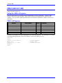
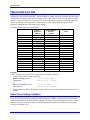
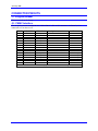
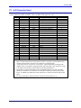
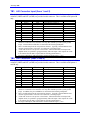
^1 USER MANUAL
^2 Accessory 28B
^3 16 Bit Analog to Digital Converter Board
^4 3Ax-602678-xUxx
^5 October 1, 2004
Single Source Machine Control
Power // Flexibility // Ease of Use
21314 Lassen Street Chatsworth, CA 91311 // Tel. (818) 998-2095 Fax. (818) 998-7807 // www.deltatau.com
Copyright Information
© 2003 Delta Tau Data Systems, Inc. All rights reserved.
This document is furnished for the customers of Delta Tau Data Systems, Inc. Other uses are
unauthorized without written permission of Delta Tau Data Systems, Inc. Information contained
in this manual may be updated from time-to-time due to product improvements, etc., and may not
conform in every respect to former issues.
To report errors or inconsistencies, call or email:
Delta Tau Data Systems, Inc. Technical Support
Phone: (818) 717-5656
Fax: (818) 998-7807
Email: [email protected]
Website: http://www.deltatau.com
Operating Conditions
All Delta Tau Data Systems, Inc. motion controller products, accessories, and amplifiers contain
static sensitive components that can be damaged by incorrect handling. When installing or
handling Delta Tau Data Systems, Inc. products, avoid contact with highly insulated materials.
Only qualified personnel should be allowed to handle this equipment.
In the case of industrial applications, we expect our products to be protected from hazardous or
conductive materials and/or environments that could cause harm to the controller by damaging
components or causing electrical shorts. When our products are used in an industrial
environment, install them into an industrial electrical cabinet or industrial PC to protect them
from excessive or corrosive moisture, abnormal ambient temperatures, and conductive materials.
If Delta Tau Data Systems, Inc. products are directly exposed to hazardous or conductive
materials and/or environments, we cannot guarantee their operation.
Accessory 28B
Table of Contents
INTRODUCTION .......................................................................................................................................................1
Options ......................................................................................................................................................................1
Input Offset Nulling ..................................................................................................................................................2
Things to Know.........................................................................................................................................................2
PMAC AND ACC-28B................................................................................................................................................3
Using Acc-28B in Programs......................................................................................................................................3
PMAC A-D Registers ............................................................................................................................................3
PMAC2 AND ACC-28B..............................................................................................................................................5
Phase Clock Setting Limitation .................................................................................................................................5
ACC-28B WITH ENCODER CONVERSION TABLE OPTIONS ON PMAC AND PMAC2............................7
Unsigned Analog Conversion ...................................................................................................................................7
Converted Data..........................................................................................................................................................7
Encoder Table Entry.............................................................................................................................................7
Encoder Table Usage.................................................................................................................................................7
Non-Turbo Example: ............................................................................................................................................7
Turbo Example: ....................................................................................................................................................8
LAYOUT DIAGRAM AND JUMPERS....................................................................................................................9
Layout Diagram-28B OPT 2A, Connectors and Jumpers .........................................................................................9
Layout Diagram Acc-28B OPT 2B, Connectors and Jumpers ..................................................................................9
Jumpers .....................................................................................................................................................................9
E1 - PMAC Ground ..............................................................................................................................................9
E2..........................................................................................................................................................................9
E3, E4 - PMAC/PMAC2 Select.............................................................................................................................9
E5, E6, E7, E8 - Unipolar/Bipolar Convert..........................................................................................................9
Jumper Table ......................................................................................................................................................10
CONNECTOR PINOUTS.........................................................................................................................................11
J1: Program Header.................................................................................................................................................11
J2: PMAC Interface................................................................................................................................................11
P1: A-D Converter Input ........................................................................................................................................12
TB1: A-D Converter Input (Axes 1 and 2).............................................................................................................13
TB2: A-D Converter (Axes 3 and 4) ......................................................................................................................13
TB3: Power Supply Input.......................................................................................................................................14
Table of Contents
i
Accessory 28B
ii
Table of Contents
Accessory 28B
INTRODUCTION
Delta Tau’s Accessory 28B (Acc-28B) is a 2 or 4-channel analog to digital converter interface board
(Option 1) designed to provide a means for precision voltage measurement as an input to PMAC and
PMAC2. This accessory uses four 16-bit analog-to-digital converters that provide voltage measurements
that are accurate to ±2 bits.
Jumpers will allow each A-D converter to be selected for Bipolar or Unipolar convert modes. When
selected for bipolar mode, differential inputs allow the user to apply input voltages to ±5V (10V p-p) and
single-ended inputs allow application of input voltages to +10V. When selected for unipolar mode,
differential inputs allow the application of input voltages from 0V to 5V and single-ended inputs allow
the application of input voltages from 0V to +10V. In unipolar mode, negative input voltages will not
damage the A-D converters.
Voltage references are provided for ratiometric style input control. The VREF output is provided for
equipment which uses a scaled input for accurate tracking. The +5Vdc and -5Vdc supply taps are less
precise and are provided to allow bias potentiometers to be biased without the need for an external power
supply.
Other features include:
Input nulling trimmers are provided to allow for precise adjustment of input signals.
Opto-couplers are used to isolate the Acc-28B’s circuitry from the PMAC/PMAC2.
When used with PMAC or Acc-24P, each Acc-28B occupies four channels using the PMAC’s JS1 or
JS2 interface connector.
• When used with PMAC2, each Acc-28B occupies two channels and is connected to an Acc-8T at J2.
• When used with PMAC2, all four A-D conversions are simultaneous.
• When used with PMAC2, an Acc-8T accessory card is required for connection to signals that are
available on the JMACH connector.
• Acc-28B requires ±15Vdc.
• The Acc-28B comes with mating connectors and a 16-conductor 24” long ribbon cable.
•
•
•
When used with PMAC2, the Acc-28B uses the same serial data inputs as is used by digital current loop
devices. Therefore, the Acc-28B is not to be used on the same channel pairs as Acc-8K1, Acc-8K2, Acc8F, or other devices which utilize the strobed serial input data lines.
Options
The Acc-28B is available with the following options:
• Option 1: Additional two axes (makes Acc-28B into 4 axis system)
• Option 2A: 25-pin DSUB connector at P1.
• Option 2B: 10-pin terminal blocks at TB1 and TB2.
Note:
Select either option 2A or option 2B above.
Introduction
1
Accessory 28B
Input Offset Nulling
Input nulling is performed with the A-D inputs shorted together using Bipolar conversion. If the
equipment has output offsets, it is possible to adjust the VR1, VR2, VR3, and VR4 to zero the inputs.
The input voltage adjustment swing is limited to approximately 60mV.
To adjust nulling, be sure that the temperature has stabilized on the Acc-28B by powering it for about 20
minutes then applying zeroed inputs. Adjust VR1 for channel 1, VR2 for channel 2, VR3 for channel 3,
and VR4 for channel 4 for the desired readings on the A-D.
When selected for Bipolar conversion, a 0Vdc input should read a number around 32,768 on the A-D
input. When selected for Unipolar conversion, the input should be adjusted to 00.
Things to Know
PMAC performs a sequential conversion of one A-D converter channel at a time. PMAC2 performs a
simultaneous conversion of all A-D channels at the same time.
Jumpers E3 & E4 select whether the board is addressed by a PMAC or PMAC2, respectively.
Be sure to adjust the ADCLK frequency for 1.25MHz. The A-D converters on the ACC28B have a
maximum conversion rate of approximately 1.7MHz.
2
Introduction
Accessory 28B
PMAC AND ACC-28B
The A-D CLK jumpers must be adjusted for a conversion value of 1.22MHz. On the PMAC PC, place
jumper E98 into position 2-3.
Using Acc-28B in Programs
The Acc-28B operates by converting data and transmitting it serially to the PMAC. There are eight
registers which receive the serial data. These registers may be accessed directly by selection of MVariables. There are subtle addressing differences between PMAC and PMAC2. PMAC references are
shown here:
PMAC A-D Registers
PMAC 1
Turbo PMAC1
ADC #
M105->Y:$C006,8,16,U
M205->Y:$C007,8,16,U
M305->Y:$C00E,8,16,U
M405->Y:$C00F,8,16,U
M505->Y:$C016,8,16,U
M605->Y:$C017,8,16,U
M705->Y:$C01E,8,16,U
M805->Y:$C01F,8,16,U
M105->Y:$78006,8,16,U
M205->Y:$78007,8,16,U
M305->Y:$7800E,8,16,U
M405->Y:$7800F,8,16,U
M505->Y:$78106,8,16,U
M605->Y:$78107,8,16,U
M705->Y:$7810E,8,16,U
M805->Y:$7810F,8,16,U
1
2
3
4
5
6
7
8
Connection
Connect Acc-28Bs
J2 to PMAC’s JS1
Connect Acc-28Bs
J2 to PMAC’s JS2
On PMAC, M-Variables are ideal for passing the A-D values into programs. The following is an example
of a program that displays the value of A-D input #1 on an LCD display (Acc-12):
OPEN PLC1
CLEAR
DISPLAY 0,”A-D VALUE IS WHILE (0<1)
DISPLAY 14, 5.0, M105
ENDWHILE
CLOSE
PMAC and Acc-28B
“
; DISPLAY HEADER.
; CREATE LOOP.
; DISPLAY A-D DATA.
3
Accessory 28B
4
PMAC and Acc-28B
Accessory 28B
PMAC2 AND ACC-28B
The A/D clock must be adjusted to operate at 1.25MHz. On PMAC2 models, this is accomplished by
adjusting the value of I903 and/or I907. On Turbo PMAC2 models, adjust the A/D clock with the I7m03
variable (where m stands for the Servo IC number). If no other values of clock are to be adjusted on the
PMAC2, set I903/I907/I7m03 to a value of 2770. Refer to the PMAC2 Software Addendum manual for
details on setting the I903 and/or I907 variables and refer to the Turbo PMAC/PMAC2 Software
Reference Manual for the details of the I7m03 setting.
The PMAC2 A-D registers are listed below:
PMAC2
Hardware
Address
Turbo PMAC2
Memory
Address
Name
1st A-D Channel
2nd A-D Channel
3rd A-D Channel
4th A-D Channel
Y:$C005,8,16,U
Y:$C006,8,16,U
Y:$C00D,8,16,U
Y:$C00E,8,16,U
Y:$78005,8,16,U
Y:$78006,8,16,U
Y:$7800D,8,16,U
Y:$7800E,8,16,U
ADC1A
ADC1B
ADC2A
ADC2B
5th A-D Channel
6th A-D Channel
7th A-D Channel
8th A-D Channel
Y:$C015,8,16,U
Y:$C016,8,16,U
Y:$C01D,8,16,U
Y:$C01E,8,16,U
Y:$78015,8,16,U
Y:$78016,8,16,U
Y:$7801D,8,16,U
Y:$7801E,8,16,U
ADC3A
ADC3B
ADC4A
ADC4B
9th A-D Channel
10th A-D Channel
11th A-D Channel
12th A-D Channel
Y:$C025,8,16,U
Y:$C026,8,16,U
Y:$C02D,8,16,U
Y:$C02E,8,16,U
Y:$78105,8,16,U
Y:$78106,8,16,U
Y:$7810D,8,16,U
Y:$7810E,8,16,U
ADC5A
ADC5B
ADC6A
ADC6B
13th A-D Channel
14th A-D Channel
15th A-D Channel
16th A-D Channel
Y:$C035,8,16,U
Y:$C036,8,16,U
Y:$C03D,8,16,U
Y:$C03E,8,16,U
Y:$78115,8,16,U
Y:$78116,8,16,U
Y:$7811D,8,16,U
Y:$7811E,8,16,U
ADC7A
ADC7B
ADC8A
ADC8B
Example:
A PLC program must read the value from the third A-D channel (ADC2A).
1. Assign an M-variable to point to ADC2A:
M205->Y:$C00D,8,16,U
I903=2770
;For non-Turbo PMAC2
;Set Clock to 1.23 MHz
or
M205->Y:$7800D,8,16,U
I7003=2770
;For Turbo PMAC2
;Set Clock to 1.23 MHz
2. When referenced, M205 will equal the value in ADC2A. Save the M-variables after they have been
assigned.
Phase Clock Setting Limitation
When using the Acc-28B the user must be aware of certain limitations. The first limitation is the ADC
clock rate. For this product, the maximum ADC clock rate is 1.2MHz. This leads to the next limitation
that is the maximum rate at which it can be sampled. The data is sampled during the phase clock. When
the phase clock goes from low to high, it is strobed and then the data must be latched by the time phase
clock goes from high to low.
PMAC2 and Acc-28B
5
Accessory 28B
PWM Counter
0
Ring/Phase
Clock
Strobe
Latch
The data from the ADC comes from a 24-bit register and each bit will be processed every ADC clock
cycle. Therefore, it will take a minimum of 24 ADC clock cycles to return the proper ADC value to the
PMAC. So, if we are limited to 1.2MHz ADC clock and it takes 24 cycles to read the data, then the
minimum of 20 µsec* is needed to read the data. The 20 µsec represents the time from the strobe to the
latch of the phase clock. To have a phase clock on time of about 20 µsec, set the phase clock to about 24
KHz. 24KHz is the maximum phase clock frequency that can be set in the PMAC2 when using Acc-28B.
*The 20 µsec is calculated by taking 1.2Mhz/24 cycles.
6
PMAC2 and Acc-28B
Accessory 28B
ACC-28B WITH ENCODER CONVERSION TABLE OPTIONS
ON PMAC AND PMAC2
The encoder conversion table can be modified using either PMAC’s Executive Program Encoder
Conversion Table dialog box or the on-line commands in Executive terminal mode.
The Encoder Conversion Table is used when motor position is desired from A-D inputs. Refer to the
PMAC Software User manual for Encoder Conversion Table uses and applications.
Unsigned Analog Conversion
The A-D converters on the Acc-28B return unsigned data to a PMAC or PMAC2.
If bit 19 of the analog conversion setup word is set to 1 ($18xxxx for normal analog), then
PMAC/PMAC2 treats the A-D number in the high 16 bits of the source word (left-justified of 24 bits) as
an unsigned number in the range of 0 to 65535.
Unsigned analog conversion requires PMAC or PMAC2 Firmware release Version 1.16 or newer to
accommodate unsigned A-D input values.
A typical setup word for this type of feedback is $18C005 for non-Turbo or $1F8005 for Turbo, which
provides for a non-filtered unsigned left-justified conversion of the data word fed by A-D #1 of the Acc28B connected to PMAC.
Converted Data
The converted data from the parallel word is put in the X data word of the encoder table entry. This
address is used by programs and PMAC pointers for the A-D value. For instance, if the first setup entry
(address Y:$0720) in the conversion table were $18C005, the result would be left-shifted at address
X:$720. For Turbo PMAC, if the first encoder conversion table entry (address Y:$003501) in the
conversion table were $1F8005, the result would be left-shifted at address X:$3501.
Encoder Table Entry
X-Words
Y-words
Latched data:
Unsigned 16 bit word
Source and process
Bits 0-15:
Address of source data
Bits 16-23:
= $18
Encoder Table Usage
Using the above table entry example, an encoder address may be set to point to the X memory side of the
table. This allows the sampling of data inside a servo/phase interrupt routine.
Non-Turbo Example:
The encoder table entry is placed at memory address Y:$0720 (as in previous converted data statement),
$18C006:
WY:$720,$18C006
The encoder address (Ix03, Ix04) is set to look at the converted result in the Encoder Table:
I103 = $720
Acc-28B with Encoder Conversion Table Options on PMAC & PMAC2
7
Accessory 28B
Turbo Example:
For the Turbo PMAC, set up the encoder conversion table with direct writes to the I-variables (ECT is
located at I8000 to I8191).
I8000=$1F8005
The encoder address (Ix03, Ix04) is set to look at the converted result in the encoder table:
I103 = $3501
For PMAC2 (optionally for PMAC), create an encoder table entry for each A-D input that is to be used.
On PMAC2, this is a requirement since the circuitry used for A-D conversion is not accessed
synchronously with a PLC program.
8
Acc-28B with Encoder Conversion Table Options on PMAC & PMAC2
Accessory 28B
LAYOUT DIAGRAM AND JUMPERS
0.125"
0.000"
4.775"
9.395"
Layout Diagram-28B OPT 2A, Connectors and Jumpers
0.125" DIA (typ)
0.125"
0.000"
PLACE SIP IN EITHER E3 OR E4
E3
PMAC1
E4
PMAC2
J2
E5
3
1
E7
1-2 UNIPOLAR
2-3 BIPOLAR
E1
3
1
E6
1-2 UNIPOLAR
2-3 BIPOLAR
1-2 UNIPOLAR
2-3 BIPOLAR
3
1
E8
1-2 UNIPOLAR
2-3 BIPOLAR
E2
3
TB3
1
VR3
VR2
VR4
P1
VR1
0.000"
4.675"
2.575"
2.700"
Layout Diagram Acc-28B OPT 2B, Connectors and Jumpers
PLACE SIP IN EITHER E3 OR E4
E3
PMAC1
E4
PMAC2
J2
E5
3
1
E7
1-2 UNIPOLAR
2-3 BIPOLAR
E1
3
1
E6
1-2 UNIPOLAR
2-3 BIPOLAR
1-2 UNIPOLAR
2-3 BIPOLAR
3
1
E8
1-2 UNIPOLAR
2-3 BIPOLAR
E2
3
TB3
1
VR2
TB1
VR3
VR4
TB2
VR1
Jumpers
Refer to the previous layout diagram for the location of the jumpers on the board. A position listing for
each jumper is provided in this section.
E1 - PMAC Ground
This jumper is used to connect PMAC’s ground to the power supply ground.
E2
Not used.
E3, E4 - PMAC/PMAC2 Select
This SIP jumper selects whether the Acc-28B is connected to PMAC or PMAC2. When connected to
PMAC, data conversion occurs one channel at a time. When connected to PMAC2, data is
simultaneously converted for all four channels.
E5, E6, E7, E8 - Unipolar/Bipolar Convert
These jumpers allow the selection of the method of A-D conversion for each channel. Position 1-2 allows
unipolar conversions, which returns an unsigned value of 0 to 65535 for input voltages ranging from 0 to
10V (approximately). Position 2-3 allows bipolar conversions, which return an unsigned value of 0 to
65535 for input voltages ranging from -10V to +10V (20V pk-pk).
Layout Diagram and Jumpers
9
Accessory 28B
Jumper Table
10
E Point
Pin
Layout
E1
1-2
E2
E3, E4
1-2-3
SIP socket
E5, E6,
E7, E8
1-2-3
Description
Default
Jumper pin 1 to 2 to connect the PMAC/PMAC2
power supply common to the supplied AGND.
Spare - unused jumper
Place the 10Ω SIP resistors in either socket
position.
E3 - PMAC1
E4 - PMAC2
Jumper pin 1 to 2 for Unipolar convert.
Jumper pin 2 to 3 for Bipolar convert.
E7 - Channel #1
E5 - Channel #2
E6 - Channel #3
E8 - Channel #4
1 to 2 on -100 boards;
Open on others
E3
2 to 3
Layout Diagram and Jumpers
Accessory 28B
CONNECTOR PINOUTS
J1: Program Header
This is used only at the factory.
J2: PMAC Interface
This 16-pin box header attaches the Acc-28B to PMAC’s JS1 or JS2 connector. On PMAC2, J2 is
connected to J2 on the Acc-8T.
Pin #
Symbol
Function
Description
Notes
1
DCLK
Input
A-D converter clock
2
n.c.
Not connected
3
ASEL0Input
PMAC address select
Not on PMAC2
4
ASEL1Input
PMAC address select
Not on PMAC2
5
CONV
Input
Start convert
6
ADCIN1
Output
PMAC serial data
Not on PMAC2
7
n.c.
Not connected
8
n.c.
Not connected
9
n.c.
Not connected
10
n.c.
Not connected
11
ADC0
Output
PMAC2 serial data Channel 1
PMAC2 only*
12
ADC1
Output
PMAC2 serial data Channel 2
PMAC2 only*
13
ADC2
Output
PMAC2 serial data Channel 3
PMAC2 only*
14
ADC3
Output
PMAC2 serial data Channel 4
PMAC2 only*
15
+5V
PMAC/PMAC2 +5V
16
GND
PMAC/PMAC2 GND
*These terminals are disconnected when jumper E3 is selected (PMAC1 configuration).
Connector Pinouts
11
Accessory 28B
P1: A-D Converter Input
This 25-pin DSUB contains the inputs and reference outputs for the ACC28B. The reference taps are
±5Vdc, 4.096Vdc (VREF) and RET. This is available with Option 2A only.
Pin #
Symbol
Function
Description
Notes
1
ADC1+
Input
A-D converter channel 1+
2
ADC1Input
A-D converter channel 15
3
ADC2+
Input
A-D converter channel 2+
4
ADC2Input
A-D converter channel 25
5
ADC3+
Input
A-D converter channel 3+
1
6
ADC3Input
A-D converter channel 31, 5
7
ADC4+
Input
A-D converter channel 4+
1
8
ADC4Input
A-D converter channel 41, 5
9
n.c.
10
n.c.
11
VREF
Output
4.096Vdc precision reference
2
12
+5Vdc
Output
+5V reference output
3
13
-5Vdc
Output
-5V reference output
3
14
SHIELD
Gnd
Shield
4
15
SHIELD
Gnd
Shield
4
16
SHIELD
Gnd
Shield
4
17
SHIELD
Gnd
Shield
4
18
SHIELD
Gnd
Shield
4
19
SHIELD
Gnd
Shield
4
20
SHIELD
Gnd
Shield
4
21
SHIELD
Gnd
Shield
4
22
n.c.
Not connected
23
n.c.
Not connected
24
RET
Gnd
VREF return
4
25
RET
Gnd
4
±5Vdc return
1. These signals exist on Option 1 (4-channel) boards only.
2. This is a buffered tap from the A-D precision reference. Typically, external hardware that
uses this signal reference will scale it for a full-scale A-D voltage input.
3. +5Vdc and -5Vdc are a less precise A-D reference. When used with an A-D input in the
unipolar mode, it is possible to get approximately full-scale inputs. This requires the -5Vdc
to be connected to the ADCx- input (ideal for metering potentiometers).
4. The shields are connected internally to the ground plane inside the Acc-28B. Normally,
shields are connected at one end of the wire only (this eliminates possible system ground
loops). In addition, the VREF and ±5Vdc return lines are connected to the internal ground
plane.
5. For single-ended inputs, ADCn should be connected to GND at pin24 or 25.
12
Connector Pinouts
Accessory 28B
TB1: A-D Converter Input (Axes 1 and 2)
This 10-pin terminal block contains the inputs for channel 1 and channel 2. Reference outputs of ±5Vdc,
4.096Vdc (VREF) and RET (AGND) are provided on this connector. This is available with Option 2B
only.
Pin #
Symbol
Function
Description
Notes
1
ADC1+
Input
A-D converter Channel 1+
2
ADC1Input
A-D converter Channel 14
3
AGND
Gnd
Shield
1
4
ADC2+
Input
A-D converter Channel 2+
5
ADC2Input
A-D converter Channel 24
6
AGND
Gnd
Shield
1
7
VREF
Output
4.096Vdc precision reference
2
8
AGND
Gnd
1
9
+5Vdc
Output
+5V reference output
3
10
-5Vdc
Output
-5V reference output
3
1. The shields are connected internally to the ground plane inside the Acc-28B. Normally,
shields are connected at one end of the wire only (this eliminates possible system ground
loops). Also the PIN 8 AGND line is connected to the internal ground plane.
2. This is a buffered tap from the A-D precision reference. Typically, external hardware that
uses this signal reference will scale it for a full-scale A-D voltage input.
3. +5Vdc and -5Vdc are a less precise A-D reference. When used with an A-D input in the
unipolar mode, it is possible to get approximately full-scale inputs. This requires the -5Vdc
to be connected to the ADCx- input (ideal for metering potentiometers).
4. For single-ended inputs, ADCn should be connected to GND at pin 3, 6 or 8.
TB2: A-D Converter (Axes 3 and 4)
This 10-pin terminal block contains the inputs for channel 3 and channel 4. Reference outputs of ±5Vdc,
4.096Vdc (VREF) and RET (AGND) are provided on this connector. This is available with Options 1
and 2B only.
Pin #
Symbol
Function
Description
Notes
1
ADC3+
Input
A-D converter Channel 3+
2
ADC3Input
A-D converter Channel 34
3
AGND
Gnd
Shield
1
4
ADC4+
Input
A-D converter Channel 4+
5
ADC4Input
A-D converter Channel 44
6
AGND
Gnd
Shield
1
7
VREF
Output
4.096Vdc precision reference
2
8
AGND
Gnd
1
9
+5Vdc
Output
+5V reference output
3
10
-5Vdc
Output
-5V reference output
3
1. The shields are connected internally to the ground plane inside the Acc-28B. Normally,
shields are connected at one end of the wire only (this eliminates possible system ground
loops). In addition, the pin 8 AGND line is connected to the internal ground plane.
2. This is a buffered tap from the A-D precision reference. Typically, external hardware that
uses this signal reference will scale it for a full-scale A-D voltage input.
3. +5Vdc and -5Vdc are a less precise A-D reference. When used with an A-D input in the
unipolar mode, it is possible to get approximately full-scale inputs. This requires the -5Vdc
to be connected to the ADCx- input (ideal for metering potentiometers).
4. For single-ended inputs, ADCn should be connected to GND at pin 3, 6 or 8.
Connector Pinouts
13
Accessory 28B
TB3: Power Supply Input
Pin #
1
2
3
4
1.
2.
14
Symbol
Function
Description
Notes
AGND
Common
Power supply return
N.C.
Not connected
+15Vdc
Input
+15V power input
1
-15Vdc
Input
-15V power input
2
+15Vdc requires a 200mA supply current. However, if the supply or reference taps at P1,
TB1 or TB2 are used and the current requirement may be greater.
-15Vdc requires 70mA supply current. However, if the supply taps at P1, TB1 or TB2 are
used and the current requirement may be greater.
Connector Pinouts