1
CONTENTS
CHAPTER 1 INTRODUCTION ...................................................................................................... 1
1.1 SOFTWARE DEVELOPMENT FLOW ................................................................................................ 1
1.2 SYSTEM REQUIREMENTS ............................................................................................................. 2
1.3 WHAT YOU WILL LEARN ............................................................................................................. 2
CHAPTER 2 CREATE AND BUILD YOUR PROJECT .............................................................. 3
2.1 CREATING A PROJECT FOLDER ..................................................................................................... 3
2.2 CREATING A DESIGN FILE ............................................................................................................ 3
2.3 CREATING THE MAKEFILE ........................................................................................................... 4
2.4 COMPILING THE PROJECT ............................................................................................................ 5
CHAPTER 3 EXECUTING YOUR PROJECT ............................................................................. 7
3.1 EXECUTE YOUR EXECUTABLE FILE ............................................................................................. 7
3.2 PUTTING MY_FIRST_HPS INTO THE BOOTABLE SD CARD ............................................................. 8
CHAPTER 4 APPENDIX ............................................................................................................... 11
4.1 HEADQUARTER & BRANCHES.................................................................................................... 11
DE0-Nano-SoC
My First FPGA Manual
i
www.terasic.com
May 18, 2015
Chapter 1
Introduction
This tutorial provides comprehensive information that will help you understand how to create a Clanguage software design and run it on your ARM-included DE0-Nano-SoC development board.
The following sections provide a quick overview of the design flow, explain what you need to get
started, and describe what you will learn.
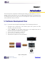
1.1 Software Development Flow
Figure 1-1 shows the software design flow block diagram. The development procedures are:
1.
Developers need to design their C-code software project with a generic text editor.
Generally, .c and .h files are needed.
2.
Create a “Makefile” for your software design project, so the compiler knows how to
generate a final object/executable files for your project.
Use the compile tool to generate executable file
Boot Linux from your DE0-Nano-SoC board.
Download the executable file to Linux and launch it.
3.
4.
5.
Figure 1-1 Design Flow
DE0-Nano-SoC
My First FPGA Manual
1
www.terasic.com
May 18, 2015
1.2 System Requirements
Besides the DE0-Nano-SoC board, the following software and hardware are required:
Microsoft Windows computer with USB port and Ethernet Port
Ethernet Router
Altera SoC EDS(Embedded Design Suite) software tool installed
Generic text editor tool installed
PuTTY installed
FTDI Virtual COM driver installed
A bootable SD card with the Linux system
1.3 W hat You W ill Lear n
In this tutorial you will perform the following tasks:
Create a "Hello World!" design that displays a message on the Linux terminal—This design is
easy to create and gives you visual feedback that the design works. Of course, you can use
your DE0-Nano-SoC board to run other designs as well.
Become familiar with Altera SoC EDS and Linux—This tutorial will not make you an expert,
but you should grasp some basic concepts about the compile tool and Linux operation in the
end of this tutorial.
DE0-Nano-SoC
My First FPGA Manual
2
www.terasic.com
May 18, 2015
Chapter 2
Create and Build Your Project
This chapter describes how to create your first HPS (Hard Processer System) project and build
(compile and link) it with the Altera SoC EDS software tool. We assume you have already installed
the Altera SoC EDS. If not, there are installatin details in Chapter 2 of the DE0-Nano-SoC Getting
Started Guide manual in the System CD.
2.1 Creating a Project Folder
A project usually includes the design files .c/.h and a make file. These files are generally stored
under the same folder. So, it is suggested to create a project folder where you can store your design
file and make file.
Developer can create a “my_first_hps” folder under the installed Altera SoC EDS installation
folder. From this point onward, the folder's absolute path will be assumed to be:
" C:\altera\14.1.0.186\embedded\my_first_hps ".
2.2 Creating a Design File
First, please create an empty file, named "main.c", under “my_first_hps” folder. Then, type below
code into the file and save it. The program includes the "stdio.h" header file for the "printf"
function, which is used to output a "Hello World!" message in a standard output device. By default,
the standard output device is the UART terminal.
#include <stdio.h>
int main(int argc, char **argv) {
printf("Hello World!\r\n");
DE0-Nano-SoC
My First FPGA Manual
3
www.terasic.com
May 18, 2015
return( 0 );
}
2.3 Creating the Makefile
A makefile is required for the Altera SoC EDS in order for it to know how to compile and link your
project. First, you will need to create an empty file, named “Makefile”, under “my_first_hps”
folder. Then, type in the following content and save it. Inside the makefile, the "TARGET" variable
defines the output file name. In this tutorial, the output executable file name is "my_first_hps". The
makefile also specifies which compiler to use, in this case we use ARM gcc cross compiler. The gcc
compile paramater "-I${SOCEDS_DEST_ROOT}/ip/altera/hps/altera_hps/hwlib/include" defines the
searching path for the gcc including header files.
#
TARGET = my_first_hps
#
CROSS_COMPILE = arm-linux-gnueabihfCFLAGS = -g -Wall -I
${SOCEDS_DEST_ROOT}/ip/altera/hps/altera_hps/hwlib/include
LDFLAGS = -g -Wall
CC = $(CROSS_COMPILE)gcc
ARCH= arm
build: $(TARGET)
$(TARGET): main.o
$(CC) $(LDFLAGS)
$^ -o $@
%.o : %.c
$(CC) $(CFLAGS) -c $< -o $@
.PHONY: clean
clean:
rm -f $(TARGET) *.a *.o *~
DE0-Nano-SoC
My First FPGA Manual
4
www.terasic.com
May 18, 2015
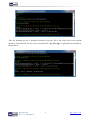
2.4 Compiling the Project
To compile a project, developers need to launch the Altera Embedded Command Shell first. Please
browse to the SoC EDS installation folder, e.g. "C:\altera\14.1\embedded", as shown in Figure 2-1.
Figure 2-1 Embedded Folder of SoC EDS
Then, double-click the "Embedded_Command_Shell.bat" item to launch Command Shell as shown
below.
In the Command Shell, please use the Linux “cd” command to change current directory to your
project folder. In this tutorial, just type “cd my_first_hps” to go to the project folder we just created.
Then, type a “make” command to start the building (compiling and linking) process, as shown
below.
DE0-Nano-SoC
My First FPGA Manual
5
www.terasic.com
May 18, 2015
After the building process is finished, developers can type "ls" to list all the files in the current
directory. In this tutorial, we can see the executable file “my_first_hps” is generated successfully as
shown below.
DE0-Nano-SoC
My First FPGA Manual
6
www.terasic.com
May 18, 2015
Chapter 3
Executing Your Project
This chapter describes how to execute your executable file “my_first_hps” on Linux on the
DE0-Nano-SoC board. Here, we assume you already know how to boot Linux on the
DE0-Nano-SoC board. For more details, please refer to Chapter 5 of the DE0-Nano-SoC Getting
Started Guide manual. We assumed you have installed the following softwares.
PuTTY
Virtual Com Driver
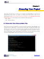
3.1 Execute Your Executable File
Before you can run your executable file, you need to copy the executable file “my_first_hps” to the
bootable SD card or USB storage, so you can access your file under a running Linux system on the
DE0-Nano-SoC board. If you have already put your executable file under the /home/root folder,
after logging in as a root user, you can type “./my_first_hps” to launch the executable file, and you
will see "Hello World!" on the UART terminal as shown below. If you don”t know how to put the
execute file “my_first_hps” into the SD card, please refer to the following section.
DE0-Nano-SoC
My First FPGA Manual
7
www.terasic.com
May 18, 2015
3.2 Putting my_first_hps into the bootable SD card
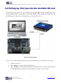
The section describes how to copy the executable file “my_first_hps” into the SD card using Linux
system command “scp”. First, you have to use an RJ45 cable to connect both your Windows PC and
the DE0-Nano-SoC board to your Ethernet router, as shown in Figure 3-1.
Figure 3-1 Ethernet Setup
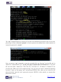
To boot Linux, follow the below procedure to get the Ethernet IP for your DE0-Nano-SoC board.
1.
Login as a root user
2.
3.
Type “udhcpc” to query an IP from DHCP server.
Type “ifconfig” to check the Ethernet IP for your DE0-Nano-SoC board. In this tutorial,
IP “192.168.1.113” is assigned to the DE0-Nano-SoC board, as shown below.
DE0-Nano-SoC
My First FPGA Manual
8
www.terasic.com
May 18, 2015
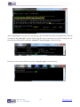
The “scp” command requires a password. If you have not defined the password for the root account,
please type in Linux command “passwd” to create a password, as shown below. In this tutorial, we
assume the password is “terasic”.
Now, you can use “scp” command to copy the executable file “my_first_hps” into the SD card. In
Altera SoC command shell, type “scp my_first_hps [email protected]:/home/root” to copy the
file into the folder “/home/root”. Note that, the "192.168.1.113" IP address is obtained in the
previous step. When you see the prompt message "Are you sure you want to continued connecting
(yes/no)?", reply yes by typing “yes” and pressing ENTER. Next, when you are asked for the
password, please enter the root's password and press ENTER. In this tutorial, we assumed the
password is “terasic”.
DE0-Nano-SoC
My First FPGA Manual
9
www.terasic.com
May 18, 2015
After completing the copy process, you can type “ls” to list the files in the current directory. We will
see that the “my_first_hps” appears. Before the file can be executed, you need to change the file
permission by running the command “chmod 777 my_first_hps” as shown below.
Finally, you can execute the file by typing “./my_first_hps” as shown below.
DE0-Nano-SoC
My First FPGA Manual
10
www.terasic.com
May 18, 2015
Chapter 4
Appendix
4.1 Headquar ter & Branches
Tel: +886-3-575-0880
Fax: +886-3-572-6690
Add: 9F, No.176, Sec.2, Gongdao 5th Rd, East Dist, Hsinchu City, Taiwan 300-70
Email: [email protected] / [email protected]
DE0-Nano-SoC
My First FPGA Manual
11
www.terasic.com
May 18, 2015