1
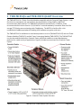
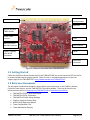
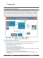
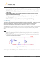
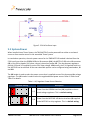
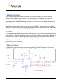
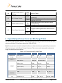
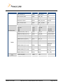
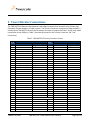
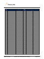
TWR-MCF51JG Tower Module User's Manual Rev. 1.1 Freescale Semiconductor Inc. TWRMCF51JGUM Table of Contents 1 TWR-MCF51JG and TWR-MCF51JG-KIT Overview .......................................................................4 1.1 Contents .................................................................................................................................................................................. 5 1.2 Features .................................................................................................................................................................................. 5 1.3 Getting Started ..................................................................................................................................................................... 6 1.4 Reference Documents ....................................................................................................................................................... 6 2 Hardware Description ...........................................................................................................................7 2.1 MCF51JG Microcontroller................................................................................................................................................ 7 2.2 Clocking .................................................................................................................................................................................. 8 2.3 System Power ....................................................................................................................................................................... 9 2.4 Debug Interface ................................................................................................................................................................ 13 2.4.1 OSBDM ................................................................................................................................................................................................. 13 2.5 Accelerometer ................................................................................................................................................................... 13 2.6 Pushbuttons, LEDs .......................................................................................................................................................... 14 2.7 General Purpose Tower Plug-in (TWRPI) Socket............................................................................................... 14 2.8 USB......................................................................................................................................................................................... 15 3 Jumper Table.......................................................................................................................................... 16 4 Input/Output Connectors and Pin Usage Table ......................................................................... 17 5 Tower Elevator Connections ............................................................................................................ 19 TWRMCF51JGUM TWR-MCF51JG Tower Module User's Manual Page 2 of 21 List of Figures Figure 1. Freescale Tower System Overview .............................................................................................. 4 Figure 2. Callouts on front side of the TWR-MCF51JG ............................................................................... 6 Figure 3. TWR-MCF51JG Block Diagram ..................................................................................................... 7 Figure 4. Main Oscillator Input ................................................................................................................... 8 Figure 5. 32 KHz Oscillator Input................................................................................................................. 9 Figure 6. Accelerometer Circuit ................................................................................................................ 13 Figure 7. USB dual-role interface .............................................................................................................. 16 List of Tables Table 1. J10, Regulator Power Source Selection......................................................................................... 9 Table 2. J9, Board Power Source Selection ............................................................................................... 11 Table 3. J12, Board Power Source Selection ............................................................................................. 11 Table 4. General Purpose TWRPI socket pinout ....................................................................................... 15 Table 5. TWR-MCF51JG Jumper Table ...................................................................................................... 16 Table 6. I/O Connectors and Pin Usage Table........................................................................................... 17 Table 7. TWR-MCF51JG Primary Connector Pinout .................................................................................. 19 Revision History Revision 0 1 TWRMCF51JGUM Date Oct. 2012 Changes Initial Release for Rev A pre-production module. Updates for Rev B module. TWR-MCF51JG Tower Module User's Manual Page 3 of 21 1 TWR-MCF51JG and TWR-MCF51JG-KIT Overview The TWR-MCF51JG is a Tower Controller Module compatible with the Freescale Tower System. It can function as a stand-alone, low-cost platform for the evaluation of the ColdFire+ MCF51JG microcontroller (MCU) devices. The TWR-MCF51JG features the MCF51JG, a ColdFire+ 32-bit microcontroller built on the Version 1 (V1) ColdFire® core and enabled by innovative 90nm thin film storage (TFS) flash process technology with FlexMemory. The MCF51Jx families offer a rich combination of additive peripherals including USB, hardware encryption, and more. The TWR-MCF51JG is available as a stand-alone product or as a kit (TWR-MCF51JG-KIT) with the Tower Elevator Modules (TWR-ELEV) and the Tower Prototyping Module (TWR-PROTO). The TWR-MCF51JG can also be combined with other Freescale Tower peripheral modules to create development platforms for a wide variety of applications. Figure 1 provides an overview of the Freescale Tower System. Figure 1. Freescale Tower System Overview TWRMCF51JGUM TWR-MCF51JG Tower Module User's Manual Page 4 of 21 1.1 Contents The TWR-MCF51JG contents include: TWR-MCF51JG board assembly 3ft A to mini-B USB cable for debug interface and power 3ft A to micro-B USB cable for MCF51JG USB interface Micro-A to A adapter for MCF51JG USB Host applications Quick Start Guide The TWR-MCF51JG-KIT contains: TWR-MCF51JG MCU module TWR-ELEV – Primary and Secondary Elevator Modules TWR-PROTO – Prototyping module 1.2 Features Figure 2 shows the TWR-MCF51JG with some of the key features called out. The following list summarizes the features of the TWR-MCF51JG Tower MCU Module: Tower compatible microcontroller module MCF51JG256: MCF51JG with 256 Kbytes of flash in a 44-pin MAPLGA package Dual role USB interface with Micro-AB USB connector General purpose Tower Plug-in (TWRPI) socket On-board debug circuit (OSBDM) with virtual serial port Three axis accelerometer (MMA8451Q) Two (2) user-controllable LEDs Two (2) user pushbutton switches & One (1) reset pushbutton switch TWRMCF51JGUM TWR-MCF51JG Tower Module User's Manual Page 5 of 21 MMA8451Q Accelerometer Primary Connector Switches General Purpose TWRPI Socket Power Select Jumpers LEDs MCF51JG MicroAB USB Connector MCF51JG256 Power / OSBDM Mini-B USB Connector Reset Secondary Connector Figure 2. Callouts on front side of the TWR-MCF51JG 1.3 Getting Started Follow the Quick Start Guide found printed in the TWR-MCF51JG box or the interactive DVD for the list of recommended steps for getting started. Check for new or revised documentation on the tool support page for the TWR-MCF51JG: http://www.freescale.com/TWR-MCF51JG. 1.4 Reference Documents The documents listed below should be referenced for more information on the ColdFire+ devices, Freescale Tower System, and the TWR-MCF51JG Controller Module. These can be found in the documentation section of freescale.com/TWR-MCF51JG or freescale.com/coldfire+. TWR-MCF51JG-QSG: Quick Start Guide TWR-MCF51JG-SCH: Schematics TWR-MCF51JG-PWA: Design Package ColdFire+ Portfolio Product Brief MCF51JG256 Reference Manual Tower Configuration Tool Tower Mechanical Drawing TWRMCF51JGUM TWR-MCF51JG Tower Module User's Manual Page 6 of 21 2 Hardware Description The TWR-MCF51JG is a Tower Controller Module featuring the MCF51JG256—a ColdFire+ based microcontroller with USB 2.0 full-speed OTG controllers in a 44 MAPLGA package. It is intended for use in the Freescale Tower System but can operate stand-alone. An on-board debug circuit, OSBDM, provides a BDM interface and a power supply input through a single USB mini B connector. Figure 3 shows a block diagram of the TWR-MCF51JG. The following sections describe the hardware in more detail. Figure 3. TWR-MCF51JG Block Diagram 2.1 MCF51JG Microcontroller The TWR-MCF51JG module features the MCF51JG256CFT. The key features of the microcontroller are: 32-bit ColdFire+ core with FlexMemory, EMAC, and DIV hardware acceleration 50 MHz maximum core operating frequency 44-pin MAPLGA, 5mm x 5mm 1.85V – 3.6V operating voltage input range 256 Kbytes of program flash, 64 Kbytes of static RAM FlexMemory consisting of 32 Kbytes of FlexMemory that can be used as additional non-volatile flash or up to 2KB of enhanced EEPROM. 10 flexible low power modes, ideal for extending battery life Cryptographic Acceleration Unit (CAU) and Random Number Generator (RNGA) for secure communications TWRMCF51JGUM TWR-MCF51JG Tower Module User's Manual Page 7 of 21 Integrated USB 2.0 Full-Speed Device/Host/OTG Controller supporting connection via USB and battery charging Serial audio interface (SAI) providing a direct interface to codecs and to Inter-IC Sound (I2S) audio devices Real-time debug support, with six hardware breakpoints that can be configured to halt the processor or generate debug interrupt Multi-purpose clock generator with PLL and FLL operation modes; multiple input oscillator or resonator frequency ranges; two internal trimmable references SPI, I2C, UART (SCI) GPIO with pin interrupt support, DMA request capability, digital glitch filtering 2.2 Clocking The ColdFire+ MCUs start up from an internal digitally controlled oscillator (DCO). Software can enable the main external oscillator (EXTAL/XTAL) if desired. The external oscillator/resonator for the Multipurpose Clock Generator (MCG) module can range from 32.768 KHz up to a 32 MHz. The TWR-MCF51JG provides an 8 MHz ceramic resonator as shown in Figure 4 below and sheet 4 of the schematics. This oscillator can be used as a clock source for the phase locked loop (PLL) inside the MCG. Notes 1. When R7 is not populated (default), configure the crystal oscillator for low-power operation (MCG_C2[HGO] = 0). 2. The resonator used here has internal load capacitors. Therefore no external or internal load capacitance within the MCU is required. Figure 4. Main Oscillator Input Additionally, the TWR-MCF51JG provides a 32.768 KHz oscillator for an accurate real time clock source. TWRMCF51JGUM TWR-MCF51JG Tower Module User's Manual Page 8 of 21 Figure 5. 32 KHz Oscillator Input 2.3 System Power When installed into a Tower System, the TWR-MCF51JG can be powered from either an on-board source or from another source in the assembled Tower System. In stand-alone operation, the main power source for the TWR-MCF51JG module is derived from the 5.0V input from either the OSBDM USB mini-B connector (J14), the MCF51JG USB micro-AB connector (J8), or the EzPort header (J16) when a shunt is placed on jumper J15. Two low-dropout regulators provide 3.3V and 2.0V supplies from the 5.0V input voltage. Additionally, the 3.3V regulator built into the MCF51JG can be selected. All the user selectable options can be configured using two headers, J9 and J10. The J10 header is used to select the power source that is supplied to one of the three possible voltage regulators. The J11 header is used to select the regulated board power source. Refer to Table 1 and Table 2 for details. Table 1. J10, Regulator Power Source Selection J10 Shunt Setting 2 Description 8 1 7 2 8 1 TWRMCF51JGUM 7 1-2 Power from the OSBDM interface (J14) supplied to the onboard voltage regulators. This is a default setting. 5-6 Power from the MCF51JG USB device interface (J8) supplied to the MCF51JG on-chip regulator. This is a default setting. TWR-MCF51JG Tower Module User's Manual Page 9 of 21 2 8 1 7 2 8 1 7 TWRMCF51JGUM 6-8 Power from the Tower Primary Connector USB device interface supplied to the MCF51JG on-chip regulator. 3-5 2-4 Power from the MCF51JG USB device interface (J8) supplied to the on-board voltage regulators. TWR-MCF51JG Tower Module User's Manual Page 10 of 21 Table 2. J9, Board Power Source Selection J9 Shunt Setting 2 Description 8 1 7 2 8 1 7 2 8 1 3-5 Board power is supplied by the 3.3V on-board (external) regulator. This is the default setting. 5-7 Board power is supplied by the 2.0V on-board (external) regulator. 1-2 Board power is supplied by the 3.3V MCF51JG on-chip (internal) regulator. 1-3 5-7 Power from the 3.3V MCF51JG on-chip (internal) regulator is supplied to the 3.3V on-board (external) regulator. Board power is supplied by the 2.0V on-board (external) regulator. Note: Take care not to install a shunt on J10 pins 1-2 when J9 is in this configuration. It is recommended to remove the shunt from J10 1-2 and use it on J9 for this setting. ― An external battery or other alternate source can be connected to pins 5 (positive) and 6 (negative, ground). 7 2 8 1 7 ― 2 + 1 8 7 The 3.3V or 2.0V power supplied to the MCU is routed through a jumper, J12. The jumper shunt can be removed to allow for either (1) selecting the source of the MCU supply voltage or (2) the measurement of power consumed by the MCU. Table 3. J12, Board Power Source Selection J12 Shunt Setting TWRMCF51JGUM Description 3-5 MCU power is supplied by the board power source selection jumper (J9). This is the default setting. 5-7 MCU power is supplied by the 3.3V MCF51JG on-chip (internal) regulator. Use this jumper setting if it is desired to power only the MCU with the on-chip (internal) regulator and not the rest of the board. TWR-MCF51JG Tower Module User's Manual Page 11 of 21 TWRMCF51JGUM TWR-MCF51JG Tower Module User's Manual Page 12 of 21 2.4 Debug Interface There are two debug interface options provided: the on-board OSBDM circuit and an external Background Debug Mode (BDM) connector. The BDM connector is a standard 6-pin connector providing an external debugger cable with access to the BDM interface of the MCF51JG256. Alternatively, the on-board OSBDM debug interface can be used to access the debug interface of the MCF51JG256. Note: When using an external debug pod to connect to the MCF51JG, be sure to connect the BDM cable to J17 (JG BDM). Avoid connecting to J18 (JM60 BDM) which is directly next to J17. J18 provides a debug connection to the OSBDM MCU (MC9S08JM60). 2.4.1 OSBDM An on-board MC9S08JM60 based Open Source BDM (OSBDM) circuit provides a BDM debug interface to the MCF51JG. A standard USB A male to mini-B male cable (provided) can be used for debugging via the USB connector, J14. The OSBDM interface also provides a USB to serial bridge. Drivers for the OSBDM interface are provided in the P&E Micro OSBDM/OSJTAG Tower Toolkit (available on the MCF51JG product website). These drivers and more utilities can be found online at http://www.pemicro.com/osbdm. 2.5 Accelerometer An MMA8451Q digital accelerometer is connected to the MCF51JG MCU through an I2C interface (I2C0: PTB2 and PTB3) and two GPIO/IRQ signals (PTC4 and PTC5). Figure 6. Accelerometer Circuit TWRMCF51JGUM TWR-MCF51JG Tower Module User's Manual Page 13 of 21 2.6 Pushbuttons, LEDs The TWR-MCF51JG features, two pushbutton switches (SW1 & SW2) connected to IRQ signals IRQ0 (PTB1) and IRQ3 (PTC1), a pushbutton switch (SW3) connected to the master reset signal, and two user-controllable LEDs connected to GPIO signals (PTB6 and PTC0). Refer to Table 6 “I/O Connectors and Pin Usage Table” for more information. 2.7 General Purpose Tower Plug-in (TWRPI) Socket The TWR-MCF51JG features a socket that can accept a variety of different Tower Plug-in modules featuring sensors, RF transceivers, and more. The General Purpose TWRPI socket provides access to I2C, SPI, IRQs, GPIOs, timers, analog conversion signals, TWRPI ID signals, reset, and voltage supplies. The pinout for the TWRPI Socket is defined in Table 4. Refer to Table 6 “I/O Connectors and Pin Usage Table” for the specific MCF51JG pin connections to the General Purpose TWRPI socket. TWRMCF51JGUM TWR-MCF51JG Tower Module User's Manual Page 14 of 21 Table 4. General Purpose TWRPI socket pinout Left-side 2x10 Connector Right-side 2x10 Connector Pin Description Pin Description 1 2 3 4 5 6 7 8 9 10 11 12 13 14 15 16 17 18 19 20 5V VCC 3.3 V VCC GND 3.3V VDDA VSS (Analog GND) VSS (Analog GND) VSS (Analog GND) ADC: Analog 0 ADC: Analog 1 VSS (Analog GND) VSS (Analog GND) ADC: Analog 2 VSS (Analog GND) VSS (Analog GND) GND GND ADC: TWRPI ID 0 ADC: TWRPI ID 1 GND Reset 1 2 3 4 5 6 7 8 9 10 11 12 13 14 15 16 17 18 19 20 GND GND I2C: SCL I2C: SDA GND GND GND GND SPI: MISO SPI: MOSI SPI: SS SPI: CLK GND GND GPIO: GPIO0/IRQ GPIO: GPIO1/IRQ GPIO: GPIO2 GPIO: GPIO3 GPIO: GPIO4/Timer GPIO: GPIO5/Timer 2.8 USB The MCF51JG features a USB full-speed/low-speed OTG/Host/Device controller with built-in transceiver. The TWR-MCF51JG routes the USB D+ and D- signals from the MCF51JG MCU to either the on-board USB connector (J8) or the Tower Primary Connector (allowing the connection to external USB connectors or additional circuitry on a Tower peripheral module) depending on the value of four optional resistors: R11/R12 and R13/R14. By default, R11 and R12 are not populated and R13 and R14 are. This connects the MCF51JG USB signals to the on-board USB circuit. A power supply switch with an enable input signal and over-current flag output signal is used to supply power to the USB connector when the MCF51JG is operating in host mode. Port pin PTA2 is connected to the flag output signal and port pin PTA1 is used to drive the enable signal. Both port pins can be isolated with jumpers if needed. TWRMCF51JGUM TWR-MCF51JG Tower Module User's Manual Page 15 of 21 Figure 7. USB dual-role interface 3 Jumper Table There are several jumpers on the TWR-MCF51JG that provide configuration selection and signal isolation. Refer to the following table for details. The default installed jumper settings are shown in bold with asterisks. Table 5. TWR-MCF51JG Jumper Table Jumper J1 J2 J4 J5 J9 Option USB Power Switch Enable Input Connection USB Power Switch Flag Output Connection SCI1/SPI1 Connection Selection SCI1/SPI1 Connection Selection Board Power Source Selection TWRMCF51JGUM Setting *ON* OFF *ON* OFF *1-2* 2-3 *1-2* 2-3 *3-5* Description Connect PTA1 to USB power switch enable input Disconnect PTA1 from USB power switch enable Connect PTA2 to USB power switch over-current flag output Disconnect PTA2 from USB power switch overcurrent flag output Connect SCI1_RX/SPI1_MISO to SPI1_MISO on Primary Edge Connect SCI1_RX/SPI1_MISO to SCI1_RX (RXD1) on Primary Edge Connect SCI1_TX/SPI1_MOSI to SPI1_MOSI on Primary Edge Connect SCI1_TX/SPI1_MOSI to SCI1_TX (TXD1) on Primary Edge Refer to Table 2 TWR-MCF51JG Tower Module User's Manual Page 16 of 21 J10 Regulator Power Source Selection *1-2* *5-6* *1-2* J12 MCU Voltage Selector 2-3 J13 ON OSBDM Mode Selection *OFF* ON J15 EzPort Power Connection *OFF* Refer to Table 1 Power MCU from board power source selection jumper (J9). Power MCU with output of on-chip voltage regulator (VOUT33). OSBDM bootloader mode (OSBDM firmware reprogramming) Debugger mode Connect on-board 5V supply to EzPort header (supports powering board from external EzPort probe) Disconnect on-board 5V supply from EzPort header 4 Input/Output Connectors and Pin Usage Table The following table provides details on which MCF51JG pins are using to communicate with the LEDs, switches, and other I/O interfaces onboard the TWR-MCF51JG. Note: Some port pins are used in multiple interfaces on-board and many are potentially connected to off-board resources via the Tower Primary Connector. Take care to avoid attempted simultaneous usage of mutually exclusive features. Table 6. I/O Connectors and Pin Usage Table Feature OSBDM/USB Bridge USB OTG EZPORT Switches SAI TWRMCF51JGUM Connection UART Receive UART Transmit Data Negative Data Positive EZPort Clock EZPort Data Out EZPort Data In EZPort Chip Select Reset SW1 SW2 SW3 SAI Receive FS Port Pin PTB5 PTB4 USB0_DN USB0_DP PTB0 PTA6 PTA7 PTB1 RESET_B PTB1 PTC1 RESET_B PTA6 Pin Function SCI2_RX SCI2_TX Differential Data Differential Data EZP_CLK EZP_DO EZP_DI EXP_CS_B JG_RESET_B IRQ0 IRQ3 Reset SAI0_RX_FS TWR-MCF51JG Tower Module User's Manual Shared With SPI2_MISO SPI2_MOSI TWRPI, USB OTG TWRPI, SAI TWRPI IRQ0/SW1 EZP_CS_B FTM1_CH5 EZPORT, TWRPI Page 17 of 21 Feature Accelerometer TWRPI LEDs TWRMCF51JGUM Connection SAI Transmit FS SAI Transmit Data SAI Receive Data Port Pin PTD0 PTD1 PTA5 SAI Receive Clock SAI Transmit Clock SAI Input Clock I2C Clock I2C Data IRQ1 IRQ2 TWRPI I2C SCL (J7 Pin 3) TWRPI I2C SDA (J7 Pin 4) TWRPI SPI MISO (J7 Pin 9) TWRPI SPI MOSI (J7 Pin 10) TWRPI SPI SS (J7 Pin 11) TWRPI SPI CLK (J7 Pin 12) TWRPI GPIO0 (J7 Pin 15) PTA3 PTD2 PTD3 PTB2 PTB3 PTC4 PTC5 PTB2 PTB3 PTC2 PTB7 PTC7 PTC3 PTA6 TWRPI GPIO1 (J7 Pin 16) TWRPI GPIO2 (J7 Pin 17) PTB0 PTA7 TWRPI GPIO3 (J7 Pin 18) PTA1 TWRPI GPIO4 (J7 Pin 19) Yellow LED (D5) Orange LED (D4) PTA2 PTB6 PTC0 Pin Function SAI0_RX_FS SAI0_TXD SAI0_RXD Shared With SPI SPI FTM1_CH4 FTM1_CH2, SAI0_RX_BCLK CLKOUT SAI0_TX_BCLK SPI SAI0_CLKIN/MCLK SPI IIC0_SCL IIC0_SDA IRQ1 SCI1_RTS IRQ2 SCI1_CTS IIC0_SCL Accelerometer IIC0_SDA Accelerometer SPI1_MISO SCI1_RX SPI1_MOSI SCI1_TX SPI1_SS SPI1_SCLK GPIO0 SAI0, EZPORT USB OTG, GPIO1 EZPORT GPIO2 EZPORT FTM1_CH0, GPIO3 IIC1_SCL FTM1_CH1, GPIO4 IIC1_SDA LED1 LED2 TWR-MCF51JG Tower Module User's Manual Page 18 of 21 5 Tower Elevator Connections The TWR-MCF51JG features two expansion card-edge connectors that interface to the Primary and Secondary Elevator boards in a Tower system. The Primary Connector (comprised of sides A and B) is utilized by the TWR-MCF51JG while the Secondary Connector (comprised of sides C and D) only makes connections to the GND pins. Table 7 provides the pinout for the Primary Connector. (NC = No Connection) Table 7. TWR-MCF51JG Primary Connector Pinout Pin # 1 2 3 4 5 6 7 8 9 10 11 12 13 14 15 16 17 18 19 20 21 22 23 24 25 26 27 28 29 30 31 32 33 Side B Name 5V GND 3.3V ELE_PS_SENSE_1 GND GND SDHC_CLK / SPI1_CLK NC SDHC_D3 / SPI1_CS0_b SDHC_CMD / SPI1_MOSI SDHC_D0 / SPI1_MISO NC NC NC NC NC NC NC NC NC GPIO1/UART1_RTS NC NC NC NC GND NC NC NC NC GND NC NC TWRMCF51JGUM Usage P5V_ELEV GND P3V3 ELE_PS_SENSE GND GND PTC3 PTC7 SPI1_MOSI SPI1_MISO PTC4 GND GND Pin # 1 2 3 4 5 6 7 8 9 10 11 12 13 14 15 16 17 18 19 20 21 22 23 24 25 26 27 28 29 30 31 32 33 Side A Name 5V GND 3.3V 3.3V GND GND IIC0_SCL IIC0_SDA GPIO9/UART1_CTS NC NC NC NC NC NC NC NC NC NC NC I2S0_MCLK I2S0_DOUT_SCK I2S0_DOUT_WS I2S0_DIN0 I2S0_DOUT0 GND NC NC NC NC GND NC NC TWR-MCF51JG Tower Module User's Manual Usage P5V_ELEV GND P3V3 P3V3 GND GND PTB2 PTB3 PTC5 PTD3 PTD2 PTD0 PTA5 PTD1 GND GND Page 19 of 21 Pin # 34 35 36 37 38 39 40 41 42 43 44 45 46 47 48 49 50 51 52 53 54 55 56 57 58 59 60 61 62 63 64 65 66 67 68 69 70 71 72 73 74 75 75 77 Side B Name NC GPIO4 3.3V NC NC PWM5 PWM4 NC NC NC SPI0_MISO SPI0_MOSI SPI0_CS0_b NC SPI0_CLK GND I2C1_SCL I2C1_SDA GPIO5 NC NC IRQ_H IRQ_G NC NC NC NC IRQ_B IRQ_A NC NC GND NC NC NC NC NC NC NC NC NC NC NC NC TWRMCF51JGUM Usage PTB6 P3V3 PTC1 PTA6 PTD2 PTD1 PTD0 PTD3 GND PTA1 PTA2 PTC0 PTB1 PTB1 PTC1 PTC1 GND Pin # 34 35 36 37 38 39 40 41 42 43 44 45 46 47 48 49 50 51 52 53 54 55 56 57 58 59 60 61 62 63 64 65 66 67 68 69 70 71 72 73 74 75 75 77 Side A Name NC NC 3.3V NC PWM2 PWM1 PWM0 UART0_RX UART0_TX UART1_RX UART1_TX NC NC NC NC NC NC NC NC NC USB0_DN USB0_DP NC USB0_VBUS NC NC NC NC RSTIN_B RSTOUT_B CLKOUT0 GND NC NC NC NC NC NC NC NC NC NC NC NC TWR-MCF51JG Tower Module User's Manual Usage P3V3 PTA3 PTA2 PTA1 PTB5 PTB4 SCI1_RX SCI1_TX JG_ELEV_USB0_DN JG_ELEV_USB0_DP USB0_VBUS JG_RESET_B JG_RESET_B PTA3 GND Page 20 of 21 Pin # 78 79 80 81 82 TWRMCF51JGUM Side B Name NC NC NC GND 3.3V Usage GND P3V3 Pin # 78 79 80 81 82 Side A Name NC NC NC GND 3.3V TWR-MCF51JG Tower Module User's Manual Usage GND P3V3 Page 21 of 21