1
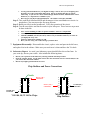
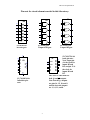
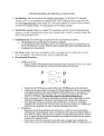
EE 2310 Laboratory Experiment #4: Laboratory Design Project
1. Introduction: In laboratory exercises 1-3, you became familiar with the basic circuit
elements. Today we will use these elements to design a more complex circuit.
2. Goal of this exercise: Familiarize students with the steps involved in doing a digital design.
We will go through most of these steps in order to complete a small design project.
3. Theory of experiment: In real world design projects there are always limitations on what
can be done during a given project, including power, size, cost, and performance, to name
just a few. Today’s project will focus on one of these limitations: number of pins. Your
design will be limited by the available inputs (switches) and outputs (LEDs) on the IDL-800
breadboard.
A typical digital design project may go through the following steps:
1.
2.
3.
Initial concept and specification
High level design and verification
Detailed design
4.
5.
6.
Simulation
Hardware implementation
Final testing
For today’s experiment, step 1 will be a given. You will complete steps 2,3,5, and 6. Since
our design is small, we will skip step 4 (which you would never do in the real world!). We
will rely on the final testing of our hardware to determine if our design is correct.
4. Experimental Equipment List: The following experimental components are required for
this experimental procedure:
•
•
•
IDL-800 circuit prototype unit and User Manual (as required)
Any of the devices in the digital logic kit
Breadboard wire connection kit
5. Pre-Work: Make sure you are up-to-date in all readings in Tokheim and the lecture
material. Although the circuit will be built in lab, you and your lab partner should proceed
through the design process and try to come to lab with a first-pass design.
6. Design Process: Today you will design an 8-bit adder, using SN 74LS83 4-bit adder
circuits. Your circuit will add two 8-bit numbers together (along with the carry in) and
display the result on the circuit-board LED’s. As there are only 8 input switches, you will
have to store one 8-bit input separately in order to provide the two inputs to the adder. Since
there are only 8 LED’s for the output, you will need to be creative and design a way to
display the carry out signal in addition to the sum bits. Some tips to help you get started:
•
•
•
You can only use the bank of 8 switches for the two inputs.
You can use the momentary switches to help you store the inputs, provide the carry in, etc.
Use the largest scale integration devices that you have. In other words, do not build a
register out of flip-flop chips. Use the SN 74LS75 4-bit registers in your kit to store data as
you are using the 74LS83 circuits as your 4-bit adder elements.
Step 1: Draw out your initial high-level design on paper (or with a CAD system such as
LogicWorks, if you purchased it). Verify that what you have drawn looks
conceptually correct. Some tips to help:
EE 2310: Experiment #4
•
Use large functional blocks for your high-level design. That is, since you are designing an 8bit adder, start with a single 8-bit adder block. It does not matter that there is no 8-bit
adder chip. As you move to a more detailed design, this block will be subdivided into actual
hardware (i.e., chips that are available to you).
Don’t forget your physical design limitations – the number of switches and LEDs.
•
Step 2: Take each large functional block and decompose it into actual hardware circuits. As
noted above, you can start on the first steps at home.
Step 3: Build your circuit on the breadboard. Verify the operation of the circuit.
Step 4: Test the cases below and list the results in your lab report. These last two steps must
be done in the lab.
•
•
•
Note: You are building an adder for positive numbers; NOT two’s complement.
Add 85 (01010101) and 42 (00101010) with no carry-in and then with carry-in.
Add 128 (10000000) and 127 (01111111) with no carry-in and then with carry-in. How do
you display the carry out?
Pick a few other binary numbers to add.
Have your TA verify your results and sign your data sheet.
•
•
7. Equipment Disassembly: Disassemble the circuit, replace wires and parts in the kit boxes,
and replace kits in the cabinet. Make sure your work area is clean and have the TA check.
8. Laboratory Report: As usual, your laboratory report should follow the on-line form. In
your write-up, discuss your results. Also include the following items:
•
•
•
Discuss your experience in the laboratory and any problems with the procedure.
Show the complete design. You do NOT need to show the connections to Power and Ground, nor do
you need to show the circuit outlines.
Discuss any insights gained from the exercises.
Chip Outlines and Power Connections
Notch
Notch
Ground (0V.)
connection
1
2
3
4
5
6
7
14
13
12
11
Power (+5V.)
connection
Power (+5V.)
connection
10
9
8
1
2
3
4
5
6
7
8
16
15
14
13
12
11
10
9
74LS83 & 74LS75
Chip Outlines
74 LS 04, 08, 32 14-Pin Chips
2
Ground (0V.)
connection
EE 2310: Experiment #4
Pin-outs for circuit elements needed in this laboratory:
32
08
04
13
12
11
10
9
8
5
6
3
4
1
2
3
1
2
3
4
5
6
4
5
6
9
10
8
9
10
8
12
13
11
12
13
11
1
2
SN 74LS08 Quad
SN 74LS32 Quad
inverter gate
2-input AND gate
2-input OR gate
14
SN 74LS04 Hex
16
4
7
11
B3
B2
B1
B0
A3
A2
A1
A0
83
4
15
S3 2
S2 6
S1 9
S0
13
7
6
3
2
CI
13
1
3
8
10
CO
SN 74LS83 4-bit
full adder pinouts.
3
SN 74LS75 4-bit
75
latch pin-outs –
Q3 8
Note: Input pin
11
23EN
Q2
14
4 is the clock for
Q1
01EN
Q0 1
inputs D3 and
9
D3
Q3
D4, and pin 13 is
Q2 10
D2
the clock for
Q1 15
D1
16
Q0
D0
inputs D1 and
D2.
The 74LS75 4-bit latch has
both Q and Q outputs.
Note that the Q outputs
are pins 16, 15, 10, and 9,
and the inverted outputs
are 1, 14, 11, and 8.