1
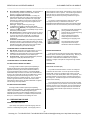
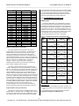
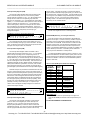
IOS-408
32-Channel Digital I/O Board
USER’S MANUAL
ACROMAG INCORPORATED
30765 South Wixom Road
P.O. BOX 437
Wixom, MI 48393-7037 U.S.A.
[email protected]
Copyright 2009, Acromag, Inc., Printed in the USA.
Data and specifications are subject to change without notice.
Tel: (248) 295-0310
Fax: (248) 624-9234
8500-841-B11C007
SERIES IOS-408 I/O SERVER MODULE
32-CHANNEL DIGITAL I/O MODULE
__________________________________________________________________________________________
The information contained in this manual is subject to change
without notice. Acromag, Inc. makes no warranty of any kind with
regard to this material, including, but not limited to, the implied
warranties of merchantability and fitness for a particular purpose.
Further, Acromag, Inc. assumes no responsibility for any errors that
may appear in this manual and makes no commitment to update,
or keep current, the information contained in this manual. No part
of this manual may be copied or reproduced in any form, without
the prior written consent of Acromag, Inc.
Table of Contents
1.0 GENERAL INFORMATION...........................................
KEY IOS-408 FEATURES.............................................
I/O SERVER MODULE INTERFACE FEATURES........
I/O SERVER MODULE SOFTWARE LIBRARY...........
2.0 PREPARATION FOR USE............................................
UNPACKING AND INSPECTION..................................
BOARD CONFIGURATION...........................................
CONNECTORS.............................................................
IOS Field I/O Connector (P2).....................................
I/O Noise and Grounding Considerations..................
Output Off-State Loading Considerations..................
3.0 PROGRAMMING INFORMATION.................................
ADDRESS MAPS..........................................................
IOS Digital Input Registers A & B..............................
IOS Digital Output Registers A & B...........................
Interrupt Enable Register...........................................
Interrupt Type Configuration Register........................
Interrupt Polarity Register..........................................
Interrupt Status Register............................................
Interrupt Vector Register...........................................
IOS Identification PROM...........................................
IOS-408 PROGRAMMING CONSIDERATIONS............
Programming Interrupts............................................
4.0 THEORY OF OPERATION............................................
INPUT/OUTPUT............................................................
5.0 SERVICE AND REPAIR................................................
SERVICE AND REPAIR ASSISTANCE........................
PRELIMINARY SERVICE PROCEDURE......................
WHERE TO GET HELP…………………………………..
6.0 SPECIFICATIONS.........................................................
GENERAL SPECIFICATIONS.......................................
DIGITAL INPUTS..........................................................
DIGITAL OUTPUTS......................................................
OUTPUT MOSFETS.....................................................
DRAWINGS
IOS-408 BLOCK DIAGRAM..........................
IOS-408 EXAMPLE OUTPUT CONNECTIONS
IOS-408 EXAMPLE INPUT CONNECTIONS..
Page
2
2
3
3
3
3
3
3
4
4
4
4
4
5
5
5
5
6
6
6
6
7
7
8
8
9
9
9
9
10
10
10
10
10
Page
11
12
12
IMPORTANT SAFETY CONSIDERATIONS
It is very important for the user to consider the possible adverse
effects of power, wiring, component, sensor, or software failures in
designing any type of control or monitoring system. This is
especially important where economic property loss or human life is
involved. It is important that the user employ satisfactory overall
system design. It is agreed between the Buyer and Acromag, that
this is the Buyer's responsibility.
1.0 GENERAL INFORMATION
The I/O SERVER MODULE (IOS) Series IOS-408 module is a
32-channel combination digital input/output board. This model
supports both 0 to 60V DC inputs, and 60VDC low-side switch
outputs, in any combination up to 32 channels. Four units mounted
on a carrier board provide up to 128 I/O points per 6U-VMEbus
system slot. As a combination input/output module, input channels
on this model can be used for “loopback” monitoring of the output
channel states. Up to 8 input channels can be programmed to
generate Change-Of-State (COS), Low, or High level transition
interrupts. The IOS-408 utilizes state of the art Surface-Mounted
Technology (SMT) to achieve its high channel density and is an
ideal choice for a wide range of industrial control and monitor
applications that require high-density, high-reliability, and highperformance at a low cost.
The IOS-408 standard temperature range is (-40oC to +85oC).
Important Note: The following IOS model are accessories to the
IOS Server Models: IOS-7200, IOS-7200-WIN, IOS-7400, and IOS7400-WIN; which are cULus Listed. This equipment is suitable for
use in Class I, Division 2, Groups A, B, C, and D or non-hazardous
locations only.
KEY IOS-408 FEATURES
High Channel Count - Interfaces with up to 32 input/output
points. Four units mounted on a carrier board provide up to
128 input and/or output channels in a single system slot. Input
and output channels may be intermixed in any combination.
The input circuitry of a single channel can also be used to
monitor the output state of the same channel to efficiently
implement “loopback” output control.
TTL-Compatible Input Threshold - Input threshold is at TTL
levels and includes hysteresis.
Input Hysteresis - Buffered inputs include hysteresis for
increased noise immunity.
Programmable Change-of-State/Level Interrupts Interrupts are software programmable for any bit Change-OfState or level on up to 8 channels.
Loopback Output Control & Fault Diagnostics - Input and
output circuitry is connected in tandem to each I/O channel,
making it directly compatible for “loopback monitoring” of the
output channel states. This feature can also be used to
implement self-test or fault diagnosis, since inherent loopback
can be used to detect open output switches or shorts.
High Voltage Inputs & Outputs - Inputs and outputs are
rated to 60VDC. I/O channels are non-isolated and share a
common connection.
High Impedance Inputs - High impedance inputs minimize
loading of the input source and input current.
-2Acromag, Inc. Tel:248-295-0310 Fax:248-624-9234 Email:[email protected] http://www.acromag.com
SERIES IOS-408 I/O SERVER MODULE
32-CHANNEL DIGITAL I/O MODULE
__________________________________________________________________________________________
No Configuration Jumpers or Switches - All configuration is
performed through software commands with no internal
jumpers to configure or switches to set.
Power Up & System Reset is Failsafe - For safety, the
outputs are always OFF upon power-up and cleared after a
system reset. Unlike some competitive units, output gate
pulldowns are included to ensure that the outputs do not turn
on momentarily when output load power is applied with no
power to the IOS module.
True Logic - Outputs operate using True-Logic
(1=ON/SWITCH CLOSED, 0=OFF/SWITCH OPEN).
Low RdsON (0.2 Maximum)- Low output drain-to-source ON
resistance ensures TTL logic-low compatibility at high currents
and reduces power dissipation.
High Output Current - individual output channels may sink up
to 1A DC continuous (up to 10A total, all channels combined),
or 312mA DC (with all 32 channels ON). No deration of
maximum output current is required at elevated ambient
temperatures.
Conduction Cooled Module - I/O modules employ advanced
thermal technologies. A thermal pad and module cover wicks
heat away from the module and transfers the energy to a heat
spreading friction plate. Heat moves to the enclosure walls
where it is dissipated by the external cooling fins.
I/O SERVER MODULE INTERFACE FEATURES
High density - Single-size, IOS module footprint. Up to four
units may be mounted on a 6U VMEbus carrier board.
Local ID - Each IOS module has its own 8-bit ID PROM which
is accessed via data transfers in the "ID Read" space.
16-bit & 8-bit I/O - Channel register Read/Write is performed
through D16 or D08 (EO) data transfer cycles.
badly damaged or water stained, request that the carrier's agent be
present when the carton is opened. If the carrier's agent is absent
when the carton is opened and the contents of the carton are
damaged, keep the carton and packing material for the agent's
inspection.
For repairs to a product damaged in shipment, refer to the
Acromag Service Policy to obtain return instructions. It is
suggested that salvageable shipping cartons and packing material
be saved for future use in the event the product must be shipped.
This board is physically protected with
packing material and electrically
protected with an anti static bag during
shipment. However, it is
recommended that the board be
visually inspected for evidence of
mishandling prior to applying power.
The board utilizes static sensitive
components and should only be
handled at a static-safe workstation.
BOARD CONFIGURATION
I/O SERVER MODULE SOFTWARE LIBRARY
Power should be removed from the board when installing IOS
modules, cables, termination panels, and field wiring. Refer to your
IOS module documentation for configuration and assembly
instructions. Model IOS-408 I/O Boards have no jumpers or
switches to configure--interrupts are configured through software
command.
IOS MODULE Win32 DRIVER SOFTWARE
CONNECTORS
Acromag provides a software product (sold separately) to
facilitate the development of Windows Embedded Standard
applications interfacing with I/O Server Modules installed on
Acromag Industrial I/O Server systems. This software (Model
IOSSW-DEV-WIN) consists of a low-level driver and Windows 32
Dynamic Link Libraries (DLLS) that are compatible with a number
of programming environments including Visual C++, Visual
Basic.NET, Borland C++ Builder and others. The DLL functions
provide a high-level interface to the IOS carrier and modules
eliminating the need to perform low-level reads/writes of registers,
and the writing of interrupt handlers.
IOS Field I/O Connector (P2)
IOS MODULE LINUX SOFTWARE
Acromag provides a software product (sold separately)
consisting of Linux software. This software (Model IOSSW-APILNX) is composed of Linux libraries designed to support
applications accessing I/O Server Modules installed on Acromag
Industrial I/O Server systems. The software is implemented as a
library of “C” functions which link with existing user code.
P2 provides the field I/O interface connector for mating IOS
modules to the carrier board. P2 is a 50-pin female receptacle
header (AMP 173279-3 or equivalent) which mates to the male
connector of the carrier board (AMP 173280-3 or equivalent). This
provides excellent connection integrity and utilizes gold-plating in
the mating area. The field and logic side connectors are keyed to
avoid incorrect assembly.
P2 pin assignments are unique to each IOS model (see Table
2.1) and correspond to the pin numbers of the front-panel, field-I/O
interface connector on the carrier board. The P2 pin assignments
of the IOS-408 I/O module correspond with those of the IOS-400
input module and the IOS-405 output module (for channels 0-31
and common).
2.0 PREPARATION FOR USE
UNPACKING AND INSPECTION
Upon receipt of this product, inspect the shipping carton for
evidence of mishandling during transit. If the shipping carton is
-3Acromag, Inc. Tel:248-295-0310 Fax:248-624-9234 Email:[email protected] http://www.acromag.com
SERIES IOS-408 I/O SERVER MODULE
32-CHANNEL DIGITAL I/O MODULE
__________________________________________________________________________________________
Table 2.1: IOS-408 Field I/O Pin Connections (P2)
Pin Description
OD00
OD01
OD02
OD03
OD04
OD05
OD06
OD07
OD08
OD09
OD10
OD11
OD12
OD13
OD14
OD15
OD16
OD17
OD18
OD19
OD20
OD21
OD22
OD23
OD24
Number
1
2
3
4
6
7
8
9
11
12
13
14
16
17
18
19
21
22
23
24
26
27
28
29
31
Pin Description
OD25
OD26
OD27
OD28
OD29
OD30
OD31
Not Used
Not Used
Not Used
Not Used
Not Used
Not Used
Not Used
Not Used
COMMON
COMMON
COMMON
COMMON
COMMON
COMMON
COMMON
COMMON
COMMON
COMMON
Number
32
33
34
36
37
38
39
41
42
43
44
46
47
48
49
5
10
15
20
25
30
35
40
45
50
I/O Noise and Grounding Considerations
The output channels of this model are the open drains of
mosfets with a common source connection. The IOS-408 is nonisolated between the logic and field I/O grounds since output
common is electrically connected to the IOS module ground.
Consequently, the field I/O connections are not isolated from the
carrier board and backplane. Two ounce copper ground plane foil
has been employed in the design of this model to help minimize the
effects of ground bounce, impedance drops, and switching
transients. However, care should be taken in designing
installations without isolation to avoid noise pickup and ground
loops caused by multiple ground connections.
This device is capable of switching many channels at high
currents. Additionally, the nature of the IOS interface is inherently
inductive. The outputs of this model are protected to voltages up to
60V. As such, when switching inductive loads, it is important that
careful consideration be given to the use of snubber devices to
shunt the reverse emf that develops when the current through an
inductor is interrupted. Filtering and bypassing at the load may also
be necessary. Additionally, proper grounding with thick conductors
is essential. Interface cabling and ground wiring should be kept as
short as possible. For outputs, the use of an interposing relay may
also be desireable for isolating the load, raising the drive capability,
or providing additional system protection. Please refer to IOS-408
Example Output Connections & Ios-408 Example Input
Connections diagram at the end of this manual for examples of
these connections and proper output and grounding connections.
Output Off-State Loading Considerations
With respect to output control, the 100K input buffer currentlimiting resistors in combination with +4.7V voltage clamps will tend
to increase the off-state drain current with increased drain voltage
(up to 0.5mA at 60V). This is due to the fact that the input buffer
circuitry and output mosfet drain circuitry are connected in tandem
to the same I/O pin. If this presents a problem for your application,
then you should consider separating the inputs and outputs by
using other IOS modules like the Acromag IOS-400 40-channel
input board and the IOS-405 40-channel output board.
3.0 PROGRAMMING INFORMATION
ADDRESS MAPS
This board is addressable in the Industrial Pack I/O space to
control the ON/OFF states of individual low-side switches and/or
the acquisition of digital inputs from the field. The I/O space may
be as large as 64, 16-bit words (128 bytes), but the IOS-408 only
uses a portion of this space. The I/O space address map for the
IOS-408 is shown in Table 3.1. Note the base address for the IOS
module I/O space (refer to the I/O Server manual) must be added
to the addresses shown to properly access the I/O space.
Accesses can be performed on an 8-bit or 16-bit basis.
Table 3.1: IOS-408 I/O Space Address (Hex) Memory Map
HIGH
LOW
Base
HIGH Byte
LOW Byte
Base
Addr.+
D15
D08
D07
D00
Addr.+
01
READ- Digital Input READ- Digital Input
Channel Register A Channel Register A
CH15
CH08 CH07
CH00 00
03
READ- Digital Input READ- Digital Input
Channel Register B Channel Register B
CH31
CH24 CH23
CH16 02
05
R/W -Digital Output R/W -Digital Output
Channel Register A Channel Register A
CH15
CH08 CH07
CH00 04
07
R/W - Digital Output R/W -Digital Output
Channel Register B Channel Register B
CH31
CH24 CH23
CH16 06
09
R/W - Interrupt
NOT DRIVEN
Enable Register1
CH07
CH00 08
0B
R/W -Interrupt Type
NOT DRIVEN
Config. Register1
CH07
CH00 0A
0D
R/W - Interrupt
NOT DRIVEN
Polarity Register1
CH07
CH00 0C
0F
R/W - Interrupt
NOT DRIVEN
Status Register1
CH07
CH00 0E
11
R/W - Interrupt
NOT DRIVEN
Vector Register1
10
13
12
NOT USED2
7F
7E
Notes (Table 3.1):
1. The upper 8 bits of this register are not driven. Pullups on the
carrier board data bus will cause these bits to always read high
(1‟s).
2. The IOS will not respond to addresses that are "Not Used".
IOS Digital Input Registers A & B (Read Only)
-4Acromag, Inc. Tel:248-295-0310 Fax:248-624-9234 Email:[email protected] http://www.acromag.com
SERIES IOS-408 I/O SERVER MODULE
32-CHANNEL DIGITAL I/O MODULE
__________________________________________________________________________________________
When the Digital Input Channel Data Registers are read, the
value read corresponds to the actual state of the input channels at
the time of the read. If the channel‟s tandem output mosfet is being
controlled and its drain is loaded, then reading the digital input
channel data register will return the state of the output (it is directly
connected to the drain). This is an efficient method of
accomplishing “loopback” control of the output. A “0” bit means
that the corresponding input signal is below the threshold value (or
the tandem output mosfet is ON), a “1” bit means that the
corresponding input signal is at or above the threshold value (or the
tandem mosfet is OFF and pulled up).
Thirty-two possible input channels numbered 0 through 31 may
be read. Channel read operations use 8-bit (D08(EO)), or 16-bit
(D16) data transfers with the lower ordered bits corresponding to
the lower-numbered channels for the register of interest (see
below). Register A monitors input channels 0 through 15. Register
B monitors input channels 16 through 31.
It is recommended that unused inputs not be left floating, but
pulled low by turning on the corresponding tandem output (see IOS
Digital Output Registers).
REGISTER B (OUTPUT SWITCHES 16 THROUGH 31):
MSB _ _ _ _ _ _ _
_ _ _ _ _ _ _ LSB
15 14 13 12 11 10 9 8
7 6 5 4 3 2 1 0
CH31.................................CH24 CH23...............................CH16
Each output channel register can be conveniently read back for
verification purposes. However, for critical control applications, it is
recommended that outputs be directly fed back to input points and
the input points monitored (loopback I/O). By design, input
channels are tied to the drains of the tandem output mosfet and a
read of the input channel register will return the inverse of a read of
the output channel register (a read of the input returns the drain
level, a read of the output returns the gate level). This is an
efficient method of accomplishing loopback output control without
requiring additional channels. However, this only applies for a
loaded drain (a pullup or other load connected to the drain).
All outputs are OFF (switch OPEN) following a power-on reset,
and are immediately cleared following a system reset. It is
recommended that unused outputs be turned on so that the
corresponding unused inputs are pulled low, rather than floating.
Interrupt Enable Register (R/W)
REGISTER A (INPUT CHANNELS 0 THROUGH 15):
MSB _ _ _ _ _ _ _
_ _ _ _ _ _ _ LSB
15 14 13 12 11 10 9 8
7 6 5 4 3 2 1 0
CH15...................... ............CH8 CH7..................................CH0
REGISTER B (INPUT CHANNELS 16 THROUGH 31):
MSB _ _ _ _ _ _ _
_ _ _ _ _ _ LSB
15 14 13 12 11 10 9 8
7 6 5 4 3 2 1 0
CH31..................................CH24 CH23............................CH16
IOS Digital Output Registers A & B (Read/Write)
When the Digital Output Channel Data Registers are written to,
the value written is represented at the corresponding output
channels. A “0” bit means that the corresponding output switch is
OPEN (OFF). Writing a “1” bit CLOSES the corresponding output
switch (turns it ON). There are two ways to accomplish an output
read. Reading the digital output channel register returns the state
configuration of this register (which is equivalent to the output
mosfet gate signal). Since input channels operate in tandem with
the output channels, reading the digital input channel register will
return the actual state of the output (it returns the level of the output
mosfet drain). That is, writing a „1‟ to an output turns the switch ON
(gate signal high). In turn, this drives the drain low (mosfet is
conducting). As such, a read of the input channel register will be
the inverse of a read of the output channel register for a loaded
output channel.
Read/Write Control for 32 output channels numbered 0 through
31 is provided. Channel state Read/Write operations use 8-bit
even or odd-byte, or 16-bit data transfers with the lower ordered bits
corresponding to the lower-numbered channels for the register of
interest (see below). Register A controls output channels 0 through
15. Register B controls output channels 16 through 31.
REGISTER A (OUTPUT SWITCHES 0 THROUGH 15):
MSB _ _ _ _ _ _ _
_ _ _ _ _ _ _ LSB
15 14 13 12 11 10 9 8
7 6 5 4 3 2 1 0
CH15..................................CH08 CH7..................................CH0
The digital input channel Interrupt Enable Registers provide a
mask bit for each of the 8 possible interrupt channels (channels 0-7
only). A “0” bit will prevent the corresponding input channel from
generating an external interrupt. A “1” bit will allow the
corresponding input channel to generate an interrupt. The unused
upper 8 bits of these 16-bit registers are “Don‟t Care” and will
always read high (1‟s) for D16 accesses.
INTERRUPT ENABLE REGISTER:
MSB _ _ _ _ _ _ _
_ _ _ _ _ _ _ LSB
15 14 13 12 11 10 9 8
7 6 5 4 3 2 1 0
X X X X X X X X CH7...................................CH0
All input channel interrupts are masked (“0”) following a reset.
Interrupt Type (COS or H/L) Configuration Register (R/W)
The Interrupt Type Configuration Registers determine the type
of input channel transition that will generate an interrupt for each of
the 8 possible interrupt channels (channels 0-7 only). A “0” bit
means that an interrupt will be generated when the input channel
level specified by the Interrupt Polarity Register occurs (i.e. Low or
High level transition interrupt). A “1” bit means the interrupt will
occur when a Change-Of-State (COS) occurs at the corresponding
input channel (i.e. any state transition). The unused upper 8 bits of
these 16-bit registers are “Don‟t Care” and will always read high
(1‟s) for D16 accesses. Note that interrupts will not occur unless
they are enabled.
INTERRUPT TYPE (COS or H/L) CONFIGURATION REGISTER:
MSB _ _ _ _ _ _ _
_ _ _ _ _ _ _ LSB
15 14 13 12 11 10 9 8
7 6 5 4 3 2 1 0
X X X X X X X X CH7..................................CH0
All bits are set to “0” following a reset which means that the
inputs will cause interrupts for the levels specified by the digital
input channel Interrupt Polarity Register.
-5Acromag, Inc. Tel:248-295-0310 Fax:248-624-9234 Email:[email protected] http://www.acromag.com
SERIES IOS-408 I/O SERVER MODULE
32-CHANNEL DIGITAL I/O MODULE
__________________________________________________________________________________________
Interrupt Polarity Register (R/W)
The Interrupt Polarity Register determines the level that will
cause a channel interrupt to occur for each of the 8 possible
interrupt channels (channels 0-7 only). A “0” bit specifies that an
interrupt will occur when the corresponding input channel is
BELOW TTL threshold (i.e. a “0” in the digital input channel data
register). A “1” bit means that an interrupt will occur when the input
channel is ABOVE TTL threshold (i.e. a “1” in the digital input
channel data register). Note that no interrupts will occur unless
they are enabled by the Interrupt Enable Register. Further, the
Interrupt Polarity Register will have no effect if the Change-of-State
(COS) interrupt type is configured by the Interrupt Type
Configuration Register.
INTERRUPT POLARITY (HIGH/LOW) REGISTER:
MSB _ _ _ _ _ _ _
_ _ _ _ _ _ _ LSB
15 14 13 12 11 10 9 8
7 6 5 4 3 2 1 0
X X X X X X X X CH7..................................CH0
The unused upper 8 bits of these 16-bit registers are “Don‟t
Care” and will always read high (1‟s) for D16 accesses. All bits are
set to “0” following a reset which means that the inputs will cause
interrupts when they are below TTL threshold.
Interrupt Status Register (R/W)
The Interrupt Status Register reflects the status of the 8
possible interrupt channels (channels 0-7 only). A “1” bit indicates
that an interrupt is pending for the corresponding channel. A
channel that does not have interrupts enabled will never set its
interrupt status flag. A channel‟s interrupt can be cleared by writing
a “1” to its bit position in the Interrupt Status Register (writing a “1”
acts as a reset signal to clear the set state). This is known as the
“Release On Register Access” (RORA) method, as defined in the
VME system architecture specification. However, if the condition
which caused the interrupt to occur remains, the interrupt will be
generated again (unless disabled via the Interrupt Enable Register).
Note that interrupts are prioritized via hardware within the card.
Channel 7 has the highest priority, channel 0 the lowest priority. If
multiple input channel interrupts become pending at the same time,
the vector corresponding to the highest numbered channel will be
delivered first. After the highest numbered channel‟s interrupt is
serviced and cleared, an additional interrupt will be generated for
the next highest priority channel with an interrupt pending. Note
that the input channel bandwidth should be limited to reduce the
possibility of missing channel interrupts. For a specific input
channel, this could happen if multiple changes occur before the
channel‟s interrupt is serviced.
INTERRUPT STATUS REGISTER:
MSB _ _ _ _ _ _ _
_ _ _ _ _ _ _ LSB
15 14 13 12 11 10 9 8
7 6 5 4 3 2 1 0
X X X X X X X X CH7...................................CH0
All interrupts are cleared following a reset.
Interrupt Vector Register (R/W)
The Interrupt Vector Register maintains an 8-bit interrupt
pointer for each of the 8 digital input channel interrupt lines
(channels 0-7 only). The lower 3 bits of the Interrupt Vector
Register (odd byte address) contain the channel number that
originated the interrupt. The upper 5 bits of the odd-addressed byte
are user-programmable and contain a pointer to the interrupt
service routine. Interrupts are served on a priority basis with the
higher numbered channels having higher priority (i.e. channel 7 has
the highest priority, channel 0 the lowest). The appropriate interrupt
vector is given to the VMEbus Interrupt Handler when an interrupt is
being serviced. As such, it is a pointer to 8 possible interrupt
handling routines. This allows each digital input channel to be
serviced by its own software handler.
INTERRUPT VECTOR REGISTER:
MSB _ _ _ _ _ _ _
_
_
_ _ _
15 14 13 12 11 10 9 8
7
6
5 4 3
X X X X X X X X User-Programmable
_ _ LSB
2
1 0
Channel No.
All bits of this register are set to “0” following a reset.
IOS ID PROM (Read Only, 32 even-byte addresses)
Each IOS module contains an identification (ID) PROM that
resides in the ID space. This area of memory contains 32 bytes of
information at most. Both fixed and variable information may be
present within the ID PROM. Fixed information includes the "IOS"
identifier, model number, and manufacturer's identification codes.
Variable information includes unique information required for the
module. The IOS-408 ID PROM does not contain any variable (e.g.
unique calibration) information. ID PROM bytes are addressed
using only the even addresses in a 64 byte block.
The IOS-408 ID PROM contents are shown in Table 3.2. Note
that the base-address for the IOS module ID space (refer to the I/O
Server manual) must be added to the addresses shown to properly
access the ID PROM. Execution of an ID PROM Read operation
requires 1 wait state.
Table 3.2: IOS-408 ID Space Identification (ID) PROM
Hex Offset
From ID
Numeric
PROM Base
Value
Address
(Hex)
Field Description
00
49
02
50
04
41
06
43
08
A3
Acromag ID Code
0A
03
IOS Model Code1
0C
00
Not Used
(Revision)
0E
00
Reserved
10
00
Not Used
12
00
Not Used
14
0C
Total Number of
ID ROM Bytes
16
C2
CRC
18 to 3E
00
Not Used
Notes (Table 3.2):
1. The IOS model number is represented by a two-digit code
within the ID PROM (the IOS-408 model is represented by 03
Hex).
IOS-408 PROGRAMMING CONSIDERATIONS
-6Acromag, Inc. Tel:248-295-0310 Fax:248-624-9234 Email:[email protected] http://www.acromag.com
SERIES IOS-408 I/O SERVER MODULE
32-CHANNEL DIGITAL I/O MODULE
__________________________________________________________________________________________
Programming Interrupts
Processing Change-of-State Interrupts:
Digital input channels can be programmed to generate
interrupts for the following conditions (channels 0-7 only):
Change-of-State (COS) at selected channels.
Input level (polarity) match at selected input channels.
Interrupts generated by the IOS-408 use interrupt request line
INTREQ0* (Interrupt Request 0). The interrupt release mechanism
employed is the Release On Register Access (RORA) type. This
means that the interrupter will release the I/O SERVER MODULE
interrupt request line (INTREQ0) after the interrupt has been
cleared by writing a “1” to the appropriate bit position in the input
channel Interrupt Status Register.
The Interrupt Vector Register contains information regarding
the interrupting channels. The lower 3 bits of this 8-bit number
contain the channel number of the interrupting channel. The upper
5 bits of this 8-bit number contain user-programmable information.
Interrupt service is prioritized with the higher numbered channel
having a higher priority over the lower numbered channels. Thus,
Channel 7 has the highest priority and channel 0 the lowest. As
such, if multiple channel interrupts become pending at the same
time, the pointer corresponding to the highest numbered channel
will be delivered first. After the highest numbered channel interrupt
is serviced and cleared, an additional interrupt will be generated for
the next highest priority (pending) interrupt.
When using interrupts, input channel bandwidth should be
limited to reduce the possiblity of missing channel interrupts. For a
given input channel, this could happen if multiple changes occur
before the channel‟s interrupt is serviced. The response time of the
input channels should also be considered when figuring this
bandwidth. The total response time is the sum of the input buffer
response time, plus the interrupt logic circuit response time, and
this time must pass before another interrupt condition will be
recognized.
The following programming examples assume that the IOS-408
is installed onto an Acromag I/O Server carrier board.
Interrupt Programming Example
1. Clear the Interrupt Enable Bits in the Carrier Board Status
Register by writing a "0" to bit 2 and bit 3.
2. Perform Specific IOS-408 Module Programming - see the
Change-of-State or Level (Polarity) Match programming examples
that follow, as required for your application.
3. Write a “1” to bit 2 of the Carrier Status/Control Register Module
Interrupt Enable bit to enable IOS module interrupts to the PCI bus.
Programming Example for Change-of-State Interrupts:
1. Select channel Change-of-State interrupts by writing a “1” to
each channel‟s respective bit in the Interrupt Type Register.
Note that Change-Of-State interrupts (specified with “1”) may be
mixed with polarity match interrupts (specified with “0”).
3. Enable individual input channel interrupts by writing a “1” to
each channel‟s respective bit in the Interrupt Enable Register.
4. Clear pending interrupts by writing a “1” to each channel‟s
respective bit in the Interrupt Status Register.
Change-of-State Interrupts may now be generated by the input
channels programmed above for any Change-Of-State
transition.
1. Clear the interrupting channel(s) by writing a “1” to the
appropriate bits in the IOS-408 Interrupt Status Register.
Programming Example for Level (Polarity) Match Interrupts:
1. Select channel Polarity Match Interrupts by writing a “0” to each
channel‟s respective bit in the Interrupt Type Register. Note that
Change-Of-State interrupts (specified with “1”) may be mixed
with Polarity Match Interrupts (specified with “0”).
3. Select the desired polarity (High/Low) level for interrupts by
writing a “0” (Low), or “1” (High) level to each channel‟s
respective bit in the Interrupt Polarity Register.
4. Enable individual input channel interrupts by writing a “1” to
each channel‟s respective bit in the Interrupt Enable Register.
5. Clear pending interrupts by writing a “1” to each channel‟s
respective bit in the Interrupt Status Register.
Interrupts can now be generated by matching the input level with
the selected polarity for programmed interrupt channels.
Processing Level (Polarity) Match Interrupts:
1. Disable the interrupting channel(s) by writing a “0” to the
appropriate bits in the IOS-408 Interrupt Enable Register.
2. After the interrupt stimulus has been removed, clear
the interrupting channel(s) by writing a “1” to the
appropriate bits in the IOS-408 Interrupt Status Register.
If the input stimulus is still applied, this will not clear
the Interrupt Status Register bit and the interrupting
channel(s) must remain disabled until the interrupt
stimulus has been removed. After removal of the input
stimulus the channel(s) may be cleared and re-enabled.
3. Re-enable the interrupting channel(s) by writing a “1” to
the appropriate bits in the Interrupt Enable Register.
General Sequence of Events for Processing an Interrupt
1. The IOS-408 asserts the Interrupt Request 0 Line (INTREQ0*)
in response to an interrupt condition at one or more inputs.
2. A generated interrupt is recognized by the carrier board and is
recorded in the carrier board‟s Interrupt Pending Register and
passed to the PCI bus by driving interrupt request signal INTA#
active.
3. The host processor uses the PCI interrupt to locate an interrupt
service routine to process interrupts from the carrier board.
4. The carrier board interrupt service routine examines the
carrier board‟s Interrupt Pending Register and invokes IOS
module interrupt service routines to service individual IOS modules.
3. The carrier board interrupt service routine accesses the
interrupt space of the IOS module selected to be serviced.
Note that the interrupt space accessed must correspond to
the interrupt request signal driven by the IOS module.
4. The carrier board will assert the INTSEL* signal to the
appropriate IOS module together with (carrier board generated)
address bit A1 to select which interrupt request is being
processed (A1 low corresponds to INTREQ0*; A1 high
corresponds to INTREQ1*).
5. The IOS module receives an active INTSEL* signal from the
carrier and supplies its interrupt vector to the host processor
during this interrupt acknowledge cycle. An IOS module
designed to release its interrupt request on acknowledge will
release its interrupt request upon receiving an active
INTSEL* signal from the carrier. If the IOS module is
designed to release it‟s interrupt request on register access
the interrupt service routine must also access the required
register to clear the interrupt request.
6. If the IOS module interrupt stimulus has been removed and
-7Acromag, Inc. Tel:248-295-0310 Fax:248-624-9234 Email:[email protected] http://www.acromag.com
SERIES IOS-408 I/O SERVER MODULE
32-CHANNEL DIGITAL I/O MODULE
__________________________________________________________________________________________
no other IOS modules have interrupts pending, the interrupt cycle
is completed (i.e. the carrier board negates its interrupt request
INTA#).
4.0 THEORY OF OPERATION
This section describes the basic functionality of the circuitry
used on the board. Refer IOS-408 BLOCK DIAGRAM as you
review this material.
INPUT/OUTPUT
The field I/O interface to the carrier board is provided through
connector P2 (refer to Table 2.1). Field I/O points are NONISOLATED. This means that the field return and logic common
have a direct electrical connection to each other. As such, care
must be taken to avoid ground loops (see Section 2 for connection
recommendations). Ignoring this effect may cause operation
errors, and with extreme abuse, possible circuit damage. Refer to
Ios-408 Example Output Connections & Ios-408 Example Input
Connections for example I/O and grounding connections.
A Field Programmable Gate Array (FPGA) is used to generate
all the logic necessary to operate the board. With respect to input
acquisition, the interrupt channels drive the FPGA through 8
individual buffers (channels 0-7 only). The input buffers of the other
24 channels are selectively enabled and drive the data bus directly.
The field input signals are tied to the inputs of these buffers via a
100K series connected resistor which limits the input current (but
raises the tandem output‟s off-state drain current). Additionally, the
buffer inputs are clamped to +4.7V (generated from the +12V
supply to minimize +5V loading). The input signal threshold is TTL
compatible. The typical threshold is 1.5V DC with 200mV of
hysteresis.
For output control, 32 open-drain outputs are connected in
tandem with 32 input buffers to each I/O channel. The outputs are
the open drains of individual mosfets. The gates of the mosfets are
driven by the FPGA. The sources of these mosfets are connected
in common. This configuration provides up to 32 low-side switches
for digital control. Writing a „1‟ to the output will turn the switch ON
(closed-circuit), a „0‟ will turn it OFF (open-circuit). Since the input
buffers are connected in tandem with the output mosfets, efficient
loopback monitoring of the output state can be accomplished by
reading the input channel registers.
With respect to output control, the 100K input buffer resistors
in combination with +4.7V voltage clamps will tend to increase the
off-state drain current with increased drain voltage (up to 0.5mA at
60V). This is due to the fact that the input buffer circuitry and
output mosfet drain circuitry are connected in tandem to the same
I/O pin. If this presents a problem for your application, then you
should consider separating the inputs and outputs by using other
boards like the Acromag IOS-400 40-channel input board and the
IOS-405
40-channel output board.
Output operation is considered „Fail-safe‟. That is, the outputs
are always OFF upon power-up reset, and are automatically
cleared following a system software reset. This is done for safety
reasons to ensure reliable control of the output state under all
conditions. Further, unlike some competitive units, output gate
pulldowns are included to ensure that the outputs do not turn on
momentarily when output load power is applied with no power to the
IOS module.
The output mosfets employed are rated for a much higher
current than specified. However, the field connector and cabling
used are only rated to 1A per pin (limiting a single channel to 1A).
For compatibility with other IOS models, 10 pins have been
reserved for ground return (hence; the 10A total current limitation
placed on this module). The low RdsON of the output mosfets will
ensure TTL-level compatible logic-low output signals even at high
(1A) output currents.
The output mosfets include an integrated zener diode between
the drain and the source. This provides output voltage clamp
protection to 60V. The tandem input channel is also rated to 60V.
However, when driving inductive loads such as relay coils, you
should always place a shunt diode across the load to shunt the
reverse EMF that develops across the coil when the current through
it is turned off (refer to Section 2 and see IOS-408 EXAMPLE
OUTPUT CONNECTIONS for an example of this type of
protection).
Since the input buffer and output mosfet circuitry share an I/O
pin, inputs and outputs may be intermixed in any combination.
Further, by providing an input channel for each output, efficient
loopback monitoring of the output state can be easily accomplished
(see IOS-408 EXAMPLE INPUT CONNECTIONS).
Digital input channels of this model can be configured to
generate interrupts for Change-Of-State (COS) and input level
(polarity) match conditions at selected input channels (channels 0-7
only). Interrupt service is prioritized with the higher numbered
channels having higher priority over the lower numbered channels.
An 8-bit interrupt service routine vector is provided during interrupt
acknowledge cycles on data lines D0...D7. The interrupt release
mechanism employed is RORA (Release On Register Access).
5.0 SERVICE AND REPAIR
SERVICE AND REPAIR ASSISTANCE
Surface-Mounted Technology (SMT) boards are generally
difficult to repair. It is highly recommended that a non-functioning
board be returned to Acromag for repair. The board can be
damaged unless special SMT repair and service tools are used.
Further, Acromag has automated test equipment that thoroughly
checks the performance of each board. When a board is first
produced and when any repair is made, it is tested, placed in a
burn-in room at elevated temperature, and retested before
shipment.
Please refer to Acromag's Service Policy Bulletin or contact
Acromag for complete details on how to obtain parts and repair.
PRELIMINARY SERVICE PROCEDURE
Before beginning repair, be sure that all of the procedures in
Section 2, Preparation For Use, have been followed. Also, refer to
the documentation of your carrier board to verify that it is correctly
configured. Verify that there are no blown fuses. Replacement of
the carrier and/or IOS with one that is known to work correctly is a
good technique to isolate a faulty board.
CAUTION: POWER MUST BE TURNED OFF BEFORE
REMOVING OR INSERTING BOARDS
-8Acromag, Inc. Tel:248-295-0310 Fax:248-624-9234 Email:[email protected] http://www.acromag.com
SERIES IOS-408 I/O SERVER MODULE
32-CHANNEL DIGITAL I/O MODULE
__________________________________________________________________________________________
WHERE TO GET HELP
If you continue to have problems, your next step should be to
visit the Acromag worldwide web site at http://www.acromag.com.
Our web site contains the most up-to-date product and software
information.
Go to the “Support” tab to access:
Application Notes
Frequently Asked Questions (FAQ‟s)
Product Knowledge Base
Tutorials
Software Updates/Drivers
An email question can also be submitted from within the Knowledge
Base or directly from the “Contact Us” tab.
Acromag‟s application engineers can also be contacted directly
for technical assistance via telephone or FAX through the numbers
listed below. When needed, complete repair services are also
available.
Phone: 248-295-0310
Fax: 248-624-9234
Email: [email protected]
6.0 SPECIFICATIONS
GENERAL SPECIFICATIONS
Operating Temperature................-40oC to +85oC
Relative Humidity..........................5-95% Non-Condensing.
Storage Temperature....................-55 C to +125 C.
Physical Configuration..................Single I/O SERVER MODULE .
Length................................... 4.030 in. (102.36 mm).
Width.....................................1.930 in. (49.02 mm)
Board Thickness....................0.062 in. (1.59 mm)
Height……………………........0.500 in. (12.7 mm)
Power:
+5 Volts ( 5%).......................13mA, Typical with outputs OFF;
28mA, Typical with outputs ON;
50mA Maximum.
+12 Volts ( 5%) from P1........7.3mA Typical; 8.5mA Maximum.
-12 Volts ( 5%) from P1.........0mA (Not Used)
Non-Isolated..................................Logic and field commons have a
direct electrical connection.
DIGITAL INPUTS
Input Channel Configuration.........32 non-inverting buffered inputs
with a common connection. For
DC voltage applications only,
observe proper polarity.
Input Signal Voltage Range...........0 to +60V DC, Maximum.
Input Signal Threshold..................TTL compatible. 1.5V DC with
200mV of hysteresis, typical.
Thus, Low-to-High threshold is
1.6VDC, High-to-Low is 1.4VDC,
typical. Limited to TTL levels of
0.8VDC (Max LOW level) and
2.0VDC (Min HIGH level).
Input Resistance...........................100K , Typical.
Input Hysteresis............................200mVDC centered at a 1.5VDC
threshold, Typical.
Input Current.................................560uA, Typical at 60VDC.
Interrupt Input Response Time......250nS minimum to 375nS
maximum, depending on when
the input transition occurs with
respect to the 8MHz clock.
Measured from input transition to
INTREQ0 line assertion.
DIGITAL OUTPUTS
Output Channel Configuration.......32 open-drain DMOS Mosfets
with common source connection.
For DC voltage applications only,
observe proper polarity.
Output “OFF” Voltage Range.........0 to +60V DC, Maximum.
Output “OFF” Leakage Current......25uA Maximum (Mosfet Only,
55 C, 48V). Does not include
tandem input bias current.
NOTE: The 100K input buffer
resistors in combination with
+4.7V voltage clamps will tend to
increase the off-state drain
current with increased drain
voltage (up to 0.5mA at 60V).
This is due to the fact that the
input buffer circuitry and output
mosfet drain circuitry are
connected in tandem to the same
I/O pin.
Output “ON” Current Range...........0 to +1A DC, continuous (up to
10A total for all channels
combined), or 300mA DC,
continuous (all channels ON).
No deration required at elevated
ambients.
Output Rds ON Resistance.............0.2 , Maximum (25 C).
Turn-ON Time................................Varies with load, 320ns Typical,
with 330 pull-up to +5V and
12-inch ribbon cable. Measured
from IOSEL line assertion to
output drain state transfer to TTL
0.8V level.
Turn-OFF Time..............................Varies with load, 500ns Typical,
with 330 pull-up to +5V and
12-inch ribbon cable. Measured
from IOSEL line assertion to
output drain state transfer to TTL
2.0V level.
Resistance to RFI...........................No digital upsets occur for field
strengths up to 10V per meter at
27MHz, 151MHz, & 460MHz per
SAMA PMC 33.1 test
procedures.
Resistance to EMI..........................Unit has been tested with no
digital upsets under the influence
of EMI from switching solenoids,
commutator motors, and drill
motors.
Surge Withstand Capability...........Outputs exhibit no damage when
tested with a standardized test
waveform representative of
surges (high frequency transient
electrical interference) per
ANSI/IEEE C37.90-1978.
-9Acromag, Inc. Tel:248-295-0310 Fax:248-624-9234 Email:[email protected] http://www.acromag.com
SERIES IOS-408 I/O SERVER MODULE
32-CHANNEL DIGITAL I/O MODULE
__________________________________________________________________________________________
ESD Protection..............................Outputs exhibit no degradation of
performance with repeated ESD
induced voltages to 6KV per
DOD-STD-1686.
OUTPUT MOSFETS
(These specifications are included for reference and apply to
the output driver only. See DIGITAL OUTPUTS above for
module specifications).
Manufacturer/Part Number............National NDS9945,
Siliconix Si9945DY.
Voltage VDSS..................................60V DC, Maximum.
Current ID.......................................3.5A, Continuous (25 C),
2.8A, Continuous (70 C).
ON Resistance RDS.......................0.2 (VGS=4.5V, 25 C).
Power Dissipation PD....................2W (25 C).
Output “OFF” Leakage Current....25uA Maximum (55 C, 48V).
- 10 Acromag, Inc. Tel:248-295-0310 Fax:248-624-9234 Email:[email protected] http://www.acromag.com
SERIES IOS-408 I/O SERVER MODULE
32-CHANNEL DIGITAL I/O MODULE
__________________________________________________________________________________________
- 11 Acromag, Inc. Tel:248-295-0310 Fax:248-624-9234 Email:[email protected] http://www.acromag.com
SERIES IOS-408 I/O SERVER MODULE
32-CHANNEL DIGITAL I/O MODULE
__________________________________________________________________________________________
- 12 Acromag, Inc. Tel:248-295-0310 Fax:248-624-9234 Email:[email protected] http://www.acromag.com