1
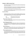
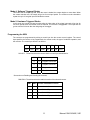
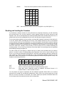
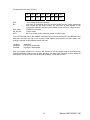
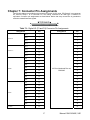
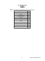
10623 Roselle Street, San Diego, CA 92121 y (858) 550-9559 y Fax (858) 550-7322
[email protected] y www.accesio.com
MODEL 104-DIO-48E
and 104-DIO-24E
USER MANUAL
FILE: M104-DIO-48E.A1n
Notice
The information in this document is provided for reference only. ACCES does not assume any liability arising
out of the application or use of the information or products described herein. This document may contain or
reference information and products protected by copyrights or patents and does not convey any license under
the patent rights of ACCES, nor the rights of others.
IBM PC, PC/XT, and PC/AT are registered trademarks of the International Business Machines Corporation.
Printed in USA. Copyright 2001, 2005 by ACCES I/O Products, Inc. 10623 Roselle Street, San Diego, CA
92121. All rights reserved.
WARNING!!
ALWAYS CONNECT AND DISCONNECT YOUR FIELD CABLING WITH THE
COMPUTER POWER OFF. ALWAYS TURN COMPUTER POWER OFF
BEFORE INSTALLING A BOARD. CONNECTING AND DISCONNECTING
CABLES, OR INSTALLING BOARDS INTO A SYSTEM WITH THE
COMPUTER OR FIELD POWER ON MAY CAUSE DAMAGE TO THE I/O
BOARD AND WILL VOID ALL WARRANTIES, IMPLIED OR EXPRESSED.
2
Manual 104-DIO-48E, 24E
Warranty
Prior to shipment, ACCES equipment is thoroughly inspected and tested to applicable specifications. However,
should equipment failure occur, ACCES assures its customers that prompt service and support will be available.
All equipment originally manufactured by ACCES which is found to be defective will be repaired or replaced
subject to the following considerations.
Terms and Conditions
If a unit is suspected of failure, contact ACCES' Customer Service department. Be prepared to give the unit
model number, serial number, and a description of the failure symptom(s). We may suggest some simple tests
to confirm the failure. We will assign a Return Material Authorization (RMA) number which must appear on the
outer label of the return package. All units/components should be properly packed for handling and returned
with freight prepaid to the ACCES designated Service Center, and will be returned to the customer's/user's site
freight prepaid and invoiced.
Coverage
First Three Years: Returned unit/part will be repaired and/or replaced at ACCES option with no charge for labor
or parts not excluded by warranty. Warranty commences with equipment shipment.
Following Years: Throughout your equipment's lifetime, ACCES stands ready to provide on-site or in-plant
service at reasonable rates similar to those of other manufacturers in the industry.
Equipment Not Manufactured by ACCES
Equipment provided but not manufactured by ACCES is warranted and will be repaired according to the terms
and conditions of the respective equipment manufacturer's warranty.
General
Under this Warranty, liability of ACCES is limited to replacing, repairing or issuing credit (at ACCES discretion)
for any products which are proved to be defective during the warranty period. In no case is ACCES liable for
consequential or special damage arriving from use or misuse of our product. The customer is responsible for all
charges caused by modifications or additions to ACCES equipment not approved in writing by ACCES or, if in
ACCES opinion the equipment has been subjected to abnormal use. "Abnormal use" for purposes of this
warranty is defined as any use to which the equipment is exposed other than that use specified or intended as
evidenced by purchase or sales representation. Other than the above, no other warranty, expressed or implied,
shall apply to any and all such equipment furnished or sold by ACCES.
3
Manual 104-DIO-48E, 24E
Table of Contents
Chapter 1: Introduction .........................................................................................................5
Specification ..................................................................................................................................................... 6
Figure 1-1: Block Diagram ............................................................................................................................ 7
Chapter 2: Installation ...........................................................................................................8
Figure 2-1: PC/104 Key Information ............................................................................................................. 9
Chapter 3: Option Selection ...............................................................................................10
Figure 3-1: Option Selection Map ............................................................................................................... 11
Chapter 4: Address Selection.............................................................................................12
Table 4-1: Standard Address Assignments for Computers......................................................................... 12
Table 4-2: Base Address Table................................................................................................................... 13
Chapter 5: Programming.....................................................................................................15
Developing Your Application Software........................................................................................................ 15
Table 5-1: Address Selection Table ............................................................................................................ 15
Digital I/O......................................................................................................................................................... 16
Table 5-2: Control Register Bit Assignment ................................................................................................ 16
Programming Example (Basic) ..................................................................................................................... 18
Enabling/ Disabling I/O Buffers .................................................................................................................... 18
Counter/Timer................................................................................................................................................. 19
Sharing Interrupts on the ISA Bus ............................................................................................................... 20
Chapter 6: 8254 Counter/Timer ..........................................................................................21
Operational Modes ......................................................................................................................................... 21
Reading and Loading the Counters ............................................................................................................. 23
8254 Driver ...................................................................................................................................................... 25
Enabling the Counter/Timer .......................................................................................................................... 26
Chapter 7: Connector Pin Assignments ............................................................................27
Table 7-1: Digital I/O (P3 and P4) Connector Pin Assignments ................................................................. 27
Table 7-2: Counter/Timer (82C54) Connector Pin Assignments ................................................................ 28
4
Manual 104-DIO-48E, 24E
Chapter 1: Introduction
Features
•
48 Bits of Digital Input/Output.
•
Software Controlled Interrupt Generation.
•
All 48 I/O Lines are Buffered on the Board.
•
I/O Buffers Can Be Enabled/Disabled under Program Control.
•
Four and Eight Bit Ports Independently Selectable for I/O.
•
Pull-Ups on I/O Lines are standard, Pull-downs are an option.
•
+5V Supply Available to the User (fused, resettable).
•
Compatible with Industry Standard I/O Racks like Gordos, Opto-22, Potter & Brumfield, etc.
•
Counter/Timer 82C54, 3x16 bit (optional).
Applications
•
Automatic Test Systems.
•
Laboratory Automation.
•
Robotics.
•
Machine Control.
•
Security Systems, Energy Management.
•
Relay Monitoring and Control.
•
Parallel Data Transfer to PC.
•
Sensing Switch Closures or TTL, DTL, CMOS Logic.
•
Driving Indicator Lights or Recorders.
Description
This board was designed for industrial applications and can be installed in a 16 bit or 8 bit PC/104 bus
socket. Each I/O line is buffered and capable of sourcing 32mA or sinking 64mA. The board contains
two Programmable Peripheral Interface (PPI) chips of type 82C55 to provide a computer interface to 48
I/O lines. There are three 8 bit ports: A, B, and C per PPI. Each 8 bit port can be configured by software
to function as either inputs or latched outputs. Port C can also be configured as four inputs and four
outputs. Pull-ups on the board assure that there are no erroneous outputs at power up. Pull-downs for
any port can be installed at the factory on request.
Also, bit C3 at each 24-bit Group can be used as an external interrupt to the computer. When bit C3
goes high (edge triggering), an interrupt may be requested. Interrupts from the ports are OR'ed
together. Interrupts are directed to levels #3 through #7 and #10 through #12 by jumper installation.
Jumpers allow interrupts from Port C bit 3 (either or both Groups) always, never, or controlled by Port C
bit 7.
Tristate I/O line buffers (74LS245) are configured automatically by hardware logic for input or output
according to direction assignment written to the control register in the PPI. Further, a jumper on the
board allows the tristate buffers to be enabled or disabled under program control. (See the Option
Selection section to follow.)
5
Manual 104-DIO-48E, 24E
I/O wiring connections are via 50-pin headers on the board. Two flat ribbon cables connect the board to
external devices. This provides compatibility with OPTO-22, Gordos, Potter & Brumfield, and all module
mounting racks. Every second conductor of the flat cables is grounded to minimize crosstalk between
signals. If needed for external circuits, +5 VDC power (resettable fuse) is available on pin 49 of each I/O
connector.
The board occupies sixteen bytes of I/O address space. The base address is selectable via jumpers
anywhere within the range of 000-3F0 hex. An illustrated setup program is provided with the board.
Interactive displays show locations and settings of jumpers to select the board address, interrupt levels,
and interrupt enables. Also, samples in several programming languages are presented in the Software
section of this manual and on the accompanying CD.
The board optionally has an 82C54 Counter/Timer chip. This can be used for frequency measurement,
frequency output, pulse width modulation, pulse width measurement, event count, etc.
SPECIAL NOTE FOR PROGRAMMERS:
The one language not recommended for programming interrupt service routines is any version of
Visual BASIC. The recommended programming languages for IRQ based applications are Delphi, C++
Builder, or Visual C.
Specification
Digital Inputs (TTL Compatible)
•
Logic High:
2.0 to 5.0 VDC.
•
Logic Low:
-0.5 to +0.8 VDC.
•
Input Load (Hi):
20 uA.
•
Input Load (Lo):
-200 uA.
Digital Outputs
•
Logic High:
2.5 VDC min., source 32 mA.
•
Logic Low:
0.5 VDC max., sink 64 mA.
•
Power Output:
+5 VDC from computer bus (ext. 0.5A fast-blow fuse is recommended).
•
Power Required:
+5 VDC at 50 mA typical (all outputs HIGH, depends on features installed)
Optional Counter/Timers
•
Type:
82C54 programmable interval counters
•
Output Drive:
8mA.
•
Input Gate:
TTL/CMOS compatible.
•
Clock Output:
1MHz crystal-controlled oscillator.
•
Active Count Edge:
Negative edge.
•
Timer Range:
16 bits event counter, 32 bits rate generator.
6
Manual 104-DIO-48E, 24E
Environmental
•
Operating Temperature: 0 °C to +70 °C (optional -40 °C to +85 °C).
•
Storage Temperature:
-50 °C to +120 °C.
•
Humidity:
up to 95% RH, non-condensing.
ADDRESS
DECODE
AND
BUS
INTERFACE
C
O
N
N
E
C
T
O
R
PORT A
PPI
PORT B
GROUP
PORT C HI
0
PORT C LO
COMPUTER I/O BUS
I/O
B
U
F
F
E
R
S
DATA
BUFFERS
C
O
N
N
E
C
T
O
R
PORT A
IRQ
LEVEL
SELECT
PPI
PORT B
GROUP
PORT C HI
1
PORT C LO
DI/O INTERRUPT
INTERRUPT
1MHz
XTAL
ENABLE
I
G
16-BIT
COUNTER
0
O
COUNTER 0
CLOCK INPUT
I
G
I
G
16-BIT
COUNTER
1
16-BIT
COUNTER
2
O
O
COUNTER 1
GATE INPUT
COUNTER 2
CLOCK OUTPUT
Figure 1-1: Block Diagram
7
Manual 104-DIO-48E, 24E
Chapter 2: Installation
A printed Quick-Start Guide (QSG) is packed with the board for your convenience. If you’ve already performed
the steps from the QSG, you may find this chapter to be redundant and may skip forward to begin developing
your application.
The software provided with this PC/104 Board is on CD and must be installed onto your hard disk prior to use.
To do this, perform the following steps as appropriate for your operating system. Substitute the appropriate
drive letter for your CD-ROM where you see d: in the examples below.
CD Installation
The following instructions assume the CD-ROM drive is drive “D”. Please substitute the appropriate drive letter
for your system as necessary.
DOS
1.
Place the CD into your CD-ROM drive.
2.
Type B- to change the active drive to the CD-ROM drive.
3.
4.
Type GLQR?JJ- to run the install program.
Follow the on-screen prompts to install the software for this board.
WINDOWS
1.
Place the CD into your CD-ROM drive.
2.
The system should automatically run the install program. If the install program does not run promptly,
click START | RUN and type BGLQR?JJ, click OK or press -.
3.
Follow the on-screen prompts to install the software for this board.
LINUX
1.
Please refer to linux.htm on the CD-ROM for information on installing serial ports under linux.
8
Manual 104-DIO-48E, 24E
Installing the Hardware
Before installing the board, carefully read Chapter 3 and Chapter 4 of this manual and configure the board
according to your requirements. The SETUP Program can be used to assist in configuring jumpers on the
board. Be especially careful with Address Selection. If the addresses of two installed functions overlap, you will
experience unpredictable computer behavior. To help avoid this problem, refer to the FINDBASE.EXE program
installed from the CD. The setup program does not set the options on the board, these must be set by jumpers.
To Install the Board
1.
2.
3.
4.
5.
6.
7.
Install jumpers for selected options and base address according to your application
requirements, as mentioned above.
Remove power from the PC/104 stack.
Assemble standoff hardware for stacking and securing the boards.
Carefully plug the board onto the PC/104 connector on the CPU or onto the stack, ensuring
proper alignment of the pins before completely seating the connectors together.
Install I/O cables onto the board’s I/O connectors and proceed to secure the stack together or
repeat steps 3-5 until all boards are installed using the selected mounting hardware.
Check that all connections in your PC/104 stack are correct and secure then power up the
system.
Run one of the provided sample programs appropriate for your operating system that was
installed from the CD to test and validate your installation.
Figure 2-1: PC/104 Key Information
9
Manual 104-DIO-48E, 24E
Chapter 3: Option Selection
Refer to the setup programs provided with the board. Also, refer to the Block Diagram and the board
when reading this section of the manual.
There are seven jumpers that select the IRQ level, six jumpers that select the base address, two
jumpers that control the interrupt signals from the two I/O groups, and one jumper that affects the I/O
buffers’ output-enable (tristate) for both I/O groups.
External interrupts are accepted on the I/O connector(s) at pin 9 (bit C3). The interrupt occurs on the
rising edge of the signal. Interrupts are always enabled if the jumper is installed in the IEN position,
enabled if Port C bit 7 is low and the jumper is in the INP position, or disabled if the jumper is off the
posts. Interrupts are directed to levels #2 through #7 and #10 through #12 by jumpers installed at
locations labeled IRQ2 through IRQ7 and IRQ10 through IRQ12. Interrupts are enabled by writing any
value to base address + Bh and disabled by reading from that address. Once an interrupt has occured it
must be cleared (by writing any value to base address + Fh) for the next interrupt to occur. A jumper
must be installed in either the IEN or the INP position for the interrupt to function.
The 74LS245 input/output buffers can be enabled or disabled under program control. When the jumper
is in the BEN (Buffer Enable) position, the I/O buffers are always enabled. When the jumper is in the
TST (Tristate) position, the enabled/disabled state is controlled by a register. (See the programming
section of this manual for a description.) In either case, the buffers’ directions are automatically
configured by hardware that snoops the PPI command byte.
The Counter/Timer shares the same I/O space as the digital I/O Group 0. To ‘map in’ the
Counter/Timer, write any value to base address + Dh. After programming the counters, read base
address + Dh to ‘map out’ the counters and re-enable access to the DIO. This trick halves the I/O space
required by the board.
10
Manual 104-DIO-48E, 24E
P3
Pin 1
IRQ 3
IRQ 4
IRQ 5
IRQ 7
IRQ 10
IRQ 11
IRQ 12
BEN
A4
A5
A6
A7
A8
A9
INP1
INP0
IEN1
IEN0
TST
P1
Pin 1
P4
Pin 1
Figure 3-1: Option Selection Map
11
Manual 104-DIO-48E, 24E
Chapter 4: Address Selection
The board occupies 16 bytes of I/O space. The board base address can be selected anywhere within
the I/O address range 000-3F0. If in doubt where to assign the base address, refer to the following
tables and the FINDBASE program to find an available address for your system.
HexRange
Usage
000-00F
DMA Controller 1
020-021
INT Controller 1, Master
040-043
Programmable Interrupt Timer
060-06F
Keyboard Controller
070-07F
Real Time Clock, NMI Mask
080-09F
DMA Page Register
0A0-0BF
INT Controller 2
0C0-0DF
DMA Controller 2
0F0-0F1
Math Coprocessor
0F8-0FF
Math Coprocessor
170-177
Fixed Disk #1
1F0-1F8
Fixed Disk #2
200-207
Game I/O
238-23B
Bus Mouse
23C-23F
Alt. Bus Mouse
278-27F
Parallel Printer
2B0-2BF
EGA
2C0-2CF
EGA
2D0-2DF
EGA
2E0-2E7
GPIB (AT)
2E8-2EF
Serial Port
2F8-2FF
Serial Port
300-30F
Prototype Board
310-31F
Prototype Board
320-32F
Hard Disk (XT)
370-377
Floppy Controller #2
378-37F
Parallel Printer Port 1
380-38F
SDLC
3A0-3AF
SDLC
3B0-3BB
Monochrome Display/Printer
3BC-3BF
Parallel Printer Port 2
3C0-3CF
VGA EGA
3D0-3DF
CGA
3E8-3EF
Serial Port
3F0-3F7
Floppy Diskette Controller
3F8-3FF
Serial Port
Table 4-1: Standard Address Assignments for Computers
To set desired board address, refer to the illustrated Board Address setup program on the CD provided
with the board. Type the desired address in hexadecimal code and the graphic display shows you how
to set the Address Setup jumpers. These jumpers are marked A4-A9 and form a binary representation
of the address in negative-true logic. (assign '0' to all Address Setup jumpers placed ON the posts, and
assign '1' to all Address Setup jumpers left OFF.)
12
Manual 104-DIO-48E, 24E
A9 A8 A7 A6 A5 A4 Address Range
3F0h - 3FFh
On
On
On
3E0h - 3EFh
3D0h - 3DFh
On
On
3C0h - 3CFh
3B0h - 3BFh
On
On
On
On
On
On
3A0h - 3AFh
390h - 39Fh
On
On
380h - 38Fh
370h - 37Fh
On
On
On
On
On
On
On
On
On
On
On
On
On
On
On
On
360h - 36Fh
350h - 35Fh
On
340h - 34Fh
330h - 33Fh
On
320h - 32Fh
310h - 31Fh
On
On
300h - 30Fh
2F0h - 2FFh
On
On
On
On
On
On
On
On
On
On
On
On
On
On
On
On
2E0h - 2EFh
2D0h - 2DFh
On
2C0h - 2CFh
2B0h - 2BFh
On
On
On
On
On
On
On
On
On
On
On
On
On
On
On
On
On
On
On
On
On
On
On
On
On
2A0h - 2AFh
290h - 29Fh
On
280h - 28Fh
270h - 27Fh
On
260h - 26Fh
250h - 25Fh
On
240h - 24Fh
230h - 23Fh
On
220h - 22Fh
210h - 21Fh
On
200h - 20Fh
Table 4-2: Base Address Table
To set the base address of the board, install the jumpers “ON” the posts for that address according to
the table.
13
Manual 104-DIO-48E, 24E
Caution
Carefully review the address selection reference table on the previous page before selecting the board
address. If the addresses of two circuits overlap you will experience unpredictable computer behavior.
Note that address ranges 100h-10Fh through 1F0h-1FFh can be selected with the jumpers for A8 off
and A9 on.
14
Manual 104-DIO-48E, 24E
Chapter 5: Programming
The board is an I/O-mapped device that is easily configured from any language and any language can
easily perform digital I/O through the board's ports. This is especially true if the form of the data is byte
or word wide. All references to the I/O ports would be in absolute port addressing. However, a table
could be used to convert the byte or word data ports to a logical reference.
The recommended languages to program in to write interrupt service routines in are Delphi and C++
Builder. Visual C is more difficult to accomplish this in and Visual BASIC is NOT recommended for
interrupt type programming.
Developing Your Application Software
Address
Register
Operation
(Counter/Timer Disabled)
(Counter/Timer Enabled)
Base Address
PA Group 0
Counter/Timer 0
Read/Write
Base Address +1
PB Group 0
Counter/Timer 1
Read/Write
Base Address +2
PC Group 0
Counter/Timer 2
Read Write
Base Address +3
Control Group 0
Counter/Timer Control
Write Only
Base Address +4
PA Group 1
Read/Write
Base Address +5
PB Group 1
Read/Write
Base Address +6
PC Group 1
Read/Write
Base Address +7
Control Group 1
Write Only
Base Address +8
Enable/Disable Buffer, Grp 0
Write Only
Base Address +9
Enable/Disable Buffer, Grp 1
Write Only
Base Address +A
Base Address +B
Enable Interrupt
Write
Base Address +B
Disable Interrupt
Read
Base Address +D
Enable Counter/Timer Addressing
Write
Base Address +D
Disable Counter/Timer Addressing
Read
Base Address +C
Base Address +E
Base Address +F
Clear Interrupt
Read/Write
Table 5-1: Address Selection Table
15
Manual 104-DIO-48E, 24E
Digital I/O
Please refer to the data sheets and 8255-5 specification in the ‘Chip Docs’ directory on the CD.
The board uses two 8255-5 PPIs to provide a total of 48 bits input/output. The board is designed to use
each of these PPIs in Mode 0 wherein for each group:
a.
b.
c.
d.
There are two 8-bit ports (A and B) and two 4-bit ports (C Hi and C Lo).
Any port can be configured as an input or an output.
Outputs are latched.
Inputs are not latched.
Each PPI contains a Control Register. This write-only, 8-bit register is used to set the mode and
direction of the ports. At Power-Up or Reset, all I/O lines are set as inputs. Each PPI should be
configured during initialization by writing to the Control Registers even if the ports are only going to be
used as inputs. Output buffers are automatically set by hardware according to the Control Register
states. Note that Control Registers are located at base address +3 and base address +7. Bit
assignments in each of these Control Registers are as follows:
Bit
Assignment
Code
Port C Lo (C0-C3)
1=Input, 0=Output
D1
Port B
1=Input, 0=Output
D2
Mode Select
1=Mode 1, 0=Mode 0
D3
Port C Hi (C4-C7)
1=Input, 0=Output
D4
Port A
1=Input, 0=Output
Mode Select
00=Mode 0, 01=Mode 1, 1X=Mode
2
Mode Set Flag
1=Active
D0 Bit
D5, D6
D7
Table 5-2: Control Register Bit Assignment
Note
Mode 1 and Mode 2 cannot be used by the board without modification (Consult the factory.). Thus, bits D2, D5,
and D6 should always be set to "0" and, when the TST/BEN jumper is in the BEN position, Bit D7 to "1". The
hardware will reject any command in which bits D2, D5, and D6 aren’t zero.
Note
In Mode 0, do not use the control register byte for the individual bit control feature. The hardware uses the I/O
bits to control buffer direction on this board. The control register should only be used for setting up input and
output of the ports and enabling the buffer.
The board is initialized in the receive mode by the computer reset command.
a.
When bit D7 of the Control Register is set high, direction of the three ports of the associated PPI chip
as well as the mode can be set. For example, a write to Base Address +3 with data bit D7 high
programs port direction at Group 0 ports A, B, and C. If, for example, hex 80 is sent to Base Address
+3, the Group 0 PPI will be configured in mode 0 with Ports A, B, and C as outputs.
16
Manual 104-DIO-48E, 24E
b.
At the same time, data bit D7 is also latched in a buffer controller for the associated PPI chip. A high
state disables the buffers and, thus, all four buffers will be put in the tristate mode; i.e. disabled.
c.
Now, if any of the ports are to be set as outputs, you may set the values to the respective port with the
outputs still in the tristate condition. (If all ports are to be set as inputs, this step is not necessary.)
d.
If data bit D7 is low when the control byte is written, ONLY the associated buffer controller is
addressed. If, for example, a control byte of hex 80 has been sent as previously described, and the
data to be output are correct, and it is now desired to open the three ports, then it is necessary to send
a control byte of hex 00 to base address +3 to enable the Group 0 buffers. When you do this, the
buffers will be enabled.
Note: All data bits except D7 must be the same for the two control bytes.
Those buffers will now remain enabled until another control byte with data bit D7 high is sent to base
address +3. The buffers for all ports of the group can be tri-stated without changing the PPI
configuration by writing to base address +8 with D7 LOW.
Similarly, the Group 1 ports can be enabled/disabled via the control register at base address +7. The
following program fragment in C language illustrates the foregoing:
const BASE_ADDRESS 0x300;
outportb(BASE_ADDRESS +3, 0x89);
outportb(BASE_ADDRESS,0);
outportb(BASE_ADDRESS+1,0);
outportb(BASE_ADDRESS +3, 0x09);
/*This instruction sets the mode to Mode 0, ports A
and B as output, and port C as input. Since bit D7 is
high, the output buffers are set to tristate condition.
See item b. above.*/
/*These instructions set the initial state of ports A and
B to all zeroes. Port C is not set because it is
configured as an input. See item c. above.*/
/*Enable the tristate output buffers by using the same
control byte used to configure the PPI, but now set bit
D7 low. See item d. above.*/
17
Manual 104-DIO-48E, 24E
Programming Example (Basic)
The following example in BASIC is provided as a guide to assist you in developing your working
software. In this example, the board base address is 2D0 hex and the I/O lines of group 0 are to be
setup as follows:
Port A = Input
Port B = Output
Port C Hi = Input
Port C Lo = Output
The first step is to configure the control register. Configure bits of the control register as:
D7 1 Active Mode Set
D6 0 Mode 0
D5 0 Mode 0
D4 1 Port A = Input
D3 1 Port C Hi = Input
D2 0 Mode 0
D1 0 Port B = Output
D0 0 Port C Lo = Output
This corresponds to 98 hex. If the board address is 2D0 hex, use the BASIC OUT command to write to
the control register as follows:
10
20
BASEADDR=&H2D0
OUT BASEADDR+3,&H98
To read the inputs at Port A and the upper nybble of Port C:
30
40
X=INP(BASEADDR)
Y=INP(BASEADDR+2)/16
‘Read Port A
'Read Port C Hi
To set outputs high (1) at Port B and the lower nybble of Port C:
50
OUT BASEADDR+1,&HFF
'Turn on all Port B bits
60
OUT BASEADDR+2,&HF
‘Turn on all bits of Port C lower nybble
Enabling/ Disabling I/O Buffers
When using the tristate mode (Jumper in the TST position), the method to disable the I/O buffers
involved writing a control word to the Control Register at Base Address +3 and Base Address +7. This
control word was required to have bit D7 (the most significant bit) set.
That meant that the PPI translated it as an "active mode set" and reset the output data latches to "zero"
on all output ports and the output buffers were disabled. However, if the buffers are to be enabled at a
later time, the output latches will be in a "zero" state. For example, if all the outputs were 1's, they will
now be 0's and the output buffers will be disabled. This problem can be resolved as follows.
18
Manual 104-DIO-48E, 24E
Two computer I/O bus addresses are available that permit you to enable or disable the I/O buffers at
will, without programming the PPI mode. Buffers for Goup 0 bits are enabled/disabled at Base Address
+8 and buffers for Group 1 bits are enabled/disabled at Base Address +9. To enable the buffers and to
set outputs to the desired state, you can write to the Control Register with bit D7 low. If you wish to
subsequently disable the buffers, you can write to the Control Register with bit D7 high. In this way you
can enable/disable the output buffers without programming the PPI mode.
Note
When writing a command byte to the board while the TST jumper is installed, the PPI output buffers are
disabled. Thus, when you desire to change the mode, you must first set the new mode and then enable the
buffers. Enabling the buffers can be done at either Base Address +3 (or +7) or Base Address +8 (or +9).
Counter/Timer
The board uses an 8254 counter/timer chip to provide three counter/timers.
In order to save space, the counter/timers use the same addresses as PPI 0 (Base Address + 0h to
Base Address + 3h). To “map in the counter/timer (and “map out” PPI 0), write any value to Base
Address + Dh. To “map out” the counter/timer (and “map in” PPI 0), read from Base Address + Dh. This
mapping does not reset either chip in any way, so you can (for example) map in the counter/timer, set it
to generate a particular frequency, then map it out and use PPI 0 while the counter/timer continues to
generate the frequency.
The counter/timer has a variety of uses: event counting, frequency measurement, frequency
generation. See the 8254 Counter/Timer chapter for details on how to use it.
19
Manual 104-DIO-48E, 24E
Sharing Interrupts on the ISA Bus
On occasion a system application will require more interrupt levels than are available on the ISA bus.
While this is not recommended, IRQ sharing is possible. Each board that is going to share an IRQ must
strictly adhere to a special standard for accessing the IRQ lines as follows:
1.
2.
3.
The interrupt must be held in a high impedance state until asserting an interrupt.
The interrupt must be asserted in the form of a low signal lasting at least 500 nanoseconds followed by
a rising edge and then immediately returning to a high impedance condition.
The board must contain a status register or flag of some kind to indicate that it generated the interrupt.
There is an exception to this rule. This is the case where only one board (of those sharing the interrupt
level) does not provide a status bit to indicate that it asserted the interrupt but is otherwise capable of
sharing the IRQ. In this case, it may share the interrupt level with other boards if (a) it is the only board
on that IRQ level that does not have a status bit and (b) it is installed onto the IRQ vector first. (This
makes it the last board to be called in the vector chain.) This scheme will work because it can be
assumed that if every other board in the vector chain did not cause the interrupt, then the last board
must be the one that did.
Note
If two boards assert the IRQ line within 500 nanoseconds of each other, the second board in the ISR chain will
not be serviced. It is possible to alleviate this problem by writing a single ISR that can detect the bit flag on
every board and therefore detect the fact that two boards (or more) report generating an interrupt even though
only one interrupt was processed by the CPU.
The interrupt driver circuit on the board will drive the selected IRQ line for approximately 500nS and then tristate.
20
Manual 104-DIO-48E, 24E
Chapter 6: 8254 Counter/Timer
These boards optionally contain one type 82C54 programmable counter/timer. This is hard wired on the
board to allow you to implement a 16-bit Event Counter or 32-bit Rate Generator (Frequency Output)
functions. See the block diagram.
The 82C54 is a flexible and powerful device that consists of three independent 16-bit down counters.
Each counter can be programmed to any count as low as 1 or 2 (depending on the mode chosen) and
up to 65,535. For those interested in more detailed information, a full description can be found in the
Intel (or equivalent manufacturer's) data sheet in the Chip Docs section on the CD.
To save I/O space, the digital I/O registers overlay the Counter/Timer register space. To access these
registers, write any value to base address + Dh. After the Counter/Timer is programmed, read from the
same address to regain access to the digital I/O circuit.
Operational Modes
The 8254 modes of operation are described in the following paragraphs to familiarize you with the
versatility and power of this device. For those interested in more detailed information, a full description
of the 8254 programmable interval timer can be found in the Intel (or equivalent manufacturers') data
sheets. The following conventions apply for use in describing operation of the 8254 :
Clock:
Trigger:
Counter Loading:
A positive pulse into the counter's clock input
A rising edge input to the counter's gate input
Programming a binary count into the counter
Mode 0: Pulse on Terminal Count
After the counter is loaded, the output is set low and will remain low until the counter decrements to
zero. The output then goes high and remains high until a new count is loaded into the counter. A trigger
enables the counter to start decrementing.
Mode 1: Retriggerable One-Shot
The output goes low on the clock pulse following a trigger to begin the one-shot pulse and goes high
when the counter reaches zero. Additional triggers result in reloading the count and starting the cycle
over. If a trigger occurs before the counter decrements to zero, a new count is loaded. This forms a
retriggerable one-shot. In mode 1, a low output pulse is provided with a period equal to the counter
count-down time.
Mode 2: Rate Generator
This mode provides a divide-by-N capability where N is the count loaded into the counter. When
triggered, the counter output goes low for one clock period after N counts, reloads the initial count, and
the cycle starts over. This mode is periodic, the same sequence is repeated indefinitely until the gate
input is brought low. This mode also works well as an alternative to mode 0 for event counting.
Mode 3: Square Wave Generator
This mode operates like mode 2. The output is high for half of the count and low for the other half. If the
count is even, then the output is a symmetrical square wave. If the count is odd, then the output is high
for (N+1)/2 counts and low for (N-1)/2 counts. Periodic triggering or frequency synthesis are two
possible applications for this mode. Note that in this mode, to achieve the square wave, the counter
decrements by two for the total loaded count, then reloads and decrements by two for the second part
of the wave form.
21
Manual 104-DIO-48E, 24E
Mode 4: Software Triggered Strobe
This mode sets the output high and, when the count is loaded, the counter begins to count down. When
the counter reaches zero, the output will go low for one input period. The counter must be reloaded to
repeat the cycle. A low gate input will inhibit the counter.
Mode 5: Hardware Triggered Strobe
In this mode, the counter will start counting after the rising edge of the trigger input and will go low for
one clock period when the terminal count is reached. The counter is retriggerable. The output will not
go low until the full count after the rising edge of the trigger.
Programming the 8254
The counters are programmed by writing a control byte into the counter control register. The control
byte specifies the counter to be programmed, the counter mode, the type of read/write operation, and
the modulus. The control byte format is as follows:
B7
B6
B5
B4
B3
B2
B1
B0
SC1
SC0
RW1
RW0
M2
M1
M0
BCD
SC0-SC1: These bits select the counter that the control byte is destined for.
SC1
SC0
Function
0
0
Program Counter #0
0
1
Program Counter #1
1
0
Program Counter #2
1
1
Read/Write Cmd.*
* See section on Reading and Loading the Counters.
RW0-RW1: These bits select the read/write mode of the selected counter.
RW1
RW0
Counter Read/Write Function
0
0
Counter Latch Command
0
1
Read/Write LS Byte
1
0
Read/Write MS Byte
1
1
Read/Write LS Byte, then MS Byte
22
Manual 104-DIO-48E, 24E
M0-M2:
BCD:
These bits set the operational mode of the selected counter.
Mode
M2
M1
M0
0
0
0
0
1
0
0
1
2
X
1
0
3
X
1
1
4
1
0
0
5
1
0
1
Set the selected counter to count in binary (BCD = 0) or BCD (BCD = 1).
Reading and Loading the Counters
If you attempt to read the counters on the fly when there is a high input frequency, you will most likely
get erroneous data. This is partly caused by carries rippling through the counter during the read
operation. Also, the low and high bytes are read sequentially rather than simultaneously and, thus, it is
possible that carries will be propagated from the low to the high byte during the read cycle.
To circumvent these problems, you can perform a counter-latch operation in advance of the read cycle.
To do this, load the RW1 and RW2 bits with zeroes. This instantly latches the count of the selected
counter (selected via the SC1 and SC0 bits) in a 16-bit hold register. (An alternative method of latching
counter(s) that has an additional advantage of operating simultaneously on several counters is through
a readback command to be discussed later.) A subsequent read operation on the selected counter
returns the held value. Latching is the best way to read a counter on the fly without disturbing the
counting process. You can only rely on directly read counter data if the counting process is suspended
while reading by bringing the gate low.
For each counter you must specify in advance the type of read or write operation that you intend to
perform. You have a choice of loading/reading (a) the high byte of the count, or (b) the low byte of the
count, or (c) the low byte followed by the high byte. This last is most generally used and is selected for
each counter by setting the RW1 and RW0 bits to ones. Subsequent read/load operations must be
performed in pairs in this sequence or the sequencing flip-flop in the 8254 chip will get out of step. The
readback command byte format is:
CNT:
STA:
C0, C1, C2:
B7
B6
B5
B4
B3
B2
B1
B0
1
1
CNT
STA
C2
C1
C0
0
When 0, latches the counters selected by bits C0-C2.
When 0, returns the status byte of counters selected by C0-C2.
When high, select a particular counter for readback. C0 selects Counter 0, C1
selects Counter 1, and C2 selects Counter 2.
You can perform two types of operations with the readback command. When CNT=0, the counters
selected by C2 through C0 are latched simultaneously. When STA=0, the counter status byte is read
when the counter I/O location is accessed. The counter status byte provides information about the
current output state of the selected counter and its configuration.
23
Manual 104-DIO-48E, 24E
The status byte returned if STA=0 is:
OUT:
NC:
RW1, RW0:
M2, M1, M0:
BCD:
B7
B6
B5
B4
B3
B2
B1
B0
OUT
NC
RW1
RW2
M2
M1
M0
BCD
Current state of counter output pin.
Null count. This indicates when the last count loaded into the counter register has
been loaded into the actual counter. The exact time of load depends on the
configuration selected. Until the count is loaded into the counter, it cannot be read.
Read/Write command.
Counter mode.
BCD = 0 is binary mode, otherwise counter is in BCD mode.
If both STA and CNT bits in the readback command byte are set low and the RW1 and RW0 bits have
both been previously set high in the counter control register (thus selecting two-byte reads), then
reading a selected counter address location will yield:
1st Read:
2nd Read:
3rd Read:
Status byte
Low byte of latched data
High byte of latched data
After any latching operation on a counter, the contents of its hold register must be read before any
subsequent latches of that counter will have any effect. If a status latch command is issued before the
hold register is read, then the first read will read the status, not the latched value.
24
Manual 104-DIO-48E, 24E
8254 Driver
A simple driver is provided to perform basic counter/timer operations on this board. Source code for the
driver and a sample program showing how to use the functions are located in the DOS\CSAMPLES
directory. The following functions are provided:
Frequency Measure
The Frequency Measure function of the 8254 Counter Driver has the ability to measure an unknown
frequency from 1KHz to 2MHz. This function requires as input the Base Address of the board. The
unknown frequency is applied to the CLOCK IN pin of the board (P1 pin 5). The function will return the
frequency as a long integer in Hz.
long frequency_measure(unsigned BaseAddress);
Event Counter
The Event Counter function has the ability to trace the number of events that have occurred. This
function requires the Base Address and an additional parameter that identifies which features should be
implemented on this call to the function. Each feature can be identified by its unique integer value.
Multiple features can be run in a single call to the function by ORing the respective integer values
together. Features will be executed in increasing integer order. The CLOCK IN pin of the board (P1 pin
5) is the point of application for the incoming events. (Note: This function is limited by the input speed of
the 8254 counter, and slow signals are preferred. Further only 65,535 events are possible without a
RESET.) The function returns the number of events (based on priority) or 0 for those features that do
not specify a return value.
Features:
INITIALIZE
START
SINCESTART
SINCELAST
STOP
RESET
= 1;
= 2;
= 4;
= 8;
= 16;
= 32;
initialize the counter
begin counting
return the number of events since the start
return the number of events since last check
stop counting events
reset number of events to 0
unsigned event_counter(unsigned BaseAddress, int feature);
Generate Frequency
The Generate Frequency function will generate a square wave (0 to +5V) with the desired frequency.
The Base Address of the board as well as the frequency are required as input to the function. The
counter can generate a frequency with a range of 1Hz to 250KHz. The square wave can be read on the
CLOCK OUT pin of the board (P1 pin 9).
void generatefrequency(unsigned BaseAddress, unsigned long frequency);
Pulse Width
The Pulse Width function will measure the width of an applied event from its rise to its fall (effectively
one half the period). The Base Address of the board is required as input to the function. The signal
should be applied to the GATE IN pin of the board (P1 pin 7). Software latency will be affected by the
operating system and will set a limit on the precision of the measurement.
unsigned pulse_width(unsigned BaseAddress);
25
Manual 104-DIO-48E, 24E
Enabling the Counter/Timer
In order to save space, the counter/timers use the same addresses as PPI 0 (Base Address + 0h to
Base Address + 3h). To “map in the counter/timer (and “map out” PPI 0), write any value to Base
Address + Dh. To “map out” the counter/timer (and “map in” PPI 0), read from Base Address + Dh. This
mapping does not reset either chip in any way, so you can (for example) map in the counter/timer, set it
to generate a particular frequency, then map it out and use PPI 0 while the counter/timer continues to
generate the frequency.
26
Manual 104-DIO-48E, 24E
Chapter 7: Connector Pin Assignments
Two 50-pin headers are provided on the board; one for each 24 I/O group. PPI Group 0 is on connector
P3, and PPI Group 1 is on connector P4. The mating connector is an AMP type 1-746285-0 or
equivalent. Connector pin assignments are listed below. Notice that every second line is grounded to
minimize crosstalk between signals.
Table 7-1: Digital I/O (P3 and P4) Connector Pin Assignments
Assignment
Pin
Assignment
Pin
PC7
1
2
PC6
3
4
PC5
5
6
PC4
7
8
PC3
9
10
PC2
11
12
PC1
13
14
PC0
15
16
PB7
17
18
PB6
19
20
PB5
21
22
PB4
23
PB3
25
PB2
27
28
PB1
29
30
PB0
31
32
PA7
33
34
PA6
35
36
PA5
37
38
PA4
39
40
PA3
41
42
PA2
43
44
PA1
45
46
PA0
47
48
49
50
Port C Hi
Port C Lo
Port B
Port A
+5 VDC
All Even Numbered Pins are
GROUND
27
24
26
Manual 104-DIO-48E, 24E
Table 7-2: Counter/Timer (82C54) Connector Pin Assignments
Assignment
Pin
Ground
1
Ground
2
1MHz Clock output
3
Ground
4
Clock 0 a.k.a. CLOCK IN (events) input
5
Ground
6
Gate 1 a.k.a. GATE IN input
7
Ground
8
Output 2 a.k.a. CLOCK OUT
9
Ground
10
28
Manual 104-DIO-48E, 24E
Customer Comments
If you experience any problems with this manual or just want to give us some feedback, please email us
at: [email protected]. Please detail any errors you find and include your mailing address so that
we can send you any manual updates.
10623 Roselle Street, San Diego CA 92121
Tel. (858)550-9559 FAX (858)550-7322
www.accesio.com
29
Manual 104-DIO-48E, 24E