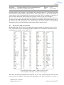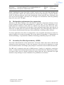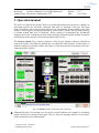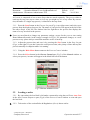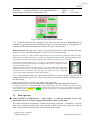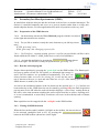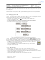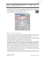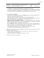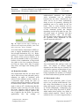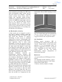
1
Document nr. : EriHeu-20111220-1V01 Document : Operation Manual Veeco IonBeamEtch tool Administrator : Documents Administrator TFF Page nr. : 0 Epcode : E17 Date : 20-12-2011 Author: Eric van den Heuvel Veeco RF350S Ion Beam Etch tool Table of contents 0. 1. 2. Changes compared to previous versions .......................................................................... 1 Safety................................................................................................................................ 2 General information ......................................................................................................... 3 2.1 Equipment................................................................................................................... 3 2.2 Etch recipes (processes).............................................................................................. 3 2.3 Etch rates and selectivities .......................................................................................... 4 2.4 Redeposition and measures for suppression ............................................................... 5 2.5 Secundary Ion Mass Spectrometry (SIMS) ................................................................ 5 3. Operation manual ............................................................................................................. 6 3.1 Process selection and preparation ............................................................................... 7 3.2 Loading a wafer .......................................................................................................... 8 3.3 Run a process .............................................................................................................. 9 3.4 Secundary Ion Mass Spectrometer (SIMS) .............................................................. 12 4. Rules and regulations ..................................................................................................... 16 4.1 Instruction, test and authorization ............................................................................ 16 4.2 Process editor ............................................................................................................ 16 4.3 Tool problems ........................................................................................................... 16 4.4 Wafer handling and penalties ................................................................................... 16 5. Appendix A: Redeposition and Etch mask strategy ....................................................... 18 © Philips Research – MiPlaza/TL Company Restricted Operation manual E17 Document nr. : EriHeu-20111220-1V01 Document : Operation Manual Veeco IonBeamEtch tool Administrator : Documents Administrator TFF Page nr. : 1 Epcode : E17 Date : 20-12-2011 0. Changes compared to previous versions Date Page number 20-12-2012 New version number /01 Description New and combined version of the documents: 1. User Manual Veeco IBE (2006), 2. User Manual Hiden SIMS (2006) and 3. Bedieningsvoorschrift Veeco IBE (RWV011-023-2006) 4. TL-Report 09-001 (E.v.d.Heuvel, 2009) © Philips Research – MiPlaza/TL Company Restricted Operation manual E17 Document nr. : EriHeu-20111220-1V01 Document : Operation Manual Veeco IonBeamEtch tool Administrator : Documents Administrator TFF Page nr. : 2 Epcode : E17 Date : 20-12-2011 1. Safety EMergency Off (EMO)buttons: The tool is equiped with a number of emergency off buttons red yellow that can be pressed in case of potentially dangerous situations. These switches will shut off the electrical power supply to the tool (except for the power supplied to the vacuum pump on the first floor). Additionally, local switches black white are available to shut off the electrical power supplied to the tool AND the local power sockets. Electricity/Radiation/Pinch points: The equipment satisfies all usual safety regulations and there is no danger when the tool is used properly. Danger comes into play when used with removed panels or opened doors (leathal voltages, 1.8MHz RF-radiation, pinch points). Chemical hazardous gases: The only gases in use are argon and (sometimes) oxygen, there are no hazardous gases involved in processing. Maintenance (by qualified people only!!): Once in a while, the process chamber has to be opened in order to remove and clean the liners and the interior of the chamber. Surfaces can be covered with a variety of (etched) materials that may come off as flakes and/or small particles. Proper care must be taken, because materials, especially fine metal particles, may react violently with organic solvents and air and may start a fire by self-ignition. © Philips Research – MiPlaza/TL Company Restricted Operation manual E17 Document nr. : EriHeu-20111220-1V01 Document : Operation Manual Veeco IonBeamEtch tool Administrator : Documents Administrator TFF Page nr. : 3 Epcode : E17 Date : 20-12-2011 2. General information 2.1 Equipment The Veeco RF350S system is a single wafer etch tool equiped with a remote plasma source separated from the process chamber by a set of grids to extract ions from the plasma and create a uniform and collimated ion beam (35cm diameter). In contrast to the local technique of focussed ion beam (FIB) etching, full wafers are exposed to ion bombardment. The etch mechanism is of physical nature and is called ion milling, or ion beam etching (IBE). Virtually every material can be etched with this tool, including the noble metals. Ion energy (in eVolts) and beam intensity (current in milliAmps) can be set independently and the ion energy spectrum is extremely narrow, all in contrast to the situation in traditional sputter etching. The absense of a direct ‘contact’ between plasma and substrates is another difference with sputter etching. Because of low pressure in the process chamber – typically ten times lower than in the plasma source – and consequently long particle mean free path, etched material ends up at the chamber walls or liners, redeposition back from the gas phase is very unlikely to take place. Without measures, charge would build up on the wafer, especially when coated with an insulating layer. This would then lead to beam deflection and potential damage to the wafer due to arcing to grounded surfaces, or arcing within the device layers on the wafer. However, charging and arcing are suppressed by an electron gun, being part of a feedback loop that includes a charge sensor located near the wafer. Software controlled, the gun – called plasma bridge neutralizer (PBN) – prevents build-up of charge. For etch monitoring or endpoint detection, a secondary ion mass spectrometer (SIMS) is available that analyses the secondary ions that get off from the substrate. Intensity changes indicate the passage of interfaces. An option (prepared but not available) is to introduce chemically active gases to assist in the etch process. Depending on the method of introduction, the process is then called reactive ion beam etching (RIBE, introduction of active gases via the plasma source), or chemically assisted ion beam etching (CAIBE, straight introduction of active gas into the process chamber). Both techniques are attractive for dedicated processing only and don’t match well with multipurpose use of the tool. The price to be paid for chemical assistance is fast contamination of source and chamber, frequent preventive maintenance, considerable tool-down time and short life time of the sensitive SIMS detector (if compatible at all with chemical assistance). 2.2 Etch recipes (processes) The set-up of etch recipes – called processes in the Veeco software – is relatively simple. Any combination of three acceleration voltages (200/400/800V) and two beam currents (100/300mA) is available in ready-to-use processes. Almost all of them have argon as the only process gas, only in rare cases oxygen is added for etching with a metal hard mask like Mo (oxydizing the hard mask during the etch). Additional process parameters are the wafer © Philips Research – MiPlaza/TL Company Restricted Operation manual E17 Document nr. : EriHeu-20111220-1V01 Document : Operation Manual Veeco IonBeamEtch tool Administrator : Documents Administrator TFF Page nr. : 4 Epcode : E17 Date : 20-12-2011 tilt angle and the wafer motion. Any tilt angle can be chosen between 0o (wafer fully faces the beam) and 90o (beam parallel to wafer surface, wafer facing UP) or -90o (beam parallel to wafer surface, wafer facing DOWN). In most processes the wafer is rotating at a speed of 10 rpm, for better uniformity and/or better film exposure in case of non-zero tilt angles. In static mode, it is only at 0o tilt angle that the film-to-be-etched is fully exposed to the beam. At non-zero tilt angles unmasked areas can partially be shielded off from the beam, being in the shade of the etch mask profile near structure edges, and wafer rotation is recommended. Nevertheless, for special applications static position can be chosen freely. 2.3 Etch rates and selectivities Rough indications of etch rates for an arbitrarily selected number of materials is given in Table 1. Selectivities can be calculated using these numbers, for example the selectivity for the combination Au and AZ-resist is 45/5.4 ~ 8. Table 1: Typical etch rates (in nm/min) of metals and non-metals at a typical beam setting (400eV, 300mA, 0 degrees tilt), sorted alphabetically (left) and by etch rate (right). Etch rates are linearly proportional to the beam current. The relation between etch rate and beam energy (or voltage) is non-linear and depending on the specific material. As a rule of © Philips Research – MiPlaza/TL Company Restricted Operation manual E17 Document nr. : EriHeu-20111220-1V01 Document : Operation Manual Veeco IonBeamEtch tool Administrator : Documents Administrator TFF Page nr. : 5 Epcode : E17 Date : 20-12-2011 thumb, doubling the energy from 400 to 800eV tends to have less effect than doubling the energy from 200 to 400eV. The relation between etch rate and tilt angle is complex and different for different materials and crystal orientations. Some materials have maximum etch rates at non-zero tilt angles, some have at 0o tilt-angle. For all materials, etch rates gradually drop off to zero at 90o tilt angle. 2.4 Redeposition and measures for suppression Inherent to Ion Beam Etching is the side-effect of materials redeposition. Because of low process chamber pressures and consequently low collision rates, overall redeposition of expelled material is unlikely to take place in a random way from the space above the wafer. More likely is local redeposition on sidewalls of steps and mask edges, those parts that are in direct line of sight when seen from the film-being-etched. Steep and high steps tend to be covered up by expelled material having a finite probability of sticking to those surfaces. For many applications the effects of redeposition is not acceptable and measures need to be taken to suppress it as much as possible. This is the subject of Appendix A: ‘Redeposition in Ion Beam Etching’, a reproduction of MiPlaza Technology Laboratory Report no. 09-001. 2.5 Secundary Ion Mass Spectrometry (SIMS) Part of the etched material is in the ionized state. A fraction of these ions can be collected and analysed by mass spectrometry. In this way progress of an etch can be monitored, as count rates at different masses will change upon passage of an interface between different materials. The IBE tool is equipped with such a SIMS detector. Usually it is applied in stand-alone mode, so without any communication between the tool and the detector. Monitoring at different masses allows users to identify interface(s) during etch runs and to determine the right moment to stop etching or to start countdown of a predefined overetch time. © Philips Research – MiPlaza/TL Company Restricted Operation manual E17 Document nr. : EriHeu-20111220-1V01 Document : Operation Manual Veeco IonBeamEtch tool Administrator : Documents Administrator TFF Page nr. : 6 Epcode : E17 Date : 20-12-2011 3. Operation manual The tool is of single-wafer design. Wafer are loaded and transfered to the process chamber in horizontal position, the ion beam is directed from back- to frontside of the tool. The beam angle of incidence can be chosen freely between 90 (extraordinary: beam parallel to the wafer surface!) and 0 degrees (beam perpendicular to wafer surface). Wafers can be fixed passively or rotated around their axis of symmetry. Wafer cooling is accomplished by mechanical clamping and a flow of helium gas at the wafer backside, helium being the medium to transfer heat from the wafer towards a cooled metal chuck called Fixture. The Control window (Fig.1) shows a planview of the system, together with four subfields to control the system. The planview informs the user about the wafer location, vacuum status of load-lock and process module (PM1) and status of robot arm and the beam shutter (the horizontal green line in PM1). Fig.1: Control window with status bar (bottom) Although the plan view contains several graphical control buttons, for example for switching pumps on/off or for opening/closing gate valves(!), users are urgently asked not to use those, unless stated otherwise in this manual. © Philips Research – MiPlaza/TL Company Restricted Operation manual E17 Document nr. : EriHeu-20111220-1V01 Document : Operation Manual Veeco IonBeamEtch tool Administrator : Documents Administrator TFF Page nr. : 7 Epcode : E17 Date : 20-12-2011 Next, all subfields will be described just the way as they appear when handling and processing wafers. 3.1 Process selection and preparation Additional to the Control window, a recipe editor window is needed for tool operation. It can be accessed via the Main Menu button in the top-left corner (Fig.2). Fig.2: Main Menu button This button enables switching between the Process Control window and the Process Create window (recipe editor), as indicated in the pop-up menu (Fig.3). Fig.3: Main Menu pop-up menu After pressing the Process Create button, the Process Create windows appears (Fig.4). 400V_30deg_10mi n Fig.4: Process Create window © Philips Research – MiPlaza/TL Company Restricted Operation manual E17 Document nr. : EriHeu-20111220-1V01 Document : Operation Manual Veeco IonBeamEtch tool Administrator : Documents Administrator TFF Page nr. : 8 Epcode : E17 Date : 20-12-2011 A Process is composed of one or more Steps that are stored separately. The process editor is used step-by-step, one step at a time, so in a way you might say it is a step editor. By convention, the name of a single-step process, is identical to the step name. 3.1.1 Press the Load button in the Process list part (Fig.4, top-right corner) and select your process from the displayed process list. The name of your process will appear at the left in the line above Step1 in the list. The distinct blue line right above the process line displays the name of a step involved in the process. Users are not allowed to change any parameter settings, except for the process time setting Hours/Minutes/Seconds (in the orange rectangle in Fig.4). For parameter changes, or a new process set-up: please always consult the machine owner or back-up. 3.1.2 Adjust the process time and save it by pressing the Save button in the Step list part (Fig.4, at the right). If you don’t know the exact process time, take plenty of time and stop the process manually on endpoint while it is running. 3.1.3 Using the Main Menu button return to the Process Control window. 3.1.4 Press the Select button in the Process Control part (Fig.5) of the Control window to select your process, its name will appear in the black line below the button. Fig.5: Process Control window 3.2 Loading a wafer 3.2.1 By convention, the load lock is left under vacuum after using the tool. Press Auto Vent in the Auto Vacuum Sequences part (Fig.6) of the Process Control window to vent and open the load lock. 3.2.2 Take notice of the section Rules & Regulations (Sect.4) about wafers. © Philips Research – MiPlaza/TL Company Restricted Operation manual E17 Document nr. : EriHeu-20111220-1V01 Document : Operation Manual Veeco IonBeamEtch tool Administrator : Documents Administrator TFF Page nr. : 9 Epcode : E17 Date : 20-12-2011 Fig.6: Load lock and robot control window 3.2.3 Open the load lock door and place your wafer into the load lock, wafer flat at “12 o’clock”. By gentle rotation feel whether the wafer is fixed in the cutout, it is designed to be compatible with both Semistandard and Jeida wafer flats. Close the door. Wafer detection: the only wafer sensor is present in the load lock. After placement into the load lock, a blue wafer should appear on screen. If so, go to the next step. The sensor is sensitive to wafer backside coatings and in some cases the user has simply bad luck: the coating makes the wafer invisible to the sensor or it leads to an ambiguous perception (wafer displayed blinking present / not-present). Such a situation impeeds any further normal action, however, there is a way around. In case wafer sensing problems, press – by exception – the button Load in the robot control window (Fig.6), the robot will place the wafer in PM1, however, without tool confirmation about wafer presence. Additionally, inform the tool about the presence of a wafer in PM1: after return of the robot arm, move the cursor to the empty position in PM1 where the wafer is supposed to be, double-click at this position and in the pop- up window press Add. A blue disc (=unprocessed wafer) should appear in PM1 on the display. 3.2.4 Check whether the set of 6 lines present in the Process control window (Fig.5) have all changed from black to green. If so, the tool is ready for processing: continue with the steps in the next section. If not all 6 lines in Fig.5 are coloured green, further action is impeeded! If lines other than the 2nd or 6th one remain black, something is wrong: please inform the tool owner. For different reasons, the 6th line, PM online, can be coloured black. It can be changed into green by pressing the only button present in the Process Module 1 part of the Control window (Fig.1). The button in the top-left corner switches between Off line and On Line, the latter being the right one. Although important the button has no additional functionality. 3.3 Run a process Check whether the SIMS detector – when needed – is ready for operation. If not, take preparations (Sect. 3.4) before starting automated processing of the wafer. The etch tool has been designed for automated operation, such that – in principle – the tool takes care of load-lock pump down, wafer transfer to PM1 (robot arm), wafer processing in PM1, wafer transfer back to the load-lock, and load-lock venting. © Philips Research – MiPlaza/TL Company Restricted Operation manual E17 Document nr. : EriHeu-20111220-1V01 Document : Operation Manual Veeco IonBeamEtch tool Administrator : Documents Administrator TFF Page nr. : 10 Epcode : E17 Date : 20-12-2011 Three buttons are available in automated operation (Fig.5): Run to start automated control. This button can be pressed after putting a wafer into the load-lock (normal operation), or after solving the wafer sensing problem and procedures explained at the end of part 3.2.3. Stop to cancel automated control. When pressed during transfer, that action is completed before the tool actually stops. When pressed during processing, the stop command is interpreted as an abort-process command. In all cases, PM1 will go Off line, impeding any further action: it needs to be switched back to On line (see last part of 3.2.4). Auto Unload to get a wafer back from PM1 when automated control has stopped because of a user command. Don’t use this button after a system alarm! 3.3.1 Press the Run button in the Process Control window. (a) In normal situation the load lock will be pumped down in two steps, with a 1 st switch point at 1.0E-1 Torr and a 2nd switch point at 1.0E-4 Torr. (b) The wafer will be transported from the load lock station into the process module PM1. (c) After return of the transport arm and closure of the gate valve, the selected process file will be loaded and the wafer will be clamped mechanically onto the chuck called fixture. (d) Then, helium cooling gas will be supplied to the wafer backside and shortly afterwards the pressure in PM1 is checked. In normal situation there is a temporal pressure rise within tolerance limits and procedures will continue. Too high a pressure indicates excessive escape of helium gas into PM1. In that case, an error message is generated and further processing is stopped automatically. Please consult the tool owner or back-up about how to proceed. The wafer may have been broken or crunched by the clamping mechanism, in any case: don’t try to get it back! (e) If the leakage check has ended successfully, two things will start simultaneously: - fixture tilt, to position the wafer at the tilt angle stored in the selected process, and - ion source ramp up, with the shutter in closed position (*) (*) source ramping is a software controlled procedure, resulting in a beam with the desired acceleration voltage (Beam V) and current (Beam mA), both shown in the Source Readback part of the Control window, Fig.1). (f) Shortly after finishing the previous actions, the shutter (green bar in PM1) will open up: it takes a few seconds before this command takes effect (shutter bar yellow). The shutter is fully open when a ‘shower of ions’ is visualised on screen in PM1. When desired, this is the right moment to manually start the SIMS detector!! © Philips Research – MiPlaza/TL Company Restricted Operation manual E17 Document nr. : EriHeu-20111220-1V01 Document : Operation Manual Veeco IonBeamEtch tool Administrator : Documents Administrator TFF Page nr. : 11 Epcode : E17 Date : 20-12-2011 3.3.2 Elapsed and remaining process time can be found in the Process Module 1 part of the Control window (Fig.1). Without any user action, wafer processing will proceed until the remaining process time has expired. Then, the wafer will be returned automatically to the loadlock and brought back to atmospheric pressure. However, there are two alternative options: 3.3.2a User-defined endpoint (and overetch time) based on SIMS detector signal. Press End Current Step to stop wafer processing (for a single-step process, or stop the current step in a multi-step process). This is the only command in this situation that doesn’t interrupt automated control. The shutter will close and the ion beam will be powered down (remaining process time automatically set to zero). If Abort is pressed, processing will certainly stop, but so will the automated control. PM1 will go Off-line, should be switched back to On line. Wafer can be removed by the command Auto Unload then. 3.3.2b Process interruption. For whatever reason the user may press Stop to interrupt wafer processing. The shutter will close and the ion beam will be powered down, but the remaining process time will not be set to zero. Automated operation will stop as well and the stop command will be interpreted as a process abort. PM1 will go Off-line, should be switched back to On line. Either confirm a process abort by pressing the Abort button, or – more consistent with the very reason to press Stop in the first place – resume processing by pressing the Continue button. Then the ion beam will again be powered up, the shutter opened and processing continued at the point where it was stopped. When finished, press Auto Unload to get the wafer in PM1 back to the load-lock. 3.3.3 Remove the wafer from the load-lock when atmospheric pressure (7.5E+2Torr) has been reached. © Philips Research – MiPlaza/TL Company Restricted Operation manual E17 Document nr. : EriHeu-20111220-1V01 Document : Operation Manual Veeco IonBeamEtch tool Administrator : Documents Administrator TFF 3.4 Page nr. : 12 Epcode : E17 Date : 20-12-2011 Secundary Ion Mass Spectrometer (SIMS) In stand-alone mode the detector and the ion beam etch tool have no mutual interaction. The detector is controlled manually and serves as a process monitor rather than as a fully automated endpoint detector. For most applications this mode of operation works very well. 3.4.1 Preparation of the SIMS-detector 3.4.1a On the desktop activate the Hiden-MASsoft program with the icon shown on the right and maximize the window. 3.4.1b Do you like to monitor exactly the same elements as you did in previous runs? If YES, go to step 3.4.1c. If NO, go to step 3.4.4: Changing a process file. 3.4.1.c By File/Open... open an existing ‘process’ (exp-file) you used before (all files can be found within the file folder C:\SIMS_Stand-alone or one of its subfolders). 3.4.1.d Activate the multiplier by pressing the high voltage up button shown here on the right. The detector is ready for operation now, go to step 3.4.2. 3.4.2 Run the selected program Prepare data acquisition by pressing the 'green light' on the SIMS toolbar. The DataAcquisition pop-up menu will ask for file options, as automated data storage is active and file numbers are up-numbered automatically. The user can choose between either overwrite the existing file, in case the last run is not of interest to the user, or open and store data in a new file. After making your choice the SIMS detector is stand-by for action. As soon as the mechanical shutter in the ion beam tool has opened (Sect. 3.3.1.f) and the ion beam strikes the wafer, SIMS detection can be started by pressing OK in the Data Acquisition pop-up menu. Press OK when the etch tool monitor displays a ‘rain of ions’ coming down on the wafer, at the same moment switching the wafer colour from blue to yellow. Opening earlier is not recommended, as most likely overshoots will occur in the transient state of shutter opening. Data acquisition can be stopped with the ‘red light’ on the SIMS toolbar. 3.4.3 Closing off SIMS detection When the last run has ended (with the 'red light' on the toolbar), the detector has to be de-activated (multiplier back to 0V) by pressing the high voltage down button in the SIMS toolbar (shown here on the right). © Philips Research – MiPlaza/TL Company Restricted Operation manual E17 Document nr. : EriHeu-20111220-1V01 Document : Operation Manual Veeco IonBeamEtch tool Administrator : Documents Administrator TFF Page nr. : 13 Epcode : E17 Date : 20-12-2011 Notice that the high-voltage down button has effect only when an open process file is present in standby phase. After this action close the process file, stop the MASsoft program and switch off the monitor. 3.4.4 Changing a process file 3.4.4.1 The easiest way to make a new process file is to open an existing file with an element selection that come close to the one you are interested in. - first make a copy of the file with a new name ending with the number -00. - change or extend the new file. - the only item that may be changed or extended is the selection of element. - preferable ask the tool owner to carry out this procedure. Fig.6: Listing of monitored elements, e.g. platinum and chromium. 3.4.4.2 Each element you like to monitor is represented by a SEM---Scan x : line (Fig.6). The list should preferentially include all metallic or semiconductor elements present in the materials-to-be-etched, including those present in the material on which the etch should stop. - to add lines, use the mouse to select a line and insert a new line by Edit/Insert new sequence or the toolbar icon (right). - lines may be deleted by mouse selection and the delete key. One exception: the top line cannot be deleted. 3.4.4.3 Mass selection - dubbel-click on a selected line, a Scan editor window will show up (Fig.7). - enter the name of the element you like to monitor (e.g. Si) in the Scan Legend line. - from the table (on paper in the log book) select the mass that corresponds to the selected element, considering the points below Fig.7. *) - enter the mass number in both the Start value and Stop value lines. © Philips Research – MiPlaza/TL Company Restricted Operation manual E17 Document nr. : EriHeu-20111220-1V01 Document : Operation Manual Veeco IonBeamEtch tool Administrator : Documents Administrator TFF Page nr. : 14 Epcode : E17 Date : 20-12-2011 - select the mass channels (Scan lines) you like to monitor (probably all); selection is made with the left-hand mouse button while keeping down the CTRL key on the keybord. - press the binocular icon (right) on the toolbar to open a data view window - be sure you really created a new file name (see 3.4.4.1) - save the file and ignore warnings about possible loss of data Fig.7: Scan Editor window. *) Points of consideration in mass selection: - most elements have more than one mass in the list (natural abundance of isotopes); in principle select the mass that is most abundant (e.g. 208 for Pb) for highest detector count rate (counts/second), but also consider the recommendations given below - count rates are limited to 1e+07 c/s, beyond that value the multiplier will eventually get damaged; the SIMS detector is safeguarded and will ignore the concerning mass channel when exceeding this limit; nevertheless, try to avoid these situations - obviously, NEVER try to monitor the ion beam element (argon) itself! - light elements tend to produce higher counts rates than heavy elements, even when etch rates suggest otherwise (e.g. Al versus Au); this also means that light elements are more likely result in count rates of 1E+7 c/s and beyond, especially when large areas are exposed to the ion beam; in that case take a less abundant mass (e.g. 29 or 30 instead of 28 for Si) - etching is not limited to the wafer, as the ion beam strikes everything in its way inside the process chamber, including stainless steel and titanium parts; elements like Fe, Ni, Cr, Ti, and Mo will always be present in the stream of ions collected by the detector; they will cause a constant background at relatively high count rates and may make it difficult for you to see what it going on in those cases you try to etch down into these very materials when being part of the stack present on the wafer - discrimination between elements of nearly the same mass takes special measures, as mass resolution is limited; e.g. to discriminate between Al (27) and Si (28,29,30), take 26 for Al © Philips Research – MiPlaza/TL Company Restricted Operation manual E17 Document nr. : EriHeu-20111220-1V01 Document : Operation Manual Veeco IonBeamEtch tool Administrator : Documents Administrator TFF - Page nr. : 15 Epcode : E17 Date : 20-12-2011 (no abundance, but still resolution limited Al counts) and 29 or 30 for Si for clarity it is a good habbit to add the monitored mass to the element name, it will appear in the legend discription; additionally use a special mark (like in Si 30!) to point out that the chosen mass doesn’t correspond to the most abundant species of the element 3.4.4.4 Data screen settings - with the IBE tool in idle mode, make a first dummy run by activating the SIMS detectorwith the green light in the toolbar at the top - in the DataAcquisition window select Overwrite current file and press OK - let data acquisition run for a few seconds; virtually no counts will be detected, maybe some low-level noise will show up; by default the y-axis will have linear scale - stop the run with the red light in the toolbar - adjust the settings of the X-axis by clicking the right-handside mouse button somewhere at the periphery of the data plot, select X axis and continue in the subwindow; by default the X-axis has limited history, but you may select otherwise - likewise adjust the settings of the Y-axis; logarithmic scale selection in the full range between 1E+2 and 1E+7 c/s works fine; if too wide, this range can be changed later in the same way, while an etch run and the SIMS detector are in operation - overwriting the first dummy run, do a second dummy run and check the result - save the file and ignore warnings about possible loss of data Sometimes software chooses identical colours for different mass channels, both in the data plot and the legend; in that case: - choose Views/TrendViewSetup and select the element the Available Scan number list - change the data point colour settings - save the file and ignore warnings about possible loss of data The detector is ready now for operation. © Philips Research – MiPlaza/TL Company Restricted Operation manual E17 Document nr. : EriHeu-20111220-1V01 Document : Operation Manual Veeco IonBeamEtch tool Administrator : Documents Administrator TFF Page nr. : 16 Epcode : E17 Date : 20-12-2011 4. Rules and regulations 4.1 Instruction, test and authorization Instructions are given to new users by the machine owner and users are authorized after a successful test. Usually this procedure will do, especially when the authorized persons use the tool regularly. 4.2 Process editor As a rule, users are supposed not to make changes in existing processes, except for the process time. The machine owner has to be consulted when a user likes to make changes, or likes to create a new process. 4.3 Tool problems In case of unusual behaviour of the etch tool or problems, the machine owner / back-up should be informed immediately. Essential for the tool and for all other users: never try to solve problems yourself, limit your contribution to notification of one of the afore mentioned persons, especially when a wafer doesn’t return from the process chamber. 4.4 Wafer handling and penalties The mechanical wafer clamping mechanism imposes restraints on the use and handling of silicon and glass wafers. All users are expected to strictly follow the rules for wafer handling in order to avoid wafer breakage and unnecessary tool down times. - preferably use wafers of standard size (150mm) and thickness (0.67mm) - wafers should have a major flat, both Semistandard and Jeida flat are accepted; confirm good wafer fixture in load lock (flat cut-away at 12 o’clock position) - thin wafers impose an extra risk because of the torques to which they are exposed while being clamped; thin wafers with thickness <0.45mm are not allowed in the tool - bonded wafers and glued sandwiches of wafers are not allowed in the tool - follow the instructions for a 5mm edge exclusion (also along the wafer flat!): this area should be clean, free of resist, tape or any soft or sticky material - the backside of the wafer should be clean as well (no resist, tape or any soft or sticky material) - small substrates should be glued on a carrier wafer (with brown kapton tape only); take notice of the 5mm edge area of the carrier wafer - always consult the machine owner or the back-up in case of doubt Never try to return a wafer from the process chamber to the load-lock after a tool alarm or when the wafer didn’t return in the normal way: usually it worsens the situation! These rules cannot guarantee zero wafer breakage, but at least minimize the risk. © Philips Research – MiPlaza/TL Company Restricted Operation manual E17 Document nr. : EriHeu-20111220-1V01 Document : Operation Manual Veeco IonBeamEtch tool Administrator : Documents Administrator TFF Page nr. : 17 Epcode : E17 Date : 20-12-2011 Penalties If a wafer gets crunched in the tool, it’s up to the tool owner – backed up by technicians – to decide whether that specific wafer or the preparations made by the user are responsible for the accident. If ‘yes’, the user gets a warning first. Prior to the next time this user needs to process in the IBE, the substrate has to be inspected by the IBE tool owner upon compliance with the above mentioned rules. After this, whenever the user is to blame for another ‘accident’, that user permanently loses his authorization to use the IBE tool. If it turns out that a user uses the tool just once in a while, it may become questionable whether this user will keep experienced enough to operate the tool in the proper way. In case of doubt the machine owner may decide to cancel the authorisation. © Philips Research – MiPlaza/TL Company Restricted Operation manual E17 Document nr. : EriHeu-20111220-1V01 Document : Operation Manual Veeco IonBeamEtch tool Administrator : Documents Administrator TFF Page nr. : 18 Epcode : E17 Date : 20-12-2011 5. Appendix A: Redeposition and Etch mask strategy (taken from TL Report 09-001, E. van den Heuvel, 2009: Redeposition in Ion Beam Etching) A1. Introduction In the Veeco RF350S Ion Beam Etching (IBE) system(1) a wide collimated beam of argon ions is applied for etching. It is a physical process, there are no chemically reactive process gasses involved. A very common misunderstanding about IBE is to think that pattern transfer from the mask material to the etched material is absolutely perfect, the etch process is thought to proceed exactly along the line of flight of the incoming ions. A second misunderstanding about IBE is selectivity, which is supposed to be more or less absent, afterall all materials are attacked by ion bombardment. This report pays attention to these two misunderstandings and gives practical suggestions for the selection and treatment of mask materials. A2. Etch rate and selectivity In the Veeco IBE system the ion energy (in eV) and beam current (in mA) can be set independently. Etch rates are proportional to beam current, but the relationship between etch rate (ER) and ion energy is non-linear: ER increases with energy in the low-energy range but more energy has less effect in the high-energy range. Furthermore, ER’s depend on the ion angle of incidence, not just because beam intensity drops by the well-known cosine law as the angle goes from zero (straight-on, normal incidence) to 90 degrees (glancing incidence), but also because of the physics involved. The relationship between ER and angle of incidence depends on the specific material being etched. The ER’s of pure metals and some compounds are shown in Table 1 [shown in Section 2.3 of the operational manual]. These values were taken from literature(2,3), some values were – at random – tested and verified on the Veeco system. A typical ER for gold is 45nm/min (400eV, 300mA, normal incidence). The large variation in ER’s shows that a general remark about IBE lacking selectivity is not applicable, but – admittedly – it depends on specific tasks. Silicon etching with a resist mask has a selectivity of just 1.8 (3.8:2.1), good reason to reject IBE as an appropriate way for standard silicon etching. On the other hand, resist and SiO2 are excellent candidates to etch down into noble metals like Au and Pt, with selectivities of 8 and 4, respectively. A3. Redeposition and etch profile At the impact of energetic ions (Fig. A1, top), their energy is dumped into a small volume close to the substrate surface. Material gets scattered in all directions, according to a material specific distribution (Fig. A1, middle). Inevitably a fraction of material will hit the sidewalls, including the etch mask, with a certain chance to adhere to those walls. IBE is always accompanied by this process of redeposition, a process that prevents clean vertical etching at the edges of structures defined in the mask. Generally the sidewalls are sloped and after resist strip fence-like structures appear at the structure edges (Fig. A1, bottom; Fig. A2). Very often these ‘fences’ are extremely thin and do not always exactly follow the edges, they may partly fall down or disappear, for example during a wet resist strip process. Precautions can be taken to suppress the IBE side-effect of redeposition (Sect. A4-A6). © Philips Research – MiPlaza/TL Company Restricted Operation manual E17 Document nr. : EriHeu-20111220-1V01 Document : Operation Manual Veeco IonBeamEtch tool Administrator : Documents Administrator TFF Page nr. : 19 Epcode : E17 Date : 20-12-2011 unidirectional structures, the in-plane wafer orientation can be alternated between two set values. Alternatively, the wafer can be set to rotate continuously along its axis of symmetry, allowing all unmasked area to be etched by the ion beam. That is, each location will be exposed to the beam for a certain fraction of the rotational period, the fraction depending on the local mask lay-out. The ion beam angle of incidence will then oscillate between + and – the tilt angle. The tilt angle needs tuning for best result, the optimum being dependent on the specific materials involved. Fig. A1: Impact of ions (top), scattering of material and redeposition (middle), final result after resist strip: ‘fences’ (bottom). As a final remark, redeposition in IBE systems is largely dominated by the directline-of-sight mechanism (Fig. A1). Redeposition of species back-scattered within the volume of the process chamber or at the process chamber walls is very unlikely, because of the combination of large mean free paths at the low operation pressures (at least ten times lower than in sputter etch tools) and high wall sticking probabilities. A4. Beam directionality One might think that the ion beam itself can be used to keep clean sidewalls, just by adjusting its angle of incidence with respect to the substrate surface. Indeed, at a particular angle setting the rates of mutual redeposition (bottom to wall & wall to bottom) may balance. However, this tilt o angle is close to 45 , which means that this measure works well only for walls facing the beam. Opposite walls and part of the area to be etched are simply ‘shaded‘ and out of sight for the ion beam. For special applications, like the etching of Fig. A2: Platinum ‘fences’ after resist strip. Just occasionally this strategy works out well, the degree of success largely depends on the mask lay-out. Usually it is very hard to suppress redeposition at every location on the wafer, the ‘shading‘ effect being responsible for troubles, for example at corners and at densely packed structures. A5. Resist mask: reflow From an etch selectivity point of view, resist is an excellent mask material. Usually resist film thickness is in the 1µm range and beyond, in the 50-250nm range in e-beam lithography. Lithography proo files are often steep and close to 80-90 , which makes these profiles very likely to collect etched material. ‘Fences’ like described in Sect. A3 can be suppressed by a © Philips Research – MiPlaza/TL Company Restricted Operation manual E17 Document nr. : EriHeu-20111220-1V01 Document : Operation Manual Veeco IonBeamEtch tool Administrator : Documents Administrator TFF resist treatment preceeding the IBE step. After development many resists can be forced to reflow on a hotplate, such that surface tension forces steep walls to change into smoothly sloped profiles, without loss of pattern definition. For some resists (AZ, HPR) the slope angle can be as o low as ~20 , provided that the specific mask lay-out allows for reflow everywhere. Reflow can be expected to work out well for large structures only, large meaning lateral dimensions of 5 to 10 times larger than the resist thickness. Page nr. : 20 Epcode : E17 Date : 20-12-2011 undesirable effect of IBE facetting at mask edges. A6. Hard mask: selectivity A hard mask can be designed in such a way that it (almost) vanishes within the same amount of time as it takes to fully etch down the material of interest. Advantage of this set-up is optimum suppression of ‘fences‘, disadvantage is the introduction of extra steps in this doublelayer approach. First it takes resist lithography to define the structures, then it takes a wet or dry etch technique to pattern the hard mask, and finally a resist strip preceeding the actual IBE step. In the end the remaining part of the hard mask has to be stripped selectively with respect to all other materials present on the wafer. Practical hardmask material are molybdenum, titanium, tungsten and silicon oxide: they have low etch rates and can easily be patterned by reactive ion etching (RIE). An example of IBE with a hardmask is shown in Fig. A3: a platinum film structured using a Mo hardmask and an argon/oxygen beam. Oxygen was added to oxidize Mo and reduce its etch rate. IBE selectivity dictates the minimum mask thickness needed for the ion beam etch. There are two reasons to take the actual thickness a bit more than that. One is to allow for the possibility of some overetch time, the second is to compensate for the Fig. A3: 10µm wide gaps are opened into a 2.5µm platinum film using an argon / oxygen ion beam and a 0.6µm Mo mask. A6. Conclusion Without proper measures, IBE is accompanied by sloped etch profiles and ‘fences‘. Proper choice of the etch mask material or its pre-treatment helps in effective suppression of fences. In special cases, depending on the mask lay-out, proper choice of the ion beam directionality reduces redeposition of material on sidewalls. References 1. E.van den Heuvel, DTS Report 05-016 (2005). 2. H. Kaufman and R. Robinson, ‘Operation of broad-beam sources’ (1987), data selected from Table XIII-2. 3. Intlvac, website (Ontario, Canada). © Philips Research – MiPlaza/TL Company Restricted Operation manual E17