1
United States Patent 1191
[I ll
4,198,682
Albani et a1.
[45]
Apr. 15, 1980
[54] SYMPTOM COMPRESSION DEVICE
[75] Inventors: Alfonso Albani, Bollate; Ermanno
Maccario, Pregnana Milanese, both
of Italy
[73] Assignee: Honeywell Information Systems
Italia, Milan, Italy
Circuits”, Armstrong, Bell Telephone Laboratories,
May 71.
[21] Appl. No.: 863,463
information including bits signifying symptoms present
[22] Filed:
[30]
Primary Examiner-Gareth D. Shaw
Assistant Examiner—E. Chan
[57]
A symptom compression device receives binary coded
in the course of each operating cycle at selected points
in an integrated logical network, microprocessor or the
Dec. 22, 1977
Foreign Application Priority Data
Dec. 31, 1976 [IT]
like. The device includes a ?rst register, a second shift
Italy ............................. .. 31040 A/76
[51]
Int. Cl.2 .............................................. .. G06F 5/00
[52]
US. Cl.
[58]
Field of Search ..................... .. 235/3021; 328/37;
.. ..... . .....
. . . . ..
364/900; 340/347
register, an EXCLUSIVE OR logic network, and a
display. The binary coded information is received on
parallel inputs of the ?rst register and applied from
DD
parallel outputs of the ?rst register to a set of inputs of
the EXCLUSIVE OR network, a second set of inputs
which is connected to at least some parallel outputs
from the second shift register. A set of outputs from the
307/216; 364/200 MS File, 900 MS File, 200,
900; 340/347 DD
[56]
References Cited
EXCLUSIVE OR network is connected to parallel
inputs of the second shift register. In each cycle, the bits
in the second shift register, which accumulate informa
tion representative of symptoms, are shifted in one di
rection and are recirculated. The display is connected
to the parallel outputs from the second shift register. In
a second embodiment, a third shift register receives the
output from the EXCLUSIVE OR network. A multi
US. PATENT DOCUMENTS
3,024,444
3/1962
Barry et al.
3,370,274
2/1968
Kettley et al.
3,598,979
3,742,459
3/1971
6/1973
Moreau ...... ..
booschen ....... ..
3,771,136
11/1973
Heneghan et al.
364/200
3,772,654
11/1973
Evans et al.
364/200
3,780,277
3,875,344
12/1973
4/1975
Armstrong et a1.
Bogart ............... ..
3,989,894
11/1976
Charnansol
4,021,782
5/1977
328/37
. 364/200
328/37
364/200
.... .. 235/3021
340/347 DD
plexor selectively applies signals from the outputs of the
second or third shift register to the second set of inputs.
The bits in the third shift register, which also accumu
late information as to symptoms, are shifted in the oppo
site direction. A second display is connected to the
364/900
Hoerning ........................... .. 364/900
OTHER PUBLICATIONS
“Machine Aids for Logic Design Veri?cation, Fault
Detection and Fault Isolation", Smith and Chappell,
IEEE Computer Conference, 23 Sep. 71.
“A Deductive Method for Simulating Faults in Logic
L TEST
PLUG
AOWVMS
ABSTRACT
outputs of the third shift register.
7 Claims, 4 Drawing Figures
0,..- 0,
$1 SYNC
1)00
READY
1221 f l £5
21f 6
R1 P
RtA
4
25*\
a1
H
g?)
..
: R13
25
.‘
+
.
17
T-'—°4<—_y
1.7
is
_
30*
R
i
J5
11, ‘5
‘11,
1
DBIN HUM "01-9 J
1 {18
>122
RESET
PREsET
1 34
Z
31
“7E
igq
i
27
2%
1
R2 EXT
:
A I
33)
RZUHBI
'
‘
as
'
‘
In,
v
0'
_
no
,
f
n
59
i
"
COUNTER
['42
1+5
45
CM
DECODER
~
US. Patent
Apr. 15, 1980
Sheet 1 of3
4,198,682
PR‘ORWY ‘ - 7
5’
PORT
5'
PORT
Pnoczs~
()
50R)1 2 ’ TU3
3‘ PROM
)8
h'iliifé’?lm
BUS
Q
R
AM
10
CPU
’
A. BUS
M
> A0 ~~ A15
11
‘
/
i < o. BUS
0
P
Ro
/
CONTROL
c
E
5
> D.
INTE
HLDA
12
> 5m:
WAIT
HOLD
EVENT
3
4,‘
R
('9;
.
$515,“
READY
D1
~4
9
US. Patent
Apr. 15, 1980
Sheet 3 of3
9..
hxuNd
4,198,682
1
4,198,682
2
grams and the monitoring of output signal patterns. The
SYMPTOM COMPRESSION DEVICE
test procedures in present day use can be classi?ed into
four basic categories:
BACKGROUND OF THE INVENTION
The present invention relates in general to new and
improved symptom compression devices and in particu
lar to a symptom compression device for diagnosing
integrated logical networks, microprocessors and the
like.
Large-scale integration circuits such as microproces
sors and similar devices are well known in the art today
and are ?nding wide utilization in digital data handling
systems and apparatus. Problems arise with respect to
the checking of such logical circuits to assure that they
operate correctly. Many of these problems stem from
the complexity and difficulty of carrying out such an
l. Computer simulation: The logical network or mi
croprocessor to be tested is subjected to a diagnos
tice stimulation program. The same program is
performed by a computer which simulates the cir
cuits] behaviour of the logical network and gener
ates output signals.
Unless the output signals from the network and those
from the computer during' the program execution
are equal, a fault is detected.
2. Comparison with a standard sample or “signature
testing": The logical network or microprocessor to
be tested is subjected to a diagnostic stimulation
program. The same program is performed by a
operation, conditioned by the complexity of the circuit
second logical network or microprocessor identi
under test.
cal to the first one, but known to be good, which
Early in the development of the art, computers were
built using discrete components. These components,
consisting of diodes, transistors, capacitors, and resis
tors, were electrically connected into relatively simple
electrical networks to perform elementary logical oper
ations. The further interconnection of such networks
into more complex circuits, including complete elec
tronic data processing systems, enabled the early user to
perform complex logical functions. As a rule, these
discrete components were mounted on printed circuit
boards, each board containing a limited number of com
ponents and a limited number of elementary logic func 30
tion networks.
In the early days of the computer, the distinction
between combinatory and sequential networks was
clear, e.g. between networks where the logical value at
the output terminals is exclusively dependent on the
value of input signals and networks where the logical
value at the output terminals is further dependent on the
history, or on the logical sequence of electrical circuits,
through which the network has passed. For a combina
tory network it is possible to check for correct opera- 40
operates as a standard.
If the ?rst network operates correctly, the output of
the two networks must be identical during program
execution.
3. "Pattern recognition testing” or comparison with a
standard output pattern: The logical network to be
tested is subjected to a diagnostic program and the
output pattern sequence produced is compared
with a standard pattern sequence corresponding to
correct operation and obtained either by logical
means, or by using a network identical to the one
under test but known to be good and subjected to
the same diagnostic program.
4. “Pattern generation" or generation of subsequent
test patterns: The logical network to be tested is
subjected to a diagnostic program which is not
unequivocally defined from the beginning, but
which changes depending on the detected output
pattern.
The stimulating diagnostic program is generated by a
control computer.
A ?fth category can be added which may be de?ned
as “self-diagnosis.” In such a case, the logical network
to be tested is inherently provided with a memory
combination of output signals. Where a number of stim
which stores a diagnostic program, and with circuit
ulations occur independently of each other in a sequen
tial network, it is essential to know the history of the 45 elements within the network which are capable of de
tecting failures of the network when the same is stimu
network in order to check its operation. A diagnostic
lated by the diagnostic program. A limit to the latter
operation thus requires that an ordered sequence of test
tion by assuring that a predetermined combination of
input signals produces a corresponding predetermined
stimulations be applied, starting from a predetermined
status.
Thus, even in the early days of the computer, the
checking of the correct operation of a sequential net
work for possible network faults presented a relatively
dif?cult task. However, the task was simpli?ed by the
fact that discrete components, having accessible termi
nals both at the component level as well as the level of
approach is obviously imposed by the fact that failures
may affect the memory as well as the circuit elements
which are to provide fault detection, thus rendering
impossible or partially impossible the correct execution
of the diagnostic program.
An aspect which must be considered in all of the
above-discussed approaches is their applicability on the
site, i.e. in the place where the network to be tested is
the printed circuit board which then contained rela
installed. Clearly, any test generation which requires
tively simple networks, permitted these difficulties to be
overcome using relatively simple tools. Correct opera
cumbersome equipment difficult to move (as is the case
fully integrated logical networks and microprocessors,
procedures which rely on self-diagnosis performed by
for instance in computer simulation), is excluded from
consideration for all practical purposes. This is particu
tion could be ascertained either by checking the individ
ual components, or by checking the individual net 60 larly so if the test operations can be carried out only in
maintenance centers to which the apparatus to be tested
works on the printed circuit board.
must be transported.
The subsequent use of integrated circuits of greater
Therefore, from a practical point of view, only those
and greater complexity, up to the present utilization of
has brought the di?iculty of such an approach to the 65 the network to be tested itself, or by means of additional
apparatus associated with the network, are of impor
fore and has necessitated the adoption of more sophisti
tance. This means that the fault symptoms must be iden
cated test procedures which require the stimulation of
the entire network input according to diagnostic pro
ti?ed by some element of the network itself, or by
3
4,198,682
4
In accordance with the present invention, the appara
tus comprises a first register for storing the signi?cant
information or symptoms containing patterns which
means of some external apparatus which is easy to
move, such as symptoms dictionaries, correlation tables
among symptoms and faults, and the like.
The self-diagnosis concept, however, does not en
appear at the outputs of the monitored network, or at
any other suitable and accessible point of the network.
A second shift register is connected in cascade to the
tirely solve the problem of on-site fault detection. In
fact, the common basis of test procedures, whatever
they are, requires the execution of a diagnostic program
and hence the control of subsequent output patterns
which occur during execution of the diagnostic pro
first register through interposition of a logical network
which performs a logical operation of EXCLUSIVE
OR between the content of the first register and at least
gram. The detection of an error symptom, for instance 0 part of the content of the second register.
The device operates in such a way that the informa
the discrepancy between an actual output pattern and a
tion contained in the ?rst register at a certain instant, is
correct output pattern corresponding to correct opera
added to the content of the second register by virtue of
tion, even if indicative of a failure is not sufficient, in
the EXCLUSIVE OR operation, so as to alter the infor
general, to identify the failure that occurred. Thus, it is
mation content of the second register. The latter infor
mation contents are then shifted ‘oy one bit position in
necessary to consider a plurality of subsequent symp
toms. The automatic monitoring and evaluation of such
subsequent symptoms, as well as their synthesis, can be
carried out automatically with the aid of a computer.
However, this requires the use of costly and cumber
the second (shift) register. When subsequently new
information is loaded into the first register, this new
information too is added by virtue of an EXCLUSIVE
OR operation to the contents of the second register.
Thus, the information so accumulated in the second
some equipment, which again is moved only with diffi
culty to different test sites. Thus, the utilization of such
a technique is practical only in maintenance and support
register is the result of an EXCLUSIVE OR operation
associated with a shift, performed on each information
centers to which the network to be tested must be
or symptom containing pattern seqneniialiy ioaded into
moved.
25 the first register.
For equipment installed on site, any such monitoring
The device is controlled and timed by suitable con
is carried out by a maintenance operator and is there
trol and timing signals generated by the logical network
fore slow and subject to errors. This is due in part to the
which is under test. The circuitry comprises, in addi
fact that the operation requires the diagnostic program
tion, a counter for counting the accninuiated symptoms
to be halted at each symptom in order to enable the
operator to read and examine it. Subsequently, once the
containing patterns and for stopping the network under
test once a preestablished number of symptoms contain
symptom has been read, the program must be restarted;
ing patterns has been accumulatedv Suitable displays
and ?nally the conceptual synthesis of the several symp
enable the operator to read the contents of the second
toms in a single item of information is required to permit
identi?cation of the fault that occurred.
35
OBJECTS OF THE INVENTION
It is a primary object of the present invention to pro
register, to examine the symptoms contained in the
accumulated pattern and to identify them by compari
son with a fault dictionary showing the nature and loca
tion of the fault.
These and other objects of the present invention to
vide apparatus for monitoring the operation of large
gether with the features and advantages thereof will
scale integrated circuits which is not subject to the 40 appear more clearly from the following description of a
foregoing disadvantages.
preferred form of embodiment when read in connection
It is another object of the present invention to pro
with the accompanying drawings wherein iike refer
vide simple and economical apparatus for diagnosing
ence numerals designate corresponding parts.
the operation of large-scale integrated circuits such as
microprocessors or the like.
45
It is a further object of the present invention to pro
vide symptom compression apparatus which has ade
quate characterizing power to permit the diagnosis of
BRIEF DESCRIPTION OF THE DRAWINGS
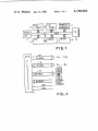
FIG. 1 illustrates a block diagram of a digital data
handling system consisting of microprocessors and
large-scale integrated circuitry.
large-scaie integrated circuits.
FIG. 2 illustrates the logical Sil'itt'ltii‘tf of a “bus’ for
it is still another object of the present invention to 50 transferring information among the ~. era] constituient
elements of the system shown in FIG.
provide apparatus for diagnosing the operation of a
FIG. 3 illustrates a preferred embodiment of a symp
network in which such apparatus is adapted to com
tom compression device for diagnosing logical inte
press a plurality of subsequent network symptoms ap
grated circuit networks such as shown in tilt}. 1.
pearing in subsequent patterns into a single symptoms
FIG. 4 illustrates another emlmrliment of the appara
and is capable of being either incorporated into the
tus shown in FIG. 3.
network under diagnosis, or of existing as an indepen<
dent device.
DETAILED DESCRlP‘l‘l?l‘J till‘ THE
INVENTION
BRIEF DESCRIPTION OF THE INVENTION
In order to understand the features and the operation
The apparatus which is the subject matter of the 60
of the symptom compression device which forms the
present invention may be embodied, for simplicity, as
subject matter of the present invention, it is useful to
integral with the network to be tested, and hence as
summarily describe the structure and the organization
permanent test apparatus. Alternatively, and preferably,
of electronic equipment consisting of in .roprocessors
it may be embodied as an independent device, which is
simpie and inexpensive, readily transported and easily
65
and large-scale integrated circuitry. FIG. 1 shows, by
connected to the network under test whenever it is
way of example, the organizatnini of a central processor,
desired to monitor the operation of the latter and to
detect any fault that may have occurred.
built-up with large-scale integrated circuits, such as
miroprocessors. The central processor may include a
4,198,682
5
or of a limited number of packages, which perform
logic/arithmetic functions as well as control functions
for the whole set of circuits which form the central
processor.
Another integrated circuit unit 2, referred to as TU or
timing unit, provides suitable timing signals for micro
processor 1 as well as for the other circuits.
6
FIG. 2 shows in greater detail the set of wires which
transfer information from and to the microprocessor
CPU. The wires, which are used to establish the con
nection with microprocessor 1, such as the INTEL
8080 microprocessor, form has 8 in FIG. 1.
A first set of wires 10, which holds sixteen wires,
microprocessor 1, consisting of a single circuit package
respectively designated A0, A1, . . . A|5, forms an Ad
' dress Channel or A BUS used by microprocessor l to
forward the address of a memory position or a periph
A third block PROM is identified by reference 3 and
eral unit, in binary coded form, to the other blocks or
units of the system (in particular to memory units and
consists of one or more integrated circuits. Block 3
performs the function of a programmable read only
memory in which microprograms are stored. These
peripheral units).
lead the operation of the system through interpretation
and execution by microprocessor 1.
respectively designated D0 . . . D7, forms a Data Chan
A fourth block RAM is identi?ed by reference num
ber 4 and consists of one or more integrated circuits.
Block 4 performs the function of a read/write memory,
microprocessor 1 to forward to the other units or to
A second set of wires 11, which holds eight wires,
nel or D BUS, having bidirectional properties used by
receive from the other units, binary coded information.
A third set of wires 12, designated “Control & Tim
for storing therein data and programs to be respectively
ing” wires, is used by microprocessor 1 to forward to
handled and executed by the system.
Additional blocks such as 5 and 6, designated l/O 20 other units control and timing signals.
If the Intel 8080A microprocessor is employed for
PORTS, perform interface functions with respect to
microprocessor 1, six of its wires may be used to trans—
external peripheral units such as printers, card reader/
fer the following signals:
INTE (INTERRUPT ENABLE): Depending on its
logical level, this signal indicates whether the micro
punchers, disc units, magnetic tape units, etc. These
blocks too may consist of a single or a limited set of
packages. In case the central processor is provided with 25
processor is in condition to accept or not to accept
a plurality of input/output channels, e.g. a plurality of
external interrupts.
,I/O PORTS, the function of assigning priorities in the
HLDA (HOLD ACKNOWLEDGE): This signal indi
acknowledgement of external interrupt requests is per
cates, depending on its logical level, if the micro
formed by another block 7, which too may consist of a
30
single or a limited set of packages.
The separate blocks communicate with microproces
sor 1 by means of wire set 8, in the form of a channel or
bus. The organization of this channel is considered in
detail below. For the moment, it should be noted that
the channel, or at least part of the wires which form the 35
channel, can be made accessible to external devices by
means of a connector 9, indicated as TC (Test Connec
tor). As such, the logical status at which such wires are
set can be checked.
The structure described is exemplary not only of
central processors constructed of microprocessor mod
ules, but also of central processors built-up of circuits
having a different integration level. When designing
electronic systems and apparatus, the approach fol
lowed is generally to divide the system into functional 45
blocks. These correspond to a plurality of physical
(hardware) blocks interconnected by wires arranged to
form one or, in some cases, a plurality of channels.
processor maintains control over two buses, A BUS
and D BUS, or if such control is transferred to an
other unit. In the latter case, the microprocessor
switches the pins connected to such buses to a high
internal impedance state and allows another unit to
take control over such buses and to apply to such
buses any desired signal con?guration.
SYNC: This is a pulse signal which indicates the begin
ning of a machine cycle.
DBIN (DATA BUS IN): This is a signal which indi
cates to external circuits that the microprocessor is
preset to receive data from outside. It is used to en
able the loading of information placed on DATA
___§US into the microprocessor.
WR (WRITE): This is a signal which indicates to exter
nal circuits that the microprocessor has placed infor
mation on DATA BUS and that such information is
ready to be written into memory or transferred to
other units. The signal may be used as a control signal
to enable a write operation into memory or the load
In the simplest case, each of the blocks shown in FIG.
1 consists of a single integrated circuit of the type which 50 ing of information into input/output interface cir
cuits.
is commercially available, e.g. from INTEL Corpora
WAIT: This is a signal which indicates to external cir
tion under the codes listed in the following table:
cuits that the microprocessor is in a waiting state, e. g.
awaiting the termination of a memory read operation
Code
55
in process.
Block 1:
Central Microprocessor
8080A
Microprocessor 1 (e.g. Intel unit 8080A) further in
Block 2:
Timing Unit
8224
cludes four input pins for connection to four input leads
Block 3:
Read Only Memory
8702A
adapted to receive the following external signals or
8303
Block 4:
Read/W rite Memory
Blocks 5-6:
Interface Unit
Block 7:
Priority and lnterrupt
Management Unit
B3l6A
8l02A-4
81078-4
8212
3255
825!
external events:
8214
RESET: This is a signal which resets the microproces
HOLD: This is a signal forwarded to the microproces
sor which requests the microprocessor to set in its
waiting state and leave control over Address bus and
Data has to an external device, for instance another
microprocessor.
sor to a known initial state.
See Intel 8080—M|'croc0mputer System User’s Manual,
published September 1975.
INT: This is a signal indicative of an interrupt request
sent by an external device.
7
4,198,682
READY: This is a signal which indicates to the micro
processor that information received from memory or
from a peripheral device is available and ready on the
Data bus.
The set of wires, which are used to transfer control
signals and events are designated as Control Bus. Mi
ing or “strobe” signal, either to load the “status
wor " in a suitable status register inside the computer
system, or to load the same status word in a diagnos
tic device external to and connected to the system
through test connector 9.
croprocessor 8080A is further provided with two pins
B. The output from the microprocessor in the form of
binary coded information to be written into memory,
for receiving two cyclical timing signals (pl and 4:2. It
further includes pins (not shown) for connection to
or to be forwarded to a input/output peripheral unit,
is maintained in the Data Bus during two or more
states of a machine cycle following the ?rst state.
suitable power sources at different voltages. The opera
tion of a microprocessor, which is explained in detail in
the aforesaid INTEL manual is similar to that of elec
Speci?cally, the information becomes available after
a certain delay relative to the leading edge of the d);
pulse pertaining to the second state and remains stable
during the whole third state, or during a plurality of
tronic data processing equipment and is performed
through a plurality of “instruction cycles.”
An “instruction cycle" is de?ned as the time required
to interpret and to execute an instruction and comprises
an interpreting phase, or fetching phase, and an execut
states following the second one.
ing phase. An “instruction cycle” comprises one or
more “machine cycles," the latter being de?ned as the
elementary unseverable time units of activity of a com 20
puter.
In the case of a microprocessor, it is preferable to
de?ne a “machine cycle” as the time interval required
by the microprocessor to perform a memory access
operation or access to an input/output channel. For 25
many microprocessors, such as the INTEL 8080A, the
“machine cycle” consists of a plurality of “states.” With
respect to such microprocessors, a “state" is the unit of
unseverable activity of the microprocessor, or the inter
val between two basic timing pulses, for example, two 30
successive (b1 pulses which define the timing period for
It ceases to be signi?cant only following the leading
edge of pulse (b2 pertaining to the state which fol
lows the third state, or the plurality of states dis
cussed above.
The presence of the information during subsequent
states is determined by the logic level of signal
READY at the input to the microprocessor. If this
signal is at logical level 0, which indicates that the
memory or the peripheral unit to which the infor
mation is addressed is not ready to receive the
information, the microprocessor places itself in a
waiting condition for one or more “states" until the
information is accepted.
Another condition for the transfer of the information
requires signal WR, at the output of the micro~
the microprocessor. Pulses 4);; have the same frequency
as pulses dn but are time-shifted relative to (in to provide
within each “state" a suitable intermediate timing sig
nal.
35
As is the case in a computer where different machine
instructions are de?ned, so in a microprocessor different
machine cycles are de?ned in order to perform different
operations such as instruction fetching, memory read/
write, input/output operations, and so on. A number of
processor, be at logical level 1, i.e. that it be pres
ent. Therefore the leading edge of signal READY,
enabled by signal WR through a logical AND
operation, may be used as a loading or "strobe”
signal, either to load the information at the output
from microprocessor into a memory position; to
transfer it to a peripheral unit; or to load it through
test connector 9 into a diagnostic device external to
and connected to the system through the test con
nector 9.
C. When binary coded information is to be read by the
existing microprocessors, including the INTEL 8080A,
characterize and identify each machine cycle by for
warding an 8 bit “status word" on the Data Bus during
the ?rst “state” of each machine cycle. This status word
is accompanied by a timing signal SYNC and is loaded 45
into a suitable register, external to the microprocessor,
using the SYNC signal itself or a SYNC-derived signal
as a strobe signal for loading. The status word can be
used thereafter during the following states, as a source
of suitable control signals.
Such control signals may characterize the address
8
Through an AND operation it may be used as a load
50
placed on the Address Bus as a memory address, a pc
microprocessor, i.e. when it is applied to the input of
the latter, the microprocessor, besides addressing the
memory of the speci?c peripheral unit, generates
signal DBIN. The latter increases with the leading
edge of the ‘in pulse pertaining to the second “state"
of a machine cycle and decreases following a certain
number of “states” only after a READY signal has
been forwarded to the microprocessor to indicate
that the requested information is available to the Data
ripheral unit address, an auxiliary register address, or
Bus. Therefore, the leading edge of signal READY,
simply meaningless information if the machine cycle
enabled by the presence of signal DBIN through a
does not require any data transfer. Further the control 55
signals may de?ne the direction of data transfer. With
out entering here into the details of the timing of the
various signals, which are beyond the scope of the pres
logical AND operation, may be used as a loading or
“strobe” signal either to load the input data into a
ent invention and which can in any event be found in
the above-mentioned catalogue, the following opera
suitable register of the microprocessor, or to load the
data through test connector 9.
D. Data exchange in input to or output from the micro
processor is carried out by means of an addressing
tions are signi?cant:
A. A “status word” is loaded on the Data Bus upon the
operation effected by the microprocessor, by placing
occurrence of the leading edge of timing pulse 4);,
position or the peripheral unit where the data is to be
on the Address Channel the address of the memory
which is received within the ?rst state of each ma
chine cycle. The SYNC signal increases with the
leading edge of pulse (in and decreases with the lead
ing edge of the following :1); pulse. Therefore, pulse
d); is enabled by the presence of signal SYNC.
65
written or from which it is to be read out. Such ad
dress is generated in the ?rst “state" of each machine
cycle, together with the status word, and is main
tained on the address channel for the whole machine
cycle. Thus, it is present when the data to be read or
4,198,682
written, which has been placed on the Data Bus, is
effectively read out or written.
Therefore, even in the latter case the leading edge of
10
address present on the Address Bus and the data present
on the Data Bus, regardless of whether it is input or
system and connected to the latter through test connec
output data.
Section R13 is loaded upon the occurrence of timing
pulse d); which is received through test plug 100 on lead
122 and is applied to an input of logical AND gate 22.
The second input of AND gate 22 receives signal
SYNC, through test plug 100 and lead 23. The output of
tor 9.
AND gate 22 is connected to the timing or strobe input
signal READY, enabled selectively by the presence of
signal WR or DBIN, may be used as a loading or
“stro ” signal to load the address present on the ad
dress channel into diagnostic devices external ,to the
'
From the foregoingv explanation it will be clear that in 0 24 or section R13. Accordingly, as already explained, at
the course of execution of a program which has been
written for diagnostic purposes, the symptoms contain
ing patterns which may be considered at each machine
cycle are as follows:
A. Addresses present on the Address Bus.
B. Data present on the Data Bus, either at the input or
the output of the data processor.
C. “Status word" which de?nes each machine cycle
(whenever the microprocessor is organized to gen
erate such “status word”).
Such patterns may be easily strobed by means of a lim
ited number of timing signals generated by the system
itself, such as for instance those discussed above. Addi
the beginning of each machine cycle the “status wor ”
present on the Data bus is loaded into section R13. This
operation is performed within each machine cycle be
fore the loading of section R1,‘.
15
The outputs of register R|, which number l6+8+8,
are connected to a set of input terminals 25, equal in
number, of a network 110. This network is provided
with a second set of input terminals 26 corresponding in
number to those of the ?rst set. Network 110 performs
a logical EXCLUSIVE 0R operation with respect to
the signal applied to each input of the first set and the
signal applied to a corresponding input of the second
set.
tionally, certain signals present on the control channel
The output set 27 of network 110 has the same num
may be used in the diagnostic device to perform suitable 25 ber of leads as the input set, each lead being connected
control functions.
to a corresponding input of shift register R1.
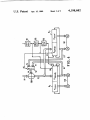
FIG. 3 shows in block diagram form a preferred
Register R; comprises two sections: R2 (A+B) and
embodiment of a diagnostic device in accordance with
R; 5,". Section R; (A+B) has a storage size equal to
the present invention. The diagnostic device is seen to
that of register R1. Section R; EXTis a suitable extension
comprise a plug 100 or TEST PLUG to be connected to
the TEST CONNECTOR of the system to be tested, a
whose storage size can be chosen depending on the
desired degree of symptom compression. As will be
come apparent from the following description, the diag
register R1 to store therein information (or symptoms
containing patterns) read out from the system to be
nostic device compacts a sequence of symptoms con
tested through test connector 9 and test plug 100, a shift
register R2, a logical network 110 for performing an 35 taining patterns, each having a length in bits equal to the
storage size of R1, into a single pattern having a length
EXCLUSIVE OR operation, a set of displays 20 and an
in bits equal to the storage size of R; and containing the
auxiliary element which will be discussed below.
symptoms occurring in the sequence of patterns. In this
Register R] comprises a first section R14, with a stor
sense, a symptom compression into a single pattern is
age size of l6+8 bits, which has its inputs connected to
the pins of test plug 100, corresponding to Address Bus 40 performed.
The greater the storage capacity of R2 EXT, the
A045 and to the Data Bus D04. Register R1 further
smaller is the symptom compression and, obviously, the
includes a second section R13, with a storage size of 8
greater is the cost of the diagnostic equipment. In a
bits which has its inputs connected to the pins of test
practical embodiment of the invention, the preferred
plug 100 corresponding to Data Bus 00.7.
The two sections of register R1 are loaded with infor 45 capacity of R; EXTis equal to that of section R1(A+B).
mation present on their respective inputs upon the oc
currence of two different timing pulses. Section RM is
loaded upon the occurrence of a timing pulse obtained
from the leading edge of signal READY. The latter
signal is received from the system through test plug 100
The outputs 27 of network 110 are connected to parallel
inputs of section R2 (A+B). The parallel inputs of sec
tion R1 mremain unused.
The parallel loading of section R2 (A+B) is per
formed by means of a timing or strobe pulse applied to
on lead 13 and is applied to the input of a univibrator 14.
timing input 28. The corresponding input 29 for parallel
Univibrator 14 is triggered by the leading edge of signal
loading of section R2 EXT remains unused.
The timing pulse for the parallel loading of section
READY and generates a short positive pulse on output
R2 (A+B) is the same as the output from OR gate 20
lead 15. This pulse is applied to one of the two inputs of
AND gates 16 and 17.
55 which is used for the partial loading of register R1.
However, in order to keep in account the propagation
AND gate 16 has its secpld input connected to lead
delay introduced by register R1 and by network 110, it
18 which receives signal WR through test plug 100.
is necessary that this timing pulse be adequately de
AND gate 17 has its second input connected to lead 19
layed. To this end, the output of OR gate 20 is con
which receives signal DBIN through test plug 100.
The output of AND gates 16 and 17 are connected to 60 nected to one input of AND gate 31, whose output is
connected to the input of a delay element 30. The delay
the inputs of an OR gate 20 whose output is connected
element may consist of a delay line or an equivalent
to the timing, or strobe, input 21 of section R1,; of regis
device, such as for instance logical elements connected
ter R1. Therefore a pulse generated by univibrator 14
in series and having an intrinsic propagation delay.
enables the loading of register R14 when one of the two
conditions expressed by the presence of signals WT! or 65 The output of delay element 30 is connected to timing
DBIN is true. This occurs at a time immediately follow
input 28. Register R; in general is arranged to operate as
ing the occurrence of the leading edge of signal
a shift register, for instance as a left shift register. For
this purpose register R; has a shift output 31 and a shift
READY. Accordingly, section R1 ,4 stores in its cells the
11
4,198,682
12
signal can be generated by system elements other than
the microprocessor. When this occurs, the microproces
shift operation.
lntemal to the registers, each memory cell is con
nected in series so that following a shift operation the
contents of each cell of generic order n is shifted into
the cell of order n+ l. The contents of the higher order
cell are transferred out of the register through output 31
and is reintroduced into the lower order cells of the
sor leaves control of the Address Bus and Data Bus to
other apparatus forming part of the system and gener
ates a signal HLDA. Thus, the system has the additional
capability of stopping the operation of the diagnostic
apparatus independently of the zeroing of counter 36.
The HLDA signal is sent through test connector 9
and test plug 100 to the input of inverter 46. The output
of the latter is connected to the second input of AND
gate 31 through wire 47. In this way, when signal
HLDA is high, AND gate 31 is inhibited and any load‘
register through input 32.
In order to assure that the shift operation occurs
when data loaded through the parallel input is stored in
a stable manner, the shift command is obtained by con
necting the output of delay element 30 to the input of a
second delay element 34, and by connecting the output
of element 34 to the clock input 33. The parallel outputs
of shift register R1 are connected to display elements
120, such as for example light emitting diodes, one for
each cell of the register. The on/off status of each such
diode then displays the logical status “1” or “0” of the
information stored in each cell. The parallel outputs of
section R2 (A+B) are connected to the inputs 26 of
logical network 110 which performs a logical EXCLU
SIVE OR operation between the information present
-
As stated above, in the system described the HOLD
input 32 and a shift timing input 33 which controls the
ing or shifting operation of register R2 is prevented.
5
This feature is useful to prevent apparatus of the system
under test, other than the microprocessor, from con
tinuing to activate the diagnostic device by the gem
tion of a READY signal in the presence of WR or
DBlN. It will be understood that this feature is exem
plary only of the broader concept that the operation of
the diagnostic apparatus may be stopped whenever a
pre-established event or condition occurs inside the
system under test.
The diagnostic device which forms the subject matter
of the present invention further includes auxiliary de
vices for the purpose of initializing, presetting, and
The operation of the diagnostic device for providing
symptom compression for diagnostic testing is as fol~
lows. For the sake of simplicity it is assumed that the
length of register R1 is 10 bits and the length of register
stopping the operation of the diagnostic device. A
R2 is 20 bits. The system under test is stimulated by the
RESET push button 35 provides a manual command
for resetting the contents of registers R| and R2 to logi
execution of a diagnostic program. Such a program wiil
on such inputs and that present on inputs 25.
cal level 0 so as to start a diagnostic test procedure
beginning from an initial state which is known. If pre
ferred, the same RESET signal may be provided to the
two registers through plug 100. in such a case, the same
RESET signal is used which is generated internally in
the system under test.
A counter 36 provides a count of the number of ma
chine cycles which have elapsed and hence of the num
ber of loading operations which have been performed
by the diagnostic device. The counter also serves to
stop the operation of the diagnostic device after a pre
determined number of machine cycles have occurred.
To the latter end a set of console keys 37 is provided as
part of the diagnostic device and the outputs 39 of keys
37 are connected to the parallel input of counter 36. A
PRESET button 38 is connected to the present input 40
of counter 36.
By suitable manual setting of the keys and by enabling
the parallel loading of the computer through the activa
tion of PRESET button 38, counter 36 is preset to any
desired state corresponding to a selected number of
cycles, expressed in a binary code. The timing or clock
input 41 of counter 36 is connected to the output of
AND gate 31 so that at each loading control pulse re
ceived by register R2, counter 36 also received a clock
be organized according to suitable criteria, so that de
termined areas of the system will be subjected to some
operation in an ordered and selective manner.
bet it be assumed that in the course of the ?rst ma
chine cycle the information contained in the system
busses is represented by the following binary code:
lst cycle R1 1001011001.
The fourth order bit which is l is underlined to indicate
that it is incorrect and that it must be 0 for a correct
response to the system. Thus, this bit provides an error
symptom, and the 1st cycle code is loaded into register
R1. Register R1, which was reset at the outset, contains
a code configuration of all 0's. The EXCLUSIVE OR
operation performed with respect to the contents of
register R1 and the contents of register R2, bit by bit,
provides the following binary code in register R2 during
the ?rst cycle:
lst cycle R26 (XXIXDOOOOlfDlOllOOl.
The SHIFT operation, performed on the contents of
register R2 in the ?rst cycle, provides the following
binary code in register R2:
is! cycle R1 SHIFT OlXXIOOfIlOlOOlDllOOlO.
pulse.
While in the example under consideration counter 36
It can be seen that the error symptom is now shifted into
is used as a count-down counter, it is well known that
the ?fth order bit position.
electronic counters may be used as count-up or count 60
Let it be assumed now that in the course of the sec
down counters. The outputs of counter 36 are con
ond machine cycle the information contained in the
nected to the inputs of a decoding network 43 which
detects the point when the contents of the counter read
0 and generates a stop command to its output 44. This
code, where once again the fourth order bit, twice un
derlined, is incorrect, i.e. it is 0 rather than 1. Thus,
system busses is represented by the following binary
command is coupled to the system through lead 45, test 65 another error symptom is provided:
plug 100, and test connector 9. It is received on the lead
of the control bus used to transfer the HOLD signal,
thus stopping the operation of the system.
13
4,198,682
14
Information from the output of register R1 is applied
This code is loaded into register R1, while register R1
contains the con?guration discussed above.
The EXCLUSIVE OR operation performed be
tween the contents of the two registers R1 and R1, bit by
bit, loads the following code into register R2 during the
through the leads of set 25 to a ?rst input set of logical
circuit 110, which performs the EXCLUSIVE OR
operation between the information received through
the set of leads 25 and the information received through
a second set of leads 26. The output set 27 of logical
circuit 110 is connected both to the parallel inputs of
second cycle:
section R2 (A+B) of register R2 and to the parallel
inputs of a section R3 (A+B) of register R3. The latter
2nd cycle R29 00000000! 111001200].
The SHIFT operation performed on the contents of
comprises a section R3 (A+B) and an additional section
register R2 in the second cycle provides the following
binary code in register R1:
R3 EXT
The parallel outputs of section R2 (A+B) are con
nected through a set of leads 50 to a ?rst input set 51 of
a multiplexer circuit 52. The parallel outputs of section
2nd cycle R2 SHIFT oooeoooomloiigoow.
15 R3 (A+B) are connected through a set of leads 53 to a
second input set 54 of multiplexer circuit 52. The out
puts of multiplexer 52 are connected to the input 26 of
This code contains as error symptoms two bits, i.e. of
the 5th order and of the 6th order respectively. Thus,
the system has accumulated two error symptoms at this
time.
logical circuit 110.
The above described accumulation operation may
proceed inde?nitely. Any error symptom which is ?
nally located in the 20th order bit position is not lost
The function of multiplexer 52 is to transfer the infor
mation present on inputs 51 and 54 in a mutually exclu
sive way to the outputs connected to inputs 26 of circuit
110. Selection occurs by means of a command signal
however. This is due to the subsequent SHIFI‘ opera
tion, by which such error symptom is reentered in the
0, the information on inputs 51 is transferred to leads 26.
lst order bit position.
There are only two cases by which symptoms may be
lost and both occur for pairs of symptoms:
1. If two symptoms occur in the same bit order but in
different machine cycles (say in different patterns),
the interval in number of cycles between the cycles
in which the two symptoms occur being equal to
the length of register R1 (in bits), then the two
symptoms overlap in the same bit position and thus
cancel each other. In fact, due to the recirculation
applied to an input 55, when this signal is at logical level
25
When the signal is at logical level 1, information on
inputs 54 is transferred to leads 26.
The output of delay element 30, besides being con
nected to the parallel loading input 28 of section R2
(A+B) is further connected to the input of a delay
element 56 whose output is connected to input 55.
The delay of element 56 is chosen so that a pulse
appears on its output when the pulse at its input is al
ready extinguished. Therefore, section Rz (A+B) is
loaded when it receives a command pulse on input 28,
of the content of register R2 for its whole length, 35 with the binary code resulting from the EXCLUSIVE
OR operation performed with respect to the binary
the ?rst symptom, with the occurrence of the cycle
code present on inputs 25 and the binary code on the
in which the second symptom appears, is reentered
output from section R2 (A+B) and present on inputs 26.
in the original position and overlaps with the sec
Immediately thereafter, the delayed command pulse
ond symptom. Further, the EXCLUSIVE OR
generated by delay element 56 selects for transfer the
operation performed on two overlapping symp
toms gives a result which is the same as if the two
symptoms were not present; and, in this sense, the
two symptoms cancel each other.
. If two symptoms occur in different bit order and in
inputs 54 of multiplexer 52. Additionally, the delayed
command pulse is applied through lead 57 to the paral
lel loading input of section R3 (A+B). Thus, section R3
(A+B) receives the latter pulse with the binary code
different machine cycles, the interval in number of 45 resulting from the EXCLUSIVE OR operation per
formed on the binary code present at input 25 and the
cycles between the cycles in which the two symp
binary code on the output of section R3 (A+B).
toms occur being equal to the difference between
The output of delay element 56 is further connected
the order of the second symptom and the order of
to the input of delay element 34, whose output is con
the ?rst symptom, augmented in case of a multiple,
of the length of register R2 in bits, then, once again 50 nected to the shift command inputs of both register R2
and register R3.
the two symptoms overlap in the same bit position
and thus cancel each other for the same reasons
given above.
However, these limitations of the accumulation
Once they have been loaded in parallel with each
other, both registers are subjected to a SHIFT opera
tion. Register R3 is provided with display devices 60
power of the diagnostic device are not such as to ham 55 connected to its outputs. By this arrangement which
subjects the symptoms recorded in the two registers to
per the efficiency of this diagnostic tool. In addition, it
a left shift or right shift respectively, the probability that
is possible by means of simple modi?cations and addi
the two symptoms will cancel each other due to the
tions, to compensate almost completely for the risk of
accumulation process is greatly reduced. In fact, the
symptom loss.
FIG. 4 illustrates another embodiment of the diagnos 60 symptoms which cancel each other in one register will
not, in general, cancel each other in the other register.
tic device according to the present invention. As stated
above, elements common to FIG. 3 and FIG. 4 are
It is apparent then, assuming registers R2 and R3 have
identi?ed by the same reference numbers. Further, all
the same length, that the unique symptoms which may
cancel each other are pairs of symptoms in bits of the
the elements of FIG. 3 which are not shown in FIG. 4
are intended to be part of the embodiment of FIG. 4, 65 same order which occur at a distance, in number of
machine cycles, equal to the length of the two registers,
without any circuit change. The circuit of FIG. 4 uses
expressed in numbers of bits. In case the two registers
two shift registers R2 and R3, as shown, R2 being a
left-shift register and R3 being a right-shift register.
R2, R3 are of different length, the pairs of symptoms
15
4,198,682
16
function of dual selector/multiplexer 4 to 1. In other
words, it consists of a couple of selectors each of
which selects one input over four. It is possible to use
which may cancel each other are determined by differ
ent, readily ascertainable, conditions. In both instances,
the probability that symptoms will be lost is very low.
The embodiment shown in FIG. 4 is exemplary only
such a circuit as a selector of one input over two, as
and modi?cations may be made. For example, rather
required in the case of the exemplary embodiment
than using additional delay elements relative to those
described herein.
considered in FIG. 3, it would be possible to use the
Counter 36: TEXAS INSTRUMENTS integrated cir
same timing system and to perform simultaneously the
cuit SN 54192. By using a suitable number of such
EXCLUSIVE 0R operation by means of two distinct
circuits it is possible to obtain a counting capability
logical circuits, one relative to register R3. The choice l O up to any desired value.
of parameters is determined on a case-by-case basis, by
Decoder 43: This is a circuit which must identify an
economic criteria and eventually by the particular tim
output con?guration of "all zeros.” It may consist of
ing and speed requirements.
a simple NAND circuit having a number of inputs
It will also be clear that rather than using a display for
equal to the number of outputs of counter 36.
each bit of the register R1 and for each bit of register R 3,
TEXAS INSTRUMENTS 8 input NAND gate SN
it is possible to use a limited number of displays together
5430 is suitable for this circuit. By using a plurality
with switching elementswhich connect them alterna
of SN 5430 circuits and connecting their outputs to
tively to the outputs of one or the other of the two
registers, or to a portion of such outputs.
the inputs of an AND gate, a decoder of any de
sired capacity is obtained.
From the foregoing description of the apparatus for 20 It is pointed out once again that the preferred em
the compression and memorization of symptoms in its
bodiments of the present invention shown in FIG. 3 and
block structure, it will be clear that the same can be
FIG. 4 and the circuits inidicated for their implementa
manufactured by using integrated circuits and thus
tion, as well as the set of information which is memo
using a limited number of components. For the sake of
rized as a set of symptoms, are exemplary only. For
completeness of the disclosure, a list of integrated cir 25 example, when the system to be tested fails to make use
cuits using TTL technology is provided, which are
of microprocessors which operate according to multi
capable of performing the logical functions indicated of
ple subsequent “states" within each machine cycle, but
works according to elementary machine cycles, the
Univibrator l4: TEXAS INSTRUMENTS integrated
diagnostic device which forms the subject matter of the
circuit SN54l2l. An additional resistor external to 30
present invention is simplified because there is then no
the integrated circuit is required, whose value deter
need to memorize “status words.” In other cases, it will
mines the duration of the produced pulse.
the various blocks:
be convenient to memorize other kinds of information,
for instance the information present on the control bus.
AND Gates 16, 17, 22, 31: TEXAS INSTRUMENTS
integrated circuit SN 5408. A single package com
prises all four gates.
OR gate 20: TEXAS INSTRUMENTS integrated cir
35
Further, although the diagnostic device has been de
scribed as removably connected to the system to be
tested, it will be clear that it may be integral with the
cuit SN 5432. Only one OR gate, of four provided, is
system to be tested.
used.
From the foregoing discussion it will be clear that
Delay Elements 30, 34, 56: These may consist of a plu
numerous
variations, modi?cations, and changes will
40
rality of diodes, cascade-connected delay lines, or any
now occur to those skilled in the art, all of which fall
other element which has an inherent propagation
within the general scope of the present invention. Ac
delay. For instance, the unused OR gates of TEXAS
cordingly, the invention is intended to be limited only
INSTRUMENTS circuit SN 5432 may be connected
by the appended claims.
in cascade (e.g. with the output connected to the
We claim:
input of another OR gate, one input of each gate 45
1. A symptom compression device for compacting in
being permanently kept at logical level 0).
an
output pattern the symptoms occurring in different
Inverter 46: TEXAS INSTRUMENTS integrated cir
cycles during cyclical operation of a network on binary
cuit SN 5404. Only one of the six inverters on this
chip is used. The remaining inverters, for example,
may be connected in cascade, in pairs, to be used as 50
coded information, comprising:
?rst register means including parallel outputs;
cuit SN 54100 performs the function of an 8 bit
LATCH register, where information is loaded by a
positive clock pulse. Section R“; can be made with 55
three of these circuits. Section R; ,4 can be made with
three of these circuits.
Logical Network 110: TEXAS INSTRUMENTS inte
first loading means for loading at least part of the
binary coded information present in the course of
each operating cycle at selected points of said net
work into said ?rst register means;
second shift register means for storing binary coded
information representative of accumulations of said
symptoms, said shift register means including par
allel outputs;
grated circuit SN 5486. By using eight of such circuits
EXCLUSIVE OR logic means, including a first set
a logical network of 32 logical elements is obtained
which perform the EXCLUSIVE OR operation on
of inputs connected to said parallel outputs of said
32 couples of input signals as required.
Registers R2, R3: TEXAS INSTRUMENTS integrated
nected to at least some of said parallel outputs of
said second shift register means, for effecting an
EXCLUSIVE OR operation, bit by bit, with re
spect to said binary coded information stored in
said first register means and said binary coded in
formation stored in said second shift register
delay elements.
Register R1: TEXAS INSTRUMENTS integrated cir
first register means and a second set of inputs con
circuit SN 54194. By using a suitable number of such
integrated circuits, shift registers of any desired
length can be obtained.
Multiplexer 52: TEXAS INSTRUMENTS integrated
circuit SN 54153. This circuit performs the logical
65
means;
17
4,198,682
means;
timing means operative in each said cycle to control
in sequence the operations of said ?rst loading 5
means, said logic means, said second loading
means, and said second shift register means to pro
vide a one bit shift operation therein; and
display means connected to said parallel output of
(c) EXCLUSIVE OR operation of said logic
means with respect to information contained in
said ?rst register means and at least part of the
(d) a one bit shift operation in one direction of the
information stored in said second register means
and a one bit shift operation in the opposite di
rection of the information stored in said third
register means; and
display means connected to said parallel output of
said second shift register means for displaying the
contents of said second shift register means.
number of cycles have been counted.
5. A symptom compression device for compacting in
an output pattern the symptoms occurring in different
3. A symptom compression device in accordance
with claim 1 and further comprising:
a plug removably adapted for connection of said ?rst
cycles during cyclical operation of a network on binary ’
coded information, comprising:
loading means and said timing means to selected
circuit points of said network.
4. A symptom compression device for compacting in
an output pattern the symptoms occurring in different
cycles during cyclical operation of a network on binary
information contained in said second register
means and loading of the result of said operation
into said second register means,
information contained in said third register
means and storing of the result of said operation
in said third register means, and
said second shift register means for displaying the
contents of said second shift register means.
2. A symptom compression device in accordance
with claim 1 and further comprising:
a cycle counter actuated by said timing means and
having an output; and
means fed by the output of said counter for halting
the operation of said device once a predetermined
,
18
said ?rst register means and at least part of the
second loading means for loading the output from
said logic means into said second shift register
means for receiving a binary coded signal from said
network including bits signifying the symptoms
25
coded information, comprising:
?rst register means including parallel outputs;
?rst loading means for loading at least part of the
binary coded information present in the course of 30
each operating cycle at selected points of said net
work into said ?rst register means;
EXCLUSIVE 0R logic means, including a ?rst set
of inputs connected to said parallel outputs of said
present in the course of each operating cycle at
selected points of said network;
first register means including parallel outputs;
means for loading said binary coded signals into said
?rst register means;
second shift register means for storing binary coded
information representative of accumulation of said
symptoms, said second shift register means includ
ing parallel inputs and parallel outputs;
EXCLUSIVE OR logic means, including a ?rst set
?rst register means and a second set of inputs, and
of inputs connected to said parallel outputs from
parallel outputs;
said ?rst shift register means, a second set of inputs
connected to at least some of said parallel outputs
from said second shift register means, and a set of
outputs connected to at least some of said parallel
second shift register means for storing binary coded
information representative of accumulations of said
symptoms, said second shift register means includ
ing parallel inputs, at least some of said parallel
inputs of said second shift register means;
timing means operative in each said cycle to control
inputs being connected to the parallel outputs of
said logic means, and parallel outputs;
third shift register means including parallel inputs, at
in sequence the operations of said means for load
ing said binary coded signals into said ?rst register
least some of said parallel inputs of said third shift
register being connected to the output of said logic 45
means, and parallel outputs, the shift direction of
said third register means being opposite to that of
said second shift register means;
a selector circuit having ?rst parallel inputs con
nected to at least some of the parallel outputs of
said second shift register means, second parallel
inputs connected to at least some of the parallel
outputs of said third shift register means and paral
lel output said selector circuit being adapted to
apply on said parallel outputs of said selector cir
cuit to said second set of inputs of said logic means,
means, said logic means, loading said second shift
register means from said logic means, and shifting
the bits stored in said second shift register means in
one direction; and
output means connected to said parallel outputs of
said second shift register means for receiving the
contents of said second shift register means.
6. A symptom compression device in accordance
with claim 5, further comprising means for recirculating
said bits stored in said second shift register means.
7. A symptom compression device in accordance
with claim 5, further comprising third shift register
means having at least some inputs connected to said set
of outputs, multiplexor means for selectively applying
signals from said parallel outputs of said second shift
in a mutually exclusive way, the information con
tained in at least part of said second or said third
register means or from parallel outputs of said third shift
register means;
timing means operative in each cycle to control in 60 register means to said second set of inputs, and second
control means for shifting the bits stored in said third
sequence the operations of:
shift register means in a direction opposite to said one
(a) loading of said ?rst register means,
direction.
(b) EXCLUSIVE OR operation of said logic
a
means with respect to information contained in
65
s
a
a
e