1
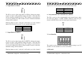
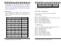
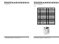
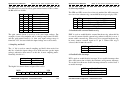
Operations Manual
PCI 12 bit data acquisition card
Operations Manual
CHAPTER 1
•
INTRODUCTION
•
•
•
The PCI bus 12 bit data acquisition card is a 32 bits PCI bus adapter
with Plug and Play (PnP) features, it is a programmable I/O
interface for Pentium or compatible computers. The PnP features let
hardware configuration for IRQ and I/O address is detected by
BIOS automatically, you don’t need set switch and jumper.
PCI 12 bit data acquisition card
Provides software, external hardware signal or internal
counter to trig A/D conversion.
By using sampling and hold to get A/D signals.
Interrupt or polling driven selectable.
Gain control factor selectable from 1 to 8.
The PCI bus 12 bit data acquisition card is a high precision data
conversion/acquisition system. It contains 16 analog to digital
channels with unipolar or bipolar input, 2 digital to analog channels
with unipolar or bipolar output and 1 digital I/O channel with 16 bit
line. The on board 8254(71054) chip provides programmable
interval timer/counter functions to trig A/D conversion. The PCI bus
12 bit data acquisition card also provides interrupt driven for
convention A/D input.
The features of the PCI bus 12 bit data acquisition adapter
are:
•
•
•
•
•
•
•
•
32 bits PCI bus with Plug and Play (PnP) features.
Programmable I/O control functions.
Provides 16 A/D channels and the resolution is 12 bits.
Provides 2 D/A channels and the resolution is 12 bits.
Unipolar or bipolar selectable.
Input voltage range from 0 to 10V or 0 to 20V for unipolar,
and from –5V to 5V or –10V to 10V for bipolar.
Provides 1 digital input/digital output channels and the
resolution is 16 bits.
Provides three 16 bits counter to trig A/D conversion.
DECISION Computer International
1
2
DECISION Computer International
Operations Manual
PCI 12 bit data acquisition card
Operations Manual
PCI 12 bit data acquisition card
CHAPTER 2
CHAPTER 3
UNPACKING INFORMATION
SYSTEM REQUIREMENTS
Check that your PCI bus 12 bit data acquisition package
includes the following items:
Before installing your PCI bus 12 bit data acquisition
adapter, make sure that:
•
•
•
•
PCI bus 12 bit data acquisition adapter.
User manual.
Software utilities.
Warranty form.
DECISION Computer International
•
•
3
4
The host computer is an Pentium compatibles.
The seven jumpers' blocks are correctly configured to
coincide with the operating system you are using.
DECISION Computer International
Operations Manual
PCI 12 bit data acquisition card
Operations Manual
PCI 12 bit data acquisition card
CHAPTER 5
CHAPTER 4
HARDWARE CONFIGURATION
HARDWARE INSTALLATION
Your PCI bus 12 bit data acquisition adapter is designed to be
inserted in any available slot in your Pentium or compatibles. In
order to gain access to the expansion slots, follow the steps listed
below:
5.1 Introduction
The seven jumper blocks on the PCI bus 12 bit data acquisition
adapter must be configured correctly in accordance with the
operating system you are using.
1. Turn off all power to your computer and all peripheral
devices before installing your 12 bit data acquisition adapter.
2. Remove the cover of the computer.
3. Insert the pre-configured 12 bit data acquisition adapter into
any available slot. Make sure the adapter is firmly seated in
the chosen slot.
4. Replace the cover of the computer.
JP1 (Jumper 1)
Determines AD526 (gain control factor) is used.
JP2 (Jumper 2)
Determines to adjust LF398 input voltage offset.
JP3 (Jumper 3)
Determines to adjust SPT574( ADS574JP )input voltage offset.
Note:
1. You must adjust the A/D full scalar reference voltage by
screwing the VR resistor. (see VR Full Scalar Adjustment).
2. You must setup everything including the connection of the
signal input/output into the DB25 and J2 connectors before
turning on the PC power, otherwise it may damage the card.
JP4 (Jumper 4)
Determines A/D and voltage range.
JP5 (Jumper 5)
Determines unipolar or bipolar for A/D channel.
JP6 (Jumper 6)
Determines unipolar or bipolar for D/A channel 1.
JP7 (Jumper 7)
Determines unipolar or bipolar for D/A channel 2.
SW1 (Switch 1)
Identifies card number.
DECISION Computer International
5
6
DECISION Computer International
Operations Manual
PCI 12 bit data acquisition card
Operations Manual
PCI 12 bit data acquisition card
5.2 Configuration for Jumper
It is important to refer to the user manual to determine the correct
configuration. Please contact your supplier if you have any
difficulties with configuration.
Please refer to the following settings for each jumper block.
DECISION Computer International
7
8
DECISION Computer International
Operations Manual
PCI 12 bit data acquisition card
1. I/O Port Address
The plug and play features set I/O port address automatically, please
refer the device manager of control panel to get base port address
of this adapter.
2. Voltage Range
JP4 is used to select a range of A/D voltage from 0 to 10 volts or to
a maximum voltage of 20 volts. Shorting pin 1 and pin 2 will have
a voltage range of 10 volts, while shorting pin 2 and pin 3 will have
a voltage range of 20 volts.
JP4
Jumper
short 1, 2
short 2, 3
Voltage Range
10 Volts
20 Volts
3. Unipolar or bipolar
JP5
Operations Manual
PCI 12 bit data acquisition card
unipolar or bipolar of D/A channel 1, and JP7 is used to select
unipolar of bipolar of D/A channel 2. For JP5, shorting pin 1 and
pin 2 selects bipolar setting, while shorting pin 2 and pin 3 selects a
unipolar setting. For JP6 and JP7, shorting pin 1 and pin 2 selects
bipolar setting, while shorting pin 3 and pin 4 selects a unipolar
setting.
Jumper
JP5
JP6, JP7
short 2, 3
short 3, 4
short 1, 2
short 1, 2
Polarity
unipolar
bipolar
The combination of voltage range and polarity are shown in the
following:
JP4
JP5
Voltage Range
Short 1,2
Short 1,2
-5V to 5V
Short 1,2
Short 2,3
0V to 10V
Short 2,3
Short 1,2
-10V to 10V
Short 2,3
Short 2,3
0V to 20V
JP6, JP7
JP6,7
Voltage Range
Short 3,4
0V to 10V
Short 1,2
-10V to 10V
Selects unipolar/bipolar of A/D or D/A channels. JP5 is used to
select unipolar or bipolar of A/D channel, JP6 is used to select
DECISION Computer International
9
10 DECISION Computer International
Operations Manual
PCI 12 bit data acquisition card
Operations Manual
PCI 12 bit data acquisition card
inputs to be read and converted. It is the normal input mode.
4. Input Mode for LF398
JP2
Jumper
short 2, 3
short 1, 2
The JP2 is used to adjust input offset of LF398. Setting the jumper
to pin 2 and pin 3 will ground the input value (0V), so the data that
will be converted should also be 0. This setting is used whenever
we need to calibrate the VR1 variable resistors so that the minimum
voltage will be attained.
6. Programmable Gain Control Factor (AD526)
The JP1 is used to select programmable gain control factor, when
not short the jumper, it enable AD526, otherwise short the pin
means no AD526 work (can not control gain control factor).
Shorting jumper to pin 1 and pin 2 will make use of the channel
inputs to be read and converted. It is the normal input mode.
Jumper
short 2, 3
short 1, 2
Input Mode
Ground
Normal Input
JP1
Input Mode
Ground
Normal Input
Jumper
short
open
AD526
no AD526
AD526
5. Input Mode for SPT574
7. Card Identifier
JP3
The JP3 is used to adjust input offset of SPT574. Setting the jumper
to pin 2 and pin 3 will ground the input value (0V), so the data that
will be converted should also be 0. This setting is used whenever
we need to calibrate the VR2 or VR4 variable resistors so that the
minimum voltage will be attained.
The switch is used to identify card number, default setting is card 15,
and there are two methods to set the card number:
Shorting jumper to pin 1 and pin 2 will make use of the channel
a. PnP mode
DECISION Computer International
11
12 DECISION Computer International
Operations Manual
PCI 12 bit data acquisition card
Just plug in PCI bus 12 bit data acquistion adapter into PCI slot,
the PCI BIOS will allocate I/O address to each adapter
automatically and assign card number start from 0 to each adapter.
You may set any card number at PnP mode, and you need use
software tools to distinguish port id. Almost all of the operating
systems run at PnP mode..
b. manual mode
Set card number by card identifier switch, the PCI BIOS will
assign pre-allocated I/O address to each adapter. Please set
different card number to each adapter (do not duplicate card
number setting).
1
2
3
4
OFF
OFF
OFF
OFF
Card Number
15
ON
OFF
OFF
OFF
14
OFF
ON
OFF
OFF
13
ON
ON
OFF
OFF
12
OFF
OFF
ON
OFF
11
ON
OFF
ON
OFF
10
OFF
ON
ON
OFF
9
ON
ON
ON
OFF
8
OFF
OFF
OFF
ON
7
ON
OFF
OFF
ON
6
OFF
ON
OFF
ON
5
ON
ON
OFF
ON
4
OFF
OFF
ON
ON
3
ON
OFF
ON
ON
2
DECISION Computer International
Operations Manual
PCI 12 bit data acquisition card
OFF
ON
ON
ON
1
ON
ON
ON
ON
0
The card number starts from 0 to 15.
5.3 I/O Address Specification
The I/O address specification are shown in the following:
For READ input
port + 0:
port + 2:
port + 6:
port + 8:
port + 9:
port + A:
port + B:
input 12 bit A/D data.
clear the interrupt signal that generated from the adapter.
16 bit digital signal input.
counter 0 I/O buffer (8254 IC).
counter 1 I/O buffer (8254 IC).
counter 2 I/O buffer (8254 IC).
counter control register (8254 IC).
For WRITE output
port + 0: select A/D channel number, enable/disable the selected
channel, select IRQ and select control method.
port + 2: 12 bit D/A channel 1.
port + 4: 12 bit D/A channel 2.
port + 6: 16 bit digital output.
port + 8: counter 0 I/O buffer (8254 IC).
port + 9: counter 1 I/O buffer (8254 IC).
port + A: counter 2 I/O buffer (8254 IC).
port + B: counter control register (8254 IC).
13
14 DECISION Computer International
Operations Manual
PCI 12 bit data acquisition card
Operations Manual
PCI 12 bit data acquisition card
5.4 VR Full Scalar Adjustment
2. A/D Calibration
VR Number
VR1
VR2
VR3
VR4
VR5
VR6
Function
Offset voltage of LF398
A/D bipolar offset voltage
SPT574 reference voltage
SPT574 reference voltage
D/A channel 1
D/A channel 2
Before adjust your AD/DA voltage offset, please run
PCIADV03.EXE program under MS/DOS, then select calibration
function as follows.
1. D/A Calibration
VR5 is used to adjust the D/A channel 1 offset voltage, and VR6 is
used to adjust the D/A channel 2 offset voltage.
To adjust D/A channel 1 offset voltage, please follow the step
shown in the below:
Step 1: short pin 1 and pin 2 of JP6, then adjust VR5 to let J1-15
output range from –10V to 10V.
Step 2: short pin 3 and pin 4 of JP6, then adjust VR5 to let J1-15
output range from 0V to 10V.
To adjust D/A channel 2 offset voltage, please follow the step
shown in the below:
Step 1: short pin 1 and pin 2 of JP7, then adjust VR6 to let J1-03
output range from –10V to 10V.
Step 2: short pin 3 and pin 4 of JP7, then adjust VR6 to let J1-03
output range from 0V to 10V.
DECISION Computer International
15
Step 1: short pin 2 and pin 3 of JP2, pin 2 and pin 3 of JP3, pin 1
and pin 2 of JP4, and pin 1 and pin 2 of JP5, then adjust VR3 to let
the output value is 2047.
Step 2: short pin 2 and pin 3 of JP2, pin 2 and pin 3 of JP3, pin 1
and pin 2 of JP4, pin 2 and pin 3 of JP5, then adjust VR2 to let the
output value is 0.
Step 3: short pin 2 and pin 3 of JP2, pin 1 and pin 2 of JP3, pin 1
and pin 2 of JP4, and pin 1 and pin 2 of JP5, then adjust VR1 to let
the output value is 2047.
Step 4: short pin 1 and pin 2 of JP2, pin 1 and pin 2 of JP3, pin 1
and pin 2 of JP4, and pin 2 and pin 3 of JP5, then input voltage from
each A/D channel to check whether input voltage is equal to output
voltage. In this step, please adjust VR4. The A/D channel is defined
from J1-4 to J1-11 and J1-16 to J1-23.
You may repeat Step 1 to Step 4 if necessary.
5.5 Diagnostic Test
The PCIADV03.EXE also provides some diagnostic test functions:
1. DIO loopback test
2. DIO output test
3. DIO input test
4. A/D and D/A loopback test
Please short pint 1 and pin 2 of JP5, pin 2 and pin 3 of JP4, pin 1
and pin 2 of P3, pin 1 and pin 2 of JP2, and pin 1 and pin 2 of JP1,
also short D/A channel (J1-15) to A/D input channel, then check
whether the error value is less than 20.
5. D/A output test
16 DECISION Computer International
Operations Manual
PCI 12 bit data acquisition card
6. A/D input test
Operations Manual
PCI 12 bit data acquisition card
5.6 Pin Assignments
1. J1
Pin
1
2
3
4
5
6
7
8
9
10
11
12
13
DECISION Computer International
17
Function
+ 12 V
/EXTRG
D/A channel 2
CH14
CH12
CH10
CH8
CH6
CH4
CH2
CH0
GND
+5 V
Pin
14
15
16
17
18
19
20
21
22
23
24
25
Function
-12 V
D/A channel 1
CH15
CH13
CH11
CH9
CH7
CH5
CH3
CH1
GND
18 DECISION Computer International
Operations Manual
PCI 12 bit data acquisition card
Operations Manual
PCI 12 bit data acquisition card
CHAPTER 6
2. J2
I/O PORT CONTROL
Pin
Function
1
Function
Pin
14
D1
6.1 Input Port
2
GND
15
D2
1. port + 0
3
+12 V
16
D3
4
GND
17
D4
MSB
0 0
5
D8
18
D5
6
D9
19
D6
2. port + 2
7
D10
20
D7
8
D11
21
When read this port means clear the interrupt signal that generated
from the adapter.
9
D12
22
10
D13
23
0
0 11 10 9
8
7
6
5
4
3
2
LSB
1 0
Input A/D data, only D0 to D11 are useable, the highest nibble are 0.
3. port + 6
MSB
15 14 13 12 11 10 9
+5 V
11
D14
24
GND
12
D15
25
-12 V
13
D0
26
GND
7
6
5
4
3
2
LSB
1 0
Digital input channel. Before read this port, you must write FF value
to this port.
4. port + 8
Counter 0 I/O buffer (8254 IC).
1
. . . . . . . . . . . . .
. . . . . . . . . . . . .
2
DECISION Computer International
8
5. port + 9
Counter 1 I/O buffer (8254 IC).
19
20 DECISION Computer International
Operations Manual
PCI 12 bit data acquisition card
Operations Manual
PCI 12 bit data acquisition card
6. port + A
6.2 Output Port+0
Counter 2 I/O buffer (8254 IC).
The output port address+0 is used to control A/D conversion. The
low 8 bit control format is :
7. port + B
MSB
x
R2
Counter control register (8254 IC).
R1
R0
C3
C2
C1
LSB
C0
1. Select A/D channel number
The C0 to C3 are used to select input channel number.
C3
0
0
0
0
0
0
0
0
1
1
1
1
1
1
1
1
C2
0
0
0
0
1
1
1
1
0
0
0
0
1
1
1
1
C1
0
0
1
1
0
0
1
1
0
0
1
1
0
0
1
1
C0
0
1
0
1
0
1
0
1
0
1
0
1
0
1
0
1
Input Channel
CH0
CH1
CH2
CH3
CH4
CH5
CH6
CH7
CH8
CH9
CH10
CH11
CH12
CH13
CH14
CH15
2. Select gain control factor
DECISION Computer International
21
22 DECISION Computer International
Operations Manual
PCI 12 bit data acquisition card
The R0 to R2 are used to select gain control factor, if JP1 is short,
the R0 to R2 are disable.
R2
0
0
0
0
1
1
1
1
R1
0
0
1
1
0
0
1
1
R0
0
1
0
1
0
1
0
1
Operations Manual
PCI 12 bit data acquisition card
4. Select trig method
The SE0 and SE1 are used to select trig method for A/D converter,
user can select software trig, external hardware trig or trig by 8254.
Gain Control Factor
*1
*2
*3
*4
*5
*6
*7
*8
SE1 SE0
0
0
0
1
1
0
1
1
Selection
Software trigger by TRI bit
Software trigger by TRI bit
External trig from J1-2
Trig by 8254
5. Enable/disable external hardware trig
The gain control factor is used to scale your input voltage. For
example, if you select unipolar and its voltage range from 0 to 20V,
and the gain control factor is *8, then your input voltage range is
from 0 to 2.5V, because whole the input voltage was scale 8 times.
ENX is used to enable/disable external hardware trig, when this bit
is set to 0, it means disable external trig, otherwise this bit is set to 1
means enable external trig. When user select external hardware trig,
he must connect external signal to J1 pin 2. When 8254 trig is
selected, this bit must be set to 1.
3. Sampling and hold
The “x” bit is used to control sampling and hold, when write 0 to
this bit, it latch the input voltage to let A/D converter get the input
voltage, otherwise when write 1 to this bit, it enter sampling mode.
Normally, this bit is 1.
x bit value
0
1
ENX
0
1
Enable/Disable
Disable external trig
Enable external trig
6. Enable/disable interrupt
INT is used to enable/disable interrupt. If user enable interrupt, then
after A/D conversion is finish, the hardware will generate interrupt.
To set this bit to 0 means disable interrupt, otherwise set this bit to 1
to enable interrupt.
Action
Hold
Sampling
The high 8 bit control format of port address+0 is:
MSB
X
X
X
INT
0
1
LSB
TRI INT ENX SE1 SE0
DECISION Computer International
23
Enable/Disable
Disable interrupt
Enable interrupt
24 DECISION Computer International
Operations Manual
PCI 12 bit data acquisition card
Operations Manual
PCI 12 bit data acquisition card
7. Start software trig
The 12 bit D/A output channel 2.
TRI is used to start software trig. Normally, this bit is 0, when user
start software trig, he must set this bit to 1, to let A/D converter start
to convert. This software trig is enable while the signal from 0 to 1.
3. port + 6
MSB
15 14 13 12 11 10 9
TRI
0
1
Enable/Disable
Normal
Start software trig
8
7
6
5
Digital output channel.
4. port + 8
counter 0 I/O buffer (8254 IC).
8. Start 8254 trig
When user select trig by 8254 (SE1=1 and SE0 =1), he must enable
the gate by set ENX bit. The clock rate of 8254 is 1M, it is
connected to counter 0, then the output of counter 0 is connected to
counter 1, so that user need divide the clock by counter 0 then
divide it by counter 1. The divided clock rate of counter 1 is used to
trig A/D conversion.
5. port + 9
counter 1 I/O buffer (8254 IC).
6. port + A
counter 2 I/O buffer (8254 IC).
7. port + B
counter control register (8254 IC).
6.3 Data Output Port
1. port + 2
MSB
0 0
0
0 11 10 9
8
7
6
5
4
3
2
LSB
1 0
7
6
5
4
3
2
LSB
1 0
The 12 bit D/A output channel 1.
2. port + 4
MSB
0 0
0
0 11 10 9
8
DECISION Computer International
25
26 DECISION Computer International
4
3
2
LSB
1 0
Operations Manual
PCI 12 bit data acquisition card
Operations Manual
1
1
1
1
1
1
CHAPTER 7
PROGRAMMING EXAMPLES
To use A/D converter, user must following the steps:
Step 1: Select A/D channel number.
Step 2: Hold the input signal.
Step 3: Start A/D conversion.
Step 4: Get results.
PCI 12 bit data acquisition card
0
0
1
1
1
1
1
1
0
0
1
1
0
1
0
1
0
1
CH10
CH11
CH12
CH13
CH14
CH15
7.2 Hold the Input Signal
Set x bit of port address+0 (low 8 bits) to 0 to latch input signal.
In the following we will describe each step:
MSB
x
7.1 Select A/D Channel Number
Set C3 to C0 of port address+0 (low 8 bits) to select A/D channel
number.
MSB
C3
C3
0
0
0
0
0
0
0
0
1
1
C2
0
0
0
0
1
1
1
1
0
0
C1
0
0
1
1
0
0
1
1
0
0
C0
0
1
0
1
0
1
0
1
0
1
C2
C1
7.3 Start A/D Conversion
Set SE0 and SE1 of port address+0 (high 8 bits) to select trig
method for A/D converter.
LSB
C0
MSB
X
X
Input Channel
CH0
CH1
CH2
CH3
CH4
CH5
CH6
CH7
CH8
CH9
DECISION Computer International
LSB
SE1 SE0
0
0
0
1
1
0
1
1
LSB
TRI INT ENX SE1 SE0
X
Selection
Software trigger by TRI bit
Software trigger by TRI bit
External trig from J1-2
Trig by 8254
1. By using software trigger
1.1 Set or reset INT bit to enable/disable interrupt.
27
28 DECISION Computer International
Operations Manual
INT
0
1
PCI 12 bit data acquisition card
Enable/Disable
Disable interrupt
Enable interrupt
Operations Manual
PCI 12 bit data acquisition card
2.1 Write an interrupt service routine.
2.2 After conversion, the adapter will generate an interrupt to start
the interrupt service routine.
2.3 The interrupt service routine read 12 bits result from port
address + 0.
1.2 Write 0 to TRI bit to start conversion.
2. By using 8254 trigger
MSB
0 0
2.1 Set or reset INT bit to enable/disable interrupt.
2.2 Set the ENX bit to 1.
2.3 Start 8254 counter.
The clock rate of 8254 is 1M, it is connected to counter 0, then the
output of counter 0 is connected to counter 1, so that user need
divide the clock by counter 0 then divide it by counter 1. The
divided clock rate of counter 1 is used to trig A/D conversion
0
0 11 10 9
8
7
6
5
4
3
2
LSB
1 0
2.4 The interrupt service routine read port address + 2 to clear
interrupt signal.
7.5 How to Use D/A Converter
1. Write 12 bits D/A to port address + 2 (D/A channel 1).
3. By using external trigger
MSB
0 0
3.1 Set or reset INT bit to enable/disable interrupt.
3.2 Set the ENX bit to 1.
3.3 Send “1” to “0” pulse from J1-02 pin.
0
0 11 10 9
8
7
6
5
4
3
2
LSB
1 0
2
LSB
1 0
2. Write 12 bits D/A to port address + 4 (D/A channel 2).
MSB
0 0
7.4 Get Results
0
0 11 10 9
8
7
6
5
4
3
There are two methods to get the results of A/D conversion.
3. After 30us, the D/A converter will finish output procedure.
1. By using polling
7.6 How to Use Digital Output Channel
After start conversion, wait about 50us to get the conversion result.
Write data to port address + 6.
2. By using interrupt
DECISION Computer International
29
30 DECISION Computer International
Operations Manual
MSB
15 14 13 12 11 10 9
PCI 12 bit data acquisition card
8
7
6
5
4
3
2
LSB
1 0
Operations Manual
PCI 12 bit data acquisition card
APPENDIX A
WARRANTY INFORMATION
7.7 How to Use Digital Input Channel
A.1 Copyright
1. Write FF to port address + 6.
2. Read digital input from port address + 6.
Copyright DECISION COMPUTER INTERNATIONAL CO., LTD.
All rights reserved. No part of PCI BUS 12 BIT DATA
ACQUISITION CARD software and manual may be reproduced,
transmitted, transcribed, or translated into any language or computer
language, in any form or by any means, electronic, mechanical,
magnetic, optical, chemical, manual, or otherwise, without the prior
written permission of DECISION COMPUTER INTERNATIONAL
CO., LTD.
Each piece of PCI BUS 12 BIT DATA ACQUISITION CARD
package permits user to use PCI BUS 12 BIT DATA
ACQUISITION CARD only on a single computer, a registered user
may use the program on a different computer, but may not use the
program on more than one computer at the same time.
Corporate licensing agreements allow duplication and distribution of
specific number of copies within the licensed institution.
Duplication of multiple copies is not allowed except through
execution of a licensing agreement. Welcome call for details.
A.2 Warranty Information
DECISION warrants that for a period of one year from the date of
purchase (unless otherwise specified in the warranty card) that the
goods supplied will perform according to the specifications defined
in the user manual. Furthermore that the PCI BUS 12 BIT DATA
ACQUISITION CARD product will be supplied free from defects in
DECISION Computer International
31
32 DECISION Computer International
Operations Manual
PCI 12 bit data acquisition card
materials and workmanship and be fully functional under normal
usage.
In the event of the failure of a PCI BUS 12 BIT DATA
ACQUISITION CARD product within the specified warranty period,
DECISION will, at its option, replace or repair the item at no
additional charge. This limited warranty does not cover damage
resulting from incorrect use, electrical interference, accident, or
modification of the product.
Operations Manual
PCI 12 bit data acquisition card
Return Authorization: It is necessary that any returned goods are
clearly marked with an RA number that has been issued by
DECISION. Goods returned without this authorization will not be
attended to.
All goods returned for warranty repair must have the serial number
intact. Goods without serial numbers attached will not be covered
by the warranty.
Transportation costs for goods returned must be paid by the
purchaser. Repaired goods will be dispatched at the expense of PCI
BUS 12 BIT DATA ACQUISITION CARD.
To ensure that your PCI BUS 12 BIT DATA ACQUISITION
CARD product is covered by the warranty provisions, it is necessary
that you return the Warranty card.
Under this Limited Warranty, DECISION's obligations will be
limited to repair or replacement only, of goods found to be
defective as specified above during the warranty period. DECISION
is not liable to the purchaser for any damages or losses of any kind,
through the use of, or inability to use, the PCI BUS 12 BIT DATA
ACQUISITION CARD product.
DECISION reserves the right to determine what constitutes
warranty repair or replacement.
DECISION Computer International
33
34 DECISION Computer International
Operations Manual
PCI 12 bit data acquisition card
APPENDIX B
DATA SHEET
33 34 35 36 37 38 39 40 41 42 43 44 45 46 47
DECISION Computer International
35