1
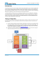
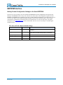
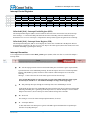
PCI-104 to PC/104 Adapter User Manual Connect Tech Inc. 42 Arrow Road Guelph, Ontario N1K 1S6 Tel: Toll: Fax: Email: Web: 519-836-1291 800-426-8979 (North America only) 519-836-4878 [email protected] [email protected] www.connecttech.com CTIM-00108 Revision 0.00 – November 16, 2012 PCI-104 to PC/104 Adapter User‟s Manual Limited Lifetime Warranty Connect Tech Inc. provides a lifetime warranty for all of our products. Should this product, in Connect Tech Inc.‟s opinion, fail to be in good working order during the warranty period, Connect Tech Inc. will, at its option, repair or replace this product at no charge, provided that the product has not been subjected to abuse, misuse, accident, disaster or non Connect Tech Inc. authorized modification or repair. You may obtain warranty service by delivering this product to an authorized Connect Tech Inc. business partner or directly to Connect Tech Inc. along with proof of purchase. Product returned to Connect Tech Inc. must be pre-authorized by Connect Tech Inc. with an RMA (Return Material Authorization) number marked on the outside of the package and sent prepaid, insured and packaged for safe shipment. Connect Tech Inc. will return this product by prepaid ground shipment service. The Connect Tech Inc. lifetime warranty is defined as the serviceable life of the product. This is defined as the period during which all components are available. Should the product prove to be irreparable, Connect Tech Inc. reserves the right to substitute an equivalent product if available or to retract lifetime warranty if no replacement is available. The above warranty is the only warranty authorized by Connect Tech Inc. Under no circumstances will Connect Tech Inc. be liable in any way for any damages, including any lost profits, lost savings or other incidental or consequential damages arising out of the use of, or inability to use, such product. Copyright Notice The information contained in this document is subject to change without notice. Connect Tech Inc. shall not be liable for errors contained herein or for incidental consequential damages in connection with the furnishing, performance, or use of this material. This document contains proprietary information that is protected by copyright. All rights are reserved. No part of this document may be photocopied, reproduced, or translated to another language without the prior written consent of Connect Tech Inc. Copyright 2012 by Connect Tech Inc. Trademark Acknowledgment Connect Tech Inc. acknowledges all trademarks, registered trademarks and/or copyrights referred to in this document as the property of their respective owners. Not listing all possible trademarks or copyright acknowledgments does not constitute a lack of acknowledgment to the rightful owners of the trademarks and copyrights mentioned in this document. Revision: 0.00 Page 2 of 19 Date: June 22, 2012 PCI-104 to PC/104 Adapter User‟s Manual Table of Contents Limited Lifetime Warranty .................................................................................................................. 2 Copyright Notice ................................................................................................................................. 2 Trademark Acknowledgment ............................................................................................................. 2 Table of Contents ................................................................................................................................ 3 Revision History .................................................................................................................................. 4 Customer Support Overview ............................................................................................................. 5 Contact Information ............................................................................................................................ 5 Introduction ......................................................................................................................................... 6 Theory of Operation ............................................................................................................................ 6 Product Features ................................................................................................................................ 7 PCI Device Information ....................................................................................................................... 8 PCI Bars .........................................................................................................................................................8 PCI Device Information ................................................................................................................................ 8 Region 4: Memory at fd000000 (32-bit, non-prefetchable) [size=16M]............8 PCI Interrupt ..................................................................................................................................................8 PC/104 (ISA) Host Interface................................................................................................................ 9 PC/104 (ISA) I/O and Memory Window Configuration (Default Starting Offsets) ............................... 9 PC/104 Transactions .................................................................................................................................. 10 IO Reads/Writes ............................................................................................................................... 10 Memory Reads/Writes ..................................................................................................................... 10 16-bit ISA I/O and Memory reads/writes, PCI Burst Writes .................................................................. 10 EEPROM Interface ............................................................................................................................ 11 Writing Custom Configuration Settings to the Serial EEPROM ........................................................... 11 PCI-104 to PC/104 Adapter Default Settings............................................................................... 11 Device Registers ............................................................................................................................... 12 BAR0 - Command, Control, Status Registers ........................................................................................ 12 BAR0 - Detailed View................................................................................................................................. 12 Interrupt Control Registers ........................................................................................................................ 13 Offset 0x00 [10:0] - Interrupt Enable Register (IER) ................................................................... 13 Offset 0x04 [10:0] - Interrupt Status Register (ISR) .................................................................... 13 Interrupt Generation ................................................................................................................................... 13 EEPROM Interface Registers ................................................................................................................... 14 Offset 0x08 [31] – EEPROM Write Start (EEP_WR) .................................................................. 14 Offset 0x0C [31] – EEPROM Write Complete (EEP_RST) ....................................................... 14 Miscellaneous Command/Configuration Register (MISC_CMD) ......................................................... 14 [1:0] - GPIO Direction Register (GPIO_DIR) ............................................................................... 14 [3:2] - Interrupt Mode Register (INT_MODE) ............................................................................... 14 [4] – Transmit FIFO trigger Setting (TX_FIFO) ............................................................................ 14 [15] – User LED (LED) .................................................................................................................... 14 PC/104 I/O Base Address Registers (BAR0, offset 0x14,0x18, 0x1C) .............................................. 15 Offset 0x14,0x18, 0x1C [15:0] – Base Address Registers (BASE_ADDR) ............................. 15 PCI-104 Connector Pinout (P6) ................................................................................................................ 16 PCI-104 Stack Position Selection .................................................................................................... 17 LED Indicators ................................................................................................................................... 17 Revision: 0.00 Page 3 of 19 Date: June 22, 2012 PCI-104 to PC/104 Adapter User‟s Manual GPIO (Digital I/O) – (Optional build) ................................................................................................ 18 Overview ...................................................................................................................................................... 18 GPIO Connector (P3) Pinout .................................................................................................................... 18 Pinout Table ...................................................................................................................................... 18 Pinout Diagram (“Left” Side View of Board) ................................................................................. 18 GPIO Operation .......................................................................................................................................... 19 Revision History Revision 0.00 Revision: 0.00 Date June 22, 2012 Author(s) Rob Callaghan Change(s) Initial Manual Revision Created. Page 4 of 19 Date: June 22, 2012 PCI-104 to PC/104 Adapter User‟s Manual Customer Support Overview If you experience difficulties after reading the manual and/or using the product, contact the Connect Tech Inc. reseller from which you purchased the product. In most cases the reseller can help you with product installation and difficulties. In the event that the reseller is unable to resolve your problem, our highly qualified support staff can assist you. Our support section is available 24 hours a day, 7 days a week on our website at: www.connecttech.com/sub/support/support.asp. See the contact information section below for more information on how to contact us directly. Our technical support is always free. Contact Information We offer three ways for you to contact us: Mail/Courier You may contact us by letter at: Connect Tech Inc. Technical Support 42 Arrow Road, Guelph, ON Canada N1K 1S6 Email/Internet You may contact us through the Internet. Our email and URL addresses on the Internet are: [email protected] [email protected] www.connecttech.com www.facebook.com/connecttechinc www.twitter.com/connecttechinc Note: Please go to the Download Zone or the Knowledge Database in the Support Center on the Connect Tech Inc. website for product manuals, installation guides, device driver software and technical tips. Submit your technical support questions to our customer support engineers via the Support Center on the Connect Tech Inc. website. Telephone/Facsimile Technical Support representatives are ready to answer your call Monday through Friday, from 8:30 a.m. to 5:00 p.m. Eastern Standard Time. Our numbers for calls are: Telephone: Telephone: Facsimile: Revision: 0.00 800-426-8979 (North America only) 519-836-1291 (Live assistance available 8:30 a.m. to 5:00 p.m. EST, Monday to Friday) 519-836-4878 (online 24 hours) Page 5 of 19 Date: June 22, 2012 PCI-104 to PC/104 Adapter User‟s Manual Introduction The Connect Tech PCI-104 to PC/104 Adapter enables testing and development of a PC/104 (ISA) peripheral card in a PCI-104 (PCI) host environment, allowing PCI-104 only systems/SBCs to include PC/104 bus peripherals in their system. Direct mapping from PCI-104 to PC/104 space allows existing PC/104 code to be moved to the PCI space with minimal code changes. The PCI-104 to PC/104 Adapter maps PCI reads/writes to ISA I/O and Memory address space, supporting 8, 16 and 32 bit reads/writes as well as PCI burst writes. A PCI driven interrupt controller allows for the enabling and disabling of all 11 PC/104 IRQ lines, transmitting detected IRQ interrupts as a single PCI interrupt with status register. A fully customizable range of I/O addresses translates 8/16/32bit PCI I/O space reads/writes to 8/16bit ISA I/O reads/writes. Another PCI memory mapped register covers the entire ISA memory address range (0x00 0000-0xFF FFFF). An on-board EEPROM is used to store these settings, loading them at system start-up. Theory of Operation The PCI-104 to PC/104 Adapter uses 4 PCI Base Address Registers (BARs) to translate PCI transactions onto the PC/104 bus architecture. Three of these BARs are used for PC/104 I/O operations, and one is used for PC/104 memory access. In order to comply with the PCI I/O space BAR size requirements, PCI I/O accesses are translated to ISA I/O accesses using one of three 256 byte (8 wide) address windows, located in three separate BARs. Any PCI Read/Write operations executed to these BARs are translated by the PCI-104 to PC/104 Adapter to PC/104 Read/Write Operations at the BARs specific I/O Address Offset. Starting offsets of these address windows can be configured via the adapters configuration register set. PCI Memory accesses are translated to ISA memory accesses using a 16Mb (24 wide) memory mapped window. The entire ISA memory space is mapped into the PCI memory space. Revision: 0.00 Page 6 of 19 Date: June 22, 2012 PCI-104 to PC/104 Adapter User‟s Manual Product Features Specification Details Form Factor PCI-104 Fully PCI 2.0 bus compliant Jumpers not required for configuration or board detection PC/104 Bus Interface PC/104 Host system interface 8 and 16 bit I/O and Memory data transfer PCI burst writes fully supported Automatic separation of 32bit PCI data into separate 8/16 bit PC/104 bus transactions. 4 Interrupt modes including PCI driven interrupt structure with Interrupt enable/disable and status registers. On-board EEPROM interface for loading of default or custom configuration on system start-up/reset. DMA operations are not supported. Digital I/O (optional) Channels: 16-bit bidirectional I/O Input/Output Ranges: Hardware selectable +3.3V or +5V(TTL/CMOS) Output Drive: High Current 24mA Controller FPGA Register Controlled Device (No jumpers needed) Custom logic available upon request Operating Temperature -40 to +85 Degrees Celsius Dimensions 3.775” x 3.550” (PC/104 Compliant) Bus PCI (PCI-104) ISA (PC/104). Software Compatibility Device can be controlled directly from a memory and I/O mapped register set in any operating system Warranty and Support Lifetime Warranty Free Technical Support Revision: 0.00 Page 7 of 19 Date: June 22, 2012 PCI-104 to PC/104 Adapter User‟s Manual PCI Device Information The PCI-104 to PC/104 Adapter has a PCI interface with 5 BAR‟s (Base Address Registers), with the following characteristics: BAR0 and BAR4 are Memory mapped; BAR1, BAR2, and BAR3 are in PCI I/O space. Byte, Word or Dword accesses, unless indicated otherwise in the details below. PCI Bars Bar Number Size (bytes) Comment(s) “0” (zero) 64K Configuration registers, used to modify and retrieve configuration info for PC/104 and EEPROM interfaces. GPIO configuration and data is also in the BAR0 register bank. Accessed as Dwords only, Register configuration below. “1” (one) 256 ISA I/O BAR_1 “2” (two) 256 ISA I/O BAR_2 “3” (three) 256 ISA I/O BAR_3 “4” (four) 16M MEM_BAR, mapped directly to ISA Memory Address space. PCI Device Information The PCI-104 to PC/104 Adapter will have the following properties in a PCI system. ID Value Comment(s) Vendor 0x12C4 Connect Tech Inc. PCI ID Device 0x1400 The PCI-104 to PC/104 Adapter Device ID Revision 0x41 (“A”) Revision of FPGA firmware Sub Vendor 0x12C4 Connect Tech Inc‟s ID Sub Device 0x1400 The ID for this board assembly Base Class 0x06 “Bridge Devices” Sub Class 0x80 “Other bridge device” Interface 0x00 Below is the output from the lspci utility in Linux with a PCI-104 to PC/104 Adapter installed in the system: 02:00.0 Bridge [0680]: Connect Tech Inc Device [12c4:1400] (rev 41) Subsystem: Connect Tech Inc Device [12c4:0000] Control: I/O+ Mem+ BusMaster- SpecCycle- MemWINV- VGASnoop- ParErr- SteppingSERR- FastB2B- DisINTxStatus: Cap+ 66MHz- UDF- FastB2B- ParErr- DEVSEL=slow >TAbort- <TAbort<MAbort- >SERR- <PERR- INTxInterrupt: pin A routed to IRQ 5 Region 0: Memory at feaf0000 (32-bit, non-prefetchable) [size=64K] Region 1: I/O ports at df00 [size=256] Region 2: I/O ports at de00 [size=256] Region 3: I/O ports at dd00 [size=256] Region 4: Memory at fd000000 (32-bit, non-prefetchable) [size=16M] PCI Interrupt The PCI-104 to PC/104 Adapter operates as a “Single function” PCI device, and therefore the card implements one interrupt, located on the INTA# signal of the PCI Bus. The interrupt is driven from multiple maskable IRQ sources from within the FPGA. The Interrupt Enable Register (IER) is used to enable the detection of the 11 PC/104 IRQ lines and generate the corresponding PCI Interrupt. Refer to the Interrupt Control section below for further details. Revision: 0.00 Page 8 of 19 Date: June 22, 2012 PCI-104 to PC/104 Adapter User‟s Manual PC/104 (ISA) Host Interface The Default I/O Address Windows allow PCI I/O space accesses to be translated into PC104 (ISA) bus accesses at three commonly used I/O ranges: 0x100-0x1FF (BAR1), 0x200-0x2FF (BAR2), and 0x300-0x3FF (BAR3). If PC/104 transactions are required at address ranges outside of these three ranges the BASE_ADDR register must be set to a new base address value. To keep the new custom settings consistent at reset and system start-up, the new setting(s) must be written to the on board EEPROM. More information on writing to the EEPROM can be found in the EEPROM Interface Registers section of the manual. PC/104 (ISA) I/O and Memory Window Configuration (Default Starting Offsets) ISA I/O Space Default Configuration BAR1 BASE_ADDR_1 ISA Memory Space Default Configuration 256K BAR4 16M 0x100 0x100-0x1FF BAR2 BASE_ADDR_2 256K 0x200 0x200-0x2FF BAR3 BASE_ADDR_3 0x00 0000 - 0xFF FFFF 256K 0x300 0x300-03FF Revision: 0.00 Page 9 of 19 Date: June 22, 2012 PCI-104 to PC/104 Adapter User‟s Manual PC/104 Transactions IO Reads/Writes PCI Base Address Registers (BARs) 1, 2, and 3 each map to a configurable 256 byte address space. Reads and writes to this offset are translated into PC/104 (ISA) transactions at the BASE_ADDR_1, BASE_ADDR_2, and BASE_ADDR_3 register values, whose defaults are 0x100, 0x200, and 0x300. The base address register is fully customizable and can be set in the range of 0x00XX to 0xFFXX. (Note: Any values in the lower register byte are ignored by the card, and are therefore labelled as „X‟ ) Pseudo Code Example: (default settings) : Existing code that writes to ISA I/O space: outb (0x308, FF); Will now be written to BAR3_BASE_ADDRESS + (IO_ADDR ^ BASE_ADDR_3) In the case of BAR3_BASE_ADDRESS being assigned I/O space by the host system at 9C00: outb(0x9C08, FF); Memory Reads/Writes PCI Base Address Register 4 maps the entire 16M of ISA memory space (0x00 0000-0xFF FFFF). Reads and writes to this BAR are translated into PC/104 (ISA) memory reads/writes at the same corresponding address. Pseudo Code Ex (default settings) : Existing code that writes to ISA memory space: mem_write (0xAB0000, FF); Will now be written to BAR4_BASE_ADDRESS + MEM_ADDR In the case of BAR3_BASE_ADDRESS being assigned Memory mapped space by the host system at 0xDB020000: mem_write (0xDBAD0000, FF); 16-bit ISA I/O and Memory reads/writes, PCI Burst Writes If the PC/104 device supports 16bit communications, and there is sufficient data available, then the PCI-104 to PC/104 Adapter will perform a 16bit operation. The adapter automatically determines if the device can support 16 bit transfers, no user input is necessary to implement this feature. PCI burst writes are also fully supported by the adapter and are split into the necessary number of PC/104 bus transfers automatically. Revision: 0.00 Page 10 of 19 Date: June 22, 2012 PCI-104 to PC/104 Adapter User‟s Manual EEPROM Interface Writing Custom Configuration Settings to the Serial EEPROM The PCI-104 to PC/104 Adapter uses an on board serial EEPROM to load its configuration at boot/system reset. Writing to the EEPROM write bit at any time will write the current values of the configuration registers into the EEPROM. An EEPROM write complete bit as well as a rapidly blinking LED indicates a successful write. The PCI104 to PC/104 Adapter is pre-loaded with default setting to cover the most commonly used PC/104 I/O ranges (0x100-0x1FF, 0x200-0x2FF, 0x300-0x3FF) but can be customized to cover any 256 byte range. For register description see the EEPROM Register section of the manual. The PCI-104 to PC/104 Adapter’s default register settings are below. PCI-104 to PC/104 Adapter Default Settings Register Name Address Offset Default Value INT_ENABLE 0x04 0x00000000 (all disabled) MISC_CMD 0x10 0x00008000 (LED off, GPIO 1-16 output, interrupt mode „00‟, TX FIFO 512) ISA_IO_BASE_1 0x14 0x100 ISA_IO_BASE_2 0x18 0x200 ISA_IO_BASE_3 0x1C 0x300 Revision: 0.00 Page 11 of 19 Date: June 22, 2012 PCI-104 to PC/104 Adapter User‟s Manual Device Registers BAR0 - Command, Control, Status Registers These registers provide the complete control and operation of the Adapter. All registers are accessed as Dwords (32 bits) only. Register Name Register Description Address Offset (Hex) Access ISR Interrupt Status/Source Register 0x00 R/W IER Interrupt (IRQ) Enable/Disable Register 0x04 R/W GPIO_OUT GPIO Output Register 0x08 R/W GPIO_IN GPIO Input register 0x0C RO MISC_CMD Miscellaneous Command/Configuration register 0x10 R/W ISA_IO_BASE_1 BAR1 I/O Base Address Register 0x14 R/W ISA_IO_BASE_2 BAR2 I/O Base Address Register 0x18 R/W ISA_IO_BASE_3 BAR3 I/O Base Address Register 0x1C R/W R/W RO Read or Write, unused bits are ignored on write, and return zero‟s on read. Read only, unused bits return zero‟s BAR0 - Detailed View Revision: 0.00 Page 12 of 19 Date: June 22, 2012 PCI-104 to PC/104 Adapter User‟s Manual Interrupt Control Registers 0x00 ISR 0x04 IER IRQ15 10 IRQ14 9 IRQ12 8 IRQ11 7 IRQ10 6 INT STATUS IRQ9 5 IRQ7 4 IRQ6 3 IRQ5 2 IRQ4 1 IRQ3 0 IRQ15 10 IRQ14 9 IRQ12 8 IRQ11 7 IRQ10 6 INT ENABLE IRQ9 5 IRQ7 4 IRQ6 3 IRQ5 2 IRQ4 1 IRQ3 0 Offset 0x00 [10:0] - Interrupt Enable Register (IER) The Interrupt Enable Register (IER) is used to enable the detection of the connected PC/104 (ISA) interrupt lines. Writing a „1‟ to the desired IRQ will enable the detection of that IRQ, when an enabled interrupt is detected the PCI-104 to PC/104 Adapter will update the interrupt status register and generate a PCI interrupt. Offset 0x04 [10:0] - Interrupt Status Register (ISR) The Interrupt Status Register (ISR) is used to display the current state of enabled PC/104 IRQ lines. When a PCI interrupt is generated by the PCI-104 to PC/104 Adapter this 32bit register (Bar 0 offset 0x00) can be read to indicate which IRQ is generating the interrupt. Interrupt Generation Two configuration bits within the BAR0 MISC_CMD register (BAR0, offset 0x10 bits 3:2) control the adapter‟s interrupt mode. „00‟ - PCI interrupt generation of detected and enabled IRQ lines with status register output (default) Upon the detection of an enabled IRQ interrupt, the PCI interrupt is driven low. The Interrupt Status Register (ISR, BAR0 reg 0x00) can then be read to indicate which interrupt is active and needs servicing. Writing a „1‟ back to the active bit in the status register will clear the interrupt. Note: PC/104 IRQ signals are edge-triggered, to avoid “stuck” IRQ signals the status register bit will only be cleared if a „1‟ is written and the IRQ is no longer active (logic high). „01‟ - IRQ interrupt direct pass through, PCI interrupt clears once enabled IRQ is cleared In this mode the detection of an enabled IRQ interrupt will still trigger the PCI interrupt, with the ISR indicating which IRQ line is generating the interrupt. However, once the interrupt is serviced and the IRQ becomes inactive, the PCI interrupt is cleared without writing back to the ISR. „10‟ – Reserved This setting is reserved for future interrupt implementations, do not use. „11‟ – Interrupts disabled In this mode all PC/104 interrupts are ignored. The IER is ignored and ISR does not update upon detection of any IRQ interrupts. Revision: 0.00 Page 13 of 19 Date: June 22, 2012 PCI-104 to PC/104 Adapter User‟s Manual EEPROM Interface Registers Offset 0x08 [31] – EEPROM Write Start (EEP_WR) This bit initiates a write operation to the EEPROM. When set to „1‟, the PCI-104 to PC/104 Adapter will write the current values of the configuration registers into the EEPROM. After the write is complete the EEPROM write complete bit will be set high (BAR0 offset 0x0C bit 31) and the „heartbeat‟ LED will blink more rapidly. Offset 0x0C [31] – EEPROM Write Complete (EEP_RST) When a write operation is initiated by setting the EEP_WR bit, the PCI-104 to PC/104 Adapter will write a „1‟ to this bit to indicate the write has completed. In addition to this bit being set, the „heartbeat‟ LED will blink more rapidly. Once the write complete has been set another EEPROM write will not occur until a „0‟ is written back to the „EEPROM write start‟ bit. The LED will also continue to blink rapidly until the EEP_WR bit is set back to „0‟. Miscellaneous Command/Configuration Register (MISC_CMD) 0x10 LED MISC_CMD 15 14 13 12 11 Reserved (DNC) 10 9 8 INT_MODE TX_FIFO 7 6 5 4 3 GPIO_DIR 2 1 [1:0] - GPIO Direction Register (GPIO_DIR) Used to control the direction of the Digital I/O. For more information regarding the GPIO_DIR register please see the GPIO section of the manual. [3:2] - Interrupt Mode Register (INT_MODE) Used to set the interrupt mode for the Adapter. For more information regarding this mode see the Interrupt Generation section of the manual. [4] – Transmit FIFO trigger Setting (TX_FIFO) The PCI-104 to PC/104 Adapter uses an internal TX FIFO which can be set to use a 128 or 512 trigger. Bit 4 of the MISC_CMD register (BAR0, offset 0x10) can be used to change this setting from its default (set to „0‟ – 512). Changing to the 128 Dword trigger will reduce throughput but decrease the worst-case PC/104 read wait time. In most cases it is best to leave this set to „0‟. [15] – User LED (LED) This bit controls the User LED. See the LED Indicators section for location and other info. Revision: 0.00 Page 14 of 19 Date: June 22, 2012 0 PCI-104 to PC/104 Adapter User‟s Manual PC/104 I/O Base Address Registers (BAR0, offset 0x14,0x18, 0x1C) Offset 0x14,0x18, 0x1C [15:0] – Base Address Registers (BASE_ADDR) The value of the BASE_ADDR registers is used to indicate the base address value that the PC/104 bus will perform read/write operations. Only the upper byte is used by the PCI-104 to PC/104 Adapter, allowing a base address setting from 0x0000-0xFF00, enabling a 256 byte address range (ex: setting 0x0000 gives a range of 0x0000-0x00FF, setting 0xFF00 enables a range of 0xFF00-0xFFFF PCI-104 Information). Revision: 0.00 Page 15 of 19 Date: June 22, 2012 PCI-104 to PC/104 Adapter User‟s Manual PCI-104 Connector Pinout (P6) Connector P6 is connects to the PCI-104 bus, a full listing of the pinout of the connector is found in the table below. Revision: 0.00 Page 16 of 19 Date: June 22, 2012 PCI-104 to PC/104 Adapter User‟s Manual PCI-104 Stack Position Selection The following PCI signals, (INTA#, INTB# INTC# INTD#), (CLK0, CLK1,CLK2, CLK3), (IDSEL0, IDSEL1, IDSEL2, IDSEL3), are selected by using the rotary switch or jumper block (optionally installed) on the PCI-104 to PC/104 Adapter board (J1 / RSW1). Selections need to match the stack location of the PCI-104 to PC/104 Adapter in your PCI-104 stack. See the table below for more details. Stack Location Rotary Switch Setting Jumper Block Setting PCI INT# PCI CLK PCI IDSEL 0,4,8,C INTA# CLK0 IDSEL0 1,5,9,D INTB# CLK1 IDSEL1 2,6,A,E INTC# CLK2 IDSEL2 3,7,B,F INTD# CLK3 IDSEL3 LED Indicators The PCI-104 to PC/104 Adapter has 2 indicator LEDs as shown below. LED D3 is the “heartbeat” indicator, the LED should flash on and off continuously to indicate the PCI-104 to PC/104 Adapter is operating properly. LED D2 is intended for user configuration and testing and it is directly mapped to MISC_CMD register (offset 0x10) Bit 15. D3 – PCI-104 to PC/104 Adapter “Heartbeat” D2 – User LED (Mapped to MISC_CMD REG Bit 15) If LED D3 is not flashing at all times when the PCI-104 to PC/104 Adapter is powered up please contact Connect Tech Technical Support ([email protected]). Revision: 0.00 Page 17 of 19 Date: June 22, 2012 PCI-104 to PC/104 Adapter User‟s Manual GPIO (Digital I/O) – (Optional build) Overview The PCI-104 to PC/104 Adapter has an optionally populated 16-bits of bi-directional GPIO that can be configured to operate with +3.3V or +5V logic levels. The upper and lower 8 bytes (GPIO0–GPIO7 = lower | GPIO8GPIO15=upper) can be set to either inputs or outputs independently. GPIO Connector (P3) Pinout Connector Location Pinout Table GND GPIO14 GPIO12 GND GPIO10 GPIO8 GND GPIO6 GPIO4 GND GPIO2 GPIO0 GND 1 3 5 7 9 11 13 15 17 19 21 23 25 2 4 6 8 10 12 14 16 18 20 22 24 26 GND GPIO13 GPIO15 GND GPIO11 GPIO9 GND GPIO7 GPIO5 GND GPIO3 GPIO1 GND Pinout Diagram (“Left” Side View of Board) Revision: 0.00 Page 18 of 19 Date: June 22, 2012 PCI-104 to PC/104 Adapter User‟s Manual GPIO Voltage Selection Jumper J2 GPIO Operation The GPIO operation on the Xtreme I/O ADC-DAC is directly controlled via 3 registers: GPIO_OUT, GPIO_IN and GPIO-MISC_CMD. The register GPIO_OUT at offset 0x0C will set the state of any GPIO pins that are set to outputs. The register GPIO_IN at offset 0x10 will contain the current state of any the GPIO pins that are set to inputs. Any pins that are set to outputs will read a zero value. The input/output directions of the GPIO bits are controlled via the GPIO-MISC_CMD register at offset 0x14. GPIO OUTPUT Register (offset 0x08) GPIO OUTPUT Reserved 31 30 29 28 27 26 25 24 23 22 21 20 19 18 17 16 15 14 13 12 11 10 9 8 7 6 5 4 3 2 1 0 4 3 2 1 0 GPIO INPUT Register (offset 0x0C) GPIO INPUT Reserved 31 30 29 28 27 26 25 24 23 22 21 20 19 18 17 16 15 14 13 12 11 10 9 8 7 6 5 Note: Each bit corresponds to the GPIO signal on the connector, IE bit-0 = GPIO0 and bit-9 = GPIO9 GPIO-MISC_CMD Register (offset 0x10) 0x10 MISC_CMD GPIO_DIR 1 0 GPIO0-7 or GPIO8-15 = 0 = OUTPUTS GPIO0-7 or GPIO8-15 = 1 = INPUTS GPIO Operation Pseudo Code Example A In this example we will set all the GPIO to outputs and the switch all GPIO signals from low to high. //setup GPIO directions write DWord 0x00000000 to offset 0x10 //set all GPIO signals low write DWord 0x00000000 to offset 0x08 //set all GPIO signals high write DWord 0x0000FFFF to offset 0x08 GPIO Operation Pseudo Code Example B In this example we will set GPIO0-7 as inputs and GPIO8-15 as outputs, then we will read the GPIO inputs. //setup GPIO directions write DWord 0x00000001 to offset 0x10 //read GPIO signals status GPIO inputs = read Word at offset 0x0C Revision: 0.00 Page 19 of 19 Date: June 22, 2012