1
Meeting 5
Summer 2009 Doing DSP Workshop
Today:
◮
Lab exercise 2 exercise VHDL.
◮
Linear systems.
◮
Transforms.
◮
Aliasing.
Education is when you read the fine print. Experience is what you get if you don’t.
– Pete Seeger
Doing DSP Workshop – Summer 2009
Meeting 5 – Page 1/56
Tuesday – May 19, 2009
An option
This Workshop can be used to get EECS 499 credit in the Fall.
This would be optional. Five people have expressed an interest.
The Workshop does not have any homework, exams nor any lab
reports. Grade would be based on a project. Could be team
effort. Base credits would be 2 hours. Could be fewer or more.
Details would need to be worked out.
As we work our way through the lab exercises give thought to
project possibilities.
Would like to have a poster/demo show-and-tell activity early in
the fall term. Would like credit and non-credit projects to
participate.
Doing DSP Workshop – Summer 2009
Meeting 5 – Page 2/56
Tuesday – May 19, 2009
Check out
fpga4fun.com
The posters on display in the EECS atrium today and likely
tomorrow. They illustrate the type of research work being done
in the department by students and faculty.
Doing DSP Workshop – Summer 2009
Meeting 5 – Page 3/56
Tuesday – May 19, 2009
Two very good Doing DSP books
I’ve added Richard Lyons book Understanding Digital Signal
Processing 2nd edition to the non-required book list on the
Workshop web page. Prentice-Hall 2004.
We won’t actually be using it, however, it is a very good read
and if you have some uncommitted money it is a very
worthwhile investment. You can occasionally find it at Borders.
Of course, there is always amazon.com.
Lyons has also collected together a set of notes from the IEEE
Digital Signal Processing Magazine into the book Streamlining
Digital Signal Processing, IEEE Press (Wiley-Interscience). These
are at a tutorial and applied level. Highly recommended.
Doing DSP Workshop – Summer 2009
Meeting 5 – Page 4/56
Tuesday – May 19, 2009
Change of emphasis
First three labs will focus on the Spartan-3 FPGA.
Second three labs will focus on the Piccolo.
A few MSP430 boards will be obtained for those who wish to
investigate MSP430. No structured lab exercises are planned.
We are giving up breadth on three devices for additional depth on two.
Doing DSP Workshop – Summer 2009
Meeting 5 – Page 5/56
Tuesday – May 19, 2009
Exercise 1 focus
Exercise 1 — Spartan-3 Starter Board
◮
Introduce ISE and Impact.
◮
Basic Spartan-3 Starter Board peripherals.
◮
VHDL. . . hardware design language.
◮
Constraint file. . . interface between VHDL and FPGA pins.
◮
Practice.
Doing DSP Workshop – Summer 2009
Meeting 5 – Page 6/56
Tuesday – May 19, 2009
Exercise 2 focus
Exercise 2 – S3SB Analog in, analog out.
◮
Use D/A driver and DA2 to generate ramps.
◮
Implement synthesizer to generate sine wave D/A out.
◮
1 bit-D/A delta sigma modulator implementation at 0 Hz.
◮
Single supply level-shift op-amp circuit.
◮
Use drivers to do A/D in to D/A out.
◮
Combine A/D-D/A with delta-sigma DAC.
Doing DSP Workshop – Summer 2009
Meeting 5 – Page 7/56
Tuesday – May 19, 2009
Exercise 3 focus
Exercise 3 – S3SB filter implementation.
◮
Single stage of all-pass filter.
◮
Cascade of above.
◮
Bit-serial multiply-and-accumulate unit.
◮
Bit-serial FIR filter implementation.
◮
Transfer function measurement.
New. Subject to change.
Doing DSP Workshop – Summer 2009
Meeting 5 – Page 8/56
Tuesday – May 19, 2009
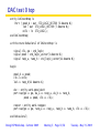
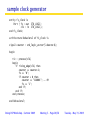
DACtest0
Generates two ramps, one per PMod D/A for viewing on
oscilloscope.
Top level connects the ramp generator with the D/A driver.
A first simple practice test illustrating D/A driver use.
Doing DSP Workshop – Summer 2009
Meeting 5 – Page 9/56
Tuesday – May 19, 2009
And the DA2 pins are . . .
The DA2 block diagram copied from the user’s manual did not include actual pin
numbers. These are given below.
The DA2 input pins (FPGA side) are:
pin
1
2
3
4
5
6
function
SYNC
DINA
DINB
SCLK
GND
VCC
The DA2 output pins (Top side) are:
pin
1
2
3
4
5
6
function
DAC0 output
no connection
DAC1 output
no connection
GND
VCC
Doing DSP Workshop – Summer 2009
Meeting 5 – Page 10/56
Tuesday – May 19, 2009
PMod DA2 port description
entity pmod_dac0 is
Port ( go : in STD_LOGIC;
da_a : in STD_LOGIC_VECTOR (11 downto 0);
da_b : in STD_LOGIC_VECTOR (11 downto 0);
pmod : out STD_LOGIC_VECTOR (3 downto 0);
clk : in STD_LOGIC);
end pmod_dac0;
◮
Leading edge of go copies contents of da_a and da_b into the two
DACs. There is a latency of about 32 clock cycles.
◮
da_a and da_b are unsigned, 0 goes to 0 volts, 4095 goes to Vcc .
◮
Set of four lines to be connected to PModD module.
◮
Max clock is 60 MHz. Counted down by a factor of 2 to clock data.
Typically use with 50 MHz or 40 MHz clock.
◮
Module is assumed to be in MIB J7 which has name pmod_d.
Doing DSP Workshop – Summer 2009
Meeting 5 – Page 11/56
Tuesday – May 19, 2009
DAC test 0 top
entity DACtest0top is
Port ( pmod_d : out STD_LOGIC_VECTOR (3 downto 0);
led : out STD_LOGIC_VECTOR (7 downto 0);
mclk : in STD_LOGIC);
end DACtest0top;
architecture Behavioral of DACtest0top is
signal clk, go : std_logic;
signal pmod : std_logic_vector(3 downto 0);
signal ramp_a, ramp_b : std_logic_vector(11 downto 0);
begin
pmod_d <= pmod;
clk <= mclk;
led <= ramp_b(11 downto 4);
dac : entity work.pmod_dac0
port map(go => go, da_a => ramp_a, da_b => ramp_b,
pmod => pmod, clk => clk);
ramper : entity work.rampgen
port map(go => go, ramp_a => ramp_a, ramp_b => ramp_b, clk => clk);
end Behavioral;
Doing DSP Workshop – Summer 2009
Meeting 5 – Page 12/56
Tuesday – May 19, 2009
The ramp generator counters
entity rampgen is
Port ( go : out STD_LOGIC;
ramp_a : out STD_LOGIC_VECTOR (11 downto 0);
ramp_b : out STD_LOGIC_VECTOR (11 downto 0);
clk : in STD_LOGIC);
end rampgen;
architecture Behavioral of rampgen is
signal a_ramp, b_ramp : std_logic_vector(11 downto 0);
signal counter : std_logic_vector(5 downto 0); -- 6 bits
begin
ramp_a <= a_ramp;
ramp_b <= b_ramp;
process(clk) is
begin
if rising_edge(clk) then
counter <= counter+1;
if counter = 0 then
-- divides clock down by 64
go <= ’0’;
a_ramp <= a_ramp+1;
b_ramp <= b_ramp+3;
else
go <= ’1’;
end if;
end if;
end process;
end Behavioral;
Doing DSP Workshop – Summer 2009
Meeting 5 – Page 13/56
Tuesday – May 19, 2009
DDS for DTMF tone generation
An entity reads slide switches row/column numbers and selects FTV
values. Set only one row and one column switch at a time.
An entity divides the 50 MHz clock down to 1 MHz.
Uses two phase accumulators to generate ROM addresses.
ROM contains 256 samples of one period of a sine wave. A block ram
was initialized using table values generated using a MATLAB script.
Doing DSP Workshop – Summer 2009
Meeting 5 – Page 14/56
Tuesday – May 19, 2009
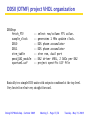
DDS0 (DTMF) project VHDL organization
DDS0top
fetch_FTV
sample_clock
DDS0
DDS1
sine_table
pmod_DA2_module
spartan3.ucf
--------
select row/column FTV value.
generates 1 MHz update clock.
DDS phase accumulator
DDS phase accumulator
sine rom, dual port
DA2 driver VHDL, 2 DACs per DA2
project specific UCF file
Basically two simple DDS units with outputs combined at the top level.
Very brute force but very straight forward.
Doing DSP Workshop – Summer 2009
Meeting 5 – Page 15/56
Tuesday – May 19, 2009
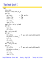
Top level (part 1)
begin
clk <= mclk;
fetch_ftv : entity work.get_ftv
port map(
swt => swt,
-- slide switches
FTV0 => FTV0,
-- FTV0
FTV1 => FTV1,
-- FTV1
clk => clk,
reset => ’0’);
sample_clock : entity fs_clock
port map (
fs => fs,
clk => clk);
DDS0 : entity work.DDS
port map (
FTV => FTV0,
-- FTV value to be used by DDS channel 0
ROM_address => address_a,
fs => fs,
clk => clk,
reset => ’0’);
DDS1 : entity work.DDS
port map (
FTV => FTV1,
-- FTV value to be used by DDS channel 1
ROM_address => address_b,
fs => fs,
clk => clk,
reset => ’0’);
Doing DSP Workshop – Summer 2009
Meeting 5 – Page 16/56
Tuesday – May 19, 2009
Top level (part 2)
sine_table_a : entity work.sine_rom
port map (
address_a => address_a,
data_a => sine_a,
address_b => address_b,
data_b => sine_b,
clk => clk);
pmod_DA2_module : entity work.pmod_dac0
port map (
da_a => sine_a(15 downto 4), -- truncating!
da_b => sine_b(15 downto 4), -- truncating!
go => not fs,
pmod => pmod_d,
clk => clk);
end Behavioral;
Doing DSP Workshop – Summer 2009
Meeting 5 – Page 17/56
Tuesday – May 19, 2009
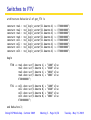
Switches to FTV
architecture Behavioral of get_FTV is
constant
constant
constant
constant
constant
constant
constant
constant
row1
row2
row3
row4
col1
col2
col3
col4
:
:
:
:
:
:
:
:
std_logic_vector(31
std_logic_vector(31
std_logic_vector(31
std_logic_vector(31
std_logic_vector(31
std_logic_vector(31
std_logic_vector(31
std_logic_vector(31
downto
downto
downto
downto
downto
downto
downto
downto
0)
0)
0)
0)
0)
0)
0)
0)
:=
:=
:=
:=
:=
:=
:=
:=
X"00000000";
X"00000000";
X"00000000";
X"00000000";
X"00000000";
X"00000000";
X"00000000";
X"00000000";
begin
FTV0 <= row1 when swt(7
row2 when swt(7
row3 when swt(7
row4 when swt(7
X"00000000";
downto
downto
downto
downto
4)
4)
4)
4)
=
=
=
=
"1000"
"0100"
"0010"
"0001"
else
else
else
else
FTV1 <= col1 when swt(3
col2 when swt(3
col3 when swt(3
col4 when swt(3
X"00000000";
downto
downto
downto
downto
0)
0)
0)
0)
=
=
=
=
"1000"
"0100"
"0010"
"0001"
else
else
else
else
end Behavioral;
Doing DSP Workshop – Summer 2009
Meeting 5 – Page 18/56
Tuesday – May 19, 2009
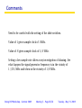
Comments
◮
Determining the row and column values are part of the
exercise.
◮
The two tones could be combined after the DACs using a
summing analog op-amp.
◮
Will combine ROM outputs digitally. Need to worry about
overflow when adding ROM output values together. Easy
step is to sign extend values by one bit then sum.
Doing DSP Workshop – Summer 2009
Meeting 5 – Page 19/56
Tuesday – May 19, 2009
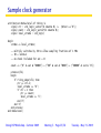
sample clock generator
entity fs_clock is
Port ( fs : out
clk : in
end fs_clock;
STD_LOGIC;
STD_LOGIC);
architecture Behavioral of fs_clock is
signal counter : std_logic_vector(5 downto 0);
begin
tic : process(clk)
begin
if rising_edge(clk) then
counter <= counter-1;
fs <= ’0’;
if counter = 0 then
counter <= "110001"; -- 49
fs <= ’1’;
end if;
end if;
end process;
end Behavioral;
Doing DSP Workshop – Summer 2009
Meeting 5 – Page 20/56
Tuesday – May 19, 2009
Basic DDS
entity DDS is
Port ( FTV : in STD_LOGIC_VECTOR (31 downto 0);
ROM_address : out std_logic_vector(7 downto 0);
fs : in STD_LOGIC;
clk : in STD_LOGIC;
reset : in std_logic);
end DDS;
architecture Behavioral of DDS is
signal accumulator : std_logic_vector(31 downto 0);
begin
ROM_address <= accumulator(31 downto 24); -- top 8 bits
process(clk, reset)
begin
if reset = ’1’ then
elsif rising_edge(clk) then
if fs = ’1’ then
accumulator <= accumulator + FTV;
end if;
end if;
end process;
end Behavioral;
Doing DSP Workshop – Summer 2009
Meeting 5 – Page 21/56
Tuesday – May 19, 2009
Completing the DTMF
◮
Need to add the two rom values. Have to make sum one bit larger
to allow for carry. Have to sign extend the ROM values before
adding.
sum <= (sine_a(15) & sine_a) + (sine_b(15) & sine_b);
◮
Connect the top 8 bits of sum to one of the DACs.
Doing DSP Workshop – Summer 2009
Meeting 5 – Page 22/56
Tuesday – May 19, 2009
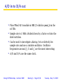
A/D in to D/A out
◮
Place PMod AD1 module in MIB J3 which is pmod_b in the
ucf file.
◮
Sample rate is 1 MHz divided down by a factor set into the
slide switches.
◮
Can be used to investigate aliasing. Set a relatively low
sample rate and use a variable oscillator. Oscillator
frequencies around fs /2 and fs are the most interesting.
◮
A/D and D/A use the same clock.
Doing DSP Workshop – Summer 2009
Meeting 5 – Page 23/56
Tuesday – May 19, 2009
A/D-D/A top (mostly)
pmod_ad1 <= pmod_b;
pmod_d <= pmod_da2;
reset <= ’0’;
-- connect PMod-AD1 module
-- connect PMod-DA2 module
timing_module : entity work.timing
port map(
strobe => strobe,
swt => swt,
clk => clk,
reset => reset);
AD_module : entity work.pmod_adc0
port map (
go => strobe,
ad_a => ad0,
ad_b => ad1,
pmod => pmod_b,
clk => clk40);
DA_module : entity work.pmod_dac0
port map (
go => strobe,
da_a => ad0,
da_b => ad1,
pmod => pmod_da2,
clk => clk);
drive_leds : entity work.led_driver
port map (
sample => ad0,
leds => led,
clk => clk);
Doing DSP Workshop – Summer 2009
Meeting 5 – Page 24/56
Tuesday – May 19, 2009
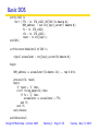
Sample clock generator
architecture Behavioral of timing is
signal ctr : std_logic_vector(13 downto 0) :=
signal count : std_Logic_vector(13 downto 0);
signal local_strobe : std_logic;
(others =>’0’);
begin
strobe <= local_strobe;
-- multiply switches by 50 to allow sampling fractions of 1 MHz
-- 50 = 32+16+2
-- no check included for swt = 0
count <= (’0’ & swt & "00000") + ("00" & swt & "0000") + ("00000" & swt & ’0’);
process(clk)
begin
if rising_edge(clk) then
ctr <= ctr-1;
local_strobe <= ’0’;
if ctr = 1 then
ctr <= count;
local_strobe <= ’1’;
end if;
end if;
end process;
end Behavioral;
Doing DSP Workshop – Summer 2009
Meeting 5 – Page 25/56
Tuesday – May 19, 2009
Comments
Need to be careful with the setting of the slide switches.
Value of 1 gives sample clock of 1 MHz.
Value of N gives sample clock of 1/N MHz.
Setting a low sample rate allows easy investigation of aliasing. See
what happen the signal generator frequency is in the vicinity of
1/(2N) MHz and when in the vicinity of 1/N MHz.
Doing DSP Workshop – Summer 2009
Meeting 5 – Page 26/56
Tuesday – May 19, 2009
One-bit DAC
Basic idea is to generate a pulse train whose average value varies with
the amplitude of a series of digital inputs. Then lowpass filter.
The resolution of the pulse widths will depend upon the clock rate and
the register sizes used.
A delta-sigma modulator is used to control the pulse sizes and
transition times to minimize the low frequency noise to the detriment
of the high frequency noise.
The high frequency noise is easily attenuated using a lowpass filter.
Doing DSP Workshop – Summer 2009
Meeting 5 – Page 27/56
Tuesday – May 19, 2009
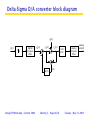
Delta-Sigma D/A converter block diagram
èxåz
óxåz
j
ÇáÖáí~ä
äçïé~ëë
ÑáäíÉê
óìxåz
óÉxåz
eEòF
Doing DSP Workshop – Summer 2009
óèxåz
NJÄáí
a^`
~å~äçÖ
äçïé~ëë
ÑáäíÉê
~å~äçÖ
çìíéìí
Éxåz
Meeting 5 – Page 28/56
Tuesday – May 19, 2009
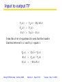
Input to output TF
Ye (z)
Yq (z)
E(z)
=
Yu (z) − H(z)E(z)
=
Yq (z) − Ye (z)
=
Ye (z)
From this of set of equations it is seen that the transfer
function between Yu (z) and Yq (z) equals 1.
Yq (z)
E(z)
Ye (z)
Doing DSP Workshop – Summer 2009
=
Q(z) + Ye (z)
=
−H(z)E(z)
=
Yq (z) − Ye (z)
Meeting 5 – Page 29/56
Tuesday – May 19, 2009
Quantization noise to output TF
Solving
E(z)
=
Ye (z)
=
Yq (z)
Q(z)
=
Ye (z)
H(z)
H(z)Yq (z)
H(z) − 1
−
1 − H(z)
In many texts H(z) = z−1 . I’m not sure that this is what is used
in practice. For this H(z) we have
E(z) = 1 − e−j2π f /fs
giving
|E(f )|2 = 4 sin2 (π f /fs ).
Doing DSP Workshop – Summer 2009
Meeting 5 – Page 30/56
Tuesday – May 19, 2009
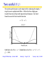
Two useful H(z)
The system performance can be improved by replacing the single z −1
stage by more sophisticated filter. A filter that has a high pass
transfer function will provide improved performance. One that I
found in an article has transfer function
z −1 (2 − z −1 ).
Magnitude
2
15
|E(f )|2
10
5
0
−500
0
Frequency (Hz)
500
Solid line is for H(z) = z −1 . Dashed line is for H(z) = z −1 (2 − z −1 ).
fr = 1000.
Doing DSP Workshop – Summer 2009
Meeting 5 – Page 31/56
Tuesday – May 19, 2009
Xilinx LogiCore Delta-Sigma
Figure Top x-ref 2
DAC Module
OPB
System
Register
Interface DACin
IPIF
Delta
Adder
A
8
Sum
OPB_Clk
RESET
SRL
FIFO
DeltaB
B
10
D
Sigma
Adder
A
Sum
Sigma
Latch
10
S
D
Q
L
L [0]
B
Q
DACout
CE
10
READ_EN
D
CE Init
10
{L [0], L [0], 0, 0, 0, 0, 0, 0, 0, 0}
CLR
L [0]
DAC_Clk_EN
Figure 2: OPB Delta-Sigma DAC Internal Block Diagram
Essentially as the “theoretical” model but modified for use with
positive valued data.
Simple RC lowpass filter used to remove the high frequency content.
Doing DSP Workshop – Summer 2009
Meeting 5 – Page 32/56
Tuesday – May 19, 2009
Comments
◮
Switching waveforms (on the board).
◮
Xilinx’s sign extension and making subtractors into adders.
◮
Wasn’t able to make the alternative H(z) to work.
◮
Design gives 8 effective bits resolution at output.
◮
Encountered “surprises”.
The A/D-D/A code allows use of an sample rate that is 1 MHz or a
submultiple. It is interesting to observe the output using 1 MHz as a
function of input sine wave frequency and also using 1/255 MHz
sample rate.
For 1 MHz sample rate my implementation works reasonably well up
to about 400 Hz.
Doing a good delta-sigma implementation or understanding why one
can’t would be a good one or two person project.
Doing DSP Workshop – Summer 2009
Meeting 5 – Page 33/56
Tuesday – May 19, 2009
Changing stride
Next week’s exercise will involve implementing a finite impulse
response (FIR) filter and one or two infinite impulse response (IIR)
filters.
Filters are typically characterized by their effect on sine waves at
various filters. Both the effect on amplitude and phase are generally of
interest.
Before we start digging into filter theory we need to lay some ground
work. More (and probably more lucid) information is contained in the
two books on the Workshop CD.
Doing DSP Workshop – Summer 2009
Meeting 5 – Page 34/56
Tuesday – May 19, 2009
Linear systems
Given two time functions x1 (t) and x( t) and a function h( )
(system) such that
y1 (t) = h[x1 (t)] and y2 (t) = h[x2 (t)]
then the system is linear if and only if
ay1 (t) + by2 (2) = h[ax1 (t) + bx2 (t)].
This leads to the principle of superposition. We can decompose
a signal into components, solve for the responses to the
individual components and then construct the overall response
by adding up the individual responses.
Nonlinear systems are not easy to work with.
Doing DSP Workshop – Summer 2009
Meeting 5 – Page 35/56
Tuesday – May 19, 2009
Stable, time invariant, causal systems
We say that a system is stable if for all bounded inputs the
system’s output is bounded.
We say that h( ) is time-invariant if for y(t) = h[x(t)] we have
y(t − τ) = h[x(t − τ)].
We say that a system is causal if the output never precedes the
input.
We will restrict our attention to linear, stable, time-invariant,
causal systems.
Doing DSP Workshop – Summer 2009
Meeting 5 – Page 36/56
Tuesday – May 19, 2009
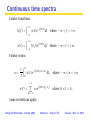
Continuous time spectra
Fourier transform:
Z +∞
X(f ) =
x(t)e−j2π f t dt
where − ∞ < f < +∞,
Z +∞
where − ∞ < t < +∞.
−∞
x(t) =
Fourier series:
cn =
1
T
Z t2
t1
X(f )ej2π f t df
−∞
x(t)e−j2π n/(t2 −t1 ) dt,
x(t) =
+∞
X
cn ej2π n/(t2 −t1 )
n=−∞
where − ∞ < n < +∞,
where t2 ≤ t < t1 .
Some restrictions apply.
Doing DSP Workshop – Summer 2009
Meeting 5 – Page 37/56
Tuesday – May 19, 2009
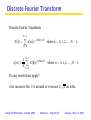
Discrete Fourier Transform
Discrete Fourier Transform:
X[k] =
x[n] =
N−1
X
x[n]e−j2π kn/N
n=0
N−1
1 X
X[k]ej2π kn/N
N k=0
where k = 0, 1, 2, . . . , N − 1.
where n = 0, 1, 2, . . . , N − 1.
Do any restrictions apply?
√
One can move the 1/N around or even use 1/ N on both.
Doing DSP Workshop – Summer 2009
Meeting 5 – Page 38/56
Tuesday – May 19, 2009
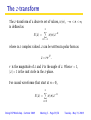
The z-transform
The z-transform of a discrete set of values, x(n), −∞ < n < ∞,
is defined as
∞
X
X(z) =
x(n)z−n
n=−∞
where is z complex valued. z can be written in polar form as
z = r ejθ .
r is the magnitude of z and θ is the angle of z. When r = 1,
|z| = 1 is the unit circle in the z-plane.
For causal waveforms (that start at n = 0),
X(z) =
Doing DSP Workshop – Summer 2009
∞
X
x(n)z−n
n=0
Meeting 5 – Page 39/56
Tuesday – May 19, 2009
The inverse z-transform
x(n) = ZT−1 [X(z)] =
1
2π j
I
X(z)zn−1 dz
C
Some methods of computation:
◮
Long division method.
◮
Partial fraction expansion method.
◮
Use of residues.
See Proakis or a similar text (or Wikipedia?) for details.
Doing DSP Workshop – Summer 2009
Meeting 5 – Page 40/56
Tuesday – May 19, 2009
Uniform sampling at rate fs
We can describes angles in the z-plane as
θ = 2π f /fs ,
where − fs /2 ≤ f < fs /2 .
Then
X(z) =
∞
X
x(n/fs )r e−2π nf /fs .
n=0
If we restrict ourselves to the unit circle then
X(z) =
∞
X
x(n/fs )e−2π nf /fs .
n=0
Why would we want to do so? It’s useful.
Doing DSP Workshop – Summer 2009
Meeting 5 – Page 41/56
Tuesday – May 19, 2009
Why use transforms?
The waveform y(t) obtained by processing a waveform, x(t), by
a LTIC system having “impulse” response, h(t), can written as
y(t) =
Zt
0
x(τ)h(t − τ)dτ .
In terms of the transforms of x(t), h(t) and y(t),
Y (f ) = H(f )X(f ) .
◮
It is often easier to think of the effects of LTIC in the
(frequency) domain than in the time domain.
◮
It is sometimes easier to operate on a waveform in the
transform domain than it is in the time domain. In spite of
the computational costs of going between domains.
Doing DSP Workshop – Summer 2009
Meeting 5 – Page 42/56
Tuesday – May 19, 2009
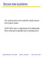
Discrete time transforms
The z-transform will be used to model filter transfer functions
in the frequency domain.
The DFT will be used as a computational tool for implementing
filters (overlap-and-xxx algorithm) and for visualizing spectra.
Doing DSP Workshop – Summer 2009
Meeting 5 – Page 43/56
Tuesday – May 19, 2009
LTI system connections
ñE=F
ÜNE=F
ÜOE=F
óE=F
ñE=F
ÜOE=F
ÜNE=F
óE=F
ñE=F
óE=F
ÜNE=F G ÜOE=F
Å~ëÅ~ÇÉ=ÅçååÉÅíáçå
ÜOE=F
ñE=F
ÜNE=F
H
ÜNE=F H ÜOE=F
ñE=F
óE=F
óE=F
é~ê~ääÉä=ÅçååÉÅíáçå
Doing DSP Workshop – Summer 2009
Meeting 5 – Page 44/56
Tuesday – May 19, 2009
Waveform spectra
A waveform’s power distribution as a function of frequency.
A real valued waveform must have a spectrum that is conjugate
symmetric around 0 Hz.
A imaginary valued waveform is not so restricted.
Obviously, real valued waveforms exist only because imaginary
valued waveforms exist ;).
For example, cos(2π f t) =
Doing DSP Workshop – Summer 2009
ej2π f t
e−j2π f t
+
.
2
2
Meeting 5 – Page 45/56
Tuesday – May 19, 2009
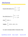
Delta functions
1
Kronecker delta function: δ[n] =
0
: n=0
+∞ :
Dirac delta function: δ(x) =
0 :
Z∞
where
δ(x)dx = 1.
x=0
−∞
Sampling:
Z∞
−∞
: n 6= 0
x 6= 0
f (x)δ(x − a)dx = f (a) .
Use context to determine whether δ is Kronecker or Dirac.
Doing DSP Workshop – Summer 2009
Meeting 5 – Page 46/56
Tuesday – May 19, 2009
A touch of reality
√
A complex number z = x + jy where j = −1 can be thought of as a
number pair of reals, z = (x, y) with well defined rules of
manipulation. For example for z0 = (a, b) and z1 = (c, d)
z0 + z1
z0 ∗ z1
=
=
(a + c, b + d)
(ac − bd, ad + bc)
The rules correspond to those of working with vectors in the plane.
The value j is a handy bookkeeping artifice.
Alternatively we can work in terms of polar coordinates:
z = r jθ = (r , θ).
z0 + z1
z0 ∗ z1
=
=
doesn’t fit in space available
(r0 r1 , θ0 + θ1 )
Of course, the above values can also be functions of time.
Doing DSP Workshop – Summer 2009
Meeting 5 – Page 47/56
Tuesday – May 19, 2009
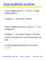
Simply bandlimited waveforms
Lowpass: Negligible energy (X(f ) = 0) for all |f | > B. Single
sided bandwidth is B.
If sampled at fs > 2B can “exactly” reconstruct.
Bandpass: Negligible energy outsize of a band, B = f2 − f1 not
containing 0 Hz.
If sampled at fs > 2B can “exactly” reconstruct. This needs to
be done very carefully, not all fs and B values necessarily work
easily.
Note that for bandpass waveforms this is not necessarily
fs > 2f2 !
Doing DSP Workshop – Summer 2009
Meeting 5 – Page 48/56
Tuesday – May 19, 2009
Frequency shifting
Consider
s(t) = a(t) cos[2π fc t+θ(t)] =
o
a(t) n j[2π fc t+θ(t)]
e
+ e−j[2π fc t+θ(t)]
2
Multiplying s(t) by e−2π fd t gives
s(t)e−2π fd t =
o
a(t) n j[2π (fc −fd )t+θ(t)]
e
+ e−j[2π (fc +fd )t+θ(t)]
2
The spectrum is shifted left by fd Hz. If it should happen that
fd = fc then
s(t)e−2π fc t =
o
a(t) n j[2π θ(t)]
e
+ e−j[4π fc t+θ(t)]
2
If we can filter out the energy around −2fc then
s(t)e−2π fc t =
Doing DSP Workshop – Summer 2009
a(t) j2π θ(t)
e
2
Meeting 5 – Page 49/56
Tuesday – May 19, 2009
Uniform time quantization & reconstruction
Analog waveform
amplitude
1
0.5
Analog
waveform.
0
−0.5
−1
0
0.2
0.4
0.6
0.8
1
−3
x 10
Time quantized waveform
amplitude
1
0.5
Time
quantized.
0
−0.5
−1
0
0.2
0.4
0.6
0.8
1
−3
Reconstructed time quantized waveformx 10
amplitude
1
0.5
Reconstructed.
0
−0.5
−1
0
0.2
0.4
0.6
time in seconds
Doing DSP Workshop – Summer 2009
0.8
1
−3
x 10
Meeting 5 – Page 50/56
Tuesday – May 19, 2009
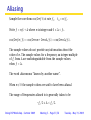
Aliasing
Sample the waveform cos(2π f t) at rate fs ,
tn = n/fs .
Write f = αfs + ∆ where α is integer and 0 ≤ ∆ < fs .
cos(2π f n/fs ) = cos(2π nα + 2π n∆/fs ) = cos(2π n∆/fs ).
The sample values do not provide any information about the
value of α. The sample values for a frequency an integer multiple
of fs from ∆ are undistinguishable from the sample values
when f = ∆.
The word alias means “known by another name”.
When α 6= 0 the sample values are said to have been aliased.
The range of frequencies aliased to is generally taken to be
−fs /2 ≤ ∆ < fs /2.
Doing DSP Workshop – Summer 2009
Meeting 5 – Page 51/56
Tuesday – May 19, 2009
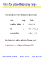
Units for aliased frequency range
Units typically used to describe aliased frequency range:
units
range
limits
nomalized radians
2π
−π ≤ ω < π
Hz
fs
−fs /2 ≤ f < fs /2
normalized Hz
1
−1/2 ≤ f < 1/2
Note the inclusion and non-inclusion of the end points.
As practitioners, we will make exclusive use of Hz!
Doing DSP Workshop – Summer 2009
Meeting 5 – Page 52/56
Tuesday – May 19, 2009
Where does “the” alias land?
Assume the base frequency range is: −fs /2 ≤ f < fs /2.
For a frequency component at fc > 0 find K such that
−fs /2 ≤ fc − Kfs < fs /2.
The energy at fc aliases to fca = fc − Kfs .
For a frequency component at fc < 0 find K such that
−fs /2 ≤ fc + Kfs < fs /2.
The energy at fc aliases to fca = fc + Kfs .
We can use aliasing to shift frequencies to “baseband”.
Doing DSP Workshop – Summer 2009
Meeting 5 – Page 53/56
Tuesday – May 19, 2009
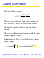
Aliasing demonstration
Using Euler’s relation we can write
cos(2π f t) =
e−j2π f t
ej2π f t
+
2
2
The movies were generated using a input frequency sweeping from 0
Hz to 24,000 Hz in 30 seconds. The sample frequency was 8 kHz.
The first movie demonstrates what happens when the cosine is
sampled.
The second movie demonstrates what happens when only the positive
frequency component is sampled.
Both movies show the effects of using a slowly increasing frequency,
(linear FM sweep).
swept sinusoid
jçîáÉ
Doing DSP Workshop – Summer 2009
swept complex exponential
Meeting 5 – Page 54/56
jçîáÉ
Tuesday – May 19, 2009
Comments on sampling
The spectrum of an sampled waveform does NOT fold.
Common practice is to make the base frequency range [−fs /2, fs /2).
The frequency fs /2 is called the Nyquist frequency.
Given a real valued lowpass spectrum with bandwidth, BW the sample
frequency equal to 2BW is often called the Nyquist sample rate.
Reality gets in the way. One should sample at a rate of at least two or
three times the Nyquist rate (not frequency).
Common sample rates:
standard telephone system
wideband telecommunications
home music CDs
professional audio
DVD-Audio
instrumentation, RF, video
Doing DSP Workshop – Summer 2009
8 kHz
16 kHz
44.1 kHz
48 kHz
192 kHz
extremely fast
Meeting 5 – Page 55/56
Tuesday – May 19, 2009
Some interesting audio frequencies
Many waveforms can have energy beyond a band of interest.
Voice:
Piano:
fundamental around 150 Hz, overtones to about 5 kHz.
male fundamental about 120 Hz.
female fundamental about 200 Hz.
bass low E is 82.4 Hz.
soprano high C is 1,046.5 Hz.
27.5 Hz (A0) to 4816 Hz (C8).
Harmonics may extend frequencies by a factor of 3 to 5 or more.
Normal young adult hearing range is 20 Hz to 20,000 Hz.
Telephone nominally passes range 300 Hz to 3200 Hz.
Doing DSP Workshop – Summer 2009
Meeting 5 – Page 56/56
Tuesday – May 19, 2009