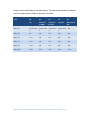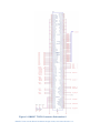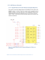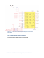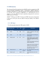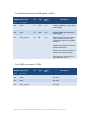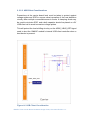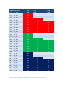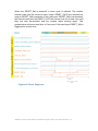
1
SMARC T335x Carrier Board Hardware Design Guide SMARC T335x Carrier Board Hardware Design Guide, Document Revision 1.3 SMARC T335x Carrier Board Hardware Design Guide, Document Revision 1.3 Revision History Revision Date Changes from Previous Revision 1.0 2013/7/26 Initial Release 1.2 2014/04/19 Update to Hardware rev. 00B0 1. Remove the 10k pull-ups on USB_EN_OC# 2. Add SDIO_PWREN Schematics 3. Rename Evaluation Carrier Board from Smartbase T3 to SMART-BEE 1.3 2014/11/05 Correct CARRIER_PWR_ON Power Rail from VDD_IN to VDD_IO SMARC T335x Carrier Board Hardware Design Guide, Document Revision 1.3 USER INFORMATION About This Manual This document provides information about products from EMBEDIAN, INC. No warranty of suitability, purpose, or fitness is implied. While every attempt has been made to ensure that the information in this document is accurate, the information contained within is supplied “as-is” and is subject to change without notice. For the circuits, descriptions and tables indicated, EMBEDIAN assumes no responsibility as far as patents or other rights of third parties are concerned. Copyright Notice Copyright © 2013 EMBEDIAN, INC.. All rights reserved. No part of this manual may be reproduced, transmitted, transcribed, stored in a retrieval system, or translated into any language or computer language, in any form or by any means (electronic, mechanical, photocopying, recording, or otherwise), without the express written permission of EMBEDIAN. Trademarks The following lists the trademarks of components used in this board. ARM is a registered trademark of ARM Limited. Android is a registered trademark of Google Linux is a registered trademark of Linus Torvalds. WinCE is a registered trademark of Microsoft TI is a registered trademark of Texas Instruments All other products and trademarks mentioned in this manual are trademarks of their respective owners. Standards EMBEDIAN is ISO 9001:2008 and ISO14001-certified manufacturer. SMARC is an SGET standard for ARM computer on module. Warranty This EMBEDIAN product is warranted against defects in material and workmanship for the warranty period from the date of shipment. During the warranty period, EMBEDIAN will at its discretion, decide to repair or replace defective products. Within the warranty period, the repair of products is free of charge as long as warranty conditions are observed. The warranty does not apply to defects resulting from improper or inadequate maintenance or handling by the buyer, unauthorized modification or misuse, operation outside of the product’s environmental specifications or improper installation or maintenance. SMARC T335x Carrier Board Hardware Design Guide, Document Revision 1.3 EMBEDIAN will not be responsible for any defects or damages to other products not supplied by EMBEDIAN that are caused by a faulty EMBEDIAN product. Technical Support Technicians and engineers from EMBEDIAN and/or its subsidiaries and official distributors are available for technical support. We are committed to making our product easy to use and will help you use our products in your systems. Before contacting EMBEDIAN technical support, please consult our Web site for the latest product documentation, utilities, and drivers. If the information does not help solve the problem, contact us by e-mail or telephone. SMARC T335x Carrier Board Hardware Design Guide, Document Revision 1.3 Table of Contents CHAPTER 1 INTRODUCTION ........................................................................................................... 10 1.1 ACRONYMS AND ABBREVIATIONS USED ............................................................................ 11 1.2 SIGNAL TABLE TERMINOLOGY ............................................................................................. 14 1.3 DOCUMENT AND STANDARD REFERENCES....................................................................... 17 1.4 INTENDED AUDIENCE ............................................................................................................... 19 CHAPTER 2 INTERFACES ................................................................................................................. 21 2.1 SMARC T335X CONNECTOR PIN MAPPING ........................................................................ 30 2.2 ETHERNET INTERFACE ............................................................................................................ 32 2.3 USB INTERFACE .......................................................................................................................... 45 2.4 PARALLEL RGB LCD INTERFACE .......................................................................................... 55 2.5 SD/SDIO INTERFACE .................................................................................................................. 71 2.6 I2S AUDIO INTERFACE .............................................................................................................. 76 2.7 CAN BUS INTERFACE................................................................................................................. 80 2.8 SERIAL COM PORT INTERFACE ............................................................................................. 85 2.9 SPI INTERFACE............................................................................................................................ 90 2.10 I2C BUS INTERFACE ................................................................................................................. 95 2.11 SELECTING THE BOOT MODE .............................................................................................. 99 2.12 WATCHDOG CONTROL SIGNALS ....................................................................................... 101 CHAPTER 3 POWER DESIGN GUIDELINE................................................................................ 104 3.1 POWER SIGNALS ...................................................................................................................... 104 3.2 RTC BATTERY ............................................................................................................................ 108 3.3 POWER FLOW AND CONTROL SIGNALS BLOCK DIAGRAM ....................................... 109 3.4 POWER STATES ......................................................................................................................... 111 3.5 POWER SEQUENCES ................................................................................................................ 112 3.6 LAYOUT REQUIREMENTS ...................................................................................................... 116 3.7 REFERENCE SCHEMATICS .................................................................................................... 117 CHAPTER 4 FLOOR PLANNING THE PCB ................................................................................ 120 4.1 CARRIER CONNECTOR ........................................................................................................... 120 4.2 MODULE AND CARRIER CONNECTOR PIN NUMBERING CONVENTION ................ 123 4.3 MODULE OUTLINE – 82MM X 50MM MODULE ................................................................ 123 4.4 MODULE “Z” HEIGHT CONSIDERATION ........................................................................... 125 4.5 CARRIER BOARD CONNECTOR PCB FOOTPRINT .......................................................... 126 4.6 MODULE AND CARRIER BOARD MOUNTING HOLES – GND CONNECTION........... 127 4.7 CARRIER BOARD STANDOFFS .............................................................................................. 127 SMARC T335x Carrier Board Hardware Design Guide, Document Revision 1.3 Using this Guide This document is a guideline for developing a carrier board hardware that confirms to the specifications for SMARC (ULP-COM) T335X computer on module. Conventions used in this guide This table describes the typographic conventions used in this guide: This Convention Is used for Italic type Emphasis, new terms, variables, and document titles. Filenames, pathnames, and code examples. monospaced type Embedian Information Document Updates Please always check the product specific section on the Embedian support website at www.embedian.com/ for the most current revision of this document. Contact Information For more information about your Embedian products, or for customer service and technical support, contact Embedian directly. To contact Embedian by Use Mail Embedian, Inc. 4F-7. 432 Keelung Rd. Sec. 1, Taipei 11051, Taiwan World Wide Web http://www.embedian.com/ Telephone + 886 2 2722 3291 SMARC T335x Carrier Board Hardware Design Guide, Document Revision 1.3 Additional Resources Please also refer to the most recent Embedian SMARC T335X user’s manual or TI AM335x processor reference manual and related documentation for additional information. SMARC T335x Carrier Board Hardware Design Guide, Document Revision 1.3 Introduction This Chapter gives background information on this document. Section includes: Acronyms and Abbreviations Used Signal Table Terminology Document and Standard References Intended Audience SMARC T335x Carrier Board Hardware Design Guide, Document Revision 1.3 Chapter 1 Introduction This document is created to guide users to design SMARC (formerly ULP-COM) compliant carrier board. It will focus only on the interfaces in SMARC T335X pinouts and related peripherals. Some interfaces like camera interface are defined in SMARC specification, but not in SMARC T335X, will not be addressed in this document. This document should be used in conjunction with the SMARC T335X user’s manual and SMART-BEE carrier schematics. This document also contains reference schematics for different interfaces. These interfaces are described in the user’s manual of SMARC T335X module. SMARC T335X module does not feature the full set of all interfaces that defined in SMARC specification. Therefore, it is strongly recommended to read the user’s manual of the SMARC T335X modules that are required to be support by the carrier board. This carrier board hardware design guide for SMARC T335X computer on module helps walk hardware designers through the various stages of designing a carrier board on this platform. Using this document, hardware designers can efficiently locate the resources they need at every step in the board design flow. An evaluation carrier SMART-BEE is available for SMARC T335X computer on module. SMART-BEE has all the interfaces on SMARC T335X module in the form of either connectors or pin headers and is a good reference for hardware designers who would like to develop their own carrier boards. All examples of this document are based on SMART-BEE carrier board that is available from Embedian. This document also provides a collection of useful documentation, application reports, and design recommendations. SMARC T335x Carrier Board Hardware Design Guide, Document Revision 1.3 1.1 Acronyms and Abbreviations Used Table below shows the acronyms and abbreviations used in this section. Abbreviation Explanation ADC Analogue to Digital Converter Auto‐MDIX Automatically Medium Dependent Interface Crossing, a PHY with Auto-MDIX f is able to detect whether RX and TX need to be crossed (MDI or MDIX) CAN Controller Area Network, a bus that is manly used in automotive and industrial environment CPU Central Processor Unit DAC Digital to Analogue Converter DDC Display Data Channel, interface for reading out the capability of a monitor DSI Display Serial Interface EDID Extended Display Identification Data, timing setting information provided by the display in a PROM EMI Electromagnetic Interference, high frequency disturbances eMMC Embedded Multi Media Card, flash memory combined with MMC interface controller in a BGA package, used as internal flash memory ESD Electrostatic Discharge, high voltage spike or spark that can damage electrostatic- sensitive devices GBE Gigabit Ethernet, Ethernet interface with a maximum data rate of 1000Mbit/s GND Ground GPIO General Purpose Input/Output, pin that can be configured being an input or output HDA High Definition Audio (HD Audio), digital audio interface between CPU and audio codec High-Definition Multimedia Interface, combines audio and video signal for connecting monitors, TV sets or Projectors, electrical compatible with DVI-D SMARC T335x Carrier Board Hardware Design Guide, Document Revision 1.3 HDMI Abbreviation Explanation I2C Inter-Integrated Circuit, two wire interface for connecting low speed peripherals I2S Integrated Interchip Sound, serial bus for connecting PCM audio data between two devices JTAG Joint Test Action Group, widely used debug interface LCD Liquid Crystal Display LSB Least Significant Bit LVDS Low-Voltage Differential Signalling, electrical interface standard that can transport very high speed signals over twisted-pair cables. Many interfaces like PCIe or SATA use this interface. Since the first successful application was the Flat Panel Display Link, LVDS became a synonymous for this interface. In this document, the term LVDS is used for the Flat Panel Display Link interface. MDI Medium Dependent Interface, physical interface between Ethernet PHY and cable connector MDIX Medium Dependent Interface Crossed, an MDI interface with crossed RX and TX interfaces MSB Most Significant Bit MXM3 Mobile PCI Express Module (second generation), graphic card standard for mobile device, the SMARC form factor uses the physical connector but not the pin-out and the PCB dimensions of the MXM3 standard. N/A Not Available N/C Not Connected OD Open Drain OTG USB On-The-Go, a USB host interface that can also act as USB client when connected to another host interface PCB Printed Circuit Board PD Pull Down Resistor SMARC T335x Carrier Board Hardware Design Guide, Document Revision 1.3 Abbreviation Explanation PHY Physical Layer of the OSI model PMIC Power Management IC, integrated circuit that manages amongst others the power sequence of a system PU Pull Up Resistor PWM Pulse-Width Modulation RGB Red Green Blue, colour channels in common display interfaces RJ45 Registered Jack, common name for the 8P8C modular connector that is used for Ethernet wiring RS232 Single ended serial port interface RS422 Differential signaling serial port interface, full duplex RS485 Differential signaling serial port interface, half duplex, multi drop configuration possible SD Secure Digital, flash memory card SDIO Secure Digital Input Output, an external bus for peripherals that uses the SD interface SOC System on a Chip, IC which integrates the main component of a computer on a single chip SPI Serial Peripheral Interface Bus, synchronous four wire full duplex bus for peripherals TVS Diode Transient-Voltage-Suppression Diode, diode that is used to protect interfaces against voltage spikes UART Universal Asynchronous Receiver/Transmitter, serial interface, in combination with a transceiver a RS232, RS422, RS485, IrDA or similar interface can be achieved USB Universal Serial Bus, serial interface for internal and external peripherals VDD Positive supply voltage VGA Video Graphics Array, analogue video interface for monitors SMARC T335x Carrier Board Hardware Design Guide, Document Revision 1.3 1.2 Signal Table Terminology Table below describes the terminology used in this section for the Signal Description tables. The “#” symbol at the end of the signal name indicates that the active or asserted state occurs when the signal is at a low voltage level. When “#” is not present, the signal is asserted when at a high voltage level. Direction Type / Tolerance Notes Input Input to the Module Output Output from the Module Output OD Open drain output from the Module Bi‐Dir Bi-directional signal (can be input or output) Bi‐Dir OD Bi-directional signal; output from the Module is open drain VDD_IN Signal may be exposed to Module input voltage range (3.35 to 5.25V) CMOS 1.8V CMOS logic input and / or output, 1.8V I/O supply level or tolerance CMOS 3.3V CMOS logic input and / or output, 3.3V I/O supply level or tolerance CMOS VDD_IO CMOS logic I/O level – set to 3.3V for SMATC T335X Modules CMOS VDD_JTAG_IO VDD_JTAG_IO is 3.3V in SMARC T335X. The JTAG emulator adjusts to the VDD_JTAG_IO level provided by the Module, on the JTAG connector GBE MDI Differential analog signaling for Gigabit Media Dependent Interface LVDS AFB LVDS signaling for AFB – may be PCIe, SATA, USB SS, GBE MDI, MLB or other low voltage high speed differential physical interface SMARC T335x Carrier Board Hardware Design Guide, Document Revision 1.3 Direction Type / Tolerance Notes LVDS LCD LVDS signaling used for LVDS LCD displays USB DC coupled differential signaling used for traditional (non- Super-Speed) USB signals USB SS LVDS signaling used for Super Speed USB 3.0 USB VBUS 5V 5V tolerant input for USB VBUS detection 10/100Base-TX Differential signaling, using MLT-3 (tri level) format for 100 MBit / Sec full duplex Ethernet REF Reference voltage output. May be sourced from a Module power plane. PDS Pull-down strap. A Module output pin that is either tied to GND or is not connected. Used to signal Module capabilities (pin-out type) to the Carrier Board. P Power input/output Schematic examples are drawn with signal directions shown per the figure below. Nets that connect to the SMARC Module are named per the SGET SMARC specification. Figure 1: Schematic Conventions SMARC T335x Carrier Board Hardware Design Guide, Document Revision 1.3 Power nets are labeled per the table below. The power rail behavior under the various system power states is shown in the table. Term S0 S3 S4 S5 G3 On Suspend to RAM Suspend to Disk Soft Off Mechanical Off VDD_IN 3.35V~5.25 V 3.35V~5.25 V 3.35V~5.25 V 3.35V~5.25 V Off VDD_50 5V Off Off Off Off VDD_33 3.3V Off Off Off Off AUD_33 3.3V Off Off Off Off VDD_18 1.8V Off Off Off Off VDD_RTC 3.0V 3.0V 3.0V 3.0V 3.0V SMARC T335x Carrier Board Hardware Design Guide, Document Revision 1.3 1.3 Document and Standard References 1.3.1. External Industry Standard Documents The I2C Specification, Version 2.1, January 2000, Philips Semiconductor (now NXP) (www.nxp.com). I2S Bus Specification, Feb. 1986 and Revised June 5, 1996, Philips Semiconductor (now NXP) (www.nxp.com). MXM3 Graphics Module Mobile PCI Express Module Electromechanical Specification, Version 3.0, Revision 1.1, © 2009 NVIDIA Corporation (www.mxm-sig.org). PICMG® EEEP Embedded EEPROM Specification, Rev. 1.0, August 2010 (www.picmg.org). SD Specifications Part 1 Physical Layer Simplified Specification, Version 3.01, May 18, 2010, © 2010 SD Group and SD Card Association (Secure Digital) (www.sdcard.org). SPI Bus – “Serial Peripheral Interface” - de-facto serial interface standard defined by Motorola. A good description may be found on Wikipedia (http://en.wikipedia.org/wiki/Serial_Peripheral_Interface_Bus). USB Specifications (www.usb.org). 1.3.2. SGET Documents SMARC_Hardware_Specification_V1p0, version 1.0, December 20, 2012. 1.3.3. Embedian Documents The following documents are listed for reference. The Module schematic is not usually available outside of Embedian, without special permission. The other schematics may be available, under NDA or otherwise. Contact your Embedian representative for more information. The SMARC T335X Evaluation Carrier schematic is particularly useful as an example of the implementation of various interfaces on a Carrier board. SMARC_T335X Evaluation Carrier Board Schematic, PDF and OrCAD format SMARC_T335X Evaluation Carrier Board User’s Manual SMARC_T335X Carrier Board Hardware Design Guide SMARC_T335X Carrier Board Hardware Layout Guide SMARC T335x Carrier Board Hardware Design Guide, Document Revision 1.3 SMARC_T335X User’s Manual SMARC_T335X Schematic Checklist 1.3.4. TI Documents AM335x ARM Cortex-A8 Microprocessors (MPUs), April 15 2013 (rev. F) AM335x Schematic Checklist, Oct 31 2011 AM335x ARM Cortex-A8 Microprocessors (MPUs) Technical References Manual, April 15 2013 (rev. H) AM335x Power Consumption Summary, Oct 31 2011 1.3.5. TI Development Tools Pin Mux Utility for ARM® Microprocessors Power Estimation Tool (PET) 1.3.6. TI Software Documents LINUXEZSDK-AM335x ANDROIDDEVKIT-JB-AM335x 1.3.7. Embedian Software Documents Embedian Linux BSP for SMARC T335X Module Embedian Android BSP for SMARC T335X Module Embedian Linux BSP User’s Guide Embedian Android BSP User’s Guide 1.3.8. TI Design Network Beaglebone Adeneo Embedded (Windows Embedded Compact 7) Nucleus QNX SMARC T335x Carrier Board Hardware Design Guide, Document Revision 1.3 1.4 Intended Audience This design guide is intended for electronics engineers and PCB layout engineers designing Carrier Boards for SMARC T335X Modules. SMARC T335x Carrier Board Hardware Design Guide, Document Revision 1.3 Interfaces This chapter describes the signals and implementation guideline found on SMARC T335X connectors. Section includes: SMARC T335X Connector Pin Mapping Ethernet Interface USB Interface Parallel RGB LCD Interface SD/SDIO Interface I2C Audio Interface CAN BUS Interface Serial COM Port Interface SPI Interface I2C BUS Interface Selecting the Boot Mode Watchdog Control Signals SMARC T335x Carrier Board Hardware Design Guide, Document Revision 1.3 Chapter 2 Interfaces There are 314 edge fingers of the SMARC module that mate with a low profile 314 pin 0.5mm pitch right angle connector (the connector is sometimes identified as a 321 pin connector, but 7 pins are lost to the key). The following table lists the module pin assignments for all 314 edge fingers. P-Pin Primary (Top) Side S-Pin Secondary (Bottom) Side S1 PCAM_VSYNC P1 PCAM_PXL_CK1 S2 PCAM_HSYNC P2 GND S3 GND P3 CSI1_CK+ / PCAM_D0 S4 PCAM_PXL_CK0 P4 CSI1_CK- / PCAM_D1 S5 I2C_CAM_CK P5 PCAM_DE S6 CAM_MCK P6 PCAM_MCK S7 I2C_CAM_DAT P7 CSI1_D0+ / PCAM_D2 S8 CSI0_CK+ / PCAM_D10 P8 CSI1_D0- / PCAM_D3 S9 CSI0_CK- / PCAM_D11 P9 GND S10 GND P10 CSI1_D1+ / PCAM_D4 S11 CSI0_D0+ / PCAM_D12 P11 CSI1_D1- / PCAM_D5 S12 CSI0_D0- / PCAM_D13 P12 GND S13 GND P13 CSI1_D2+ / PCAM_D6 S14 CSI0_D1+ / PCAM_D14 P14 CSI1_D2- / PCAM_D7 S15 CSI0_D1- / PCAM_D15 P15 GND S16 GND P16 CSI1_D3+ / PCAM_D8 S17 AFB0_OUT P17 CSI1_D3- / PCAM_D9 S18 AFB1_OUT P18 GND S19 AFB2_OUT P19 GBE_MDI3- S20 AFB3_IN SMARC T335x Carrier Board Hardware Design Guide, Document Revision 1.3 P-Pin Primary (Top) Side S-Pin Secondary (Bottom) Side P20 GBE_MDI3+ S21 AFB4_IN P21 GBE_LINK100# S22 AFB5_IN P22 GBE_LINK1000# S23 AFB6_PTIO P23 GBE_MDI2- S24 AFB7_PTIO P24 GBE_MDI2+ S25 GND P25 GBE_LINK_ACT# S26 SDMMC_D0 P26 GBE_MDI1- S27 SDMMC_D1 P27 GBE_MDI1+ S28 SDMMC_D2 P28 GBE_CTREF S29 SDMMC_D3 P29 GBE_MDI0- S30 SDMMC_D4 P30 GBE_MDI0+ S31 SDMMC_D5 P31 SPI0_CS1# S32 SDMMC_D6 P32 GND S33 SDMMC_D7 P33 SDIO_WP S34 GND P34 SDIO_CMD S35 SDMMC_CK P35 SDIO_CD# S36 SDMMC_CMD P36 SDIO_CK S37 SDMMC_RST# P37 SDIO_PWR_EN S38 AUDIO_MCK P38 GND S39 I2S0_LRCK P39 SDIO_D0 S40 I2S0_SDOUT P40 SDIO_D1 S41 I2S0_SDIN P41 SDIO_D2 S42 I2S0_CK P42 SDIO_D3 S43 I2S1_LRCK P43 SPI0_CS0# S44 I2S1_SDOUT P44 SPI0_CK S45 I2S1_SDIN SMARC T335x Carrier Board Hardware Design Guide, Document Revision 1.3 P-Pin Primary (Top) Side S-Pin Secondary (Bottom) Side P45 SPI0_DIN S46 I2S1_CK P46 SPI0_DO S47 GND P47 GND S48 I2C_GP_CK P48 SATA_TX+ S49 I2C_GP_DAT P49 SATA_TX- S50 I2S2_LRCK P50 GND S51 I2S2_SDOUT P51 SATA_RX+ S52 I2S2_SDIN P52 SATA_RX- S53 I2S2_CK P53 GND S54 SATA_ACT# P54 SPI1_CS0# S55 AFB8_PTIO P55 SPI1_CS1# S56 AFB9_PTIO P56 SPI1_CK S57 PCAM_ON_CSI0# P57 SPI1_DIN S58 PCAM_ON_CSI1# P58 SPI1_DO S59 SPDIF_OUT P59 GND S60 SPDIF_IN P60 USB0+ S61 GND P61 USB0- S62 AFB_DIFF0+ P62 USB0_EN_OC# S63 AFB_DIFF0- P63 USB0_VBUS_DET S64 GND P64 USB0_OTG_ID S65 AFB_DIFF1+ P65 USB1+ S66 AFB_DIFF1- P66 USB1- S67 GND P67 USB1_EN_OC# S68 AFB_DIFF2+ P68 GND S69 AFB_DIFF2- P69 USB2+ S70 GND SMARC T335x Carrier Board Hardware Design Guide, Document Revision 1.3 P-Pin Primary (Top) Side S-Pin Secondary (Bottom) Side P70 USB2- S71 AFB_DIFF3+ P71 USB2_EN_OC# S72 AFB_DIFF3- P72 PCIE_C_PRSNT# S73 GND P73 PCIE_B_PRSNT# S74 AFB_DIFF4+ P74 PCIE_A_PRSNT# S75 AFB_DIFF4- <Key> <Key> P75 PCIE_A_RST# S76 PCIE_B_RST# P76 PCIE_C_CKREQ# S77 PCIE_C_RST# P77 PCIE_B_CKREQ# S78 PCIE_C_RX+ P78 PCIE_A_CKREQ# S79 PCIE_C_RX- P79 GND S80 GND P80 PCIE_C_REFCK+ S81 PCIE_C_TX+ P81 PCIE_C_REFCK- S82 PCIE_C_TX- P82 GND S83 GND P83 PCIE_A_REFCK+ S84 PCIE_B_REFCK+ P84 PCIE_A_REFCK- S85 PCIE_B_REFCK- P85 GND S86 GND P86 PCIE_A_RX+ S87 PCIE_B_RX+ P87 PCIE_A_RX- S88 PCIE_B_RX- P88 GND S89 GND P89 PCIE_A_TX+ S90 PCIE_B_TX+ P90 PCIE_A_TX- S91 PCIE_B_TX- P91 GND S92 GND P92 HDMI_D2+ S93 LCD_D0 P93 HDMI_D2- S94 LCD_D1 SMARC T335x Carrier Board Hardware Design Guide, Document Revision 1.3 P-Pin Primary (Top) Side S-Pin Secondary (Bottom) Side P94 GND S95 LCD_D2 P95 HDMI_D1+ S96 LCD_D3 P96 HDMI_D1- S97 LCD_D4 P97 GND S98 LCD_D5 P98 HDMI_D0+ S99 LCD_D6 P99 HDMI_D0- S100 LCD_D7 P100 GND S101 GND P101 HDMI_CK+ S102 LCD_D8 P102 HDMI_CK- S103 LCD_D9 P103 GND S104 LCD_D10 P104 HDMI_HPD S105 LCD_D11 P105 HDMI_CTRL_CK S106 LCD_D12 P106 HDMI_CTRL_DAT S107 LCD_D13 P107 HDMI_CEC S108 LCD_D14 P108 GPIO0 / CAM0_PWR# S109 LCD_D15 P109 GPIO1 / CAM1_PWR# S110 GND P110 GPIO2 / CAM0_RST# S111 LCD_D16 P111 GPIO3 / CAM1_RST# S112 LCD_D17 P112 GPIO4 / HDA_RST# S113 LCD_D18 P113 GPIO5 / PWM_OUT S114 LCD_D19 P114 GPIO6 / TACHIN S115 LCD_D20 P115 GPIO7 / PCAM_FLD S116 LCD_D21 P116 GPIO8 / CAN0_ERR# S117 LCD_D22 P117 GPIO9 / CAN1_ERR# S118 LCD_D23 P118 GPIO10 S119 GND SMARC T335x Carrier Board Hardware Design Guide, Document Revision 1.3 P-Pin Primary (Top) Side S-Pin Secondary (Bottom) Side P119 GPIO11 S120 LCD_DE P120 GND S121 LCD_VS P121 I2C_PM_CK S122 LCD_HS P122 I2C_PM_DAT S123 LCD_PCK P123 BOOT_SEL0# S124 GND P124 BOOT_SEL1# S125 LVDS0+ P125 BOOT_SEL2# S126 LVDS0- P126 RESET_OUT# S127 LCD_BKLT_EN P127 RESET_IN# S128 LVDS1+ P128 POWER_BTN# S129 LVDS1- P129 SER0_TX S130 GND P130 SER0_RX S131 LVDS2+ P131 SER0_RTS# S132 LVDS2- P132 SER0_CTS# S133 LCD_VDD_EN P133 GND S134 LVDS_CK+ P134 SER1_TX S135 LVDS_CK- P135 SER1_RX S136 GND P136 SER2_TX S137 LVDS3+ P137 SER2_RX S138 LVDS3- P138 SER2_RTS# S139 I2C_LCD_CK P139 SER2_CTS# S140 I2C_LCD_DAT P140 SER3_TX S141 LCD_BKLT_PWM P141 SER3_RX S142 LCD_DUAL_PCK P142 GND S143 GND P143 CAN0_TX S144 RSVD / EDP_HPD SMARC T335x Carrier Board Hardware Design Guide, Document Revision 1.3 P-Pin Primary (Top) Side S-Pin Secondary (Bottom) Side P144 CAN0_RX S145 WDT_TIME_OUT# P145 CAN1_TX S146 PCIE_WAKE# P146 CAN1_RX S147 VDD_RTC P147 VDD_IN S148 LID# P148 VDD_IN S149 SLEEP# P149 VDD_IN S150 VIN_PWR_BAD# P150 VDD_IN S151 CHARGING# P151 VDD_IN S152 CHARGER_PRSNT# P152 VDD_IN S153 CARRIER_STBY# P153 VDD_IN S154 CARRIER_PWR_ON P154 VDD_IN S155 FORCE_RECOV# P155 VDD_IN S156 BATLOW# S158 VDD_IO_SEL# Note: The text in grey represents the signals defined in SMARC specification, but not implemented in SMARC T335X. The text in yellow represents the signals shared with RMII2 signals and default are configured as LAN2 function. Please see “Power Management Signals” in section 3.1.3. The following figures show the connector schematics. SMARC T335x Carrier Board Hardware Design Guide, Document Revision 1.3 Figure 2: SMARC T335X Connector Schematics I SMARC T335x Carrier Board Hardware Design Guide, Document Revision 1.3 Figure 3: SMARC T335X Connector Schematics II SMARC T335x Carrier Board Hardware Design Guide, Document Revision 1.3 2.1 SMARC T335X Connector Pin Mapping The diagrams in the figures below show the pin numbering schema on both sides of the module and land pattern. The schema deviates from the unrelated MXM3 standard pin numbering schema and is compliant to SMARC specification version 1.0. Pins on the primary (top) side of the module have a label “P” and pins on the secondary (bottom) side have a label “S”. Pins which do not exist due to the connector notch are not accounted for (pins P74 through P75 and S75 through S76). Figure 4: SMARC T335X edge finger primary pins SMARC T335x Carrier Board Hardware Design Guide, Document Revision 1.3 Figure 5: SMARC T335X edge finger secondary pins Figure 6: Pin numbering schema on the module connector land pattern The rest of the sections in this chapter describe the signals on SMARC MXM3 connector that is provided over the edge-fingers of the SMARC module. Refer to the SMARC Specification for information about this. The “#” symbol at the end of the signal name indicates that the active or asserted state occurs when the signal is at a low voltage level. When “#” is not present, the signal is asserted when at a high voltage level. Differential pairs are indicated by trailing '+' and '-' signs for the positive or negative signal. SMARC T335x Carrier Board Hardware Design Guide, Document Revision 1.3 2.2 Ethernet Interface SMARC hardware specification defines one 10/100/1000BaseT Gigabit Ethernet LAN port compliant with the IEEE 802.3ab standard and the other optional one in the Alternate Function Block (AFB). The interface is backward compatible with the 10/100Mbit Ethernet (10/100Base-TX) standard. The LAN interface of the SMARC module consists of 4 pairs of low voltage differential pair signals designated from 'GBE_MDI0' (+ and -) to 'GBE_MDI3' (+ and -) plus additional control signals for link activity indicators. These signals can be used to connect a 10/100/1000BaseT RJ45 connector with integrated or external isolation magnetics to the carrier board. SMARC T335X module equips with two Fast Ethernet interfaces (10/100Base-TX) that uses the MDI0 as transmitting lanes and the MDI1 as receiving lane. The MDI2 and MDI3 lanes are not used and are left unconnected. Develops could also implement MDI2 and MDI3 lanes if they would like their carrier board to support SMARC modules that has Gigabit Ethernet LAN. This will add some additional costs. SMARC T335x Carrier Board Hardware Design Guide, Document Revision 1.3 2.2.1. Ethernet Signal The following table shows the Ethernet signals of LAN1. SMARC Edge Finger Pin# Pin Name P30 GBE_MDI0+ I/O Type IO Analogue Power Rail Description 1000Base-T: DA+ 10/100Base-TX: Transmit + P29 GBE_MDI0‐ IO Analogue 1000Base-T: DA10/100Base -TX: Transmit - P27 GBE_MDI1+ IO Analogue 1000Base-T: DB+ 10/100Base -TX: Receive + P26 GBE_MDI1‐ IO Analogue 1000Base-T: DB10/100Base -TX: Receive - P24 GBE_MDI2+ IO Analogue 1000Base-T: DC+ 10/100Base -TX: Unused P23 GBE_MDI2‐ IO Analogue 1000Base-T: DC10/100Base -TX: Unused P20 GBE_MDI3+ IO Analogue 1000Base-T: DD+ 10/100Base -TX: Unused P19 GBE_MDI3‐ IO Analogue 1000Base-T: DD10/100Base -TX: Unused P28 GBE_CTREF O Analogue P25 GBE_LINK_ACK# OD CMOS 3.3V LED indication output for activity on the Ethernet port P21 GBE_LINK100# OD CMOS 3.3V LED link speed indication output for 100Mbps established Ethernet link P22 GBE_LINK1000# OD CMOS 3.3V 1000Base-T: LED link speed indication output for 1000Mbps established Ethernet link Centre tap supply 10/100Base -TX: Unused SMARC T335x Carrier Board Hardware Design Guide, Document Revision 1.3 The following table shows the Ethernet signals of LAN2. SMARC Edge Finger Pin# Pin Name S62 AFB_DIFF0+ (GBE1_MDI0+) I/O Type IO Analogue Power Rail Description 1000Base-T: DA+ 10/100Base-TX: Transmit + S63 AFB_DIFF0‐ (GBE1_MDI0‐) IO Analogue 1000Base-T: DA10/100Base -TX: Transmit - S65 AFB_DIFF1+ (GBE1_MDI1+) IO Analogue 1000Base-T: DB+ 10/100Base -TX: Receive + S66 AFB_DIFF1‐ (GBE1_MDI1‐) IO Analogue 1000Base-T: DB10/100Base -TX: Receive - S68 AFB_DIFF2+ (GBE1_MDI2+) IO Analogue 1000Base-T: DC+ 10/100Base -TX: Unused S69 AFB_DIFF2‐ (GBE1_MDI2‐) IO Analogue 1000Base-T: DC10/100Base -TX: Unused S71 AFB_DIFF3+ (GBE1_MDI3+) IO Analogue 1000Base-T: DD+ 10/100Base -TX: Unused S72 AFB_DIFF3‐ (GBE1_MDI3‐) IO Analogue 1000Base-T: DD10/100Base -TX: Unused S17 AFB0_OUT (GBE1_CTREF) S55 AFB8_PTIO OD (GBE1_LINK_ACK#) CMOS 3.3V LED indication output for activity on the Ethernet port S23 AFB6_PTIO (GBE1_LINK100#) OD CMOS 3.3V LED link speed indication output for 100Mbps established Ethernet link S24 AFB7_PTIO OD (GBE1_LINK1000#) CMOS 3.3V 1000Base-T: LED link speed indication output for 1000Mbps established Ethernet link O Analogue Centre tap supply 10/100Base -TX: Unused SMARC T335x Carrier Board Hardware Design Guide, Document Revision 1.3 2.2.2. LAN Implementation Guidelines The most critical component in the LAN interface is the isolation magnetics connected directly to the MDI differential pair signals of the SMARC module. It should be carefully qualified for Return Loss, Insertion Loss, Open Circuit Inductance, Common Mode Rejection and Crosstalk Isolation to pass the IEEE conformance tests and EMI tests. Even if a SMARC module complies with the basic specifications set forth for IEEE certification, it's still possible that the overall system could fail IEEE testing because of a poor quality or unsuitable external isolation magnetics module and/or improper PCB layout of the carrier board. Ethernet connectors with integrated magnetics are preferable. If a design with external magnetics is chosen, additional care has to be taken to route the signals between the magnetics and Ethernet connector. If only Fast Ethernet (100Mbit/s) is required, some design cost may be saved by using only 10/100Base-TX magnetics. The Ethernet MDI signals are analogue differential pair signals which need to be routed carefully. Try to keep the MDI signals as short as possible and keep them away from digital signals. Try to avoid any stubs on these signals. The LED output signals GBE_LINK_ACT#, GBE_LINK100# and GBE_LINK1000# can be connected directly to the LED of the Ethernet jack with suitable serial resistors. There is no need for additional buffering if the current draw does not exceed 10mA. SMARC T335x Carrier Board Hardware Design Guide, Document Revision 1.3 2.2.2.1. Gigabit Ethernet LAN Magnetics Modules 1000Base-T Ethernet magnetics modules are similar to those designed solely for 10/100Base-Tx Ethernet, except that there are four MDI differential signal pairs instead of two. 1000Base-T magnetics modules have a center tap pin that is connected to the reference voltage output 'GBE_CTREF' of the SMARC module, which biases the controller's output buffers. Magnetics with four center tap pins may have better characteristics than those with one or two center tap pins. The isolation magnetics can be integrated in a RJ45 jack, which also provides activity and speed LED indicators. Alternatively, they can be designed as discrete magnetics modules, which will be connected to a pure RJ45 jack. The following table lists recommended magnetics modules and RJ45 jacks for usage on a carrier board design. 1000Mbps Ethernet LAN Magnetics Recommended Magnetics Vendor Part Number Technology Comments Pulse H5007 10/100/1000BaseT Discrete magnetics module JK0-0036 10/100/1000BaseT RJ45 jack with integrated Engineering Pulse magnetics and activity LEDs Engineering Bel Fuse S558-5999-P3 10/100/1000BaseT Discrete magnetics module Pulse JW0A1P01R-E 10/100/1000BaseT RJ45 jack with integrated magnetics and USB jacks Foxconn UB11123-J51 10/100/1000BaseT RJ45 jack with integrated magnetics and USB jacks SMARC T335x Carrier Board Hardware Design Guide, Document Revision 1.3 2.2.2.2. Fast Ethernet (10/100Mbps) LAN Magnetics Modules SMARC T335X uses SMSC LAN8720A as LAN PHY layer chip. The following table is the magnetic sources that are qualified or suggested by SMSC. The manufacturer, part number, package, number of cores, operating temperature range and configuration are included for each suggested magnetic. Table 10/100Mbps Magnetic Sources SMARC T335X (LAN8720) Qualified Magnetics Vendor Part Number Package Core Temp Configuration Pulse H1122 16-pin 4 0o ~70oC HP Auto-MDIX 4 0o ~70oC HP Auto-MDIX 4 0o ~70oC HP Auto-MDIX SOIC Halo TG110-RP55N5 16-pin SOIC Halo HFJ11-RP26E-L12RL Integrated RJ45 Delta RJSE1R5310A POE 0o ~70oC HP Auto-MDIX 4 0o ~70oC HP Auto-MDIX Integrated RJ45 Suggested Magnetics Pulse J0011D01B Integrated RJ45 Midcom 000-7219-35 Cardbus 4 0o ~70oC HP Auto-MDIX Bothhand TS6121C 16-pin 4 0o ~70oC HP Auto-MDIX 4 0o ~70oC HP Auto-MDIX SOIC Bothhand LU1S041X-43 Integrated RJ45 SMARC T335x Carrier Board Hardware Design Guide, Document Revision 1.3 Above are magnetics for normal temperature. For industrial temperature magnetics are listed below. SMARC T335X-I (LAN8720i) Qualified Magnetics Vendor Part Number Package Core Temp Configuration Pulse HX1188 16-pin 4 -40o HP Auto-MDIX o SOIC TG110-RPE5N5 Halo 16-pin ~85 C 4 HFJ11-RPE26E-L12RL Integrated ~85 C 4 TLA-6T717W Integrated ~85 C 4 LFE-8505T 16-pin SOIC HP Auto-MDIX -40o POE HP Auto-MDIX o RJ45 Delta -40o o RJ45 TDK HP Auto-MDIX o SOIC Halo -40o ~85 C 4 -40o HP Auto-MDIX o ~85 C 2.2.2.3. LAN Component Placement When using RJ45 connectors without integrated magnetics, the discrete magnetics module has to be placed as close as possible to the RJ45 connector. The distance between the magnetics module and RJ45 connector must be less than 1 inch. This distance requirement must be observed during the carrier board layout when implementing LAN. Due to the insertion loss budget of SMARC, the overall trace length of the MDI signal pairs on the carrier board should be less than 4 inches. Signal attenuation could cause data transfer problems for traces longer than 4 inches. SMARC T335x Carrier Board Hardware Design Guide, Document Revision 1.3 2.2.2.4. LAN Ground Plane Separation Isolated separation between the analog ground plane and digital ground plane is recommended. If this is not implemented properly then bad ground plane partitioning could cause serious EMI emissions and degrade analog performance due to ground bounce noise. The plane area underneath the magnetic module should be left empty. This free area is to keep transformer induced noise away from the power and system ground planes. The isolated ground, also called chassis ground, connects directly to the fully shielded RJ45 connector. For better isolation it is also important to maintain a gap between chassis ground and system ground that is wider than 60mils. For ESD protection, a 3kV high voltage capability capacitor is recommended to connect to this chassis ground. Additionally, a ferrite bead can be placed parallel to the capacitor. Figure 7: LAN Ground Plane Separation SMARC T335x Carrier Board Hardware Design Guide, Document Revision 1.3 2.2.2.5. LAN Link Activity and Speed LED The SMARC module has three 3.3V open drain outputs to speed indication and link status LEDs. The 3.3V standby voltage should be used as LED supply voltage so that the link activity can be viewed during system standby state. Since LEDs are likely to be integrated into a RJ45 connector with integrated magnetics module, the LED traces need to be routed away from potential sources of EMI noise. Consider adding a filtering capacitor per LED for extremely noisy situations. The suggested value for this capacitor is 470pF. SMARC T335x Carrier Board Hardware Design Guide, Document Revision 1.3 2.2.3. LAN Reference Schematic 2.2.3.1. Gigabit Ethernet Schematic Example (Integrated Magnetics) The need for centre tap voltage depends on the Ethernet PHY used on the SMARC module. In order to keep the carrier board compatible with all SMARC modules, the centre tap pins of the magnetics should all be connected to the centre tap voltage source pin of the module connector (GBE_CTREF). Please add a ferrite bead and capacitors according to the reference schematic. Figure 8: Gigabit Ethernet with Integrated Magnetics Reference Schematic SMARC T335x Carrier Board Hardware Design Guide, Document Revision 1.3 2.2.3.2. Gigabit Ethernet Schematic Example (Discrete Magnetics) If discrete magnetics are used instead of a RJ-45 Ethernet jack with integrated magnetics, special care has to be taken to route the signals between the magnetics and the jack. These signals are required to be high voltage isolated from the other signals. It is therefore necessary to place a dedicated ground plane under these signals which has a minimum separation of 2mm from every other signal and plane. Additionally, a separate shield ground for the LAN device is needed. Try to place the magnetics as close as possible to the Ethernet jack. This reduces the length of the signal traces between the magnetics and jack. Figure 9: Separation of Magnetics Ground SMARC T335x Carrier Board Hardware Design Guide, Document Revision 1.3 Figure 10: Gigabit Ethernet with Discrete Magnetics Reference Schematic 2.2.3.3. 10/100Mbit Ethernet Schematic Example (Integrated Magnetics) The Fast Ethernet interface uses the MDI0 as transmitting lanes and the MDI1 as receiving lane. As most Ethernet PHYs feature Auto-MDIX, the signal direction RX and TX could be swapped. It is strongly recommend that RX and TX lanes are not swapped in order to ensure compatibility between all SMARC modules. The MDI2 and MDI3 lanes are not used for the 10/100Base-TX interface. These signals can be left unconnected. Most of the Fast Ethernet PHYs do not need a centre tap voltage. Even so, it is recommend the centre tap pins of the magnetics are connected to the centre tap source pin of the SMARC module connector. SMARC T335x Carrier Board Hardware Design Guide, Document Revision 1.3 Figure 11: Fast Ethernet with Integrated Magnetics Reference Schematic 2.2.4. Unused Ethernet Signals Termination All unused Ethernet signals can be left unconnected. SMARC T335x Carrier Board Hardware Design Guide, Document Revision 1.3 2.3 USB Interface The Universal Serial Bus interface of the SMARC module is compliant to USB 2.0 and backward compatible to USB 1.1 specification. SMARC specifies a minimum configuration of 1 USB client port that can be configured as host port or OTG port, and a minimum configuration of 1 USB host port up to a maximum of 2 ports. USB Port0 can be optionally configured to be used as a USB host port or OTG port. SMARC T335X has one USB 2.0 client port (USB0) that can be configured as a host port or OTG port, and one USB 2.0 host port (USB1). Port USB2 is unused. 2.3.1. USB Signal The following table shows the USB signals of USB0. SMARC Edge Finger I/O Type Power Rail Description Pin# Pin Name P60 USB0+ IO USB 3.3V Positive differential USB signal, OTG capable P61 USB0‐ IO USB 3.3V Negative differential USB signal, OTG capable P62 USB0_EN_OC# IO OD 3.3V Enable signal for the bus voltage output in host mode and Over current input signal for the USB0 interface Pulled low by Module OD driver to disable USB0 power Pulled low by Carrier OD driver to indicate over-current situation If this signal is used, a pull-up is required on the Carrier P63 USB0_VBUS_DET I CMOS 3.3V/ 5V tolerant Bus voltage detection in the OTG client mode P64 USB0_OTG_ID I CMOS 3.3V Cable identification pin for the OTG SMARC T335x Carrier Board Hardware Design Guide, Document Revision 1.3 The table below shows the USB signals of USB1. SMARC Edge Finger I/O Type Power Rail Description Pin# Pin Name P65 USB1+ IO USB 3.3V Positive differential USB signal, OTG capable P66 USB1‐ IO USB 3.3V Negative differential USB signal, OTG capable P67 USB1_EN_OC# IO OD 3.3V Enable signal for the bus voltage output in host mode and Over current input signal for the USB0 interface Pulled low by Module OD driver to disable USB0 power Pulled low by Carrier OD driver to indicate over-current situation If this signal is used, a pull-up is required on the Carrier Port USB2 is not used in T335X. SMARC Edge Finger I/O Type Power Rail Description Pin# Pin Name P69 USB1+ Not used P70 USB1‐ Not used P71 USB1_EN_OC# Not used SMARC T335x Carrier Board Hardware Design Guide, Document Revision 1.3 2.3.2. USB Implementation Guidelines 2.3.2.1. USB Over-Current Protection and Power Enable Signal (USB_EN_OC#) The USB Specification describes power distribution over the USB port, which supplies power for USB devices that are directly connected to the carrier board. Therefore, the host must implement over-current protection on the ports for safety reasons. Should the aggregate current drawn by the downstream ports exceed a permitted value, the over-current protection circuit removes power from all affected downstream ports. The over-current limiting mechanism must be resettable without user mechanical intervention. For more detailed information about this subject refer to the 'Universal Serial Bus Specifications Revision 2.0', which can be found at http://www.usb.org. Over-current protection for USB ports can be implemented by using power distribution switches on the carrier board that monitors the USB port power lines. Power distribution switches usually have a soft-start circuitry that minimizes inrush current in applications where highly capacitive loads are employed. Transient faults are internally filtered. Additionally, they offer a fault status output that is asserted during over-current and thermal shutdown conditions. These outputs should be connected to the corresponding SMARC module's USB over-current sense signals. Carrier Board USB peripherals that are not removable often do not make use of USB power switches with current limiting and over-current detection. It is usually deemed un-necessary for non-removable devices. In these cases, the USBx_EN_OC# pins may be left unused, or they may be used as USBx power enables, without making use of the over-current detect Module input feature. Usually, the Module USBx_EN_OC# pins (where ‘x’ is 0 or 1 for use with USB0 or USB1) are multi-function Module pins, with a 10k pull-up to a 3.3V rail on the Module, an OD driver on the Module, and, if the OC# (over-current) monitoring function is implemented on the Carrier, an OD driver on the Carrier. However, TI Sitara AM335X does not require pull up on USBx_EN_OC# pins. The use is as follows: 1) On the Carrier board, for external plug-in USB peripherals (USB memory sticks, cameras, keyboards, mice, etc.) USB power distribution is typically handled by USB power switches such as the Texas Instruments TPS2052B or the Micrel MIC2026-1 or similar devices. The Carrier implementation is more straightforward if the SMARC T335x Carrier Board Hardware Design Guide, Document Revision 1.3 Carrier USB power switches have active-high power enables and active low open drain OC# outputs (as the TI and Micrel devices referenced do). The USB power switch Enable and OC# pins for a given USB channel are tied together on the Carrier. The USB power switch enable pin must function with a low input current. The TI and Micrel devices referenced above require 1 microampere or less, at a 3.3V enable voltage level. Figure 12: USB_EN_OC# and USB Power Switch Block Diagram 2) The Module floats USBx_EN_OC# to enable power delivery. Usually, the line is pulled to 3.3V by the Module pull-up, enabling the Carrier board USB power switch. Ti Sitara AM335x does not need the pull-ups. The Carrier board USB power switch, if present, is enabled by USBx_EN_OC# (drvvbus) after a device connection is detected on the SMARC T335x Carrier Board Hardware Design Guide, Document Revision 1.3 DP/DM lines. 3) If there is a USB over-current condition, the Carrier board USB power switch drives the USBx_EN_OC# line low. This removes the over-current condition (by disabling the USB switch enable input), and allows Module software to detect the over-current condition. 4) The Module software will look for a falling edge interrupt on USBx_EN_OC# to detect the OC# condition. The OC# condition will not last long, as the USB power switch is disabled when the switch IC detects the OC# condition. SMARC T335x Carrier Board Hardware Design Guide, Document Revision 1.3 2.3.2.2. EMI/ESD Protection To improve the EMI behavior of the USB interface, a design should include common mode chokes, which have to be placed as close as possible to the USB connector signal pins. Common mode chokes can provide required noise attenuation but they also distort the signal quality of full-speed and high-speed signaling. Therefore, common mode chokes should be chosen carefully to meet the requirements of the EMI noise filtering while retaining the integrity of the USB signals on the carrier board design. To protect the USB host interface of the module from over-voltage caused by electrostatic discharge (ESD) and electrical fast transients (EFT), it is highly recommended to use low capacitance steering diodes and transient voltage suppression diodes that must be implemented on the carrier board (for example PACDN006MR ESD Suppressor from On Semiconductor or SR05 RailClamp®' surge rated diode arrays from Semtech, http://semtech.com). Figure 13: USB EMI/ESD Protection SMARC T335x Carrier Board Hardware Design Guide, Document Revision 1.3 2.3.2.3. USB Client Considerations Precautions at the carrier board level must be taken to protect against voltage spikes and ESD to ensure robust operation of the host detection circuitry after multiple connect/disconnect events. A clamping diode may be used to minimize ESD, and a bulk capacitor should be placed on +5V USB client rail to avoid excessive voltage spikes. This will protect the level-shifting circuitry on the USB0_VBUS_DET signal used to alert the SMARC module's internal USB client controller when a host device is present. Figure 14: USB Client Consideration SMARC T335x Carrier Board Hardware Design Guide, Document Revision 1.3 2.3.2.4 Routing Considerations for USB See SMARC T335X layout guide for trace routing guidelines and the SMARC specification for more information about this subject. 2.3.3. USB Reference Schematic 2.3.3.1. USB Host Reference Schematic The power distribution for the four USB host port in the example below is handled by an 'AIC1526' dual channel power distribution switch from Analog Integrations (http://www.analog.com.tw). Users can also use other devices such as the Texas Instruments TPS2052B or Micrel MIC2026-1 on the Carrier board. Some SMARC modules are capable of generating wake up events over the USB interface during S3 or S5 system state. Note: In the example shown below the USB host port is powered by the 5V main power rail. For this reason the wake up functionality cannot be supported. If wake up functionality is required the USB host ports must be powered by the 5V standby power rail. It is strongly recommended to use a RC filter on the FLGA (pin 2) and FLGB (pin 3, if used) of the Analog AIC1526 to match the specified current-limit delay of the inrush current. For details consult the datasheet of the Analog AIC1526. Figure 15: USB Host Reference Schematic USB Host Connector Pinout SMARC T335x Carrier Board Hardware Design Guide, Document Revision 1.3 Signal Pin IO Description VCC 1 P5V +5V Power Supply DATA‐ 2 I/O USB Universal Serial Bus Data, negative differential signal. DATA+ 3 I/O USB Universal Serial Bus Data, positive differential signal. GND 4 P Ground GNDSHLD 5 P Shield Ground GNDSHLD 6 P Shield Ground 2.3.3.2. USB Client Reference Schematic The USB0_OTG_ID signal is used to detect which type of USB connector is plugged into the OTG jack (Mini-AB jack). When a Mini-A connector is inserted, the ID pin is connected to signal ground, causing the OTG port to be configured as a host. If a Mini-B USB connector is inserted, the ID pin is left unbiased and the OTG port will be configured as a slave device. Usually, there is a 10k pull-up to 3.3V on module for the USB0_OTG_ID signal, but TI Sitara AM335x does not require pull-ups on module. The USB0_VBUS input signal is only used if the OTG port is in client mode (Mini-B USB connector plugged in or by software configured as slave only). The signal is used to detect whether a host is connected on the other end of the USB cable. This signal is 5V tolerant and can be connected directly to the power supply pin of the USB jack. ESD protection diodes should be used for this signal. The USB0_EN_OC# signal is only used when the OTG port is operating in host mode (Mini-A USB connector is plugged in or the port is configured by software as host only). SMARC combines USB0_EN and USB0_OC# signals as a single USB0_EN_OC# signal. The USB0_EN signal is used to enable the USB bus power supply if it needs to be switchable. A USB compliant design needs to detect over current on the USB bus power supply and switch the power off should an over-current condition occur. The USB0_OC# signal is used to signal to the host controller that an over-current condition has occurred. Usually, this signal is active low has a 10k pull-up resistor to 3.3V on module, but TI Sitara AM335x does not SMARC T335x Carrier Board Hardware Design Guide, Document Revision 1.3 require pull-ups. Figure 16: USB Client Reference Schematic 2.3.4. Unused USB Signals Termination All unused USB signals can be left unconnected. SMARC T335x Carrier Board Hardware Design Guide, Document Revision 1.3 2.4 Parallel RGB LCD Interface 2.4.1. Parallel RGB LCD Signal The following table shows the 24-bit parallel RGB signal. SMARC Edge Finger I/O Type Power Rail Pin# Pin Name S111 LCD_D16 O CMOS 3.3V S112 LCD_D17 O CMOS 3.3V S113 LCD_D18 O CMOS 3.3V S114 LCD_D19 O CMOS 3.3V S115 LCD_D20 O CMOS 3.3V S116 LCD_D21 O CMOS 3.3V S117 LCD_D22 O CMOS 3.3V S118 LCD_D23 O CMOS 3.3V S102 LCD_D8 O CMOS 3.3V S103 LCD_D9 O CMOS 3.3V S104 LCD_D10 O CMOS 3.3V S105 LCD_D11 O CMOS 3.3V S106 LCD_D12 O CMOS 3.3V S107 LCD_D13 O CMOS 3.3V S108 LCD_D14 O CMOS 3.3V S109 LCD_D15 O CMOS 3.3V Description Red LCD data signals (LSB: D16, MSB: D23) Green LCD data signals (LSB: D8, MSB: D15) SMARC T335x Carrier Board Hardware Design Guide, Document Revision 1.3 SMARC Edge Finger I/O Type Power Rail Description Pin# Pin Name S93 LCD_D0 O CMOS 3.3V S94 LCD_D1 O CMOS 3.3V S95 LCD_D2 O CMOS 3.3V S96 LCD_D3 O CMOS 3.3V S97 LCD_D4 O CMOS 3.3V S98 LCD_D5 O CMOS 3.3V S99 LCD_D6 O CMOS 3.3V S100 LCD_D7 O CMOS 3.3V S120 LCD_DE O CMOS 3.3V Data Enable S121 LCD_VS O CMOS 3.3V Vertical Sync. S122 LCD_HS O CMOS 3.3V Horizontal Sync. S123 LCD_PCK O CMOS 3.3V Pixel Clock S127 LCD_BKLT_EN O CMOS 3.3V Backlight Enable Signal S133 LCD_VDD_EN O CMOS 3.3V LCD Data Power Enable Signal S139 I2C_LCD_CK O OD 3.3V LCD Display I2C Clock S140 I2C_LCD_DAT I/O OD 3.3V LCD Display I2C Data S141 LCD_BKLT_PWM O CMOS 3.3V Backlight PWM, can be used to control the brightness of the LCD backlight S142 LCD_DUAL_PCK Blue LCD data signals (LSB: D0, MSB: D7) Not used SMARC T335x Carrier Board Hardware Design Guide, Document Revision 1.3 2.4.2. Parallel RGB LCD Implementation Guide 2.4.2.1. LCD Data Line The parallel RGB interface can cause problems with EMC compliance when used with a high pixel clock frequency. This can be made worse if a display is connected over flat flex cables. Therefore, the flat flex cables should be kept as short as possible. Series resistors in the data lines reduce the slew rate of the signals which reduces the radiation problem but can introduce signal quality and timing problems. The serial resistor value is a trade-off between reduction of electromagnetic radiation and signal quality. A good starting value is 33ohm. Figure 17: LCD Data Line with Serial Resistors SMARC T335x Carrier Board Hardware Design Guide, Document Revision 1.3 2.4.2.2. LCD Color Mapping The 24bit color mapping is guaranteed to be compatible with other SMARC modules. LCD_D23, LCD_D15 and LCD_D7 are the most significant bits (MSBs) and LCD_D16, LCD_D8 and LCD_D0 are the least significant bits (LSBs) for the respective colors. To use displays which require fewer bits (e.g. 18 or 16 bit displays), simply do not connect the bottom n LSBs for each color, where n is the number of signals that are not required for a specific color. For instance, to connect an 18 bit display, LCD_D16, LCD_D17, LCD_D8, LCD_D9, LCD_D0 and LCD_D1 will remain unused, and LCD_D18, LCD_D10 and LCD_D2 become the LSBs for this configuration. In order to ensure compatibility between different SMARC modules, it is recommended that 18 or 16 bit displays are attached to the 24bit mapped interface according to the following table: SMARC T335x Carrier Board Hardware Design Guide, Document Revision 1.3 SMARC Edge Finger 24-bit 18-bit 16-bit RGB RGB Pin# Pin Name RGB S111 LCD_D16 R0 S112 LCD_D17 R1 S113 LCD_D18 R2 R0 S114 LCD_D19 R3 R1 R0 S115 LCD_D20 R4 R2 R1 S116 LCD_D21 R5 R3 R2 S117 LCD_D22 R6 R4 R3 S118 LCD_D23 R7 R5 R4 S102 LCD_D8 G0 S103 LCD_D9 G1 S104 LCD_D10 G2 G0 S105 LCD_D11 G3 G1 G0 S106 LCD_D12 G4 G2 G1 S107 LCD_D13 G5 G3 G2 S108 LCD_D14 G6 G4 G3 S109 LCD_D15 G7 G5 G4 S93 LCD_D0 B0 S94 LCD_D1 B1 S95 LCD_D2 B2 B0 S96 LCD_D3 B3 B1 B0 S97 LCD_D4 B4 B2 B1 S98 LCD_D5 B5 B3 B2 S99 LCD_D6 B6 B4 B3 S100 LCD_D7 B7 B5 B4 SMARC T335x Carrier Board Hardware Design Guide, Document Revision 1.3 2.4.2.3. I2C_LCD Some displays feature an I2C interface for reading out the EDID PROM or additional controls such as contrast and hue. If the carrier board provides no other display interface with DDC, it is recommended that the I2C_LCD on the SMARC module be used for the DDC. The I2C interfaces on the SMARC module are 3.3V logic level. If the display requires a 5V interface, add an I2C logic level shifter. 2.4.2.4 Routing Considerations for Parallel LCD See SMARC T335X layout guide for trace routing guidelines and the SMARC specification for more information about this subject. SMARC T335x Carrier Board Hardware Design Guide, Document Revision 1.3 2.4.3. Parallel RGB Reference Schematic 2.4.3.1. 18bit Parallel RGB Display Reference Schematic As described in previous section, for 18-bit LCD configuration, LCD_D16, LCD_D17, LCD_D8, LCD_D9, LCD_D0 and LCD_D1 will remain unused and LCD_D18, LCD_D10 and LCD_D2 become the LSBs for this configuration. Following figure shows the 18-bit display reference schematics. Figure 18: 18bit Parallel RGB Display Reference Schematic SMARC T335x Carrier Board Hardware Design Guide, Document Revision 1.3 2.4.3.2. LCD WLED Backlight Reference Schematic WLED driver IC utilizes the inductor/Schottky diode pumping method, incorporating a feedback system to monitor output current. Driver output frequency can be from 0.5 - 3 MHz and efficiencies are up to 92%, depending on usage. The driver IC handles the DC to DC conversion, and these ICs typically include an input for a PWM dimming signal. Dimming is achieved by varying the duty cycle of the PWM. The example here uses TI TPS 61165 and is ideal for media form factor display. The LCD_BLKT_PWM signal could be used for brightness control. Figure 19: LCD WLED Backlight Reference Schematic 2.4.4. Unused Parallel RGB Interface Signals Termination If unused pin is not driven to a valid logic level, then an external connection to GND is recommended. SMARC T335x Carrier Board Hardware Design Guide, Document Revision 1.3 2.4.5. Carrier Based 18 bit Color Depth LVDS LVDS LCD operation is not native to the TI Sitara AM335x. In most cases, 18bit and 24 bit color mappings are not compatible. For 24 bit color mapping, the more common one, sometimes referred to as “24 bit standard color mapping” is not compatible with 18 bit panels, as it places the most significant RGB color data on the 4th LVDS data pair - the pair that is not used on 18 bit panels. To offer users more flexibility to use 18-bit or 24-bit LVDS panels, the LVDS output is created on the carrier from the Sitara 24 bit LCD parallel data path. For single channel LVDS, a display resolution up to 1280 x 1024 pixels may be supported. Because TI AM335x SOC can support LCD resolutions up to 1366x768@60fps, 24bpp, this module does not support high resolution dual channel LVDS displays (higher than 1366x768@60fps, 24bpp). This section mainly focuses on carrier based 18 bit color depth LVDS from the Module parallel data path. For 24 bit color depth LVDS, it will be detailed in the next section. For flat panel use, parallel LCD data and control information (Red, Green and Blue color data, Display Enable, Vertical Synch and Horizontal Synch) are serialized onto a set of LVDS differential pairs. The information is packed into frames that are 7 bits long. For 18 bit color depths, the data and control information utilize three LVDS channels (18 data bits + 3 control bits = 21 bits; hence 3 channels with 7 bit frames) plus a clock pair. SMARC T335x Carrier Board Hardware Design Guide, Document Revision 1.3 Figure 20: Carrier Based 18-bit LVDS Connection The following table details exactly how the SMARC T335X parallel LCD pins are mapped to the on-carrier Texas Instruments SN75LVDS83B LVDS transmitter. For 18 bit displays, LVDS channels 0, 1, 2 are used. SMARC T335x Carrier Board Hardware Design Guide, Document Revision 1.3 Transmit Bit Order 18-bit standard color map S104 LCD_D10 K5 D7 LCD_D10 1 G0 S118 LCD_D23 J4 D6 LCD_D23 2 R5 S117 LCD_D22 K3 D4 LCD_D22 3 R4 S116 LCD_D21 J3 D3 LCD_D21 4 R3 S115 LCD_D20 K2 D2 LCD_D20 5 R2 S114 LCD_D19 K1 D1 LCD_D19 6 R1 S113 LCD_D18 J2 D0 LCD_D18 7 R0 S96 LCD_D3 D5 D18 LCD_D3 1 B1 S95 LCD_D2 E5 D15 LCD_D2 2 B0 S109 LCD_D15 F6 D14 LCD_D15 3 G5 S108 LCD_D14 G6 D13 LCD_D14 4 G4 S107 LCD_D13 G5 D12 LCD_D13 5 G3 S106 LCD_D12 J6 D9 LCD_D12 6 G2 S105 LCD_D11 K6 D8 LCD_D11 7 G1 S120 LCD_DE A3 D26 LCD_DE 1 DE S121 LCD_VS B4 D25 LCD_VSYNC 2 VS S122 LCD_HS A4 D24 LCD_HSYNC 3 HS S100 LCD_D7 A6 D22 LCD_D7 4 B5 S99 LCD_D6 B5 D21 LCD_D6 5 B4 S98 LCD_D5 B6 D20 LCD_D5 6 B3 S97 LCD_D4 C6 D19 LCD_D4 7 B2 Pin# Pin Name LVDS Transmitter (TI SN75LVDS83B) Pin# Net Names LVDS Channel SMARC Module Edge Golden Finger Pin Name 0 1 2 SMARC T335x Carrier Board Hardware Design Guide, Document Revision 1.3 18-bit standard color map Pin# Pin Name Transmit Bit Order LVDS Transmitter (TI SN75LVDS83B) Not Used Not Used A5 D23 Not Used 1 Not Used S94 LCD_D1 D6 D17 LCD_D1 2 Not Used S93 LCD_D0 E6 D16 LCD_D0 3 Not Used S103 LCD_D9 H6 D11 LCD_D9 4 Not Used S102 LCD_D8 H4 D10 LCD_D8 5 Not Used S112 LCD_D17 K4 D5 LCD_D17 6 Not Used S111 LCD_D16 J1 D27 LCD_D16 7 Not Used S123 LCD_PCK A2 CLKIN LCD_PCLK Pin# Net Names LVDS Channel SMARC Module Edge Golden Finger Pin Name 3 Note: If unused pin is not driven to a valid logic level, then an external connection to GND is recommended. 2.4.6. Carrier Based 24 bit Color Depth LVDS For 24 bit color depths, four LVDS channels are used (24 data bits + 3 control bits + 1 unused bit = 28 bits, or 4 x 7) plus a clock pair. The LVDS clock is transmitted on a separate LVDS pair. The LVDS clock period is 7 times longer than the pixel clock period. The LVDS clock edges are off from the 7 bit frame boundaries by 2 pixel periods. SMARC T335x Carrier Board Hardware Design Guide, Document Revision 1.3 Figure 21: Carrier Based 24-bit LVDS Connection The following table details exactly how the SMARC T335X parallel LCD pins are mapped to the on-carrier Texas Instruments SN75LVDS83B LVDS transmitter. For 24 bit displays, channels 0, 1, 2 and 3 are used. SMARC T335x Carrier Board Hardware Design Guide, Document Revision 1.3 Pin Name Pin# Pin Name Transmit Bit Order 24-bit standard color map S102 LCD_D8 K5 D7 LCD_D8 1 G0 S116 LCD_D21 J4 D6 LCD_D21 2 R5 S115 LCD_D20 K3 D4 LCD_D20 3 R4 S114 LCD_D19 J3 D3 LCD_D19 4 R3 S113 LCD_D18 K2 D2 LCD_D18 5 R2 S112 LCD_D17 K1 D1 LCD_D17 6 R1 S111 LCD_D16 J2 D0 LCD_D16 7 R0 S94 LCD_D1 D5 D18 LCD_D1 1 B1 S93 LCD_D0 E5 D15 LCD_D0 2 B0 S107 LCD_D13 F6 D14 LCD_D13 3 G5 S106 LCD_D12 G6 D13 LCD_D12 4 G4 S105 LCD_D11 G5 D12 LCD_D11 5 G3 S104 LCD_D10 J6 D9 LCD_D10 6 G2 S103 LCD_D9 K6 D8 LCD_D9 7 G1 S120 LCD_DE A3 D26 LCD_DE 1 DE S121 LCD_VS B4 D25 LCD_VSYNC 2 VS S122 LCD_HS A4 D24 LCD_HSYNC 3 HS S98 LCD_D5 A6 D22 LCD_D5 4 B5 S97 LCD_D4 B5 D21 LCD_D4 5 B4 S96 LCD_D3 B6 D20 LCD_D3 6 B3 S95 LCD_D2 C6 D19 LCD_D2 7 B2 Pin# LVDS Transmitter (TI SN75LVDS83B) Net Names LVDS Channel SMARC Module Edge Golden Finger 0 1 2 SMARC T335x Carrier Board Hardware Design Guide, Document Revision 1.3 Transmit Bit Order 24-bit standard color map NC NC A5 D23 Not Used 1 Not Used S100 LCD_D7 D6 D17 LCD_D7 2 B7 S99 LCD_D6 E6 D16 LCD_D6 3 B6 S109 LCD_D15 H6 D11 LCD_D15 4 G7 S108 LCD_D14 H4 D10 LCD_D14 5 G6 S118 LCD_D23 K4 D5 LCD_D23 6 R7 S117 LCD_D22 J1 D27 LCD_D22 7 R6 S123 LCD_PCK A2 CLKIN LCD_PCK Pin# Pin Name LVDS Transmitter (TI SN75LVDS83B) Pin# Net Names LVDS Channel SMARC Module Edge Golden Finger Pin Name 3 Note: If unused pin is not driven to a valid logic level, then an external connection to GND is recommended. SMARC T335x Carrier Board Hardware Design Guide, Document Revision 1.3 2.4.6.1. 24bit LVDS Display Reference Schematic To improve the EMI behavior of the LVDS interface, a design should include common mode chokes, which have to be placed as close as possible to the LVDS connector signal pins. Common mode chokes can provide required noise attenuation but they also distort the signal quality of full-speed and high-speed signaling. Figure 22: 24bit LVDS Display Reference Schematic 2.4.7. LVDS Connector and Cable Consideration When implementing LVDS signal pairs on a single-ended carrier board connector, the signals of a pair should be arranged so that the positive and negative signals are side by side. The trace lengths of the LVDS signal pairs between the transmitter and the connector on the carrier board should be the same when possible. Additionally, one or more ground traces/pins must be placed between the LVDS pairs. Balanced cables (twisted pair) are usually better than unbalanced cables (ribbon cable) for noise reduction and signal quality. Balanced cables tend to generate less EMI due to field canceling effects and also tend to pick up electromagnetic radiation as common-mode noise, which is rejected by the receiver. Twisted pair cables provide a low-cost solution with good balance and flexibility. They are capable of medium to long runs depending upon the SMARC T335x Carrier Board Hardware Design Guide, Document Revision 1.3 application skew budget. A variety of shielding options are available. Ribbon cables are a cost effective and easy solution. Even though they are not well suited for high-speed differential signaling they do work fine for very short runs. Most cables will work effectively for cable distances of <0.5m. The cables and connectors that are to be utilized should have a differential impedance of 100Ω ±15%. They should not introduce major impedance discontinuities that cause signal reflections. For more information about this subject refer to the 'LVDS Owners Manual Chapter 6' available from National Semiconductor (http://www.national.com). 2.4.8. Routing Consideration for LVDS See SMARC T335X layout guide for trace routing guidelines and the SMARC specification for more information about this subject and the 'LVDS Owner’s Manual Chapter 3' from National Semiconductor (http://www.national.com) for more information about this subject. 2.5 SD/SDIO Interface The SMARC module form factor features one 4-bit SD/SDIO interfaces as standard interface and can be a boot device. SDIO (Secure Digital I/O) provides an easy to implement solution for high-speed data I/O combined with low power consumption. SDIO cards are fully compatible with SD memory cards. This includes mechanical, electrical, power, signaling and software compatibility. SDIO hosts are able to drive SD cards and MMC (MultiMediaCards) as well as SDIO cards that provide functions such as Ethernet or WLAN, GPS receivers, Bluetooth, modems etc. SMARC T335x Carrier Board Hardware Design Guide, Document Revision 1.3 2.5.1. SD/SDIO Signal The following table shows the SDIO signals. SMARC Edge Finger I/O Type Power Rail Description Pin# Pin Name P39 SDIO_D0 IO CMOS 3.3V P40 SDIO_D1 IO CMOS 3.3V P41 SDIO_D2 IO CMOS 3.3V P42 SDIO_D3 IO CMOS 3.3V P33 SDIO_WP IO CMOS 3.3V Write Protect, add an external 49.9k ohm pull-up resistor on carrier if write protect is used P34 SDIO_CMD IO CMOS 3.3V Command signal, add an external 49.9k ohm pull- up resistor on carrier P35 SDIO_CD# I CMOS 3.3V Card Detect, add an external 49.9k ohm pull-up resistor on carrier if card detect is used P36 SDIO_CK O CMOS 3.3V Clock Output P37 SDIO_PWR_EN IO CMOS 3.3V SD card power enable Data signals [3:0], used for SD, MMC and SDIO interfaces, add external49.9k ohm pull-up resistors on carrier SMARC T335x Carrier Board Hardware Design Guide, Document Revision 1.3 2.5.2. SD/SDIO Implementation Guidelines 2.5.2.1. ESD Protection To protect the SD interface of the module from over-voltage caused by electrostatic discharge (ESD) and electrical fast transients (EFT), it is highly recommended to use low capacitance steering diodes and transient voltage suppression diodes that must be implemented on the carrier board (for example PACDN006MR ESD Suppressor from On Semiconductor or SR05 RailClamp®' surge rated diode arrays from Semtech, http://semtech.com). 2.5.2.2. SDIO_PWR_EN Signal SDIO_PWR_EN is a GPIO to control the switch of SD card power. When this signal is pulled high, it will enable the SD card power. When this signal is pulled down, it will turn off the SD card power. If the system requires having the SD card boot functionality, this signal has to be pull high at default state and the pull up resistor should be 4.7k or less. Figure 23: SDIO_PWREN Signal Reference Schematic SMARC T335x Carrier Board Hardware Design Guide, Document Revision 1.3 2.5.2.3. Routing Considerations for SD/SDHC interface See SMARC T335X layout guide for trace routing guidelines and the SMARC specification for more information about this subject. 2.5.3. SD/SDHC Reference Schematic The example shown below is implemented on the SMARC T335X evaluation carrier board. The over-current protection of the SDIO host is implemented with the current limited, power distribution switch EMP8736 from Elite (http://www.esmt.com.tw) or RT9702 from Richtek (http://www.richtek.com). Figure 24: SD/SDHC Interface Reference Schematic SMARC T335x Carrier Board Hardware Design Guide, Document Revision 1.3 2.5.4. Unused SD/SDHC Signals Termination All unused SD interface signals can be left unconnected. SMARC T335x Carrier Board Hardware Design Guide, Document Revision 1.3 2.6 I2S Audio Interface The SMARC specification defines minimum configuration of one (1) I2S interface up to a maximum of three (3) ports and one of them (I2S2) may alternatively be used to implement a HDA (High Definition Audio) channel. I2S interfaces are typically used for connection to I2S audio CODEC. This interface is also useful for connection to peripherals such as baseband modems, touch controllers, etc. A common audio master clock signal is also defined. SMART T335X features one I2S interface (I2S0) that delivers stereo audio line output and processes stereo audio line input. I2S0 interface of SMARC T335X is implemented from McASP interfaces of Sitara AM335x. The SMART-BEE incorporates a Texas Instruments TLV320AIC3106 stereo codec for input and output of audio signals. The codec samples analog signals on the microphone or line inputs and converts them into digital data so it can be processed by the AM335x processor. When the processor is finished with the data it uses the codec to convert the samples back into analog signals on the line output so the user can hear the output. 2.6.1. I2S Signals The following table shows the I2S0 signals. SMARC Edge Finger I/O Type Power Rail Description Pin# Pin Name S38 AUDIO_MCK O CMOS 3.3V Master clock output to Audio codecs, not used, uses an external 24.576Mhz oscillator S39 I2S0_LRCK IO CMOS 3.3V Left& Right audio synchronization clock S40 I2S0_SDOUT O CMOS 3.3V Digital audio Output S41 I2S0_SDIN I CMOS 3.3V Digital audio Input S42 I2S0_CK O CMOS 3.3V Digital audio clock SMARC T335x Carrier Board Hardware Design Guide, Document Revision 1.3 I2S1 interface is not used in SMARC T335X. SMARC Edge Finger I/O Type Power Rail Description Pin# Pin Name S43 I2S1_LRCK Not Used S44 I2S1_SDOUT Not Used S45 I2S1_SDIN Not Used S46 I2S1_CK Not Used I2S2 interface is not used in SMARC T335X. SMARC Edge Finger I/O Type Power Rail Description Pin# Pin Name S50 I2S2_LRCK Not Used S51 I2S2_SDOUT Not Used S52 I2S2_SDIN Not Used S53 I2S2_CK Not Used 2.6.2. I2S Implementation Example The example in Figure 25 shows the implementation of the Texas Instrument TLV320AIC3106 audio codec. This I2S audio codec is used on the SMART-BEE carrier board. The codec communicates using two serial channels, one (I2C_PM) to control the codec’s internal configuration registers and one (I2S0) to send and receive digital audio samples. The I2C_PM bus is used as the AIC3106’s control channel. The slave address for I2C_PM is 0x1B. The control channel is generally only used when configuring the codec; it is typically idle when audio data is being transmitted, McASP (I2S0) is used as the bi-directional data channel. All audio data flows through the data channel. The codec is clocked via a 24.576 MHz oscillator. The internal sample rate generator subdivides the default system clock to generate common audio frequencies. The sample rate is set by a codec register. SMARC T335x Carrier Board Hardware Design Guide, Document Revision 1.3 Figure 25: AIC3106 I2S Audio CODEC Reference Schematic 2.6.3. I2S Placement and Routing Guide The implementation of proper component placement and routing techniques will help to ensure that the maximum performance available from the codec is achieved. Routing techniques that should be observed include properly isolating the codec, associated audio circuitry, analog power supplies, and analog ground planes from the rest of the carrier board. This includes split planes and the proper routing of signals not associated with the audio section. The following is a list of basic recommendations: Traces must be routed with a target impedance of 55Ω with an allowed tolerance of ± 15%. Ground return paths for the analog signals must be given special consideration. Digital signals routed in the vicinity of the analog audio signals must not cross the power plane split lines. Locate the analog and digital signals as far as possible from each other. Partition the carrier board with all analog components grouped together in one area and all digital components in another. Keep digital signal traces, especially the clock, as far as possible from SMARC T335x Carrier Board Hardware Design Guide, Document Revision 1.3 the analog input and voltage reference pins. Provide separate analog and digital ground planes with the digital components over the digital ground plane, and the analog components, including the analog power regulators, over the analog ground plane. The split between planes must be a minimum of 0.05 inch wide. Route analog power and signal traces over the analog ground plane. Route digital power and signal traces over the digital ground plane. Position the bypassing and decoupling capacitors close to the IC pins, or position the capacitors for the shortest connections to pins, with wide traces to reduce impedance. Do not completely isolate the analog/audio ground plane from the rest of the carrier board ground plane. Provide a single point (0.25 inch to 0.5 inch wide) where the analog/isolated ground plane connects to the main ground plane. The split between planes must be a minimum of 0.05 inch wide. Any signals entering or leaving the analog area must cross the ground split in the area where the analog ground is attached to the main carrier board ground. That is, no signal should cross the split/gap between the ground planes, which would cause a ground loop, thereby greatly increasing EMI emissions and degrading the analog and digital signal quality 2.6.4. Unused I2S Signals Termination All unused I2S interface signals can be left unconnected. SMARC T335x Carrier Board Hardware Design Guide, Document Revision 1.3 2.7 CAN BUS Interface Controller Area Network (CAN or CAN-bus) is a message based protocol designed specifically for automotive applications but now is also used in other areas such as industrial automation and medical equipment. The SMARC specification defines two optionally CAN bus controller interfaces and T335X features one. Following section shows the pinout of CAN controller of T335X. 2.7.1. CAN BUS Controller Signal The following table shows the CAN0 controller interface signals. SMARC Edge Finger I/O Type Power Rail Description Pin# Pin Name P143 CAN0_TX O CMOS 3.3V CAN0 Transmit Output P144 CAN0_RX I CMOS 3.3V CAN0 Receive Input CAN1 interface is not used in SMARC T335X. SMARC Edge Finger I/O Type Power Rail Description Pin# Pin Name P145 CAN1_TX Not Used P146 CAN1_RX Not Used SMARC T335x Carrier Board Hardware Design Guide, Document Revision 1.3 2.7.2. CAN Interface Implementation Guidelines 2.7.2.1. CAN System Architecture A typical architecture of the CAN system is shown in following figure. A CAN interface controller is connected to the transceiver via a serial data output line (TX) and a serial data input line (RX). The transceiver is attached to the bus line via its two bus terminals CANH and CANL, which provide differential receive and transmit capability. Figure 26: CAN Interface System Block Diagram SMARC T335x Carrier Board Hardware Design Guide, Document Revision 1.3 The input Rs is used for mode control purpose. Both transceiver products are powered with a nominal supply voltage of +5 V. The CAN bus controller outputs a serial transmit data stream to the TxD input of the transceiver. An internal pull-up function sets the TxD input to logic HIGH i.e. the bus output driver is passive by default. In this so-called recessive state (see figure 27) the CANH and CANL inputs are biased to a voltage level of 2.5 V nominal via receiver input networks with an internal impedance of 17 kW typical. Otherwise if a logic Low-level is applied to TxD, this activates the bus output stage, thus generating a so-called dominant signal level on the bus line (see figure 27). The output driver consists of a source and a sink output stage. CANH is attached to the source output and CANL to the sink output stage. The nominal voltage in the dominant state is 3.5 V for the CAN_H line and 1.5 V for the CAN_L line. Figure 27: Nominal Bus Levels According to ISO 11898 In Figure 26 the transceiver is directly connected to the protocol controller and its application circuitry. In some highly regulated cases like in-vehicle networking environment, galvanic isolation barriers are needed between the high- and low-voltage parts. An isolated CAN transceiver might be applied. Please see the application note of the used CAN transceiver for details. SMARC T335x Carrier Board Hardware Design Guide, Document Revision 1.3 2.7.2.2. EMI Protection Common-mode chokes or LC filter are frequently used in automotive CAN networks to increase system reliability with respect to EMC. EMI emitted from an end device through the CAN transceiver can be filtered, thus limiting unwanted high-frequency noise on the communication bus. Another reason for using a common-mode choke or LC filter is attempting to improve the susceptibility (immunity) of the transceiver to electromagnetic disturbances on the bus. While the above mentioned effects of the common-mode choke or LC filter are beneficial, unexpected results can occur under certain conditions. EMC susceptibility can be degraded in some frequency ranges, bus signal integrity worsened, and extremely high transient voltages under bus-failure conditions can be generated, which, in the worst case, can lead to damage in the CAN transceiver and other network components. 2.7.2.3. Terminations A High Speed CAN bus must be terminated at both ends with a 120 ohm resistor between CAN_H and CAN_L. Improperly terminated cable runs can work at speeds up to 125Kbps, but it is best to always terminate your bus properly at both ends. This will allow for maximum data integrity at high and low speeds. 2.7.2.4. Routing Considerations for CAN Interface Follow differential routing guidelines. Length match between CAN_H and CAN_L should be +/- 100mil. See SMARC T335X layout guide for trace routing guidelines and the SMARC specification for more information about this subject. SMARC T335x Carrier Board Hardware Design Guide, Document Revision 1.3 2.7.3. CAN Interface Reference Schematic The example shown below is implemented on the SMARC T335X evaluation carrier board. The CAN transceiver used is from TI SN65HVD251D that has built-in 14kV ESD protection and a wide common-mode voltage range. Figure 28: CAN Interface Reference Schematic 2.7.4. Unused CAN Signals Termination All unused CAN interface signals can be left unconnected. SMARC T335x Carrier Board Hardware Design Guide, Document Revision 1.3 2.8 Serial COM Port Interface The SMARC specification defines up to four asynchronous serial ports interface in CMOS logic level. The ports are designated SER0 ~ SER3. Ports SER0 and SER2 are 4 wire ports (2 data lines and 2 handshake lines). Ports SER1 and SER3 are 2 wire ports (data only). SMARC T335X module offers three serial ports interface (SER0, SER1 and SER3) that enable interfacing COM ports on the carrier board design. SER1 is used for software debug port by default. The serial ports interface bus can support standard RS-232, RS422 and RS485 serial communication. The signals for Serial COM ports on the T335X module connectors are 3.3V logic-level signals. External transceiver devices are necessary for the conversion of the logic-level signals to the desired physical interface such as RS232, RS422 or RS485 serial communication. Following section shows the pinouts of asynchronous serial port interface of T335X. SMARC T335x Carrier Board Hardware Design Guide, Document Revision 1.3 2.8.1. Serial COM Port Signals The following table shows the SER0 controller interface signals. SMARC Edge Finger I/O Type Power Rail Description Pin# Pin Name P129 SER0_TX O CMOS 3.3V Asynchronous serial port data out P130 SER0_RX I CMOS 3.3V Asynchronous serial port data in P131 SER0_RTS# O CMOS 3.3V Request to Send handshake line for SER0 P132 SER0_CTS# I CMOS 3.3V Clear to Send handshake line for SER0 SER1 interface is defined as follows. SMARC Edge Finger I/O Type Power Rail Description Pin# Pin Name P134 SER1_TX O CMOS 3.3V Asynchronous serial port data out P135 SER1_RX I CMOS 3.3V Asynchronous serial port data in SER2 interface is not used in SMARC T335X. SMARC Edge Finger I/O Type Power Rail Description Pin# Pin Name P136 SER2_TX Not Used P137 SER2_RX Not Used P138 SER2_RTS# Not Used P139 SER2_CTS# Not Used SMARC T335x Carrier Board Hardware Design Guide, Document Revision 1.3 SER3 (Debug Port) interface is defined as follows. SMARC Edge Finger I/O Type Power Rail Description Pin# Pin Name P140 SER3_TX O CMOS 3.3V Asynchronous serial port data out P141 SER3_RX I CMOS 3.3V Asynchronous serial port data in 2.8.2. Asynchronous Interface Implementation Guidelines 2.8.2.1. RS232/422/485 System Diagram The diagram below shows the system diagram of RS232, 422 and 485. An external transceiver is used to convert the logic-level signals to desired physical interface. Figure 29: RS232, RS422 and RS485 System Block Diagram SMARC T335x Carrier Board Hardware Design Guide, Document Revision 1.3 2.8.2.2. EMI Protection An LC filter is frequently used in serial networks to increase system reliability with respect to EMC. EMI emitted from an end serial device through the RS232/RS422/RS485 transceivers can be filtered, thus limiting unwanted high-frequency noise on the communication bus. 2.8.2.3. Terminations A RS422/RS485 bus must be terminated at both ends with a 120 ohm resistor between the differential signal pair. It is best to always terminate your bus properly at both ends. This will allow for maximum data integrity at high and low speeds. 2.8.2.4. Routing Considerations for Serial Interface See SMARC T335X layout guide for trace routing guidelines and the SMARC specification for more information about this subject. 2.8.3. Asynchronous Serial Interface Reference Schematic The example shown below is implemented on the SMARC T335X evaluation carrier board. The RS232, RS322 and RS485 transceivers that used are from TI MAX3243 and SN75HVD11D that has built-in 16kV ESD protection. A jumper block is also used to select the RS232, RS422 or RS 485 mode. SMARC T335x Carrier Board Hardware Design Guide, Document Revision 1.3 Figure 30: RS232, RS422 and RS485 Reference Schematic 2.8.4. Unused Asynchronous Serial Signals Termination All unused asynchronous serial interface signals can be left unconnected. SMARC T335x Carrier Board Hardware Design Guide, Document Revision 1.3 2.9 SPI Interface The Serial Peripheral Interface (SPI) is a 4-pin interface that provides a potentially lower-cost alternative for system devices such as EEPROM and flash components. SMARC standard features two optional SPI ports. Each port defines two chip select signals that can connect up to two SPI devices. SMARC T335X features two SPI interfaces. The SPI0_CS0# is taken to connect a 4MB serial flash on module. If users would like to use SPI0 port, use SPI0_CS1 as chip select signal instead. The SPI0_CS0# signal in evaluation carrier of SMARC T335X can be used when developers use SMARC modules from other vendors. 2.9.1. SPI Signals The following table shows the SPI0 interface signals. SMARC Edge Finger I/O Type Power Rail Description Pin# Pin Name P31 SPI0_CS1# O CMOS 3.3V SPI0 Master Chip Select 1 output P43 SPI0_CS0# O CMOS 3.3V SPI0 Master Chip Select 0 output, reserve for onboard NOR flash P44 SPI0_CK O CMOS 3.3V SPI0 Master Clock output P45 SPI0_DIN I CMOS 3.3V SPI0 Master Data input (input to CPU, output from SPI device) P46 SDIO_DO O CMOS 3.3V SPI0 Master Data output (output from CPU, input to SPI device) SMARC T335x Carrier Board Hardware Design Guide, Document Revision 1.3 SPI1 interface signal is defined as follows. SMARC Edge Finger I/O Type Power Rail Description Pin# Pin Name P54 SPI1_CS0# IO CMOS 3.3V SPI1 Master Chip Select 0 output P55 SPI1_CS1# IO CMOS 3.3V SPI1 Master Chip Select 1 output P56 SPI1_CK IO CMOS 3.3V SPI1 Master Clock output P57 SPI1_DIN I CMOS 3.3V SPI1 Master Data input (input to CPU, output from SPI device) P58 SPI1_DO IO CMOS 3.3V SPI1 Master Data output (output from CPU, input to SPI device) 2.9.2. SPI Interface Implementation Guidelines SPI Devices communicate using a master/slave relationship, in which the master initiates the data frame. When the master generates a clock and selects a slave device, data may be transferred in either or both directions simultaneously. In fact, as far as SPI is concerned, data are always transferred in both directions. SPI specifies four signals: clock (SCLK); master data output, slave data input (MOSI); master data input, slave data output (MISO); and slave select (ÇS). Figure 31 shows these signals in a single-slave configuration. SCLK is generated by the master and input to all slaves. MOSI carries data from master to slave. MISO carries data from slave back to master. A slave device is selected when the master asserts its ÇS signal. Figure 31: SPI with Single-Slave Configuration SMARC T335x Carrier Board Hardware Design Guide, Document Revision 1.3 If multiple slave devices exist, the master generates a separate slave select signal for each slave. These relationships are illustrated in Figure 32. The master generates slave select signals using general-purpose discrete input/output pins or other logic. This consists of old-fashioned bit banging and can be pretty sensitive. You have to time it relative to the other signals and ensure, for example, that you don't toggle a select line in the middle of a frame. Figure 32: SPI with Multi-Slave Configuration SMARC T335x Carrier Board Hardware Design Guide, Document Revision 1.3 2.9.2.1. Routing Considerations for SPI interface The SPI signal length on the SMARC carrier board should be no longer than 4.5 inches. It is recommended that you shorten your trace length as much as possible to attain the best signal quality. To reduce the length of the SPI trace, place the SPI device close to the MXM 3.0 board‐to‐board interconnectors. Avoid stubs and minimize the number of vias through the entire trace. The following table shows the SPI signal layout and trace routing guidelines. Signal Name Impedance Trace Length Length Matching Comments 55Ohm Max. 4.5 inches Within one inch per segment If there are two devices (SPI ROM and Header) on carrier, the routing is in daisy chain topology. SPI_MOSI SPI_MISO SPI_CLK SPI_CS# SPI_POWER Power for SPI devices. The trace width shall be minimally 20mil. SMARC T335x Carrier Board Hardware Design Guide, Document Revision 1.3 2.9.3. SPI Implementation Reference Schematic The example shown below is implemented on the SMARC T335X evaluation carrier board. SPI signals are presented in a 2.0mm header. A varistor is applied on each signal line and able to withstand ESD test of IEC-61000-4-2 and surge protection. Figure 33: SPI Signals Reference Schematic 2.9.4. Unused SPI Signals Termination All unused SPI signals can be left unconnected. SMARC T335x Carrier Board Hardware Design Guide, Document Revision 1.3 2.10 I2C BUS Interface Due to the simple two-wire serial bus protocol and the high availability of devices, the I2C Bus is a frequently used low speed bus interface for connecting embedded devices such as sensors, converters or data storage. The SMARC specification defines up to five I2C interfaces dedicated for power management (I2C_PM), camera (I2C_CAM), general purposes (I2C_GP), LCD display (I2C_LCD) and HDMI (HDMI_CTRL) support. Due to T335X does not have HDMI and camera interfaces, the T335X module features only three I2C interfaces (I2C_PM, I2C_GP and I2C_LCD). All I2C interfaces can also be used for general purpose and all support 100kHz and 400kHz data rate. The I2C Bus of the SMARC module can be accessed and programmed by using the API (Application Program Interface) called Embedded Application Software Interface (EASI). For more details about EASI, refer to the EASI Programmers Guide Following section shows the pinout of I2C interfaces of T335X. 2.10.1. I2C BUS Controller Signal The following table shows the I2C_PM controller interface signals. SMARC Edge Finger I/O Type Power Rail Description Pin# Pin Name P121 I2C_PM_CK IO OD CMOS 1.8V Power Management I2C Bus Clock P122 I2C_PM_DAT IO OD CMOS 1.8V Power Management I2C Bus Dada Both I2C_PM_CK and I2C_PM_DAT have a 2.2k pull-up resistor to 1.8V. The 1.8V CMOS level of I2C_PM bus is defined by SMARC specification. SMARC T335x Carrier Board Hardware Design Guide, Document Revision 1.3 I2C_GP interface signal is defined as follows. SMARC Edge Finger I/O Type Power Rail Description Pin# Pin Name S48 I2C_GP_CK IO OD CMOS 3.3V General purpose use S49 I2C_GP_DAT IO OD CMOS 3.3V General purpose use Both I2C_GP_CK and I2C_GP_DAT have a 2.2k pull-up resistor to 3.3V. I2C_LCD interface signal is defined as follows. SMARC Edge Finger I/O Type Power Rail Pin# Pin Name S48 I2C_GP_CK IO OD CMOS 3.3V S49 I2C_GP_DAT IO OD CMOS 3.3V Description LCD display support (for parallel and LVDS LCD) LCD display support (for parallel and LVDS LCD) Both I2C_GP_CK and I2C_GP_DAT have a 2.2k pull-up resistor to 3.3V. All I2C interfaces can be served as general purpose I2C bus. I2C_CAM interface is not used in SMARC T335X. SMARC Edge Finger I/O Type Power Rail Description Pin# Pin Name S5 I2C_CAM_CK Not Used S6 I2C_CAM_DAT Not Used I2C for HDMI interface is not used in SMARC T335X either. SMARC Edge Finger Pin# Pin Name P104 HDMI_CTRL_CK I/O Type Power Rail Description Not Used HDMI_CTRL_DAT P105 Not Used SMARC T335x Carrier Board Hardware Design Guide, Document Revision 1.3 2.10.2. I2C Interface Implementation Guidelines 2.10.2.1. Terminations I2C_PM bus has a 2.2k pull-up to 1.8V on module. I2C_GP and I2C_LCD buses have a 2.2k pull-up to 3.3V on module. There is no need to pull up on carrier. 2.10.2.2. Routing Considerations for I2C Interface The I2C does not need to be routed as differential pair, but it is recommended not to separate the data and clock lines too much. It is not required to route the bus as daisy chain as the stub length is not a problem. The maximum trace length is limited due to the capacitive load of the traces. Therefore, traces should be kept short as possible by using a star topology. See SMARC T335X layout guide for trace routing guidelines and the SMARC specification for more information about this subject. 2.10.3. I2C Implementation Reference Schematic In SMART-BEE evaluation carrier, I2C_PM bus is also connected to a TI TLV320AIC3106 audio codec and an On Semiconductor AT24 4KB EEPROM that can access the carrier board information. The schematic for audio part can be found at I2S section of this document. The example shown below is implemented of I2C EEPROM on the SMARC T335X evaluation carrier board. I2C_PM is level shifted to 3.3V on carrier from 1.8V on module. SMARC T335x Carrier Board Hardware Design Guide, Document Revision 1.3 Figure 34: I2C EEPROM Reference Schematic 2.10.4. Unused I2C Signals Termination All unused I2C signals can be left unconnected. SMARC T335x Carrier Board Hardware Design Guide, Document Revision 1.3 2.11 Selecting the Boot Mode SMARC hardware specification defines three pins (BOOT_SEL[0:2]) that allow the Carrier board user to select from eight possible boot devices. SMARC Edge Finger I/O Pin# Pin Name S48 BOOT_SEL[0:2]# I Type CMOS Power Rail 3.3V Description Input straps determine the Module boot device. Pulled up on Module. Three of them are Module devices, and four of them are Carrier devices, and one is a remote device. The Carrier shall either leave the Module pin Not Connected (“Float” in the table below) or shall pull the pin to GND, per the table below. Carrier Connection Boot Source BOOT_SEL2# BOOT_SEL1# BOOT_SEL0# 0 GND GND GND Carrier SATA 1 GND GND Float Carrier SD Card 2 GND Float GND Carrier eMMC Flash 3 GND Float Float Carrier SPI 4 Float GND GND Module device (NAND, NOR) vendor specific 5 Float GND Float Remote boot (GBE, serial) vendor specific 6 Float Float GND Module eMMC Flash 7 Float Float Float Module SPI The text in grey represents the boot mode defined in SMARC specification, but not supported by SMARC T335X. SMARC T335x Carrier Board Hardware Design Guide, Document Revision 1.3 The boot mode selection of SMARC T335X is listed in the following table. Carrier Connection Boot Source BOOT_SEL2# BOOT_SEL1# BOOT_SEL0# 0 GND GND Float Carrier SD Card 1 Float Float GND Module eMMC Flash 2 GND Float Float Carrier SPI Note: The BOOT_SELx# configuration will be decoded to SYSBOOT on module and recognized by AM335X. The ROM code of AM335X will know where to load the 2nd stage bootloader (SPL) based on the SYSBOOT configuration during the 1st stage initiation. If the boot mode is selected to carrier SD card and SD card is not presented, AM335x will look for SPI0 as next boot device. Please see “AM335x ARM Cortex-A8 Microprocessors (MPUs), rev F” from Texas Instrument for more details. 2.11.1. Boot Mode Selection Reference Schematic Figure below is the reference schematic of boot mode selection. Figure 35: Boot Mode Selection Reference Schematic SMARC T335x Carrier Board Hardware Design Guide, Document Revision 1.3 2.12 Watchdog Control Signals The simplest way to implement the watchdog timer is to utilize the AM335X internal WDT function. This function is available to users through the standard Linux Watchdog API. The Watchdog can be initialized and controlled by the API (Application Program Interface) called Embedded Application Software Interface (EASI). For more details about EASI, refer to the EASI Programmers Guide or following the link below: http://www.kernel.org/doc/Documentation/watchdog/watchdog-api.txt. The internal WDT is a 32 bit counter that resets the processor only when it rolls over to zero. The processor can reset the counter or turn it off, but, correctly used, it will reset the processor in case of a code crash. To avoid getting reset, the program must reset the timer every so often. In addition to the software trigger available via EASI, the Watchdog on a SMARC module can be hardware-triggered by an external control circuitry. A watchdog timer output signal, WDT_TIME_OUT#, is defined on SMARC specification. If the Watchdog timer has expired without a software or hardware trigger occurrence, the SMARC module will signal this with a low level output on the 'WDT_TIME_OUT#' (Watchdog event indicator) signal and trigger the reset event. SMARC Edge Finger Pin# Pin Name S145 WDT_TIME_OUT# I/O O Type CMOS Power Rail 3.3V Description Watchdog Timer Output 2.12.1. External WDT Control Circuitry Reference Schematic Figure below is the reference schematic of external WDT control circuit. Instead of reset the processor only, the external WDT circuitry will trigger the hardware reset. SMARC T335x Carrier Board Hardware Design Guide, Document Revision 1.3 Figure 36: External WDT Control Circuitry Reference Schematic SMARC T335x Carrier Board Hardware Design Guide, Document Revision 1.3 Power Design Guideline This Chapter details the general power requirements and control signals. Section include: Power Signals RTC Battery Power Flow and Control Signals Block Diagram Power States Power Sequences Layout Requirements Reference Schematics SMARC T335x Carrier Board Hardware Design Guide, Document Revision 1.3 Chapter 3 Power Design Guideline SMARC modules are designed to be driven with a single +3V to +5.25V input power rail. A +5V is recommended for non-battery operated system. Unlike Q7 module, there is no separate voltage rail for standby power, other than the very low current RTC voltage rail. All module operating and standby power comes from the single set of VDD_IN pins. This suits battery power sources well, and is also easy to use with non-battery sources. 3.1 Power Signals 3.1.1. Power Supply Signals SMARC Edge Finger I/O Type Power Rail 3.35V~5.25V1 Pin# Pin Name P147, P148, P149, P150, P151,P152, P153, P154, P155, P156 VDD_IN I PWR P2, S3, P9, S10, P12, S13, P15, S16, P18, S25, P32, S34, P38, S47, P47, P50, P53, P59, S61, S64, S67, P68, S70, S73, P79, S80, P82, S83, P85, S86,P88, S89, P91, S92, P94, P97, P100, S101, P103, S110, S119, P120, S124, S130, P133, S136, P142, S143 GND I PWR S147 VDD_RTC I PWR Description Main power supply input for the module Common signal and power ground 3.3V RTC supply, can be left unconnected if internal RTC is not used Note: 5V is recommended for non-battery operated system. SMARC T335x Carrier Board Hardware Design Guide, Document Revision 1.3 3.1.2. Power Control Signals The input pins listed in the following table are all active low and are meant to be driven by OD (open drain) devices on the Carrier. The Carrier either floats the line or drives it to GND. No Carrier pull-ups are needed. The pull-up functions are performed on the Module. The voltage rail that these lines are pulled to on the Module varies, depending on the design, and may be 3.3V or VDD_IN. SMARC Edge Finger Pin# Pin Name S150 VIN_PWR_BAD# S154 I/O I Type Power Rail Description CMOS VDD_IN Power bad indication from Carrier board CARRIER_PWR_ON O CMOS VDD_IO Signal to inform Carrier board circuits being powered up P126 RESET_OUT# O CMOS 3.3V General purpose reset output to Carrier board. P127 RESET_IN# I CMOS 3.3V Reset input from Carrier board. Carrier drives low to force a Module reset, floats the line otherwise. Pulled up on Module. Driven by OD part on Carrier. S158 VDD_IO_SEL# IO Strap VDD_IN A low logic level on this signal indicates that the Module VDD_IO level is configured for the default level of 1.8V; a high value indicates that the Module is configured for 3.3V VDD_IO. Pullup to VDD_IN rail through a resistance of 100K on module P128 POWER_BTN# I CMOS 3.3V Power-button input from Carrier board. Carrier to float the line in in-active state. Active low, level sensitive. It is de-bounced on the Module Pulled up on Module. Driven by OD part on Carrier. SMARC T335x Carrier Board Hardware Design Guide, Document Revision 1.3 3.1.3. Power Management Signals The pins listed in the following table are related to power management and are shared with the 2nd LAN signals. They will be used in a battery-operated system. The default configuration of T335X is LAN. If users would like to use these pins, contact Embedian representatives for more details. SMARC Edge Finger Pin# Pin Name S156 BATLOW# / I/O I Type CMOS Power Rail 3.3V RMII2_RXD1 Description Battery low indication to Module. Carrier to float the line in in-active state. Pulled up on Module. Driven by OD part on Carrier. S154 CARRIER_PWR_ON / O CMOS VDD_IO Signal to inform Carrier board circuits being powered up CMOS 3.3V Module will drive this signal low when the system is in a standby power state CMOS 3.3V Held low by Carrier if DC input for battery charger is present. RMII2_RXD0 S153 CARRIER_STBY# / O RMII2_RXCLK S152 CHARGER_PRSNT# / I RMII2_RXER Pulled up on Module. Driven by OD part on Carrier. S151 CHARGING# / RMII2_TXEN I Strap 3.3V Held low by Carrier during battery charging. Carrier to float the line when charge is complete. Pulled up on Module. Driven by OD part on Carrier. SMARC T335x Carrier Board Hardware Design Guide, Document Revision 1.3 SMARC Edge Finger Pin# Pin Name S149 SLEEP# / I/O I Type CMOS Power Rail 3.3V RMII2_TXD0 Description Sleep indicator from Carrier board. May be sourced from user Sleep button or Carrier logic. Carrier to float the line in in-active state. Active low, level sensitive. Should be de-bounced on the Module. Pulled up on Module. Driven by OD part on Carrier. S148 LID# / I CMOS 3.3V RMII2_TXD1 Lid open/close indication to Module. Low indicates lid closure (which system may use to initiate a sleep state). Carrier to float the line in in-active state. Active low, level sensitive. Should be de-bounced on the Module Pulled up on Module. Driven by OD part on Carrier. P128 POWER_BTN# / RMII2_CRS_DV I CMOS 3.3V Power-button input from Carrier board. Carrier to float the line in in-active state. Active low, level sensitive. It is de-bounced on the Module Pulled up on Module. Driven by OD part on Carrier. SMARC T335x Carrier Board Hardware Design Guide, Document Revision 1.3 3.2 RTC Battery The Real Time Clock (RTC) is responsible for maintaining the time and date even when the SMARC module is not connected to a main power supply. RTC backup power is brought in on the VDD_RTC rail. The RTC consumption is typically 15 mA or less. Usually a +3V lithium battery cell is used to supply the internal RTC of the module. The allowable VDD_RTC voltage range is 2.4V to 3.3V. The VDD_RTC rail may be sourced from a Carrier based Lithium cell or Super Cap, or it may be left open if the RTC backup functions are not required. The module is able to boot without a VDD_RTC voltage source. The SMARC specification defines an extra power pin 'VDD_RTC', which connects the RTC of the module to the external battery. The signal 'VDD_RTC' can be found on the module's connector pin S147. 3.2.1. RTC Battery Reference Circuitry To implement the RTC Battery according to the Underwriters Laboratories Inc (UL) guidelines, battery cells must be protected against a reverse current going to the cell. This can be done by either a series Schottky diode or a series resistor. The safest way, and the one recommended by the SMARC Consortium, is to implement a RTC battery circuitry using a Schottky diode as shown in Figure 37. The diode is placed in series with the positive battery terminal. The diode anode is on the battery side, and the cathode on the Module VDD_RTC side. This method offers protection against a possible explosion hazard as a result of reverse current flowing to the battery. Moreover, this implementation offers more flexibility when choosing battery type and manufacturer. Lithium batteries are the most common form of battery used in this scenario. Figure 37: RTC Battery Reference Circuitry SMARC T335x Carrier Board Hardware Design Guide, Document Revision 1.3 3.2.2. RTC Battery Lifetime The RTC battery lifetime determines the time interval between system battery replacement cycles. Current leakage from the RTC battery circuitry on the carrier board is a serious issue and must be considered during the system design phase. The current leakage will influence the RTC battery lifetime and must be factored in when a specific life expectancy of the system battery is being defined. In order to accurately measure the value of the RTC current it should be measured when the complete system is disconnected from AC power. 3.3 Power Flow and Control Signals Block Diagram Following figures shows the power flow and control signals block diagram. Figure 38: Power Block Diagram SMARC T335x Carrier Board Hardware Design Guide, Document Revision 1.3 When main power is supplied from the carrier, a voltage detector will assert VIN_PWR_BAD# signal to tell the module and carrier that the power is good. VDD_IO_SEL# will be pulled high on carrier that represents a 3.3V VDD_IO carrier. These two signals will turn on the PMIC on module to power on the module. Because T335X supports only 3.3V I/O, the module will pull the VDD_IO_SEL# pin to the module VDD_IN rail through a resistance of 100K. The module will not power up if the module senses a low level on the VDD_IO_SEL# (due to the carrier pulling the line down) and the Module supports only 3.3V I/O or receives a low-active VIN_PWR_BAD# signal. Carrier power circuits in the carrier Power domain should not power up unless the module asserts CARRIER_PWR_ON. The module signal CARRIER_PWR_ON exists to ensure that the module is powered before the main body of carrier circuits (those outside the power and power control path on the carrier). The main body of carrier board circuits will not be powered until the module asserts the CARRIER_PWR_ON and VDD_IO_SEL# signals as a high. Module hardware will assert CARRIER_PWR_ON and VDD_IO_SEL# when all module supplies necessary for module booting are up. The module will continue to assert signal RESET_OUT# after the release of CARRIER_PWR_ON, for a period sufficient to allow carrier power circuits to come up. If users would like to have SD boot up, SDIO_PWR_EN signal have to be pull up to 3.3V on carrier. Module and carrier power supplies will not be enabled if the VIN_PWR_BAD# is held low by carrier. It is a power bad indication signal from carrier and is 100k pull up to VDD_IN on module. SMARC T335x Carrier Board Hardware Design Guide, Document Revision 1.3 3.4 Power States The SMARC T335X module supports different power states. The table below describes the behavior in the different states and which power rails and peripherals are active. Additional power states can be implemented if required using available GPIOs to control additional power domains and peripherals. Abbr. Name Description Module Carrier Board UPG Unplugged No power is applied to the system, except the RTC battery might be available No main VDD_IN applied from fixed DC supply, VDD_IN available if backup battery is implemented No power supply input, RTC battery maybe inserted OFF off System is off, but the carrier board input supply is available The main VDD_IN is available, but the CPU and peripherals are not running. Only the PMIC is running Carrier board provides power for module, the peripheral supplies are not available SUS Suspend System is suspended and waits for wakeup sources to trigger CPU is suspended, wakeup capable peripherals are running while others might be switched off Power rails are available on carrier board, peripherals might be stopped by software RUN Running System is running All power rails are available, CPU and peripherals are running All power rails are available, peripherals are running RST Reset System is put in reset state by holding RESET_IN# is low All power rails are available, CPU and peripherals are in reset state All power rails are available, peripherals are in reset state The figure below shows a sequence diagram for the different power states. The module automatically enters into the running mode when the main power rail is applied to the module. In the running mode, the system can be set to suspend by software. There might be different wake up sources available. Consult the datasheet for T335X module for more information about the available wakeup events. In the running state, a shutdown request can be triggered by software. This turns off all power rails on the module and requests the carrier board to switch of the power rails for the peripherals. The module can be brought back to the SMARC T335x Carrier Board Hardware Design Guide, Document Revision 1.3 running mode in two ways. The module main voltage rail (VDD_IN) can be removed and applied again. If needed, this could also be done with a button and a small circuit. SMARC T335X module supports being power cycled by asserting the RESET_IN# signal (e.g. by pressing the reset button or shunt and relief the reset jumper), please consult the associated module datasheet for more information about the support power cycle methods. Figure 39: Power States and Transitions 3.5 Power Sequences When main power is supplied from the carrier, a voltage detector will assert VIN_PWR_BAD# signal to tell the module and carrier that the power is good. VDD_IO_SEL# will be pulled high on carrier that represents a 3.3V VDD_IO carrier. These two signals will enable the PMIC on module to power on the module. Because T335X supports only 3.3V I/O, the module will pull the VDD_IO_SEL# pin to the module VDD_IN rail through a resistance of 100K. The module will not power up if the module senses a low level on the VDD_IO_SEL# (due to the carrier pulling the line down) and the Module supports only 3.3V I/O or receives a low-active VIN_PWR_BAD# signal. The SMARC T335X module starts asserting CARRIER_PWR_ON and SMARC T335x Carrier Board Hardware Design Guide, Document Revision 1.3 VDD_IO_SEL# as soon as the main voltage supply is applied to the module and all module supplies necessary for module booting are up. This is to ensure that the module is powered before the main body of carrier circuits (those outside the power and power control path on the carrier) and the VDD_IO of module and carrier is matching. The module will continue to assert signal RESET_OUT# after the release of CARRIER_PWR_ON and VDD_IO_SEL#, for a period sufficient time (at least 10ms) to allow carrier power circuits that the peripheral supplies need to ramp up. The peripheral power rails on the carrier board need to ramp up in a correct sequence. The sequence starts normally with the highest voltage (e.g. 5V) followed by the lower voltages (e.g. 3.3V then 1.5V and so on). Peripherals normally require that a lower voltage rails is never present if a higher rail is missing. Check the datasheet of all peripheral components on the carrier board for a proper sequencing. The T335X modules guarantees to apply the reset output RESET_OUT# not earlier than 100ms after the CARRIER_PWR_ON goes high. This gives the carrier board a sufficient time for ramping up all power rails. SDIO_PWR_EN signal have to be pull up to 3.3V on carrier if users would like to have SD boot up functionality. Figure 40: Power-Up Sequence SMARC T335x Carrier Board Hardware Design Guide, Document Revision 1.3 If the operating system supports it, a shutdown sequence can be initiated. Some systems may benefit from shutting down instead of just removing the main power supply as this allows the operating system to take care of any housekeeping (e.g. bringing mass storage devices to a controlled halt). Some operating system may not provide the shutdown function. As it is not permitted that a lower voltage rail is present when a higher voltage rail has been switched off, the sequence of shutting down the peripheral voltages needs to be considered. The lower voltages (e.g. peripheral 3.3V) need to ramp down before the higher ones do (e.g. peripheral 5V). Figure 41: Shutdown Sequence SMARC T335x Carrier Board Hardware Design Guide, Document Revision 1.3 When the RESET_IN# is asserted, a reset cycle is initiated. The module internal reset and the external reset output RESET_OUT# are asserted as long as RESET_IN# is asserted. If the reset input RESET_IN# is de-asserted, the internal reset and the RESET_OUT# will remain low for at least 1ms until they are also de-asserted and the module starts booting again. This guarantees a minimum reset time of 1ms even if the reset input RESET_IN# is triggered for a short time. Figure 42: Reset Sequence SMARC T335x Carrier Board Hardware Design Guide, Document Revision 1.3 3.6 Layout Requirements A proper power supply layout is essential for ensuring EMC compliance. If buck or boost converters are used on the carrier board, ensure any layout requirements as defined by the manufacturer of the devices are followed. Generally, application notes and reference designs carefully document and explain any such requirements. Place enough power supply bypass capacitors on the voltage inputs of the peripheral devices. Place a bypass capacitor to each power input pin of the T335X module. Be aware of the total capacity on a voltage rail when switching the voltage. If the rails are switched on too fast, the current peaks for charging all the bypass capacitors can be very high. This can produce unacceptable disturbances or can trigger an over current protection circuit. In such cases, the slew rate of switching circuits speed may need to be limited. The following figure shows a simple voltage rail switch circuit. It is recommended that a bypass capacitor (C10 and C6) is placed close to the switching transistor. Figure 43: Simple Voltage Switch Circuit When routing power traces, always be aware of the electrical resistance and inductance. Try to make the traces as wide as possible. Power planes should be used instead of traces when possible. Be aware of the copper thickness of the traces. A common specification for copper foils is half ounce of copper per square foot. This is equal to a thickness of 17μm. As a rule of thumb, the resistance of a square shaped trace has a resistance of 1m. This means, a trace with width of 100μm has a resistance of 1mper 100μm length or a trace with the same width and a length of 100mm has a resistance of 1 . SMARC T335x Carrier Board Hardware Design Guide, Document Revision 1.3 Copper foils on the outer layers of a PCB (top and bottom layer) often are thicker due to the via plating process. A common value is one ounce of copper per square foot. This equals to a thickness of 35μm. The traces of on such layers have half the electrical resistance, which is 0.5m for a square shaped trace. Also consider the electrical resistance of vias. For every ampere of current, place at least one via. 3.7 Reference Schematics It is possible to reach a suitable power up sequence by cascading the power good (e.g. VIN_PWR_BAD#) output signals of the buck regulators with enable signal of the next regulator. The CARRIER_PWR_ON output features a pull up resistor on the T335X module. An additional pull up resistor can be optionally placed on the carrier board. This pull up resistor is only needed to prevent unwanted enabling of the peripheral voltages if the module is not inserted. For designs in which the module is never removed, this pull up is not required. The RESET_IN# and RESET_OUT# can also have additional pull up resistors on the carrier board for the same reasons. SMARC T335x Carrier Board Hardware Design Guide, Document Revision 1.3 . Figure 44: Power Supply Reference Schematic SMARC T335x Carrier Board Hardware Design Guide, Document Revision 1.3 Floor Planning the PCB This Chapter gives mechanical information needed when designing the SMARC carrier board. Section include: Carrier Connector Module and Carrier Connector Pin Numbering Convention Module Outline – 82mm x 50mm Module Module “Z” Height Consideration Carrier Board Connector PCB Footprint Module and Carrier Board Mounting Holes – GND Connection Carrier Board Standoffs SMARC T335x Carrier Board Hardware Design Guide, Document Revision 1.3 Chapter 4 Floor Planning the PCB 4.1 Carrier Connector Figure 45: MXM3 Carrier Connector SMARC T335x Carrier Board Hardware Design Guide, Document Revision 1.3 The Carrier board connector is a 314 pin 0.5mm pitch right angle part designed for use with 1.2mm thick mating PCBs with the appropriate edge finger pattern. The connector is commonly used for MXM3 graphics cards. The SMARC Module uses the connector in a way quite different from the MXM3 usage. Vender Vendor P/N Stack Height Body Height Contact Plating Pin Style Body Color Foxconn AS0B821-S43B - *H 1.5mm 4.3mm Flash Std Black Foxconn AS0B821-S43N - *H 1.5mm 4.3mm Flash Std Ivory Foxconn AS0B826-S43B - *H 1.5mm 4.3mm 10 u-in Std Black Foxconn AS0B826-S43N - *H 1.5mm 4.3mm 10 u-in Std Ivory Lotes AAA-MXM-008-P04_A 1.5mm 4.3mm Flash Std Lotes AAA-MXM-008-P03 1.5mm 4.3mm 15 u-in Std Tan Tan Speedtech B35P101-02111-H 1.56mm 4.0mm Flash Std Black Speedtech B35P101-02011-H 1.56mm 4.0mm Flash Std Tan Speedtech B35P101-02112-H 1.56mm 4.0mm 10 u-in Std Black Speedtech B35P101-02012-H 1.56mm 4.0mm 10 u-in Std Tan Speedtech B35P101-02113-H 1.56mm 4.0mm 15 u-in Std Black Speedtech B35P101-02013-H 1.56mm 4.0mm 15 u-in Std Tan Aces 91781-314 2 8-001 2.7mm 5.2mm 3 u-in Std Black SMARC T335x Carrier Board Hardware Design Guide, Document Revision 1.3 Vender Vendor P/N Stack Height Body Height Contact Plating Pin Style Body Color Foxconn AS0B821-S55B - *H 2.7mm 5.5mm Flash Std Black Foxconn AS0B821-S55N - *H 2.7mm 5.5mm Flash Std Ivory Foxconn AS0B826-S55B - *H 2.7mm 5.5mm 10 u-in Std Black Foxconn AS0B826-S55N - *H 2.7mm 5.5mm 10 u-in Std Ivory Speedtech B35P101-02121-H 2.76mm 5.2mm Flash Std Black Speedtech B35P101-02021-H 2.76mm 5.2mm Flash Std Tan Speedtech B35P101-02122-H 2.76mm 5.2mm 10 u-in Std Black Speedtech B35P101-02022-H 2.76mm 5.2mm 10 u-in Std Tan Speedtech B35P101-02123-H 2.76mm 5.2mm 15 u-in Std Black Speedtech B35P101-02023-H 2.76mm 5.2mm 15 u-in Std Tan Foxconn AS0B821-S78B - *H 5.0mm 7.8mm Flash Std Black Foxconn AS0B821-S78N - *H 5.0mm 7.8mm Flash Std Ivory Foxconn AS0B826-S78B - *H 5.0mm 7.8mm 10 u-in Std Black Foxconn AS0B826-S78N - *H 5.0mm 7.8mm 10 u-in Std Ivory Yamaichi (1) CN113-314-2001 5.0mm 7.8mm 0.3 u-meter Std Black Other, taller stack heights may be available from these and other vendors. Stack heights as tall as 11mm are shown on the Aces web site. Note: 1. Yamaichi CN113-314-2001 is automotive grade. 2. The vendor drawings for the connectors listed above show a PCB footprint pattern for use with an MXM3 graphics card. This footprint, and the associated pin numbering, is not suitable for SMARC use. The SMARC T335x Carrier Board Hardware Design Guide, Document Revision 1.3 MXM3 standard gangs large groups of pins together to provide ~80W capable power paths needed for X86 graphics cards. The SMARC module “ungangs” these pins to allow more signal pins. Footprint and pin numbering information for application of this 314 pin connector to SMARC is given in the sections below. 4.2 Module and Carrier Connector Pin Numbering Convention The Module pins are designated as P1 - P156 on the Module Primary (Top) side, and S1 – S158 on the Module Secondary (Bottom) side. There is a total of 314 pins on the Module. The connector is sometimes identified as a 321 pin connector, but 7 pins are lost to the key (4 on the primary side and 3 on secondary side). The SMARC Module pins are deliberately numbered as P1 - P156 and S1 S158 for clarity and to differentiate the SMARC Module from MXM3 graphics modules, which use the same connector but use the pins for very different functions. MXM3 cards and MXM3 baseboard connectors use different pin numbering scheme. 4.3 Module Outline – 82mm x 50mm Module Two Module sizes are defined in SMARC specification: 82mm x 50mm and 82mm x 80mm. Since SMARC T335X is an 82mm x 50mm module, we will only draw our attention on this dimension. The figure on the following page details the 82mm x 50mm Module mechanical attributes, including the pin numbering and edge finger pattern. SMARC T335x Carrier Board Hardware Design Guide, Document Revision 1.3 Figure 46: SMARC T335X Module Mechanical Outline SMARC T335x Carrier Board Hardware Design Guide, Document Revision 1.3 4.4 Module “Z” Height Consideration Note from Figure 46 Module Mechanical Outline above that the component height on the Module is restricted to a maximum component height of 2.9mm on the Module Primary (Top) side and to 0.9mm on the Module Secondary (Bottom) side. The 0.9mm Secondary side component height restriction allows the Module to be used with 1.5mm stack-height Carrier connectors. When used with 1.5mm stack height connectors, the ‘Z’ height profile from Carrier board Top side to tallest Module component is 5.6mm. When a 1.5mm stack height Carrier board connector is used, there shall not be components on the Carrier board Top side in the Module region. Additionally, when 1.5mm stack height connectors are used, there should not be PCB traces on the Carrier top side in the Module shadow. This is to prevent possible problems with metallic Module heat sink attachment hardware that may protrude through the Module. If Carrier board components are required in this region, then the Carrier components must be on the Carrier Bottom side, or a taller board-to-board connector may be used. Stack heights of 2.7mm, 3mm, 5mm and up are available. The one used on SMART-BEE evaluation carrier is 5mm. The figure below shows the minimum “Z” height from Carrier board Top side to tallest Module component. The dimensions of those components must of course be considered in a system design. Figure 47: SMARC T335X Module Minimum “Z” Height SMARC T335x Carrier Board Hardware Design Guide, Document Revision 1.3 4.5 Carrier Board Connector PCB Footprint Figure 48: Carrier Board Connector PCB Footprint Note: The hole diameter for the 4 holes (82mm x 50mm Module) or 7 holes (82mm x 80mm Module) depends on the spacer hardware selection. See the section below for more information on this. SMARC T335x Carrier Board Hardware Design Guide, Document Revision 1.3 4.6 Module and Carrier Board Mounting Holes – GND Connection It shall be possible to tie all Module and Carrier board mounting holes to GND. The holes should be tied directly to the GND planes, although Module and Carrier designers may optionally make the mounting hole GND connections through passive parts, allowing the mounting holes to be isolated from GND if they feel it necessary. 4.7 Carrier Board Standoffs Figure 49: Screw Fixation Standoffs secured to the Carrier board are expected. The standoffs are to be used with M2.5 hardware. Most implementations will use Carrier board standoffs that have M2.5 threads (as opposed to clearance holes). A short M2.5 screw and washer, inserted from the Module top side, secures the Module to the Carrier board threaded standoff. The SMARC connector board-to-board stack heights that are available may result in the use of non-standard spacer lengths. The board-to-board stack heights available include 1.5mm, 2.7mm and 5mm. Of these three, only the spacer for the 5mm stack would likely be a standard length. Penn Engineering and Manufacturing (PEM) (www.pemnet.com) makes surface mount spacers with M2.5 internal threads. The product line is called SMARC T335x Carrier Board Hardware Design Guide, Document Revision 1.3 SMTSO (“surface mount technology stand offs”). The shortest standard length offered is 2mm. A custom part with 1.5mm standoff length, M2.5 internal thread, and 5.56mm standoff OD is available from PEM. The Carrier PCB requires a 4.22mm hole and 6.2mm pad to accept these parts. Other vendors such as RAF Electronic Hardware (www.rafhdwe.com) offer M2.5 compatible swaged standoffs. Swaged standoffs require the use of a press and anvil at the CM. Their use is common in the industry. The standoff OD and Carrier PCB hole size requirements are different from the PEM SMTSO standoffs described above. SMARC T335x Carrier Board Hardware Design Guide, Document Revision 1.3 DISCLAIMER: Copyright © Embedian, Inc. All rights reserved. All data is for information purposes only and not guaranteed for legal purposes. Information has been carefully checked and is believed to be accurate; however, no responsibility is assumed for inaccuracies. Brand and product names are trademarks or registered trademarks of their respective owners. Specifications are subject to change without notice. SMARC T335x Carrier Board Hardware Design Guide, Document Revision 1.3