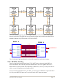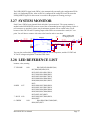
1
Algorithm Acceleration
Logic Emulation
ASIC Verification
User Manual
DNV6F6PCIE
DNV6F6PCIE
User Manual
DOCUMENT PATH
C:\work\dncvs\Boards\DN0200_DNV6F6PCIE\Documents\Manual\DNV6F6PCIE_manual_rev02.docx
LAST SAVED BY
dpalmer on FULLSAIL
LAST SAVE DATE
8/2/2010 12:32:00 PM
Contents
1
INTRODUCTION ............................................................................................................................................. 5
1.1
1.2
1.3
2
QUICK START GUIDE ...................................................................................................................................... 8
2.1
3
STEPS TO FOLLOW .............................................................................................................................................8
HARDWARE ................................................................................................................................................. 15
3.1
3.2
3.3
3.4
3.5
3.6
3.7
3.8
3.9
3.10
3.11
3.12
3.13
3.14
3.15
3.16
3.17
3.18
3.19
3.20
3.21
3.22
3.23
3.24
3.25
3.26
3.27
3.28
3.29
3.30
3.31
4
AUDIENCE........................................................................................................................................................5
CONVENTIONS ..................................................................................................................................................5
RESOURCES ......................................................................................................................................................5
OVERVIEW .....................................................................................................................................................15
VIRTEX 6 FPGA ..............................................................................................................................................16
CLOCK RESOURCES ..........................................................................................................................................18
NMB BUS .....................................................................................................................................................24
FPGA INTERCONNECT......................................................................................................................................26
SODIMM (DDR3) CONNECTORS......................................................................................................................28
DAUGHTER CARDS ......................................................................................................................................31
FPGA CONFIGURATION ..............................................................................................................................45
MARVELL CPU .............................................................................................................................................45
MARVEL TO NMB BRIDGE ................................................................................................................................51
RS232 .........................................................................................................................................................53
GPIO ACCESS HEADER.................................................................................................................................54
USER LEDS ..................................................................................................................................................56
FPGA-TO-FPGA ROCKETIO ...........................................................................................................................56
SPI FLASH ....................................................................................................................................................58
USER TEST POINTS ......................................................................................................................................59
MICTOR CONNECTOR.......................................................................................................................................59
USER SATA ..................................................................................................................................................60
SFP AND ETHERNET ....................................................................................................................................61
ROCKETIO HEADER .....................................................................................................................................63
ENCRYPTION ...............................................................................................................................................65
JTAG ...........................................................................................................................................................67
MECHANICAL ..............................................................................................................................................69
POWER .......................................................................................................................................................70
RESET ..........................................................................................................................................................74
SYSTEM MONITOR ......................................................................................................................................77
LED REFERENCE LIST ...................................................................................................................................77
TEST POINT REFERENCE LIST.......................................................................................................................78
CONNECTOR REFERENCE LIST ....................................................................................................................79
CHARACTARIZATION REPORTS ...................................................................................................................80
UNUSABLE PINS ..........................................................................................................................................81
SOFTWARE .................................................................................................................................................. 82
DNV6F6PCIE User Manual
Page 3
4.1
4.2
4.3
4.4
5
REFERENCE DESIGN ..................................................................................................................................... 95
5.1
5.2
5.3
5.4
6
DIAGRAM ......................................................................................................................................................95
NMB SPACE MAP...........................................................................................................................................95
THINGS TESTED...............................................................................................................................................95
COMPILING ....................................................................................................................................................95
TROUBLESHOOTING .................................................................................................................................... 96
6.1
6.2
6.3
6.4
6.5
6.6
6.7
6.8
6.9
6.10
7
EMU HOST SOFTWARE ......................................................................................................................................82
WRITING YOUR OWN SOFTWARE. .......................................................................................................................87
HOW EMULIB WORKS ......................................................................................................................................87
MARVEL ENVIRONMENT ...................................................................................................................................88
BOARD IS DEAD ............................................................................................................................................... 96
DOES NOT RESPOND OVER PCI EXPRESS ............................................................................................................... 96
MY DESIGN ACTS WEIRD ...................................................................................................................................96
IT WORKS ON ONE FPGA AND NOT OTHERS ..........................................................................................................96
PACEMAKER STOPS WORKING ............................................................................................................................96
SIGNALS LOOKS CRAZY ON SCOPE ........................................................................................................................96
DCM DOES NOT LOCK ......................................................................................................................................96
DESIGN DOESN'T RESPOND OVER NMB ............................................................................................................... 96
FPGAS WILL NOT PROGRAM ............................................................................................................................... 96
DOES NOT BOOT .............................................................................................................................................. 96
ORDERING INFORMATION ........................................................................................................................... 97
7.1
7.2
7.3
7.4
7.5
7.6
PART NUMBER ...............................................................................................................................................97
HOW TO ORDER .............................................................................................................................................97
BOARD OPTIONS .............................................................................................................................................99
COMPATIBLE PRODUCTS ...................................................................................................................................99
WARRANTY ....................................................................................................................................................99
COMPLIANCE INFORMATION..............................................................................................................................99
8
INDEX ........................................................................................................................................................ 101
9
GLOSSARY ................................................................................................................................................. 102
10
REVISION HISTORY .................................................................................................................................... 105
DNV6F6PCIE User Manual
Page 4
1 INTRODUCTION
text
1.1 Audience
This product is marketed and sold to engineers who are familiar with circuit board design, physically
probing AC waveforms, programming FPGAs, wiring HDL code, reading device data sheets,
reading C source code and writing software. The provided support material all assumes that the user
already has these skills.
1.2 Conventions
text here
1.3 Resources
The following list includes the resources that you are expected to make use of.
1.3.1
Website
The product page for this product is on the internet, here:
http://dinigroup.com/index.php?product=DNV6F6PCIe
This page contains:
- Block Diagram of the board
- Marketing Product description
- List supported features
- Latest Errata
- Latest software and firmware update package
- Latest version of this document.
1.3.2
Product Package
The board comes with a USB memory stick with files on it. On the root directory, there is a file
called "Support Package Contents.pdf" that describes the contents and the directory structure.
This package contains the software installed on the board as well as the software that should be
installed on your host computer.
1.3.3
Reference Design
The product package contains a set of FPGA designs written in Verilog HDL that produce working
configurations files for the FPGAs on the DNV6F6PCIE. Project files and batch script files that use
DNV6F6PCIE User Manual
Page 5
ISE to build the designs are also provided. These example files can be use to quickly create working
.bit files for the FPGS.
The reference design implements every feature on the board, including DDR3 memory, RocketI/O,
and others. You are free to adopt any of the device controllers used in this reference design.
For most customers, the most interesting part of the reference design will probably be the UCF file,
which contains a list of all the usable signals connected to the FPGA and the correct IOSTANDARD
attribute to use with each.
1.3.4
Schematics and Netlist
This user manual fails to list specifications for all of the devices connected to the FPGAs, and so to
correctly use them, you will have to refer to the device datasheet and the schematic. The schematic is
provided in PDF format. If you need a machine-readable format, you can use the provided ASCII
netlist of the board. The ASCII netlist contains only nets on the DNV6F6PCIE that are connected to
usable I/O on the FPGA.
1.3.5
Device Datasheet Library
There is a PDF datasheet provided for every part used on the board. It is in the user support package.
1.3.6
Xilinx
Questions about the use of Virtex 6 FPGAs or ISE that aren't specific to the DNV6F6PCIE should be
directed to Xilinx.
1.3.7
Board Models
1.3.8
EMAIL AND Telephone Technical support
Phone support is available pacific standard time from 9AM to 5PM from Monday through Friday,
excluding USA federal holidays. Support is available in English. Support for boards purchased
through distributors can additionally be provided by the distributor. Distributors are listed in the
ordering information section.
Telephone (USA): 858-454-3419
Formal technical support
[email protected]
Expertise
Schematic
Verilog
Sales
Production
Quantum Physics
Host Software
Marvell Software
Name
David Palmer
Jack Fan
Mike Dini
Dela "tats" Cruz
Ivan Yulaev
Neal Harder
David Palmer
DNV6F6PCIE User Manual
Email
[email protected]
[email protected]
[email protected]
[email protected]
[email protected]
[email protected]
[email protected]
Ext.
30
22
11
15
12
28
30
WoW Class (Level)
Jester (30)
Rogue (14)
Barbarian (8)
Sorceress (44)
Wizard (19)
Paladin (21)
Jester (30)
Page 6
1.4 Errata
The circuit board is currently in revision number: 02
Errata exists for revision 01 of the circuit board.
Issue: IDE connector doesn't physically fit on the "ACCESS A" header.
Solution: You must cut the key off your cable connector.
Issue: Real Time clock does not keep time between power-down cycles.
Solution: None.
Issue: Board may not power on immediately after powering off. When this condition occurs, the
board will remain in a "reset" condition, and will be unusable.
Solution: You may need to wait up to 5 seconds after powering down the board before it can be
powered on again.
DNV6F6PCIE User Manual
Page 7
2 Quick Start Guide
This section will walk through an example session using the board.
2.1 Steps to Follow
Follow them.
2.1.1
Examine Contents of Box
The box containing the product should have come with the following units:
DNV6F6PCIE board
RS232 serial Cable
DB9-to-IDC cable adapter
Two PCI Express power cable adapters
USB Stick containing user support package
DNV6F6PCIE User Manual
Page 8
USB Stick containing FPGA .bit files and a shell script.
PSU "starter" device
2.1.2
Before you power on
Place the board on a clear desk with static control padding. You can use the silver-colored bag the
board comes wrapped in as a static control surface. Make sure you neutralize the static in your
fingers with the surface before every time you contact the board.
2.1.3
Install the board in a PCI Express slot
This step is optional. During the course of your project, if you intend to control the board using PCI
Express, then you should complete this step.
The board fits into any 4x, 8x or 16x PCI Express slot. Make sure the computer is powered off when
you install the board into it. It is recommended that you have the computer laying down so that the
DNV6F6 is oriented vertically to reduce physical stresses on the board.
2.1.4
Connect Ethernet Cable
This step is optional. During the course of your project, if you intend to use Ethernet to control the
board, then you should complete this section.
Have a computer network. In order to be able to access the board over the network, the network must
support DHCP. Otherwise, the board will fail to have a usable IP address. Connect the RJ45
connector on the DNV6F6 to your network.
2.1.5
Connect USB Cable
This step is optional. During the course of your project, if you intend to control the board directly
from a computer over USB, then you should complete this step.
Connect a USB cable from the host computer to the "USB type B" connector on the board. If the
board is plugged into PCI Express, the computer that connects to the board with USB does not
necessarily need to be the same computer.
2.1.6
Connect power cables
You need a computer power supply to supply power to the DNV6F6. If the DNV6F6 is installed
inside a computer in a PCI Express slot, then you can use the power supply that powers the rest of
the computer system. Alternately, the power supply can be sitting on a desktop.
The board requires two "PCI Express" Power cables to be plugged in to operate. If you only use a
single cable, the board will fail to power up properly. Most modern computer power supplies have at
least two PCI Express power cables. If your power supply does not, you can use the provided adapter
cables that plug into the "hard drive" power cables.
DNV6F6PCIE User Manual
Page 9
When the board is plugged into a PCI Express slot, the two "PCI Express" power connectors are still
required. If you power on the computer without the power connected to the board, then the board
will not be accessible over PCI Express
2.1.7
Power on the board
Turn on the power supply. If the power supply is sitting on a desktop, then the power supply will not
turn on without a "PSU starter" device. One has been provided for you.
The board has a self-boot process that takes approximately one minute.
2.1.8
Using a USB pen drive to brutally control the board
The board is provided with a USB pen drive that has on it a Linux shell script. If you plug the USB
stick into the board, then the board will automatically run the shell script. The shell script on the
provided pen drive will cause the FPGAs to load with the reference design .bit files. You can tell that
the .bit files are loading because after each FPGA configures, a blue LED will appear on the board.
2.1.9
Host Software
Whether the board is connected to a computer using USB, PCI Express or Ethernet, the board is
controlled using a program that Dini Group has provided called "Emu". The Emu program is
provided in source and as binaries on the user support package.
The rest of this guide will assume you are using a Windows computer, however you can also use
Linux. If you are using Linux the instructions may be slightly different.
If you are using PCI Express then you need to install a PCI Express driver. This can be done in
Windows using the "device manager". The driver files are provided in the support package
D:\Host_controller_software\emu\drivers\pci_win32. Search the internet if you are unsure how to
install a driver from device manager.
If you are using USB then you will need to install a USB driver. This can be done in Windows using
the "device manager". The driver files are provided in the support package
D:\Host_controller_software\emu\drivers\usb_win32. Search the internet if you are unsure how to
install a driver from the device manager.
Ethernet does not require a driver.
2.1.10 Selecting a board
Run the provided "emu" program, located in the user support package here:
D:/Host_software_applications/Emu/App/Bin/Emu_gui_win32.exe
This window will appear.
DNV6F6PCIE User Manual
Page 10
From the "Board" menu, chose "select board". If you are connected to the board over PCI Express,
USB and Ethernet simultaneously, then there will be three options in the pull-down menu. Each
interface is treated like a separate board. From the pull-down menu, you can see the serial number of
each board. The serial number in this menu should match the serial number located on a sticker near
DIMM D of your board.
Once you have selected a board, your window should look like this.
DNV6F6PCIE User Manual
Page 11
2.1.11 Configure an FPGA
You can configure and FPGA by clicking on the image of it in EMU and selecting "configure" from
the pop-up window. There are some example .bit files that you can use in the support package
located at
D:\FPGA_reference_designs\bitfiles\
Be sure to choose bit files that are compiled for the correct type of FPGA that you have installed on
the board, to avoid humiliation and ridicule.
After the FPGA successfully configures, a blue dot will appear next to any configured FPGA.
DNV6F6PCIE User Manual
Page 12
2.1.12 Setting board controls and options
The primary board settings that you will need to modify are the clock settings. There are six clocks
on the board that have modifiable options. Let's change the clock frequency of G0 for kicks.
In the EMU window, click on the right side where the says "CLOCKS: G0". A pop-up menu will
allow you to change the frequency of clock G0. You can also change the frequency using the
"Clocks/Temps" menu in the menu bar. The clock frequency of the six main clocks is constantly
measured and displayed on the screen for your intense pleasure.
2.1.13 Hardware Verification Test
To run the hardware test, from the "Test" menu, select "selected tests".
The tests that you can run now are the temperature test, clock test, blockram test, intercon test, lvds
test and flash test. Let's skip the DRAM test and the "factory tests" for now. After you hit the "OK"
button, the program will ask you to locate the "bit file directory". This is where the test FPGA load
files are stored. There is a "bit file directory" on the provided user support package in
D:\FPGA_Reference_designs\bitfiles
DNV6F6PCIE User Manual
Page 13
Once the test runs, the Emu window will indecisively print "PASS" or "FAIL"
DNV6F6PCIE User Manual
Page 14
3 Hardware
This section, more than any other, describes the board hardware.
3.1 Overview
Below is a block diagram of the board.
Above is a block diagram of the board.
The board contains six Xilinx Virtex-6 FPGAs in the "FF1759" package. There are 5 different Xilinx
part numbers that come in this package. All 5 of these are compatible with this board. The board can
come with any number from 1 to 6 of FPGAs installed, leaving the unused chip positions vacant.
The Virtex 5 "Config FPGA" is not intended for your use, so you should think of it as more of a
"NMB master controller/ bus switch"
Interconnect between the FPGAs is fixed, and routed in a point-to-point fashion. The interconnect is
represented in the block diagram as arrows between the FPGAs. All of the interconnect is userdefined. Notice that some of the interconnect on the board is colored gold instead of black. The
yellow interconnect is only available for use if both of the two FPGAs to which it connects is a
"large package" FPGA, namely LX550T or SX475T.
To connect to other systems, or off-board I/O, there are three "daughtercard" connectors provided. In
the block diagram these appear as yellow rectangles unless you are colorblind then they are grey.
DNV6F6PCIE User Manual
Page 15
The user is expected to buy a daughter card that contains the I/O interface that is required, or to
design their own.
Four DDR3 sockets (red rectangles) are on the board to provide bulk memory for use in the FPGA.
You can use standard, off-the-shelf laptop memory (SODIMM), or you can use one of the many
memory technology DIMMs that the Dini Group provides.
Getting data on and off the board is accomplished through the Marvell CPU. It provides USB,
Ethernet, PCI Express, interfaces. It connected to the user FPGAs through the "NMB" interface,
which is fast enough to sustain a full-speed x4 PCI Express connection to all FPGAs simultaneously.
The interface inside the FPGA and on the host PC is very simple, because all of the software and
hardware between has already been designed, proven, and optimized.
3.2 Virtex 6 FPGA
Virtex 6 is the most slightly better than Virtex 5 FPGA in the world. You will definitely want six of
them.
3.2.1
Stuffing Options
Each of the six main FPGA locations can be installed with any compatible density of FPGA, or not
installed at all, in any combination. In this way, you only will have to pay the (significant) FPGA
cost for the FPGAs that you will actually use.
Below there is a table that describes the major differences between the available FPGAs. Only
FPGAs that Xilinx sells in the "FF1159" package are compatible with this board.
FPGA
Speed
Flip-flops
Equivalent All Board
25x18
Memory
Grades
ASIC Gates Features? multipliers
(bits)
1L, 1, 2
687,360
4.0M
Y
864
22.8M
LX550T
1L, 1, 2, 3
455,040
2.6M
N
576
15.0M
LX360T
1L, 1, 2, 3
301,440
1.7M
N
768
15.0M
LX240T
1L, 1l, 2
595,200
3.4M
Y
2016
38.3M
SX475T
1L, 1, 2, 3
394,000
2.3M
N
1344
25.3M
SX315T
Each LX550T FPGA can emulate approximately 4 million ASIC gates reasonably, however I just
made this number up. It is strongly recommended that you synthesize your actual ASIC design,
mapping to FPGA technology to get an accurate FPGA utilization estimate.
3.2.2
Speed Grades
Xilinx FPGAs usually come in three speed grades. There is no rule of thumb to estimate which speed
grade you will need to run your design at your target frequency. You will only know this once you
have run a synthesis, with FPGA place-and-route, targeting the actual FPGA device skew that you
will be using.
DNV6F6PCIE User Manual
Page 16
3.2.3
Upgrades
If you would like to install only some FPGAs when you order the board, and later add FPGAs or
upgrade FPGAs to larger parts, this is possible; however you should request this before ordering the
board.
3.2.4
Small FPGAs
When one or more of the FPGA locations is populated with a LX360T, LX240T, or SX315T, the
some features of the board become unavailable. This is because these three FPGAs have fewer I/O
than physically exist on the 1759-pin BGA package. The on-board devices that the unused physical
package pins are connected to cannot be used if the populated FPGA is one of these "small" FPGAs.
On the product block diagram, signals that may be unusable due to "small" FPGAs are colored
orange. Below there is a copy of the block diagram, with all orange signals removed. The block
diagram below represents the features available on a board, even if "small" FPGAs are selected.
3.2.5
Safe Handling of FPGAs
There are three easy ways to break the FPGAs.
1) Static electricity
Make sure you keep the board on a static controlled surface, and that you neutralize your body with
that surface before handling the board. Especially sensitive are the FPGA I/Os. These are exposed on
the daughter card headers and also everywhere else.
2) High Voltage
The FPGA I/O can only withstand voltages below and up to the VCCO power supply. When
interfacing the board to some external I/O, make sure your I/O signals are driven at levels that do not
exceed VCCO. If you do not know what VCCO is, then you probably should not be interfacing the
DNV6F6PCIE User Manual
Page 17
board to some external I/O. Note that the maximum allowable VCCO on Virtex 6 is 2.5V. If you are
interfacing with a 3.3V device, then you automatically lose.
3) Board warp
If the board undergoes mechanical stress, the FPGA pins (balls) can separate from the PCB and
result in non-connected signals. The only way I have seen people doing this is by installing and
removing connectors. Make sure that when installing a connector, you are supporting the connector
from the opposite side, so that board warp does not absorb the force of the insertion.
3.3 Clock Resources
The board provides clocks. Clocks are one of the features that board provides. There are clocks on
the board. You can use the clocks that are on the DNV6F6 for clocking.
3.3.1
Clock pins on the FPGA
The Virtex 6 has many fewer "global clock" (GC) pins that previous generations. Instead there are
"Clock Capable" (CC) pins that have restrictions on how they are used. Only some of the "global
clock" networks on the DNV6F6 are connected to "GC" pins on the FPGA. The rest are connected
on "clock capable" pins. A "clock capable" pin might be a MRCC ("multiple region clock capable")
or SRCC ("single-region clock capable"). You will have to consult a datasheet to tell the difference.
The use of each type of pin, MRCC, SRCC, GC result in different effects on timing.
Also, banks 10-18 have different timing than banks 20-38. All "global clock" pins on the DNV6F6
are connected to banks 20-38.
It would be difficult and misleading if I tried to explain how clocks worked internally in a Virtex 6,
so you will need to consult the data book. We tried to connect them to make them as useful and
flexible as possible.
3.3.2
Global Networks
The "global clocks" are the clocks that are provided to all 6 FPGAs, with low skew between the
arrival of the clock pulses at each FPGA. There are 6 such networks. USER_R, USER_L, G0, G1,
G2, and CLK_25
DNV6F6PCIE User Manual
Page 18
Each of them is suitable for synchronous communication between FPGAs.
3.3.3
Clocks G0, G1, G2
The clocks G0, G1 and G2 are from a synthesizer that can produce any frequency from 2KHz to
700MHz with a 50ppm tolerance or better.
DNV6F6PCIE User Manual
Page 19
The synthesizer used is a high-performance, low jitter, high-precision clock generator chip, the
Si5326. To change the clock frequency you can use the EMU software.
The clocks G0, G1 and G2 can also be set to come from the config FPGA. The config FPGA in turn,
can be set to source this clock from the FPGAs. In this way, FPGAs can drive the frequency onto the
global clock networks. This can be useful for controlled clocks and step-clocks. It can also be useful
when a local clock for an FPGA needs to be delivered to all 6 FPGAs with zero delay.
G0 can be sourced from FPGA A or FPGA D. The signal that the FPGA should drive when this
mode is used is called CLK_TO_SPARTAN_Ap and CLK_TO_SPARTAN_Dp respectively.
G1 can be sources from FPGA B or FPGA E. The signal that the FPGA should drive when this mode
is used is called CLK_TO_SPARTAN_Bp and CLK_TO_SPARTAN_Ep respectively.
G2 can be sourced from FPGA C or FPGA F. The signal that the FPGA should drive when this mode
is used is called CLK_TO_SPARTAN_Cp and CLK_TO_SPARTAN_Fp respectively.
3.3.4
CLK_25
This clock network is fixed at 25Mhz. You cannot change it, try as you might.
Fixed
Frequency
R995
100R
TP57
DNI
U35
16
15
68 CLK_25_SOURCEp
68 CLK_25_SOURCEn
From Spartan
+3.3V
R1018
4.7K
BUF_24_OE
22
17
19
20
18
21
C394 C386 C385
0.1uF 0.1uF 0.1uF
3.3.5
CLK
nCLK
OE
VDD
VDD
VDD
GND
GND
Q0
nQ0
Q1
nQ1
Q2
nQ2
Q3
nQ3
Q4
nQ4
Q5
nQ5
Q6
nQ6
Q7
nQ7
R994
100R
CLK_25_TPp
CLK_25_TPn
14
13
12
11
10
9
8
7
6
5
4
3
2
1
24
23
CLK_25_Ap 60
CLK_25_An 60
CLK_25_Bp 60
CLK_25_Bn 60
CLK_25_Cp 60
CLK_25_Cn 60
CLK_25_Dp 60
CLK_25_Dn 60
CLK_25_Ep 60
CLK_25_En 60
CLK_25_Fp 60
CLK_25_Fn 60
CLK_25_CONFIGp 68
CLK_25_CONFIGn 68
LVDS
To
all
FPGAs
ICS85408
SOP65P640X120-24N
USER_L
This clock has no frequency synthesizer, but can come from a variety of sources.
LVDS
42 CLK_USER_LEFT_OUTAp
42 CLK_USER_LEFT_OUTAn
60 CLK_USER_LEFT_OUTDp
60 CLK_USER_LEFT_OUTDn
44 CLK_USER_LEFT_OUTBp
44 CLK_USER_LEFT_OUTBn
3 CLK_USER_LEFT_SPARTANp
3 CLK_USER_LEFT_SPARTANn
3 CLK_USER_LEFT_MUX_SEL0
3 CLK_USER_LEFT_MUX_SEL1
U26
2
3
4
7
8
9
14
13
12
19
18
17
6
5
10
11
CLK0p
VT0
CLK0n
Q0p
Q0n
16
15
LVDS
LVDS
CLK1p
VT1
CLK1n
R564
100R
CLK
nCLK
+3.3V
BUF_USER_LEFT_OE
+2.5V
22
17
19
20
CLK3p
VT3
CLK3n
18
21
SEL0
SEL1
C127 C139 C128
0.1uF 0.1uF 0.1uF
VDD
VDD
ICS854057/TSSOP20
DNV6F6PCIE User Manual
16
15
R548
4.7K
CLK2p
VT2
CLK2n
GND
GND
LVDS
U25
CLK_USER_LEFTp
CLK_USER_LEFTn
1
20
OE
VDD
VDD
VDD
GND
GND
Q0
nQ0
Q1
nQ1
Q2
nQ2
Q3
nQ3
Q4
nQ4
Q5
nQ5
Q6
nQ6
Q7
nQ7
14
13
12
11
10
9
8
7
6
5
4
3
2
1
24
23
TP15
DNI
R570
100R
CLK_USER_LEFT_TPp
CLK_USER_LEFT_TPn
CLK_USER_LEFT_Ap
CLK_USER_LEFT_An
CLK_USER_LEFT_Bp
CLK_USER_LEFT_Bn
CLK_USER_LEFT_Cp
CLK_USER_LEFT_Cn
CLK_USER_LEFT_Dp
CLK_USER_LEFT_Dn
CLK_USER_LEFT_Ep
CLK_USER_LEFT_En
CLK_USER_LEFT_Fp
CLK_USER_LEFT_Fn
CLK_USER_LEFT_Qp
CLK_USER_LEFT_Qn
9
9
44
44
45
45
42
42
47
47
45
45
68
68
To
all
FPGAs
ICS85408
SOP65P640X120-24N
C145
0.1uF
Page 20
The following list are the available sources for the clock USER_L
FPGA A SRC
The FPGA A should drive the signal
CLK_USER_LEFT_OUTAp/n differentially
The FPGA B should drive the signal
CLK_USER_LEFT_OUTBp/n differentially
The FPGA D should drive the signal
CLK_USER_LEFT_OUTDp/n differentially
The user should supply a clock single-ended into the SMA P36,
located on the bottom right of the board. Voltages up to +2.5V
are acceptable.
The clock will be the same frequency as the "MGT" clock. This
has a dubious and unknown use.
FPGA B SRC
FPGA D SRC
SMA
MGT
3.3.6
USER_R
These come from a USER FPGA. They are used for generating a frequency from an FPGA and then
using that new frequency across the board. This is just like USER_L, except there are different
choices for the inputs.
Clock MUXes
LVDS
+2.5V R456
4.7K
60 CLK_USER_RIGHT_OUTCp
60 CLK_USER_RIGHT_OUTCn
R494
4.7K
CONN_SMA
LIGHTHORSE_SASF546-P26-X1
J5
3
2
3
2
60 CLK_USER_RIGHT_OUTEn
4
1
5
CONN_SMA
LIGHTHORSE_SASF546-P26-X1
J6
60 CLK_USER_RIGHT_OUTEp
45 CLK_USER_RIGHT_OUTFp
C702
4
1
5
1uF
45 CLK_USER_RIGHT_OUTFn
CLK_SMA_USER_LEFTp
CLK_SMA_USER_LEFTmid
CLK_SMA_USER_LEFTn
3 CLK_USER_RIGHT_MUX_SEL0
3 CLK_USER_RIGHT_MUX_SEL1
LVDS
U23
2
3
4
7
8
9
14
13
12
19
18
17
6
5
10
11
CLK0p
VT0
CLK0n
Q0p
Q0n
LVDS
LVDS
R523
100R
16
15
CLK
nCLK
+3.3V
CLK1p
VT1
CLK1n
R533
4.7K
BUF_USER_RIGHT_OE
CLK2p
VT2
CLK2n
+2.5V
22
17
19
20
CLK3p
VT3
CLK3n
18
21
SEL0
SEL1
GND
GND
TP12
DNI
R511
100R
U24
CLK_USER_RIGHTp
CLK_USER_RIGHTn
16
15
C105 C99 C103
0.1uF 0.1uF 0.1uF
VDD
VDD
1
20
OE
VDD
VDD
VDD
GND
GND
Q0
nQ0
Q1
nQ1
Q2
nQ2
Q3
nQ3
Q4
nQ4
Q5
nQ5
Q6
nQ6
Q7
nQ7
14
13
12
11
10
9
8
7
6
5
4
3
2
1
24
23
CLK_USER_RIGHT_TPp
CLK_USER_RIGHT_TPn
CLK_USER_RIGHT_Ap
CLK_USER_RIGHT_An
CLK_USER_RIGHT_Bp
CLK_USER_RIGHT_Bn
CLK_USER_RIGHT_Cp
CLK_USER_RIGHT_Cn
CLK_USER_RIGHT_Dp
CLK_USER_RIGHT_Dn
CLK_USER_RIGHT_Ep
CLK_USER_RIGHT_En
CLK_USER_RIGHT_Fp
CLK_USER_RIGHT_Fn
CLK_USER_RIGHT_Qp
CLK_USER_RIGHT_Qn
9
9
44
44
45
45
42
42
47
47
45
45
68
68
ICS85408
SOP65P640X120-24N
C91
0.1uF
ICS854057/TSSOP20
FPGA C SRC
FPGA E SRC
FPGA F SRC
SMA
The FPGA C should drive the signal CLK_USER_LEFT_OUTCp/n
differentially
The FPGA E should drive the signal CLK_USER_LEFT_OUTEp/n
differentially
The FPGA F should drive the signal CLK_USER_LEFT_OUTFp/n
differentially
The user should supply a clock single-ended or differential into the
SMAs J5 and/or J6, located near the top left corner of the board.
Voltage levels up to +2.5V are acceptable.
DNV6F6PCIE User Manual
Page 21
To
all
FPGAs
3.3.7
Frequency-only networks
Frequency only networks are networks that are provided to all six FPGAs, but do not guarantee lowskew between the inputs to the FPGAs. These networks should not be used for fully-synchronous
communication between FPGAs, at least not without phase-adjustment.
3.3.7.1 MGT
The MGT clock network delivers a very low-jitter, high-precision frequency source to the MGT
(GTP, GTX, HTX) tiles of all six FPGAs. This clock is intended to be used only for the RocketIO
interconnect between FPGAs, however the clock is accessible for other types of logic inside the
FPGA.
The MGT network can be driven at one of four different frequencies. You can select the desired
frequency from EMU. Additionally, you can run the MGT network at the same frequency as global
clock G0. This will allow you to select any frequency that exists in the world.
3.3.7.2 CCLK
The "CCLK" pin on the FPGA, or the configuration clock, is used by the config FPGA to send
configuration bitstreams to the FPGA over the selectmap bus. It is not a free-running clock, but has a
minimum period of 20ns. It can be used in the FPGA in conjunction with the STARTUP_V6
primitive. This clock is not configurable.
DNV6F6PCIE User Manual
Page 22
3.3.8
Local Networks
Local networks are networks that are only delivered to a single FPGA.
3.3.9
CLK_TO_*
Some FPGAs have signals that connect from on FPGA to another FPGA's global clock input pin.
These signals are single ended and are called "clk_to_*" where * is either A, B, C, D, E or F. These
can be used for forward a clock from one FPGA to another, without having to use "local routing"
within the FPGA. The utility of this does not exceed 3 utils.
3.3.10 Spartan/TP
There is a test point connected to at least on clock input of each FPGA. There is no known use.
3.3.11 Daughtercard Feedback
Each FPGA that has a daughter card connector also has a signal that loops back from an FPGA
output to a clock input of that same FPGA. The routing length of this signal is the same as the
routing length of the I/O signals to the daughter card. The purpose of this is so that it is possible to
have a clock in the FPGA that is phase-aligned to a clock arriving at the daughter card. The signal is
called "DC*_FEEDBACK_P/N"
3.3.12 DIMM Feedback
Similarly, each FPGA that has a DIMM interface has a signal that is looped back from an output of
the FPGA to a clock input of the FPGA. The routing length of this feedback is equal to the routing
length of the signals to the DIMM connector. In this way, it is possible to have a clock inside the
FPGA that is phase aligned with the arrival of the clock at the DIMM. The signal is called
"DIMM*_FB_P/N"
DNV6F6PCIE User Manual
Page 23
3.3.13 From SEAM connector
The SEAM daughter card provides four clock inputs delivered to the MGT (GTP, GTX, HTX) tiles
of the connected FPGA. This clock is intended to be used for RocketIO communication with the
SEAM interface, however it can be used in the FPGA for other types of logic.
3.3.14 NMB
The NMB interface includes one clock signal running at xxxxxx MHz. This clock is free-running,
and is not configurable. It is received by each FPGA at the same frequency, however the phase
relationship between the arrival of the clock at each FPGA is indeterminate.
3.3.15 Generating clocks from FPGAs
Notice how earlier I said that some of the clock networks can be driven from FPGAs? Well that
means you can do all of your frequency generation in an FPGA.
3.3.16 Clocking features not implemented
Four of the networks can be driven from the configuration FPGA. If you need some special feature,
then we could potentially add it. For example, single-step clocks, clocks from FPGA-to-FPGA.
3.4 NMB Bus
The NMB bus is the primary means you will use to get high quantities of data on and off the board.
If you want to use the provided software (EMU) to push data to the board over USB, Ethernet and
PCI Express, then you are required to interface to NMB in your FPGA design.
3.4.1
Protocol
You are expected to know nothing about the protocol of NMB and only interface to it using the
provided HDL interface wrapper in your FPGA on one end, and in the EMU C++ code on the other
end. However, the marketing material constantly makes reference to the inner workings of the
underlying hardware and software, so I feel obligated to sort of describe it a little. This short section
describes the implementation of the interface. I recommend you skip this "protocol" section. It is
useless to know anything here.
DNV6F6PCIE User Manual
Page 24
There is a block diagram of the NMB bus architecture above. It is physically point-to-point from
each FPGA to the configuration FPGA. Each point-to-point connection consists of a 40-pin signal
wire, which are used as 20 LVDS pairs. These pairs are further divided into 10 signals in each
direction, with 1 clock signals, 1 control signal and 8 data signals. The clock frequency of the
interface happens to be 1GHz (500 MHz clock with DDR capture). The theoretical throughput is
therefore 1GB/sec in both directions simultaneously, to all 6 FPGAs simultaneously.
The protocol supports four channels, demand mode, bursts, interrupts, link detection, some FIFO
flags, and maybe some other stuff. The data to/from the FPGA is stored in buffers in the DRAM of
the Marvell processor.
3.4.2
User Interface
An HDL module is provided in the support package around here:
D:/FPGA_Rererence_designs/code/common/nmb/nmb_target_interface.v
There is hopefully a PDF in that directory that gives a much better description of how to actually use
the interface. But more or less the interface provides a simple Address/DataIn/DataOut type
interface. You should think of the interface as a memory space.
On the C++ side of the NMB there are simple functions like
nmb_read(address, buffer, size)
that can be used to view this memory space. The code for this is found in the support package here
D:/Host_software_applications/Emu/EmuLib/dnapi.h
DNV6F6PCIE User Manual
Page 25
Hopefully there is also a PDF there that describes how to use it.
3.4.3
Memory Spaces
You should probably read the PDF describing dnapi.h instead of this document.
D:\Host_Software\emu\Documents\Emu_Manual.pdf
But here it goes: The memory space is 64-bit. Each address represents a single byte, however the
data is required to be read and written in blocks of 32-bit. Addresses supplied to the interface must
be divisible by 4. Therefore, the bottom 2 bits of the address space are stupid.
Additionally, since there are no chip-selects on the NMB bus, it is necessary to pre-allocate address
ranges for devices on the bus. On this board, there are six devices, and the NMB address ranges that
they are able to respond to on the bus are given here:
Target
FPGA A
FPGA B
FPGA C
FPGA D
FPGA E
FPGA F
3.4.4
Starting Address
0x00000000_00000000
0x01000000_00000000
0x02000000_00000000
0x03000000_00000000
0x04000000_00000000
0x05000000_00000000
End Address
0x00FFFFFF_FFFFFFFF
0x01FFFFFF_FFFFFFFF
0x02FFFFFF_FFFFFFFF
0x03FFFFFF_FFFFFFFF
0x04FFFFFF_FFFFFFFF
0x05FFFFFF_FFFFFFFF
Error Conditions
Exist.
3.5 FPGA Interconnect
Most of the I/O on the FPGA are used to connect each FPGA to other FPGAs. Most interconnect is
routed point-to-point between FPGAs, in a nearest neighbor topology. The exact topology is shown
in the diagram below.
DNV6F6PCIE User Manual
Page 26
Note that the interconnect that is drawn in a gold color in the diagram is only available when both
connected FPGAs are either the LX550T device, or the SX475T device. If either FPGA is a "small"
FPGA device, then the signals are not usable. This is because the "small" FPGA devices do not allow
the use of all of the pins of the FPGA as I/O.
3.5.1
I/O protocol
The protocol for the use of the I/O is user defined. The VCCO pin of the FPGA on each bank that is
used for interconnect is +2.5V. This means that LVCMOS25 and LVDS are both reasonable choices
for the IOSTANDARD attribute.
The board features necessary to use terminated standards, such as LVDCI or SSTL are not provided
on the board, and so DCI cannot be used for FPGA-to-FPGA communication. When using LVDS,
you can still use the DIFF_TERM attribute to terminate signals.
Since the "global clocks" on the board are delivered to each FPGA with low skew, any of the
"global clocks" are suitable for use for FPGA interconnect.
3.5.2
High-Speed interconnect
The interconnect between FPGAs are divided into "banks". A single bank on one FPGA always
connected to a single bank on one other FPGA. This pairing up of banks allows the use of some of
the high-speed features of the Virtex 6, such as BUFR clocking, and ISERDES and OSERDES.
Every "bank" of interconnect contains at least one LVDS pair in each direction that goes to a "clock
capable" pin on the FPGA. This pair can be used as a clock to input all of the bits on that bank. The
net name of this pair ends in "_CC" in the schematic.
DNV6F6PCIE User Manual
Page 27
To achieve the highest switching rates on the interconnect banks, you must use the LVDS
IOSTANARD.
3.5.3
Signal net length report
The shortest FPGA-to-FPGA interconnect signals is 40mm long. The longest is 290mm long. This
corresponds to a skew of about 2ns.
Within any single bus, the greatest skew is 75mm. This corresponds to 0.5 ns of skew.
3.6 SODIMM (DDR3) Connectors
For memory expansion, the DNV6F6PCIe has four socket connectors connected to four of the user
FPGAs. The sockets accept standard off-the-shelf DDR3 laptop memory. The interface and reference
design is compatible with any density or organization of memory.
These sockets can also be used for types of memory other than DDR3 DRAM. Dini Group has a
variety of modules that are compatible with the DNV6F6PCIe, including synchronous SRAM and
others.
The SODIMM interface is also potentially usable as an expansion interface for custom daughter
cards.
DNV6F6PCIE User Manual
Page 28
3.6.1
Memory Interface Generator
The provided reference design uses a memory controller that is based on the memory controller that
is produced by the "Memory Interface Generator" (MIG), part of the ISE software. However it has
been modified. The modifications allow the use of dual-rank DIMMs, and also set some parameters
automatically, such are RAS and CAS latencies, and total DIMM density.
Some of the signals that are connected between the SODIMM connector and the FPGA are not used
by MIG. These include the SODIMM "NC" (no connect) pins, the upper two address pins, the
EVENTn pin.
Additionally, the "feedback" clock is not used by MIG, or the DDR3 controller provided by Dini
Group.
If you want to use MIG you should use the HDL files produced by MIG, and use the UCF file
provided by Dini Group, removing the unused signals.
3.6.2
IO Standards
The DIMM interface is voltage-selectable. When using DDR3 memory, it is suggested to use the
1.5V IO voltage. When using this voltage, signals to the SODIMM should be of the IO Standard
SSTL_II_18_DCI or SSTL_II_18_DIFF_DCI. The necessary board features to make SSTL work
properly are provided.
DNV6F6PCIE User Manual
Page 29
The EVENTn pin is also voltage selectable. It will be the same voltage as the rest of the DIMM.
There are some LED signals on the FPGA that are connected to the DIMM bank. The
IOSTANDARD attribute of these signals must be changes to match the voltage of the DIMM.
The IIC signals (SDA and SCL) are fixed at +2.5V and should use a 2.5V standard.
3.6.3
Voltage Selection
Off-the-shelf DDR3 DRAM always uses 1.5V core power and IO signaling levels. If you are using
DRAM, then you would never need to change the voltage output of the DRAM interfaces. However,
when using alternate memory modules from Dini Group, or when designing your own daughter
cards, you may need to supply a different voltage to the SODIMM and to the attached pins of the
FPGA.
+5.0V
R1192
This
resistor is
duplicated
on other
pages
R1193
1K
R1180
DNI
R1191
5,6,7,59 SEQ_DISABLE_VCCO#
Silkscreen:
1.35V
1.5V
1.8V
Install all for 2.5V
1K
U91-1
REG_DIMMA_TRACK
E1
REG_DIMMA_RUN
D1
REG_DIMMA_COMP
G1
0R
R1171
DNI
F1
TRACK
J32
FB
REG_DIMMA_FB
B3
B4
REG_DIMMA_SW0
REG_DIMMA_SW1
RUN/SS
R1146
DNI
COMP
O.D.
PGOOD
SW
SW
LTM4604A/LGA66
59 PWR_FAULTn_DIMMA
G2
1
3
5
7
2
4
6
8
REG_DIMMA_FB135
REG_DIMMA_FB15
REG_DIMMA_FB18
REG_DIMMA_FB25
R1371
R1370
R1369
R1368
30K
13.7K
6.8K
19.1K
TSM-136-01-T-DV
R1136
DNI
R1161
10K_0.1%
1.2V - 10K
2.7V - 2.1K
1.35V - 7.25K
1.5V - 5.76K
1.8V - 4.02K
2.5V - 2.37K
Each SODIMM interface has an isolated regulator that allows you to independently select the
voltage. There is a header next to each SODIMM where you can install jumpers to affect the output
voltage of this regulator. To change the voltage, remove all jumpers currently installed on the header,
and install a jumper next to the silkscreen text showing that voltage that you want. Be sure to probe
the DIMM_VDD test point once you have completed the change.
DNV6F6PCIE User Manual
Page 30
3.6.4
Daughter cards
If you want to make your own custom daughter card for use in the SODIMM sockets, you are
encouraged to download the complete schematic and layout files for one of our existing custom
modules. These are available on our website with no restrictions on use.
The signals on the DNV6F6PCIE circuit board are routes as 50-ohm impedance. Every signal
connecting to the DIMM is length-matched, including the feedback clock.
Check this webpage to see existing DIMMs and to access the schematic and layout files for existing
DIMMs.
http://dinigroup.com/index.php?page=DNSODM204
3.6.5
Net Length Report
The length of all signals from the FPGA to the SODIMM are length and delay-matched.
3.7 Daughter Card Connectors
The primary means of interfacing to the FPGA with external IO are through the 400-pin MEG-Array
expansion connectors. There are three of these high-speed, high-density connectors on the board,
DNV6F6PCIE User Manual
Page 31
connected to FPGAs D,E and F. The FPGA connection to each of the three connectors is the same.
The physical layout requirements of each of the three connectors is the same.
They are located on the back side of the board in order to leave plenty of flexibility for the
mechanical layout of the board.
DNV6F6PCIE User Manual
Page 32
3.7.1
Electrical Spec
P12-1
PLUG
60 DCD_CLK_DN_IN_P
60 DCD_CLK_DN_IN_N
42 DCD_CLK_UP_OUT_P
42 DCD_CLK_UP_OUT_N
E1
F1
E3
F3
CLK_DN_2.5_P
CLK_DN_2.5_N
+12V
+12V
CLK_UP_2.5_P
CLK_UP_2.5_N
RSVD_PWR
RSVD_PWR
+3.3V
+3.3V
+2.5V_LDO
DCDCO_CAP
C59
1uF
K20
VCCO_CAP
RSTn_3.3_TOLERANT
A1
K1
DCDVFUSED
C1
H1
DCDSVD
B2
D2
G2
DCD3VFUSED
J2
R5
DNI
RESC1005N
F3
5A
FUSE_0429
+12V_R
F6
5A
FUSE_0429
+3.3V
DAUGHTERCARD_RESET_POWER 36,39
DAUGHTERCARD_RESETn 36,39
PLUG
MEG_400_Plug_Stratix3_30
3.7.2
IO Electrical
The part number of the connector part installed on the DNV6F6 is "84520102LF" from FCI. It is
intended that the part number that will be used to connector to this board is the FCI 74390-101 part.
The part 84520102LF is called the "plug" and the 74390-101 is called the "receptacle"
The DNV6F6 is the "host" side of the interface. The mating card is called the "daughtercard"
All signals from the FPGA to the connector are length matched to each other with a minimum
tolerance of 50ps on all Dini Group host boards. All Dini host boards route the FPGA I/O signals as
50-ohm transmission lines.
It is recommended that daughter cards provide a bypass capacitor between the pins B0_VCC0,
B1_VCC0, B2_VCC0, B3_VCC0, B4_VCC0 and ground close to the connector pin on the daughter
card.
Note that Virtex 6 is incompatible with +3.3V I/O signaling completely. +2.5V is the maximum
supported I/O voltage. If you require +3.3V I/O, you must use voltage translation devices.
3.7.2.1 _V pins
Any pin name that ends in the string "_V" is a "VREF" pin.
DNV6F6PCIE User Manual
Page 33
For some settings of the FPGA I/O attribute IOSTANDARD, you are required to supply a 1/2 VCCO
voltage onto the "VREF" pins of the FPGA. If a daughtercard requires one of these IOSTANDARD
settings, it must generate the VREF voltage, and drive it back on the _V pins of the daughtercard.
There are no-stuff capacitor locations on the host board attached to all "VREF" pins that can be
populated with capacitors, if this is required by your electrical analysis. Note that installing these
capacitors will negatively impact the switching speed of these signals when used as regular I/O.
3.7.2.2 _CC pins
Any pin whose name ends in "_CC" is a "CC" pin.
CC pins and _MRCC pins are connected to "CC" pins or "MRCC" pins on the host board's FPGA.
You should see the Virtex 6 SelectIO user guide for the implications of this. But in general, these
pins are suitable for I/O clocks driven from the daughtercard to the host FPGA.
The "CC" pins are able clock I/O in other FPGA banks in some cases. For this capability, there are
requirements that the banks have certain physical relationships to each other on the silicon die of the
FPGA device. During the assignment of FPGA banks to the daughtercard, no provisions were made
to restrict the bank selection to make cross-bank clocking consistent from one daughtercard header to
the next. It is recommended that is CC pins are required, that a separate copy of the clock is driven to
each FPGA bank that requires it, and do not rely on "multi-clock" regions.
3.7.2.3 VRP and VRN Pins
On all FPGA banks that are connected to the daughtercard, VRP and VRN pins are correctly
connected to allow DCI to be used with the daughtercard. Note that there is still the Virtex 6 I/O rule
that only a single type of DCI may be used per bank of the FPGA. This requirement may limit the
use of DCI on the daughter card. The requirement is too complicated to describe here, so you may
need to run a test place-and-route of your design to determine whether your desired pin out is
acceptable.
3.7.3
Reset Signal
The signal RSTn_3.3V_TOLERANT is valid when +2.5V_LDO is above 0.7V. At all times, when
the signal RSTn_3.3V_TOLERANT is valid, and has a voltage measuring below 0.7V, then all
boards using this interface (host and daughtercard) must tri-state all I/O signals connected to the
interface. Daughter cards that fail to tri-state signals until the de-assertion of
RSTn_3.3V_TOLERANT may risk damaging the DNV6F6 board. The DNV6F6 will weakly pull up
this signal to +2.5V. A daughter card is free to also pull up this signal weakly to any voltage between
0.7V and 3.3V
DNV6F6PCIE User Manual
Page 34
+2.5V
+2.5V
TP2
DNI
TESTPOINT
R4
2.0K_0.1%
R6
DNI
U6
MON_DC_ADJ1
MON_DC_ADJ2
1
2
ADJ1
ADJ2
VCC
RST
R3
1K
R7
1K
R2
DNI
3
8
MON_DC_SEL
TMR
REF
SEL
GND
6
5
DAUGHTERCARD_RESETn 36,39
MON_DC_TMR
7
C2
DNI
R347
10K_0.1%
4
LTC2909
C4
0.1uF
+12V_R
R1
1K
RESC1005N
DC Linear Power Supply 2.5V @ 1mA
Current
Limits to
20mA
U22
REG_DC_RESET_IN
8
5
C614
4.7uF_12V
C6
0.1uF
3
6
7
IN
D1
OUT
SHDN SENSE/ADJ
GND
GND
GND
NC
1
DAUGHTERCARD_RESET_POWERq
2
REG_DC_RESET_ADJ
1
2
DAUGHTERCARD_RESET_POWER 36,39
DIO_DFLS130L-7
4
LT1963AES8/SO8
R353
6.8K
C3
4.7uF
C5
0.1uF
R372
6.04K
Requires a GND area fill for thermal
performance, reference the
datasheet.
3.7.4
Power
The DNV6F6 supplies power to the daughtercard at two voltages, 12V and 3.3V. Each pin of the
Meg connector can supply no more than 1A of current, so the effective power limit of the
daughtercard is 2A x 12V + 3A x 3.3V = 33.9W.
It is strongly recommended that daughter cards provide a means of isolating (series resistor) their
power net with the host board, and provide a means of bypassing the power input with an external
power connector.
On other Dini Group boards, the pins C1 and H1 may be power pins. On the DNV6F6, these pins are
no-connects.
The daughtercard should never be capable of supplying current back onto the host board on the
+12V or +3.3V nets. This could potentially damage the host board.
3.7.5
VCCO Power
The FPGA I/O power pins are connected directly to the meg-array daughtercard interface. The
intention of this design is for the daughtercard to drive the necessary I/O voltage back onto the host
board. There are linear voltage regulators on the DNV6F6 that bias these power rails to 1.2V,
however it is not recommended that you use these to power the daughtercard I/O. These regulators
can supply up to 1A of current.
If you build a daughter card that drives current back to the host board, it must be able to supply the
current not only for the daughter card I/O, but also for the I/O current requirements of the host board.
DNV6F6PCIE User Manual
Page 35
If you forget to include voltage regulators for VCCO on the daughtercard, you can rework the
DNV6F6 bias regulators to output your required voltage, so only as the combined current
requirements of the FPGA banks and the daughtercard do not exceed 1A per bank. Note that the 5
voltage regulators on the host board are not set up to evenly share current loads, and that each must
be individually load limited to 1A.
P3
DCD_B0_VCCO
DCD_B1_VCCO
DCD_B2_VCCO
DCD_B3_VCCO
DCD_B4_VCCO
1
2
3
4
5
6
1
2
3
4
5
6
DNI
HDR6
There is a row of test points next to each daughtercard header allowing the easy probing of the 5
voltage rails on the daughtercard interface.
R367
DNI
+2.5V
U17
8
5
C18
4.7uF
3
6
7
IN
OUT
SHDN SENSE/ADJ
GND
GND
GND
NC
LT1963AES8/SO8
SOIC127P600X175-8N
1
2
DCD_B0_VCCO 31
REG_DCD_ADJ_B0
R397
0R
4
R398
4.7K
Arrogantly
assumes more
capacitance is
on bank
36,39 DAUGHTERCARD_RESETn
This is the bias regulator. There is one for each of the 5 banks on each daughtercard interface.
3.7.6
Clock Pins
The clock pins E1, F1, E3, F3 are always connected to 2.5V I/O on the FPGA. They are connected to
clock input pins near the center of the FPGA, making them suitable for sending a clock from the
daughter card to the host FPGA. They are not externally terminated on the board, but you can use
DIFF_TERM in the FPGA if you are using differential signaling.
In addition to these two clocks, there is a variable-voltage clock input to the host FPGA. This signal,
B0_P1?_GCC_TERM is located on bank 0. The input levels will be determined by the bank 0
voltage, and the IOSTANDARD settings of the I/O in the FPGA. There exists external endtermination resistors on the host board, terminating to a voltage of VCCO/2. This termination
scheme will result in a high current on the signal.
DNV6F6PCIE User Manual
Page 36
FPGA D
Meg-Array Connector
U3-12
H42
J39
K36
L33
M30
T28
VCCO_25
VCCO_25
VCCO_25
VCCO_25
VCCO_25
VCCO_25
IO_L0P_25
IO_L0N_25
IO_L1P_25
IO_L1N_25
IO_L2P_25
IO_L2N_25
IO_L3P_25
IO_L3N_25
IO_L4P_25
IO_L4N_VREF_25
IO_L5P_25
IO_L5N_25
IO_L6P_25
IO_L6N_25
IO_L7P_25
IO_L7N_25
IO_L8P_SRCC_25
IO_L8N_SRCC_25
IO_L9P_MRCC_25
IO_L9N_MRCC_25
IO_L10P_MRCC_25
IO_L10N_MRCC_25
IO_L11P_SRCC_25
IO_L11N_SRCC_25
IO_L12P_25
IO_L12N_25
IO_L13P_25
IO_L13N_25
IO_L14P_25
IO_L14N_VREF_25
IO_L15P_25
IO_L15N_25
IO_L16P_VRN_25
IO_L16N_VRP_25
IO_L17P_25
IO_L17N_25
IO_L18P_GC_25
IO_L18N_GC_25
IO_L19P_GC_25
IO_L19N_GC_25
K33
K32
N28
P28
K35
K34
L31
L32
J37
J36
N29
N30
H39
H38
L35
L36
K38
J38
P27
R27
R28
R29
K37
L37
H40
H41
L34
M34
J40
J41
M33
M32
K39
K40
M31
N31
J42
K42
P30
P31
DCD_B0_P17
DCD_B0_N17
DCD_B0_P9
DCD_B0_N9
DCD_B0_P7
DCD_B0_N7
DCD_B0_P3
DCD_B0_N3
DCD_B0_P2
DCD_B0_N2_VREF
DCD_B0_P11
DCD_B0_N11
DCD_B0_P16
DCD_B0_N16
DCD_B0_P14
DCD_B0_N14
DCD_B0_P15
DCD_B0_N15
P12-2
PLUG
C832
DCD_B0_P4_CC
DCD_B0_N4_CC
DCD_B0_P13_CC
DCD_B0_N13_CC
DCD_B0_P6
DCD_B0_N6
DCD_B0_P5
DCD_B0_N5
DCD_B0_P1
DCD_B0_N1_VREF
C765
DCD_B0_P10
DCD_B0_N10
DCD_B0_VRN
R477
DCD_B0_VRP
R476
DCD_B0_P12
DCD_B0_N12
DCD_B0_P8_GCC_BUS
DCD_B0_N8_GCC_BUS
DCD_B0_P0_GCC_DN
DCD_B0_N0_GCC_DN
DCD_B0_P0_GCC_DN
A3
DCD_B0_N0_GCC_DN
B4
DCD_B0_P1
A5
DCD_B0_N1_VREF
B6
DCD_B0_P2
A7
DCD_B0_N2_VREF
B8
DCD_B0_P3
A9
DCD_B0_N3
B10
DCD_B0_P4_CC
A11
DCD_B0_N4_CC
B12
DCD_B0_P5
A13
DCD_B0_N5
B14
DCD_B0_P6
A15
DCD_B0_N6
B16
DCD_B0_P7
A17
DCD_B0_N7
B18
DCD_B0_P8_GCC_BUS E5
DCD_B0_N8_GCC_BUS F5
DCD_B0_P9
H3
DCD_B0_N9
G4
DCD_B0_P10
H5
DCD_B0_N10
G6
DCD_B0_P11
H7
DCD_B0_N11
G8
DCD_B0_P12
H9
DCD_B0_N12
G10
DCD_B0_P13_CC
H11
DCD_B0_N13_CC
G12
DCD_B0_P14
H13
DCD_B0_N14
G14
DCD_B0_P15
H15
DCD_B0_N15
G16
DCD_B0_P16
H17
DCD_B0_N16
G18
DCD_B0_P17
H19
DCD_B0_N17
G20
DNI
DCD_FEEDBACKp 42
DCD_FEEDBACKn 42
DNI
50R
50R
DCD_B0_VCCO 33
XC6VLX240T/550T_FF1759
A6
C846
1uF
C730
4.7uF
C731
4.7uF
C684
4.7uF
C640
4.7uF
DCD_B0_P8_GCC_BUS
DCD_B0_N8_GCC_BUS
DCD_B0_P0_GCC_DN
DCD_B0_N0_GCC_DN
3.7.7
B0_P0_GCC_DN
B0_N0_GCC_DN
B0_P1
B0_N1_VREF
B0_P2
B0_N2_VREF
B0_P3
B0_N3
B0_P4_CC
B0_N4_CC
B0_P5
B0_N5
B0_P6
B0_N6
B0_P7
B0_N7
B0_P8_GCC_BUS
B0_N8_GCC_BUS
B0_P9
B0_N9
B0_P10
B0_N10
B0_P11
B0_N11
B0_P12
B0_N12
B0_P13_CC
B0_N13_CC
B0_P14
B0_N14
B0_P15
B0_N15
B0_P16
B0_N16
B0_P17
B0_N17
C639
4.7uF
R478
R479
R481
R480
R455
R486
R484
R485
C683
4.7uF
C46
1uF
B0_VCCO
PLUG
MEG_400_Plug_Stratix3_30
100R
100R
100R
100R
100R
100R
100R
100R
Net Lengths
All daughtercard signals are matched between 60mm and 80mm. This corresponds to a maximum
signal skew of 180ps, in addition to the skew caused by the FPGA device.
3.7.8
Physical Spec
Daughter cards are mounted on the "back" or "solder" side of the PCB, opposite the FPGAs. This
allows for maximum vertical mechanical flexibility. The vertical clearance of components on the
reverse side of the DNV6F6 is 3mm. The board-to-board clearance between the daughtercard and the
host board is 14mm. Therefore, the daughtercard may have 10mm components on its side facing the
base board, leaving 1mm of clearance.
The "front" or "component" side of the daughtercard is the face that points away from the host board.
Therefore, the "back" or "solder" sides of the host and daughter cards face toward each other.
The position and size of four mounting holes through the DNV6F6 PCB with respect to each
daughtercard interface is fixed. Every Dini Group product with 400-pin MEG interfaces has at least
four mounting holes with this offset.
DNV6F6PCIE User Manual
Page 37
View: Top Side
300-Pin Receptacle on Back
P/N: 84553-101
A1
0.500"
0.500"
0.750"
1.950"
0.750"
A1
0.500"
1.950"
4.250"
View: Top Side
400-Pin Receptacle on Back
P/N: 74390-101
5.000"
Type 0/1/4 Short
4.250"
Type 2 Short
3.250"
2.75"
3.250"
5.000"
2.75"
0.500"
In the above diagram, a daughtercard is designed that has holes matching the position of the holes on
the base board, so that a 14mm, M3 size standoff can be used to stabilize it onto the base board. The
dimensions of the daughtercard above are guaranteed to physically fit onto any Dini Group host
board while that board is installed inside a PC case. Boards larger than the above given dimensions
may not physically fit onto your Dini Group host board. If you cannot fit your daughter card design
in this form factor, then you must examine the physical dimensions of the target host board to
determine the maximum dimensions available.
For a larger vertical clearance between the host and daughter cards, a vertical extender board is
available. The diagram below shows the vertical clearance when used with an extender.
DNV6F6PCIE User Manual
Page 38
3.7.9
Insertion and removal
Due to the small dimensions of the very high speed Meg Array connector system, the pins on the
plug and receptacle of the Meg Array connectors are very delicate.
When plugging in a daughter card, make sure to align the daughter card first before pressing on the
connector. Be absolutely certain that both the small and the large keys at the narrow ends of the Meg
Array line up BEFORE applying pressure to mate the connectors!
Error! Objects cannot be created from editing field codes.
Figure 1 - Daughter card installation step 1
Place it down flat, then press down gently.
Error! Objects cannot be created from editing field codes.
Figure 2 - Install Daughter card step 2
Mating can be started from either end. Locate and match the connector’s A1 position marking
[triangle] for both the Plug and Receptacle. (Markings are located on the long side of the housing.)
Rough alignment is required prior to connector mating as misalignment of >0.8mm could damage
connector contacts. Rough alignment of the connector is achieved through matching the Small
alignment slot of the plug housing with the Small alignment key of the receptacle housing and the
large alignment slot with the large alignment key. Both connector housings have generous lead-in
around the perimeter and will allow the user to blind mate assemble the connectors. Align the two
connectors by feel and when the receptacle keys start into the plug slots, push down on one end and
then move force forward until the receptacle cover flange bottoms on the front face of the plug.
Like mating, a connector pair can be unmated by pulling them straight apart. However, it requires
less effort to un-mate if the force is originated from one of the slot/key ends of the assembly.
(Reverse procedure from mating) Mating or un-mating of the connector by rolling in a direction
perpendicular to alignment slots/keys may cause damage to the terminal contacts and is not
recommended.
DNV6F6PCIE User Manual
Page 39
3.7.10 Clocking Methods
A wide variety of clocking topologies were considered when designing the MEG interface. There
should be at least one clocking method possible that will meet your needs. A list of reasonable
clocking methods are listed and diagramed below.
3.7.10.1 Manual phase alignment
You can use a PLL inside the FPGA to manually align the phase of a clock that you send from the
FPGA to a MEG card.
3.7.10.2 Synchronous with daughter card
You may need to have a clock with edges that arrive simultaneously to the FPGA and to the MEG
daughter card. Each FPGA with a MEG interface has a feedback path that can be used to align a
clock going to the MEG with one going to the FPGA.
This allows a device on operate fully synchronously with the FPGA.
3.7.10.3 Forwarding a global synchronous clock
If you need a device on the MEG card to operate fully synchronously to all FPGAs on the DNV6F6,
then you can use a PLL in the FPGA as shown in the diagram.
DNV6F6PCIE User Manual
Page 40
This circuit will delay a copy of a "global clock" to the MEG card such that the phase will arrive at
the MEG card at the same time that it arrives at all of the FPGAs.
3.7.10.4 Source-Synchronous inputs
Since the signals to the daughter card are length-matched, you can rely on a tight timing relationship
between the clock and data that you send from the daughtercard to the FPGA. Since the FPGA has a
zero-hold-time input, sending a clock from the MEG card whose rising edges are aligned with the
data transitions on your data lines will result in reliable communication with the FPGA.
DNV6F6PCIE User Manual
Page 41
3.7.10.5 Source-synchronous outputs
You can repeat this setup in the opposite direction, as long as the hold time on the device on the
MEG card is zero or negative.
3.7.10.6 Skewed Clocks
The I/O on the FPGA can be used on either rising or falling edges of a clock, so it is easy to invert
the clock on the FPGA device, so that it operates 180 degrees out of phase with the daughter card. Of
you can invert the clock as you output it to the daughter card. The maximum frequency of the
interface when using this method is effectively reduced by half.
DNV6F6PCIE User Manual
Page 42
3.7.11 Incorrect Clocking Methods
The following are methods that don't work.
3.7.11.1 Hold time violation
The following diagram shows a method that potentially violates hold time on the device on the MEG
card.
DNV6F6PCIE User Manual
Page 43
3.7.11.2 PLL cascade
When using PLLs in the FPGA, make sure that there is not another PLL anywhere in the feedback
loop of the PLL or it will result in an unreliable phase output.
3.7.12 Compatibility with older Dini Boards
The "MEG" interface has been included on Dini Group board since 2005 with the Virtex 4 series of
boards, however the features provided by the interface have changed since then. Any daughter card
that meets the following criteria will be compatible with the DNV6F6PCIE:
- Designed for use with a Dini Group Xilinx FPGA board (not Altera)
- Uses only a single voltage for the whole daughter card
- Does not use I/O signal levels above +2.5V
- Uses the "reset" signals as an input only
- Does not require the use of the +5.0V power pin
- Uses no differential signals
All Virtex 6 boards provide the same features on all MEG interfaces, so any daughtercard designed
for use on a Virtex 6 board will work on any MEG connector on any Virtex 6 board that Dini Group
sells.
3.7.13 How to make a daughter card
It is recommended that you start with one of the Dini Group daughter cards as a design template. The
ORCAD schematic, and layout files are all provided on the Dini Group website for several daughter
cards.
DNV6F6PCIE User Manual
Page 44
3.7.13.1 Ensuring backward compatibility
In order to build a daughter card that is compatible with all Dini Group host boards, you should use
the following guidelines:
1) Use the standard 2.75" x 4.25" form factor.
2) Use the same I/O voltage for all I/O pins on the daughter card
3) Supply I/O voltage from the daughter card on all 6 VCCO pins
4) Do not use CC pins
5) Only use differential signaling standards for clocks that drive to the base board
6) Do not use the +5.0V power pin, if one is present.
7) If VREF is needed, it must be driven onto all VREF pins of the entire MEG interface
3.8 FPGA CONFIGURATION
3.8.1
Select map
3.8.2
JTAG
3.9 Marvell CPU
The clock networks, off-board I/O, NMB and configuration is controlled by a Marvell ARM CPU.
This section describes the hardware attached to the Marvell processor. For information about
programming the Marvell and the software running on the Marvell, see the software section of the
manual.
DNV6F6PCIE User Manual
Page 45
The primary purpose of the Marvell processor is to pump data from a host interface (PCI Express,
Gigabit Ethernet, SATA, Flash, or USB) to and from the user's design in the FPGA.
Additionally, these host interfaces can also be used to control the settings of the board's resources,
like clock synthesizers, and configure FPGAs.
The software that comes pre-loaded on the Marvel processor is running the Linux operating system.
For this section, it is assumed that you have a working understanding of Linux.
3.9.1
RS232
The console output of Linux is directed to an RS232 port. In order to connect a terminal to this port,
you will need to set the terminal settings to 19200 baud, 8bit, no parity, no flow control, 1 stop bit.
DNV6F6PCIE User Manual
Page 46
The Linux console is connected to a shell, so you can interact with the system, however the main
purpose of the console is to receive kernel debugging messages, so it is recommended that you
instead use a telnet terminal, as this shell will be much less chatty.
In order to interact with the boot loader, or see output from the boot process, you must use the RS232
console, you cannot use telnet for these purposes.
3.9.2
PCI Express
The Marvell device natively contains a PCI Express device. The PCI express pins of the Marvell
processor are connected directly to the edge connector of the DNV6F6 board.
DNV6F6PCIE User Manual
Page 47
The device appears as three 1MB memory regions to the host machine. You are expected to use the
Emu software to interface with PCI Express. There is no description available of the function of
DNV6F6 as a PCI Express device.
3.9.3
SATA
The Marvell device contains natively two SATA host ports. In the pre-installed software these ports
are managed by Linux, and you are not intended to directly interact with SATA hardware. Instead,
when a device is installed, it is automatically mounted as a storage device with a filesystem.
From that point, you should use Linux scripts and programs to interact with the mounted filesystem.
3.9.4
DEV Bus: NAND
The root file system of the Linux installation is contained on the NAND Flash device connected to
the Marvell's "device bus". The NAND is 256MB in size, with the first 100MB already assigned to
the Linux installation.
3.9.5
DEV Bus: FPGA
The Marvell "device bus" is also attached to the "config FPGA". This connection has no purpose.
3.9.6
USB
The Marvell device natively provides a USB host and peripheral device. The two "host" devices are
managed by Linux. You are not expected to interact directly with the host ports. Instead, when a
device is detected, Linux automatically mounts the devices as storage devices with filesystems. You
should write linux scripts and programs to interact with the mounted filesystems.
DNV6F6PCIE User Manual
Page 48
The single "device" interface is intended to be used as a connection to a host PC that will be used
with the provided "EMU" software. You are expected to use the EMU controller library to interact
with this device.
3.9.7
IIC Bus: Temperature Sensors
The temperature sensors for the user FPGAs, for the Marvell processor and for the config FPGA are
connected to the Marvell's two-wire serial interface. The installed software will poll these IIC
interfaces and measure the temperature of the FPGAs. If the FPGAs are not within a specified
temperature range, the software will automatically clear the overheated FPGA both to alert the user
to the problem, and to prevent damage to the FPGAs.
3.9.8
ICE
There is an interface for running a hardware debugger on the Marvell processor. It is not expected
that anyone will use this interface, and so details are omitted here.
DNV6F6PCIE User Manual
Page 49
3.9.9
SDRAM
The Marvell environment has 1GB of DRAM managed by Linux.
3.9.10 SPI Bus: Flash
The linux kernel and uboot bootloader are contained on a SPI flash device. The marvell boots by
running instructions from address 0x0 of the SPI flash device. There is a 4-pin SPI programming
header attached to this SPI flash. In order to program the flash device, the Marvell must be
continually held in reset to prevent interference with the SPI programming process.
3.9.11 Ethernet
The Marvell Processor natively contains three gigabit Ethernet port. Only one of these three ports are
enabled. The ethernet port is managed by linux. You are expected to use standard Linux
programming APIs to access these ports from the Marvell side of the link, and to write you own
software for the host side of the link. Several ports are used by the provided Emu software, and you
can use the communication framework provided to interact with your board over ethernet.
DNV6F6PCIE User Manual
Page 50
3.9.12 Multi-CPU
The Marvell Processor has two CPUs. The first, CPU0 is used by the Linux operating system. Since
Linux does not support symmetric multi-processing, the second CPU, CPU1 must be operated in unhosted mode, in its own area of DRAM, without accessing devices. I/O must be accomplished
through CPU0 under Linux.
The use of PCI Express and the DMA engine in the configuration FPGA is possible. Interrupts may
also be used by CPU1.
3.10 Config FPGA
The "seventh" FPGA on the board, the config FPGA (FPGA Q) is not really intended for the user. It
is a "cleanup" FPGA that controls all the clock circuits on the board, configures the other FPGAs,
and multiplexed the NMB bus from the Marvell CPU to the user FPGAs. You don't need to know
anything about it or how it works. You are encouraged to skip this section.
3.10.1 PCI Express
The config FPGA is connected to the Marvell processor through a PCI Express interface. The config
FPGA is a PCI Express endpoint, and the Marvell acts as a root port.
3.10.2 Configuring the Config FPGA
The configuration signals of the config FPGA are connected to the Marvell CPU. The Marvell CPU
gets the .bit file for configuring the "config FPGA" off of the NAND flash. The "config FPGA" also
DNV6F6PCIE User Manual
Page 51
has a SPI flash attached to the configuration signals that can be used to store configuration data,
however it is unused.
3.10.3 RS232
The "config" FPGA passes through the user's RS232 signals to the RS232 buffer.
3.10.4 Count Clocks
All of the boards "global clocks" are connected to the config FPGA. The config FPGA measures the
frequency so that software can report it.
3.10.5 JTAG
The config FPGA has a dedicated JTAG chain and connector that can be used with the IMPACT
program from Xilinx. It has no purpose.
3.10.6 Device Bus
The "config FPGA" has a "device bus" interface connected between it and the Marvell CPU. In this
way the CPU can access the config FPGA as a memory-mapped device. This interface serves no
purpose on this board.
3.10.7 Blink LEDs
The config FPGA is connected to 6 green LEDs. It blinks these LEDs incessantly. The LEDs have
no purpose or meaning.
3.10.8 Controlling Clocks
The control signals for the "global clock" synthesizer chips, and the multiplexer chips are conncted
to the config FPGA. Software is able to set these control siganls.
3.10.9 Clock MUX
The config FPGA serves as one stage of multiplexers for the clocking network. On the schematic
you may see that clocks G0, G1 and G2 come from the config FPGA. The config FPGA drives out
clock signals coming from the user FPGAs on the "TO_SPARTAN" wires, depending on software
settings.
3.10.10 Configuring the FPGAs
The configuration FPGA is connected to the "selectmap" configuration bus of the six user FPGAs. It
uses this bus to configure and read back the configuration data of the user FPGAs.
3.10.11 Marvel to NMB Bridge
The NMB interface connects each user FPGA to the config FPGA. The data that goes to and from
the FPGA winds up in the Marvell CPU's DRAM. Since the config FPGA has a PCI Express link to
the Marvell Processor, it is able to directly manipulate memory in the Marvell's DRAM. The config
FPGA has a DMA controller inside of it that pushes data directly from the FPGAs to the Marvell
DRAM.
DNV6F6PCIE User Manual
Page 52
There is a bunch of detail about how to use this DMA controller that you don't need to know
documented in the "PCIE DMA user manual" PDF document. You should not read this document.
3.11 RS232
There is a pair of signals (RX and TX) for RS232 "Serial" communication to the FPGAs.
DNV6F6PCIE User Manual
Page 53
CPU
J31
1
3
5
7
9
2
4
6
8
10
TSM-136-01-T-DV
UART - CPU and CF FPGA (RS232)
+5.0V
U101
RS232_MCU_TX
RS232_CFPGA_TX
63 RS232_MCU_TX
RS232_MCU_RX
RS232_CFPGA_RX
63 RS232_MCU_RX
14
13
16
15
T1IN
T2IN
R1OUT
R2OUT
R1IN
R2IN
VCC
VL
+1.8V_CPU
R247
T1OUT
T2OUT
4.7K
RS232_ON
11
ON/OFF
SW
CAP
8
GND
VDD
VEE
3
4
Configuration FPGA
+12V_R
R1391
DNI
RS232_TXD1
RS232_TXD2
J37
+12V_LCD
R1390
1
2
+5V_LCD
RS232_RXD1
RS232_RXD2
1
3
5
7
9
2
4
6
8
10
DNI
5
12
TSM-136-01-T-DV
+1.8V_CPU
L1
7
RS232_SW
10
RS232_CAP C2290
C2298
RS232_VDD
RS232_VEE
6
9
0.1uF
0.1uF
10uH
C2291
1uF
LTC2804-1/SSOP16
SOP64P601X175-16N_REC
C2304
1uF
C2299
1uF
RS232 is only available to FPGAs A, B and E. If you need access to it from other FPGAs, you will
have to forward signals between FPGAs to accomplish this.
3.12 GPIO ACCESS HEADER
FPGA A has a few connections to a simple, tenth-inch header.
DNV6F6PCIE User Manual
Page 54
This header is perfect for probing. Note that on revision 01 of the circuit board, it is located too close
to the stiffener bar for a standard IDC cable with a key to plug into it. You can either flip the cable
around backward, or cut the key off, or use a welding torch to burn away one millimeter of
aluminum.
J39
ACCESS_PINS_D1
ACCESS_PINS_D3
ACCESS_PINS_D5
ACCESS_PINS_D7
ACCESS_PINS_D9
ACCESS_PINS_D11
ACCESS_PINS_D13
ACCESS_PINS_D15
ACCESS_PINS_D17
ACCESS_PINS_D21
ACCESS_PINS_D23
ACCESS_PINS_D25
ACCESS_PINS_D27
ACCESS_PINS_D29
ACCESS_PINS_D31
ACCESS_PINS_D30
ACCESS_PINS_D24
ACCESS_PINS_D20
ACCESS_PINS_D2
1
3
5
7
9
11
13
15
17
19
21
23
25
27
29
31
33
35
37
39
IO
IO
IO
IO
IO
IO
IO
IO
IO
GND
IO
IO
IO
IO
IO
IO
IO
IO
IO
IO
Single
GND
IO
IO
IO
PAIRS
IO
IO
IO
IO
IO
KEY (GND)
GND
GND
Single
GND
IO
Single
GND
IO
IO
IO
IO
Single
GND
2
4
6
8
10
12
14
16
18
20
22
24
26
28
30
32
34
36
38
40
ACCESS_PINS_D4
ACCESS_PINS_D6
ACCESS_PINS_D8
ACCESS_PINS_D10
ACCESS_PINS_D12
ACCESS_PINS_D14
ACCESS_PINS_D16
ACCESS_PINS_D18
ACCESS_PINS_D28
ACCESS_PINS_D32
ACCESS_PINS_D26
ACCESS_PINS_D22
ACCESS_PINS_D19
TENTH_INCHES
HDR2X20
The signals connect straight to the FPGA I/O pins. Note the signals are fixed at +2.5V. They are not
+3.3V tolerant. If you connect a +3.3V device (like a hard drive) then FPGA A will likely be
destroyed. The pin out is the same as a Ultra ATA cable. The Ultra ATA cable is capable of highspeed, relative to a standard IDC cable. This cable would be ideal to connect two boards to each
other. Recall how I said that connecting a hard drive will damage the FPGA. This is because the
DNV6F6PCIE User Manual
Page 55
voltages driven by the hard drive will exceed +2.5V which is the maximum allowable voltage. The
pin out was selected because the cable is easy to obtain, not because the FPGA is compatible with
ATA.
3.13 USER LEDS
The FPGAs are all connected to LEDs which have the ON and OFF capability. Some of them go
through FETs.
There is not a lot to say about LEDs.
USER DEFINED LEDS
1.8mA
+2.5V
R971
475R
R977
475R
R981
475R
R986
475R
R990
475R
LED_Ar0
LED_Ar1
LED_Ar2
LED_Ar3
LED_Ar4
DS46
Y ELLOW
LED_0603
LED_Aq0
DS47
Y ELLOW
LED_0603
LED_Aq1
DS48
Y ELLOW
LED_0603
LED_Aq2
DS49
Y ELLOW
LED_0603
LED_Aq3
DS50
Y ELLOW
LED_0603
LED_Aq4
Q16
BSS138
3
SOT-23N_GSD
2
1
LED_A0
Q17
BSS138
3
SOT-23N_GSD
2
1
LED_A1
Q18
BSS138
3
SOT-23N_GSD
2
1
LED_A2
Q25
BSS138
3
SOT-23N_GSD
2
1
LED_A3
Q32
BSS138
3
SOT-23N_GSD
2
1
LED_A4
If you pulse a signal to them, then they will be varying levels of brightness. They are sort of yellow
in color. Other yellow items include sunflowers and fire.
3.14 FPGA-to-FPGA ROCKETIO
Most of the "Rocket IO" or "MGT" or "GTP" or "GTX" signals on the FPGA devices just connect to
other FPGAs
DNV6F6PCIE User Manual
Page 56
Here is the connection topology shown in a diagram format. Note how some of the connections are
drawn in a gold color. The signals that are represented in gold are only available when both FPGAs
attached by them are "big" FPGAs, that is LX550T or SX475T.
FPGA A
FPGA B
U0-33
U1-37
MGTTXP0_112
MGTTXN0_112
MGTRXP0_112
MGTRXN0_112
MGTTXP1_112
MGTTXN1_112
AH8
AH7
MGTREFCLK1P_112
MGTREFCLK1N_112
MGTRXP1_112
MGTRXN1_112
MGTTXP2_112
MGTTXN2_112
AK8
AK7
MGTREFCLK0P_112
MGTREFCLK0N_112
MGTRXP2_112
MGTRXN2_112
MGTTXP3_112
MGTTXN3_112
MGTRXP3_112
MGTRXN3_112
AP3
AP4
MGT_ABn0
MGT_ABp0
E6
E5
AN5
AN6
MGT_BAn0
MGT_BAp0
F4
F3
AN1
AN2
MGT_ABn1
MGT_ABp1
F8
F7
AM7
AM8
MGT_BAn1
MGT_BAp1
G2
G1
AM3
AM4
MGT_ABn2
MGT_ABp2
G6
G5
AL5
AL6
MGT_BAn2
MGT_BAp2
H4
H3
AL1
AL2
MGT_ABn3
MGT_ABp3
H8
H7
AJ5
AJ6
MGT_BAn3
MGT_BAp3
J2
J1
XC6VLX240T/550T_FF1759
MGTRXN3_117
MGTRXP3_117
MGTTXN3_117
MGTTXP3_117
MGTRXN2_117
MGTRXP2_117
MGTREFCLK0N_117
MGTREFCLK0P_117
G9
G10
CLK_MGT_INTERCON_B117n 23
CLK_MGT_INTERCON_B117p 23
MGTTXN2_117
MGTTXP2_117
MGTRXN1_117
MGTRXP1_117
MGTREFCLK1N_117
MGTREFCLK1P_117
E9
E10
MGTTXN1_117
MGTTXP1_117
MGTRXN0_117
MGTRXP0_117
MGTTXN0_117
MGTTXP0_117
XC6VLX240T/550T_FF1759
This is a schematic clipping making this section of the manual look much more complete.
3.14.1 REFCLK Clocking
There is a single clock network on the board, "CLK_MGT" that can be used with the FPGA-toFPGA interconnect. This is the only clock network that can be used. You might be able to use a
REFCLK that is sourced from the FPGA internally ("GREFCLK"), however you may not be able to
achieve excessively high data rates using this method.
In order to instantiate the MGT tile in your HDL, you must connect a "REFCLK" signal to the MGT
tile. Only certain REFCLK inputs can be used with certain MGT inputs and outputs.
DNV6F6PCIE User Manual
Page 57
REFCLK
125/250/312MHZ
FPGA F
FPGA E
XXX
XXX XXX
118 117 116 115 114 113 112 111 110
FPGA D
XXX
XXX XXX
118 117 116 115 114 113 112 111 110
XXX
XXX XXX
118 117 116 115 114 113 112 111 110
SFP
SEAM
SEAM
SEAM
110 111 112 113 114 115 116 117 118
XXX XXX
XXX
110 111 112 113 114 115 116 117 118
XXX XXX
XXX
FPGA C
110 111 112 113 114 115 116 117 118
XXX XXX
XXX
FPGA A
FPGA B
REFCLK
125/250/312MHZ
Therefore, the "CLK_MGT" network connects to multiple clock inputs on each FPGA. The above
diagram shows how each REFCLK input on each FPGA is connected. For example, on FPGA E, if
you want to use MGT tile number 114, you have to use the REFCLK input on tile 115. Tile 118,
117, and 116 all share the single REFCLK input that is on tile 117. Does that make sense? Whatever.
3.15 SPI FLASH
Three of the user FPGAs, namely FPGA A, B, E and F have a serial flash device attached to them for
the storage of warez.
+2.5V +2.5V
R983
4.7K
SPI Flash for
FPGA A
R1020
4.7K
SPI Serial
FLASH
(128Mbit)
U84
FLASH_A_DOUT
15
FLASH_A_CLK
16
D
Q
C
DU
DU
DU
DU
DU
DU
DU
DU
+2.5V
R1019
R984
4.7K
4.7K
FLASH_A_CSN
FLASH_A_WP
FLASH_A_HOLD
7
9
1
10
S
W
HOLD
GND
VCC
8
3
4
5
6
11
12
13
14
2
M25P128/SO16
SOIC127P1030X265-16N
FLASH_A_QINr
R1021
R1022
100R FLASH_A_QIN
1K
+2.8V
20mA
C1810
1uF
The interface is SPI. The SPI signals are at +2.5V levels.
DNV6F6PCIE User Manual
Page 58
If this block diagram is correct, there are four SPI flash chips at your disposal. The part datasheet
(provided) is a fascinating read.
3.16 USER TEST POINTS
Each FPGA has a single test point attached to it. They are located on the "SELECT_MAP" page of
the schematic. It has no known function.
3.17 Mictor Connector
There is a Mictor connector on the back side of the board. It can be used for logic analyzers. The
only signals that you can actually drive from an FPGA are SELECTMAP[8] - SELECTMAP[15].
The rest of them cannot be used because they are driven from the config FPGA at all times.
DNV6F6PCIE User Manual
Page 59
XC5VLX50T/85T/110T/SX50T/
SX90T_FF1136 - Bank 18
U51-13
Config
FPGA
GROUND-> IO_L0P_18
GROUND-> IO_L0N_18
IO_L1P_18
IO_L1N_18
GROUND-> IO_L2P_18
GROUND-> IO_L2N_18
IO_L3P_18
IO_L3N_18
IO_L4P_18
IO_L4N_VREF_18
GROUND-> IO_L5P_18
GROUND-> IO_L5N_18
IO_L6P_18
IO_L6N_18
IO_L7P_18
GROUND-> IO_L7N_18
GROUND-> IO_L8P_CC_18
IO_L8N_CC_18
IO_L9P_CC_18
IO_L9N_CC_18
GROUND->IO_L10P_CC_18
GROUND->IO_L10N_CC_18
IO_L11P_CC_18
IO_L11N_CC_18
GROUND-> IO_L12P_VRN_18
IO_L12N_VRP_18
IO_L13P_18
IO_L13N_18
IO_L14P_18
IO_L14N_VREF_18
IO_L15P_18
IO_L15N_18
IO_L16P_18
GROUND->IO_L16N_18
IO_L17P_18
IO_L17N_18
IO_L18P_18
GROUND->IO_L18N_18
IO_L19P_18
IO_L19N_18
VCCO_18
VCCO_18
VCCO_18
AC4
AC5
AB6
AB7
AA5
AB5
AC7
AD7
Y8
Y9
AD4
AD5
AA6
Y7
AD6
AE6
W6
Y6
AE7
AF6
AG5
AF5
W7
V7
AH5
AG6
Y 11
W11
AH7
AG7
W10
W9
AJ7
AJ6
V8
U8
AK7
AK6
V10
V9
AC6
W8
AB9
Config Mictor
Fixed 2.5V
Open drain
please
SELECTMAP_D15
SELECTMAP_D14
+2.5V
+2.5V
SELECTMAP_D13
SELECTMAP_D12
SELECTMAP_D11
SELECTMAP_D10
R1335
SELECTMAP_D9
4.7K
SELECTMAP_D8
SELECTMAP_D7
R1325
SELECTMAP_D6
4.7K
SELECTMAP_D5
SELECTMAP_D4
SELECTMAP_D3
SELECTMAP_D2
SELECTMAP_D1
SELECTMAP_D0
RS232_RX
RS232_TX
FPGA_USER_RESETn_A
FPGA_USER_RESETn_B
FPGA_USER_RESETn_C
FPGA_USER_RESETn_D
FPGA_USER_RESETn_E
FPGA_USER_RESETn_F
FAN_TACH_A
FAN_TACH_B
FAN_TACH_D
FAN_TACH_E
FAN_TACH_C
FAN_TACH_F
FAN_TACH_CFPGA
FAN_TACH_CPU
MICTOR_CLK_LO
MICTOR_CS15
MICTOR_CS14
MICTOR_CLK_HI
MICTOR_RDWR
MICTOR_DONE
MICTOR_CCLK
MICTOR_PROGn
J43
MICTOR_CLK_LO
SELECTMAP_D15
SELECTMAP_D14
SELECTMAP_D13
SELECTMAP_D12
SELECTMAP_D11
SELECTMAP_D10
SELECTMAP_D9
SELECTMAP_D8
SELECTMAP_D7
SELECTMAP_D6
SELECTMAP_D5
SELECTMAP_D4
SELECTMAP_D3
SELECTMAP_D2
SELECTMAP_D1
SELECTMAP_D0
CONFIG_EXTRA[11:0] 3,68
1
3
5
7
9
11
13
15
17
19
21
23
25
27
29
31
33
35
37
39
40
41
Do Not Connect
1
2
3 GND
4
5 CLK
CLK 6
7 D15
D15 8
9
10
11
12
13
14
15
16
17
18
19
20
21
22
23
24
25
26
27
28
29
30
31
32
33
34
35
36
D0 38
37 D0
GND
GND
GND
LOC
GND
GND
2
4
6
8
10
12
14
16
18
20
22
24
26
28
30
32
34
36
38
MICTOR_CS15
MICTOR_CS14
MICTOR_CLK_HI
MICTOR_RDWR
MICTOR_DONE
MICTOR_CCLK
MICTOR_PROGn
CONFIG_EXTRA11
CONFIG_EXTRA10
CONFIG_EXTRA9
CONFIG_EXTRA8
CONFIG_EXTRA7
CONFIG_EXTRA6
CONFIG_EXTRA5
CONFIG_EXTRA4
CONFIG_EXTRA3
CONFIG_EXTRA2
CONFIG_EXTRA1
CONFIG_EXTRA0
44
42
43
2-767004-2
CONN_MICTOR38
+2.5V
XC5VLX50T/85T/110T/SX50T/SX95T
U0-11
+2.5V
AB30
AE31
AH32
AJ29
R31
W29
FPGA A
IO_L0P_GC_24
IO_L0N_GC_24
IO_L1P_GC_24
IO_L1N_GC_24
IO_L2P_D15_24
IO_L2N_D14_24
IO_L3P_D13_24
IO_L3N_D12_24
IO_L4P_D11_24
IO_L4N_VREF_D10_24
IO_L5P_D9_24
IO_L5N_D8_24
IO_L6P_D7_24
IO_L6N_D6_24
IO_L7P_D5_24
IO_L7N_D4_24
IO_L8P_SRCC_24
IO_L8N_SRCC_24
IO_L9P_MRCC_24
IO_L9N_MRCC_24
IO_L10P_MRCC_24
IO_L10N_MRCC_24
IO_L11P_SRCC_24
IO_L11N_SRCC_24
IO_L12P_D3_24
IO_L12N_D2_FS2_24
IO_L13P_D1_FS1_24
IO_L13N_D0_FS0_24
IO_L14P_FCS_B_24
IO_L14N_VREF_FOE_B_MOSI_24
IO_L15P_FWE_B_24
IO_L15N_RS1_24
IO_L16P_RS0_24
IO_L16N_CSO_B_24
VCCO_24
IO_L17P_VRN_24
VCCO_24
IO_L17N_VRP_24
VCCO_24
IO_L18P_24
VCCO_24
IO_L18N_24
VCCO_24
IO_L19P_24
VCCO_24
IO_L19N_24
AE30
AF30
W30
V30
AG32
AF31
T30
R30
AH31
AG31
N33
P33
AJ33
AH33
P32
R33
AK33
AJ32
Y 30
AA30
AA31
AB31
R32
T32
AK32
AL32
T31
U31
AH30
AJ30
V31
W31
AJ31
AK30
AC31
AC30
AH29
AG29
AD31
AD30
SELECTMAP_D15
SELECTMAP_D14
SELECTMAP_D13
SELECTMAP_D12
SELECTMAP_D11
SELECTMAP_D10
SELECTMAP_D9
SELECTMAP_D8
SELECTMAP_D7
SELECTMAP_D6
SELECTMAP_D5
SELECTMAP_D4
SELECTMAP_D3
SELECTMAP_D2
SELECTMAP_D1
SELECTMAP_D0
RS232_RX
RS232_TX
CLK_TO_SPARTAN_Ap 68
FPGA_USER_RESETn_A
XC6VLX240T/550T_FF1759
The mictor can also be used to configure a daughtercard, if the daughtercard has FPGAs on it. Note
that the mictor connector has all of the required SELECTMAP signals on it for configuration. The
EMU software supports configuring an FPGA using this method.
3.18 USER SATA
FPGA F has two SATA connectors attached to its MGTs. These can be used to make a SATA
interface. One of the connectors can only be used when the FPGA is acting as a device. One of the
DNV6F6PCIE User Manual
Page 60
connectors can only be used when the FPGA is acting as a controller. In this way, we prevent
customers from emulating a raid controller.
There is a dedicated oscillator connected to an appropriate REFCLK input. The frequency select pins
of the oscillator are connected to the FPGA so that the user can select an appropriate REFCLK
frequency for SATA I or SATA II.
FPGA F
+2.5V_QUIET
U5-36
MGTRXN3_116
MGTRXP3_116
R573
4.7K
R587
4.7K
R567
4.7K
R588
4.7K
MGTTXN3_116
MGTTXP3_116
G1
7
8
60 OSC_SFP_FS0
60 OSC_SFP_FS1
OSC_SFP_OE
2
3
FS1
FS0
CLK+
CLK-
OE
GND
NC
VDD
SI534/SMT-8
4
5
CLK_SFP_SOURCEp
CLK_SFP_SOURCEn
1
OSC_SFP_NC
6
OSC_SFP_VDD
C148
0.1uF
C1040
C1041
0.1uFCLK_SFP_SOURCEpc
0.1uFCLK_SFP_SOURCEnc
M7
M8
MGTREFCLK0N_116
MGTREFCLK0P_116
+2.5V_QUIET
C146
4.7uF
FB1
FB1608
20 Ohm @ 1 MHZ
0.14 Ohm @ DC
MGTTXN2_116
MGTTXP2_116
K7
K8
MGTREFCLK1N_116
MGTREFCLK1P_116
MGTRXN1_116
MGTRXP1_116
MGTTXN1_116
MGTTXP1_116
MGTRXN0_116
MGTRXP0_116
MGTTXN0_116
MGTTXP0_116
K4
K3
L6
L5
L2
L1
N6
N5
M4
M3
P8
P7
N2
N1
J14
XC6VLX240T/550T_FF1759
FBMH1608HM102-T
SATA_A_TxP1_c
SATA_A_TxN1_c
C991
C1013
SATA_A_RxN1_c
SATA_A_RxP1_c
C1025
C1036
SATA_A_TxP1
0.1uF
SATA_A_TxN1
CAPC1005N
0.1uF
CAPC1005N
SATA_A_RxN1
0.1uF
SATA_A_RxP1
CAPC1005N
0.1uF
CAPC1005N
1
2
3
4
5
6
7
8
9
GND
TX+
TXGND
RXRX+
GND
MTH
MTH
67800-5005
SATA - DEVICE
Note: Frequency
Select:
FS: 00 - 125 MHz
FS: 01 - 150 MHz
FS: 10 - 250 MHz
FS: 11 - 312.5
MHz
MGTRXN2_116
MGTRXP2_116
J6
J5
MOLEX_67800-005-7_UPDATE
SATA_A_RxN0_c
SATA_A_RxP0_c
C1222
C1230
C1254
C1263
SATA_A_TxP0
0.1uF
SATA_A_TxN0
0.1uF
CAPC1005N
CAPC1005N
SATA_A_RxN0
0.1uF
SATA_A_RxP0
0.1uF
CAPC1005N
CAPC1005N
1
2
3
4
5
6
7
8
9
GND
TX+
TXGND
RXRX+
GND
MTH
MTH
SATA - HOST
J15
SATA_A_TxP0_c
SATA_A_TxN0_c
67800-5005
MOLEX_67800-005-7_UPDATE
The below photo shows the location of the SATA connectors.
3.19 SFP AND ETHERNET
FPGA F is also attached to an SFP connector. SFP connectors are useful for Fibrechannel or
Ethernet. Since the FPGA is only capable of serial speeds up to 6Gbs, SFP+ modules probably can't
be used.
DNV6F6PCIE User Manual
Page 61
SFP+ connector (one
channel)
J1
TOP
FPGA F
+2.5V_QUIET
U5-36
MGTRXN3_116
MGTRXP3_116
R573
4.7K
MGT_SFP_RXp
MGT_SFP_RXn
R587
4.7K
R567
4.7K
R588
4.7K
MGTTXN3_116
MGTTXP3_116
G1
7
8
60 OSC_SFP_FS0
60 OSC_SFP_FS1
OSC_SFP_OE
2
3
FS1
FS0
CLK+
CLK-
OE
GND
NC
VDD
SI534/SMT-8
4
5
CLK_SFP_SOURCEp
CLK_SFP_SOURCEn
1
OSC_SFP_NC
6
OSC_SFP_VDD
C148
0.1uF
C146
4.7uF
FB1
FB1608
20 Ohm @ 1 MHZ
Note: Frequency
Select:
FS: 00 - 125 MHz
FS: 01 - 150 MHz
FS: 10 - 250 MHz
FS: 11 - 312.5
MHz
C1040
C1041
0.1uFCLK_SFP_SOURCEpc
0.1uFCLK_SFP_SOURCEnc
M7
M8
MGTREFCLK0N_116
MGTREFCLK0P_116
MGTRXN2_116
MGTRXP2_116
MGTREFCLK1N_116
MGTREFCLK1P_116
MGTRXN1_116
MGTRXP1_116
+2.5V_QUIET
0.14 Ohm @ DC
MGTTXN2_116
MGTTXP2_116
K7
K8
MGTTXN1_116
MGTTXP1_116
MGTRXN0_116
MGTRXP0_116
MGTTXN0_116
MGTTXP0_116
J6
J5
K4
K3
L6
L5
L2
L1
20
19
18
17
16
15
14
13
12
11
40
39
38
37
36
35
34
33
32
31
BOTTOM
VEET
TDTD+
VEET
VCCT
VCCR
VEER
RD+
RDVEER
CAGE
CAGE
CAGE
CAGE
CAGE
CAGE
CAGE
CAGE
CAGE
CAGE
3.3V4.7K
VEET
O.D. TxFAULT
TxDISABLE
SDA
SCL
MOD_ABS
VIH: 2.1V RS0
O.D. RX_LOS
VIH: 2.1V RS1
VEER
- 10K
VIH: 2.3V
VIH: 2.3V
SFP JACK
MGT_SFP_TXn
MGT_SFP_TXp
+3.3_SFP_TX
+3.3_SFP_RX
CAGE
CAGE
CAGE
CAGE
CAGE
CAGE
CAGE
CAGE
CAGE
CAGE
1
2
3
4
5
6
7
8
9
10
21
22
23
24
25
26
27
28
29
30
MOD-DEF0 is MOD_ABS (pulled to ground inside module)
MOD-DEF1 is SCL
MOD-DEF2 is SDA
+2.5V
R323
4.7K
R339
DNI
R345
1K
R344
1K
R349
4.7K
R348
4.7K
R350
4.7K
SFP_MODABS
R346
100R
1367073
N6
N5
M4
M3
P8
P7
N2
N1
XC6VLX240T/550T_FF1759
FBMH1608HM102-T
The SFP connector also has some low-speed sideband signals which also attach to the FPGA. These
signals are fixed at +2.5V. A dedicated oscillator is provided that has a random variety pack of
frequencies. You can select between these frequencies using the frequency select pins of the
oscillator, which are attached to the FPGA. If the frequencies provided in the variety pack aren't
appropriate you have one of the following options, which I've listed after this photo.
1) Replace the oscillator with a better one. We will help you do this if you want.
2) Use the CLK_MGT network. The CLK_MGT network can be driven from a frequency
synthesizer that can hit any frequency that the world has ever known. The disadvantage is that then
the entire CLK_MGT network must run at this frequency, possibly limiting your options for the
FPGA-to-FPGA interconnect.
3.19.1 IIC
There are sideband signals on the SFP. They are attached to the FPGA. You are expected to figure
out what to do with them.
DNV6F6PCIE User Manual
R354
4.7K
SFP_TXFAULT
SFP_TXDISABLE
Page 62
SFP_SDA
SFP_SCL
60
60
SFP_AS0
SFP_LOS
SFP_AS1
60
60
60
3.20 ROCKETIO HEADER
Brand new in Virtex 6 just for you we invented a new type of header, the "GTX Expansion Header
Interface" (abbreviated S.E.A.M.)
There are three of these on the DNV6F6PCIE, attached to FPGAs A, C and D.
We don't have any off-the-shelf SEAM daughter cards yet, so you are expected to design your own.
Send a request to [email protected] to see what we are willing to do for you.
Each SEAM provides 8 channels of high-speed serial data to the FPGA. There are four REFCLK
signals from the SEAM connector to the FPGA, making four independent interfaces on one SEAM
connection feasible. Additionally, for the purpose of control, there are 16 "low speed" I/O that go to
the FPGA "regular" I/O pins.
DNV6F6PCIE User Manual
Page 63
Here is a photo of the SEAM connector, on the back side of the board.
Here is a schematic clipping showing the connection between the FPGA and the SEAM card. The
connection is electrically straight-through. The low speed I/O is fixed at +2.5V signaling levels.
Three voltages are provided to the SEAM card, +3.3V, +12V and "VCCO". The VCCO supply is
fixed at +2.5V, however the daughter card designer should keep in mind that future Dini Boards may
chose to supply a different (probably lower) fixed voltage here, such as +1.8V.
DNV6F6PCIE User Manual
Page 64
The pin out is designed for extreme high speed like you can't fathom.
3.20.1 Mechanical
The connector on the DNV6F6PCIE is a Samtec SEAM-20-03.5-S-08-2-A. The connector that you
should use on a daughter card is Samtec SEAF-20-03.5-S-08-2-A. The connection scheme, like all
sane connection schemes, is 1-1, 2-2, 3-3, 4-4, 5-5, 6-6, 7-7, 8-8, 9-9, 10-10, 11-11, 12-12, 13-13,
14-14, 15-15, 16-16, 17-17, 18-18, 19-19, 20-20, 21-21, 22-22, 23-23, 24-24, 25-25, 26-26, 27-27,
28-28, 29-29, 30-30, 31-31, 32-32, 33-33, 34-34, 35-35, 36-36, 37-37, etc.
3.21 ENCRYPTION
The Virtex 6 FPGA allows the use of encrypted bit files. You would want to encrypt a bit file if you
want some person to pay you for the use of your IP per instance or something I don't know why.
DNV6F6PCIE User Manual
Page 65
In order to support encryption, we have provided the necessary battery on the board. This battery
supplies voltage to the VBATT pin of the FPGA, even when the board is off. It also provides power
to the VBAT pin of the real time clock on the board. Note that the real time clock does not work on
revision 01 of the circuit board.
The above photo shows where one might install a battery on the DNV6F6PCIE
Backup Battery Linear Regulator 2.5V @ 1uA
+3.3V
2
64 +3.3VAUX_PEX0
DNI
TP42
DNI
TESTPOINT
U78
VBATT_PRE
VBATT_BAT 1
2
C1359
4.7uF
VBATT_EXT
D12
BAS40-05/SOT23
SOT96P240X110-3N
BT1
3001
KEY STONE_3001
1
3
3
1
R891
D13
BAS40-05/SOT23
SOT96P240X110-3N
3
TP41
DNI
TESTPOINT
2
IN
OUT
5
EN
GND
GND
4
C1360
1uF
TPS78225/SOT23-5
SOT95P280X110-5N
Silkscreen: "VBATT_EXT"
Silkscreen: "CR1220"
Accepts 3V Laser
BR1220-1
This circuit makes the section look more complete.
Use a CR2012 type battery in the socket. RadioShack type 365. In order to change the battery
without the loss of the encryption key you can attempt one of the following feats of daring.
DNV6F6PCIE User Manual
Page 66
+VBATT
1) Switch the battery out while the board is powered on.
2) Switch the battery out while the board is plugged into the PCI Express slot of a computer that is
plugged in, but powered down.
3) Attach some sort of external power supply to test point TP41.
4) Switch the battery out in less than 10 seconds.
5) Reprogram the encryption key after changing the battery.
3.22 JTAG
The FPGA JTAG chain of the Virtex 6 FPGAs is available for your use. It isn't used by any other
circuit on the board. It just connects right up to a header that the Xilinx programmer cable connects
to.
The order of the FPGAs on the chain is A, B, C, D, E, F. The configuration FPGA is not attached to
the same chain as the user FPGAs. Note that if you have ordered the board with fewer than six
FPGAs, the JTAG chain will remain unbroken, however there will be a missing FPGA in the chain.
So if you have only FPGA C, E and F on the board, then the chain will appear to only have three
FPGAs on it.
DNV6F6PCIE User Manual
Page 67
This photo gives an idea to you where the header of JTAG lies.
+2.5V
+2.5V
+2.5V
R914
1K
+2.5V
R918
1K
To
FPGAs
To
FPGAs
R976
R975
R974
33R
33R
33R
JTAG_TCK_Ar
JTAG_TCK_Br
JTAG_TCK_Cr
U82
2 23 R
3 Q0
6 Q1
7 Q2
Q3
Silkscreen: "JTAG V6"
R932
1K
J21
JTAG_TDI_A
JTAG_TDO_F
JTAG_TDO_TCK
JTAG_TDO_TMS
<--- Goes that way
JTAG_TCK_A
JTAG_TCK_B
JTAG_TCK_C
JTAG Platform
Cable USB II
R923
1K
14
12
10
8
6
4
2
NC
NC
TDI
TDO
TCK
TMS
VREF
GND
GND
GND
GND
GND
GND
GND
13
11
9
7
5
3
1
87832-1420
87332-1420
+2.5V
C1609
1uF
ICLK
OE
VDD
GND
5
8
1
4
ICS553
SOIC127P600-8N
To
FPGAs
JTAG_TCK_D
JTAG_TCK_E
JTAG_TCK_F
<--- Goes that way
R597
R599
R598
33R
33R
33R
JTAG_TCK_Dr
JTAG_TCK_Er
JTAG_TCK_Fr
U76
2 23 R
3 Q0
6 Q1
7 Q2
Q3
ICLK
OE
VDD
GND
5
8
1
4
ICS553
SOIC127P600-8N
This schematic clipping, more than any other in this document, shows the JTAG connector.
DNV6F6PCIE User Manual
Page 68
3.23 MECHANICAL
If you wish to build a plate of aluminum with M3 holes pre-drilled to act as a base plate for the
board, then the diagram below will be very helpful to you.
The holes, except for the "SEAM mounting" holes are 3mm. They are all attached to "gound" on the
board. The back side clearance is 14mm. The front side clearance is 1.75". The board thickness is
0.063"
DNV6F6PCIE User Manual
Page 69
The above diagram is the same one as the one above it, except that this one is reversed.
3.24 POWER
text
3.24.1 Power Headers
There are two ingress points for power on the board. They are both compatible with the so-called
"PCI Express graphics power" connector. This connector has 6-pins, and is increasingly common on
power supplies. There are also some 8-pin version of "PCI Express graphic power" connectors on
some power supplies. These can be plugged into the DNV6F6PCIE as well, with the extra two pins
dangling uselessly off to the side. Both power connectors must be installed on the board for it to
operate properly. The current pulled from each connector can exceed 15A (at 12V), which is already
more than the connector is designed to supply.
There are three jumper points on the board that can connect the two 12V "halves" of the board
together, in case you really really want to run the board with one cable. There is also a jumper point
that allows you to connect the 12V of the DNV6F6PCIE to the PCI Express edge connector 12V if
you want to power the board without any cables at all. This is not recommended because if you draw
more than, say 40W of power off the finger connector, it could burn the valuable gold plating off the
connector.
DNV6F6PCIE User Manual
Page 70
From 300W PCI Express
Specification
PCIe Power Cable (4A/pin)
accepts 6-pin or 8-pin
connector
R352
12V_WARN_R
10K_0.1%
DS35
place LED near PCI
Express power
connector
1.2mA
1.2mA
DS36
RED
LED_0603
R351
place LED near PCI
Express power
connector
12V_WARN_L
10K_0.1%
RED
LED_0603
J7
TOP ROW
1
2
3
4
M2
12V
GND
12V Sense0
12V
GND
Sense1 GND
NC
NC
5
6
7
8
M1
3
45558-0002
MOLEX_45558-0002_UPDATED
J8
8A
TP1
DNI
TESTPOINT
8A
TP74
DNI
TESTPOINT
8A
TP10
DNI
TESTPOINT
TOP ROW
1
2
3
4
M2
12V
GND
12V Sense0
12V
GND
Sense1 GND
NC
NC
5
6
7
8
M1
45558-0002
MOLEX_45558-0002_UPDATED
PCIe Power Cable (4A/pin)
accepts 6-pin or 8-pin
connector
3
Note: Reverse polarity
protection.
D3
1
2
1
2
D2
+12V_L
Silkscreen: "+12V"
C628
4.7uF_12V
CAPC3225N
C53
0.1uF
TP4
DNI
TESTPOINT
So you could use
only one cable
place kind of far apart
from each other (1 inch or
more)
Note: Reverse polarity
protection.
+12V_R
C629
4.7uF_12V
C57
0.1uF
Silkscreen: "+12V"
TP5
DNI
TESTPOINT
Above is a schematic clipping to make this section seem more complete. From it you can see that the
power connector connects the power.
If you weren't able to locate the connectors on the board using the previously recommended "look on
the board" method, I have drawn a diagram above with big red circles around them.
DNV6F6PCIE User Manual
Page 71
+12V_L
PCI Express Edge Connector
(X4)
+12V_PEX0
F24
DNI
FUSE_0429
F16
DNI
FUSE_0429
P4
+3.3V_PEX0
8 +3.3VAUX_PEX0
B1
B2
B3
B4
B5
B6
B7
B8
B9
B10
B11
To battery
PEX0_R_p0
PEX0_R_n0
PEX_PRSNTn1
PEX0_R_p1
PEX0_R_n1
PEX0_R_p2
PEX0_R_n2
PEX0_R_p3
PEX0_R_n3
PEX_PRSNTn4
+12V
+12V
+12V
GND
SMCLK
SMDAT
GND
+3.3V
TRST
+3.3VAUX
WAKE
PRSNT1
+12V
+12V
GND
TCK
TDI
TDO
TMS
+3.3V
+3.3V
PERST
A1
A2
A3
A4
A5
A6
A7
A8
A9
A10
A11
PEX_PRSNTn
R268
R269
0R
DNI
PEX_PRSNTn4
PEX_PRSNTn1
RSVD
GND
PETp0
PETn0
GND
PRSNT2
GND
PETp1
PETn1
GND
GND
PETp2
PETn2
GND
GND
PETp3
PETn3
GND
RSVD
PRSNT2
GND
GND
REFCLK+
REFCLKGND
PERp0
PERn0
GND
RSVD
GND
PERp1
PERn1
GND
GND
PERp2
PERn2
GND
GND
PERp3
PERn3
GND
RSVD
A12
A13
A14
A15
A16
A17
A18
A19
A20
A21
A22
A23
A24
A25
A26
A27
A28
A29
A30
A31
A32
+3.3V
DS76
R263
PEX0_LED_A
PEX0_TDIO
475R
RED
LED_0603
Silkscreen: "PWR FAIL"
+3.3V_PEX0
PEX0_PERSTn R1435
R1436
0R
DNI
RST_PEX0n_CPU
RST_PEX0n_POR
KEY
B12
B13
B14
B15
B16
B17
B18
B19
B20
B21
B22
B23
B24
B25
B26
B27
B28
B29
B30
B31
B32
3.7mA
RST_PEX0n_CPU 67
RST_PEX0n_POR 67
HCSL
CLK_PEX0_p0
CLK_PEX0_n0
PEX0_T_p0_c
PEX0_T_n0_c
C515
C516
0.1uF
0.1uF
PEX0_T_p0
PEX0_T_n0
PEX0_T_p1_c
PEX0_T_n1_c
C517
C518
0.1uF
0.1uF
PEX0_T_p1
PEX0_T_n1
PEX0_T_p2_c
PEX0_T_n2_c
C519
C520
0.1uF
0.1uF
PEX0_T_p2
PEX0_T_n2
PEX0_T_p3_c
PEX0_T_n3_c
C521
C522
0.1uF
0.1uF
PEX0_T_p3
PEX0_T_n3
PCI_EXPRESS X 4
PCI_EXPRESS_X_4
Note: Use multiple power VIA's to connect
+3.3V/+12V to the voltage planes on the PCB.
The power pins on the PCI Express edge connector are left unused. This is because they are superweak.
3.24.2 Distribution Chart
Power for the board is all derived from 12V. Lower voltages are generated either directly by
converting 12V DC input, or by down converting another voltage that was down converted from
12V.
DNV6F6PCIE User Manual
Page 72
9A
12V_L
24.5A
Other
5Ain
3.3V
VCCO LDO
3A
DCF
5.5Ain
2A 2A
5.0V
1Vx30A
3Ain
F
4 FANS
2Ain
9Ain
3Ax2V
1Ain
3Ax2V
1Ain
DIMMF
DIMMC
1Vx13A
3Ain
C
1.1V_CPU
????
1.8V_CPU
AMPS 1.0V_CPU
1.0V_V5T
3A
DCE
DCD
2A 2A
2A 2A
E
GTP
1Vx30A
3Ain
12V_R
3A
1Vx30A
3Ain
GTP
1Vx13A
3Ain
B
1Vx30A
3Ain
D
1Vx30A
3Ain
GTP
1Vx13A
3Ain
22A
4 FANS
2Ain
DIMMD
DIMMA
A
1Vx30A
3Ain
3Ax2V
1Ain
3Ax2V
1Ain
2.5V
4Ain
Intercon
2.5Vx18A
Above I have provided a chart that shows where the current comes from for each power supply. I
doubt there is any reason for you to use this chart.
3.25 HEAT
This board gets very hot.
3.25.1 Total thermal performance
The heat sinks that were installed on the board before you removed them were each capable of
dissipating one Watt for every degree (in Celsius) that the FPGA under it raises above the ambient
temperature. For example, if you are using the board in a room at 25 degrees, and you configure one
of the FPGAs with a design that uses 31 Watts, the core temperature of the FPGA will rise by 31
degrees, for a total temperature of 56 degrees.
You can use the Xpower tool in Xilinx to determine how much power your FPGA design uses. The
amount of power that your FPGA uses may limit the maximum ambient temperature that your board
can operate in. The FPGA is not guaranteed to function properly at core temperatures above 80
degrees C.
For example, if you put the board in a computer case with the lid closed, and the temperature inside
the computer case is 65 degrees C, then the maximum power that your FPGA design can use and still
operate reliably is 15 Watts. Note that ambient (air near the board) temperature measurements must
be taken at full power.
DNV6F6PCIE User Manual
Page 73
3.25.2 FANS
The fans that are sitting on top of the heat sink are plugged into the board for power. They have a
tachometer. The frequency of operation, in revolutions per minute, can be read from the EMU host
software.
+5.0V
Cooling Fan
+2.5V
C1391
0.1uF
FAN_TACH_A
R894
R888
1K
1K
FAN_TACH_Ar
J19
1
2
3
GND
VCC
TACH
22-27-2031
22-23-2031-3
If your fans start to make noise they need to be replaced. We will send you new ones.
3.25.3 Temperature Sensors
Each FPGA has a temperature sensor attached to it to measure the temperature of the FPGA code
("die temperature"). Since correct operation of the FPGA is not guaranteed by Xilinx when the core
temperature increases above 80 degrees, we helpfully reset the FPGA for you when the temperature
hits 80. This behavior can be changed if you want, but you'll have to call and ask us how.
3.26 RESET
There is a board-wide reset circuit called "SYS_RESET" or "SYS_RSTn" or some flavor. It's
purpose is two-and-a-half fold
1) Cause power supplies to come up in a particular order
2) Cause each device on the board to get a reset pulse after power is applied as required by the
device datasheet with the minimum pulse width specified in the datasheet
3) Prevent the user from using the board if any power supply is off by even a little bit
4) Allow the user a way to reset the board to a repeatable state without having to power the board
down and back up.
3.26.1 Particular order
The power supplies are allowed to supply voltage in a particular order.
DNV6F6PCIE User Manual
Page 74
MONITOR
@ 10%
MPP21
Daughtercards
JUMP
CFPGA
PROG
DIMMS
1.0V
FPGAs
MONITOR
@ 3%
2.5V
MONITOR
@ 4%
3.3V
1.8V
Button
1.0V_CPU
1.1V_CPU
IO
IO
MONITOR
@ ?%
Button
MONITOR
@ 4%
1/2
Second
MPP13
CPU
SYSRST
IO
IO
Button
PCIE
Reset
This diagram seems topical.
3.26.2 Power supply failure detection
There is a circuit on the board to detect when any of the voltages on the board falls below some
minimum voltage.
+3.3V_SEQ
+3.3V
+12V_R
R445
R441
C698
3.15V
4%
13.7K
19.1K
0.1uF
U68
TRIP_3.3
3
4
R450
1K
5
C695
0.1uF
+INA
405mV
+INB
383mV
VS
DS27
RED
LT6700-3
OUTA
OUTB
GND
1
6
2
FAIL_3.3V#
R315
4.7K
FAIL_3.3V#q
SEQ_DISABLE_CPU_PWR# 58
LT6700-3
SOT95P280-6N
If this happens, the result is identical to holding down the "SYS RST" button. A red LED comes on,
and the board won't work at all even.
3.26.3 Reset Button
The "SYS_RSTn" button asserts the same signal that the power fail button does. So hopefully it
returns the board to the same state that a power-on does.
DNV6F6PCIE User Manual
Page 75
Power Supply Sequencer/RESET
+3.3V_SEQ
Reset Circuit
+3.3V_SEQ
R1026
RST_PORn_LED
+3.3V_SEQ
475R
+3.3V_SEQ
C1902
1uF
R1028
4.7K
59 PWR_FAULTn
64 RST_PEX0n_POR
62,63 RST_CPU_MPP13n
R1032
4.7K
R1031
4.7K
8
1
3
6
4
PWR_FAULTn
RST_PEX0n_POR
RST_CPU_MPP13n
DS54
RED
R1030
4.7K
U88
Vcc
1A
1Y
2A O.D. 2Y
3A
3Y
GND
7
5
2
RST_EXTn
C1897
1000pF
JT_SRSTn
R1038
DNI
R1037
10K_0.1%
U87
5
FORCE_RSTn
SUPERVISORY _CT
3
4
C1893
0.1uF
2
+3.3V_SEQ
SENSE RESET
1
MR
CT
C1892
1uF
8
1
3
6
4
RST_PORn
GND
VDD
6
Vcc
1A
1Y
2A O.D. 2Y
3A
3Y
GND
TP61
+1.8V_CPU
R1014
4.7K
U86
+3.3V_SEQ
TPS3808/SOT23-6
Recovery jumper
+3.3V_SEQ
Everything after
this is not reliable
before POR
TP63
DNI
74LVC3G07DCT
TSOP65P400X130-8N
63
2mA
+3.3V_SEQ
RST_CPUn
7
5
2
RST_CPUn
To CPU
74LVC3G07DCT
TSOP65P400X130-8N
C1907
1uF
R1027
10K_0.1%
2
1
4
3
RESET PULSE DURATION APROX. CT(nF)/175
CT = 0.1uF (100nF) PRODUCES 572ms RESET PULSE
RST_PORn
Reset Push Button
69
To Spartan
S2
Changed
from
Roy
64 RST_PEX0n_CPU
2
1
4
3
S1
CPU-Only reset
button
+2.5V
+3.3V_SEQ
R1029
4.7K
R1015
4.7K
RST_PEX0n_CPU
Used for
CFPGA-First
scheme
R1025
68 RST_CFPGA_OUT
DNI
The SYS_RSTn button does not cause the power supplies to power down or the power-up sequence
to be repeated.
Here is a photo showing the location of the SYS_RSTn button.
3.26.4 User Reset
There is another reset button on the board called the "USER RESET" button. It is located as shown
below.
This button has nothing to do with the power monitors or power on. All it does is assert the
USER_RESETn signal to the FPGAs. It can be used as a general-purpose pushbutton by the user in
the FPGA.
DNV6F6PCIE User Manual
Page 76
63
The USER_RESETn signal to the FPGA is also automatically asserted by the configuration FPGA
while it is configuring FPGAs. After an FPGA is configured, the config FPGA will de-assert the
USER_RESETn signal. For this reason it is useful for the purpose of resetting your logic.
3.27 SYSTEM MONITOR
Each Virtex 6 FPGA has an internal block called the "system monitor". The system monitor is
enabled on the DNV6F6PCIE, however none of the recommended power supply filtering for the Ato-D converter are provided, so there may be unknown amounts of error caused in the A-to-D
because of this. The VP and VN (analog) inputs of the FPGA are connected to a small, 0.1" test
point. You will have to connect with wires to the board in order to use them.
FPGA A
+VBATT
ADC's enabled, but
not high-precision
+2.5V
U0-38
R947
33R
FPGA_VP_A
FPGA_VN_A
AA22
AB21
VP_0
VN_0
ADC IN
VBAT 1.0V - 2.5V
VBATT_0
VFS - 2.5V
VFS_0
AVDD - 2.5V
AVDD_0
12mA
R10
AH10
Y 22
Recommended FSR
1.25V
VREFP_0
0V
VREFN_0
100uA
AB22
AA21
FPGA_VFS_A
FPGA_AVDD_A
R80
R84
R1002
DNI
100R
0R
+2.5V
AC22
AC21
TEMPERATURE
DXP_0 DIODE
DXN_0
AVSS_0
FPGA_VREFP_A
C1886
1uF
R1001
R1010
475R
475R
C1887
1uF
Y 21
XC6VLX240T/550T_FF1759
You can also read back the voltages on these pins, the FPGA temperature, and the VCCINT and
VCCAUX voltages using IMACT and the JTAG chain.
3.28 LED REFERENCE LIST
location, color, meaning
37 YELLOW
24 RED
1930
1927
7 BLUE 1929
8 GREEN
1928
DS1,DS2,DS3,DS4,DS5,DS6,
DS7,DS8,DS9,DS10,DS11,
DS12,DS13,DS14,DS15,DS16,
DS17,DS18,DS19,DS20,DS21,
DS22,DS23,DS24,DS37,DS38,
DS39,DS40,DS41,DS46,DS47,
DS48,DS49,DS50,DS51,DS52,
DS53
DS25,DS26,DS27,DS28,DS29,
DS30,DS31,DS32,DS33,DS34,
DS35,DS36,DS42,DS43,DS44,
DS45,DS54,DS67,DS68,DS69,
DS70,DS71,DS74,DS76
DS55,DS56,DS57,DS58,DS59,
DS60,DS75
DS61,DS62,DS63,DS64,DS65,
DS66,DS72,DS73
DNV6F6PCIE User Manual
Page 77
3.29 TEST POINT REFERENCE LIST
The following is a list of all test points on the board in order of when I thought of them.
Reference
Designator
TP1, TP74, TP10
Connection
Description
12V
P1, P2, P3
TP2
TP4
TP5
TP12
TP15
TP57
TP31
TP36
TP41
Daughtercard VCCO
Daughter reset power
12V_L
12V_R
CLK_USER_RIGHT
CLK_USER_LEFT
CLK_25
CLK_MGT_INTERCON
+5.0V
VBATT_EXT
TP42
TP58
TP53
TP63
TP54
TP65
TP66
TP68
TP69
TP70
TP71
TP76
TP83
TP51
TP6
TP8
TP60
TP13
TP14
TP17
TP16
TP75
TP77
TP79
TP80
TP61
+VBATT
+1.0V_C
+1.0V_B
SYS_RSTn
+1.0V_MGT_AD
CLK_G2
CLK_G1
CLK_G1
CLK_G2
CLK_G0
+0.9V_VTT_M
+1.0_Q
+DIMMA_VDD
+DIMMC_VDD
+DIMMD_VDD
+DIMMF_VDD
+1.0V_A
+1.0V_F
+1.0V_E
+1.0V_D
+2.5V
+3.3V
+1.1V_CPU
+1.8V_CPU
+1.0V_CPU
RST_CPU
Used to connected 12V rails on board into single
large super 12V rail. You should not use this for
any reason.
Used to probe I/O voltage of daughtercards
Power. Should be 2.5V
Power. Should be 12V
Power. Should be 12V
Used to measure frequency of global clock
Used to measure frequency of global clock
Used to measure frequency of global clock
Used to measure frequency of global clock
Power. Should be 5V
Used to insert external backup power for
encryption and real time clock
Power. Should be 2.5V
Power. Should be 1.0V
Power. Should be 1.0V
Main reset of the board. Low is active
Do not use this for any reason.
Used to measure frequency of global clock
Used to measure frequency of global clock
Used to measure frequency of global clock
Used to measure frequency of global clock
Used to measure frequency of global clock
Power. Should be 0.9V
Power. Should be 1.0V
For probing the I/O voltage of a SODIMM
For probing the I/O voltage of a SODIMM
For probing the I/O voltage of a SODIMM
For probing the I/O voltage of a SODIMM
Power. Should be 1.0V
Power. Should be 1.0V
Power. Should be 1.0V
Power. Should be 1.0V
Power. Should be 2.5V
Power. Should be 3.3V
Power. Should be 1.1V
Power. Should be 1.8V
Power. Should be 1.0V
For probing the CPU reset. Should be the same
as SYS_RST
DNV6F6PCIE User Manual
Page 78
TP59
TP62
TP9
TP84
TP87
TP81
TP85
TP86
TP55, TP67, TP7,
TP28
TP32, TP33, TP35,
TP64, TP72, TP73,
TP82
CLK_TP_B
CLK_TP_C
CLK_TP_E
DEV_BURST
DEV_READY
ETH_TSTP
SATA_USB_TP
CPU_PEX_TP
GND
Connects directly to an FPGA I/O pin
Connects directly to an FPGA I/O pin
Connects directly to an FPGA I/O pin
Unknown purpose.
Unknown purpose.
Unknown purpose.
Unknown purpose.
Unknown purpose.
Used for physically securing SODIMM modules
GND
Used for physically securing the board.
3.30 Connector Reference List
The following is a list of the connectors on the board. It will allow you to find the datI got bored.
GOMPF_9456-0285LC
2767
BRAK1
MOUNTING_HOLES
REMOVE_FROM_BOM M1,M2,M3
STIFFENER_DN200_NORTH 2766
MP1
STIFFENER_DN200_SOUTH 2712
MP2
1
3
1
1
12 TST PNT
DNI
20 TESTPOINT
892
25 FBA03HA450AB-00
1 SHUNT_JUMPER
5 TP_TH08
DNI
3 ACM2012
2602
TP3,TP7,TP28,TP32,TP33,
TP35,TP55,TP64,TP67,TP72,
TP73,TP82
TP6,TP8,TP9,TP11,TP13,
TP14,TP16,TP17,TP51,TP56,
TP58,TP59,TP60,TP61,TP62,
TP75,TP77,TP79,TP80,TP83
2720
TP18,TP19,TP20,TP21,TP22,
TP23,TP24,TP25,TP26,TP27,
TP29,TP30,TP34,TP37,TP38,
TP39,TP40,TP43,TP45,TP46,
TP47,TP48,TP49,TP50,TP52
2056
TP78
TP81,TP84,TP85,TP86,TP87
T1,T2,T3
DNV6F6PCIE User Manual
Page 79
1
1
3
1
1
5
6
2
6
4
4
2
2
2
1
1
1
1
1
3
1
3001 1398
BT
PCI_EXPRESS X 4
P4
MEG_400_Plug_Stratix3_30 1157
P10,P11,P12
Header_1x2
84
JP1
1367073
579
J1
CONN_SMA 1377
J2,J5,J6,J20,J36
TSM-136-01-T-DV
83
J3,J4,J16,J31,J32,J37
45558-0002
1827
J8,J7
22-27-2031
431
J9,J10,J11,J17,J18,J19
CONN_DDR3_SODIMM204 2516
J12,J13,J22,J24
67800-5005
2589
J14,J15,J30,J35
87832-1420
511
J38,J21
USB Type-B 2628
J25,J23
53047-0310-3 1801
J26,J29
HEADER 5
84
J27
USB Type-B 1156
J28
10-88-1201/JTAG 20Pin_WITH_SHROUD
994
J33
J0G-0059NL/RJ45
2517
J34
TENTH_INCHES
2150
J39
SEAM-20-03.5-S-08-2-A
2723
J40,J41,J42
2-767004-2
1149
J43
3.31 CHARACTARIZATION REPORTS
3.31.1 PCI Express Speed
3.31.2 Ethernet Speed
3.31.3 Interconnect Speed
3.31.4 Rocket IO Speed
3.31.5 DDR3 Speed
3.31.6 SATA Speed
3.31.7 USB Speed
3.31.8 Marvel CPU Speed
Floating point: 1.3 GFLOPS
DNV6F6PCIE User Manual
Page 80
3.31.9 NMB Speed
3.32 UNUSABLE PINS
text
3.32.1 configuration dedicated
3.32.2 VREF
3.32.3 no connect
3.32.4 dci
this is some text
DNV6F6PCIE User Manual
Page 81
4 Software
Using the board requires configuring FPGAs, setting board controls such as clock frequency settings,
and transferring data on and off board. For these purposes software has been provided. The best
place to find details about the Emu software and programming API is in the user package here:
D:/Host_software_programs/Emu/Documents/Emu_manual.pdf
4.1 Emu host software
In the user support package, here
D:\\Host_Software\emu\App
There is a program called "EMU". It can be used on Windows or Linux PCs. This program allow
you to control the board.
DNV6F6PCIE User Manual
Page 82
The window shown above the main window of EMU.
There is also a command-line version of EMU.
4.1.1
Selecting a board
To connect to a board using the EMU program, make sure the board is connected to the computer
either over Ethernet, USB, or PCI Express. If the board is connected to Ethernet, make sure the
network supports DHCP, or else you may not be able to connect to the board.
When using USB on Windows, a USB driver must be installed before the EMU program can detect
the board. The Windows USB driver is located here:
Host_Software\emu\Drivers\win32_usb
You are expected to know how to install a windows driver using device manager.
Linux does not require a USB driver.
When using PCI Express on Windows, a PCI Express driver must be installed before the EMU
program can detect the board. The Windows PCI Express driver is located here:
Host_Software\emu\Drivers\win32_pci
You are expected to know how to install a windows driver using device manager.
When using PCI Express on Linux, a driver is required. The Linux PCI Express driver is located
here:
Host_Software\emu\Drivers\linux86_pci
There is also provided a shell script that will load the kernel module, and create suitable device
nodes on the file system. You must have root privileges to run this shell script.
In Emu, from the Board menu, select Board->Select Board.
DNV6F6PCIE User Manual
Page 83
A drop-down menu will appear allowing you to select which board you wish to control, and over
which interface. If you have multiple boards connected to the system, you can only control one at a
time using each instance of the Emu program. After you have selected the board, the main window
will update to show a picture of the board you are using.
Note that it may take about a minute from the time a board is powered on until when it becomes
selectable from the EMU window. This is the time it takes the Marvell CPU to boot into Linux.
4.1.2
Configuring FPGAs
To configure and FPGA you can select the option FPGA->ConfigureFPGA from the menu bar. Or
you can click on the photo of the board near one of the FPGA labels and select "configure FPGA"
from the pop-up window. The program will ask for the path to the .bit file that you wish to use.
When the FPGA is done being configured, a blue dot will appear next to any FPGA that has been
configured. The dot will stay blue until you clear the FPGA. Also note that a blue LED will light on
the board itself.
You can clear an FPGA by clicking on it, and selecting "clear" from the pop-up window.
4.1.3
Clocks
There are 6 global clock networks on the board that have user-controllable settings. Each of those
clocks has it's frequency continually monitored and displayed on the main EMU window on the right
side of the board photo.
To change the settings of the clocks, you can click on the text displaying that clock's frequency. A
pop-up window will display options for the clock. Each clock may have different options, and all
options may not be available for all clocks. For example, clocks G0, G1 and G2 can be set to a userspecified frequency, but USER_L and USER_R can not.
4.1.4
Sending data to and from the FPGA
The EMU program can also be used to transfer data to and from the FPGAs. The name of the
interface on the FPGA that can be accessed from EMU is called "NMB". The "NMB" interface can
be thought of as an address space. The EMU program can read and write to addresses on that space.
Select either NMB read or NMB write from the "Data" menu.
In order to transfer data to your FPGA, your design must implement an NMB endpoint. The code
necessary to implement an NMB endpoint is provided on the user package at
D:\\FPGA_Reference_designs\common\nmb
DNV6F6PCIE User Manual
Page 84
The "main ref" reference design provided here
D:\\FPGA_Reference_designs\Fpga_programming_files\user_fpga\main_ref\
Correctly implements an NMB endpoint. You can load these test files into one or more FPGAs and
use the EMU's "nmb read" and "nmb write" functions to send data to the reference design.
4.1.5
Hardware Tests
To detect hardware failures, the EMU program is capable of testing the board. If you want to run a
complete hardware test of the board, select the board in emu. From the Test Menu, select "Selected
Tests". This window will appear.
All of the check boxes are tests on the board that can be run independently. The items in the "Factory
Tests" area all require test fixture hardware to pass, so they will be of limited use to users for testing
the board. The tests in the "field tests" area can all pass without special test fixtures. Note that the
DRAM Test requires that there is a DDR3 SODIMM (any density) installed in all 4 SODIMM slots
on the board. If they are not installed, the test will fail.
Before running, the test may ask for the path to the ".bit" files used to program the FPGAs. A
directory with an appropriate structure is provided on the user package in this location:
D:\\FPGA_Reference_Designs\Programming_Files
DNV6F6PCIE User Manual
Page 85
After the test(s) complete, the program will print out a message like this:
ONESHOT: rocketio_field_test PASSED
###################################
ONESHOT: CUSTOM TEST COMPLETE.
rocketio_field_test : PASS
***********************************
CUSTOM TEST (REP 1/1) PASSED
DN0200_DNV6F6PCIE 1003019
18:18:02 5/26/2010
If the test stops or fails, you may need to hit the "q" key to regain control of the EMU program.
4.1.6
Command Line version
The EMU program compiles into two versions. The GUI version and the command-line version.
Both versions can run in Windows or in Linux.
The menu options in the command-line version and in the GUI version are identical. The commandline version lends itself well to scripting.
4.1.7
Scripting with EMU
The command-line version of EMU uses stdin and stdout for input and output, and so it is possible to
write scripts that interact with it. In this way you potentially can use the board without ever having to
write any software of your own.
If you the program with the -c switch, then the menu system is collapsed into one single monolithic
menu, and there is less output produced on stdout. With this switch, scripting is much easier.
DNV6F6PCIE User Manual
Page 86
In the user package, there is an example script that interfaces well with the command-line version of
EMU.
4.1.8
Emu on the Marvell Linux environment
The command-line version of EMU is also installed on the Linux system that is installed on the
Marvell CPU. This allows EMU commands to be issued to the board using the RS232 terminal or
over a telnet session to the board.
4.2 Writing your own software.
To write your own software it is recommended that you start by attempting to compile the existing
gui or command-line version on Emu. There is a Emu software manual that describes the process in
the support package.
D:/Host_software_applications/emu/
4.3 How EmuLib works
The Emu program and EmuLib communicate to the board through a tall stack of software linking the
host PC to the Marvell processor, the Marvell processor to the FPGA I/Os, and the FPGA I/Os to
your HDL.
However you are not expected, encouraged or allowed to understand any of the workings of this
stack of software.
On the host PC side, you are expected to understand and use the interface provided by the file
diniapi.h, found in the user package. On the FPGA side, you are expected to understand and use the
interface provided by the file nmb_target_interface.v
The layers of software and hardware in between should operate transparently. For no particular
reason details are given here:
DNV6F6PCIE User Manual
Page 87
1) Your C++ code calls nmb_write() function in the diniapi.h interface.
2) The emulib library determines which of the three interfaces the board is connected on. Let's
assume ethernet
3) The emulib library creates a packet of data with a header and the data you supplied.
4) Emulib sends the packet to the ip address of the board.
5) On the board, a program called DiniCmos is listening to that very same IP address. It takes the
data in the packet and drops it in the DRAM of the marvel.
6) Over PCI Express the DiniCmos program sets some registers in the DMA controller in the
configure FPGA.
4.4 Marvel Environment
The Marvell CPU is running a complete Linux operating system. Most standard Linux applications
and utilities are already installed. You are able to program the Marvell processor with your own code
so that the board can operate as a stand-alone device, without the need for a host computer in
production environments.
4.4.1
Linux Provided
The Linux kernel on the board is version 2.6.22.18 as of this writing.
There is no particular name for the "distribution" on the board, however many of the common Linux
utilities are provided by busybox.
4.4.2
Operating from the shell terminal
You can get a linux shell terminal by using telnet to access the board. The board will register its host
name with the dhcp server, if the dhcp server supports dns. The host name of the board will be in the
form
dnv6f6pcie-xxxxxxx
where xxxxxxx is the 7-digit serial number of the board. The serial number can be found on the
serial number sticker under the DIMM D memory socket.
You can also access a terminal using the RS232 connector located near the lower right corner of the
board, labeled "Marvell Serial". This connector is a standard computer "serial" port. 2 x 5 connector
can be used with the provided IDC-to-DB9 adapter cable. The terminal settings are
Baud: 19200
Data Bits: 8
Parity: None
Stop Bits: 1
Flow Control: OFF
Emulation: VT200
The RS232 output is also the system console, so you will also see system messages on your terminal
in addition to the shell output. If this bothers you, you need to use telent.
DNV6F6PCIE User Manual
Page 88
4.4.3
Running EMU in the terminal
You can run EMU from the linux terminal. From here you can configure FPGAs, set clocks, and
send data to and from FPGAs. The command is "emu_mv". Using the program is identical to using
the command-line version on the EMU program on the host. You should connect to board by ip
address at address 127.0.0.1
If you really want, you can also control other boards from this board over Ethernet.
4.4.4
Compiling code on the Marvell
The compiler GCC and standard C headers and libraries are installed on the board. You can compile
standard C and C++ programs that run in user space.
4.4.5
Kernel Space
If you want to run code on the Marvell Processor in kernel space, the complete kernel code is
required. The kernel code is not installed on the board, so compiling kernel mode code for the board
cannot be done on the board. For this, you will need a build environment. Likewise, to modify the
kernel itself also requires a separate build environment. We can provide a VMWare virtual machine
with a cross-compiler installed that is capable of building the kernel and kernel modules.
When modifying the kernel, you should maintain your code as diff files, because if and when Dini
Group modifies the kernel, we will not provide you with a change list, and you will have to re-port
your changes to the new kernel source. Alternately, you can develop the kernel changes you require
and provide the change list to Dini Group, and we will mainline your changes.
Note that you may not need to make kernel modifications at all. We have provided a device located
at
/dev/mem
That gives user-mode programs read/write access to the CPU0 memory space. If the only thing you
need to do is access protected kernel memory, we recommend you just use this method.
4.4.6
Boot Sequence
When the board powers on, the CPU executes in place address 0xF60000 of the SPI device. In this
case, the SPI device is an ATMEL data flash. The data flash contains code that initializes DRAM
and loads the last 512KB of memory from the data flash into DRAM. The last 512KB of flash
contains a u-boot bootloader image.
When u-boot runs, it reads a set of environment variables off the flash. It runs the u-boot command
defined by the "bootcmd" variable. That command will copy the entire contents of the data flash
image from address 0x0 of the data flash to address 0x2000000 of DRAM. At address 0x0 in the data
flash is a compressed linux binary image. u-boot uncompresses the image and jumps to it. U-boot
can pass a single string of information to the linux image, called the "boot arguments". The value of
these boot arguments can be modified using u-boot environment variables.
DNV6F6PCIE User Manual
Page 89
Linux boots, setting up all the devices, including NAND flash. The NAND flash shows up as four
MTD block devices, representing four different regions in the NAND flash. As the last step of
booting, it mounts a JFFS2 file system from one device, specified in the boot arguments. Before
starting a shell for the user, linux will run a shell script on the filesystem called startup.sh. This script
loads the software that Dini Group wrote that controls the FPGAs and other function of the board.
This program is called "DiniCmos" and runs in the background. You don't need to worry about it.
4.4.7
Compiling U-boot
Like the kernel, compiling u-boot requires the virtual machine. It is not recommended that you do
this. Instead, submit your change request to Dini Group so that we can mainline your changes.
4.4.8
Creating the Root File system
There is no root file system build process. Instead we maintain a golden image in the form of a .tar
file containing the contents of the root file system on the Marvell. Changes have to be made to the
.tar file manually. Updating utilities are done manually.
4.4.9
Update the software
Updating the software on the Marvell board takes a long time.
4.4.9.1 Installing a kernel update
To get the your current version of the Linux kernel, you can check the boot messages for this line:
## Booting image at 02000000 ...
Image Name:
Linux-2.6.22.18
Created:
2010-04-02
1:27:51 UTC
Image Type:
ARM Linux Kernel Image (uncompressed)
Data Size:
2840632 Bytes = 2.7 MB
Load Address: 00008000
Entry Point: 00008000
Verifying Checksum ... OK
Check the "Created" date.
1) Connect the serial terminal to the board.
2) Power on the board. You should see u-boot boot messages in the terminal. At some point u-boot
should print
Hit any key to stop autoboot: 3
At this step, press any key. You will then recieve a u-boot prompt like this
>>
3) Type this u-boot command
DNV6F6PCIE User Manual
Page 90
protect off 1:0-63
U-boot will print this:
Un-Protect Flash Sectors 0-63 in Bank # 1
................................................................
done
4) boot into linux by typing this u-boot command
boot
5) Once linux is done booting you will receive a command prompt like this
-sh#
6) Type the following command
mount -t tmpfs tmpfs /mnt/ram -o size=32M
7) Type the following command
cd /mnt/ram
8) Get the update files from the dini group website. Put these files on the board. If you have the
board connected to an internet-enabled network, you can use the wget command.
wget http://dinigroup.com/~marvellfiles/uImage
If you do not have access to the internet, then you will need to use some other method to transfer
files to the board. You can use a USB key, a network mount, or any other linux trick you know.
9) Type this command
cat uImage > /dev/partition_spi
This command updates the Linux kernel. If this command fails, the recovery procedure is still
possible, but is more complicated.
10) Type this command
reboot
It is important that you use the reboot command, and do not simply power-cycle the board. If you
power cycle the board, then the SPI flash may not get written completely due to write buffering.
DNV6F6PCIE User Manual
Page 91
4.4.9.2 Installing a RFS update
This procedure will result in the loss of user data on the Linux file system. Back up your data. To
check the version number of your root file system, you can type this Linux command:
cat /root/image.date
1) Connect the serial terminal to the board.
2) Power on the board. You should see u-boot boot messages in the terminal. At some point u-boot
should print
Hit any key to stop autoboot: 3
At this step, press any key. You will then receive a u-boot prompt like this
>>
3) At the prompt, type this command
run 'spi_boot_recoveryfs'
5) Once Linux is done booting you will receive a command prompt like this
-sh#
6) At the command prompt type this Linux command
sh /root/recover.sh
7) The recovery process takes about 10 minutes, plus longer for the 180MB download from
dinigroup.com. Wait patiently.
8) When the recovery script is complete. Type this at the shell prompt
reboot
4.4.9.3 Installing a U-boot update
A failure during this process will cause the board to be un-recoverable. Please consult Dini Group
before starting this process. There is normally no reason for the user to use this procedure. To check
your current version of u-boot, you can check the boot messages for this line
The compile date of mv_main.c is May 14 2010
1) Connect the serial terminal to the board.
2) Power on the board. You should see u-boot boot messages in the terminal. At some point u-boot
should print
Hit any key to stop autoboot: 3
DNV6F6PCIE User Manual
Page 92
At this step, press any key. You will then receive a u-boot prompt like this
>>
3) Type this u-boot command
protect off 1:0-63
U-boot will print this:
Un-Protect Flash Sectors 0-63 in Bank # 1
................................................................
done
4) boot into Linux by typing this u-boot command
boot
5) Once Linux is done booting you will receive a command prompt like this
-sh#
6) Type the following command
mount -t tmpfs tmpfs /mnt/ram -o size=32M
7) Type the following command
cd /mnt/ram
8) Get the update files from the Dini group website. Put these files on the board. If you have the
board connected to an internet-enabled network, you can use the wget command.
wget http://dinigroup.com/~marvellfiles/u-boot-db78200_MP.bin
wget http://dinigroup.com/~marvellfiles/update_uboot
wget http://dinigroup.com/~marvellfiles/uImage
If you do not have access to the internet, then you will need to use some other method to transfer
files to the board. You can use a USB key, a network mount, or any other Linux trick you know.
9) Type this command
chmod 500 update_uboot
10) Type this command
./update_uboot
DNV6F6PCIE User Manual
Page 93
11) Type this command
diff new_contents.bin u-boot-db78200_MP.bin
The file new_contents.bin contains the current contents of the SPI flash. This command is to make
sure that the update was written successfully to the SPI flash. If this diff fails (shows the files are
different) then something went wrong with the update, and you should not turn off you board. If you
turn off the board at this time, the board will never boot again, and you will have to send it back to
the factory for re-programming.
12) Was the diff clean? If not then stop here!!
13) Type this command
cat uImage > /dev/partition_spi
This command updates the Linux kernel. If this command fails, the recovery procedure is still
possible, but is more complicated.
12) Type this command
reboot
It is important that you use the reboot command, and do not simply power-cycle the board. If you
power cycle the board, then the SPI flash may not get written completely due to write buffering.
DNV6F6PCIE User Manual
Page 94
5 REFERENCE DESIGN
text - what is the reference design, why does it exist?
text
5.1 Diagram
5.2 NMB Space Map
text
5.3 Things Tested
list of stuff?
5.4 Compiling
this is text
DNV6F6PCIE User Manual
Page 95
6 TROUBLESHOOTING
Text
6.1 board is dead
text
6.2 does not respond over PCI Express
test
6.3 My design acts weird
6.4 It works on one FPGA and not others
6.5 Pacemaker stops working
6.6 Signals looks crazy on scope
6.7 DCM does not lock
text
6.8 design doesn't respond over NMB
text
6.9 fpgas will not program
text
6.10 does not boot
text
DNV6F6PCIE User Manual
Page 96
7 ORDERING
INFORMATION
text
7.1 Part Number
text
7.2 How to Order
text
7.2.1
International Offices
China
Rm505, R&D. Complex, Qing Hua Xin Xi Gang Nan Shan S&T Industrial Park, Shenzhen, China
TEL: +86-755-8618-6718
FAX: +86-755-8618-6700
Email : [email protected]
TEL: +86-10-82757632
FAX: +86-10-82756745
Europe
Name
Address
Phone
Email
India
Intrinsic Solutions
#2145, 17th Main, 2nd Cross
HAL 2nd Stage, Indiranagar
Bangalore 560008
TEL:+91-80-4115-1400
FAX:+91-80-4115-0797
E-mail [email protected]
http://www.intrinsic.in
Indonesia
DNV6F6PCIE User Manual
Page 97
Advinno Technologies
http://www.advinno.com/
Israel
ISROTECH, The FPGA and SoC House
Office: +972-(0_72-2342181
Mobile: +972-(0)54-4-805-791
Fax: +972-1538-9285271
Email: [email protected]
Web: www.isrotech.com
Japan
Applistar Corporation
3050 Okada, Atsugi AXT Main Tower 3F,
Atsugi, 243-0021, Japan
TEL:+81-46-227-3288
FAX:+81-46-220-2901
http://www.applistar.com
Korea
MDS Technology
+82-2-2106-6000
15Fl. Kolon Bilant 222-7 Guro3-dong, Seoul Korea 152-777
http://www.mdstec.com
Singapore
E-Elements Technology Pte Ltd
21 Science Park Road #03-16A, The Aquarius
Singapore Science Park II Singapore 117628
TEL: +(65)6777-2240
FAX: +(65)6777-2249
Email: [email protected]
Svalbard
Knytte et tau rundt en elg. Knytte den andre enden rundt din hals. Skremme elgen.
Taiwan
E-Elements Technology Co.
6F-3, No.160, Sec. 6, MinChuan E. Rd., Taipei, Taiwan R.O.C.
TEL: +886-2-2791-8139
FAX: +886-2-2792-6942
Email : [email protected]
http://www.e-elements.com/
DNV6F6PCIE User Manual
Page 98
7.3 Board Options
text
7.4 Compatible Products
text
7.4.1
Dini Group Hardware
7.4.2
Third Party Hardware
SFP module
DIMM
7.5 Warranty
7.6 Compliance Information
text
7.6.1
FCC
We are willing to obtain an FCC certification for volume production.
7.6.2
CE Mark
7.6.3
Junior Miss Canada
My daughter was 3rd place 2003.
7.6.4
UL
It might pass as a paperwieght.
DNV6F6PCIE User Manual
Page 99
7.6.5
ROHS
We can obtain a certification if necessary for volume production.
7.6.6
Participation Awards
I just got my 3 month chip.
7.6.7
PCI-SIG
The board passes our internal PCI Express compliance test. If you need the board added to the PCISIG integrator's list for some reason I can't fathom. This can be done.
7.6.8
Export Control
7.6.9
ISO 9001:2000
DNV6F6PCIE User Manual
Page 100
8 Index
DNV6F6PCIE User Manual
Page 101
9 Glossary
You can expect this manual, marketing materials, diagrams, emails and source code from Dini Group
to contain a lot of shorthand and imprecise phraseology. Instead of ensuring that we're consistent and
precise, I've made a list of terms and words that we made up below:
Word that exists
Thing that word means
All of these words interchangeably refer to the file containing the data for
.bit file
the SRAM configuration bits for the FPGA. This file is generated by the
Load file
Xilinx "bitgen" program.
Configuration file
Bitstream
Each of these are primitive HDL modules available in the Virtex 6 FPGA.
BUFG
It is assumed that the reader is familiar with the behavior and use of any
BUFH
primitives mentioned in each section. Please see the Virtex 6 user guide
BUFIO
for the behavior of these modules.
BUFR
DCM
IDDR
IDELAY
ISERDES
MMCM
ODDR
ODELAY
OSERDES
These words refer interchangeably to HDL code.
Core
IP
Verilog
VHDL
Design
Digitally controlled impedance. It refers to the ability of the FPGA to
DCI
output optimally-terminated signals.
Attribute that can be set on differential inputs to differentially endDIFF_TERM
terminate them.
Digital clock manager
DCM
Delay-locked loop
DLL
Phase-locked loop
PLL
something something clock manager
MMCM
DDR
DRIVE attribute
Drive strength
FPGA Q
Config FPGA
NMB Bridge
These words are (incorrectly) used interchangeably in this guide.
Usually means "double data rate", meaning that a signal's value is
significant on both rising and falling edges of a clock. Sometimes this
guide also uses "DDR" to refer to "DRAM", just to add confusion.
This refers to the ability of the FPGA to produce a variety of output
impedaces on its I/O.
There words are all used interchangeably to refer to the smaller, Virtex 5
FPGA on the DNV6F6.
DNV6F6PCIE User Manual
Page 102
U0
Spartan
V5
GND
Ground
IOSTANDARD attribute
ISE
Bitgen
iMpack
XST
CoreGen
MIG
LOC constraint
MB
KB
Mbs
Mb/s
MTs
MT/s
MEG-Array
Daughtercard Connector
MHz
Mux
MV78200
CPU
MCU
Processor
uP
Net
Signal
Rail
Plane
NMB
Main Bus
Bus
PCIE
RGMII
SGMII
RocketIO
GTP
GTX
MGT
RS232
This refers to both a net on the DNV6F6, and to the absolute potential of
that net at any given time. When an absolute voltage is given in this
manual, it should be interpreted as a voltage relative to this net.
This is an attribute of the I/O buffer primitive.
These are each software programs provided by Xilinx
This is a constraint type that controls which physical pin on the FPGA
device an I/O will be mapped to.
Megabyte. Usually 1,000,000 bytes, but sometimes 1,048,576 bytes.
Kilobyte. Usually 1,000 bytes, but sometimes 1,024 bytes.
Mega(b)its divided by seconds.
Mega(T)ransfers per second.
These are used interchangeably with MHz, to avoid any possible confusion
when dealing with DDR interfaces
There are several types of user-available connectors on this board. Usually,
"the daughtercard connector" refers to one of the three "Meg-Array"
connectors attached to FPGA D, E and F.
1,000,000 divided by seconds.
Multiplexer
The on-board processor manufactured by Marvell.
These interchangeably refer to a physical wire on the printed circuit board.
A net on the circuit board is all points that are electrically shorted together.
These interchangeably refer to the 40-signal bus between each FPGA and
the configuration FPGA.
This word can mean any one of the following:
An interface that is more than one signal wide.
An interface that has more than two endpoints.
An interface.
PCI Express
This is an interface specification used for Ethernet physical interface
devices.
In this guide, these all refer interchangeably to the 6Gbs, high-speed serial
transceivers available on Virtex 6 devices.
This could refer to one of the following:
DNV6F6PCIE User Manual
Page 103
Serial Port
SATA
SEAM
Serial Daughtercard
SFP
SMA
SODIMM
DDR3
SDRAM
DIMM
Source Synchronous
SPI
SSTL
LVDS
LVCMOS
HCSL
HSTL
CML
LVTTL
LVDS_EXT
Countervail
System Synchronous
UCF
CC
GC
MRCC
SRCC
VREF
VRN
VRP
XAPP
UG
The serial port on a computer
The connector on the DNV6F6 that is intended to connecting to a
computer's serial port.
Serial ATA
These refer to three connectors attached to FPGAs A,C and D. These
connectors carry high-speed serial signals from the Virtex-6 FPGAs.
SEAM refers to the name of the Samtec brand connector series that were
selected for this board.
Small form-factor pluggable module. This refers to the socket attached to
FGPA F that is intended for Gigabit Ethernet.
These are little gold-colored screw-in coax connectors that are on the board
in various places
These all refer interchangeably to the four SODIMM connectors attached
to FPGA A, C, D and F. These connectors are intended for memory
modules to attach.
This refers to a clocking strategy that involves introducing a controlled
amount of clock skew to devices with respect to each other. Precisely what
I mean each time I type it varies.
I don't know what is stands for. Serial something interface maybe?? It is
the protocol used for the serial Flash on this board.
These are all signaling standards. They each require certain voltage levels
and termination schemes.
To counteract
A clocking strategy where each device receives a low-skew clock. In this
guide, I often use this word as shorthand for "using one of the provided
global clock networks"
I used this as shorthand for "the set of place-and-route constraints that you
input into ISE".
These are all special-purpose I/O pins on the Virtex 6 FPGA. For each
section that mentions one of these pins, you are expected to know the
purpose and usage of each.
These refer to reference documents produced by Xilinx.
DNV6F6PCIE User Manual
Page 104
10REVISION HISTORY
RCS file:
/var/lib/cvs/dncvs/Boards/DN0200_DNV6F6PCIE/Documents/Manual/DNV6F6PCIE_ma
nual_rev01.docx,v
Working file: DNV6F6PCIE_manual_rev01.docx
head: 1.2
branch:
locks: strict
access list:
symbolic names:
keyword substitution: bx
total revisions: 2;
selected revisions: 2
description:
---------------------------revision 1.2
date: 2010/05/28 23:44:59; author: dpalmer; state: Exp; lines: +100916
-18154; kopt: bx; commitid: ab84c0055796eb8; filename:
DNV6F6PCIE_manual_rev01.docx;
took out the most offensive jokes, like the race jokes. I'm about half way
through the "hardware" section.
---------------------------revision 1.1
date: 2010/02/19 03:20:26; author: dpalmer; state: Exp; kopt: bx;
commitid: 5ab44b7e0379ab40; filename: DNV6F6PCIE_manual_rev01.docx;
*** empty log message ***
==========================================================================
===
DNV6F6PCIE User Manual
Page 105