1
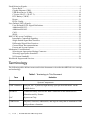
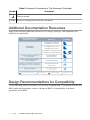
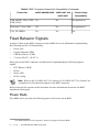
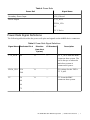
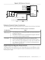
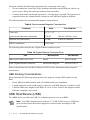
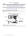
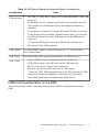
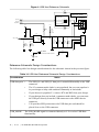
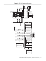
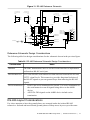
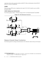
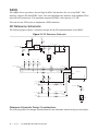
RIO MEZZANINE CARD DESIGN GUIDE
NI sbRIO-9607/9627
The NI sbRIO-9607 and sbRIO-9627 provide an embedded real-time processor, reconfigurable
FPGA, and a RIO Mezzanine Card (RMC) connector. The RMC connector is a high-density,
high-throughput connector that features 96 single-ended DIO lines directly connected to the
FPGA with the ability to add up to two C Series modules and additional peripherals. Develop
a custom RMC to integrate your own specific analog I/O, digital I/O, communication
capabilities, and signal conditioning by combining these components onto a mating printed
circuit board (PCB), known as an RMC.
In this document, the sbRIO-9607 and sbRIO-9627 are referred to inclusively as the sbRIO
device.
This document provides detailed information about RMC design techniques, guidelines, and
requirements.
Note Refer to the documents listed in the Additional Documentation Resources
section of this chapter for more information as you design, prototype, and implement
your sbRIO device application. In particular, refer to the NI sbRIO-9607 User
Manual and NI sbRIO-9627 User Manual for dimensions and pinout information
and the NI sbRIO-9607 Specifications and NI sbRIO-9627 Specifications for
specifications for your sbRIO device.
Contents
Terminology.............................................................................................................................. 2
Schematic Conventions.............................................................................................................3
Additional Documentation Resources...................................................................................... 4
Design Recommendations for Compatibility............................................................................4
Fixed Behavior Signals............................................................................................................. 6
Power Rails....................................................................................................................... 6
Gigabit Ethernet (GBE).................................................................................................... 9
USB Host/Device (USB)................................................................................................ 12
C Series (SLOT 1, SLOT 2)............................................................................................18
RTC Battery (VBAT)...................................................................................................... 20
Resets.............................................................................................................................. 21
FPGA Config.................................................................................................................. 23
User-Defined FPGA Signals................................................................................................... 24
User-Defined FPGA Signal Definitions..........................................................................24
Additional RS-232.......................................................................................................... 24
Additional RS-485.......................................................................................................... 26
CAN................................................................................................................................ 28
SDIO............................................................................................................................... 30
RMC PCB Layout Guidelines.................................................................................................32
Impedance-Controlled Signaling.................................................................................... 33
Single-Ended Signal Best Practices................................................................................ 33
Differential Signal Best Practices................................................................................... 34
Ground Plane Recommendations....................................................................................34
Fanout and Layout Options.............................................................................................34
Mechanical Considerations..................................................................................................... 34
Selecting an Appropriate Mating Connector.................................................................. 35
Selecting Appropriate Standoffs..................................................................................... 35
NI Custom Standoffs.......................................................................................................36
Worldwide Support and Services............................................................................................ 36
Terminology
The following table defines terms used in this document to describe the sbRIO device concepts
and technology.
Table 1. Terminology in This Document
Term
Definition
System Components
RMC connector
240-pin, 40 × 6 position, high-density open pin field SEARAY on the
sbRIO device.
SEARAY
Connector family used for the RMC connector on the sbRIO device.
Manufactured by Samtec.
SoC
System on Chip.
USB Device
Physical, electrical, addressable, and logical entity that is attached to USB
and performs a function.
2
|
ni.com
|
NI sbRIO-9607/9627 RMC Design Guide
Table 1. Terminology in This Document (Continued)
Term
Definition
USB Device port Port on an RMC that provides a USB Device interface to the sbRIO
device.
USB Host
USB interface that controls the bus and communicates with connected
USB devices.
USB Host port
Port on an RMC that provides a USB Host interface from the sbRIO
device.
Reference Schematic and Signal Naming
LVTTL
In compliance with the Low-Voltage Transistor-Transistor Logic
(LVTTL) specification.
LVCMOS
In compliance with the Low-Voltage Complementary Metal Oxide
Semiconductor (LVCMOS) specification.
Schematic Conventions
The following table describes symbol conventions used in the I/O interface schematic
diagrams in this document.
Table 2. Schematic Conventions in This Document
Symbol
Description
Off-page symbol that represents communication to and from the mating connector.
Off-page symbol that represents communication from the mating connector.
Off-page symbol that represents communication to the mating connector.
On-page symbol that represents the signal being driven.
On-page symbol that represents the signal being received.
Power supply rail.
I
Analog ground.
Digital ground.
NI sbRIO-9607/9627 RMC Design Guide |
© National Instruments
|
3
Table 2. Schematic Conventions in This Document (Continued)
Symbol
Description
Chassis ground.
SPARE Refers to an unpopulated reference designator.
Additional Documentation Resources
Refer to the following additional resources as you design, prototype, and implement your
sbRIO device application.
What Would You Like to
Learn More About?
Resources
Availability
NI sbRIO-9607 User Manual
NI sbRIO-9627 User Manual
NI sbRIO-9607
NI sbRIO-9627
NI sbRIO-9607 Specifications
NI sbRIO-9627 Specifications
NI sbRIO-9607 Getting Started Guide
NI sbRIO-9627 Getting Started Guide
Designing a RIO Mezzanine Card
for your application
NI sbRIO-9607/9627
RMC Design Guide
Adding an sbRIO-9607/sbRIO-9627
target in LabVIEW
LabVIEW Help (NI-RIO)
Creating a socketed CLIP that defines the
I/O configuration to use in your application
NI Single-Board RIO CLIP
Generator Help
NI Training and Support
ni.com/singleboard/setup
ni.com/training
ni.com/support
PDF available online at ni.com/manuals
Help file available locally
Included in the shipping kit
Available online at ni.com
Design Recommendations for Compatibility
Use the following table to determine if a previously designed RMC is compatible with the new
RMC pinout and as guidance on how to design an RMC for compatibility with future
generations of the RMC.
4
|
ni.com |
NI sbRIO-9607/9627 RMC Design Guide
Table 3. RMC Connector Feature Set Compatibility
Feature Set
sbRIO-9605/06/23/26 sbRIO-9607 and
sbRIO-9627
Future Design
Compatibility
DIO[0..63]
Yes
Yes
Yes
DIO[64..95]
Yes
Yes
Not guaranteed
FPGA_CONF
Yes
Yes
Yes
USB_D+/-
Yes
Yes
Yes
RST#
Yes
Yes
Yes
SYS_RST#
Yes
Yes
Yes
5V
Yes
Yes
Yes
3.3V_AUX
Yes
Yes
Yes
FPGA_VIO
Yes
Yes
Yes
PROC_VIO
Yes
No1
Not guaranteed
VBAT
Yes
Yes
Yes
GP_PORT
CAN
RS-232
RS-485
Secondary Ethernet
SDHC
Yes
No
Not guaranteed
Processor I/O via
DIO[0..95]
CAN
RS-232
RS-485
SDHC
No
Yes
Not guaranteed
GBE_MDI[0..3+/-]
No
Yes
Not guaranteed
1
Pin 42 - RESERVED of the RMC connector provides 3.3 V to the RMC in order to maintain
compatibility with the sbRIO-9605/06/23/26 RMC pinout. This pin is not recommended for use
with new designs.
NI sbRIO-9607/9627 RMC Design Guide |
© National Instruments
|
5
Table 3. RMC Connector Feature Set Compatibility (Continued)
Feature Set
sbRIO-9605/06/23/26 sbRIO-9607 and
sbRIO-9627
USB_MODE, USB_CPEN, No
USB_VBUS
Future Design
Compatibility
Yes
Not guaranteed
Dedicated C Series DIO
No2
Yes
Not guaranteed
VIN_FILTERED
No
Yes
Yes
Fixed Behavior Signals
A subset of pins on the RMC connector on the sbRIO device are dedicated to implementing
the following specific I/O functionality:
•
Power rails
•
Gigabit Ethernet (GBE)
•
USB Host/Device (USB)
•
C Series (SLOT 1, SLOT 2)
Other pins on the RMC connector are dedicated to implementing the following support
signals:
•
RTC Battery (VBAT)
•
Resets
•
Status LED
•
FPGA Config
Note Refer to the NI sbRIO-9607 User Manual or NI sbRIO-9627 User Manual for
a complete list of all pins and signals on the RMC connector.
Refer to the specific sections in this document for more information about how the RMC
implements each signal.
Power Rails
The sbRIO device provides the following power rails for use on an RMC:
2
6
|
The sbRIO-9605/06/23/26 supports C Series I/O using the NI 9693 RMC.
ni.com |
NI sbRIO-9607/9627 RMC Design Guide
Table 4. Power Rails
Power Rail
Signal Name
Secondary Power Input
VIN_Filtered
Power Output
3.3V_AUX
FPGA_VIO
5V
5V C Series
Power Rails Signal Definitions
The following table describes the power rails pins and signals on the sbRIO device connector.
Table 5. Power Rails Signal Definitions
Signal Name Dedicated Pin #
Direction
(from Host
System)
I/O Standard
Description
3.3V_AUX
48
O
—
3.3 V_AUX from the RMC
connector host system. The
rail is always on when the
main host system is
connected to power.
FPGA_VIO
234
O
—
I/O voltage for the FPGA
3.3 V pins.
O
—
5 V from the RMC
connector host system.
240
5V
54
60
66
72
NI sbRIO-9607/9627 RMC Design Guide |
© National Instruments
|
7
Table 5. Power Rails Signal Definitions (Continued)
Signal Name Dedicated Pin #
5V C Series
86
Direction
(from Host
System)
I/O Standard
O
5V
Signal-conditioned C Series
DIO.
I
—
9 V to 30 V input to power
the sbRIO device through
the RMC connector rather
than through the front panel
connector.
91
VIN_Filtered 1
Description
7
14
20
VIN_Filtered Implementation on the RMC
The following figure shows a schematic design for the VIN_Filtered implementation on the
RMC.
Figure 1. VIN_Filtered Reference Schematic
VIN_EXT +
9 V - 30 V
F1
7A
125 Vac
60 Vdc
EMI-COMM-MODE,SM
27440445447
C
SMCJ33CA-13-F
2
33 V
C90
CR19
1
VIN_EXT –
1000 PF
1%
50 V
COG
3
1
A
4
2
VIN_RMC
2
L19
C91
1
1000 PF
1%
50 V
COG
GND
Connect a well-regulated voltage that falls in the range of 9 V to 30 V to the VIN_Filtered pins
to power up the board.
Include a common mode choke in the design before connecting the voltage rails to the RMC
connector. Place a transient voltage suppressor before the common choke. NI recommends
including a fuse in your design to protect the voltage transient suppressor.
Reference Schematic Design Considerations
The following table lists design considerations for the schematic shown in the previous figure.
8
|
ni.com |
NI sbRIO-9607/9627 RMC Design Guide
Table 6. Power Rails Reference Schematic Design Considerations
Consideration
Notes
TVS Selection
The recommended part is SMCJ33CA-13-F from Diodes. Any TVS
with reverse standoff voltage and breakdown voltage of more than
30 V can be designed in.
Common Mode
Choke
The recommended part is 2744045447 from Fair-Rite. Alternatively,
use a common mode choke that matches the performance of this part
in terms of the DC and AC impedance.
Capacitor
1000 pf is the recommended value of the decoupling input and output
capacitor. The recommended part is a ceramic COG.
Fuse
The recommended part is TR1/6125TD7-R from Eaton if the only
load after the fuse is the VIN_RMC input pin to the sbRIO device.
Use a 7 A fuse to provide sufficient margin and prevent false blows
due to temperature and process variations. If you choose to connect
other loads after the fuse, you must account for the extra current
drawn by that load when selecting a fuse.
Gigabit Ethernet (GBE)
The sbRIO device provides a secondary Gigabit Ethernet port (GBE) for use on an RMC.
GBE Signal Definitions
The following table describes the GBE port pins and signals on the sbRIO device connector.
NI sbRIO-9607/9627 RMC Design Guide |
© National Instruments
|
9
Table 7. GBE Signal Definitions
Signal Name
Dedicated Pin #
GBE_MDI0+
3
GBE_MDI0-
9
GBE_MDI1+
16
GBE_MDI1-
22
GBE_MDI2+
5
GBE_MDI2-
11
GBE_MDI3+
18
GBE_MDI3-
24
GBE_SPEED_LEDg 37
Direction
(from Host
System)
I/O Standard
I/O
Defined by
Ethernet PHY
specification
Pre-magnetic
Gigabit Ethernet
data pairs.
O
LVTTL3.3V
Speed LED
signals.
O
LVTTL3.3V
Activity/link
LED signal.
GBE_SPEED_LEDy 31
GBE_ACT_LEDg
32
Description
GBE Implementation on the RMC
The following figure shows a schematic design for the GBE implementation on the RMC.
10
|
ni.com
|
NI sbRIO-9607/9627 RMC Design Guide
Figure 2. GBE Reference Schematic
J3
GBE0_MDIO_P
GBE0_MDIO_N
GBE0_MDI1_P
GBE0_MDI1_N
GBE0_MDI2_P
GBE0_MDI2_N
GBE0_MDI3_P
GBE0_MDI3_N
2
2
2
2
2
2
2
2
11
10
4
5
3
2
8
9
12
6
1
7
1
2
C7
1
0.1UF
10%
16V 2
C8
1
0.1UF
10%
16V 2
C2
1
0.1UF
10%
16V 2
13
14
15
16
C4
0.1UF
10%
16V
MDIA_P
MDIA_N~
MDIB_P
MDIB_N~
MDIC_P
MDIC_N~
MDID_P
MDID_N~
MCTA
MCTB
MCTC
MCTD
17
SHIELD1
18
SHIELD2
LED1(GRN-CATH)
LED1(GRN-AN)
LED2(GRN-CATH/YEL-AN)
LED2(GRN-AN/YEL-CATH)
08261K1T-43-F
GBE0_ACT_LEDg
2
2
R5
1
475 1%
1/16 W
GBE0_SPEED_LEDy
GBE0_SPEED_LEDg
2
2
2
R6
1
475 1%
1/16 W
Reference Schematic Design Considerations
The following table lists design considerations for the schematic shown in the previous figure.
Table 8. GBE Reference Schematic Design Considerations
Consideration
Notes
MDI data pairs •
•
LED signals
•
•
•
The MDI data pairs are routed differentially and connected directly to
the Ethernet connector.
The Ethernet connector has the required Ethernet magnetics built into
it. You may use discrete magnetics instead.
You can use the LED signals to directly drive connector LEDs.
Size the current-limiting resistors to not exceed 8 mA drive current.
Refer to the Ethernet Speed LED Behavior table of the NI sbRIO-9607
User Manual or NI sbRIO-9627 User Manual for information about
Ethernet LED signal behavior.
Gigabit Ethernet Magnetic Requirements
The Ethernet PHY on the sbRIO device uses voltage-mode drivers for the MDI pairs, which
greatly reduces the power that the magnetics consume and eliminates the need for a sensitive
center tap power supply.
NI sbRIO-9607/9627 RMC Design Guide |
© National Instruments
|
11
You must consider the following requirements for connecting center taps:
•
Do not connect the center taps of the isolation transformer on the MDI pair side to any
power source. Keep the center taps separate from each other.
•
Connect each center tap through separate 0.1 μF capacitors to ground. The separation is
required because the common-mode voltage on each MDI pair might be different.
The following table lists recommended magnetic characteristics.
Table 9. Recommended Magnetic Characteristics
Parameter
Value
Test Condition
Turns ratio
1 CT : 1 CT
—
Open-circuit inductance (minimum)
350 μH
100 mV, 100 kHz, 8 mA
Insertion loss (maximum)
1.0 dB
0 MHz to 100 MHz
HIPOT (minimum)
1500 Vrms
—
The following table describes the Gigabit Ethernet connector parts.
Table 10. Gigabit Ethernet Connector Parts
Part
Manufacturer
Part Number
sbRIO-9607/sbRIO-9627 PHY
Micrel
KSZ9031RNX
RMC Gigabit Ethernet connector
Bel Stewart Magjack
0826-1K1T-43-F
Refer to the datasheet for the Micrel Ethernet PHY for more information about magnetic
requirements.
GBE Routing Considerations
NI recommends the following design practices for properly routing GBE signals on your
RMC:
•
Route MDI pairs differentially with 100 Ω differential trace impedance.
•
Length-match the positive and negative signal for each MDI data pair to within 10 mils.
•
Limit the MDI trace lengths on the RMC to 6.0 in. or less, which is the length at which
Ethernet compliance was tested.
USB Host/Device (USB)
The sbRIO device provides one USB 2.0-compliant ports for use on an RMC.
Note Your RMC design must provide the 5 V USB_VBUS power to USB Host
ports and must limit the current supplied to each host port according to USB
specifications.
12
|
ni.com |
NI sbRIO-9607/9627 RMC Design Guide
USB Host/Device Signal Definitions
The following table describes the USB Host/Device port pins and signals on the sbRIO device
connector.
Table 11. USB Host/Device Signal Definitions
Signal Name
Dedicated
Pin #
USB_D+
29
USB_D-
35
USB_MODE 34
Direction
(from Host
System)
I/O Standard
Description
I/O
Defined by USB
specification
Port for hi-speed
differential USB.
I
—
Connect to digital ground
or leave disconnected to
configure the USB port as
Host.
Connect to +3.3V to
configure the USB port as
Device.
USB_CPEN
33
USB_VBUS 84
O
LVTTL3.3V
USB over-current
protection enable.
I
5 V tolerant
voltage sense
USB VBUS input. Allows
USB PHY to sense if
VBUS is present on the
connector.
Configuring the USB Mode
You can configure the USB interface to be a USB Host port or a USB Device port, as shown in
the following table. This mode is set when the system boots and does not change dynamically.
Note USB On-The-Go (OTG) is not supported.
NI sbRIO-9607/9627 RMC Design Guide |
© National Instruments
|
13
Table 12. Configuring the USB Mode
Mode
How to Enable
USB Host
Connect the USB_MODE signal to digital ground or leave disconnected on
your RMC. Refer to the USB Host Implementation on the RMC section for
more information about the USB Host implementation on the RMC.
USB Device Connect the USB_MODE signal to the +3.3V rail on your RMC. Refer to the
USB Device Implementation on the RMC section for more information about
the USB Device implementation on the RMC.
USB Device Implementation on the RMC
The following figure shows a schematic design for the USB Device implementation on the
RMC.
Figure 3. USB Device Reference Schematic
1
R78
2
These lines can swap
if layout is easier
0 5%
1/16W
Population Options
For EMC/EMI
L2
2
USB_DN
2
USB_DP
4
3
1 D+
2 D–
DLW21S_900
+3.3V
U17
R7
TPD2EUSB30
0 5%
1/16 W
Not Populated
2
1 R76 2
3 GND
0 5%
1/16 W
2
USB_VBUS
1
R66
2
0 5% 1
1/16 W
2
C32
1
1.0 UF
10% 2
16 V
1
2
3
4
C33
0.1 UF
10%
16 V
1
R61
2
Spare
R0603
J8
VBUS
D–
D+
GND
USB_MODE
Pulled Up To Select USB Device Port
C204
12
0.1 UF 10%
50 V
5 SHLD1
6 SHLD2
CONN-USB, B, HIGH_RETENTION
Reference Schematic Design Considerations
The following table lists design considerations for the schematic shown in the previous figure.
14
|
ni.com
|
NI sbRIO-9607/9627 RMC Design Guide
Table 13. USB Device Reference Schematic Design Considerations
Consideration
Notes
USB data pairs •
•
•
•
•
The USB_D+ and USB_D- data pair is routed differentially to the USB
connector.
On the RMC, the L2 common-mode choke is not populated, but you
can populate it in your design to help with conducted immunity or
emissions.
If you choose to populate L2, remove R76 and R78 from your design.
If your design does not include a common-mode choke, you can route
the USB pair directly from the USB connector to the sbRIO device
connector.
U17 provides ESD protection to the USB data pair and should be
placed close to the USB connector.
USB_MODE
The USB_MODE signal is connected directly to 3.3 V to select USB
Device functionality.
USB_CPEN
Leave the USB_CPEN signal disconnected for a USB Device port.
USB_VBUS
•
•
•
•
For the USB Device port to function properly, connect the
USB_VBUS signal to the VBUS pin on the USB connector.
This is a low-current, voltage-sense connection.
In layout, you can treat this connection as a data signal.
Connect the USB_VBUS signal directly to the VBUS pin on the USB
connector or connect through R66, which must be a 0 Ω jumper.
Overvoltage protection is included on the sbRIO device.
USB Host Implementation on the RMC
The following figure shows a schematic design for the USB Host implementation on the
RMC.
NI sbRIO-9607/9627 RMC Design Guide |
© National Instruments
|
15
Figure 4. USB Host Reference Schematic
R82
1
2
0 5%
1/16 W
These lines can swap
if layout is easier
POPULATION OPTIONS
FOR EMC/EMI
2
USB_DN
4
2
USB_DP
U18
TPD2EUSB30
2
3
DLW21S_900
NOT POPULATED
2
USB_VBUS
L3
1
+5 V
+5 V
1
2
R92
0 5%
C57
0.1 UF
10%
16 V
R79
1
1
1
2
2
1
2
D+
D–
2
0 5%
1/16 W
R86
4.7 K
0.5%
1/16 W
3 GND
U20
6
4
2
USB_CPEN
2
1
2
R85
4.7 K
0.5%
1/16 W
1
2
IN
FAULT~
EN
GND
PA D
ILIM
R89
23.2 K
0.5%
1/16 W
1
1
2
3
4
3
5
7
1
–
TPS2553
2
2
R7
J10
OUT
1
C67
100 UF
6.3 V
20% 2
1
C62
22 UF
25 V
2
10%
1
USB_MODE
1
C61
0.01 UF
100 V
10%
2
C203
R93
1K
0.5%
5
6
VCC
–DAT1
+DAT1
GND
SHLD1
SHLD2
USB_A
2
0.1 UF 10%
50 V
Pulled Down To Select USB Host Port
0 5%
1/16 W
Reference Schematic Design Considerations
The following table lists design considerations for the schematic shown in the previous figure.
Table 14. USB Host Reference Schematic Design Considerations
Consideration
Notes
USB data pairs •
•
•
•
•
USB_MODE
16
|
ni.com
|
The USB_D+ and USB_D- data pair is routed differentially to the USB
connector.
The L3 common-mode choke is not populated, but you can populate it
in your design to help with conducted immunity or emissions.
If you choose to populate L3, remove R79 and R82 from your design.
If your design does not include a common-mode choke, you can route
the USB pair directly from the USB connector to the sbRIO device
connector.
U18 provides ESD protection to the USB data pair and should be
placed close to the USB connector.
The USB_MODE signal is connected directly to 0 V to select USB Host
functionality.
NI sbRIO-9607/9627 RMC Design Guide
Table 14. USB Host Reference Schematic Design Considerations (Continued)
Consideration
Notes
USB_CPEN
Connect the USB_CPEN signal to the enable of the VBUS current limit
switch (U20) so that the sbRIO device can power-cycle USB devices when
the processor is reset.
USB_VBUS
•
•
•
•
•
•
•
•
For the USB Host port to function properly, connect the USB_VBUS
signal to the VBUS pin on the USB connector.
This is a low-current, voltage-sense connection.
In layout, you can treat the trace after R92 going to the sbRIO device
connector as a data signal.
Connect the USB_VBUS signal directly to the VBUS pin on the USB
connector or connect through R92, which must be a 0 Ω jumper.
Overvoltage protection is included on the sbRIO device.
The RMC must provide 5 V VBUS power for the USB Host port.
A current limit switch is required between the 5 V rail and the USB
connector.
U20 is the current limiter.
NI recommends that you provide 100 μF capacitance on the VBUS
rail.
Supporting Onboard USB Devices
When you implement a USB device directly on your RMC, you can connect the device to a
USB Host port from the sbRIO device. For this case, use the following design guidelines:
•
You can connect the USB data pair directly to a USB device on your RMC.
•
A current limiter is not required.
•
Use the RST# signal to reset the USB device when the sbRIO device is in reset.
•
Tie the USB_VBUS signal to 5 V.
USB Routing Considerations
NI recommends the following design practices for properly routing USB signals on your
RMC:
•
Route the USB_D+ and USB_D- signals as differential pairs with 90 Ω differential
impedance.
•
Length-match the positive and negative signal for each USB data pair to within 10 mils.
•
Limit the USB_D+ and USB_D- trace lengths on the RMC to 8.0 in. or less, which is the
length at which USB compliance was tested.
NI sbRIO-9607/9627 RMC Design Guide |
© National Instruments
|
17
C Series (SLOT 1, SLOT 2)
The sbRIO device provides two C Series slots for use on an RMC, which is Slot 1 and Slot 2.
C Series Signal Definitions
The following table describes the C Series slot pins and signals on the sbRIO device
connector.
Table 15. C Series Signal Definitions
Signal Name
Dedicated Pin # Direction (from I/O Standard
Host System)
Slot 1 Slot 2
ID_SELECT#[x]
40
63
I/O
OSCLK_DIO0[x]
58
76
LVTTL5V
TRIG_DIO1[x]
64
82
tolerant input
DONE#_DIO2[x]
50
68
CVRT#_DIO3[x]
46
69
SPIFUNC_DIO4[x] 53
77
SPICS#_DIO5[x]
55
73
MISO_DIO6]x]
71
81
MOSI_DIO7[x]
56
74
SPI_CLK[x]
61
79
SLEEP[x]
45
51
5V C Series
86
91
O
LVTTL3.3V
Description
Signal-conditioned
C Series DIO.
5V
C Series Implementation on the RMC
The following figures show schematic designs for the C Series implementation on the RMC.
18
|
ni.com
|
NI sbRIO-9607/9627 RMC Design Guide
Figure 5. C Series with Current Limiter Reference Schematic
CURRENT LIMITER
+5V_C_SERIES
1
R1
2
64.9 K
0.5%
1/16 W
U18
2
3
8
NC_CSERIES_PWR_FAULT1~
4
2
0.1 UF
10%
16 V
C1
1
IN1
IN2
FAULT~
EN
6
7
OUT1
OUT2
VCC_SLOT
5
ILIM
CSERIES_PWR_ILIM
1
9
GND
THERMPAD
1
150 K
1%
1/16 W
R3
TPS2557
IOS_max = 869 mA
IOS_min = 592 mA
2
J21
DSUB 15, PLUG-762243-01
ID_SELECT
~S~P~I~C~S_DIO5
NC_RESERVED
L3
1
VCC_SLOT
2
VCC_SLOT1_FILT
C124
1
2
0.1 UF
10%
16 V
C125
0.1 UF
10%
16 V
9
~C~O~N~V~E~R~T_DIO3
10
OVERSAMPLECLK_DIO0
3
11
SPI_CLK
4
12
6.8 UH
2
1
2
1
1
100 UF
20%
6.3 V
C126
2
1
0.01 UF
10%
16 V
C127
2
TRIG_OUT_DIO1
MOSI_DIO7
SPIFUNC_DIO4
MISO_DIO6
5
13
NC_RESERVED13
6
14
7
15
~D~O~N~E_DIO2
8
BUFF_SLEEP
VCC_SLOT
2
C128
1
16
17
0.1 UF
10%
16 V
5
VCC
2
SLEEP
A
U15
LVC1G126
R800
1
4
OE
GND
2
332
1/16 W
1
3
VCC_SLOT
Figure 6. C Series without Current Limiter Reference Schematic
J21
DSUB 15, PLUG-762243-01
ID_SELECT
~S~P~I~C~S_DIO5
NC_RESERVED
L3
1
+5V_C_SERIES
2
2
1
0.1 UF
10%
16 V
9
~C~O~N~V~E~R~T_DIO3
10
3
11
4
12
6.8 UH
C124
VCC_SLOT1_FILT
1
2
2
C125
1
0.1 UF
10%
16 V
1
C126
2
100 UF
20%
6.3 V
1
C127
2
0.01 UF
10%
16 V
TRIG_OUT_DIO1
MOSI_DIO7
SPIFUNC_DIO4
SLEEP
5
13
6
OVERSAMPLECLK_DIO0
SPI_CLK
MISO_DIO6
NC_RESERVED13
14
7
15
8
16
~D~O~N~E_DIO2
17
Use a current limiter to protect the PI inductor from overcurrenting in a fault condition and
prevent the 5 V pin from accidentally shorting to either GND or CHSY. This protection is
beneficial in environments where hot-plugging C Series modules are used.
Reference Schematic Design Considerations
The following table lists design considerations for the schematics shown in the previous
figures.
NI sbRIO-9607/9627 RMC Design Guide
|
© National Instruments
|
19
Table 16. C Series Reference Schematic Design Considerations
Consideration
Notes
Current limiter U18 If a current limiter is used, you must re-buffer the sleep signal to the
DSUB connector. If a current limiter is not used, you can connect the
sleep signal directly to the DSUB connector by removing U15 in the
schematic. The buffer prevents the sleep signal from being driven to
the C Series module in an overcurrent condition.
Inductor L3
Power PI Filter specifications:
•
Value: 6.8 μH ±20%
•
ESR: <200 mΩ
•
Rated Current: >=400 mA
Capacitor C126
Power PI Filter specifications:
•
Value: 100 μF ±20%
•
ESR: <100 mΩ
C Series Routing Considerations
NI recommends the following design practices for properly routing C Series signals on your
RMC3:
•
Route the signals with 55 Ω ±10% impedance.
•
Length-match each signal to within 250 mils.
•
Limit each signal trace length on the RMC to 10.0 in. or less, which is the length from the
RMC SEARAY connector to DSUB connector.
•
Maintain at minimum a 3 × H line spacing between single-ended traces, where H is the
distance in the board stack-up from the trace to its reference plane.
RTC Battery (VBAT)
The RMC contains a lithium cell battery that maintains the real-time clock (RTC) on the
sbRIO device when the sbRIO device is powered off. A slight drain on the battery occurs
when power is not applied to the sbRIO device. The following table lists the VBAT power
specifications.
3
20
|
SLEEP lines and 5V_C SERIES are exempted from these requirements.
ni.com |
NI sbRIO-9607/9627 RMC Design Guide
Table 17. VBAT Power Specifications
Specification
Minimum
VBAT input voltage
2.875 V
Typical
Maximum
3.0 V
5.5 V
sbRIO device powered VBAT current
—
25 nA
100 nA
sbRIO device unpowered VBAT current
—
2.6 μA average
4.2 μA average
If the battery is dead, and if no voltage has been applied to the VBAT pins, the system still
starts but the system clock resets to the UNIX epoch date and time.
VBAT Signal Definitions
The following table describes the VBAT pins and signals on the sbRIO device connector.
Table 18. VBAT Signal Definitions
Signal
Name
VBAT
Dedicated Pin # Direction (from I/O Standard
Host System)
236
I
Power rail
Description
RTC battery input that
provides backup power to
the RTC to maintain
absolute time.
VBAT Implementation on the RMC
The following figure shows a schematic design for the VBAT implementation on the RMC.
Figure 7. VBAT Reference Schematic
2
+
1
BTH1
–
BATHLDR-747921-01
VBAT
2
Use Br1225
Battery In
This Holder
Reference Schematic Design Considerations
You can directly connect the battery to VBAT. The sbRIO device already provides a currentlimiting resistor and reverse-voltage protection.
Resets
The sbRIO device provides signals for implementing a reset button on an RMC and indicating
that the sbRIO device is in reset.
NI sbRIO-9607/9627 RMC Design Guide |
© National Instruments
|
21
Reset Signal Definitions
The following table describes the Reset pins and signals on the sbRIO device connector.
Table 19. Reset Signal Definitions
Signal Name
Dedicated
Pin #
Direction
(from Host
System)
I/O Standard
Description
RST#
38
O
LVTTL3.3V
Reset that indicates that main
power is not adequate or that
the sbRIO device is in reset.
Asserted low.
SYS_RST#
43
I
LVTTL3.3V
System reset that puts the
sbRIO device in reset. Asserted
low.
Asserting this signal causes the
RST# signal to also assert.
You can also assert this signal
to put the sbRIO device into
safe mode or reset IP address
settings.
Reset Implementation on the RMC
The following figure shows a schematic design for the Reset implementation on the RMC.
Figure 8. Reset Reference Schematic
+3.3 V
1
SYS_RST#
2
1
1
2
R2
2
2
R4
1K
0.5%
RESET_SW#
68.1 0.5%
1/16 W
C3
C0402
SPA RE
2
4
3
1
SW3
720176-01
Refer to the SYS RST# and RMC RST# sections of the NI sbRIO-9607 User Manual or
NI sbRIO-9627 User Manual for more information about the behavior of the Reset signals.
Reference Schematic Design Considerations
The following table lists design considerations for the schematic shown in the previous figure.
22
|
ni.com
|
NI sbRIO-9607/9627 RMC Design Guide
Table 20. Reset Reference Schematic Design Considerations
Consideration
Notes
Series termination When SYS_RST# is driven, you must place a series termination resistor
at the driver. When the driver is a mechanical switch, placing series
termination is especially important due to the low output impedance of
the switch.
FPGA Config
The sbRIO device provides an FPGA Config signal to indicate when the FPGA is configured.
FPGA Config Signal Definitions
The following table describes the FPGA Config pins and signals on the sbRIO device
connector.
Table 21. FPGA Config Signal Definitions
Signal Name
Dedicated
Pin #
FPGA_CONF 239
Direction
(from Host
System)
O
I/O Standard
Description
Refer to the
NI sbRIO-9607 User
Manual or
NI sbRIO-9627 User
Manual for more
information about the
behavior of this signal.
FPGA Config
Asserts when the
FPGA is
configured.
Asserted high when
the FPGA has been
programmed.
FPGA Config Implementation on the RMC
The following figure shows a schematic design for the FPGA Config implementation on the
RMC.
Figure 9. FPGA Config Reference Schematic
DS3
FPGA_CFG
2, 3, 4
1
R128
357 0.5%
1/16 W
GRN
2
1
2
LED_GRN_735278-01
Refer to the FPGA_CONF section of the NI sbRIO-9607 User Manual or NI sbRIO-9627 User
Manual for more information about the behavior of the FPGA Config signal.
NI sbRIO-9607/9627 RMC Design Guide
|
© National Instruments
|
23
User-Defined FPGA Signals
The sbRIO device connector provides several FPGA pins that you can configure for purposes
specific to your application. In addition to FPGA Digital I/O (DIO), you can use these pins to
implement the following run-time peripheral interfaces:
•
RS-232
•
RS-485
•
CAN
•
SDIO
Refer to the specific sections in this chapter for more information about how the RMC
implements each signal.
Note To read or write to this I/O from a LabVIEW project, you must use the sbRIO
CLIP Generator application to create a socketed component-level IP (CLIP) that
defines the I/O configuration of the sbRIO device to use in your application. Refer to
the NI Single-Board RIO CLIP Generator Help for more information about creating
a CLIP.
User-Defined FPGA Signal Definitions
The following table describes the 96 user-defined FPGA pins and signals on the sbRIO device
connector.
Table 22. User-Defined FPGA Signal Definitions
Signal Name Direction (from Host I/O Standard
System)
DIO [0..95]
I/O
LVTTL3.3V
Description
Pins for connecting directly to the
FPGA through a series resistor and for
enabling serial, CAN, or SDHC
peripherals on an RMC.
Additional RS-232
You can use any FPGA pins to implement additional RS-232 ports.
Number of interfaces:
•
sbRIO-9607—4 (Serial2, Serial3, Serial4, Serial5)
•
sbRIO-9627—4 (Serial4, Serial5, Serial6, Serial7)
RS-232 Reference Schematic
The following figure shows a schematic design for the RS-232 implementation on the RMC.
24
|
ni.com |
NI sbRIO-9607/9627 RMC Design Guide
Figure 10. RS-232 Reference Schematic
+3.3V
2
C176
0.1 UF
10%
16 V
1
+3.3V
R81
1K
0.5%
2
R87
1
R83
2
9
28
6
2
39 0.5%
1/16W
2
R88
39 0.5%
1/16W
1
R84
2
8
16
39 0.5%
1/16W
2
3
V-
C2DIN1
DIN2
DIN3
ROUT1
ROUT2
ROUT3
ROUT4
ROUT5
25
23
22
DOUT1
DOUT2
DOUT3
RIN1
RIN2
RIN3
RIN4
RIN5
SERIAL2_CD_F
SERIAL2_DSR_F
SERIAL2_RX_F# +3.3V
SERIAL2_CTS_F
SERIAL2_RI_F
27
VCC
FORCEON
FORCEOFF~
GND
INVA LID~
THERMALPA D
NC1
NC2
SERIAL2_TX_F#
SERIAL2_RTS_F
SERIAL2_DTR_F
21
20
19
18
17
26
1
24
32
NC3
NC4
C175
0.1 UF
10%
16 V
2
33
TRS3253EIRSMR
39 0.5%
1/16W
+3.3V
+3.3V
1
1
2
R145
SPA RE
R0402
2
R80
4.7 K
0.5%
1/16 W
1
2,3
C83
2
C0603, SPA RE
1
R147
4.7 K
0.5%
1/16 W
2
1
C82
2
C0603, SPA RE
1
C81
2
C0603, SPA RE
+3.3V
1
C76
1800 PF
50 V
5%
2
C0603, SPA RE
R163
1
SERIAL2_SIGNAL_GND_232
2
0 5%
1/16W
1
SERIAL2_RI_F
R162
2
SERIAL2_RI_CONN
0 5%
1/16W
SERIAL2_DTR_F
R161
1
SERIAL2_DTR_CONN
2
J11
DSUB9-761918-A
0 5%
1/16W
1
SERIAL2_CTS_F
R160
2
SERIAL2_CTS_CONN
SERIAL2_RTS_CONN
5
9
4
8
3
7
2
6
1
SERIAL2_RX_CONN#
10
11
0 5%
1/16W
SERIAL2_TX_F#
R159
1
SERIAL2_TX_CONN#
2
0 5%
1/16W
1
SERIAL2_RTS_F
SERIAL2_RX_F#
R153
1
2
1
SERIAL2_DSR_F
SERIAL2_CD_F
R155
2
0 5%
1/16W
0 5%
1/16W
1
R152
R154
5
1
9
2
C80
1
FPGA_CFG
C1C2+
4
SERIAL2_RI#
1
2
4
5
7
14
13
12
11
10
30
V+
C1+
8
SERIAL2_CTS#
39 0.5%
1/16W
1
2
2
2
2
31
1
2
VL
3
SERIAL2_RX
29
7
SERIAL2_DSR#
15
2
SERIAL2_DCD#
R90
1
C168
0.1 UF
10%
16 V
U19
2
0.1 UF 10%
50 V
2
2
2
2
C46
1
1
2
6
SERIAL2_TX
SERIAL2_RTS#
SERIAL2_DTR#
C48
1
0.1 UF 10%
50 V
1
C171
0.1 UF
10%
16 V
1
2
2
SERIAL2_DSR_CONN
0 5%
1/16W
2
0 5%
1/16W
SERIAL2_CD_CONN
1
C63
2
C0603, SPA RE
1
Caps are placed
to reduce emissions.
Standard practice.
120pF, 220pF, 470pF, etc
can be used
C64
2
C0603, SPA RE
1
C65
2
C0603, SPA RE
1
C66
2
C0603, SPA RE
1
C84
2
C0603, SPA RE
1
C58
2
0.1 UF 10%
50V
1
R108 2
R0805, SPA RE
NI sbRIO-9607/9627 RMC Design Guide |
© National Instruments
|
25
Reference Schematic Design Considerations
The following table lists design considerations for the schematic shown in the previous figure.
Table 23. RS-232 Reference Schematic Design Considerations
Consideration
Notes
Interface
The RMC reference schematic demonstrates how to use the Serial2
interface to implement a null-modem RS-232 serial port.
Serial transceiver
U19 is the RS-232 serial transceiver that converts between RS-232 and
LVTTL signal levels. To minimize the impact of higher voltage signals
on your RMC, place the serial transceiver near the RS-232 connector.
Series termination •
•
FPGA
R83, R84, R87, R88, and R90 are the series termination for Serial2.
Use series termination at the serial transceiver on all signals being
driven to the sbRIO device.
All FPGA DIO signals on the sbRIO device include series
termination.
All serial port signals pass through the FPGA on the sbRIO device. The
FPGA_CONF signal is used to disable the serial transceiver when the
FPGA is not configured. Disabling the transceiver in this way prevents
any unwanted glitches on the RS-232 port.
Additional RS-485
You can use any FPGA pins to implement additional RS-485 ports.
Number of interfaces:
•
sbRIO-9607—2 (Serial6, Serial7)
•
sbRIO-9627—2 (Serial8, Serial9)
RS-485 Reference Schematic
The following figure shows a schematic design for the RS-485 implementation on the RMC.
26
|
ni.com |
NI sbRIO-9607/9627 RMC Design Guide
Figure 11. RS-485 Reference Schematic
0.1 uF and 0.01 uF
Across pin 2 and 1
10 uF and 0.1 uF
Across pin 8 and 9
0.1 uF and 0.01 uF
Across pin 19 and 20
10 uF and 0.1 uF
Across pin 12 and 11
+3.3V
Vcc_RS485_1
Vcc_RS485_1
1
2
+3.3V
+3.3V
10
2
1
2
GND1-3
GND1-4 Digital
Isolation iCoupler
6 DE
2
1
R140
4 RxD
2
39 0.5%
1/16W
2
SERIAL6_RX_EN
20
19
16
12
14
I
IGND0
Tranceiver
5 RE~
D
R
J7
DSUB9-761918-A
SERIAL6_RXN
SERIAL6_TXN
SERIAL6_RXP
SERIAL6_TXP
Y
Z
13
15
A
18
B
17
GND2-1
SERIAL6_TXP
SERIAL6_TXN
SERIAL6_RXP
I
IGND0
5
9
4
8
3
5
VDD1-2
SERIAL6_TX_EN
SERIAL6_RX
GND2-4
VISOIN
GND2-3
VISOOUT
GND2-2
GND1-2
SERIAL6_TX
2
DC-DC Converter
VDD1-1
7 TxD
I
IGND0
9
9
2
C155
0.1 UF
10%
16 V
4
8
isoPower
1
C156
0.01 UF
10%
100 V 2
1
8
3
GND1-1
ISOLATION BARRIER
2
2
C162
10 UF
10%
10 V
Vcc_RS485_1
U25
1
1
I
IGND0
I
IGND0
R141
10 K
1/16 W
0.5%
C161
0.1 UF
10%
16 V
3
1
C160
0.1 UF
10%
16 V
7
C159 2
10 UF
10%
10 V
1
2
C153
0.01 UF
10%
100 V
7
2
2
1
C154 1
0.1 UF
10%
16 V 2
6
1
1
2
6
+3.3V
10
11
SERIAL6_RXN
11
ADM2587E
I
IGND0
Reference Schematic Design Considerations
The following table lists design considerations for the schematic shown in the previous figure.
Table 24. RS-485 Reference Schematic Design Considerations
Consideration
Notes
Interface
The RMC demonstrates how to use the Serial6 interface to implement a
null-modem RS-485 serial port.
Serial transceiver
U25 is the RS-485 serial transceiver that converts between RS-485 and
LVTTL signal levels. This transceiver provides functional isolation of
the RS-485 signals to prevent ground loops from affecting the RS-485
signals.
Series termination •
•
R140 is the series termination for Serial6. Use series termination at
the serial transceiver on all signals being driven to the sbRIO
device.
All FPGA DIO signals on the sbRIO device include series
termination.
RS-485 Layout Considerations
Pay close attention to how the ground planes are arranged under the isolated RS-485
transceiver. Isolated and non-isolated ground planes overlap across layers to provide some
NI sbRIO-9607/9627 RMC Design Guide |
© National Instruments
|
27
capacitance between the grounds and help with EMC. Refer to the datasheet for the RS-485
transceiver for more information.
CAN
You can use any FPGA pins to implement the single CAN (CAN1) interface port available
through the RMC.
CAN Reference Schematic
The following figure shows a schematic design for the CAN implementation4 on the RMC.
Figure 12. CAN Reference Schematic
+3.3V
+5V
C113
0.1 UF
10%
16 V
1
2
C6
0.1 UF
10%
16 V
1
2
U2
CAN_RX
R8
1
2
6
4
2
2
49.9 0.5%
1/16 W
VCCB
VCCA
B
GND
A
DIR
1
3
5
CAN_RX_5V
74LVC1T45
+5V
+3.3V
+3.3V
+5V
R12
1K
0.5%
R11
1
1
2
R7
2
CAN_RX_5V_R
39 0.5%
1/16 W
CAN_TX_5V
2
39 0.5%
1/16 W
+5V
+3.3V
+3.3V
1
+5V
1
2
R130
1K
0.5%
1
C130
0.1 UF
10%
16 V
1
2
2
CAN_RS
2
+5V
2
C121
0.1 UF
10%
16 V
VCCB
B
GND
VCCA
A
DIR
74LVC1T45
1
3
5
1
R9
2
8
RXD
TXD
VCC
VREF
GND CANH
CANL
RS
PCA82C251T
1
5
5
9
4
NC_RESERVED1
NC_RESERVED2
7
6
8
3
CAN_CANH
CAN_CANL
7
2
6
1
NC_RESERVED3
R10
1K
0.5%
U6
6
4
2
C114
0.1 UF
10%
16 V
J4
DSUB9-761918-A
U3
4
1
3
74LVC1T45
5
1
3
5
9
VCCA
A
DIR
4
2
VCCB
B
GND
8
6
4
2
3
2
1
U4
2
CAN_TX
C117
0.1 UF
10%
16 V
7
1
1
2
R132
1K
0.5%
C120
0.1 UF
10%
16 V
6
2
1
1
10
11
2
2
CAN_RS_5V
39 0.5%
1/16 W
1
C11
2
0.1 UF 10%
50 V
Reference Schematic Design Considerations
The following table lists design considerations for the schematic shown in the previous figure.
4
28
|
The NXP PCA82C25IT CAN transceiver requires 5 V logic levels. The RMC uses external discrete
buffers to translate 3.3 V FPGA lines to 5 V logic levels.
ni.com |
NI sbRIO-9607/9627 RMC Design Guide
Table 25. CAN Reference Schematic Design Considerations
Consideration
CAN_RX,
CAN_TX, and
Notes
•
•
CAN_RS
•
•
•
•
CAN_CANH
and
•
•
CAN_CANL
•
The recommended CAN transceiver requires 5 V I/O.
U2, U4, and U6 provide level translation between the 3.3 V I/O on the
sbRIO device and the 5 V I/O on the transceiver. Use caution when
implementing this level translation.
The TXD and RS inputs of the CAN transceiver must remain high
during power-down and power-up of the sbRIO device and RMC. This
prevents glitches on the CAN bus that might disrupt communication
between other devices on the bus. The level translator IC in this
schematic prevents these glitches.
The level translator output remains at high impedance until both of its
power supply rails are powered to allow the 5 V power supply to
power-up before the 3.3 V power supply.
All signals have series termination at the outputs to prevent overshoot
or undershoot at the receivers.
All FPGA DIO signals on the sbRIO device include series termination.
Route these signals differentially with a 120 Ω differential trace
impedance.
Minimize the overall length of the traces so that you can place
termination resistors in the CAN cabling as close as possible to the
CAN transceiver.
Depending on your design requirements, you can also place the CAN
termination resistor on the RMC.
Termination Resistors for CAN Cables
The termination resistors should match the nominal impedance of the CAN cable and therefore
comply with the values in the following table.
Table 26. Termination Resistor Specification
Characteristic
Termination resistor
Value
100 Ω minimum
Condition
Minimum power dissipation: 220 mW
120 Ω nominal
130 Ω maximum
NI sbRIO-9607/9627 RMC Design Guide |
© National Instruments
|
29
SDIO
The sbRIO device provides a Secure Digital (SD) Card interface for use on an RMC. This
interface supports SD and SDHC cards. You can implement this interface with standard SD or
microSD card connectors. The maximum supported SDHC card capacity is 32 GB.
You can use any FPGA pins to implement a SDIO interface.
SD Reference Schematic
The following figure shows a schematic design for the SD implementation on the RMC.
Figure 13. SD Reference Schematic
+3.3 V
+3.3 V
1
2
1
6
4
4
2
1
1
R354
IN
EN
GND
PAD
ILIM
3.3 V_SD_CRD_PWR
1
3
2
5
7
2
R701
TPS2553
R694
1 K 1%
1/16 W
OUT
FAULT~
10 K 0.5%
1/16 W
1
105 K 1%
1/16 W
1
C284
1.0 UF
10%
16 V
2
1
C279
0.1 UF
10%
16 V
2
1
GRN
2
1
R763
R764
20 K 1%
1/20 W
20 K 1%
1/20 W
2
1
SD_D(2)
1
R693
22 5% 1/20 W
SD_D(1)
1
SD_D(0)
R690
R692
J6
SD_D(3)_R
2
22 5% 1/20 W
2
1
R689
SD_D(2)_R
SD_D(1)_R
2
22 5% 1/20 W
2
+3.3 V
R759
R761
20 K 1%
1/20 W
2
SD_CLK
4
SD_CMD
4
1
20 K 1%
1/20 W
+3.3 V
SD Socket
CONN9-764432-01-RA
R691
2
4
4
13
2 SD_CMD_R
22 5% 1/20 W
SD_ACTIVITY
4
2
R354
R738
10 K 1%
1/20 W
SD_WP
CLK
CMD
1
R733
SD_CD~
CD/D3
D2
D1
D0
2
1
+3.3 V
Vdd
10 CardDetect
11 Common
12 WP
3 Vss1
6 Vss2
1
1
1
9
8
7
5
2
SD_D(0)_R
22 5% 1/20 W
+3.3 V
4
Shield1
R762
2
+3.3 V
1
20 K 1%
1/20 W
DS2
LED
QTLP630
10 K 1%
1/20 W
2
1
1
R734
2
330
1/16 W
SD_CD_R~
49.9 1% 1/20 W
1
R744
2
49.9 1% 1/20 W
SD_WP_R
1
R760
2
+3.3 V
1
20 K 1%
1/20 W
SD_D(3)
2
C293
4.7 UF
10%
25 V
GRN
+3.3 V
1
4
2
DS2
LED
QTLP630
2
+3.3V
SD_D(3:0)
1
R702
332
1/16 W
1
2
LED-17-21SYGC
2
2
U23
LED-17-21SYGC
SD_PWR_EN
R349
1 K 1%
1/16 W
C434
0.1 UF
10% 16 V
Reference Schematic Design Considerations
The following table lists design considerations for the schematic shown in the previous figure.
30
|
ni.com
|
NI sbRIO-9607/9627 RMC Design Guide
Table 27. SD Reference Schematic Design Considerations
Consideration
SD_CLK,
SD_CMD
Notes
•
•
SD_D0
SD_D1
SD_D2
SD_D3
•
•
SD_CD#
•
•
•
•
•
You can route these signals directly from the sbRIO device to the SD
connector.
Each of these signals requires series termination near its driver. The
sbRIO device provides series termination near the Xilinx Zynq SoC to
prevent overshoot on the SD card when the sbRIO device drives these
signals. The bi-directional signals also require series termination at the
SD card socket.
Use series termination at the SD connector for the SD_CMD and
SD_D0 through SD_D3 signals to prevent overshoot on the sbRIO
device when the SD card drives these signals.
Each of these signals requires a pull-up resistor to 3.3 V to ensure the
voltage level stays at 3.3 V when the FPGA is not configured. This
configuration is required according to the SDIO specification.
The SD_CD# signal is connected to the mechanical card-detect switch
in the SD connector.
When a card is inserted, the card-detect pin on the SD connector is
shorted to ground.
Because this is a mechanical switch with low output impedance, you
must place a series termination resistor (R734) at the SD connector.
You must have a card-detect switch to properly support hot-swapping
cards. If you do not need to support hot-swapping cards, you can use
an SD connector without a card-detect switch. In this case, tie the
SD_CD# signal to ground so that the sbRIO device attempts to
initialize a card on boot.
Each of these signals requires a pull-up resistor (R733) to 3.3 V to
ensure the voltage level stays at 3.3 V when the switch is not activated.
NI sbRIO-9607/9627 RMC Design Guide |
© National Instruments
|
31
Table 27. SD Reference Schematic Design Considerations (Continued)
Consideration
SD_WP
Notes
•
•
•
•
•
SD_PWR_EN •
•
•
•
•
When the SD_WP signal is asserted high, the sbRIO device will not
write to the SD card.
Standard-size SD card connectors provide a mechanical write-protect
switch that you can connect to the SD_WP signal. The switch detects
the position of the lock slide on the SD card.
Because this is a mechanical switch with low output impedance, you
must place a series termination resistor (R744) at the SD connector.
If you are using a microSD connector or do not have a write-protect
switch, you can tie the SD_WP signal to ground in order to disable
write protection and allow changes to the SD card.
Each of these signals requires a pull-up resistor (R738) to 3.3 V to
ensure the voltage level stays at 3.3 V when the switch is not activated.
Use the SD_PWR_EN signal to gate power to the SD connector.
U23 acts as a power switch and current limiter for the SD interface.
SDHC cards must not draw more than 200 mA.
The SD_PWR_EN signal controls when power is going to the SD card.
The SD_PWR_EN signal asserts high when a card is detected using
the SD_CD# signal. The SD_PWR_EN signal deasserts when a card is
not present.
Use a pull-down resistor (R354) to keep the SD_PWR_EN signal low
when the FPGA is not configured.
SD Routing Considerations
NI recommends the following design practices for properly routing SD signals on your RMC:
•
Length-match the SD_CMD and SD_D0 through SD_D3 signals to within ±250 mils of
SD_CLK.
•
Limit the trace length of the SD_CLK, SD_CMD, and SD_D0 through SD_D3 signals on
the RMC to 15.0 in. or less.
RMC PCB Layout Guidelines
Use the guidelines in this section to help you arrange the I/O signals you implement in your
RMC.
32
|
ni.com |
NI sbRIO-9607/9627 RMC Design Guide
Impedance-Controlled Signaling
Use the following guidelines for implementing impedance for all I/O signals:
•
All signals connected to the sbRIO device must use impedance-controlled traces. Refer to
the sections of this document listed in the following table for information about
impedance requirements.
Table 28. Impedance Requirements Resources
Impedance Requirement
Resource
General requirements for singleended signals
Single-Ended Signal Best Practices section of this
document
General requirements for differential
signals
Differential Signal Best Practices section of this
document
Signal-specific requirements
Signal-specific sections in Fixed Behavior Signals or
User-Defined FPGA Signals
•
•
Trace geometry to meet impedance requirements vary depending on your specific RMC
PCB stack-up. Collaborate with your vendor to match impedance requirements, stack-up,
and trace geometry appropriate for your application.
To properly maintain trace impedance and avoid discontinuities, you cannot route traces
over gaps in the reference plane. Use stitching vias and capacitors when appropriate near
layer changes to provide a transient return path between reference planes.
Single-Ended Signal Best Practices
Use the following guidelines for implementing single-ended I/O signals:
•
Route all single-ended signals that are implemented on your RMC and connected to the
sbRIO device with 55 Ω characteristic trace impedance.
•
Maintain the following line spacing between single-ended traces, where H is the distance
in the board stack-up from the trace to its reference plane:
–
3 × H for C Series signals
–
2 × H for all other signals
•
Series termination resistors for FPGA DIO signals are included on the sbRIO device.
Refer to the FPGA DIO section of the sbRIO device user manual on ni.com/manuals for
more information.
NI sbRIO-9607/9627 RMC Design Guide |
© National Instruments
|
33
Differential Signal Best Practices
Use the following guidelines for implementing differential I/O signals:
•
Route USB differential pair signals that are implemented on your RMC and connected to
the sbRIO device with 100 Ω differential trace impedance.
•
Route Ethernet MDIx differential pair signals that are implemented on your RMC and
connected to the sbRIO device with 90 Ω differential trace impedance.
•
Maintain at minimum a 3 × H spacing between differential pairs and any other copper
features on the same layer, where H is the distance in the board stack-up from the trace to
its reference plane.
Ground Plane Recommendations
You must include ground planes on your RMC. All GND pins on the RMC connector of the
sbRIO device must connect to the RMC ground planes.
Fanout and Layout Options
Refer to Samtec SEARAY documentation for information about possible fanout and layout
options with various layer count RMCs.
Mechanical Considerations
Power dissipated on the RMC will affect and be affected by the power dissipated on the sbRIO
device. You must provide serious consideration to the thermal performance of both the RMC
and sbRIO device to ensure that your applications meets component specifications. Refer to
the sbRIO device user manual and specifications on ni.com/manuals for more information
about validating the thermal performance of the sbRIO device. The following
recommendations may increase the thermal performance of the system:
•
Spread high-power dissipating components across the surface of the printed circuit board
rather than placing them in close proximity to each other.
•
Place high-power dissipating components on the side of the board opposite the RMC
connector.
•
Minimize the amount of dissipation by the RMC in the area directly underneath the
sbRIO device as this will greatly influence the sbRIO device secondary side local
ambient temperature.
•
Design and validate a thermal solution for the high-power dissipating components of your
RMC.
When deploying in environments that could experience high levels of shock or vibration, the
following recommendations may increase the robustness of the system:
•
Use a printed circuit board at least 2 mm (0.79 in.) thick.
•
Use positive locking connectors with thru-hole technology and the greatest practical
amount of gold plating on contacts.
•
Design mechanical features for strain relief and retention of connectors and cables.
34
|
ni.com |
NI sbRIO-9607/9627 RMC Design Guide
Selecting an Appropriate Mating Connector
The J1 connector on the sbRIO device is a Samtec SEAF-40-06.5-S-06-2-A-K-TR 240-pin,
6 x 40 position, SEARAY open-pin-field-array connector. To interface with the J1 connector,
your RMC design must implement a mating connector that is compatible with the Samtec
SEAF series. The following table lists compatible mating connectors.
Table 29. Connector and Compatible Mating Connectors
Connector
Manufacturer, Part Number
J1 connector
Recommended mating
Samtec SEAF-40-06.5-S-06-2-A-K-TR
connector5
Samtec SEAM-40-03.0-S-06-2-A-K-TR
Selecting Appropriate Standoffs
The Samtec SEAM series connectors are available in multiple heights. The height of the
mating connector you select helps determine the height of the standoffs you need.
To prevent over-insertion, the SEARAY connector design requires that standoffs never be less
than the stack height. Because standard nominal tolerances might result in a standoff being
shorter than the stack height, NI requires that you use standoffs that are 0.15 mm (0.006 in.)
taller than the combined height of the J1 connector on the NI sbRIO device and the mating
SEARAY connector. Therefore, to determine the required standoff height, you must add the
heights of the mated connectors plus an additional 0.15 mm (0.006 in.). Refer to Samtec
documentation for more information about SEARAY standoff requirements.
The following table provides an example standoff height calculation using a Samtec
SEAM-40-03.0-S-06-2-A-K-TR mating connector.
Table 30. Example Connector Configuration and Calculated Standoff Height
Component
Manufacturer, Part Number
Height
J1 connector
Samtec SEAF-40-06.5-S-06-2-A-KTR
6.50 mm (0.256 in.)
Mating connector
Samtec SEAM-40-03.0-S-06-2-A-KTR
3.00 mm (0.118 in.)
Required additional standoff
height
—
0.15 mm (0.006 in.)
Total calculated standoff height —
9.65 mm (0.380 in.)
5
Compatible connectors are available in multiple stack height and termination options.
NI sbRIO-9607/9627 RMC Design Guide |
© National Instruments
|
35
NI Custom Standoffs
NI offers a custom standoff that is an exact fit with the recommended or other compatible
9.5 mm (0.374 in.) stack height mating connectors listed in the table on Selecting an
Appropriate Mating Connector. This custom M3 × 9.65 mm (0.380 in.) standoff is made from
4.5 mm (0.177 in.) stainless steel hex stock and includes a nylon threadlock patch. The
external threads extend 4.78 mm (0.188 in.) and the internal threads are 5 mm (0.197 in.) deep.
The standoff is available from NI in quantities of 12 by ordering part number 153166-12.
NI recommends that you use stainless steel fasteners for good corrosion resistance and
strength. Tighten M3 fasteners to a torque of 0.76 N · m (6.70 lb · in), unless otherwise noted
or required by your specific design constraints.
Worldwide Support and Services
The NI website is your complete resource for technical support. At ni.com/support, you have
access to everything from troubleshooting and application development self-help resources to
email and phone assistance from NI Application Engineers.
Visit ni.com/services for NI Factory Installation Services, repairs, extended warranty, and
other services.
Visit ni.com/register to register your NI product. Product registration facilitates technical
support and ensures that you receive important information updates from NI.
A Declaration of Conformity (DoC) is our claim of compliance with the Council of the
European Communities using the manufacturer’s declaration of conformity. This system
affords the user protection for electromagnetic compatibility (EMC) and product safety. You
can obtain the DoC for your product by visiting ni.com/certification. If your product supports
calibration, you can obtain the calibration certificate for your product at ni.com/calibration.
NI corporate headquarters is located at 11500 North Mopac Expressway, Austin, Texas,
78759-3504. NI also has offices located around the world. For telephone support in the United
States, create your service request at ni.com/support or dial 1 866 ASK MYNI (275 6964). For
telephone support outside the United States, visit the Worldwide Offices section of ni.com/
niglobal to access the branch office websites, which provide up-to-date contact information,
support phone numbers, email addresses, and current events.
Refer to the NI Trademarks and Logo Guidelines at ni.com/trademarks for information on NI trademarks. Other product and
company names mentioned herein are trademarks or trade names of their respective companies. For patents covering NI
products/technology, refer to the appropriate location: Help»Patents in your software, the patents.txt file on your media, or the
National Instruments Patent Notice at ni.com/patents. You can find information about end-user license agreements (EULAs)
and third-party legal notices in the readme file for your NI product. Refer to the Export Compliance Information at ni.com/
legal/export-compliance for the NI global trade compliance policy and how to obtain relevant HTS codes, ECCNs, and other
import/export data. NI MAKES NO EXPRESS OR IMPLIED WARRANTIES AS TO THE ACCURACY OF THE INFORMATION
CONTAINED HEREIN AND SHALL NOT BE LIABLE FOR ANY ERRORS. U.S. Government Customers: The data contained in
this manual was developed at private expense and is subject to the applicable limited rights and restricted data rights as set forth
in FAR 52.227-14, DFAR 252.227-7014, and DFAR 252.227-7015.
© 2015 National Instruments. All rights reserved.
375536A-01
Aug15