1
U A H
U A H
CPE/EE 421
Microcomputers
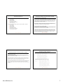
MSP430 Documentation
¾ MSP430 home page (TI)
www.ti.com/msp430
¾ User’s manual
Instructor: Dr Aleksandar Milenkovic
Lecture Note
S18
http://www.ece.uah.edu/~milenka/cpe42104S/manuals/slau049c.pdf
¾ Datasheet
http://www.ece.uah.edu/~milenka/cpe42104S/manuals/slas272c.pdf
¾ TI Workshop document
*Material used is in part developed by
Dr. D. Raskovic and Dr. E. Jovanov
Alex Milenkovich
3
http://www.ece.uah.edu/~milenka/cpe421-04S/manuals/TUTOR.pdf
CPE/EE 421/521 Microcomputers
2
U A H
1
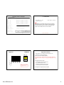
Review: Operating Modes
for Basic Clock System
CPE/EE 421/521 Microcomputers
¾ IAR Workbench Tutorial
U A H
CPE/EE 421/521 Microcomputers
http://www.ece.uah.edu/~milenka/cpe42104S/manuals/430_2002_atc_workshop.pdf
Operating Modes for
Basic Clock System
CPE/EE 421/521 Microcomputers
4
1
The MSP430 family was developed for ultralow-power applications and uses
different levels of operating modes. The MSP430 operating modes, give advanced
support to various requirements for ultralow power and ultralow energy consumption.
This support is combined with an intelligent management of operations during the
U A H
U A H
Operating Modes-General
Low power mode control
There are four bits that control the CPU and the main parts of the operation of the system clock
generator:
CPUOff,
OscOff,
SCG0, and
SCG1.
different module and CPU states. An interrupt event wakes the system from each of
These four bits support discontinuous active mode (AM) requests, to limit the time period of the full
operating mode, and are located in the status register. The major advantage of including the
operating mode bits in the status register is that the present state of the operating condition is
saved onto the stack during an interrupt service request. As long as the stored status register
information is not altered, the processor continues (after RETI) with the same operating mode as
before the interrupt event.
the various operating modes and the RETI instruction returns operation to the mode
that was selected before the interrupt event.
The ultra-low power system design which uses complementary metal-oxide
semiconductor (CMOS) technology, takes into account three different needs:
Minimization of individual current consumption
Limitation of the activity state to the minimum required by the use of low power modes
CPE/EE 421/521 Microcomputers
5
Operating Modes-General
Another program flow may be selected by manipulating the data stored on the stack or the stack
pointer. Being able to access the stack and stack pointer with the instruction set allows the
program structures to be individually optimized, as illustrated in the following program flow:
CPE/EE 421/521 Microcomputers
Enter interrupt routine
Operating Modes - Software configurable
There are six operating modes that the software can configure:
Active mode AM; SCG1=0, SCG0=0, OscOff=0, CPUOff=0: CPU clocks are active
Low power mode 0 (LPM0); SCG1=0, SCG0=0, OscOff=0, CPUOff=1:
CPU is disabled
MCLK is disabled
SMCLK and ACLK remain active
The interrupt routine is entered and processed if an enabled interrupt awakens
the MSP430:
¾
The SR and PC are stored on the stack, with the content present at the interrupt event.
¾
Subsequently, the operation mode control bits OscOff, SCG1, and CPUOff are cleared
automatically in the status register.
Return from interrupt
Two different modes are available to return from the interrupt service routine and continue the flow of
operation:
¾
Return with low-power mode bits set. When returning from the interrupt, the program counter
points to the next instruction. The instruction pointed to is not executed, since the restored low
power mode stops CPU activity.
¾
Return with low-power mode bits reset. When returning from the interrupt, the program
continues at the address following the instruction that set the OscOff or CPUOff-bit in the status
register. To use this mode, the interrupt service routine must reset the OscOff, CPUOff, SCGO,
and SCG1 bits on the stack. Then, when the SR contents are popped from the stack upon RETI,
the operating mode will be active mode (AM).
CPE/EE 421/521 Microcomputers
Alex Milenkovich
6
U A H
The desire for speed and data throughput despite conflicting needs for ultra-low power
U A H
Low power mode 1 (LPM1); SCG1=0, SCG0=1, OscOff=0, CPUOff=1:
CPU is disabled
MCLK is disabled
DCO’s dc generator is disabled if the DCO is not used for MCLK or SMCLK when in active
mode. Otherwise, it remains enabled.
SMCLK and ACLK remain active
Low power mode 2 (LPM2); SCG1=1, SCG0=0, OscOff=0, CPUOff=1:
7
CPU is disabled
MCLK is disabled
SMCLK is disabled
DCO oscillator automatically disabled because it is not needed for MCLK or SMCLK
DCO’s dc-generator remains enabled
ACLK remains active
CPE/EE 421/521 Microcomputers
8
2
Low power mode 3 (LPM3); SCG1=1, SCG0=1, OscOff=0, CPUOff=1:
CPU is disabled
MCLK is disabled
SMCLK is disabled
DCO oscillator is disabled
DCO’s dc-generator is disabled
ACLK remains active
Low power mode 0 or 1 is selected if bit CPUOff in the status register is set. Immediately
after the bit is set the CPU stops operation, and the normal operation of the system core
stops. The operation of the CPU halts and all internal bus activities stop until an interrupt
request or reset occurs. The system clock generator continues operation, and the clock
signals MCLK, SMCLK, and ACLK stay active depending on the state of the other three
status register bits, SCG0, SCG1, and OscOff.
The peripherals are enabled or disabled with their individual control register settings, and
with the module enable registers in the SFRs. All I/O port pins and RAM/registers are
unchanged. Wake up is possible through all enabled interrupts.
Low power mode 4 (LPM4); SCG1=X, SCG0=X, OscOff=1, CPUOff=1:
CPU is disabled
ACLK is disabled
MCLK is disabled
SMCLK is disabled
DCO oscillator is disabled
DCO’s dc-generator is disabled
Crystal oscillator is stopped
CPE/EE 421/521 Microcomputers
Low-Power Modes 2 and 3 (LPM2 and LPM3)
Low-power mode 2 or 3 is selected if bits CPUOff and SCG1 in the status register are set.
Immediately after the bits are set, CPU, MCLK, and SMCLK operations halt and all internal
bus activities stop until an interrupt request or reset occurs.
Peripherals that operate with the MCLK or SMCLK signal are inactive because the clock
signals are inactive. Peripherals that operate with the ACLK signal are active or inactive
according with the individual control registers and the module enable bits in the SFRs. All
I/O port pins and the RAM/registers are unchanged. Wake up is possible by enabled
interrupts coming from active peripherals or RST/NMI.
9
CPE/EE 421/521 Microcomputers
U A H
Operating Modes-Low Power Mode in details
Low-Power Mode 4 (LPM4)
10
U A H
Operating Modes-Low Power Mode in details
Low-Power Mode 0 and 1 (LPM0 and LPM1)
U A H
U A H
Operating Modes #2
Operating Modes-Examples
The following example describes entering into low-power mode 0.
;===Main program flow with switch to CPUOff Mode==============
BIS #18h,SR ;Enter LPM0 + enable general interrupt GIE
;(CPUOff=1, GIE=1). The PC is incremented
System Resets, Interrupts, and Operating Modes In low power mode 4 all activities
cease; only the RAM contents, I/O ports, and registers are maintained. Wake up is only
possible by enabled external interrupts.
;during execution of this instruction and
;points to the consecutive program step.
......
;The program continues here if the CPUOff
;bit is reset during the interrupt service
Before activating LPM4, the software should consider the system conditions during the
low power mode period . The two most important conditions are environmental (that is,
temperature effect on the DCO), and the clocked operation conditions.
;routine. Otherwise, the PC retains its
;value and the processor returns to LPM0.
The following example describes clearing low-power mode 0.
;===Interrupt service routine=================================
The environment defines whether the value of the frequency integrator should be held or
corrected. A correction should be made when ambient conditions are anticipated to
change drastically enough to increase or decrease the system frequency while the device
is in LPM4.
......
BIC #10h,0(SP)
;CPU is active while handling interrupts
;Clears the CPUOff bit in the SR contents
;that were stored on the stack.
RETI
;RETI restores the CPU to the active state
;because the SR values that are stored on
;the stack were manipulated. This occurs
;because the SR is pushed onto the stack
;upon an interrupt, then restored from the
;stack after the RETI instruction.
CPE/EE 421/521 Microcomputers
Alex Milenkovich
11
CPE/EE 421/521 Microcomputers
12
3
C – programming msp430x14x.h
…
/************************
* STATUS REGISTER BITS
#include "In430.h“
************************/
#define C
0x0001
#define Z
0x0002
#define N
0x0004
#define V
0x0100
#define GIE
0x0008
#define CPUOFF
0x0010
#define OSCOFF
0x0020
#define SCG0
0x0040
#define SCG1
0x0080
#define LPM0
_BIS_SR(LPM0_bits)
#define LPM0_EXIT _BIC_SR(LPM0_bits)
#define LPM1
_BIS_SR(LPM1_bits)
#define LPM1_EXIT _BIC_SR(LPM1_bits)
#define LPM2
_BIS_SR(LPM2_bits)
#define LPM2_EXIT _BIC_SR(LPM2_bits)
#define LPM3
_BIS_SR(LPM3_bits)
#define LPM3_EXIT _BIC_SR(LPM3_bits)
#define LPM4
_BIS_SR(LPM4_bits)
#define LPM4_EXIT _BIC_SR(LPM4_bits)
#endif /* End #defines for C */
/*
/*
/*
/*
/*
/*
/*
/*
/*
/*
Enter LP Mode 0 */
Exit LP Mode 0 */
Enter LP Mode 1 */
Exit LP Mode 1 */
Enter LP Mode 2 */
Exit LP Mode 2 */
Enter LP Mode 3 */
Exit LP Mode 3 */
Enter LP Mode 4 */
Exit LP Mode 4 */
QQ?
/* - in430.h Intrinsic functions for the MSP430
*/
CPUOFF
SCG0+CPUOFF
#define LPM2
SCG1+CPUOFF
#define LPM3
SCG1+SCG0+CPUOFF
#define LPM4
SCG1+SCG0+OSCOFF+CPUOFF
// Enter LPM0 w/ interrupt
Your program is in LPM0 mode and it is woke up by an interrupt.
What should be done if you do not want to go back to LPM0 after
servicing the interrupt request, but rather you would let the main
program re-enter LMP0, based on current conditions?
Bits 4-7 in SR */
#define LPM1
....
// program stops here
/* Begin #defines for assembler */
#define LPM0
C Examples
_BIS_SR(LPM0_bits + GIE);
/* Low Power Modes coded with
#ifndef __IAR_SYSTEMS_ICC
U A H
U A H
Operating Modes C Examples
unsigned short _BIS_SR(unsigned short);
unsigned short _BIC_SR(unsigned short);
/* End #defines for assembler */
#else /* Begin #defines for C */
SCG0+CPUOFF
#define LPM2_bits
SCG1+CPUOFF
#define LPM3_bits
SCG1+SCG0+CPUOFF
#define LPM4_bits
SCG1+SCG0+OSCOFF+CPUOFF
13
CPE/EE 421/521 Microcomputers
Digital I/O
all MSP430
Port1
Port2
Port3
…
Port6
Function Select Register PxSEL
yes
yes
Interrupt Edge Select Register PxIES
yes
no
Interrupt Enable Register PxIE
yes
no
Interrupt Flag Register PxIFG
yes
no
Direction Register PxDIR
yes
yes
Output Register PxOUT
yes
yes
yes
yes
Input Register PxIN
14
Digital I/O Introduction
¾ MSP430 family – up to 6 digital I/O ports implemented, P1-P6
¾ MSP430F14x – all 6 ports implemented
Ports P1 and P2 have interrupt capability.
Each interrupt for the P1 and P2 I/O lines can be individually enabled and
configured to provide an interrupt on a rising edge or falling edge of an input
signal.
The digital I/O features include:
P1.
¾ Independently programmable individual I/Os
P2.
P3.
CPE/EE 421/521 Microcomputers
U A H
CPUOFF
#define LPM1_bits
U A H
#define LPM0_bits
7
6
5
4
3
2
1
0
¾ Any combination of input or output
P4.
P5.
P6.
¾ Individually configurable P1 and P2 interrupts
Chapter 9, User’s Manual
pages 9-1 to 9-7
¾ Independent input and output data registers
The digital I/O is configured with user software
CPE/EE 421/521 Microcomputers
Alex Milenkovich
15
CPE/EE 421/521 Microcomputers
16
4
Input Register PnIN
U A H
U A H
Digital I/O Registers Operation
Digital I/O Operation
Direction Registers PnDIR
Each bit in each PnIN register reflects the value of the input signal
at the corresponding I/O pin when the pin is configured as I/O
function.
Do not write to PxIN. It will result
Bit = 0: The input is low
in increased current consumption
Bit = 1: The input is high
Bit = 0: The port pin is switched to input direction
Bit = 1: The port pin is switched to output direction
Function Select Registers PnSEL
Output Registers PnOUT
Port pins are often multiplexed with other peripheral module
functions.
Each bit in each PnOUT register is the value to be output on the
corresponding I/O pin when the pin is configured as I/O function
and output direction.
Bit = 0: I/O Function is selected for the pin
Bit = 1: Peripheral module function is selected for the pin
Bit = 0: The output is low
Bit = 1: The output is high
17
Interrupt Flag Registers P1IFG, P2IFG
(only for P1 and P2)
Bit = 0: No interrupt is pending
C Examples
//***********************************************************
//
MSP-FET430P140 Demo BasicClock Output buffered
//
SMCLK, ACLK and MCLK
//
Description; Output buffered MCLK, SMCLK and ACLK.
//
ACLK = LFXT1 = 32768, MCLK = DCO Max, SMCLK = XT2
//
//** XTAL's REQUIRED - NOT INSTALLED ON FET **//
#include
//
{
WDTCTL = WDTPW +WDTHOLD;
(Only transitions, not static levels, cause interrupts)
Interrupt Edge Select Registers P1IES, P2IES
(only for P1 and P2)
Each PnIES bit selects the interrupt edge for the corresponding I/O pin.
// Stop Watchdog Timer
DCOCTL = DCO0 + DCO1 + DCO2; // Max DCO
MSP430F149
//
<msp430x14x.h>
void main(void)
//
Bit = 1: An interrupt is pending
U A H
Digital I/O Operation
18
CPE/EE 421/521 Microcomputers
U A H
CPE/EE 421/521 Microcomputers
-----------------
BCSCTL1 = RSEL0 + RSEL1 + RSEL2; // XT2on, max RSEL
//
/|\|
//
| |
//
--|RST
XIN|-
//
|
//
|
//
|
//
|RST
//
|
//
|
P5.4|-->MCLK = DCO Max
//
|
P5.5|-->SMCLK = XT2
//
|
P5.6|-->ACLK = 32kHz
| 32k
XOUT||
XT2IN|-
BCSCTL2 |= SELS;
// SMCLK = XT2
P5DIR |= 0x70;
// P5.6,5,4 outputs
P5SEL |= 0x70;
// P5.6,5,5 options
| XTAL (455k - 8Mhz)
while(1)
XT2OUT||
{
}
}
//
Bit = 0: The PnIFGx flag is set with a low-to-high transition
//
M.Buccini
//
Texas Instruments, Inc
Bit = 1: The PnIFGx flag is set with a high-to-low transition
//
January 2004
//
Updated for IAR Embedded Workbench Version: 2.21B
//*************************************************************
CPE/EE 421/521 Microcomputers
Alex Milenkovich
19
CPE/EE 421/521 Microcomputers
20
5
¾ 16-bit counter with 4 operating modes
¾ Selectable and configurable clock source
U A H
U A H
Timer_A MSP430x1xx
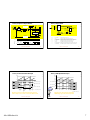
Timer_A5 - MSP430x1xx Block Diagram
¾ Three (or five) independently configurable capture/compare
registers with configurable inputs
¾ Three (or five) individually configurable output modules with 8
output modes
¾ multiple, simultaneous, timings; multiple capture/compares;
multiple output waveforms such as PWM signals; and any
combination of these.
¾ Interrupt capabilities
each capture/compare block individually configurable
Page 11-3, User’s Manual
21
UP/DOWN Mode
Stop/Halt Mode
Timer is halted with the next +CLK
U A H
Timer_A Counting Modes
22
CPE/EE 421/521 Microcomputers
U A H
CPE/EE 421/521 Microcomputers
Timer_A 16-bit Counter
Timer counts between 0 and CCR0 and 0
0FFFFh
UP/DOWN Mode
CCR0
15
0
TACTL
Input
Select
unused
0h
160h
UP Mode
rw(0)
Continuous Mode
Timer counts between 0 and CCR0
rw(0)
rw(0)
rw(0)
rw(0)
rw(0)
rw(0)
rw(0)
rw(0)
Continuous Mode
0FFFFh
CCR0
0h
CPE/EE 421/521 Microcomputers
Alex Milenkovich
rw(0)
Page 11-12, User’s Manual
23
SSEL1 SSEL0
0
0
0
1
1
0
1
1
unTAIE TAIFG
used CLR
Mode
Control
Timer continuously counts up
0FFFFh
0h
Input
Divider
ID1
ID0
0
0
1
1
0
1
0
1
rw(0)
rw(0)
MC1
MC0
0
0
1
1
0
1
0
1
rw(0)
(w)(0)
rw(0)
rw(0)
Stop Mode
Up Mode
Continuous Mode
Up/Down Mode
1/1, Pass
1/2
1/4
1/8
TACLK
ACLK
MCLK
INCLK
CPE/EE 421/521 Microcomputers
24
6
Timer
Clock
CCMx0
0 Disabled
1 Pos. Edge
0 Neg. Edge
1 Both Edges
Synchronize
Capture
CCTLx
162h
to
16Eh
EQU0
15
CAPTURE
MODE
rw(0)
rw(0)
rw(0)
rw(0)
rw(0)
rw(0)
unINPUT
CAP
SCS SCCI
SELECT
used
rw(0)
rw(0)
rw(0)
rw(0)
rw(0)
rw(0)
rw(0)
rw(0)
OUTMODx
rw(0)
rw(0)
rw(0)
rw(0)
rw(0)
rw(0)
Set_CCIFGx
Y
CCIE CCI
rw(0)
r
rw(0)
OMx2 OMx1 OMx0 Function
SCCIx
0
rw(0)
0
OUT COV CCIFG
rw(0)
rw(0)
OUTx
OMx2 OMx1 OMx0
2
rw(0)
Output Signal Outx
Q
POR
Output Mode 0
CAPx
1
EN
A
15
rw(0)
Set
To Output Logic TAx
0
0
rw(0)
D
Comparator
to Port0x
15
rw(0)
Output
Reset
Compare Path
rw(0)
15
OUTx (CCTLx.2)
Logic
SCSx
CCIx
2
TAx
EQUx
Timer Clock
EQUx 0
CCRx
0172h
to
017Eh
Timer Clock
0
Capture/Compare Register
CCRx
Capture
0
Timer_A Output Units
rw(0)
0
0
Output Mode
Outx signal is set according to Outx bit
0
0
1
Set
EQUx sets Outx signal clock synchronous with timer clock
0
1
0
PWM Toggle/Reset
EQUx toggles Outx signal, reset with EQU0, clock sync. with timer clock
0
1
1
PWM Set/Reset
EQUx sets Outx signal, reset with EQU0, clock synchronous with timer clock
1
0
0
Toggle
EQUx toggles Outx signal, clock synchronous with timer clock
1
0
1
Reset
EQUx resets Outx signal clock synchronous with timer clock
1
1
0
PWM Toggle/Reset
EQUx toggles Outx signal, set with EQU0, clock synchronous with timer clock
1
1
1
PWM Set/Reset
EQUx resets Outx signal, set with EQU0, clock synchronous with timer clock
25
Timer_A Continuous-Mode Example
0FFFh
26
CPE/EE 421/521 Microcomputers
U A H
CPE/EE 421/521 Microcomputers
Operational Conditions
0
U A H
CCMx1
0
0
1
1
15
1
Capture
Mode
Timer Bus
Data Bus
U A H
Capture Path
CMPx
CCISx1 CCISx0
0
1
2
3
CCIxA
CCIxB
GND
VCC
Overflow x
COVx
Logic
U A H
Timer_A Capture Compare Blocks
Timer_A PWM Up-Mode Example
0FFFFh
CCR0
CCR1
0h
Px.x
CCR2
0h
CCR0:
Capture Mode: Positive Edge
TA0 Input
TA1 Output
CCR1: PWM Set/Reset
Px.y
TA1 Input
Px.z
TA2 Input
CCR1:
Capture Mode: Both Edges
Px.x
TA2 Output
CCR2: PWM Reset/Set
Px.y
CCR2:
Capture Mode: Negative Edge
CCR0
CCR0: PWM Toggle
CCR0
CCR1 CCR1
CCR1
CCR1
CCR1 CCR1
Interrupts can be generated
Auto
Re-load
TA0 Output
Px.z
EQU0
EQU2
EQU1
EQU0
EQU2
EQU1
EQU2
EQU0
Interrupts can be generated
CCR2
Output Mode 4: PWM Toggle
Example shows three different asymmetric
PWM-Timings generated with the Up-Mode
Example shows three independent HW event captures.
CCRx “stamps” time of event - Continuous-Mode is ideal.
CPE/EE 421/521 Microcomputers
Alex Milenkovich
27
CPE/EE 421/521 Microcomputers
28
7
thlfper
CCR0
CCR2
CCR1
CCR3
0h
TA1 Output
0 Degrees
(0.5xVmotor)
tpw2
TA0 Output
Px.z
(0.07xVmotor)
TIMOV
EQU0
TIMOV
EQU0
TIMOV
MSP-FET430P140 Demo - Timer_A Toggle P1.0,
#include <msp430x14x.h>
//
CCR0 Contmode ISR, DCO SMCLK
//
Description; Toggle P1.0 using software and TA_0 ISR. Toggle rate is
void main(void)
//
set at 50000 DCO/SMCLK cycles. Default DCO frequency used for TACLK.
{
//
Durring the TA_0 ISR P0.1 is toggled and 50000 clock cycles are
added to
//
CCR0. TA_0 ISR is triggered exactly 50000 cycles. CPU is normally
off and
//
used only durring TA_ISR.
//
ACLK = n/a, MCLK = SMCLK = TACLK = DCO~ 800k
//
Px.y
tpw3
-120 Degrees
//
WDTCTL = WDTPW + WDTHOLD;
// Stop WDT
P1DIR |= 0x01;
// P1.0 output
CCTL0 = CCIE;
// CCR0 interrupt enabled
CCR0 = 50000;
TACTL = TASSEL_2 + MC_2; // SMCLK, contmode
//
TA2 Output
(0.93xVmotor)
//***************************************************************
//
tpw1
+120 Degrees
C Examples
//
Px.x
U A H
U A H
Timer_A PWM Up/Down Mode Example
0FFFFh
MSP430F149
_BIS_SR(LPM0_bits + GIE); // Enter LPM0 w/ interrupt
---------------
//
/|\|
//
| |
//
--|RST
//
|
//
|
}
XIN||
XOUT|-
// Timer A0 interrupt service routine
|
interrupt[TIMERA0_VECTOR] void TimerA(void)
P1.0|-->LED
{
//
Interrupts can be generated
Example shows Symmetric PWM Generation Digital Motor Control
P1OUT ^= 0x01; // Toggle P1.0
//
M. Buccini
//
Texas Instruments, Inc
//
September 2003
//
Built with IAR Embedded Workbench Version: 1.26B
//
December 2003
//
Updated for IAR Embedded Workbench Version: 2.21B
CCR0 += 50000; // Add Offset to CCR0
}
//**********************************************************************
CPE/EE 421/521 Microcomputers
Alex Milenkovich
29
CPE/EE 421/521 Microcomputers
30
8