1
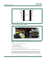
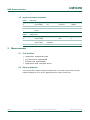
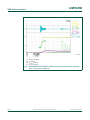
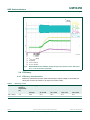
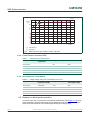
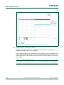
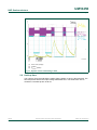
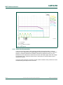
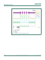
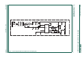
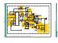
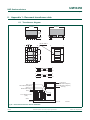
UM10450
TEA1713 demo board for 90 W notebook adapter
Rev. 1 — 11 April 2011
User manual
Document information
Info
Content
Keywords
TEA1713T, 90 W, notebook adapter, LLC, resonant, half-bridge, PFC,
controller, converter, burst mode, power supply, demo board.
Abstract
The TEA1713T includes a Power Factor Correction (PFC) controller as
well as a controller for a Half-Bridge resonant Converter (HBC).
This user manual describes a 90 W resonant switching mode power
supply for a typical notebook adapter design based on the TEA1713T. The
board provides an output of 19.5 V/4.65 A. It operates in normal mode for
medium and high power levels and in burst mode for low power levels.
Burst mode operation provides a reduction of power losses to increase
performance.
The efficiency at high power is well above 90 % and the no load power
consumption is well below 500 mW.
UM10450
NXP Semiconductors
TEA1713 demo board for 90 W notebook adapter
Revision history
Rev
Date
Description
v.1
20110411
first release
UM10450
User manual
All information provided in this document is subject to legal disclaimers.
Rev. 1 — 11 April 2011
© NXP B.V. 2011. All rights reserved.
2 of 38
UM10450
NXP Semiconductors
TEA1713 demo board for 90 W notebook adapter
1. Introduction
1.1 Scope of this document
This document describes the 90 W notebook adapter demo board using the TEA1713T. A
functional description is provided, supported by a set of measurements to show the
notebook adapter characteristics.
WARNING
Lethal voltage and fire ignition hazard
The non-insulated high voltages that are present when operating this product, constitute a
risk of electric shock, personal injury, death and/or ignition of fire.
This product is intended for evaluation purposes only. It shall be operated in a designated test
area by personnel qualified according to local requirements and labor laws to work with
non-insulated mains voltages and high-voltage circuits. This product shall never be operated
unattended.
1.2 TEA1713T
The TEA1713T integrates a controller for PFC and a controller for a HBC. It provides the
drive function for the discrete MOSFET of the up-converter and for the two discrete power
MOSFETs in a resonant half-bridge configuration.
The resonant controller part is a high voltage controller for a Zero Voltage Switching (ZVS)
LLC resonant converter. It includes a high voltage level shift circuit and several protection
features such as OverCurrent Protection (OCP), Open-Loop Protection (OLP), Capacitive
Mode Protection (CMP) and a general purpose latched protection input.
In addition to the resonant controller, the TEA1713T contains a PFC controller. The
efficient operation of the PFC is obtained by functions such as quasi-resonant operation at
high power levels and quasi-resonant operation with valley skipping at lower power levels.
OCP, OverVoltage Protection (OVP) and demagnetization sensing, ensures safe
operation in all conditions.
The proprietary high voltage BCD power logic process makes direct start-up from the
rectified universal mains voltage in an efficient way possible. A second low voltage
Silicon-On-Insulator (SOI) IC is used for accurate, hi-speed protection functions and
control.
The combination of PFC and a resonant controller in one IC makes the TEA1713T very
suitable for notebook adapters.
UM10450
User manual
All information provided in this document is subject to legal disclaimers.
Rev. 1 — 11 April 2011
© NXP B.V. 2011. All rights reserved.
3 of 38
UM10450
NXP Semiconductors
TEA1713 demo board for 90 W notebook adapter
COMPPFC
1
24 SNSBOOST
SNSMAINS
2
23 RCPROT
SNSAUXPFC
3
22 SSHBC/EN
SNSCURPFC
4
21 SNSFB
SNSOUT
5
20 RFMAX
SUPIC
6
GATEPFC
7
PGND
8
17 SNSCURHBC
SUPREG
9
16 n.c.
GATELS 10
15 HB
TEA1713T
19 CFMIN
18 SGND
14 SUPHS
n.c. 11
13 GATEHS
SUPHV 12
014aaa826
Fig 1.
Pin configuration TEA1713T
1.3 Setup of the 90 W notebook adapter
019aab663
Fig 2.
TEA1713T demo board 90 W notebook adapter
The board can operate at a mains input voltage of between 90 V and 264 V (universal
mains).
The demo board contains two sub-circuits:
• A PFC of BCM-type
• A HBC of resonant LLC-type
Both converters are controlled by the TEA1713T.
At low power levels, the converters operate in burst mode to reduce power losses.
The purpose of the demo board is to demonstrate the operation of the TEA1713T in a
single output supply including burst mode operation. The performance is according
today’s general standards and can be used as a starting point for further development.
UM10450
User manual
All information provided in this document is subject to legal disclaimers.
Rev. 1 — 11 April 2011
© NXP B.V. 2011. All rights reserved.
4 of 38
UM10450
NXP Semiconductors
TEA1713 demo board for 90 W notebook adapter
1.4 Input and output properties
Table 1.
Input data
Symbol
Description
Conditions
Specification
Unit
Vi
input voltage
AC
90 to 264
V (RMS)
fi
input frequency
-
47 to 60
Hz
Pi(no load)
no load input
power
230 V, 50 Hz
< 500
mW
Table 2.
Output data
Symbol
Description
Conditions
Specification
Unit
Vo
output voltage
-
19.5
V
Vo(ripple)(p-p)
peak-to-peak
ripple voltage
20 MHz
bandwidth
< 150
mV
Io
output current
continuous
0 to 4.65
A
2. Measurements
2.1 Test facilities
•
•
•
•
Oscilloscope: Yokogawa DL1640L
AC power source: Agilent 6812B
Electronic load: Agilent 6063B
Digital power meter: Yokogawa WT210
2.2 Start-up behavior
The rise time of the output voltage (measured from 10 % to 90 % point of the nominal
output) is between 3 ms to 15 ms, depending on the output current load.
UM10450
User manual
All information provided in this document is subject to legal disclaimers.
Rev. 1 — 11 April 2011
© NXP B.V. 2011. All rights reserved.
5 of 38
UM10450
NXP Semiconductors
TEA1713 demo board for 90 W notebook adapter
(1)
(2)
(3)
(4)
019aab664
(1) PFC (Yellow)
(2) HBC (Green)
(3) VO (Purple)
(4) IO (Blue)
Fig 3.
UM10450
User manual
Start-up behavior at Vmains = 230 V and no load
All information provided in this document is subject to legal disclaimers.
Rev. 1 — 11 April 2011
© NXP B.V. 2011. All rights reserved.
6 of 38
UM10450
NXP Semiconductors
TEA1713 demo board for 90 W notebook adapter
(1)
(2)
(3)
(4)
019aab665
(1) PFC (Yellow)
(2) HBC (Green)
(3) VO (Purple)
(4) IO (Blue)
Fig 4.
Start-up behavior at Vmains = 100 V and full load
2.3 Protection levels on SNSCURHBC and SNSOUT during start-up
During start-up the voltage at pin RCPROT (protection timer) always rises. SNSCURHBC
detects the initial high primary current and SNSOUT starts at a low voltage. After the first
switching cycles the levels become normal for operation and the charging of RCPROT
ends. The voltage level on RCPROT now decreases to zero again by the external
discharge resistor that is part of the RCPROT system. During normal start-up the initial
charging of RCPROT must not trigger a protection (4 V level).
UM10450
User manual
All information provided in this document is subject to legal disclaimers.
Rev. 1 — 11 April 2011
© NXP B.V. 2011. All rights reserved.
7 of 38
UM10450
NXP Semiconductors
TEA1713 demo board for 90 W notebook adapter
(1)
(2)
(3)
(4)
019aab666
(1) VSNSCURHBC (Blue)
(2) VO (Yellow)
(3) VSNSOUT (Green)
(4) VRCPROT (Purple)
Fig 5.
UM10450
User manual
SNSCURHBC and/or SNSOUT initially charges the protection timer. Start-up at
Vmains = 230 V and no load (0 A)
All information provided in this document is subject to legal disclaimers.
Rev. 1 — 11 April 2011
© NXP B.V. 2011. All rights reserved.
8 of 38
UM10450
NXP Semiconductors
TEA1713 demo board for 90 W notebook adapter
(1)
(2)
(3)
(4)
019aab667
(1) VSNSCURHBC (Blue)
(2) VO (Yellow)
(3) VSNSOUT (Green)
(4) VRCPROT (Purple)
Fig 6.
SNSCURHBC and/or SNSOUT initially charges the protection timer. Start-up at
Vmains = 100 V and full load (4.65 A)
2.4 Efficiency
2.4.1 Efficiency characteristics
Efficiency measurements were made measuring the output voltage on the board (not
taking into account the losses in an output connection cable).
Table 3.
Efficiency results
Conditions
Energy star 2.0 Efficiency (%)
efficiency
requirement
(%)
Average
25 % load
50 % load
75 % load
100 % load
100 V, 60 Hz
> 87
90.0
87.5
90.4
91.1
91.1
230 V, 50 Hz
> 87
91.2
88.1
91.5
92.6
92.5
UM10450
User manual
All information provided in this document is subject to legal disclaimers.
Rev. 1 — 11 April 2011
© NXP B.V. 2011. All rights reserved.
9 of 38
UM10450
NXP Semiconductors
TEA1713 demo board for 90 W notebook adapter
019aab668
100
(1)
efficiency
(%)
80
(2)
60
40
20
0
0
20
40
60
80
100
Po (W)
(1) Input of 230 V
(2) Input 100 V
Fig 7.
Efficiency at an input voltage of 100 V and 230 V
2.4.2 Power Factor Correction (PFC)
Table 4.
Power Factor correction (PFC)
Condition
Energy Star 2.0
requirement
Output power (W)
Power factor
90 V, 60 Hz
-
90
0.99
100 V, 60 Hz
-
90
0.99
115 V, 60 Hz
≥ 0.9
90
0.98
230 V, 50 Hz
-
90
0.91
264 V, 50 Hz
-
90
0.89
2.4.3 No load power consumption
Table 5.
Output voltage and power consumption at no load
Condition
Energy Star 2.0
requirement (mW)
Output voltage (V)
No load power
consumption (mW)
90 V, 60 Hz
≤ 500 mW
19.5
340
100 V, 60 Hz
≤ 500 mW
19.5
340
115 V, 60 Hz
≤ 500 mW
19.5
340
230 V, 50 Hz
≤ 500 mW
19.5
380
264 V, 50 Hz
≤ 500 mW
19.5
385
2.5 Behavior in burst mode operation
In order to reach the no load power consumption requirements (seeSection 2.4.3), burst
mode operation is implemented to improve the performance at low output load. For the
demo board burst mode is active below approximately 5 W output power.
UM10450
User manual
All information provided in this document is subject to legal disclaimers.
Rev. 1 — 11 April 2011
© NXP B.V. 2011. All rights reserved.
10 of 38
UM10450
NXP Semiconductors
TEA1713 demo board for 90 W notebook adapter
019aab669
10
Pin - Pout
(W)
8
6
(2)
(3)
4
2
(1)
0
0
20
40
60
80
100
Po (W)
(1) Burst mode operation
(2) Vmains = 100 V
(3) Vmains = 230 V
Fig 8.
Reduction of power losses as a function of output power
(1)
(2)
(3)
019aab670
(1) VSNSFB (Blue)
(2) VO (Purple)
(3) HBC (Green)
Fig 9.
UM10450
User manual
Burst mode operation at Vmains = 230 V and no load
All information provided in this document is subject to legal disclaimers.
Rev. 1 — 11 April 2011
© NXP B.V. 2011. All rights reserved.
11 of 38
UM10450
NXP Semiconductors
TEA1713 demo board for 90 W notebook adapter
(1)
(2)
(3)
019aab671
(1) PFC (Yellow)
(2) HBC (Green)
(3) VSNSOUT (Blue)
Fig 10. Switch on/off PFC and HBC by VSNSOUT in burst mode operation
The interruptive character of burst mode can lead to the generation of unwanted audible
noise. As the supply in burst mode only operates at low power levels, audible noise levels
are low.
2.6 Transient response
Normal load transients lead to a ripple on the output voltage of < 550 mV.
UM10450
User manual
All information provided in this document is subject to legal disclaimers.
Rev. 1 — 11 April 2011
© NXP B.V. 2011. All rights reserved.
12 of 38
UM10450
NXP Semiconductors
TEA1713 demo board for 90 W notebook adapter
(1)
(2)
019aab672
(1) VO (Purple)
(2) IO (Blue)
Fig 11. Load-step behavior. Typical load-step from zero to full load
2.7 Output ripple voltage and noise
Ripple and noise are measured at full output load, buffered with a 10 μF capacitor in
parallel with a high-frequency 0.1 μF capacitor.
The varying input voltage of the resonant converter causes a frequency component in the
output ripple voltage that is related to the mains voltage frequency: 50 Hz or 60 Hz. The
switching frequency of the resonant converter causes the other component in the output
ripple voltage.
Table 6.
UM10450
User manual
Ripple and noise test results
Mains voltage
Mains frequency Output power
Ripple frequency Voltage ripple
90 V to 264 V
50 Hz or 60 Hz
90 W
50 Hz or 60 Hz
23 mV (p-p)
90 V to 264 V
50 Hz or 60 Hz
90 W
75 kHz
125 mV (p-p)
All information provided in this document is subject to legal disclaimers.
Rev. 1 — 11 April 2011
© NXP B.V. 2011. All rights reserved.
13 of 38
UM10450
NXP Semiconductors
TEA1713 demo board for 90 W notebook adapter
(1)
(2)
(3)
019aab674
(1) VO (Yellow)
(2) VO (Purple)
(3) IO (Blue)
Fig 12. Output voltage ripple at full load (2 ms/div scale)
UM10450
User manual
All information provided in this document is subject to legal disclaimers.
Rev. 1 — 11 April 2011
© NXP B.V. 2011. All rights reserved.
14 of 38
UM10450
NXP Semiconductors
TEA1713 demo board for 90 W notebook adapter
(1)
(2)
(3)
019aab675
(1) VO (Yellow)
(2) VO (Purple)
(3) IO (Blue)
Fig 13. Output voltage ripple at full load (20 μs/div scale)
2.8 OverPower Protection (OPP)
Tested with a higher current (dynamic overload) on the output voltage, the OPP is
activated when the current exceeds 6 A (117 W). This corresponds to a load condition that
is 30 % higher than the rated power for continuous use. The OPP is detected by the
SNSCURHBC function of the TEA1713T that monitors the primary resonant current.
When the voltage on the SNSCURHBC pin exceeds 0.5 V (or −0.5 V) the protection timer
is started.
UM10450
User manual
All information provided in this document is subject to legal disclaimers.
Rev. 1 — 11 April 2011
© NXP B.V. 2011. All rights reserved.
15 of 38
UM10450
NXP Semiconductors
TEA1713 demo board for 90 W notebook adapter
(1)
(2)
(3)
019aab676
(1) VSNSCURHBC (Purple)
(2) IO (Blue)
(3) VRCPROT (Yellow)
Fig 14. Dynamic current load leading to OPP
2.9 Hold-up time
The output is set to full load and the mains supply voltage of 100 V is disconnected. The
time that passes before the output voltage falls below 90 % of its initial value is then
measured. The hold-up time is 28 ms.
UM10450
User manual
All information provided in this document is subject to legal disclaimers.
Rev. 1 — 11 April 2011
© NXP B.V. 2011. All rights reserved.
16 of 38
UM10450
NXP Semiconductors
TEA1713 demo board for 90 W notebook adapter
(1)
(2)
(3)
019aab677
(1) VO (Purple)
(2) IO (Blue)
(3) Vmains (Green and Yellow)
Fig 15. Hold-up time
2.10 Short-circuit protection
A short circuit on the output of the resonant converter causes the primary current to
increase. This is detected by the SNSCURHBC function leading to running on maximum
frequency until the protection timer RCPROT reaches its protection level (4 V). The
RCPROT function performs its restart timer function and restarts again when the voltage
has dropped to 0.5 V. When the short-circuit is removed, the converter starts up and
operates as normal.
This is the main protection mechanism. Under certain conditions other protections can be
activated during the output short circuit test.
UM10450
User manual
All information provided in this document is subject to legal disclaimers.
Rev. 1 — 11 April 2011
© NXP B.V. 2011. All rights reserved.
17 of 38
UM10450
NXP Semiconductors
TEA1713 demo board for 90 W notebook adapter
(1)
(2)
(3)
(4)
019aab678
(1) VSNSCURHBC (Purple)
(2) VRCPROT (Yellow)
(3) IO (Blue)
(4) VO (Green)
Fig 16. Protection and restart at output short-circuit
UM10450
User manual
All information provided in this document is subject to legal disclaimers.
Rev. 1 — 11 April 2011
© NXP B.V. 2011. All rights reserved.
18 of 38
UM10450
NXP Semiconductors
TEA1713 demo board for 90 W notebook adapter
2.11 Resonant current measurements
(1)
(2)
(3)
(4)
019aab679
(1) Iresonant_primary (Blue)
(2) VCFMIN (Yellow)
(3) VHB Green)
(4) VGATE_MOSFET_LS (Purple)
Fig 17. Resonant current (full load IO = 4.65 A)
UM10450
User manual
All information provided in this document is subject to legal disclaimers.
Rev. 1 — 11 April 2011
© NXP B.V. 2011. All rights reserved.
19 of 38
UM10450
NXP Semiconductors
TEA1713 demo board for 90 W notebook adapter
(1)
(2)
(3)
(4)
019aab680
(1) Iresonant_primary (Blue)
(2) VCFMIN (Yellow)
(3) VHB (Green)
(4) VGATE_MOSFET_LS (Purple)
Fig 18. Resonant current (low load IO = 0.5 A)
UM10450
User manual
All information provided in this document is subject to legal disclaimers.
Rev. 1 — 11 April 2011
© NXP B.V. 2011. All rights reserved.
20 of 38
UM10450
NXP Semiconductors
TEA1713 demo board for 90 W notebook adapter
(1)
(2)
(3)
(4)
019aab681
(1) Iresonant_primary (Blue)
(2) VCFMIN (Yellow)
(3) VHB (Green)
(4) VGATE_MOSFET_LS (Purple)
Fig 19. Resonant current (no load IO = 0 A)
UM10450
User manual
All information provided in this document is subject to legal disclaimers.
Rev. 1 — 11 April 2011
© NXP B.V. 2011. All rights reserved.
21 of 38
UM10450
NXP Semiconductors
TEA1713 demo board for 90 W notebook adapter
2.12 Temperature measurement
Sp1 57.5
Sp8 58.5
Sp7 55.6
Sp6 57.4
Sp2 66.3
Sp10 59.7
Sp3 63.9
Sp9 54.8
Sp4 67.1
Sp5 68.3
019aab682
Fig 20. Temperature overview at full load and mains supply of 115 V
2.13 EMI performance
Conditions:
•
•
•
•
•
•
UM10450
User manual
Type: Conducted EMC measurement
Frequency range: 150 kHz to 30 MHz
Output power: Full load condition
Supply voltage: 115 V and 230 V
Measuring time: 50 ms
Secondary ground connected to mains earth ground
All information provided in this document is subject to legal disclaimers.
Rev. 1 — 11 April 2011
© NXP B.V. 2011. All rights reserved.
22 of 38
xxxx xxxxxxxxxxxxxxxxxxxxxxxxxxxxxx x xxxxxxxxxxxxxx xxxxxxxxxx xxx xxxxxx xxxxxxxxxxxxxxxxxxxxxxx xxxxxxxxxxxxxxxxxxxxxx
xxxxx xxxxxx xx xxxxxxxxxxxxxxxxxxxxxxxxxxxxx xxxxxxxxxxxxxxxxxxxxxx xxxxxxxxxxx xxxxxxx xxxxxxxxxxxxxxxxxxx
xxxxxxxxxxxxxxxx xxxxxxxxxxxxxx xxxxxx xx xxxxxxxxxxxxxxxxxxxxxxxxxxxxxxxx xxxxxxxxxxxxxxxxxxxxxxxx xxxxxxx
xxxxxxxxxxxxxxxxxxxxxxxxxxxxxxxxxxxxxxxxxxxxxx xxxxxxxxxxx xxxxx x x
L101
G
VF101
2K471
1 mH
1A
C101
330 nF
275 V
R101
2 MΩ
R102
2 MΩ
MUR460
R103
5.1 kΩ
12.8 mH
R134
R108
3.6 kΩ
R133
47 kΩ
C120
2 μF
R113
0Ω
U101 (PART)
SNSAUXPFC
560 kΩ
SNSMAINSPFC
3
12
2
7
C121
2 μF
GATEPFC
R132
COMPPFC
33 kΩ
8
1
C107
100 pF
R104
10 Ω
D108
TEA1713
PGND
Q100
2SK3568
SUPHV
(PART)
C122
470 nF
E101
68 μF
450 V
VBUS
C106
470 nF
N
CN101
VBUS
220 μH
C104
470 nF
L102
D102
40TS:2Ts
L104
L103
BD101
GBU806
R105
100 kΩ
R110
4.7 MΩ
BAS316
4
24
SNSCURPFC R107
R106
1 kΩ
12 kΩ
C108
SNSBOOST
R109
4.7 MΩ
R112
0.1 Ω
1W
R111A
3.6 kΩ
47 nF
C123
150 nF
C109
4.7 nF
R111B
56 kΩ
019aab798
UM10450
23 of 38
© NXP B.V. 2011. All rights reserved.
Fig 21. Circuit diagram TEA1713T 90 W demo board (PFC part)
TEA1713 demo board for 90 W notebook adapter
Rev. 1 — 11 April 2011
All information provided in this document is subject to legal disclaimers.
3.15 A
250 V
NXP Semiconductors
3. Circuit diagram
UM10450
User manual
F101
L
xxxx xxxxxxxxxxxxxxxxxxxxxxxxxxxxxx x xxxxxxxxxxxxxx xxxxxxxxxx xxx xxxxxx xxxxxxxxxxxxxxxxxxxxxxx xxxxxxxxxxxxxxxxxxxxxx
xxxxx xxxxxx xx xxxxxxxxxxxxxxxxxxxxxxxxxxxxx xxxxxxxxxxxxxxxxxxxxxx xxxxxxxxxxx xxxxxxx xxxxxxxxxxxxxxxxxxx
xxxxxxxxxxxxxxxx xxxxxxxxxxxxxx xxxxxx xx xxxxxxxxxxxxxxxxxxxxxxxxxxxxxxxx xxxxxxxxxxxxxxxxxxxxxxxx xxxxxxx
xxxxxxxxxxxxxxxxxxxxxxxxxxxxxxxxxxxxxxxxxxxxxx xxxxxxxxxxx xxxxx x x
NXP Semiconductors
UM10450
User manual
D103
Q102
SPA04N60C3
BAS316
R114
R115
10 Ω
22 Ω
VBUS
C110
47 pF
U101
GATEHS
D107
MURS160
C117
330 nF
14
11
15
10
SUPHV
SNSCURHB
16
9
17
8
BAS316
GATELS
R118
R116
10 Ω
22 Ω
18
7
C111
47 pF
R144
C112
1 nF
C132
680 nF
PGND
E103
4.7 μF
SNSCURHB
SUPREG
GATEPFC
C124
R131
RFMAX
19
6
20
5
SUPIC
C118
680 nF
SNSOUT
18 kΩ
SNSFB
C105
C125
220 nF
C126
2.2 μF
RCPROT
R130
75 kΩ
4
R117
10 Ω
E102
220 μF
C116
10 nF
SNSCURPFC
R119
D105
0Ω
BAS316
270 kΩ
R121
39 kΩ
SNSBOOST
3
SUPREG
23
2
24
1
SNSMAINS
U102A
LM393D
1
Q104
BC847-40
8 2
4 3
COMPPFC
R128
R135A
7
R124
33 kΩ
R125
56 kΩ
n.m.
n.m.
R135B
n.m.
C119
10 nF
C129
6.8 nF
R126
2.2 kΩ
R138
470 Ω
R125A
3 kΩ
100 kΩ
U102B
LM393D
soldering
output cable
D110
MBR2060
SNSAUXPFC
R122
33 kΩ
19V_4.72A
E107
470 μF
C115 BAS316
390 nF
C130
22
n.m.
E106
470 μF
D106
R120
n.m.
R143
C114
2.2 nF
n.m.
SSHBC/EN
EN
21
D109
MBR2060
D110
BAV99
SUPIC
330 pF
C131
C113
22 nF
n.m.
TEA1713
CFMIN
Lp = 1.4 mH
Ls = 196 μH
50 : 6 : 5 : 5
(Prim:Aux:Sec1:Sec2)
SUPREG
1 kΩ
SGND
T101
Q103
SPA04N60C3
n.c.
6
C103
1 nF
U106
SFH615A-2
CTR 63 % - 128 %
SUPREG
R146
330 Ω
R141
C134
R139
15 kΩ
1%
2.7 kΩ
47 nF
C133
5
2.2 nF
R127
C128
0Ω
2.2 nF
U105
TL431
R140A
0Ω
019aab683
Fig 22. Circuit diagram TEA1713T 90 W demo board (HBC part)
UM10450
24 of 38
© NXP B.V. 2011. All rights reserved.
R140B
2.2 kΩ
1%
TEA1713 demo board for 90 W notebook adapter
Rev. 1 — 11 April 2011
All information provided in this document is subject to legal disclaimers.
HB
n.c.
R123
12
D104
SUPHS
SUPREG
SNSCURHB
13
xxxx xxxxxxxxxxxxxxxxxxxxxxxxxxxxxx x xxxxxxxxxxxxxx xxxxxxxxxx xxx xxxxxx xxxxxxxxxxxxxxxxxxxxxxx xxxxxxxxxxxxxxxxxxxxxx
xxxxx xxxxxx xx xxxxxxxxxxxxxxxxxxxxxxxxxxxxx xxxxxxxxxxxxxxxxxxxxxx xxxxxxxxxxx xxxxxxx xxxxxxxxxxxxxxxxxxx
xxxxxxxxxxxxxxxx xxxxxxxxxxxxxx xxxxxx xx xxxxxxxxxxxxxxxxxxxxxxxxxxxxxxxx xxxxxxxxxxxxxxxxxxxxxxxx xxxxxxx
xxxxxxxxxxxxxxxxxxxxxxxxxxxxxxxxxxxxxxxxxxxxxx xxxxxxxxxxx xxxxx x x
NXP Semiconductors
UM10450
User manual
3.15 A
250 V
L101
G
VF101
2K471
1 mH
1A
C101
330 nF
275 V
R101
2 MΩ
R102
2 MΩ
MUR460
COIL STATE
SENSING
C106
470 nF
R103
5.1 kΩ
12.8 mH
R134
PFC FILTER
MAINS INPUT FILERS
VBUS
R113
0Ω
U101 (PART)
SNSAUXPFC
N
CN101
VBUS
220 μH
C104
470 nF
L102
D102
40TS:2Ts
L104
L103
BD101
GBU806
3
12
3.6 kΩ
R108
SNSMAINSPFC
560 kΩ
R133
47 kΩ
C120
2 μF
C121
2 μF
TEA1713
(PART)
SENSING MAINS VOLTAGE
PGND
PRESET OF GAIN
COMPENSATION FOR
MAINS VOLTAGE
R132
COMPPFC
33 kΩ
C122
470 nF
7
2
C123
150 nF
8
4
1
24
SUPHV
HIGH
VOLTAGE
STARTUP
GATEPFC
R104
OPTIONAL
CIRCUIT TO
LIMIT GATE
DRIVE CURRENT
10 Ω
D108
SNSCURPFC
SNSBOOST
E101
68 μF
450 V
BUS
VOLTAGE
SENSING
Q100
2SK3568
C107
100 pF
R105
100 kΩ
R110
4.7 MΩ
BAS316
R107
R106
1 kΩ
12 kΩ
C108
R109
4.7 MΩ
R112
0.1 Ω
1W
R111A
3.6 kΩ
47 nF
CURRENT SENSING AND
SOFT-START PRESET
C109
4.7 nF
R111B
56 kΩ
019aab799
UM10450
25 of 38
© NXP B.V. 2011. All rights reserved.
Fig 23. Circuit diagram TEA1713T 90 W demo board with comments (PFC part)
TEA1713 demo board for 90 W notebook adapter
Rev. 1 — 11 April 2011
All information provided in this document is subject to legal disclaimers.
F101
L
xxxx xxxxxxxxxxxxxxxxxxxxxxxxxxxxxx x xxxxxxxxxxxxxx xxxxxxxxxx xxx xxxxxx xxxxxxxxxxxxxxxxxxxxxxx xxxxxxxxxxxxxxxxxxxxxx
xxxxx xxxxxx xx xxxxxxxxxxxxxxxxxxxxxxxxxxxxx xxxxxxxxxxxxxxxxxxxxxx xxxxxxxxxxx xxxxxxx xxxxxxxxxxxxxxxxxxx
xxxxxxxxxxxxxxxx xxxxxxxxxxxxxx xxxxxx xx xxxxxxxxxxxxxxxxxxxxxxxxxxxxxxxx xxxxxxxxxxxxxxxxxxxxxxxx xxxxxxx
xxxxxxxxxxxxxxxxxxxxxxxxxxxxxxxxxxxxxxxxxxxxxx xxxxxxxxxxx xxxxx x x
NXP Semiconductors
UM10450
User manual
D103
Q102
SPA04N60C3
BAS316
R114
R115
10 Ω
22 Ω
VBUS
OPTIONAL
C110 CAPACITORS
47 pF TO OPTIMIZE
OPTIONAL CIRCUIT TO LIMIT
GATE DRIVE CURRENT
U101
GATEHS
D107
MURS160
C117
330 nF
14
11
OPTIONAL CIRCUIT
SUPHV TO LIMIT GATE
DRIVE CURRENT
HB
n.c.
SNSCURHB
15
10
16
9
17
8
BAS316
GATELS
R118
R116
10 Ω
22 Ω
OPTIONAL COMPENSATION
OF OCR+OCP FOR INPUT
VOLTAGE VARIATIONS
SGND
E103
4.7 μF
C132
680 nF
6
RFMAX
20
5
21
4
SNSOUT
C118
680 nF
C105
n.m.
SSHBC/EN
C125
220 nF
C126
2.2 μF
RCPROT
R130
75 kΩ
SNSBOOST
22
3
23
2
24
1
n.m.
SNSAUXPFC
E102
220 μF
TIMING PFC
BURST
R119
D105
0Ω
BAS316
270 kΩ
R121
39 kΩ
Q104
BC847-40
E106
470 μF
8 2
4 3
COMPPFC
R128
BURST MODE
COMPARATOR
CIRCUIT
7
soldering
output cable
R124
33 kΩ
R125
56 kΩ
R135A
C130
n.m.
n.m.
R135B
OPTIONAL CIRCUIT
TO OPTIMIZE DIODE
SWITCHING
n.m.
C119
10 nF
C129
6.8 nF
R126
2.2 kΩ
OUTPUT VOLTAGE SENSING AND REGULATION
WITH A TYPICAL TL431 AND OPTOCOUPLER
CONSTRUCTION
R138
470 Ω
R125A
3 kΩ
100 kΩ
U102B
LM393D
19V_4.72A
E107
470 μF
D110
MBR2060
MEASURING OUTPUT
VOLTAGE ON OVP AND UVP
1
n.m.
C115 BAS316
390 nF
SUPREG
U102A
LM393D
OPTIONAL CIRCUIT
TO OPTIMIZE DIODE
SWITCHING
C114
2.2 nF
D106
R120
R122
33 kΩ
SNSMAINS
R117
10 Ω
DISABLING OCP FUNCTION
(OCR REMAINS)
C116
10 nF
SNSCURPFC
n.m.
R143
D109
MBR2060
D110
BAV99
SUPIC
18 kΩ
EN
PRESET OF
RC-TIMER
GATEPFC
C131
C113
22 nF
SNSCURHB
SUPREG
SUPIC
19
R144
C112
1 nF
PGND
330 pF
SNSFB
SOFTSTART
TIME PRESET
7
C111
47 pF
Lp = 1.4 mH
Ls = 196 μH
50 : 6 : 5 : 5
(Prim:Aux:Sec1:Sec2)
PRIMARY CURRENT
SENSING: OCR/OCP
SUPREG
TEA1713
CFMIN
C124
R131
18
T101
Q103
SPA04N60C3
n.c.
1 kΩ
OSCILLATOR AND
FREQUENCY
RANGE PRESET
OPTIONAL
CAPACITORS
TO OPTIMIZE
TRANSITIONS
6
C103
1 nF
U106
SFH615A-2
CTR 63 % - 128 %
SUPREG
R146
330 Ω
R141
C134
R139
15 kΩ
1%
2.7 kΩ
47 nF
C133
5
2.2 nF
R127
C128
0Ω
2.2 nF
U105
TL431
R140A
0Ω
019aab684
Fig 24. Circuit diagram TEA1713T 90 W demo board with comments (HBC part)
UM10450
26 of 38
© NXP B.V. 2011. All rights reserved.
R140B
2.2 kΩ
1%
TEA1713 demo board for 90 W notebook adapter
Rev. 1 — 11 April 2011
All information provided in this document is subject to legal disclaimers.
BOOTSTRAP FUNCTION FOR HIGH
SIDE DRIVER SUPPLY
R123
12
D104
SUPHS
SUPREG
SNSCURHB
13
TRANSITIONS
xxxx xxxxxxxxxxxxxxxxxxxxxxxxxxxxxx x xxxxxxxxxxxxxx xxxxxxxxxx xxx xxxxxx xxxxxxxxxxxxxxxxxxxxxxx xxxxxxxxxxxxxxxxxxxxxx
xxxxx xxxxxx xx xxxxxxxxxxxxxxxxxxxxxxxxxxxxx xxxxxxxxxxxxxxxxxxxxxx xxxxxxxxxxx xxxxxxx xxxxxxxxxxxxxxxxxxx
xxxxxxxxxxxxxxxx xxxxxxxxxxxxxx xxxxxx xx xxxxxxxxxxxxxxxxxxxxxxxxxxxxxxxx xxxxxxxxxxxxxxxxxxxxxxxx xxxxxxx
xxxxxxxxxxxxxxxxxxxxxxxxxxxxxxxxxxxxxxxxxxxxxx xxxxxxxxxxx xxxxx x x
NXP Semiconductors
4. PCB layout
UM10450
User manual
127.4318 mm
019aab685
UM10450
27 of 38
© NXP B.V. 2011. All rights reserved.
Fig 25. Demo board PCB layout (copper tracks and areas)
TEA1713 demo board for 90 W notebook adapter
Rev. 1 — 11 April 2011
All information provided in this document is subject to legal disclaimers.
58.9534
mm
UM10450
NXP Semiconductors
TEA1713 demo board for 90 W notebook adapter
5. Bill Of Materials (BOM)
Table 7 provides detailed component information for the TEA1713T demo board for 90 W
notebook adapter.
Table 7.
UM10450
User manual
BOM for the TEA1713T demo board
Reference
Component
C103
Tolerance
Package
Remarks
102/50 V
805
Ceramic cap
C105
not mounted
805
Ceramic cap
C107
101/1 KV
1206
Ceramic cap
C108
473/50 V
805
Ceramic cap
C109
472/50 V
805
Ceramic cap
C110
47P/1 KV
1206
Ceramic cap
C111
47P/1 KV
1206
Ceramic cap
C112
102/1 KV
1206
Ceramic cap
C114
222/16 V
805
Ceramic cap
C115
394/50 V
805
Ceramic cap
C116
103/16 V
1206
Ceramic cap
C117
334/50 V
805
Ceramic cap
C118
684/50 V
805
Ceramic cap
C119
103/16 V
805
Ceramic cap
C120
205/50 V
805
Ceramic cap
C121
205/50 V
805
Ceramic cap
C122
474/16 V
805
Ceramic cap
C123
154/16 V
805
Ceramic cap
C124
331/16 V
805
Ceramic cap
C125
224/16 V
805
Ceramic cap
C126
225/16 V
805
Ceramic cap
C129
682/16 V
805
Ceramic cap
C130
not mounted
1206
Ceramic cap
C131
not mounted
1206
Ceramic cap
C132
684/16 V
1206
Ceramic cap
C133
222/16 V
805
Ceramic cap
C134
473/16 V
805
Ceramic cap
L101
1 mH/1 A
L0.2H
Common choke
L102
12.8 mH
L0.4
Common choke
CN101
ST-A04-001JT6T4
3.96 × 5
SHINE
D102
MUR460
diode 0.7
Onsemi
D103
PMLL4148
1206-D
NXP
Semiconductors
D104
PMLL4148
1206-D
NXP
Semiconductors
D105
BAS316
sc-76
NXP
Semiconductors
All information provided in this document is subject to legal disclaimers.
Rev. 1 — 11 April 2011
© NXP B.V. 2011. All rights reserved.
28 of 38
UM10450
NXP Semiconductors
TEA1713 demo board for 90 W notebook adapter
Table 7.
UM10450
User manual
BOM for the TEA1713T demo board …continued
Reference
Component
Package
Remarks
D106
BAS316
Tolerance
sc-76
NXP
Semiconductors
D107
MURS160
SMB
Onsemi
D108
PMLL4148
1206-D
NXP
Semiconductors
D109A
MBR2060
TO-220
Onsemi
D109B
MBR2060
TO-221
Onsemi
D110
BAV99
D101
GBU806
bridge
Diode bridge
E101
68 μF/450 V
EC16/8H
E-cap
E102
220 μF
RB.1/.2
E-cap
E103
4.7 μF
RB.1/.2
E-cap
E106
470 μF/25 V
EC5/10H
E-cap
E107
470 μF/25 V
EC5/10H
E-cap
F101
3.15 A/250 V
FUSH_1
Fuse
U101
TEA1713T
SO-24
NXP
Semiconductors
U102
LM393D
SO-8
ST
U105
TL431ALP
TO-92A
Ti
L103
220 μH
EM1H
Inductor
Q100
2SK3568
TO-220H
Toshiba
Q102
SPA04N60C3
TO-220H
Infineon
Q103
SPA04N60C3
TO-220H
Infineon
Q104
BC847-40
SOT-23
NXP
Semiconductors
U106
SFH615A-2
DIP4
Optocoupler
L104
RM8
PFC_PQ2620
PFC choke
R101
205
±5 %
1206
Resistor
R102
205
±5 %
1206
Resistor
R103
512
1206
Resistor
R104
10R
±5 %
805
Resistor
R105
104
±5 %
1206
Resistor
R106
123
±5 %
805
Resistor
R107
102
±5 %
805
Resistor
R108
564
805
Resistor
R109
475
1%
axial0.4
Resistor
R110
475
1%
axial0.4
Resistor
R111A
362
1%
805
Resistor
R111B
563
1%
805
Resistor
R112
0.1,1 W
ResV
Resistor
R113
0R
1206
Resistor
NXP
Semiconductors
All information provided in this document is subject to legal disclaimers.
Rev. 1 — 11 April 2011
© NXP B.V. 2011. All rights reserved.
29 of 38
UM10450
NXP Semiconductors
TEA1713 demo board for 90 W notebook adapter
Table 7.
UM10450
User manual
BOM for the TEA1713T demo board …continued
Reference
Component
Tolerance
Package
Remarks
R114
10
±5 %
805
Resistor
R115
22R
±5 %
805
Resistor
R116
22R
±5 %
805
Resistor
R117
10R
±5 %
805
Resistor
R118
10
axial0.3
Resistor
R119
0R
1206
Resistor
R120
274
805
Resistor
R121
393
805
Resistor
R122
333
805
Resistor
R123
102
805
Resistor
R124
333
805
Resistor
R125
513
805
Resistor
R125A
302 [1]
805
Resistor
R126
222
805
Resistor
R127
0
805
Resistor
R128
104
805
Resistor
R130
753
805
Resistor
R131
183
805
Resistor
R132
333
805
Resistor
R133
473
805
Resistor
R134
362
805
Resistor
R135A
not mounted
1206
Resistor
R135B
not mounted
1206
Resistor
R138
470R
805
Resistor
R139
15
805
Resistor
R140A
0R
805
Resistor
R140B
222
805
Resistor
R141
272
805
Resistor
R143
not mounted
1206
Resistor
R144
not mounted
1206
Resistor
R146
330R
805
Resistor
C104
0.47 μF/450 V
rad0.4 V
Thin film cap
C106
0.47 μF/450 V
rad0.4 V
Thin film cap
C113
22 nF/1000 V
RAD0.6(0.8)-3 Thin film cap
P
T101
TR2
LP-2920
Transformer
C101
334/275 V
RAD0.6H
X cap
C128
222
C10(0.6)-1F
Y1 cap
VF101
2k471
rad0.4
MOV
J1
6.8 mm
Jumper
J2
9.2 mm
Jumper
1%
1%
All information provided in this document is subject to legal disclaimers.
Rev. 1 — 11 April 2011
© NXP B.V. 2011. All rights reserved.
30 of 38
UM10450
NXP Semiconductors
TEA1713 demo board for 90 W notebook adapter
Table 7.
Reference
Component
J3
2.9 mm
Jumper
J4
31 mm
Jumper
J5
28 mm
Jumper
J6
31 mm
Jumper
J7
31 mm
Jumper
J8
15 mm
Jumper
J9
17.5 mm
Jumper
J10
20.9 mm
Jumper
J11
6.6 mm
Jumper
J12
13.9 mm
Jumper
J13
13.2 mm
Jumper
H1
108 × 23 × 3
H2
90 × 23 × 3
[1]
UM10450
User manual
BOM for the TEA1713T demo board …continued
Tolerance
Package
Remarks
R125A: a different value can be used for fine tuning burst mode.
All information provided in this document is subject to legal disclaimers.
Rev. 1 — 11 April 2011
© NXP B.V. 2011. All rights reserved.
31 of 38
UM10450
NXP Semiconductors
TEA1713 demo board for 90 W notebook adapter
6. Appendix 1 - Resonant transformer data
6.1 Transformer diagram
30.0 MAX
40.0 MAX
22.0
MAX
40±0.5
1
0.8ر0.1
6
12
1
12
7
1
6
MYLAR TAPE 1L
5±0.5
7
12
33±1
6
1
2
11
N2
N3
1
12
3
9
N1
N4
6
10
PIN 12(10)
N4: 0.10Ø*100s*1c*5Ts(LITZ)
N3: 0.10Ø*100s*1c*5Ts(LITZ)
PIN 1
N2: 0.20Ø*1c*6Ts(TEX-E)
* PIN 11(9)
* PIN 2
17.5Ts Ref
18Ts Ref
N1: 0.10Ø*25s*1c*50Ts
(LITZ)
14.5Ts Ref
MYLAR TAPE 2Ts
PIN 6
* PIN 3
BOBBIN
PIN 1-6
PIN 7-12
019aab686
Fig 26. Resonant transformer data LP-2920HA63
UM10450
User manual
All information provided in this document is subject to legal disclaimers.
Rev. 1 — 11 April 2011
© NXP B.V. 2011. All rights reserved.
32 of 38
UM10450
NXP Semiconductors
TEA1713 demo board for 90 W notebook adapter
6.2 Transformer electrical specification
Table 8.
Electrical specification
HP: 4284A ZENTECH: 3200B, 502A, F = 100 kHz, V = 1 V, at 25 °C
No
Start
Finish Wire
Color
Turns
Inductance
DCR (mΩ)
L1
3
6
0.10 ∅ × 25 s × 1 ∅ (LITZ)
Y
50 ±0.5
1.4 mH ±10 %
334 max
L2
2
L3
11
1
0.20 ∅ × 1 ∅ (TEX-E)
Y
6 ±0.5
19.0 μH REF
250 max
12
0.10 ∅ × 100 s × 1 ∅ (LITZ)
Y
5 ±0.5
12.0 μH REF
9 max
L4
9
10
0.10 ∅ × 100 s × 1 ∅ (LITZ)
Y
5 ±0.5
12.0 μH REF
9 max
Lk
3
6
0.10 ∅ × 25 s × 1 ∅ (LITZ)
Y
50 ±0.5
225 μH ±10 % at secondary short
7. Appendix 2 - PFC coil data
7.1 Transformer schematic diagram
S1
9
N1
7
5
N2
1
N1
BOBBIN
N2
S2
019aab687
Fig 27. Transformer schematic diagram
7.2 Winding specification
Table 9.
No
Winding specification
Pin
Wire
Turns
Winding
method
Margin tape
Insulation
Start
Finish
Primary
Secondary Turn
Width
N1
9
7
0.1 ∅ × 30
40
center
-
-
1
10 mm
N2
5
1
0.22 ∅ × 2
2
center
-
-
1
10 mm
S1
-
-
0.05t × 14 mm 1
center
-
-
1
14 mm (S2)
S2
-
1
0.05t × 14 mm 1
center
-
-
1
14 mm (S1)
7.3 Electrical characteristics
Table 10.
Electrical characteristic
Pins
Specification
Remarks
Inductance
9 to 7
250 μH ±10 %
60 kHz, 1 V
Leakage inductance
9 to 7
N/A
-
7.4 Core, bobbin and marking
Core and bobbin:
• Core: RM-10 (Ferroxcube RM/I or equivalent)
• Bobbin: RM-10 (12 pin, vertical type)
• Ae: 96.6 mm2
UM10450
User manual
All information provided in this document is subject to legal disclaimers.
Rev. 1 — 11 April 2011
© NXP B.V. 2011. All rights reserved.
33 of 38
UM10450
NXP Semiconductors
TEA1713 demo board for 90 W notebook adapter
Marking:
• PFC-APBADC015
8. Abbreviations
Table 11.
Abbreviations
Acronym
Description
BCM
Boundary conduction Mode
CMP
Capacitive Mode Protection
EMC
ElectroMagnetic Compatibility
EMI
ElectroMagnetic Interference
HBC
Half-Bridge resonant Converter
MOSFET
Metal-Oxide Semiconductor Field-Effect Transistor
OCP
OverCurrent Protection
OPP
OverPower Protection
OVP
OverVoltage Protection
OLP
Open-Loop Protection
PCB
Printed-Circuit Board
PFC
Power Factor Correction
RMS
Root Mean Square
SOI
Silicon On Insulator
ZVS
Zero Voltage Switching
9. References
UM10450
User manual
[1]
TEA1713T — data sheet - resonant power supply control IC with PFC
[2]
AN10881 — application note - resonant power supply control IC with PFC
[3]
UM10379 — user manual - 250 W LCD-TV demo board
[4]
Calculation sheet — http://www.nxp.com/technical_support/designportal/llc
All information provided in this document is subject to legal disclaimers.
Rev. 1 — 11 April 2011
© NXP B.V. 2011. All rights reserved.
34 of 38
UM10450
NXP Semiconductors
TEA1713 demo board for 90 W notebook adapter
10. Legal information
10.1 Definitions
Draft — The document is a draft version only. The content is still under
internal review and subject to formal approval, which may result in
modifications or additions. NXP Semiconductors does not give any
representations or warranties as to the accuracy or completeness of
information included herein and shall have no liability for the consequences of
use of such information.
Export control — This document as well as the item(s) described herein
may be subject to export control regulations. Export might require a prior
authorization from national authorities.
10.2 Disclaimers
Limited warranty and liability — Information in this document is believed to
be accurate and reliable. However, NXP Semiconductors does not give any
representations or warranties, expressed or implied, as to the accuracy or
completeness of such information and shall have no liability for the
consequences of use of such information.
In no event shall NXP Semiconductors be liable for any indirect, incidental,
punitive, special or consequential damages (including - without limitation - lost
profits, lost savings, business interruption, costs related to the removal or
replacement of any products or rework charges) whether or not such
damages are based on tort (including negligence), warranty, breach of
contract or any other legal theory.
Notwithstanding any damages that customer might incur for any reason
whatsoever, NXP Semiconductors’ aggregate and cumulative liability towards
customer for the products described herein shall be limited in accordance
with the Terms and conditions of commercial sale of NXP Semiconductors.
Right to make changes — NXP Semiconductors reserves the right to make
changes to information published in this document, including without
limitation specifications and product descriptions, at any time and without
notice. This document supersedes and replaces all information supplied prior
to the publication hereof.
Suitability for use — NXP Semiconductors products are not designed,
authorized or warranted to be suitable for use in life support, life-critical or
safety-critical systems or equipment, nor in applications where failure or
malfunction of an NXP Semiconductors product can reasonably be expected
to result in personal injury, death or severe property or environmental
damage. NXP Semiconductors accepts no liability for inclusion and/or use of
NXP Semiconductors products in such equipment or applications and
therefore such inclusion and/or use is at the customer’s own risk.
Applications — Applications that are described herein for any of these
products are for illustrative purposes only. NXP Semiconductors makes no
representation or warranty that such applications will be suitable for the
specified use without further testing or modification.
Customers are responsible for the design and operation of their applications
and products using NXP Semiconductors products, and NXP Semiconductors
accepts no liability for any assistance with applications or customer product
design. It is customer’s sole responsibility to determine whether the NXP
Semiconductors product is suitable and fit for the customer’s applications and
products planned, as well as for the planned application and use of
customer’s third party customer(s). Customers should provide appropriate
design and operating safeguards to minimize the risks associated with their
applications and products.
UM10450
User manual
NXP Semiconductors does not accept any liability related to any default,
damage, costs or problem which is based on any weakness or default in the
customer’s applications or products, or the application or use by customer’s
third party customer(s). Customer is responsible for doing all necessary
testing for the customer’s applications and products using NXP
Semiconductors products in order to avoid a default of the applications and
the products or of the application or use by customer’s third party
customer(s). NXP does not accept any liability in this respect.
Safety of high-voltage evaluation products — The non-insulated high
voltages that are present when operating this product, constitute a risk of
electric shock, personal injury, death and/or ignition of fire. This product is
intended for evaluation purposes only. It shall be operated in a designated
test area by personnel that is qualified according to local requirements and
labor laws to work with non-insulated mains voltages and high-voltage
circuits.
The product does not comply with IEC 60950 based national or regional
safety standards. NXP Semiconductors does not accept any liability for
damages incurred due to inappropriate use of this product or related to
non-insulated high voltages. Any use of this product is at customer’s own risk
and liability. The customer shall fully indemnify and hold harmless NXP
Semiconductors from any liability, damages and claims resulting from the use
of the product.
Evaluation products — This product is provided on an “as is” and “with all
faults” basis for evaluation purposes only. NXP Semiconductors, its affiliates
and their suppliers expressly disclaim all warranties, whether express, implied
or statutory, including but not limited to the implied warranties of
non-infringement, merchantability and fitness for a particular purpose. The
entire risk as to the quality, or arising out of the use or performance, of this
product remains with customer.
In no event shall NXP Semiconductors, its affiliates or their suppliers be liable
to customer for any special, indirect, consequential, punitive or incidental
damages (including without limitation damages for loss of business, business
interruption, loss of use, loss of data or information, and the like) arising out
the use of or inability to use the product, whether or not based on tort
(including negligence), strict liability, breach of contract, breach of warranty or
any other theory, even if advised of the possibility of such damages.
Notwithstanding any damages that customer might incur for any reason
whatsoever (including without limitation, all damages referenced above and
all direct or general damages), the entire liability of NXP Semiconductors, its
affiliates and their suppliers and customer’s exclusive remedy for all of the
foregoing shall be limited to actual damages incurred by customer based on
reasonable reliance up to the greater of the amount actually paid by customer
for the product or five dollars (US$5.00). The foregoing limitations, exclusions
and disclaimers shall apply to the maximum extent permitted by applicable
law, even if any remedy fails of its essential purpose.
10.3 Trademarks
Notice: All referenced brands, product names, service names and trademarks
are the property of their respective owners.
All information provided in this document is subject to legal disclaimers.
Rev. 1 — 11 April 2011
© NXP B.V. 2011. All rights reserved.
35 of 38
UM10450
NXP Semiconductors
TEA1713 demo board for 90 W notebook adapter
11. Tables
Table 1.
Table 2.
Table 3.
Table 4.
Table 5.
Input data . . . . . . . . . . . . . . . . . . . . . . . . . . . . . .5
Output data . . . . . . . . . . . . . . . . . . . . . . . . . . . . .5
Efficiency results. . . . . . . . . . . . . . . . . . . . . . . . .9
Power Factor correction (PFC) . . . . . . . . . . . . .10
Output voltage and power consumption
at no load . . . . . . . . . . . . . . . . . . . . . . . . . . . . .10
Table 6. Ripple and noise test results . . . . . . . . . . . . . .13
Table 7. BOM for the TEA1713T demo board . . . . . . . .28
Table 8. Electrical specification . . . . . . . . . . . . . . . . . . .33
Table 9. Winding specification . . . . . . . . . . . . . . . . . . . .33
Table 10. Electrical characteristic . . . . . . . . . . . . . . . . . . .33
Table 11. Abbreviations . . . . . . . . . . . . . . . . . . . . . . . . . .34
continued >>
UM10450
User manual
All information provided in this document is subject to legal disclaimers.
Rev. 1 — 11 April 2011
© NXP B.V. 2011. All rights reserved.
36 of 38
UM10450
NXP Semiconductors
TEA1713 demo board for 90 W notebook adapter
12. Figures
Fig 1.
Fig 2.
Fig 3.
Fig 4.
Fig 5.
Fig 6.
Fig 7.
Fig 8.
Fig 9.
Fig 10.
Fig 11.
Fig 12.
Fig 13.
Fig 14.
Fig 15.
Fig 16.
Fig 17.
Fig 18.
Fig 19.
Fig 20.
Fig 21.
Fig 22.
Fig 23.
Fig 24.
Fig 25.
Fig 26.
Fig 27.
Pin configuration TEA1713T . . . . . . . . . . . . . . . . .4
TEA1713T demo board 90 W notebook adapter . .4
Start-up behavior at Vmains = 230 V and no load . .6
Start-up behavior at Vmains = 100 V and full load . .7
SNSCURHBC and/or SNSOUT initially charges
the protection timer. Start-up at Vmains = 230 V
and no load (0 A) . . . . . . . . . . . . . . . . . . . . . . . . . .8
SNSCURHBC and/or SNSOUT initially charges
the protection timer. Start-up at Vmains = 100 V
and full load (4.65 A) . . . . . . . . . . . . . . . . . . . . . . .9
Efficiency at an input voltage of 100 V
and 230 V . . . . . . . . . . . . . . . . . . . . . . . . . . . . . .10
Reduction of power losses as a function of
output power . . . . . . . . . . . . . . . . . . . . . . . . . . . . 11
Burst mode operation at Vmains = 230 V
and no load . . . . . . . . . . . . . . . . . . . . . . . . . . . . . 11
Switch on/off PFC and HBC by VSNSOUT in
burst mode operation . . . . . . . . . . . . . . . . . . . . . .12
Load-step behavior. Typical load-step from
zero to full load . . . . . . . . . . . . . . . . . . . . . . . . . .13
Output voltage ripple at full load
(2 ms/div scale) . . . . . . . . . . . . . . . . . . . . . . . . . .14
Output voltage ripple at full load
(20 ms/div scale) . . . . . . . . . . . . . . . . . . . . . . . . .15
Dynamic current load leading to OPP . . . . . . . . .16
Hold-up time . . . . . . . . . . . . . . . . . . . . . . . . . . . .17
Protection and restart at output short-circuit . . . .18
Resonant current (full load IO = 4.65 A) . . . . . . . .19
Resonant current (low load IO = 0.5 A) . . . . . . . .20
Resonant current (no load IO = 0 A) . . . . . . . . . .21
Temperature overview at full load and mains
supply of 115 V . . . . . . . . . . . . . . . . . . . . . . . . . .22
Circuit diagram TEA1713T 90 W demo board
(PFC part) . . . . . . . . . . . . . . . . . . . . . . . . . . . . . .23
Circuit diagram TEA1713T 90 W demo board
(HBC part) . . . . . . . . . . . . . . . . . . . . . . . . . . . . . .24
Circuit diagram TEA1713T 90 W demo board
with comments (PFC part) . . . . . . . . . . . . . . . . . .25
Circuit diagram TEA1713T 90 W demo board
with comments (HBC part). . . . . . . . . . . . . . . . . .26
Demo board PCB layout (copper tracks and
areas). . . . . . . . . . . . . . . . . . . . . . . . . . . . . . . . . .27
Resonant transformer data LP-2920HA63. . . . . .32
Transformer schematic diagram . . . . . . . . . . . . .33
continued >>
UM10450
User manual
All information provided in this document is subject to legal disclaimers.
Rev. 1 — 11 April 2011
© NXP B.V. 2011. All rights reserved.
37 of 38
UM10450
NXP Semiconductors
TEA1713 demo board for 90 W notebook adapter
13. Contents
1
1.1
1.2
1.3
1.4
2
2.1
2.2
2.3
2.4
2.4.1
2.4.2
2.4.3
2.5
2.6
2.7
2.8
2.9
2.10
2.11
2.12
2.13
3
4
5
6
6.1
6.2
7
7.1
7.2
7.3
7.4
8
9
10
10.1
10.2
10.3
11
12
13
Introduction . . . . . . . . . . . . . . . . . . . . . . . . . . . . 3
Scope of this document . . . . . . . . . . . . . . . . . . 3
TEA1713T . . . . . . . . . . . . . . . . . . . . . . . . . . . . 3
Setup of the 90 W notebook adapter . . . . . . . . 4
Input and output properties. . . . . . . . . . . . . . . . 5
Measurements . . . . . . . . . . . . . . . . . . . . . . . . . . 5
Test facilities . . . . . . . . . . . . . . . . . . . . . . . . . . . 5
Start-up behavior . . . . . . . . . . . . . . . . . . . . . . . 5
Protection levels on SNSCURHBC and
SNSOUT during start-up. . . . . . . . . . . . . . . . . . 7
Efficiency . . . . . . . . . . . . . . . . . . . . . . . . . . . . . 9
Efficiency characteristics . . . . . . . . . . . . . . . . . 9
Power Factor Correction (PFC) . . . . . . . . . . . 10
No load power consumption . . . . . . . . . . . . . . 10
Behavior in burst mode operation. . . . . . . . . . 10
Transient response . . . . . . . . . . . . . . . . . . . . . 12
Output ripple voltage and noise . . . . . . . . . . . 13
OverPower Protection (OPP) . . . . . . . . . . . . . 15
Hold-up time . . . . . . . . . . . . . . . . . . . . . . . . . . 16
Short-circuit protection . . . . . . . . . . . . . . . . . . 17
Resonant current measurements . . . . . . . . . . 19
Temperature measurement . . . . . . . . . . . . . . 22
EMI performance . . . . . . . . . . . . . . . . . . . . . . 22
Circuit diagram . . . . . . . . . . . . . . . . . . . . . . . . 23
PCB layout . . . . . . . . . . . . . . . . . . . . . . . . . . . . 27
Bill Of Materials (BOM) . . . . . . . . . . . . . . . . . . 28
Appendix 1 - Resonant transformer data . . . 32
Transformer diagram . . . . . . . . . . . . . . . . . . . 32
Transformer electrical specification . . . . . . . . 33
Appendix 2 - PFC coil data . . . . . . . . . . . . . . . 33
Transformer schematic diagram . . . . . . . . . . . 33
Winding specification . . . . . . . . . . . . . . . . . . . 33
Electrical characteristics . . . . . . . . . . . . . . . . . 33
Core, bobbin and marking . . . . . . . . . . . . . . . 33
Abbreviations . . . . . . . . . . . . . . . . . . . . . . . . . . 34
References . . . . . . . . . . . . . . . . . . . . . . . . . . . . 34
Legal information. . . . . . . . . . . . . . . . . . . . . . . 35
Definitions . . . . . . . . . . . . . . . . . . . . . . . . . . . . 35
Disclaimers . . . . . . . . . . . . . . . . . . . . . . . . . . . 35
Trademarks. . . . . . . . . . . . . . . . . . . . . . . . . . . 35
Tables . . . . . . . . . . . . . . . . . . . . . . . . . . . . . . . . 36
Figures . . . . . . . . . . . . . . . . . . . . . . . . . . . . . . . 37
Contents . . . . . . . . . . . . . . . . . . . . . . . . . . . . . . 38
Please be aware that important notices concerning this document and the product(s)
described herein, have been included in section ‘Legal information’.
© NXP B.V. 2011.
All rights reserved.
For more information, please visit: http://www.nxp.com
For sales office addresses, please send an email to: [email protected]
Date of release: 11 April 2011
Document identifier: UM10450