1
Freescale Semiconductor
Application Note
Design of Indirect Power
Factor Correction Using
56F800/E
Design of a Motor Control Application Based on
Processor Expert
1.
Introduction
This document describes the design of an Indirect Power Factor
Correction (PFC) application. It is based on Freescale’s
56F800/E controllers, which are ideal for motor control
applications.
Most practical electronic power supplies consist of a
conventional, single-phase, full-bridge rectifier and filter stages.
Already well-established, this type of circuit draws high current
levels from the power line, producing a high level of harmonics.
This harmonic distortion and low Power Factor (PF) reduces the
maximum power available from power lines, thereby decreasing
the efficiency of the electrical power grid. The European
Normative, EN 61000-3-2, defines the limits of the input
current’s harmonic content for power line-supplied equipment.
To meet these requirements, new designs must use an active PFC
at the input. The PFC emulates the ideal ohmic load through
electronically controlled input current drawn from the line.
There are many specific Integrated Circuits (ICs) available to
perform a PFC task. However, additional electronic components
are required, increasing the system’s cost and complexity.
Alternatively, a digital signal controller, which manages the main
control tasks such as motor control, can also implement PFC
control. Using a digital PFC replaces a number of ICs, reducing
system cost. Another benefit of the software implementation is
the ability for easy modification without changing the hardware.
The indirect PFC design featured in this application note satisfies
the minimum requirements for controller performance. The
design is suitable for applications with a the high CPU load and
limited available resources.
© Freescale Semiconductor, Inc., 2004, 2005. All rights reserved.
AN1965
Rev. 1, 07/2005
Contents
1. Introduction ......................................... 1
2. Freescale Controller Advantages and
Features ......................................... 2
3. Power Factor Correction (PFC)
Theory ........................................... 3
4. System Design Concept ...................... 6
5. Hardware Implementation .................. 8
5.1 System Outline................................ 8
5.2 High Voltage Hardware Set ............ 9
6. Software Design ................................ 10
6.1 Calculating Reference Voltage ..... 10
6.2 Milestone Generation.................... 11
6.3 State Diagram................................ 12
7. Software Implementation .................. 13
7.1
7.2
7.3
7.4
7.5
Embedded Beans........................... 13
Bean Modules ............................... 13
PFC Control Integration................ 16
PFC Control Constants ................. 16
PFC Control API........................... 17
8. PC Master Software .......................... 18
9. References ......................................... 19
Freescale Controller Advantages and Features
This application note presents the concept of the continuous conduction current mode boost PFC with nominal
output power of 180W. The PFC is digitally controlled by a controller.
2.
Freescale Controller Advantages and Features
Freescale’s 56F800/E families are ideal for digital motor control, combining the DSP’s calculation capability
with the MCU’s controller features on a single chip. These controllers offer a wide variety of dedicated
peripherals, such as Pulse Width Modulation (PWM) modules, Analog-to-Digital Converter (ADC), timers,
communication peripherals (SCI, SPI, CAN), on-board Flash and RAM. .
A typical member of the 56F800 family, the 56F805, provides the following peripheral blocks:
•
Two Pulse Width Modulators (PWMA & PWMB), each with six PWM output; three current status
inputs, and four fault inputs; fault-tolerant design with dead time insertion; and supports both centerand edge-aligned modes
•
Two 12-bit, Analog-to-Digital Converters (ADCs), supporting two simultaneous conversions with
dual 4-pin multiplexed inputs; can be synchronized by PWM modules
•
Two Quadrature Decoders (Quad Dec0 & Quad Dec1), each with four inputs, or two additional Quad
Timers (A & B)
•
Two dedicated general-purpose Quad Timers totalling six pins: Timer C with two pins and Timer D
with four pins
•
CAN 2.0 A/B module with 2-pin ports used to transmit and receive
•
Two Serial Communication Interfaces (SCI0 & SCI1), each with two pins, or four additional MPIO
lines
•
Serial Peripheral Interface (SPI), with configurable 4-pin port, or four additional Multi-Purpose I/O
(MPIO) lines
•
Computer Operating Properly (COP) timer
•
Two dedicated external interrupt pins
•
Fourteen dedicated MPIO pins and 18 multiplexed MPIO pins
•
External reset pin for hardware reset
•
JTAG/On-Chip Emulation (OnCE™)
•
Software-programmable, Phase Lock Loop (PLL)-based frequency synthesizer for the controller core
clock
The Pulse Width Modulation (PWM) block offers great freedom in its configuration, enabling efficient control
of the AC induction motor.
The PWM block has the following features:
•
Three complementary PWM signal pairs, or six independent PWM signals
•
Features of complementary channel operation
•
Dead time insertion
•
Separate top and bottom pulse width correction via current status inputs or software
•
Separate top and bottom polarity control
•
Edge-aligned or center-aligned PWM reference signals
Design of Indirect Power Factor Correction, Rev. 1
2
Freescale Semiconductor
•
15 bits of resolution
•
Half-cycle reload capability
•
Integral reload rates from one to 16
•
Individual software-controlled PWM outputs
•
Programmable fault protection
•
Polarity control
•
20-mA current sink capability on PWM pins
•
Write-protectable registers
The PWM outputs are configured in the complementary mode in this application.
3.
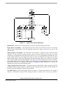
Power Factor Correction (PFC) Theory
The main idea of the PFC algorithm is the transformation of an input current waveform into be a sine signal
with the same input voltage frequency. IEC standards do not require ideal sine waveform for compatibility;
providing simple three-point approximation is sufficient. In this case, the current waveform will be nearly
rectangular; this simplification saves processor resources. The hardware control of the inverter power switch is
the second step of simplification. For this approach, the hardware provides instant value of the PFC input
current. Thus, software controls only the average value and does not have direct access to the inverter switch;
see Figure 3-1.
The system is designed to provide power supply with a maximum 180W power. The system incorporates the
following hardware circuits:
•
Power supply rectifier
•
Boost inverter
•
Hardware Pulse Width Modulator (PWM)
•
Zero-crossing detector
•
Output voltage sensor
•
56F80x or 56F83xx Evaluation Module (EVM)
Design of Indirect Power Factor Correction, Rev. 1
Freescale Semiconductor
3
Power Factor Correction (PFC) Theory
L
Load
T
~115V 60Hz
~230V 50Hz
= 385V
D
C
External Pulse Width Modulator
VREF
&
Zero
crossing
Zero-crossing
detection
Detection
Pulse Width
Modulation
Input Frequency
Measurement
Base
Frequency
Milestone
Generation
Inhibit
Output
Output Voltage
Measurement
Reference
Voltage
Calculation
56F800/E
Figure 3-1. System Concept
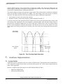
The Control Process
The PFC performs correction of the input current waveform. The standard power supply with a rectifier and
large electrolytic capacitor has an excessive peak of input current. This peak appears when the voltage from the
rectifier is greater than the voltage on the capacitor; see Figure 3-2.
Design of Indirect Power Factor Correction, Rev. 1
4
Freescale Semiconductor
Standard Power Supply:
Power Factor Corrector:
Output voltage
Output voltage
Input current
Input current
Figure 3-2. Waveforms of Output Voltage and Input Current
To produce the rectangular input current waveform, an active PFC is placed between the rectifier and the
filtering capacitor. This is a boost inverter consisting of an inductor (L), diode (D) and chop switcher (T). If the
switcher (T) is on at any phase position of AC input voltage, the diode is reversed-biased, thus isolating the
filtering capacitor. In this period, the input supplies energy to inductor (L). When switcher (T) is off, the
filtering capacitor is charged from the inductor as well as from the input, thus providing input current with
continuous conduction.
The Pulse Width Modulator (PWM) generates reference pulses with a frequency of about 20KHz. The duty
cycle of PWM pulses can be modified in two points:
1. The average duty cycle (a period longer than one period of input voltage) depends on output load. High
output load requires a longer transistor open state to support the constant output voltage.
2. The instant duty cycle (a period less than one-half of the period of input voltage) depends on input voltage.
Low input voltage requires a longer transistor open state to support the constant input current.
A rectangular waveform provides a narrow spectrum of noise and the lowest peak value of input current
because the high frequency task of inverter switching can be filtered easily.
Design of Indirect Power Factor Correction, Rev. 1
Freescale Semiconductor
5
System Design Concept
This hardware implementation does not allow direct modification of the pulse duty cycle that feeds to the
switcher (T). The reference voltage of the external PWM comes from a filtered PWM signal from the
controller, and can be set according to input voltage zero crossing, base frequency, and output voltage.
Therefore, the only analog feedback for device control is output voltage. This implementation is called indirect
PFC and can save the controller’s resources.
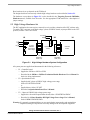
The best shape for the input current is a sinusoid shape. But to reduce complexity and meet standard
requirements, this PFC application utilizes the simplest 3-points approximation, illustrated in Figure 3-3. The
desired shape is the result of optimization, and fulfills the following requirements:
•
Less complexity and avoids overloading the controller (the majority of resources arereserved for motor
control)
•
Harmonic content which complies with the standard IEC 1000-3-2
1204µs
Input Current
382µs
Time
Input voltage waveform
Input current waveform
Figure 3-3. Input Current Waveform
4.
System Design Concept
The system was designed in accordance with the following performance specifications:
•
Targeted for 56F800/E EVM platforms
•
Input power supply voltage 230V 50Hz or 115V 60Hz
•
Output voltage is set up to 380V DC
•
Nominal output voltage is set to 385V DC
•
Nominal output power of up to 180W
•
Input current harmonic content will comply with standard IEC 1000-3-2
As shown in Figure 4-1, the PFC control algorithm performs the following tasks:
•
Converts sensed output voltage to a digital value
•
Software PID regulator for feedback loop
•
Programs the PWM channel, creating a pattern of the input current
•
Synchronizes operation to the power line frequency, using mean zero-crossing detector
Design of Indirect Power Factor Correction, Rev. 1
6
Freescale Semiconductor
Start
Initialize
Wait for mains
zero crossing
Set timer
Wait for output
compare
Select milestone
by pointer
Milestone 1
Milestone 2
Milestone 3
Milestone 4
Activate inhibit
Deactivate inhibit
Program PWM
Program PWM
Read Vout
Reset pointer
PID regulator
Program PWM
Increment pointer
Figure 4-1. Indirect PFC Control Flowchart
Initialization - Initializes the on-chip peripherals, power line voltage and frequency detection
Input capture event handler - After initialization, the PFC software waits for the power lines’ zero-crossing
signal, used for synchronization of the PFC algorithm with the line voltage, and sets the time_base for the
milestone table.
Output compare event handler - The main task of the function is to define the input current waveform
milestones, or time intervals, forming the input current waveform. During each step, the next output
comparison is programmed and the proper input current level is set by programming the PWM duty cycle.
Upon reaching a milestone of one of the input current waveform, the output DC bus voltage (Vout) is sensed
and the sensed voltage is fed into the PID regulator. The nominal output voltage is set to 385V DC. The output
of the voltage regulator represents the amplitude of the input current. The calculated input current is limited to
the maximum input value and zeroed if negative. New values representing the higher and lower level of the
input current waveform are calculated, and illustrated in Figure 3-3. When Milestone 4 is reached, the
algorithm waits for the next synchronization signal.
Analog-to-Digital Conversion routine - The routine reads the output DCBus voltage, required by the PFC
algorithm to sense the output voltage on a regular basis with a minimum period of 10ms. The ADC channel can
be shared with other applications running on the controller.
The PWM Signal is generated using Quad Timer D, Channel 1, in cascade with Channel 0. The output of
Channel 1 is connected to output pin TD1. Placing the timers in cascade mode is necessary to generate a
Design of Indirect Power Factor Correction, Rev. 1
Freescale Semiconductor
7
Hardware Implementation
sufficient PWM frequency, and recommended to be higher than 100kHz. After filtering the PWM signal, the
analog voltage is obtained. It corresponds with the required input current, fed to the analog comparator (the
external Pulse Width Modulator) switching the MOSFET.
The control technique is based on the hysteresis current control. The system operates in continuous conduction
mode with avariable switching frequency (30--80kHz). The desired shape of the input current is a staircase
waveform. The number and size of the stairs are optimized in order to fulfill these requirements:
•
•
Least complex to create a low load on the controller
Harmonic currents’ content which complies with the standard EN 61000-3-2
To provide current waveform generation, the PFC hardware has a subsystem which detects input voltage at the
zero crossing. This subsystem is the level comparator, generating pulses when the input voltage crosses a
particular level, illustrated in Figure 4-2. The center of the pulse is shifted from a real zero-crossing position
because of the comparator’s hysteresis characteristic. This shift can be recovered by the software, so a real
input voltage zero-crossing position can be resolved as the center of the zero-crossing pulse minus the offset
value.
Input Voltage
(after rectifier)
T
Zero-crossing
Signal Offset
Zero-crossing
Signal
T
Figure 4-2. Zero Crossing Signal Generation
5.
Hardware Implementation
5.1 System Outline
The hardware system is designed to drive the 3-phase AC/BLDC motor. The application note described here is
a PFC application example only and does not consider motor control. PFC can be easily integrated with any
motor control application.
Software is targeted for the following devices and Evaluation Module (EVMs):
•
56F805 and 56F805EVM
•
56F8346 and 56F8346EVM
Design of Indirect Power Factor Correction, Rev. 1
8
Freescale Semiconductor
High Voltage Hardware Set
How hardware is set up depends on the EVM used.
The designed software can run only with the high voltage hardware set described in Section 5.2.
The hardware set-up shown in Figure 5-1 is also described in the Targeting Freescale DSP5680x
Platform manual, available from Freescale. See the appropriate EVM manual for a description of
jumper settings.
5.2 High Voltage Hardware Set
The PFC application does not require a motor drive as it provides evaluation of the PFC software only.
To enable a PFC converter on the high voltage 3-phase AC/BLDC board, set jumper JP201 to the PFC
position; contacts 1 and 2 are closed.
+12V DC
GND
1
2
3
JP201
Optoisolation
Board
40W
Flat Ribbon
Cable, Gray
J1
3-phase
AC/BLDC
High Voltage
Power Stage
J1
PE
J14
J11.1
J11.2
J2
L
N
U1
U2
JP1.1
JP1.2
U3
Controller
Board
40W
Flat Ribbon
Cable, Gray
Figure 5-1. High Voltage Hardware System Configuration
All system parts are supplied and documented in the following references:
•
U1 - Controller board:
— Supplied as 56F80x or 56F83xx EVM
— Described in the 56F80x or 56F83xx Evaluation Module Hardware User’s Manual for
the device being implemented
•
U2 - Optoisolation board
— Supplied with 3-phase AC/BLDC high-voltage power stage;
Order # ECOPTHIVACBLDC
or
— Supplied alone, Order # ECOPT
— Described in Optoisolation Board User’s Manual
•
U3 - 3-phase AC/BLDC high-voltage power stage
— Supplied in a kit with an optoisolation board; Order # ECOPTHIVACBLDC
— Described in: 3-Phase Brushless DC High-Voltage Power Stage User’s Manual;
Order # MEMC3BLDCPSUM/D
Warning: It is strongly recommended that you use optoisolation (optocouplers and optoisolation
amplifiers) during development to avoid any damage to the development equipment.
Design of Indirect Power Factor Correction, Rev. 1
Freescale Semiconductor
9
Software Design
Note:
6.
A detailed description of individual boards can be found in the comprehensive user’s
manual for each board. The manual incorporates the schematic of the board, a
description of individual function blocks, and a bill of materials. Individual boards can be
ordered from Freescale as a standard product; see Section 9. for more information.
Software Design
This section describes the design of the drive’s software blocks. The software will be described in terms of:
•
Calculating reference voltage
•
Processing milestones
•
State diagram
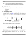
6.1 Calculating Reference Voltage
PFC software periodically updates reference voltage according to the present value of output voltage. The
reference value is calculated as the sum of its average value with the difference between measured output
voltage and its nominal value, shown in Figure 6-1. The structure contains the amplifier model, tasked with
performing the transformation u_dif = K * u_dif. It rescales the output voltage value, measured by the ADC
module, to the eight bits range of the PWM. The application uses the PWM output as a Digital-to-Analog
Converter.
u_out
u_dif
k
ref_voltage
K*u_dif
f()
PFC_OUTPUT_VOLTAGE
F(ref_voltage)
Figure 6-1. Reference Voltage Calculation
The reference voltage calculation algorithm uses the DCBus voltage value, measured by the ADC module in
the Motor Control portion of the software. The DCBus value has the following scale:
Table 6-1. DCBus Voltage Scale
DCBus Voltage
Frac16 u_out
Comments
0V
0.0
zero level
407V
1.0
full scale
The function f() is a filter algorithm like a simple Resistance-Capacitance (RC) circuit. The filter time constant
depends on the PFC hardware implementation and defines the output characteristic of the PFC output voltage.
The smaller time constant value provides a quicker output voltage response, but with less stable behavior.
Warning: Reference voltage calculation coefficients and algorithm depend directly on PFC hardware
implementation.
Design of Indirect Power Factor Correction, Rev. 1
10
Freescale Semiconductor
Milestone Generation
6.2 Milestone Generation
The reference voltage value is corrected during the period of input voltage to provide the input current
waveform illustrated in Figure 3-1. When the zero-crossing signal comes, the program calculates the
zero-crossing pulse length and synchronizes the processes of milestone generation with input
frequency; see Figure 6-2.
time_base
compare_value
rising-edge
arrival time
MILESTONE_OFFSET
pulse_length
f()
falling-edge
arrival time
Figure 6-2. Milestones Synchronization Algorithm
Zero-crossing Signal
Output Compare Match
Input Capture Event
Output Compare Interrupt
Reset Pointers
Update Output Compare Register
Milestone
Time Table
time_table_ptr
Increment Pointer
Execute Milestone Callback
Milestone
Callback Table
callback_table_ptr
Increment Pointer
Figure 6-3. Milestone Generation
The resolved value defines the first milestone point, a timer interrupt on the output compare event.
Each time the output compare matches the interrupt, the compare register accrues toward the next
milestone. Milestone generation time intervals are stored in the Milestone Time Table. They have
Design of Indirect Power Factor Correction, Rev. 1
Freescale Semiconductor
11
Software Design
constant values during the half-period of input voltage. The Output Compare Event service routine invokes
function from the Milestone Callback Table, which performs calculation and correction of PFC reference value
or activates inhibit output. This procedure allows easy modification of the sequence of events.
6.3 State Diagram
PFC control operates from event handlers and excludes peripheral initialization and DCBus voltage
measurement. The PFC control is developed to easily incorporate motor control applications. The Main routine
calls to the PFC initialization function and passes the value of the DCBus voltage to PFC control, allowing
measurement of DCBus voltage with different sample rates and ADC modes. This application demonstrates
initialization and use of PFC control.
6.3.1 Application State Machine
The Main routine provides:
•
•
•
•
•
•
Initialization of the Analog-to-Digital Converter
Initialization of the Timer
Initialization of the Switch and LEDs
Initialization of Brake control
Initialization of the PFC routine call
Application main loop
Application Start
Disable Interrupts
Initialization of the Application
Initialization of the PFC Routine Call
Enable Interrupts
Check Application State
No Faults
Fault Occurs
Check Switch State
Switch ON
Enable PFC Control
Fault Indication
Switch OFF
Disable PFC Control
Figure 6-4. Application State Machine
Design of Indirect Power Factor Correction, Rev. 1
12
Freescale Semiconductor
Bean Modules
7.
Software Implementation
This project is implemented using Processor Expert plug-in and Embedded Beans™ technology in the
CodeWarrior Integrated Devolopment Environment (IDE). Processor Expert is designed for rapid
application development of embedded applications on many platforms.
7.1 Embedded Beans
Embedded Beans are design components which encapsulate functionality of basic elements of
embedded systems, such as the controller’s core; on-chip peripherals; stand-alone peripherals; virtual
devices; and pure software algorithms. Embedded Beans allow access to these facilities via simple and
uniform interface of properties, methods, and events. Additional information can be found in Processor
Expert help.
Table 7-1 and Table 7-2 list the beans used to implement the application.
7.2 Bean Modules
Each peripheral on the controller chip or on the EVM board is accessible through a bean. Processor
Expert generates the source code modules containing the implementation of methods controlling the
hardware which provides the bean’s functionality.
The following steps are required to generate the code:
•
Add the beans to your project (Processor Expert tab of CodeWarrior’s project panel)
•
Set up the beans according to the hardware configuration
•
Generate the source code
•
Use beans methods in your code (generated functions for beans methods are named
beanName_MethodName)
You should not modify generated modules; generated code can be found in the Files folder of
CodeWarriors’s project panel.
User modules, which you can modify, are found in the User Modules folder, where other user modules
can also be added. The Events module (events.c) contains the handling routines for beans’ events, for
example, those caused by interrupt. The Main module (projectName.c) contains the function main()
and all necessary declarations and variables.
All enabled methods are generated into appropriate bean modules during the code generation process.
Every beans method inserted into the project is visible as a subtree of the bean in the Project panel
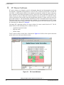
(found under the Processor Expert tab of CodeWarrior’s project panel). Figure 7-1 shows the beans
inserted in the project for a 56F805 implementation; a detailed description of beans is shown in
Table 7-1. See Figure 7-2 for an illustration of beans used in a 56F8346 implementation and
Table 7-2 for a detailed description of beans used in that implementation.
Design of Indirect Power Factor Correction, Rev. 1
Freescale Semiconductor
13
Software Implementation
Figure 7-1. Beans Used in Implementing the 56F805
Table 7-1. Beans Used in Implementing the 56F805
Bean name
Bean type
Description
PC_M1
PC_Master
Provides serial communication with PC_Master software
running on a PC using the SCI0 on-chip device.
Communication speed is 9600bps.
adcPrimary
PI_ADC
Measures the output voltage
tmrD2
PI_TMR
Zero-crossing input
tiAux
TimerInt
Auxilary timer 20ms base
Design of Indirect Power Factor Correction, Rev. 1
14
Freescale Semiconductor
Bean Modules
Figure 7-2. Beans Used in Implementing the 56F8346
Table 7-2. Beans Used in Implementing the 56F8346
Bean name
Bean type
Description
PC_M1
PC_Master
Provides serial communication with the PC_Master software
running on PC using SCI0 on-chip device. Speed of communication is 9600 bps.
adcPrimary
PI_ADC
Measures the output voltage.
tmrD1
PI_TMR
Zero crossing input.
tiAux
TimerInt
Auxilary timer 20 ms base.
Design of Indirect Power Factor Correction, Rev. 1
Freescale Semiconductor
15
Software Implementation
7.3 PFC Control Integration
7.3.1 Resources
PFC control uses some of the controller’s peripherals and cannot share resources with the motor
control application (excluding the ADC channel for DCBus voltage measurement). The following
resources are allocated to PFC control:
•
Quad Timer module D, Channel 0
•
Quad Timer module D, Channel 1
•
Quad Timer module D, Channel 2
•
Quad Timer module C, Channel 0 (56F805 only)
7.3.2 Modification
Place the following line in the main program to provide access to the PFC control API functions:
#include “PE_dpfc.h”
7.4 PFC Control Constants
This section describes constants, located in the main module. It defines the waveform of the PFC input
current.
MILESTONE_OFFSET defines the time between the rising edge of the zero-crossing signal and the
first milestone point. This time depends on the zero-crossing detection subsystem of the PFC
hardware, which can be measured. The MKS_TO_TICK() macro allows the definition value to be
expressed in microseconds.
Example:
#define MILESTONE_OFFSET MKS_TO_TICK(820L)
MilestoneTime is the array of the milestones’ time intervals. Its values depend on the current waveform
to be generated. The MKS_TO_TICK() macro allows the definition value to be expressed in
microseconds.
Example:
const UWord16 MilestoneTime[] ={
MKS_TO_TICK(411L),
MKS_TO_TICK(382L),
MKS_TO_TICK(411L),
MKS_TO_TICK(5500L),
MKS_TO_TICK(5000L),
NULL,/* End of time table */ };
MilestoneCallback is the array of pointers to the functions to be executed. These functions occur after
each corresponding time interval is defined in MilestoneTime[], control PFC reference voltage and
inhibit output.
Design of Indirect Power Factor Correction, Rev. 1
16
Freescale Semiconductor
PFC Control API
Example:
/* Forward function declaration */
void PFC_SetLowGain(void);
void PFC_SetHighGain(void);
void PFC_ForceInhibit(void);
const pfc_tCallback* MilestoneCallback[] = {
PFC_SetLowGain,
PFC_ForceInhibit,
PFC_SetLowGain,
PFC_SetHighGain,
PFC_EnableZCDetection,
NULL,
/* End of callback table */
7.5 PFC Control API
This section describes the main PFC control functions, permitting PFC features to be used in the main code.
7.5.1 PFC_Init
Prototype:
void PFC_Init(void);
This function initializes the PFC on-chip peripherals.
7.5.2 PFC_SetUOut
Prototype:
void PFC_SetUOut(UInt16 u_dc_bus);
This function allows the DCBus voltage value to pass to PFC control. The refresh rate of this value must be no
less than the input voltage frequency.
7.5.3 PFC_Enable
Prototype:
void PFC_Enable(void);
This function enables PFC control to start the conversion after the first zero-crossing pulse.
Notes:
Do not enable PFC control until measurement of DCBus voltage is complete.
7.5.4 PFC_Disable
Prototype:
void PFC_Disable(void);
This function disables PFC control to immediately finish the PFC conversion.
Notes:
After finishing the PFC conversion, output voltage has no zero level. Its value depends on input
voltage and equals about 1.4*UIN.
Design of Indirect Power Factor Correction, Rev. 1
Freescale Semiconductor
17
PC Master Software
8.
PC Master Software
PC master software was designed to provide a debugging, diagnostic and demonstration tool for the
development of algorithms and applications. It runs on a PC connected to the EVM via an RS-232
serial cable. A small program resident in the controller communicates with the PC master software to
parse commands, return status information to the PC, and process control information from the PC. PC
master software uses part of Microsoft's Internet Explorer as the user interface. To enable PC master
software operation on the controller target board application, add the PC master software bean to the
project and configure it. This automatically includes the SCI driver and installs all necessary services.
The default baud rate of the SCI communication is 9600bd. It is set automatically by the PC master
software driver and can be changed if needed. A detailed description of PC master software is provided
in a dedicated User's Manual; see Section 9.
The digital PFC application utilizes PC master software for remote control from the PC. The PC
master software reads and displays these variables to the user:
•
Application operational mode
•
Start/stop status
•
DCBus voltage
The PC master software Control Page is illustrated in Figure 8-1. Profiles of the required and actual
speeds can be seen in the Speed Scope window.
Figure 8-1. PC Control Window
Design of Indirect Power Factor Correction, Rev. 1
18
Freescale Semiconductor
PFC Control API
9.
References
1. DSP56800 16-Bit Digital Signal Processor Family Manual, DSP56F800FM, Freescale Semiconductor
2. DSP56800E 16-Bit Digital Signal Processor Reference Manual, DSP56800ERM, Freescale
Semiconductor
3. 56F805 Evaluation Module Hardware User’s Manual, DSP56F805EVMUM, Freescale Semiconductor
4. 56F8346 Evaluation Module Hardware User’s Manual, MC56F8346EVMUM, Freescale Semiconductor
5. DSP56F80x 16-Bit Digital Signal Processor User’s Manual, DSP56F801-7UM, Freescale Semiconductor
6. Optoisolation Board User’s Manual, MEMCOBUM, Freescale Semiconductor
7. 3-Phase Brushless DC High Voltage Power Stage, MEMC3PBLDCPSUM, Freescale Semiconductor
8. Processor Expert Embedded Beans, Processor Expert Help
For additional information:
www.freescale.com
Design of Indirect Power Factor Correction, Rev. 1
Freescale Semiconductor
19
How to Reach Us:
Home Page:
www.freescale.com
E-mail:
[email protected]
USA/Europe or Locations Not Listed:
Freescale Semiconductor
Technical Information Center, CH370
1300 N. Alma School Road
Chandler, Arizona 85224
+1-800-521-6274 or +1-480-768-2130
[email protected]
Europe, Middle East, and Africa:
Freescale Halbleiter Deutschland GmbH
Technical Information Center
Schatzbogen 7
81829 Muenchen, Germany
+44 1296 380 456 (English)
+46 8 52200080 (English)
+49 89 92103 559 (German)
+33 1 69 35 48 48 (French)
[email protected]
Japan:
Freescale Semiconductor Japan Ltd.
Headquarters
ARCO Tower 15F
1-8-1, Shimo-Meguro, Meguro-ku,
Tokyo 153-0064, Japan
0120 191014 or +81 3 5437 9125
[email protected]
Asia/Pacific:
Freescale Semiconductor Hong Kong Ltd.
Technical Information Center
2 Dai King Street
Tai Po Industrial Estate
Tai Po, N.T., Hong Kong
+800 2666 8080
[email protected]
For Literature Requests Only:
Freescale Semiconductor Literature Distribution Center
P.O. Box 5405
Denver, Colorado 80217
1-800-441-2447 or 303-675-2140
Fax: 303-675-2150
[email protected]
Information in this document is provided solely to enable system and
software implementers to use Freescale Semiconductor products. There are
no express or implied copyright licenses granted hereunder to design or
fabricate any integrated circuits or integrated circuits based on the
information in this document.
Freescale Semiconductor reserves the right to make changes without further
notice to any products herein. Freescale Semiconductor makes no warranty,
representation or guarantee regarding the suitability of its products for any
particular purpose, nor does Freescale Semiconductor assume any liability
arising out of the application or use of any product or circuit, and specifically
disclaims any and all liability, including without limitation consequential or
incidental damages. “Typical” parameters that may be provided in Freescale
Semiconductor data sheets and/or specifications can and do vary in different
applications and actual performance may vary over time. All operating
parameters, including “Typicals”, must be validated for each customer
application by customer’s technical experts. Freescale Semiconductor does
not convey any license under its patent rights nor the rights of others.
Freescale Semiconductor products are not designed, intended, or authorized
for use as components in systems intended for surgical implant into the body,
or other applications intended to support or sustain life, or for any other
application in which the failure of the Freescale Semiconductor product could
create a situation where personal injury or death may occur. Should Buyer
purchase or use Freescale Semiconductor products for any such unintended
or unauthorized application, Buyer shall indemnify and hold Freescale
Semiconductor and its officers, employees, subsidiaries, affiliates, and
distributors harmless against all claims, costs, damages, and expenses, and
reasonable attorney fees arising out of, directly or indirectly, any claim of
personal injury or death associated with such unintended or unauthorized
use, even if such claim alleges that Freescale Semiconductor was negligent
regarding the design or manufacture of the part.
Freescale™ and the Freescale logo are trademarks of Freescale Semiconductor,
Inc. All other product or service names are the property of their respective owners.
This product incorporates SuperFlash® technology licensed from SST.
© Freescale Semiconductor, Inc. 2005. All rights reserved.
AN1965
Rev. 0
07/2005