1
Semiconductor Application Note
Order by AN1919/D
(Motorola Order Number)
Rev. 1.0, 4/01
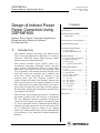
Contents
Design of Indirect Power
Factor Correction Using
DSP56F80X
1. Introduction ................................... 1
Indirect Power Factor Correction Application
Design based on Motorola Software
Development Kit
3. Power Factor Correction Theory... 3
1.
Introduction
This document describes the design of an Indirect Power
Factor Correction (Indirect PFC) application. It is based on
Motorola’s 56F803/805 Digital Signal Processor (DSP),
dedicated to motor control applications.
Most practical electronic power supplies consist of a
conventional, single-phase, full-bridge rectifier, and filter
stages. Already well-established, this type of circuit draws
high current levels from the power line, producing a high
level of harmonics. This harmonic distortion and low power
factor (PF) reduces the maximum power available from
power lines, thereby decreasing the efficiency of the
electrical power grid. The European Normative EN
61000-3-2 defines the limits of the harmonic content of the
input current for the power line supplied equipment. To meet
these requirements, new designs require the use of an active
power factor correction (PFC) at the input. The PFC emulates
the ideal ohmic load through electronically controlled input
current drawn from the line.
There are many specific integrated circuits (IC) available on
the market to perform a PFC task. However, to perform the
PFC task, additional electronic components increasing the
system cost and complexity are required. Alternatively, there
is a way to implement the PFC control through the DSP in
addition to the main control tasks such as motor control. The
use of a digital PFC replaces a number of ICs, reducing
system cost. Another benefit of the software implementation
is the possibility of easy modification without changing the
hardware.
© Motorola, Inc., 2001
2. Motorola DSP Advantage
and Features ............................. 2
4. System Design Concept ................ 5
5. Hardware Implementation............. 8
5.1 System Outline ............................... 8
5.2 High Voltage Hardware Set............ 8
6. Software Design ............................ 9
6.1 Reference Voltage Calculation ....... 9
6.2 Milestone Generation.................... 10
6.3 State Diagram ............................... 11
6.3.1 Application State Machine ....... 11
7. SDK Implementation .................. 12
7.1 Files .............................................. 12
7.2 Drivers and Library Function ....... 13
7.3 Appconfig.h file............................ 13
7.4 PFC Control Constants ................. 14
7.5 PFC Control API .......................... 15
7.5.1 PFC_Init ................................... 15
7.5.2 PFC_SetUOut........................... 15
7.5.3 PFC_Enable.............................. 15
7.5.4 PFC_Disable ............................ 15
7.5.5 PC Master................................. 15
8. Memory Usage ............................ 16
9. References ................................... 16
Indirect Power Factor Correction
MOTOROLA
Motorola DSP Advantage and Features
The indirect PFC design featured here satisfies the minimum DSP performance requirements. The
design is suitable for applications where the load of the DSP is high and the available resources are
low.
This application note presents the concept of the continuous conduction current mode boost power
factor corrector (PFC) with nominal output power of 180W. The PFC is digitally controlled by a
digital signal processor (DSP).
2.
Motorola DSP Advantage and Features
The Motorola DSP56F80x family is well suited for digital motor control, combining the calculation
capability of DSPs with MCUs controller features on a single chip. These DSPs offer a rich, dedicated
peripherals set like pulse-width-modulation (PWM) unit, analog-to-digital converter (ADC), Timers,
communication peripherals (SCI, SPI, CAN), on-board Flash, and RAM. Each family chip is well
suited for reliable motor control tasks.
A typical family member, the DSP56F805, provides the following peripheral blocks:
•
Two Pulse Width Modulator modules each with six PWM outputs, three Current Sense inputs, and
four Fault inputs, fault tolerant design with dead-time insertion; supports both center- and
edge-aligned modes
•
Two 12-bit Analog-to-Digital Converters (ADC) which support two simultaneous conversions;
ADC and PWM modules can be synchronized
•
Two Quadrature Decoders each with four inputs or two additional Quad Timers
•
Two General Purpose Quad Timers totaling six pins: Timer C with two pins and Timer D with four
pins
•
CAN 2.0 B Module with 2-pin port for transmit and receive
•
Two Serial Communication Interfaces, each with two pins (or four additional GPIO lines)
•
Serial Peripheral Interface (SPI) with configurable four-pin port (or four additional GPIO lines)
•
14 dedicated General Purpose I/O (GPIO) pins, 18 multiplexed GPIO pins
•
Computer Operating Properly (COP) watchdog timer
•
Two dedicated external interrupt pins
•
External reset input pin for hardware reset
•
External reset output pin for system reset
•
JTAG/On-Chip Emulation (OnCE™) module for unobtrusive, processor speed-independent
debugging
•
Software-programmable, Phase Lock Loop-based frequency synthesizer for the DSP core clock
•
Memory configuration
— 32252 × 16-bit words of program flash
— 512 × 16-bit words of program RAM
— 2K × 16-bit words of data RAM
— 4K × 16-bit words of data flash
— 2K × 16-bit words of boot flash
2
Indirect Power Factor Correction
Power Factor Correction Theory
3.
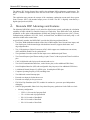
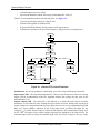
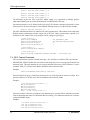
Power Factor Correction Theory
The main idea of the power factor correction algorithm is the input current waveform transformation to
be a sine signal having the same input voltage frequency. IEC standards do not require ideal sine
waveform for compatibility. It is enough to provide simple three-point approximation. In this case the
current waveform will be nearly rectangular. This simplification saves processor resources. The
hardware control of the inverter power switch is the next step of simplification. For this approach the
hardware provides instant value of the PFC input current. Thus, software controls the average value
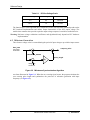
only and does not have direct access to the inverter switch. See Figure 3-1.
L
T
~115-230V
50/60Hz
= 360V
D
load
C
external pulse width modulator
Vref
&
Zero
Zero crossing
crossing
detection
detection
Input
frequency
measurement.
Milestone
generation.
Pulse width
modulation
Inhibit
output
Base
frequency
Output voltage
measurement
Reference
voltage
calculation
DSP56F80X
Figure 3-1 System Concept
The system is designed to provide power supply with maximum 180W power. The system
incorporates the following hardware circuits:
Indirect Power Factor Correction
3
Power Factor Correction Theory
•
Power supply rectifier
•
Boost inverter
•
Hardware pulse wide modulator
•
Zero crossing detector
•
Output voltage sensor
•
Evaluation board DSP56F803 or DSP56F805
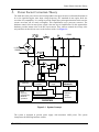
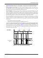
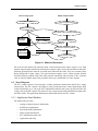
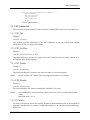
The Control Process
The power factor corrector (PFC) performs correction of the input current waveform. The standard
power supply with rectifier and large electrolytic capacitor has excessive peak of input current. This
peak appears when voltage from rectifier is greater than voltage on the capacitor (see Figure 3-2).
Standard Power Supply:
Power Factor Corrector:
Output voltage
Output voltage
Input current
Input current
Figure 3-2 Waveforms of Output Voltage and Input Current
To produce the rectangular input current waveform, an active power factor corrector is placed between
the rectifier and the filtering capacitor. This is a boost inverter consisting of an inductor (L), diode (D)
and chop switcher (T). If switcher (T) is on at any phase position of AC input voltage, the diode is
reversed biased, thus isolating the filtering capacitor. In this period, the input supplies energy to
inductor (L). When switcher (T) is off, the filtering capacitor is charged from the inductor as well as
from the input. Thus providing input current with continuous conduction.
4
Indirect Power Factor Correction
System Design Concept
Pulse width modulator generates reference pulses with a frequency of about 20KHz. The duty cycle of
PWM pulses can be modified in two points:
1. Average duty cycle (time longer than one period of input voltage) depends on output load. High
output load requires longer time of transistor open state to support the constant output voltage.
2. Instant duty cycle (time less than one half of period of input voltage) depends on input voltage.
Low input voltage requires longer time of transistor open state to support constant input current.
Rectangular waveform provides a narrow spectrum of noise and lowest peak value of input current
because the high frequency part of inverter switching can be filtered easily.
This hardware implementation does not allow direct modification of the pulse duty cycle that feeds to
switcher (T). Reference voltage of external pulse width modulator comes from a filtered DSP PWM
signal. This DSP PWM signal can be set according to input voltage zero crossing, base frequency, and
output voltage. Therefore the only analog feedback for DSP control is output voltage. This
implementation is called indirect PFC and can save DSP resources.
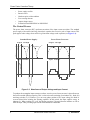
The best shape of the input current is the sinusoid. But for reducing complexity and meet standard
requirements, this PFC application utilizes simplest 3-points approximation, illustrated in Figure 3-3.
The desired shape is the result of optimization, and fulfills the following requirements:
•
Less complexity, avoiding overloading of the DSP (most part of resources is reserved for
motor control)
•
Harmonic content complies with standard IEC 1000-3-2
1204µs
Input Current
382µs
Time
Input voltage waveform
Input current waveform
Figure 3-3 Input Current Waveform
4.
System Design Concept
The system was designed in accordance with the following performance specifications:
•
Targeted for DSP56F803/805EVM platforms
•
Input power supply voltage 115-230V AC
•
Input power supply frequency 50/60Hz
•
Nominal output voltage up to 360V DC
Indirect Power Factor Correction
5
System Design Concept
•
Nominal output power up to 180W
•
Input current harmonic content will comply with standard IEC 1000-3-2
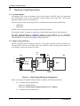
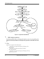
The PFC control algorithm performs the following tasks. See Figure 4-1.
•
Converts sensed output voltage to a digital value
•
Software PID regulator for feedback loop
•
Programs the PWM channel, creating a pattern of the input current
•
Synchronizes operation to the power line frequency, using mean zero crossing detector
Start
Initialise
Wait for mains
zero crossing
Set timer
Wait for output
compare
Select milestone
by pointer
1.milestone
2.milestone
3.milestone
4.milestone
Activate inhibit
Deactivate inhibit
Program PWM
Program PWM
Read Vout
Reset pointer
PID regulator
Program PWM
Increment pointer
Figure 4-1 Indirect PFC Control Flowchart
Initialization - the on-chip peripherals’ initialization, power line voltage and frequency detection.
Input capture ISR - After the initialization the PFC software waits for the power lines zero crossing
signal, used for synchronization of the PFC algorithm with the line voltage, the time_base for the
milestone table is set.
Output compare ISR - The main task of the function is to define the input current waveform
milestones, or time intervals, hence forming the input current waveform. During each step the next
output comparison is programmed and the proper input current level is set by programming the PWM
duty cycle. Upon reaching a milestone of one of the input current waveform, the output DC bus
voltage (Vout) is sensed. Sensed voltage is fed into the PID regulator. The nominal output voltage is set
to 385 VDC. The output of the voltage regulator represents the amplitude of the input current. The
calculated input current is limited to maximum input value and zeroed if negative. The new values
6
Indirect Power Factor Correction
System Design Concept
representing the higher and lower level of the input current waveform are calculated, and illustrated in
Figure 3-3. Reaching milestone four, the algorithm is waiting for the next synchronization signal.
Analog-to-Digital Conversion ISR - The routine reads the output dc-bus voltage. It is required by the
PFC algorithm to sense the output voltage regularly with a minimum period of 10ms. The ADC
channel can be shared with other applications running on the DSP.
The PWM Signal is generated using quad timer D, channel one, in cascade with channel zero. The
output of channel one is connected to the output pin TD1. Placing the timers in cascade mode is
necessary to generate a sufficient PWM frequency, and recommended to be higher than 100kHz. After
filtering the PWM signal, the analog voltage is obtained. It corresponds with the required input current,
fed to the analog comparator (external Pulse Width Modulator) switching the MOSFET.
The control technique is based on the hysteresis current control. The system operates in continuous
conduction mode with variable switching frequency (30 - 80kHz). The desired shape of the input
current is a staircase waveform. The number and size of the stairs are optimized in order to fulfill these
requirements:
•
•
Least complex to get low load of the DSP
Harmonic currents content complying with standard EN 61000-3-2
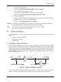
To provide a current waveform generation, the PFC hardware has a subsystem detecting input voltage
at the zero crossing. This subsystem is the level comparator generating pulses when the input voltage
crosses a particular level. This is illustrated in Figure 4-2. The center of pulse is shifted from a real
zero crossing position because of the comparator hysteresis characteristic. This shift can be recovered
by the software. So, a real input voltage zero crossing position can be resolved as the center of zero
crossing pulse minus offset value.
Input voltage
(after rectifier)
T
Zero crossing
signal offset
Zero crossing
signal
T
Figure 4-2 Zero Crossing Signal Generation
Indirect Power Factor Correction
7
Hardware Implementation
5.
Hardware Implementation
5.1 System Outline
The hardware (HW) system is designed to drive the three-phase AC/BLDC motor. The application
note described here is only a PFC application example without motor control. PFC can be easily
integrated with any motor control application.
There are software (SW) versions targeted for a real DSP and evaluation module (DSP/EVM):
•
DSP56F803
•
DSP56F805
The HW setup only depends on the evaluation module (EVM) applied.
The designed software is capable of running only with the high voltage HW set described below.
The HW setup described in Figure 5-1 below is also described in the documents
Targetting_DSP56803_Platform, Targetting_DSP56805_Platform, both available from Motorola.
These documents also contain EVM jumper setting descriptions.
5.2 High Voltage HW Set
The PFC application does not require the motor drive. It provides evaluation of the PFC software only.
To enable a PFC converter on the high voltage 3ph AC/BLDC board, the jumper JP201 shall be in
PFC position. Contacts one and two are closed.
+12VDC
GND
U3
J1
J2
Optoisolation
Board
Controller
Board
JP201
1
2
3
3ph AC/BLDC
High Voltage
Power Stage
J1
PE
JP1.1
JP1.2
J11.1
J11.2
J14
L
N
U1
U2
40w flat ribbon
cable, gray
40w flat ribbon
cable, gray
Figure 5-1 High Voltage HW System Configuration
All the system parts are supplied and documented according to the following references:
•
U1 - Controller board for DSP56F805:
— supplied as: DSP56805EVM
— described in: DSP Evaluation Module Hardware User’s Manual
•
8
U1 - Controller board for DSP56F803:
Indirect Power Factor Correction
Software Design
— supplied as: DSP56803EVM
— described in: DSP Evaluation Module Hardware User’s Manual
•
U2 - 3 ph AC/BLDC high voltage power stage
— supplied in kit with optoisolation board as: ECOPTHIVACBLDC
— described in: Three Phase Brushless DC High Voltage Power Stage
•
U3 - Optoisolation board
— supplied with three phase AC/BLDC high voltage power stage as: ECOPTHIVACBLDC
— or supplied alone as: ECOPT - optoisolation board
— described in: Optoisolation Board User’s Manual
Warning: It is strongly recommended to use optoisolation (optocouplers and optoisolation amplifiers)
during development to avoid damage to the development equipment.
Note:
6.
Information of all mention boards and documents above can be located at:
http://mot-sps.com/motor/devtools/index.html.
Software Design
This section describes the design of the software blocks of the drive. The software will be described in
terms of:
•
Reference voltage calculation
•
Milestones processing
•
State diagram
6.1 Reference Voltage Calculation
PFC software periodically updates reference voltage according to the present value of output voltage.
Reference value is calculated as the sum of its average value with difference between measured output
voltage and its nominal value, shown in Figure 6-1. The structure contains the amplifier model, tasked
with performing transformation u_dif = K * u_dif. It rescales the output voltage value, measured by
the ADC module, to the eight bits range of the PWM. The application uses the PWM output as
digital-to-analog convertor.
u_out
u_dif
k
ref_voltage
K*u_dif
f()
PFC_OUTPUT_VOLTAGE
F(ref_voltage)
Figure 6-1 Reference Voltage Calculation
The reference voltage calculation algorithm uses the DC bus voltage value, measured by the ADC
module in the Motor Control portion of the software. The DC bus value has the following scale:
Indirect Power Factor Correction
9
Software Design
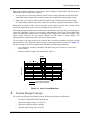
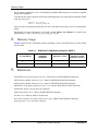
Table 6-1. DC-Bus Voltage Scale
DC-Bus Voltage
Frac16 u_out
Comments
0V
0.0
zero level
407 V
1.0
full scale
The function f() is a filter algorithm like a simple RC-circuit. The filter time constant depends on the
PFC hardware implementation and defines output characteristic of the PFC output voltage. The
smaller time constant value provides a quicker output voltage response, but with less stable behavior.
Warning: Reference voltage calculation coefficients and algorithm directly depend on PFC hardware
implementation.
6.2 Milestone Generation
The reference voltage value is corrected during the period of input voltage to provide the input current
time_base
compare_value
rising edge
arrival time
MILESTONE_OFFSET
pulse_length
f()
falling edge
arrival time
Figure 6-2 Milestones Synchronization Algorithm
waveform illustrated in Figure 3-1. When the zero crossing signal comes, the program calculates the
zero crossing pulse length and synchronizes the processes of milestone generation with input
frequency (see Figure 6-2).
10
Indirect Power Factor Correction
Software Design
Zero crossing signal
Output Compare match
Input Capture interrupt
Output compare interrupt
Reset pointers
Update output compare register
time_table_ptr
Milestone
time table
Increment pointer
Execute milestone callback
callback_table_ptr
Milestone
callback table
Increment pointer
Figure 6-3 Milestone Generation
The resolved value defines first milestone point, a timer interrupt on the output compare event. Each
time the output compare matches the interrupt, the compare register accrues toward the next milestone.
Milestone generation time intervals are stored in the milestone time table. They have constant values
during half-period of input voltage. The output interrupt compare service routine invokes function
from the milestone callback table. This table performs calculation and correction of PFC reference
value or activates inhibit output. This procedure allows easy modification of events sequence.
6.3 State Diagram
The PFC control operates from interrupts, excludes peripheral initialization and DC-bus voltage
measurement. The PFC control is developed to easily incorporate motor control applications. Main
routine functionality is to call to the PFC initialization function and to pass the measured DC-bus
voltage value to the PFC control. This allows DC-bus voltage measurement with different sample rates
and ADC modes. This application demonstrates initialization and use the PFC control.
6.3.1 Application State Machine
The Main routine provides:
•
Analog-to-digital converter initialization
•
POSIX timer initialization
•
Switch and LEDs initialization
•
Brake control initialization
•
PFC initialization routine call
•
Application main loop
Indirect Power Factor Correction
11
SDK Implementation
Application Start
Disable Interrupts
Application initialization
PFC Initialization Routine Call
Enable Interrupts
Check Application State
No Faults
Fault Occurs
Check Switch State
Switch ON
Enable PFC Control
Fault Indication
Switch OFF
Disable PFC Control
Figure 6-4 Application State Machine
7.
SDK Implementation
The Motorola embedded SDK is a collection of APIs, libraries, services, rules, and guidelines. This
software infrastructure is designed to let DSP5680x software developers create high-level, efficient,
portable code. This chapter describes how the Digital PFC application is written under SDK version
2.2.
7.1 Files
Application is composed of the following files:
12
•
...\dsp5680Xevm\nos\applications\Digital_PFC\Digital_PFC.c
(main program)
•
...\dsp5680Xevm\nos\applications\Digital_PFC\dpfc.c
(PFC control program)
•
...\dsp5680Xevm\nos\applications\Digital_PFC\Digital_PFC.mcp
(application project file)
Indirect Power Factor Correction
SDK Implementation
•
...\dsp5680Xevm\nos\applications\Digital_PFC\configflash\appconfig.c
(application configuration source file for FLASH)
•
...\dsp5680Xevm\nos\applications\Digital_PFC\configflash\appconfig.h
(application configuration header file for FLASH)
•
...\dsp5680Xevm\nos\applications\Digital_PFC\configflash\linker.cmd
(linker command file for FLASH)
•
...\dsp5680Xevm\nos\applications\Digital_PFC\configflash\flash.cfg
(configuration file for FLASH)
•
...\dsp5680Xevm\nos\applications\Digital_PFC\configextram\appconfig.c
(application configuration source file for external RAM)
•
...\dsp5680Xevm\nos\applications\Digital_PFC\configextram\appconfig.h
(application configuration header file for external RAM)
•
...\dsp5680Xevm\nos\applications\Digital_PFC\configextram\linker.cmd
(linker command file for external RAM)
Where X means type of target DSP (dsp56803evm or dsp56805evm)
These files are located in the SDK installation directory.
7.2 Drivers and Library Function
The three-phase AC induction V/Hz close loop motor control application uses the following drivers:
•
ADC driver
•
Quadrature timer driver
•
GPIO driver
•
Timer driver
•
LED driver
•
Switch driver
•
Brake driver
All drivers except the timer driver are included in the bsp.lib library. The timer driver is included in
sys.lib library.
Just ADC, MPIO and quadrature timer is necessary to provide PFC functionality. All other peripherals
are maintained for example only.
Each peripheral on the DSP chip or on the EVM board is accessible through driver. For detailed
description of drivers, see Embedded SDK (Software Development Kit) Targeting Motorola
DSP5680X Platform.
7.3 Appconfig.h file
The purpose of the appconfig.h file is to provide a mechanism for over-writing default static
configuration settings, defined in the config.h file. There are two appconfig.h files.
1. The first is dedicated to external RAM (..\ConfigExtRam directory).
2. The second is dedicated for FLASH memory (..\ConfigFlash directory).
In the case of digital PFC application, both files are nearly identical. The following lines are included
in the appconfig.h file to use PFC functionally:
Indirect Power Factor Correction
13
SDK Implementation
#define
#define
#define
#define
INCLUDE_USER_TIMER_D_0
INCLUDE_USER_TIMER_D_1
INCLUDE_USER_TIMER_D_2
INCLUDE_USER_TIMER_C_0
0
0
0
0
The difference in the two files is the PFC inhibit output. It is connected to multiple purpose
input/output (MPIO) pins or to timer dedicated pins for DSP56F805 EVM only.
One interrupt priority level is defined in the appconfig.h file. Because milestone generation is a time
critical process, one timer interrupt is to have highest interrupt priority; level three for this example:
#define GPR_INT_PRIORITY_32
3
The ADC initialization and service function sets ADC operating more. This module can be used in the
different modes. Application provides sample rate of DC-bus voltage measurement, required to be
sufficient for PFC control. Here is an example of ADC settings in appconfig.h:
/* ADC setting */
#define ADC_SCANMODE
#define ADC_INITIATE_SCAN
#define ADC_SET_DIVISOR
#define GPR_INT_PRIORITY_55
ADC_SEQUENTIAL_ONCE
ADC_INITIATE_SCAN_ON_START
6
2
/* ADC samples */
#define INCLUDE_ADCA_SAMPLE_0
/* ADC callbacks */
#define ADC_RAW_CONVERSION_COMPLETE_CALLBACK
CallbackADC_ISR
7.4 PFC Control Constants
This section describes constants, located in the dpfc.c file. It defines waveform of PFC input current.
MILESTONE_OFFSET defines the time between the rising edge of zero crossing signal and the first
milestone point. This time depends on zero crossing detection subsystem of PFC hardware. It can be
measured. MKS_TO_TICK() macro allows definition value in microseconds.
Example:
#define MILESTONE_OFFSET MKS_TO_TICK(820L)
Milestone50Hz is the array of milestones time intervals. Its values depend on current waveform, to be
generated. MKS_TO_TICK() macro allows definition value in microseconds.
Example:
const UWord16 Milestone50Hz[] = {
MKS_TO_TICK(411L),
MKS_TO_TICK(382L),
MKS_TO_TICK(411L),
MKS_TO_TICK(10000L),
NULL, /* End of time table */ };
MilestoneCallback is the array of pointers to the functions to be executed. Those functions occur after
each corresponding time interval is defined in Milestone50Hz[]. This functions controls PFC reference
voltage and inhibit output.
Example:
/* Forward function declaration */
void PFC_SetLowGain(void);
void PFC_SetHighGain(void);
void PFC_ForceInhibit(void);
14
Indirect Power Factor Correction
SDK Implementation
const pfc_tCallback* MilestoneCallback[] = {
PFC_SetLowGain,
PFC_ForceInhibit,
PFC_SetLowGain,
PFC_SetHighGain,
NULL,
/* End of callback table */ };
7.5 PFC Control API
This section describes the main PFC control functions, permitting PFC features use in the main code.
7.5.1 PFC_Init
Prototype:
void PFC_Init(void);
This function performs initialization of the DSP peripherals. It does not include ADC channel
initialization for DC bus voltage measurement.
7.5.2 PFC_SetUOut
Prototype:
void PFC_SetUOut(UInt16 u_dc_bus);
This function allows to pass DC bus voltage value to PFC control. Refresh rate of this value has to be
not less than input voltage frequency.
7.5.3 PFC_Enable
Prototype:
void PFC_Enable(void);
This function enables PFC control to start conversion after first zero crossing pulse.
Notes:
Beware to enable PFC control if DC-bus voltage measurement is not complete.
7.5.4 PFC_Disable
Prototype:
void PFC_Disable(void);
This function disables PFC control to immediately finish PFC conversion.
Notes:
After finishing PFC conversion output voltage has no zero level. Its value depends on input
voltage
and equals about 1.4*UIN
7.5.5 PC Master
PC master is designed to provide the profiling, diagnostic and demonstration tool for development of
algorithms and application. It consists of components running on a PC and parts running on the target
DSP device.
Indirect Power Factor Correction
15
Memory Usage
The PC master application is part of the Motorola embedded SDK and may be selectively installed
during SDK installation.
To enable the PC master operation on the target board application, the following lines should be added
to the appconfig.h file:
#define SCI_DRIVER
#define INCLUDE_PCMASTER
These two lines automatically include the SCI driver and install all necessary services for running PC
master.
The detailed PC master description is provided by the PC Master User Manual. It is stored at the
SDK directory as \sdk\pc_master\dsp_gui_um\dsp_gui_um.pdf.
8.
Memory Usage
Table 8-1 shows the PFC application memory consuming. A part of the DSP memory is still available
for other tasks.
Table 8-1.
9.
RAM and FLASH Memory Usage for SDK2.2
Memory
(In 16 Bit Words)
Available
DSP56F803
DSP56F805
Used
Application + Stack
Used
Application without
PC Master, SCI, Ident.
Program FLASH
32K
8572
4395
Data RAM
2K
564+352
196+352
References
DSP56F800 16-Bit Digital Signal Processor, Family Manual, DSP56F800FM/D, Motorola
DSP Evaluation Module Hardware User’s Manual, DSP56F803EVMUM/D, Motorola
DSP Evaluation Module Hardware User’s Manual, DSP56F805EVMUM/D, Motorola
DSP56F80x 16-Bit Digital Signal Processor, User’s Manual, DSP56F801-7UM/D, Motorola
DSP56F8XX Software Development Kit, Motorola
Optoisolation Board User’s Manual, MEMCOBUM/D, Motorola
PC Master User Manual, SDK111/D, Motorola
Three Phase Brushless DC High Voltage Power Stage, MEMC3BLDCPSUM/D, Motorola
Web page: http://e-www.motorola.com/motor
16
Indirect Power Factor Correction
References
Notes:
_________________________________________________________________________________
_________________________________________________________________________________
_________________________________________________________________________________
_________________________________________________________________________________
_________________________________________________________________________________
_________________________________________________________________________________
_________________________________________________________________________________
_________________________________________________________________________________
_________________________________________________________________________________
_________________________________________________________________________________
_________________________________________________________________________________
_________________________________________________________________________________
_________________________________________________________________________________
_________________________________________________________________________________
_________________________________________________________________________________
_________________________________________________________________________________
_________________________________________________________________________________
_________________________________________________________________________________
_________________________________________________________________________________
_________________________________________________________________________________
_________________________________________________________________________________
_________________________________________________________________________________
_________________________________________________________________________________
_________________________________________________________________________________
_________________________________________________________________________________
_________________________________________________________________________________
_________________________________________________________________________________
_________________________________________________________________________________
_________________________________________________________________________________
_________________________________________________________________________________
_________________________________________________________________________________
_________________________________________________________________________________
_________________________________________________________________________________
_________________________________________________________________________________
_________________________________________________________________________________
_________________________________________________________________________________
_________________________________________________________________________________
_________________________________________________________________________________
_________________________________________________________________________________
_________________________________________________________________________________
_________________________________________________________________________________
_________________________________________________________________________________
_________________________________________________________________________________
_________________________________________________________________________________
_________________________________________________________________________________
_________________________________________________________________________________
_________________________________________________________________________________
_________________________________________________________________________________
_________________________________________________________________________________
_________________________________________________________________________________
Indirect Power Factor Correction
17
References
_________________________________________________________________________________
_________________________________________________________________________________
_________________________________________________________________________________
_________________________________________________________________________________
_________________________________________________________________________________
_________________________________________________________________________________
_________________________________________________________________________________
_________________________________________________________________________________
_________________________________________________________________________________
_________________________________________________________________________________
_________________________________________________________________________________
_________________________________________________________________________________
_________________________________________________________________________________
_________________________________________________________________________________
_________________________________________________________________________________
_________________________________________________________________________________
_________________________________________________________________________________
_________________________________________________________________________________
_________________________________________________________________________________
_________________________________________________________________________________
_________________________________________________________________________________
_________________________________________________________________________________
_________________________________________________________________________________
_________________________________________________________________________________
_________________________________________________________________________________
_________________________________________________________________________________
_________________________________________________________________________________
_________________________________________________________________________________
_________________________________________________________________________________
_________________________________________________________________________________
_________________________________________________________________________________
_________________________________________________________________________________
_________________________________________________________________________________
_________________________________________________________________________________
_________________________________________________________________________________
_________________________________________________________________________________
_________________________________________________________________________________
_________________________________________________________________________________
_________________________________________________________________________________
_________________________________________________________________________________
_________________________________________________________________________________
_________________________________________________________________________________
_________________________________________________________________________________
_________________________________________________________________________________
_________________________________________________________________________________
_________________________________________________________________________________
_________________________________________________________________________________
_________________________________________________________________________________
_________________________________________________________________________________
_________________________________________________________________________________
_________________________________________________________________________________
18
Indirect Power Factor Correction
References
_________________________________________________________________________________
_________________________________________________________________________________
_________________________________________________________________________________
_________________________________________________________________________________
_________________________________________________________________________________
_________________________________________________________________________________
_________________________________________________________________________________
_________________________________________________________________________________
_________________________________________________________________________________
_________________________________________________________________________________
_________________________________________________________________________________
_________________________________________________________________________________
_________________________________________________________________________________
_________________________________________________________________________________
_________________________________________________________________________________
_________________________________________________________________________________
_________________________________________________________________________________
_________________________________________________________________________________
_________________________________________________________________________________
_________________________________________________________________________________
_________________________________________________________________________________
_________________________________________________________________________________
_________________________________________________________________________________
_________________________________________________________________________________
_________________________________________________________________________________
_________________________________________________________________________________
_________________________________________________________________________________
_________________________________________________________________________________
_________________________________________________________________________________
_________________________________________________________________________________
_________________________________________________________________________________
_________________________________________________________________________________
_________________________________________________________________________________
_________________________________________________________________________________
_________________________________________________________________________________
_________________________________________________________________________________
_________________________________________________________________________________
_________________________________________________________________________________
_________________________________________________________________________________
_________________________________________________________________________________
_________________________________________________________________________________
_________________________________________________________________________________
_________________________________________________________________________________
_________________________________________________________________________________
_________________________________________________________________________________
_________________________________________________________________________________
_________________________________________________________________________________
_________________________________________________________________________________
_________________________________________________________________________________
______________________________________________________________________________
Indirect Power Factor Correction
19
OnCE™ is a registered trademark of Motorola, Inc.
Motorola reserves the right to make changes without further notice to any products herein. Motorola makes no warranty, representation or guarantee regarding the
suitability of its products for any particular purpose, nor does Motorola assume any liability arising out of the application or use of any product or circuit, and
specifically disclaims any and all liability, including without limitation consequential or incidental damages. “Typical” parameters which may be provided in Motorola
data sheets and/or specifications can and do vary in different applications and actual performance may vary over time. All operating parameters, including
“Typicals” must be validated for each customer application by customer’s technical experts. Motorola does not convey any license under its patent rights nor the
rights of others. Motorola products are not designed, intended, or authorized for use as components in systems intended for surgical implant into the body, or other
applications intended to support or sustain life, or for any other application in which the failure of the Motorola product could create a situation where personal injury
or death may occur. Should Buyer purchase or use Motorola products for any such unintended or unauthorized application, Buyer shall indemnify and hold Motorola
and its officers, employees, subsidiaries, affiliates, and distributors harmless against all claims, costs, damages, and expenses, and reasonable attorney fees
arising out of, directly or indirectly, any claim of personal injury or death associated with such unintended or unauthorized use, even if such claim alleges that
Motorola was negligent regarding the design or manufacture of the part. Motorola and M are registered trademarks of Motorola, Inc. Motorola, Inc. is an Equal
Opportunity/Affirmative Action Employer.
How to reach us:
USA/EUROPE/Locations Not Listed: Motorola Literature Distribution: P.O. Box 5405, Denver, Colorado 80217.
1-303-675-2140 or 1-800-441-2447
JAPAN: Motorola Japan Ltd.; SPS, Technical Information Center, 3-20-1 Minami-Azabu. Minato-ku, Tokyo 106-8573 Japan.
81-3-3440-3569
ASIA/PACIFIC: Motorola Semiconductors H.K. Ltd.; Silicon Harbour Centre, 2 Dai King Street, Tai Po Industrial Estate, Tao Po, N.T.,
Hong Kong. 852-26668334
Technical Information Center: 1-800-521-6274
HOME PAGE: http://motorola.com/semiconductors/dsp
MOTOROLA HOME PAGE: http://motorola.com/semiconductors/
AN1919/D