1
UNIVERSITY OF CALIFORNIA
SANTA CRUZ
THE DESIGN, IMPLEMENTATION, AND
CHARACTERIZATION OF A PROTOTYPE READOUT SYSTEM
FOR THE PARTICLE TRACKING SILICON MICROSCOPE
A thesis submitted in partial satisfaction
of the requirements for the degree of
MASTER OF SCIENCE
in
PHYSICS
by
Brian C. Keeney
September 2004
The Thesis of Brian C. Keeney
is approved:
Professor David Dorfan, Chair
Professor Hartmut Sadrozinski
Professor Bruce Schumm
Robert C. Miller
Vice Chancellor for Research and
Dean of Graduate Studies
Contents
List of Figures
vi
List of Tables
viii
Abstract
ix
Acknowledgements
x
1 Introduction
1.1 Biological Motivations for the Development of the PTSM . . . . . . .
1.2 Manipulation of Radiation Effects in Tissue . . . . . . . . . . . . . . .
1.3 The Integration of Particle Tracking Silicon Microscope
(PTSM) Measurements into Radiotherapy . . . . . . . . . . . . . . . .
1
1
3
2 Design
2.1 Physical Requirements for Particle Tracking . . . . . . . .
2.2 Architecture Development . . . . . . . . . . . . . . . . . .
2.2.1 Detector Selection . . . . . . . . . . . . . . . . . .
2.3 Front End Chip Specification . . . . . . . . . . . . . . . .
2.3.1 Field Programmable Gate Array (FPGA) Selection
Readout Controller (ROC) . . . . . . . . . . . . .
2.4 Data Acquisition Hardware . . . . . . . . . . . . . . . . .
2.5 Conclusion . . . . . . . . . . . . . . . . . . . . . . . . . .
.
.
.
.
5
5
6
6
9
. .
. .
. .
11
11
11
3 Implementation
3.1 Silicon Strip Detector . . . . . . . . . . . .
3.1.1 Properties of Silicon Strip Detectors
3.2 The Particle Microscope Front End (PMFE)
grated Circuit (ASIC) . . . . . . . . . . . .
3.2.1 Charge Amplification . . . . . . . .
3.2.2 Digital Topology in the PMFE . . .
3.3 The PTSM Test Board . . . . . . . . . . . .
3.4 The Readout Controller . . . . . . . . . . .
3.4.1 Timing Services . . . . . . . . . . . .
3.4.2 De-serialization of PMFE Data . . .
3.4.3 Buffering the Data/Zero Suppression
3.4.4 Output controller . . . . . . . . . . .
3.4.5 Calibration Controller . . . . . . . .
3.5 The NI6534 Data Acquisition PCI-Card . .
3.5.1 Fully Synchronous Handshaking . .
3.5.2 Readout Software . . . . . . . . . . .
3.6 The PTSM Translator Board . . . . . . . .
iii
. . . . . . .
. . . . . . .
Application
. . . . . . .
. . . . . . .
. . . . . . .
. . . . . . .
. . . . . . .
. . . . . . .
. . . . . . .
. . . . . . .
. . . . . . .
. . . . . . .
. . . . . . .
. . . . . . .
. . . . . . .
. . . . . . .
. .
. .
. .
. .
for
. .
. .
. .
. . .
. . .
. . .
. . .
the
. . .
. . .
. . .
.
.
.
.
. . . . . . . .
. . . . . . . .
Specific Inte. . . . . . . .
. . . . . . . .
. . . . . . . .
. . . . . . . .
. . . . . . . .
. . . . . . . .
. . . . . . . .
. . . . . . . .
. . . . . . . .
. . . . . . . .
. . . . . . . .
. . . . . . . .
. . . . . . . .
. . . . . . . .
4
13
16
16
20
20
22
26
29
32
33
34
36
40
41
41
42
43
3.7
3.6.1 Differential signaling . . . . . . . . . . . . . . . . . . . . . . . .
3.6.2 Design of Translator Board . . . . . . . . . . . . . . . . . . . .
External Lab Equipment . . . . . . . . . . . . . . . . . . . . . . . . . .
4 Characterization
4.1 Determination of the Analog Gain and
4.1.1 Experimental Method . . . . .
4.1.2 Statistical Analysis . . . . . . .
4.1.3 Computation . . . . . . . . . .
4.1.4 Interpretation of Results . . . .
4.2 TOT Gain . . . . . . . . . . . . . . . .
4.2.1 Experimental Method . . . . .
4.2.2 Statistical Analysis . . . . . . .
4.2.3 Computation . . . . . . . . . .
4.2.4 Interpretation of Results . . . .
4.3 Radiation Source Measurement . . . .
4.4 Conclusion . . . . . . . . . . . . . . .
Noise of
. . . . .
. . . . .
. . . . .
. . . . .
. . . . .
. . . . .
. . . . .
. . . . .
. . . . .
. . . . .
. . . . .
the
. .
. .
. .
. .
. .
. .
. .
. .
. .
. .
. .
PMFE
. . . . .
. . . . .
. . . . .
. . . . .
. . . . .
. . . . .
. . . . .
. . . . .
. . . . .
. . . . .
. . . . .
.
.
.
.
.
.
.
.
.
.
.
.
.
.
.
.
.
.
.
.
.
.
.
.
.
.
.
.
.
.
.
.
.
.
.
.
.
.
.
.
.
.
.
.
.
.
.
.
.
.
.
.
.
.
.
.
.
.
.
.
.
.
.
.
.
.
.
.
.
.
.
.
43
44
45
48
48
51
53
54
56
60
61
62
63
68
71
75
5 Conclusion
76
A Glossary
77
B PTSM Readout Controller Verilog Source Code
B.1 Clock Tree . . . . . . . . . . . . . . . . . . . . . . .
B.2 Serial to Parallel Conversion . . . . . . . . . . . . .
B.3 Pulse Handler . . . . . . . . . . . . . . . . . . . . .
B.4 Data Handler . . . . . . . . . . . . . . . . . . . . .
B.5 Channel Server . . . . . . . . . . . . . . . . . . . .
B.6 FIFO Server . . . . . . . . . . . . . . . . . . . . . .
B.7 Output Controller . . . . . . . . . . . . . . . . . .
.
.
.
.
.
.
.
.
.
.
.
.
.
.
.
.
.
.
.
.
.
.
.
.
.
.
.
.
.
.
.
.
.
.
.
.
.
.
.
.
.
.
.
.
.
.
.
.
.
.
.
.
.
.
.
.
.
.
.
.
.
.
.
.
.
.
.
.
.
.
79
. 84
. 89
. 93
. 99
. 106
. 109
. 112
C Gain v2 Source Code
117
C.1 Gain v2 Include File . . . . . . . . . . . . . . . . . . . . . . . . . . . . 119
D TOT Gain Source Code
D.1 TOT Gain Include File
132
. . . . . . . . . . . . . . . . . . . . . . . . . . 135
E PTSM CALIB Source Code
144
E.1 PTSM CALIB Include File . . . . . . . . . . . . . . . . . . . . . . . . 147
E.2 PTSM CALIB Constants . . . . . . . . . . . . . . . . . . . . . . . . . 157
F COMP GAIN Source Code
159
F.1 COMP GAIN Output . . . . . . . . . . . . . . . . . . . . . . . . . . . 166
iv
Bibliography
168
v
List of Figures
1
2
3
4
5
6
7
8
9
10
11
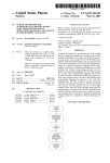
Schematic diagram of ghosting. The two legitimate events are indistinguishable from the two that are nonexistent. When measuring the
charge deposited by the tracks in a double-sided detector, it is usually possible to correlate the two X and Y measurements such that the
ghosts can be removed. . . . . . . . . . . . . . . . . . . . . . . . . . . .
Schematic diagram of the PTSM detector geometry. . . . . . . . . . .
System-level diagram of the PTSM prototype. . . . . . . . . . . . . . .
Schematic array of silicon strips on a Detector. . . . . . . . . . . . . .
Charge in a detector. I is the current from the detector while the charge
is being collected. V is the voltage at the input of the amplifier. The
voltage rises with increasing charge, and slowly decays. Here the time
scale is logarithmic. The duration of I is typically 25 ns, while the
duration of V is much longer, and depends on Ramp Camp+det . . . . .
Schematic of charge sensitive amplifier. . . . . . . . . . . . . . . . . . .
System level timing diagram for the PMFE. The FDR’s are D flip-flops
with resets, and the M2’s are two input multiplexers (see Glossary).
B CLK defines the bus cycle, which is 5 clocks long. The data is transferred over eight differential signal pairs{D7-D0} (only the first, D0,
is shown). The channel numbers which are transferred over D0 are
indicated. The channels for D1 are {14, 15, 12, 13, 10, 11, 8, 9},
D2 = D1 + 8, etc... . . . . . . . . . . . . . . . . . . . . . . . . . . . . .
Schematic of the digital region of the PMFE. An identical block handles
the odd channels for the data line. The two are multiplexed by the fast
clock at the multiplexer furthest to the right. . . . . . . . . . . . . . .
Timing diagram of setup and hold requirements. D is the input, Q is
the output, and CLK is the clock. . . . . . . . . . . . . . . . . . . . .
Photo of the Test Board. “A” shows the PMFE. The detector bias
ring is marked by “B”. If a detector is used, a window is milled out,
removing region “C”. Within “C” are the 16 external calibration capacitors. The detector bias circuitry is located at “D”. Calibration pulses
are routed through an SMB connector at “E”. The two IC’s above “F”
are the CMOS switches which route the calibration pulses to the four
buses. The IC below “G” is the AD620, which conditions the comparator threshold voltage, brought in on SMB connector “H”. All LVDS
communication is routed through the connectors on the back side of
the board at “I”. . . . . . . . . . . . . . . . . . . . . . . . . . . . . . .
Photo of the Test Board mounted on the Proto Board. The Proto
Board is denoted by “D”. The Test Board is at “C”. The output data
lines from the ROC are shown at “A”. The FPGA is in the socket at
“B”. . . . . . . . . . . . . . . . . . . . . . . . . . . . . . . . . . . . . .
vi
8
8
14
18
21
21
22
24
25
30
31
12
13
14
15
16
17
18
19
20
21
22
23
24
25
26
27
28
29
30
31
32
33
34
35
36
37
NI6534 timing diagram . . . . . . . . . . . . . . . . . . . . . . . . . . .
Photo of the Translator Board. . . . . . . . . . . . . . . . . . . . . . .
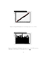
Idealized response curve to varying charge input. . . . . . . . . . . . .
Average response of a comparator with Gaussian noise superimposed
on the input charge. . . . . . . . . . . . . . . . . . . . . . . . . . . . .
Typical s-Curve for determining the gain and noise at a particular
threshold. . . . . . . . . . . . . . . . . . . . . . . . . . . . . . . . . .
Typical gain curve for a range of thresholds. In this example the gain
is 97.6 mV/fC. . . . . . . . . . . . . . . . . . . . . . . . . . . . . . . .
Typical noise values for a range of thresholds. . . . . . . . . . . . . . .
Example of an s-curve from channel 42. . . . . . . . . . . . . . . . . .
Gain curve for Channel 42. The error is artificially small due to a linear
fit to non-linear data. . . . . . . . . . . . . . . . . . . . . . . . . . . .
Analog gain map of each channel on the Test Board. . . . . . . . . . .
Noise curve for channel 43. . . . . . . . . . . . . . . . . . . . . . . . .
Chip-wide map of the noise. . . . . . . . . . . . . . . . . . . . . . . . .
A typical oscilloscope display of the averaged comparator response to
an input charge. . . . . . . . . . . . . . . . . . . . . . . . . . . . . . .
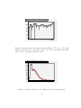
A typical gain curve from the comparator-based method of TOT calibration. The low error (.00) is artificial, and is due to a linear fit to
non-linear data. . . . . . . . . . . . . . . . . . . . . . . . . . . . . . .
A typical TOT distribution from the DAQ-based method of TOT calibration. The width of the distribution is directly related to the falling
edge of the averaged comparator output in Fig. 24. . . . . . . . . . . .
A typical TOT gain curve from the DAQ-based method of TOT calibration. . . . . . . . . . . . . . . . . . . . . . . . . . . . . . . . . . . .
Chip-wide map of the TOT gain for the range of 6-63 fC. . . . . . . .
Chip-wide map of the TOT resolution for 4 fC. . . . . . . . . . . . . .
Chip-wide map of the TOT resolution for 20 fC. . . . . . . . . . . . .
Chip-wide map of the TOT resolution for 50 fC. . . . . . . . . . . . .
A typical TOT gain curve for the charge region of .5 to 2.75 fC. . . .
The chip-wide TOT gain for the region of .5 to 2.75 fC. The errors are
artificially low. The actual error on the gain is close to .05 fµsC . . . . .
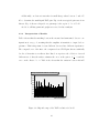
Intensity map for data taken with uncollimated 90 Sr source. Note that
channels 0 and 63 were poorly behaved, and so they were cut from the
histogram. There are two dead strips, channels 6 and 15. . . . . . . .
TOT spectrum for the uncollimated 90 Sr source measurement. . . . .
Intensity map for data taken with the collimated 90 Sr source. Note
that channels 0 and 63 were poorly behaved, and so they were cut from
the histogram. There are two dead strips, channels 6 and 15. . . . . .
TOT spectrum for the collimated 90 Sr source measurement. . . . . .
vii
42
47
49
50
52
52
55
56
57
57
58
58
62
64
65
66
66
67
67
68
69
69
72
72
73
73
List of Tables
1
2
3
4
5
Diagram showing how data corruption occurs. Event 4 was lost by the
NI6534, causing a shift in the data. For example, what is really the
time stamp of one event could be interpreted as the channel ID of the
next event. . . . . . . . . . . . . . . . . . . . . . . . . . . . . . . . . .
Diagram showing the first event to be read out. Note that all digits
are in hexadecimal format. (See the Glossary for an explanation of hex
notation.) . . . . . . . . . . . . . . . . . . . . . . . . . . . . . . . . . .
Diagram showing error handling. When an word is corrupted, an error
code is sent out, and the whole event is sent again. Note that all digits
are in hexadecimal format. . . . . . . . . . . . . . . . . . . . . . . . . .
Results of the comparator based method of TOT characterization. The
computed error on these figures is artificially low due to fitting a line
to non-linear data. . . . . . . . . . . . . . . . . . . . . . . . . . . . . .
Summary of the characterization of the PTSM system. The TOT gain
results listed are for the 5-60 fC region at the 125 mV threshold. The
noise measurements were taken without a mounted detector. . . . . .
viii
37
38
39
63
75
Abstract
“The Design, Implementation, and Characterization
of a Prototype Readout System for the
Particle Tracking Silicon Microscope”
Brian C. Keeney
The purpose of this paper is to describe the development and effectiveness of a prototype instrument with applications in radiobiology. Radiobiologists at Loma Linda
University Medical Center are studying the effects of ionizing radiation on living tissue. An instrument is needed which can correlate particle tracks with specific cells.
Using this information, detailed and precise models of the effect of radiation tissue
can be developed and adapted to cancer therapy and prevention. Engineers at the
Santa Cruz Institute for Particle Physics designed and implemented a prototype readout system. This paper describes and analyzes the characterization process of this
prototype. The preliminary results indicate that the PTSM will be able to detect
fast protons and heavy ions with excellent energy resolution and spatial resolution on
the order of a cell nucleus. These measurements will aid Radiobiologists in solving
complex problems in cancer therapy.
Acknowledgments
PTSM is a collaboration of incredible people who have given selflessly of themselves,
and have worked many long days to see the prototype to fruition. The author wishes
to thank Dr. Hartmut Sadrozinski, Ph.D., for teaching him the art and science of
instrumentation. He has treated the author with parent-like kindness, and given
him as many opportunities as possible. He is never upset when, occasionally, these
oppportunities turn into failures, but rather pushes for lessons to be learned from
them. It is only in this caring environment that learning truly flourishes. The author
also wishes to thank Dr. Reinhard Schulte, M.S., Ph.D., for introducing the author to
the concept of this microscope and educating him in the fundamentals of Radiobiology.
Engineer Ned Spencer, B.S, and Dr. David Dorfan, Ph.D., provided a spectacular
education in high speed, low noise analog design. Super Technicians Max Wilder, B.S.,
and Bill Rowe, B.S., were invaluable in teaching their craft of micro-manipulation and
electronics prototyping. They have always been willing to give freely of their time and
knowledge. Cyrus Bazeghi, M.S.C.E is an extraordinary teacher of digital design and
the Verilog Hardware Descriptive Language. Without his support both in and out
of the classroom the Readout Controller would never have reached an operational
level. Steve Petersen, M.S.E.E.,P.E has been an invaluable teacher, mentor and friend
throughout the process of implementing PTSM. His knowledge of digital systems and
their analog characteristics has given the author a rich background and understanding
of the field and of the infinite possibilities in engineering. Prof. Josh Deutsch has been
an incredible teacher and mentor for the author’s computer programming education.
The development of the analylitical software developed for this thesis would never
have been possible without his enthusiastic and expert support. The author also
wishes to thank Super Technician Forest Martinez-McKinney, who in addition to
being a wonderful friend to the author did a great deal of the detailed design of
x
PTSM. Undergraduate Research Assistant Jason Heimann, A.A., has also done a
phenomenal amount of work on the DAQ software. Without him, the PTSM would not
have a functioning DAQ. Post-doctoral Researcher Gavin Nesom, Ph.D., has provided
valuable instincts and insight into the physics of the instrument, as well as expertise
in analysis of data. Last, but certainly not least, the author thanks Chantal Keeney,
who has supported the author through good times and bad. Without her love and
her absolute disdain for mediocrity, this work would never have been finished. This
paper is dedicated to her.
xi
1
Introduction
Oncologists and radiobiologists at Loma Linda University Medical Center (LLUMC)
are studying the biological effects of radiation on living tissue for the purpose of
improving the treatment and prevention of cancer. When ionizing radiation traverses
a cell, there is the possibility of damaging the cell’s DNA, which can, in turn, adversely
affect that cell and the cells which surround it. When cells are damaged in this way,
it is possible for them to replicate uncontrollably. This process is known as “cancer”
[1]. It is important to understand how radiation affects cells both to learn how cancer
develops and to effectively stop it. To date, the standard practice in studying these
effects has been stochastic. Cell cultures have traditionally been irradiated by a microcollimated beam of ionizing radiation [2]. By knowing the average fluence and Linear
Energy Transfer (LET), an approximation of the radiation dose can be inferred. With
the development of the Particle Tracking Silicon Microscope (PTSM) it is now possible
to correlate specific particle tracks (and measurements of the LET) with individual
cells. Thus, a very precise study of radiation effects in tissue is possible [3]. This paper
will explain the need for the PTSM, define the requirements that result from these
needs, describe the development process of the instrument, and present the results of
a prototype characterization.
1.1
Biological Motivations for the Development of the PTSM
Radiation can cause damage in cells which can lead to the death of an organism [1].
This damage manifests itself in many ways [4]. The four effects which are of greatest
interest to this project are as follows:
1. Mutations: Mutations occur when DNA is ionized in such a way as to remove
or change a base pair in the DNA lattice. This results in a different genetic code
1
being interpreted by the cell. This is often to the detriment of the cell, and is a
cause of cancer [5].
2. Chromosomal Aberrations: Aberrations are mutations which are physically
manifested in the shape of the chromosomes. It is useful to study aberrations
because they are correlated to radiation dose and linked to larger physical problems in organisms [6].
3. Apoptosis: If a cell is critically damaged and is not able to repair itself, the cell
can either undergo necrosis or apoptosis. Necrosis is harmful to the surrounding
tissue, because the cell walls simply burst, releasing the contents into the tissue.
This causes inflammation and stress in the surrounding cells. When it is possible,
a cell will self destruct by apoptosis. “Stress conditions –such as starvation– as
well as damage to the cell’s DNA –resulting from toxicity or exposure to ionizing
radiation, such as ultraviolet or X-rays– can induce a cell to begin an apoptotic
process [1].” The cell gradually shuts down its internal mechanisms, and breaks
up cellular matter into pieces which are easily expelled from the tissue. This
causes little or no trauma to the surrounding tissue [7]. Apoptosis is a normal
function in organisms, and is the complement to mitosis, or cellular division.
Most diseases are caused by a malfunction in apoptosis or mitosis [1]. “It has
been estimated that 50 to 70 billion cells perish each day in the average adult
(human) because of (apoptosis),a process by which, in a year, each individual
will produce and eradicate a mass of cells equal to its entire body weight [8].”
4. Bystander Effect: The bystander effect occurs when one cell is critically damaged
by radiation. Instead of just that one cell undergoing apoptosis, several cells
surrounding the injured cell also undergo apoptosis [9].
2
1.2
Manipulation of Radiation Effects in Tissue
It is important to study radiation-induced mutations, chromosomal aberrations, apoptosis, and bystander effects, because all are mechanisms which are involved in both
the causes and treatments of cancer. It is difficult to study radiation effects in the
tissue of large organisms, because there are too many parameters to control. The best
organism for studying these effects is the one which has the fewest cells while still
exhibiting tissue-like behavior. Biologist Sidney Brenner, in the early 1960’s, found a
simple organism which had sufficient cells and was easy to study and replicate with
regularity. C. elegans is a nematode that develops 1090 cells, 131 of which always
undergo apoptosis during development [10]. Every cell is deterministic, in that it
always shows up in the same location and performs the same function. C. elegans
was the first organism to have its genome completely sequenced, making it possible
to manipulate the genetic structure of the organism. Another advantage of using the
C. elegans is that it is one mm long, which makes it barely visible to the naked eye
and easily manipulated in a laboratory setting. Additionally, C. elegans is easy and
inexpensive to produce in bulk with specific phenotypes [10]. The PTSM project uses
C. elegans in its studies of radiation effects in tissue because of these favorable traits.
The most precise way to study these effects would be by relating single particle
events to individual cells. In the past there have been no instruments able to provide
this type of measurement. The PTSM is designed to be able to resolve particle tracks
at the resolution of a cell nucleus, and to provide a measurement of the LET, which
can be used to compute the energy deposited in the cell (dose).1
1
Protons deposit energy as
dE
dX
∝ E −.77 , where X has units of
3
g
cm2
[11].
1.3
The Integration of Particle Tracking Silicon Microscope
(PTSM) Measurements into Radiotherapy
Successful radiotherapy destroys the maximal volume of cancerous tissue while seeking
to minimize damage in the patient. Radiotherapy kills cancer cells by stimulating
apoptosis and the bystander effect in the malignant tissue. The favorable mechanisms
of the bystander effect and apoptosis exhibit a saturation effect–after a certain level,
increasing the dose does not provide the same increase in effectiveness. Therefore it
is extremely important to have accurate models of how radiation affects cells.
In order to develop accurate models, large-scale, reliable, and reproducible studies
are needed. The Particle Tracking Silicon Microscope, developed by the Santa Cruz
Institute for Particle Physics (SCIPP) in cooperation with Loma Linda University
Medical Center, can help make such large-scale studies both accurate and economical. This paper will show how the prototype readout system was designed, describe
the development process of the instrument, and present the results of the prototype
characterization.
4
2
Design
In the study of radiation effects in tissue, it is essential that the location and magnitude of the damage be well known. The PTSM project correlates specific particle
tracks with the cells that they traverse. This is accomplished by subjecting a large
number of cells to a broadly collimated proton or heavy-ion beam and tracking the
energy and position of each particle with a silicon strip detector (SSD) based instrument. This section will discuss the considerations in choosing a design which would
effectively measure position and energy of particle tracks in a hostile physical environment (i.e. a saline solution in contact with electronics and repeated physical contact
with the detector itself), and the technologies (i.e. the detector type, front-end electronics, readout controller, and data acquisition hardware) that were utilized in the
development of the system.
2.1
Physical Requirements for Particle Tracking
For effective large-scale study of radiation effects in tissue, there are four physical
requirements that must be satisfied in order to obtain optimal results.
1. The spatial resolution must be fine enough to distinguish between two cells.
2. The energy resolving ability of the electronics must be fine enough to ensure
approximate quality (i.e. energy and variance) of the proton or heavy ion beam.
3. The detector must be able to withstand the presence and repeated application
of biological samples directly to its surface. This is important in ensuring the
accuracy of the position measurement by the detector, due to multiple scattering
uncertainties.
4. The system as a whole must be economically accessible to researchers in the
general radiobiology community.
5
2.2
Architecture Development
The relatively small scale of the PTSM project allows for a simpler and more compact
architecture than that of most particle physics experiments. The mass of readout and
support electronics required is minimal because only a small active area (< 1 cm2 )
is needed to study hundreds of C. elegans, very few channels (< 1000). The small
number of channels, coupled with a low event rate (< 1000 Hz), means that the data
acquisition system (DAQ) can be managed by a PC instead of a larger CAMAC or
server farm. Building a front end from discrete commercial parts is nearly impossible
due to the size of the detector and the parasitic electrical effects that scale with
increasing size. Therefore, a custom front-end chip was designed and laid out at
SCIPP by Ned Spencer. The analog blocks of the design are based on those in the
Gamma Ray Large Area Space Telescope (GLAST). The digital blocks are new, and
reflect the size of the experiment. It was decided that a Field Programmable Gate
Array (FPGA) would be used to implement the Readout Controller (ROC). FPGA’s
are arrays of Configurable Logic Blocks (CLBs) which can emulate any design that
fits on the chip. The ROC is used to do all of the digital processing of the signals
created in the detector and analog front end electronics. Because of the relatively
small data output of the detector electronics, it was decided that a commercial PCI
digital input/output card could be used, plugged directly into a PC.
2.2.1
Detector Selection
The detector selection process involves balancing the relative strengths and weaknesses
of different architectures (pixels vs. strips and single vs. double sided) and pitch to
best detect particles with a minimum of difficulty. The two main parameters which
are influenced by these choices are position and energy resolution.
Pixel detectors are made up of rectangles of doped silicon on one side of an oppo6
sitely doped wafer. There is a trace (and thus a channel) for each square. A detector
with N ∗ N pixels must have N 2 connections to readout electronics. Each connection
is ultrasonically welded to the input pads of the readout electronics.
Silicon strip detectors are made up of strips of doped silicon on one or both sides
of a doped wafer. For an N ∗ N array, there are 2N strips. This is the most striking
difference between strips and pixels. When using two sets of strips (from either two
single-sided detectors or from one double-sided detector), there are also two signals;
one from the x-side and one from the y-side. Although the signals are not the same,
they permit two measurements of the charge and thus the resolution is improved by √12 .
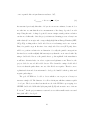
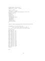
One liability in using silicon strips when the amount of charge is not precisely known
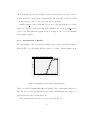
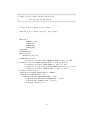
is called ghosting. Ghosting occurs when two particles traverse the detector at the
same time. Then there are four possible locations ((X1 Y1 ), (X1 Y2 ), (X2 Y1 ), (X2 Y2 ))
for only two valid hits (See Fig. 1.). This can be overcome when using a double-sided
detector, provided that the difference in the charge deposition of the two particles is
larger than the resolution. Then the two legitimate pairs (each with matching energy)
can be distinguished from the ghosts.
The PTSM project elected to use silicon strips in the instrument, because of the
savings on detector mass and complexity.
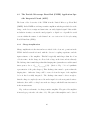
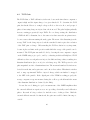
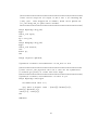
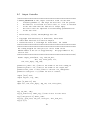
Figure 2 shows a conceptual schematic of the detector geometry. The proton beam
enters the research room horizontally. The detector is positioned with its normal axis
aligned parallel with the beam. Biological samples are deposited on the upstream face
of the detector. Particles pass through the biological samples and then through the
detector.
7
?
Y1
?
X1
Y2
X2
Figure 1: Schematic diagram of ghosting. The two legitimate events are indistinguishable from the two that are nonexistent. When measuring the charge deposited by the
tracks in a double-sided detector, it is usually possible to correlate the two X and Y
measurements such that the ghosts can be removed.
SSD
Test Board
Beam
Biological
Samples
PMFE
Figure 2: Schematic diagram of the PTSM detector geometry.
8
2.3
Front End Chip Specification
In the PTSM architecture, the front end chip amplifies and digitizes the signals coming
from the silicon strip detector SSD. It then sends the digital channel status information
to the readout controller (ROC). The major specification to be made in the Particle
Microscope Front End (PMFE) was that of the shaping time.2 Charge signals are
emitted from the detector as short bursts of current, lasting up to 30 ns [12] This
charge is deposited on the input of the PMFE, where the input capacitance and
input resistance are very large. This can be modeled as a current source charging a
capacitance, which forms a ramp in voltage. Since this happens over 30 ns, which
is much smaller than the discharge time, the effective waveform is a step function.
A preamplifier amplifies the charge on the input capacitance into a voltage which is
proportional to that charge. A shaper circuit, similar to a differentiator/integrator,
then shapes the step into a longer (in time) pulse with a quasi-gaussian shape. A
characteristic of the shaper (called the shaping time) is the time that the shaper takes
to rise from 0 to the maximum pulse height. The time during which the pulse is
above a certain threshold is a function of the input charge, which in PTSM is used
as a measurement of the particle energy. Only a very approximate measurement of
the energy is needed, enough to verify that the incident beam energy is in the correct
region. Picking the rise time is a trade off between resolution on the pulses, dead time,
and noise. If the rise time is very short, then many events can occur sequentially on one
channel, and the amplifier will be able to distinguish them as individual pulses. The
downside is that there will be poor resolution on the magnitude of the input charge
(assuming that the TOT is used as a measurement of charge, and not the height of the
pulse). By lengthening the rise time, the precision on charge measurement increases,
but different charge inputs might overlap, making two small charges look like one
2
A related term is the rise time, which is the convolution of the shaping with the collection time.
9
large one [13]. These statements assume that the sampling rate of the signal is kept
constant. PTSM chose to use a shaping time of 200 ns, and a maximum pulse length
of 300 µs, which corresponds to a maximum particle rate of ∼3 kHz for very large
charge.
10
2.3.1
Field Programmable Gate Array (FPGA) Selection for the
Readout Controller (ROC)
All digital communication in the PTSM is required to be in a logic family called Low
Voltage Differential Signaling (LVDS). It is a balanced pair of digital signals which
minimize interference in the analog portion of the microscope (See section 3.6.1). This
requirement made selection of the FPGA type very easy because at the time of part
selection, only the Xilinx Virtex 2 series had the capability of LVDS communication.
From there it was relatively simple to pick a model in the Virtex 2 series which
conformed to the speed and size requirements of the PTSM.
2.4
Data Acquisition Hardware
The PTSM project wanted a portable and economical way of transferring and storing
data from the ROC. A PCI based data input/output (DIO) card was an obvious
choice, because it can be installed in any PC. At the time of selection, there were no
affordable (<$5000) LVDS based DIO cards available. National Instruments makes
a single-ended DIO card, the NI6534. The PTSM project decided to use the NI6534
with a custom converter card to translate between CMOS and LVDS.
2.5
Conclusion
The PTSM project developed a non-standard architecture to scale existing technology
in particle physics and electronics to a new area of research. A double-sided silicon
strip detector was chosen because of the improved energy resolution and detector mass
savings over pixel detectors. An ASIC front end chip, the PMFE, was specified to
amplify, condition, and digitize the detector signals. A Xilinx Virtex II FPGA was
chosen to implement the readout controller (ROC) because of its ability to utilize the
LVDS logic family. A PCI data I/0 card, the National Instruments 6534, was chosen
11
to transfer data from the FPGA to the PC based data acquisition system (DAQ).
Having specified the architecture and functionality of the detector, front end, readout
controller, and DAQ, engineers at SCIPP constructed the PTSM.
12
3
Implementation
The implementation of the PTSM was carried out in parallel by several groups. Simultaneously the PMFE, readout controller(ROC), DIO card software, and printed
circuit board (PCB) development were undertaken. The prototype SSD is an ATLAS
single-sided “Test” detector with 50 µm pitch and is six cm long. The PMFE was
designed to interface on one side with the SSD and on the other to be bonded to
traces on a printed circuit board, called the Test Board. The Test Board is designed
to provide services (e.g. biasing and calibration signals) to the SSD and PMFE, and
to interface with the Readout Controller (ROC). The ROC is implemented on a Xilinx
Virtex II XC2V1000-FG256 Field Programmable Gate Array (FPGA). The FPGA is
mounted on a Xilinx Virtex 2 FG256 Proto Board. The Test Board mounts directly
on the prototyping board through arrays of stake headers. The ROC interfaces though
twisted pair ribbon cable to a translator board, which converts the data signals from
LVDS to CMOS. The Translator Board then connects to a PCI based DAQ card,
the National Instruments 6534, in a PC. This section discusses the methods used in
implementing the detector, front end, readout controller, and DAQ of the PTSM, and
will explain the motivation for choosing these methods.
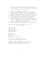
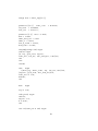
Before discussing the details of how the prototype readout system is implemented,
it helps to understand the theory of operation of PTSM. (See Fig. 3 for a system-level
diagram of the prototype readout system.) The proton beam at LLUMC has a very
well defined spill structure, with ∼100 protons spaced evenly over several hundred
milliseconds in an area of ∼100 cm2 . These spills occur every 2.2 seconds. (Heavy
ion sources are not as well defined, but the proton beam provides a reasonable baseline estimate of the particle rate.) When the DAQ is ready to start taking data, it
raises an asynchronous “start” line, which is continuously polled by the ROC. The
ROC then begins allowing events from the PMFE to be interpreted and sent to the
13
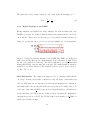
DAQ. The data from the PMFE are the time-division-multiplexed statuses of all 64
channels. The statuses are transferred over 8 signal pairs in four clock cycles at Double
Data Rate (DDR). The ROC looks for transitions in each channel and sends an event
packet (holding the channel, the direction of the transition, and the time) to the DAQ.
An event in PTSM is defined as a transition from low-to-high or from high-to-low of
a latched comparator output. Data is transferred from the ROC to the DAQ card
(National Instruments 6534) via a fully synchronous handshaking protocol (see Fig.
12, Section 3.4.4 and Source [20]). When data needs to be cleared from the RAM
on the NI6534, the NI6534 lowers an “ACKnowledge” line. The ROC buffers data
in a first-in, first-out buffer (FIFO) until the NI6534 is able to receive it again. This
should not be confused with dead time; it merely means that data is stored in the on
Figure 3: System-level diagram of the PTSM prototype.
14
board memory of the ROC until it can be transferred to the DAQ.
3
When the DAQ
is finished taking data, it lowers the “start” line. The ROC then stops taking data
and sends the last of its data to the DAQ. When the on board FIFO’s are empty, it
then raises a “done” line, which signals to the DAQ that there are no more data to
be sent. The ROC holds all data-handling state machines in reset until the “start”
line is raised again. There is currently no external triggering. The ROC sends all
transition events (channel comparators going low to high and then high to low) to the
DAQ as they occur. There is an additional function built into the controller where
the controller, when signaled by the “start” line, triggers the pulse generator 1 or 100
times. It then reads out the resulting data. This is used to calibrate the PMFE’s
analog gain and TOT gain.
3
The only dead time occurs in the PMFE, and currently lasts for 5 ns (see Section 3.2.2 for a
discussion of the dead time). For reasons that are explained in Section 3.2.2, a particle would have
to deposit ∼1.25 fC or less at exactly the right moment in order not to be detected during this dead
time. The probability of this occurring is negligible.
15
3.1
Silicon Strip Detector
The silicon strip detector is the sensor in the PTSM. When a particle traverses one
of the depleted PN junctions in the detector, a small bursts of charge is liberated,
which the front end amplifier collects and amplifies. A single-sided detector was used
for the prototype because it is identical with respect to analog characteristics while
being much easier to implement mechanically.
3.1.1
Properties of Silicon Strip Detectors
Silicon Strip Detectors (SSD’s) are arrays of diode strips. The fabrication of these
strips is usually accomplished by implanting strips of P-type silicon on N-bulk. The
diodes are back-biased (depleted) with ∼1-40 M Ω resistors connected to ground. (The
backside is biased at ∼100 V.) The strips are then capacitively coupled to the signal
connections by placing an aluminum oxide layer over the strip with a silicon oxide
layer sandwiched between the aluminum and the strip. The capacitive load seen
by the input of the amplifier varies depending on the geometry of the detector, but
typically it is 1-2 pF/cm [14].
When a particle traverses a depleted junction, it deposits a certain amount of
energy, which in turn liberates e-/e+ pairs. These charges flow up their potentials,
creating a very brief spike in current. This current is very small, and is most commonly
referred to in terms of charge, not current or voltage. A typical signal of one Minimum
Ionizing Particle (MIP) is about 25,000 electrons [15]. Assuming a 1 cm detector and
a 25 ns collection time, the average current is 160 nA. If a detector were not connected
to any other circuitry, the peak voltage would be 2.7 mV (assuming 1.5 pF). When
an amplifier is connected to the strip, the effective capacitance becomes much higher,
decreasing the voltage.
Since SSDs are depleted in normal operation, there is very little quiescent current,
16
typically ∼1
nA
.
cm2
This is an extremely important parameter because of the signal
size. What in other applications would be considered to be negligible variations in
bias current translate to potentially crippling shot noise at the output of the detector
√
(inoise = 2qibias B, where q is the charge of an electron and B is the bandwidth in
Hz [16]. The shaping time of the amplifier is a reasonable measure of the bandwidth.
The equation for the noise can be rewritten in terms of noise charge by substituting
this value:
qnoise =
q
2qibias Tshaping
(1)
Using the previous values, and a shaping time of 300 ns (that of the PMFE) the noise
is 60 electrons, which is very small when compared to one MIP. Another important
parameter of a SSD is the capacitance. The effective input capacitance of the amplifier stage must be much larger than the detector capacitance, because otherwise the
amplifier will appear as a high impedance node, which will cause a long shaping time
before the shaping stage, which is undesirable from the point of shot noise.
The spacing between adjacent detector strips, or pitch, is a trade-off between
resolution and the number of channels. Obviously having many strips improves the
resolution, but it adds cost, complexity, and mass to the system. More channels are
needed, which translates to more bonding pads on chips, more power consumption,
and in some cases active cooling. All of this is difficult and costly. Conversely, one
large strip covering the active area will capture all the charges, and will be inexpensive,
but will tell nothing of the position of particle tracks and have large capacitance. One
first needs to decide what resolution one can live with, and then pick a detector pitch.
The resolution is not the pitch, as one might assume:
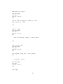
There is a very good probability (near 100%) that if a particle traverses a strip, or
any point before the half way point to the adjacent strip, that a hit will be registered
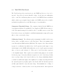
(See Fig. 4). This assumption gives rise to a box probability distribution,
17
P (x) =
0
x < W/2
1 −W/2 < x < W/2
0 x > W/2
where W is the strip pitch, and the origin is at the center of the pitch. By symmetry,
< x >= 0
(2)
One can derive the standard deviation, σ, which is the positional resolution of the
detector.
2
σ =
Z
W
2
−W
2
x2 − < x >2 dx
R
W
2
−W
2
(3)
P (x)dx
v
u x3 W −W
u ( ,
2 )
σ = t 3 W2 −W
(4)
L
σ = √ = .289L
12
(5)
x(
2
,
2
)
Therefore,
This result means that for
√2
12
of all events, the particle will have landed within
√1
12
of the center of the strip. For the Silicon strip detector to be able to resolve whether
Figure 4: Schematic array of silicon strips on a Detector.
18
or not a particle hit a 20 µm diameter nucleus to 50%,
Lmaximum = 10−5 m ∗
√
12 = 35 µm
(6)
As was stated previously, this value of 35 µm is a worst case estimate, because it does
not take into account that there is a measurement of the charge deposited on each
strip. Using the ratio of charge deposited between 2 strips, actual position resolution
can far exceed this value. Since the project is interested in using protons or heavy ions
with relatively low energies and correspondingly high Linear Energy Transfers (LET,
dE/(ρdX)), working with a double sided detector is advantageous for two reasons.
First, if a particle stops in the first of two single sided detectors (X-Y pair), there
will be no position resolution in one dimension. Secondly, the particle emerges from
the first detector with a slightly different trajectory than the one it entered with. By
using a double-sided detector, the particle has to go through half of the mass that it
would have otherwise had to in order to register as a legitimate event. Therefore, the
project decided to use a double sided detector. The downside to using a double sided
detector is that the pulses that come out of the N side are negative. Therefore, more
sophisticated front-end electronics must be developed to handle both the positive and
negative pulse shapes.
The goal of PTSM is to be able to detect whether or not a proton or heavy ion
traverses a single cell. The diameter of a cell is ∼10-20 µm, which necessitates a pitch
of ∼35 µm. The detector that best fits the needs of the PTSM for prototyping, is a
SINTEF double sided SSD with 50/80 µm pitch (P/N) and an active area of 2.4 cm
X 1.2 cm.
4
As the project matures a custom detector with a smaller active area and
finer pitch will be developed.
4
PTSM uses only .64 cm X 1.2 cm.
19
3.2
The Particle Microscope Front End (PMFE) Application Specific Integrated Circuit (ASIC)
The heart of the electronics of the PTSM is in the Particle Microscope Front End
(PMFE). In the PMFE are 64 charge-sensitive amplifiers and shapers which detect the
charge on the detector strips and turn it into an easily digitized signal. Pulse-widthmodulation circuitry converts the analog signal to a digital one. A parallel-to-serial
converter shifts the status of each channel out over 8 wires in 4 clock cycles using
Double Data Rate (DDR).
3.2.1
Charge Amplification
Charge amplification is the first and most critical of the electronic operations in the
PTSM. An RC network is formed with the detector’s coupling capacitance and the
input resistance of the amplifier. This RC is typically much larger than the 25 ns
collection time. As the charge is collected the voltage at the front end rises linearly.
The discharge time is much larger than this charging time (as much as several thousand
times greater, due to Rinamp Cinamp +det ) [12]. (Refer to Fig. 5 for a logarithmic
representation of the pulse shapes.) This discharge time must be greater than the
shaping time. Otherwise charge will be removed from the input of the amplifier
before it has been fully integrated. The discharge time must be short enough so
that the charge is completely removed from the input before the next particle arrives.
Otherwise, there will be overlap between the two charges, which will cause inaccuracies
in the measurements.
Fig. 6 shows a schematic of a charge-sensitive amplifier. The gain of the amplifier
is inversely proportional to the value of Cf . The gain of this amplifier can be derived
20
as follows: The charge on Cf will be the same on both sides. Therefore
Qi = Qf = Cf ∗ Vout
(7)
I
V
ln(T)
Figure 5: Charge in a detector. I is the current from the detector while the charge
is being collected. V is the voltage at the input of the amplifier. The voltage rises
with increasing charge, and slowly decays. Here the time scale is logarithmic. The
duration of I is typically 25 ns, while the duration of V is much longer, and depends
on Ramp Camp+det
VOUT
DET
Qin
C_F
Figure 6: Schematic of charge sensitive amplifier.
21
The gain is the voltage output compared to the charge input. Rearranging eq. 7,
Gain =
3.2.2
Vf
1
=
Qi
Cf
(8)
Digital Topology in the PMFE
Having amplified and digitized the charge impulses, the next and final task of the
PMFE is to register the digitized channel statuses and transmit them to the Readout Controller. This section describes the process by which 64 channel statuses are
mapped to specific time slices over 4 clock cycles and multiplexed onto 8 signal lines.
Figure 7: System level timing diagram for the PMFE. The FDR’s are D flip-flops
with resets, and the M2’s are two input multiplexers (see Glossary). B CLK defines
the bus cycle, which is 5 clocks long. The data is transferred over eight differential
signal pairs{D7-D0} (only the first, D0, is shown). The channel numbers which are
transferred over D0 are indicated. The channels for D1 are {14, 15, 12, 13, 10, 11, 8,
9}, D2 = D1 + 8, etc...
Front End Latches The output of the shaper is fed to a comparator with a threshold voltage. A rising edge from the comparator feeds to the input of an asynchronous
set/reset (SR) latch. In one chip, there are 64 front-end amplifiers, 64 comparators,
and 64 SR latches. At a specific time in the bus cycle (a bus cycle consists of five clock
cycles and begins with a B CLK) on the front-end chip the statuses of all latches are
checked and then reset. The frequency of this operation determines the quantization,
and thus the precision, on TOT. The TOT is defined as the number of B CLK’s for
which a given channel is high.
22
Parallel to Serial Data Conversion
One approach to transferring the channel
information to the outside world would be to have signal pair for each channel. This
would work, but it would make the size of the chip very large given the pitch of the
detector. It also would require a lot of power to drive each wire, which in turn would
cause heating, noise, and power supply problems. The opposite approach would be to
serialize the data, which is a technique where each channel gets its own slice of time
on one wire [17]. This technique, called Time Division Multiplexing (TDM) is very
inexpensive because there is only one data output pad on the chip, which can make it
very small. When one does this the effective data rate is decreased by
1
Nchannels
when
compared to the parallel technique. The technique used by PTSM is a compromise
between the two, appropriately named serial/parallel. The PMFE serializes groups of
8 channels, cutting the wire count by a factor of eight. It also uses a technique known
Double Data Rate (DDR), where data is read out on both the rising and falling edges
of the clock. For instance, if the clock is running at 100 MHz, it is possible to read out
200 megabits of data per second per wire. This technique is accomplished by using a
pair of positive and negative-edge triggered flip-flops together for each data line. This
means that the statuses of two channels can be read out in one clock cycle, one on the
rising edge and one on the falling edge. For example, channel 0 could be valid during
the rising edge of the clock cycle and channel 1 then could be valid during the falling
edge of the clock cycle. This places higher demands on the system, because data must
be latched twice as fast, cutting all slack time in half. Figure 7 is a timing diagram of
how data is clocked out from the front-end chip. Note that on every signal line there
are two channel statuses transferred for every clock cycle.
Below (Fig.8) is a schematic of part of the digital section of the front-end chip.
This block repeats 16 times in the chip (8 for the even channels, 8 for the odd), and
is basically 4 SR latches, and a four-bit shift register. Note the signal called B CLK.
23
This is a reset pulse, which determines the bus cycle. The time during which B CLK
is high before clock is high loads the shift register. The time when the two signals are
overlapping clears the SR latches. When B CLK falls, the shift register stops loading
and begins to shift out the data on each edge. The data is clocked out over four cycles,
followed by one cycle of dead time.
Dead Time
When both the B CLK and CLK are high (see Fig. 7, the front end
latches are in reset. If comparator goes high during the reset, and continues to be high
Figure 8: Schematic of the digital region of the PMFE. An identical block handles
the odd channels for the data line. The two are multiplexed by the fast clock at the
multiplexer furthest to the right.
24
after the reset falls (5 ns at 50 MHz), the latch will go high, as it should, and the event
will be recorded. If the comparator goes high and then low (where the peak of the
pulse just grazes the threshold voltage) during this brief window, the event will not
be recorded. At a gain of 120
mV
fC
and a threshold of 120 mV, this would correspond
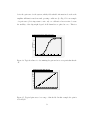
to a ∼ signal, which is highly unlikely for a legitimate particle [26].
Proper Acquisition of Data From the PMFE
When transferring data, it is
important that the data is valid during a clock edge. If the data is changing while
the clock is changing, the value latched by the readout controller will be either the
data from before or after the transition, but it will be impossible to know which. (See
figure 9.) The time during which the data must be stable before the rising edge of the
clock is called the setup time and the time after the rising edge is called the hold time
[17]. Since data is being transferred at DDR, it is especially important that the setup
T_Setup T_Hold
CLK
D
Q
Figure 9: Timing diagram of setup and hold requirements. D is the input, Q is the
output, and CLK is the clock.
and hold times are obeyed. Failure to latch the data correctly means that channel
identities will be mis-matched, which is disastrous for this instrument.
25
3.3
The PTSM Test Board
The Test Board provides several services to the PMFE and detector, if one is being used. It provides a low-noise threshold voltage. It also has some rudimentary
logic to control how calibration pulses are routed to the PMFE. It has several filters
which condition power signals being brought to the PMFE, and provides a durable
mechanical test platform for several different types of experimentation.
Comparator Threshold Voltage The comparator threshold in the PMFE is set
by an American Reliance Programmable Power Supply via GPIB. It has accuracy to
1 mV. The signal is transported via RG-58 cable to an SMB connector on the Test
Board, where it is processed further by an AD620 instrumentation amp and low pass
filter to reduce errors in the voltage.
Calibration Control
The calibration pulse is transmitted via RG-58 cable from a
LeCroy 4145 to an SMB connector on the Test Board. There it is terminated and
routed through four CMOS switches (ADG-436). The output of each of these switches
is passed to a calibration bus which feeds to 50 fF capacitors at the input of every
fourth channel on the PMFE. Additionally, there are 16 2.2 pF capacitors mounted
where a detector would otherwise be. Wires can be bonded from these capacitors
to the amplifier inputs. These capacitors are switched using jumpers on four stake
headers in groups of four (four calibration capacitors for each of four buses). In this
way a very large charge can be injected with very low voltages, minimizing channelto-channel crosstalk at the inputs of the amplifiers. For example, injecting 20 fC with
the external capacitors (2.2 pF) requires only 91 mV, while the internal capacitors
(50 fF) require 400 mV to inject the same charge. The maximum rate of change of
voltage between two conductors, where one is being driven and the other is quiescent
26
is [18]:
∆V
dV
=
dT
Tr
(9)
Where ∆V is the difference in voltage between a logic 1 and 0, and the rise time, Tr ,
is [18]:
Tr = 2.2Zo C
(10)
Zo is the characteristic impedance of the driving conductor, and C is the load capacitance. The maximum current crosstalk is derived below:
Q=C ∗V
(11)
dQ
dV
=i=C
dT
dT
(12)
(13)
Icrosstalk = Cmutual
dV
dT
(14)
Where Cmutual is the parasitic capacitance between channels, and Ccalibration is the
capacitor through which charge is injected. The total current crosstalk in terms of
capacitance is then:
dQ
∆V
= Cmutual
dT
2.2Zo Ccalibration
(15)
which clearly shows that there are gains to be made by both increasing the capacitance
and decreasing the voltage.
The total crosstalk savings can be seen by comparing the two crosstalk errors for
an equivalent amount of charge input.
Q1 = Q2
27
(16)
C1 ∗ V1 = C2 ∗ V2
(17)
V2
C1
=
C2
V1
(18)
∆V1
Cmutual 2.2Z
iC1
o C1
=
∆V
iC2
Cmutual 2.2Zo2C2
(19)
iC1
=
iC2
∆V1
C1
∆V2
C2
=
V1 C2
V2 C1
(20)
Substituting eq. 18 into 20, the total crosstalk savings is (C1 = 50f F , C2 = 2.2pF ):
iC1
50 f F 2
C2
) = 516.5 ∗ 10−6
= ( )2 = (
iC2
C1
2.2 pF
(21)
This means that the crosstalk for the equivalent charge is reduced by a factor of
nearly 2000 when using the external calibration capacitors. For large charge inputs,
the external capacitors are essential.
28
Biasing
The Test Board also routes and filters the detector bias voltage, as well as
several other bias currents and voltages for the PMFE.
FPGA Interface
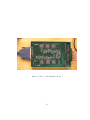
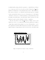
The Test Board (See Fig. 10) was designed to mount directly
onto the stake headers of a Xilinx Virtex 2 FG256 Proto Board (See Fig. 11 for a
photo of the Proto Board.), which is a prototyping workstation for Xilinx FPGAs. The
Proto Board provides a variable frequency clock, the connection to a PC for design
downloading, and arrays of stake headers leading directly to the FPGA input/output
blocks. The Test Board uses a system of female row headers on the back side of the
PCB, such that it sits directly on top of one stake header array.
3.4
The Readout Controller
There were very few requirements placed on the design of the Readout Controller
(ROC). In fact, the only two requirements on the structuring of the ROC are at
the interfaces to the PMFE and the NI6534. The front-end chip requires a very
specific clocking structure (Fig. 7), and the data acquisition card follows a strict fullysynchronous handshaking protocol. Since there is no buffering or handshaking between
the ROC and the front-end chip, it is essential that the ROC have the capability to
send the front-end clock and B CLK, to know when data would be arriving back at
the ROC, to latch it correctly, and to process it quickly enough so that there are no
overruns.
There is a delay between the time when the front-end clocks are sent and when
data is received at the ROC, due to the propagation delay in both the wires and chips
(See Eq. 22).
Tdelay =
1 √
ps √
∗ ² ∗ l = 84.7 ∗ 4.5 ∗ l
c
in
(22)
c is the speed of light, ² is the dielectric constant (FR4 PCB is 4.5 [18]), and l is the
29
distance of the PCB trace. It is necessary to be able to adjust the phase between the
clock which latches the data in the ROC and the clocks that are sent to the front-end
chip so that correct data can be acquired. By looking at the front-end DDR registers,
one can vary the phase until the correct data is latched (i.e. data associated with a
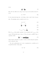
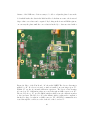
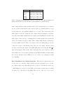
Figure 10: Photo of the Test Board. “A” shows the PMFE. The detector bias ring is
marked by “B”. If a detector is used, a window is milled out, removing region “C”.
Within “C” are the 16 external calibration capacitors. The detector bias circuitry
is located at “D”. Calibration pulses are routed through an SMB connector at “E”.
The two IC’s above “F” are the CMOS switches which route the calibration pulses
to the four buses. The IC below “G” is the AD620, which conditions the comparator
threshold voltage, brought in on SMB connector “H”. All LVDS communication is
routed through the connectors on the back side of the board at “I”.
30
positive edge is always latched correctly, and data associated with a negative edge is
always latched correctly on a negative edge). A feature of the FPGA called a Digital
Clock Manager (DCM) is used to implement this function. A DCM is a physical
device in the FPGA, which can vary phase, manipulate frequency, change duty cycle,
and implement other functionalities. There are eight DCMs in the XC2V1000 [19].
The other requirement placed on the Readout Controller is that it be able to interface with a National Instruments PCI-6534. The 6534 is a Digital I/0 (input/output)
card with 32 single ended, bidirectional data lines. In addition, it has a bidirectional
clock, and two handshaking lines, ACK (acknowledge, or ready for data), and the
REQ (request, or ROC ready to send data). The 6534 has several modes of operation. In the mode used, Burst Mode Handshaking (more commonly known as Fully
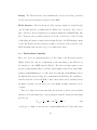
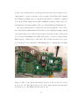
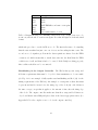
Figure 11: Photo of the Test Board mounted on the Proto Board. The Proto Board
is denoted by “D”. The Test Board is at “C”. The output data lines from the ROC
are shown at “A”. The FPGA is in the socket at “B”.
31
Synchronous Handshaking), the ROC sends the clock to the 6534 and waits for ACK
to be high, signaling that the 6534 is ready to accept data. When the ROC wants
to send data, it raises REQ and places data on the bus. On the rising edge of the
clock, the data is latched by the 6534. If ACK falls, it means that the data will not
be latched.
These requirements placed on the interfaces of the ROC are the only constraints
placed on the architecture. The rest of the design is flexible, and is a compromise
between speed, gate count, and data compression.
3.4.1
Timing Services
As has been stated previously, it is very important that data be latched from the
front end chip at the correct times, otherwise channel statuses will be mislabeled, and
some statuses will be lost altogether. To remedy this, there are two parameters which
must be constant every time that the ROC is reset. The phase between the front
end clock (FE CLK) and the main clock (CLK) must be aligned such that the rising
edge of CLK is framed squarely by the rising and falling edges of the even channel
data. This is referred to as correct phasing of the clock. Secondly, the front end
state machine must start so that when it latches its first positive channel, valid data
is present from the corresponding channel on the front end chip. This is referred to
as correct framing of the clock. If everything starts deterministically after the falling
edge of the reset pulse, this is a trivial task. However, the DCMs are analog devices
which take varying amounts of time to lock onto their clock signals. Since two DCMs
are cascaded in this design, one must wait until both DCMS are locked onto their
frequencies. Secondly, the DCM outputs glitch for the first 10 clock cycles after the
LOCKED signal goes high, so a delay must be inserted (using a counter) to remove
the possibility of synchronizing incorrectly on the glitches. Additionally, there is a
32
variable phase between FE CLK, CLK DATA, and CLK. All of the state machines
in the ROC are clocked with CLK, but need to start with respect to CLK DATA. In
the case of a state machine glitching and needing to restart, the signal must also be
recurring, i.e. a step function cannot be used. Therefore, a clock which is 1/5 the root
clock frequency (used to make the B CLK pulse) is used to provide the synchronization
pulse to SER 2 PAR.5 The clock tree source code can be found in appendix B.1.
3.4.2
De-serialization of PMFE Data
The first step in handling the data is to decode it from eight channels over eight wires
to 64 registers, each holding the status of a particular channel. Since it takes five
clock cycles (4 for readout and one reset cycle) to read in all 64 channels, the 64-bit
register is updated every five clock cycles. The buffering of the 64 bits has to begin
at the correct time in the bus cycle. If it doesn’t, some of the channels will be missed,
and the rest will be incorrectly mapped, due to misalignment of the bus cycle and the
latching cycle. This synchronization has to happen on startup. The state machine
uses a clock from which that B CLK is derived, and triggers a counter after the rising
edge of that clock. The state machine begins latching data when the counter has
delayed by a set number of fast clocks. The exact number of clocks is found by trial
and error using jumpers on the Proto Board. As stated previously, it is desirable to
run the front-end as fast as possible because the precision on TOT is proportional to
the sampling rate. Therefore, this de-serializing block of the ROC should be organized
to run as fast as possible. One way to ensure a high running speed is to arrange the
logic blocks very tightly. This way, there will be very low skew (See Glossary), even
though the regular routing layer is used. Additionally, it is possible to latch the data
in the input/output blocks (IOBs). IOBs are a slightly different type of CLB, which
5
The root clock is the fastest clock on the FPGA, used to run most of the state machines and
services in the ROC.
33
additionally contain the physical pin connected to the outside world. The signal from
the front-end chip first comes through the IOB before traveling to the rest of the
ROC. The IOBs have two flip-flops, one of which can be configured as a negativeedge-triggered flop. Therefore, a very elegant way of latching both the positive edge
data and the negative edge data is to configure the IOB to grab both edges using its
two flip-flops, one of which is configured in negative-edge-triggered mode.
At that point there is no need to keep the negative edge data in negative-edgetriggered flip-flops, so the change to one time domain can be made immediately to only
positive-edge-triggered flip-flops. This reduces the complexity of the design, which
therefore reduces the possibility of mistakes. Four 16-bit flip-flops are linked in series,
and continually latch and shift the data from the DDR IOBs. This configuration
is known as a shift register or pipeline, because data continually shifts through the
flip-flops (See Appendix B.2 for the complete de-serialization source code.)
At any one time there are four registered time slices from the front-end chip being
shifted through the pipeline. If one were to look during the correct clock cycle, one
would see the statuses of all 64 channels at the outputs of the flip-flops. The outputs
of these flip-flops are then wired to a single 64-bit flip-flop with a clock enable. At the
appropriate time in the bus cycle, the clock enable on this 64-bit register is raised,
and the status of all 64 channels is captured. A strobe called “data ready” signals to
the subsequent stage that the data is present and stable, and will continue to be for
four clock cycles. The following stage synchronizes off this pulse, but does not use it
at any other time, because the signal is periodic.
3.4.3
Buffering the Data/Zero Suppression
It is important to compress data as quickly as possible, because every stage where
the data is not compressed must have a higher throughput than would otherwise
34
be necessary. Delaying data compression translates directly into cost and difficulty.
PTSM uses a blend of zero and data compression. The output from the PMFE is the
multiplexed status of all channels over one bus cycle even if a channel is inactive, and
has been for several seconds, the PMFE will continue to send its status. Therefore,
the first operation that is done on the data after de-serialization is to store information
about a channel only when it transitions from low to high or high to low. Since there
are 64 channels to perform this operation on, and only four clock cycles in which to
do it, parallel processing techniques must be used. It makes sense that the largest
number of channels able to be monitored by a state machine over four clock cycles
is four, because it needs a clock for each comparison. “Channel server.v” is a state
machine with one init/synchronization state and four monitoring states. During the
init state, Channel Server monitors the “data ready” line of the serial to parallel
conversion, and launches into the first comparison state just after the 64-bit channel
status bus is updated. It has a four bit register which stores the last known state
of the channels. During the first monitoring state, it compares the zeroth bit of its
input bus with the zeroth bit of the channel status register. If the two are different,
it raises the write enable of a FIFO, which stores a two bit channel ID, the transition
(1 for 0-to-1, 0 for 1-to-0). At the moment that the FIFO writes the event, the state
machine is already in the next state, comparing the status of the next channel. As an
example of typical operation, consider a case where channel 15 goes high for 2 µs at
time 10 (0X0000000A).6 The bus clock period is 100 ns, so there will be 20 full checks
of channel 15’s status before it goes low. At the first presence of a 1 in the data bit
for channel 15, the state machine will write [11,1,0000000A] to the FIFO. When the
channel falls at time 30 (0X0000001E), the state machine will write [11,1,0000001E]
to its FIFO.
6
The state machine itself sees channel 15 as channel 3. The first state machine truly has channels
0 through 3, the second state machine has 4,5,6,7 which it sees as 0,1,2,3, and so on.
35
At this point in the design there are 16 channel monitors each having a FIFO
to which it writes data. These state machines collectively monitor all 64 channels.
“Fifo server.v” monitors the status of each of the 16 FIFO’s, and reads each of their
contents into a master FIFO, which is in turn emptied by the output controller. The
different channels in the small FIFO’s are distinguished with an additional five bit
channel tag (5 bits + 2 bits in the FIFO= 128 channel IDs). The FIFO’s are each
equipped with “some”, “many”, and “full” flags. The “some” flag is true whenever
the FIFO is not empty. The “many” flag is true whenever the FIFO is half or more
full, and the “full” flag is true when the FIFO is full. When none of the “many” flags
are true, the server loops over each FIFO, reading out a single event if there are any
to be read. If one or more “many” flags are high, the server skips over any FIFO’s
which only have a “some” flag, and completely empties those which have a “many”
flag. If there is more than one “many” flag, the server will empty the first one that it
finds and skip over “some” FIFO’s until it finds and empties the remaining “many”
FIFO’s. The “some” FIFO’s are still read out after all “many” FIFO’s are empty, and
no data is lost unless a FIFO is overrun.
3.4.4
Output controller
Inserting a FIFO between the input and output stages effectively divides them into
distinct blocks which are not synchronized. If the input block has no data, it writes
nothing to the FIFO. If the FIFO is empty, the output controller waits in an idle
state, ready to send data to the DAQ. The output controller performs four main
tasks: it reads data from the FIFO when the FIFO is not empty, it divides the data
up into packets that the NI6534 can handle, it sends these packets to the NI6534, and
performs error handling if there is a problem with either the FIFO or the NI6534. It
performs all of these tasks in one finite state machine called output ctrlr.v (Appendix
36
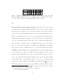
Correct
Error
Result
1
1
1
2
2
2
3
3
3
4
X
5
5
5
6
6
6
7
7
7
8
8
8
9
Table 1: Diagram showing how data corruption occurs. Event 4 was lost by the
NI6534, causing a shift in the data. For example, what is really the time stamp of
one event could be interpreted as the channel ID of the next event.
B.7).
Packet Creation in the Output Controller
The NI6534’s data bus is 16 bits
wide, while the event length in the ROC is 40 bits.7 Therefore it is necessary to package
the data into three packets of 10, 15, and 15 (the 16th bit of the bus is reserved for
error codes). These packets must then arrive in succession at the NI6534 in order for
them to be reassembled into the correct event. A missed packet corrupts all of the
data in the file following the corruption. (See Table 1.) Therefore, it is important to
send out codes that subsequent software can look for to synchronize with the start of
an event. It is too wasteful to send a code signaling the start of every event. Rather,
an error code is sent out when the state machine starts (0XAAAA), any time that
there is an error in the communications protocol between the ROC and the NI6534
(0XBBBB), and if the FIFO gets overrun (0xCCCC).8 Note that the 16th bit is high
for all of these words.9 Since it is possible for the time stamp to have any of these
values in both the high and low two byte packets, the 16th bit is reserved only for
error codes, and the 40-bit data packet is split into 10, 15, and 15 bit packets. In this
way it is impossible for a time stamp to appear to be an error code. During normal
operation, the output controller reads the FIFO by strobing the FIFO RD port of the
FIFO. This causes a new event to appear at the FIFO output. The output controller
7
There are 7 bits for 128 channels or 2 PMFE’s, 1 transition bit, and 32 time bits for roughly 7
minutes of operation without a repeat time stamp
8
For a brief description of hexadecimal notation, see Appendix A.
9
A word is a string of digital numbers
37
Data Bus
AAAA
0123
4567
89AB
CDEF
Interpretation
Start Error Code
Bits [15:0] of first event
Bits [31:16] of first event
Bits [47:32] of first event
Bits [63:48] of first event
Table 2: Diagram showing the first event to be read out. Note that all digits are in
hexadecimal format. (See the Glossary for an explanation of hex notation.)
then loads the 40-bit word into its shift register. As it loads the 40-bit word, it inserts
two zeros between bits 14 and 15 and between 28 and 29, so that the high bit of every
16-bit packet is zero, in compliance with the error code rule. The lowest 16-bits of the
shift register are also the output bits. The output controller attempts to send these
bits. After successfully sending them, the output controller shifts the contents of the
shift register down by 16 bits, overwriting the word that was just sent out with bits
[31:16], and leaving bits [41:32] empty. This continues until all three packets have
been successfully sent (See Table. 2). If there is an error during this process, the
event is not dropped. After having serviced the error, the output controller reloads
the same event from the output of the FIFO (this time not strobing the FIFO RD
line), and attempts to shift out the entire event again. The only exception to this is
when ACK is low for a long time, in which case the FIFO will fill up, in turn causing
the readout controller to issue a FIFO error code. See Fig. 3 for a diagram of normal
error handling.
Error Handling in the Output Controller
When an error (such as those in-
troduced above) occurs, the output controller loads the appropriate error code into
the output register, and waits until it is able to send it to the NI6534. In the case
of ACK falling (see section 3.5.1), an ACK error is registered when ack is low during
the rising edge of the fast clock (50 MHz). There are two other error codes, both of
38
Data Bus
AAAA
0123
4567
BBBB
0123
4567
89AB
Interpretation
Start Error Code
Data
Data
ACK ERROR–send same event again
Data
Data
Successful transfer of event
Table 3: Diagram showing error handling. When an word is corrupted, an error code
is sent out, and the whole event is sent again. Note that all digits are in hexadecimal
format.
which take precedence over the ACK error code. The first is the start code, signaling
that the state machine has just come out of reset, and is sending its first event. The
second error code signals a problem in the data acquisition software. It is the FIFO
overrun word, which means that so much data came into the ROC that the FIFO
couldn’t store it all, and that it had to be erased. If the DAQ is working properly,
this condition should never be encountered.
Handshaking in the Output Controller
The NI6534 has specific setup- and
hold-time requirements that must be obeyed for data transmission to be successful.
(See Fig. 12 for an example of fully synchronous handshaking and Ref. [20] for the
timing requirements of the NI6534.) An example of a setup time is that data must
be present and stable four ns before the rising edge of the clock [20]. A hold time is
the same concept, except that it applies to the amount of time after the rising edge
of the clock. The output controller makes sure that these setup and hold times are
obeyed, and that it raises REQ and places data on the bus at appropriate times. (See
Appendix B.7 for the complete source code for the output controller.)
39
3.4.5
Calibration Controller
Originally it had been planned that the DAQ PC would control both the readout of
data with the NI6534 and the injection of charge for calibration pulses via GPIB. This
proved to be a problem because the synchronization between the two buses is limited
to 15 ms in either direction.10 This low and unpredictable rate limited data gathering
to a few hundred Hertz. It was decided that it would be much better to have the
FPGA trigger the pulses, and to add two handshaking signals to the system. Extra
digital lines on a NI6703 Digital to Analog Converter (DAC) card were converted to
LVDS on a lab-built PCB. One line is from the DAQ to the ROC, and the other is
from the ROC to the DAQ. An asynchronous handshaking protocol is used to signal
the FPGA to start accepting data. The ROC raises its line when it is finished pulsing
and reading out its data to the DAQ. The two lines are named “start” and “done,”
respectively. “Pulse Handler.v” serves as a master controller, and handles the reset
states of the zero suppression, FIFO, and output controller blocks. The master reset
line still controls the clock tree, which in turn controls the resets of the serial to parallel
conversion and calibration controller blocks. When Pulse Handler receives the start
strobe, it lowers the reset line of the zero suppression, FIFO, and output controller
blocks. It then waits for them to synchronize and become idle. After this wait, it
sends a trigger to the pulser via an LVDS line. It then waits 409.6 µs for the analog
electronics to fully integrate the charge. It then waits until all of the inputs are low,
the FIFO’s empty, and the output controller is idle. Then it polls a jumper on the
Proto Board. If the jumper is set (i.e. the value is 0), then it repeats this process 99
times. If the jumper is not set, or if the counter that counts the number of pulses is
at 99 (100 pulses sent), the controller forces the blocks under its control to reset. It
then raises the “done” line and waits for the DAQ to lower the “start” line. Once the
10
15 ms is an empirically derived and very approximate number. It is, however, several orders of
magnitude above that which is needed, making a precise measurement unnecessary.
40
“start” line is low, the controller waits for the next “start” in the idle state. There
is another jumper which can be set to have the ROC run in a “normal” mode, where
the ROC begins taking data from the PMFE when the “start” line goes high, and
stops taking data when it is lowered. This mode is used for taking noise data with no
calibration pulses or calibration data with a radiation source. There is no trigger for
particle events; (zero suppressed) data is simply read out to the DAQ as it comes in
from the PMFE.
3.5
The NI6534 Data Acquisition PCI-Card
The PTSM project decided that it was not cost effective to design and build a custom
DAQ card, and instead purchased a ready made card with existing driver software.
The NI6534 is capable of transferring up to 32 bits at up to 20 MHz for short periods
of time, which is a higher throughput than Firewire or USB 2.0, yet with a much
simpler protocol.
3.5.1
Fully Synchronous Handshaking
The National Instruments PCI-6534 is a 5V CMOS Digital input/output PCI card
with 32 bidirectional data lines and six control lines. It is capable of acquiring data in a
number of protocols, the most reliable and robust of which is called fully synchronous
handshaking (FSH). One can make an analogy to FSH with a water balloon toss.
Nobody wants to drop the balloon. Every throw of the balloon counts. If a thrower
wants to initiate a toss, (s)he makes sure that the sender is ready by calling out. If
the sender is not ready, nothing happens; otherwise the toss occurs. The same is true
of FSH. The PC (the receiver) has control of a line called ACKnowledge. Any time
ACK is high, the ROC is free to send data. The ROC might not always be ready,
however, so it has a control line called REQuest. When ACK is high and REQ is high,
41
the PC will latch whatever is on the data bus at the next rising edge of the clock sent
by the ROC. Figure 12 shows the timing diagram for this process. Note that the card
is limited to certain period, setup, and hold time constraints that must be obeyed in
addition to the handshaking protocol [20].
Figure 12: NI6534 timing diagram
3.5.2
Readout Software
Getting the data latched into the NI6534 is only half of the process of data acquisition.
Events are 40-bits wide in the ROC, but the data bus is only 16-bits wide (32-bits
total, 16 are reserved for another FPGA).11 This means that 3 packets need to be
made from the one 40-bit event. Using these error codes and knowledge of the packet
structure, University of California, Santa Cruz physics undergraduate Jason Heimann
wrote a C++ program which interfaces to the card. The program, PTSM CALIB uses
National Instruments C libraries to initialize the NI6534, to initiate read operations
by the card, and to read the card’s RAM. The program then parses the file, looking for
11
There are 32 bits for the time, seven bits for the address, and one bit for the transition.
42
error codes and reassembling the packets. When an error code is found, the current
event that is being parsed is thrown out, and the first word after the error code starts a
new event. It then turns this data into separate events for each channel that is active.
Finally, using ROOT libraries [21], the data is stored with very high compression
(∼X30) into an NTuple. This NTuple is then easily transported and analyzed on
other machines. (For the source code to PTSM CALIB, see appendix E.)
3.6
The PTSM Translator Board
One drawback to using the NI6534 is that it cannot interface with LVDS logic levels.
A translator card was designed to make communication possible between the ROC
and the NI6534.
3.6.1
Differential signaling
The Low Voltage Differential Signalling family (LVDS) is used extensively in PTSM.
At first it is not easy to comprehend why it would be used. It is differential, so it uses
twice the wires; it is expensive (more than 10 times that of CMOS); and one cannot
directly interface it with most equipment or parts.12 The reason that CMOS (or any
single ended logic family) is inappropriate for use in mixed signal systems (analog and
digital on the same board) is because ground has a finite (non-zero) impedance. When
a CMOS signal switches from 0 to 3.3 or 5 V, current rushes into or out of ground.
Depending upon the rise time of that signal, very high frequencies are forced into
ground. The dominant parasitic effect is inductance, with an impedance Z = iωL,
causing a level shift of < Vinterf erence =< I > ωL. This causes the voltage level
of ground to oscillate. These oscillations can ripple from the ground plane into the
analog ground plane (they are always tied at at least one point), causing it to oscillate
12
A typical LVDS to CMOS translator is ∼$3, while a typical 74HC part is ∼$.25.
43
as well. Since the signals of interest here are typically ∼10,000 electrons, a small shift
in voltage across the input capacitance can create a large spike in charge. This makes
it nearly impossible to take measurements of quality.
What makes differential signals immune to these shortcomings is that as one wire is
pulling current out of ground, the other is pushing current in. If the wires are correctly
matched for impedance (in a voltage source), the currents will exactly cancel.
In 1994, National Semiconductor developed a new family called Low Voltage Differential Signaling (LVDS) which improved all of these shortcomings [22]. It runs
on a single, positive supply and uses very little power (no bipolar technology) [22].
Additionally, the outputs are currents, not voltages, so the net current into ground is
always nullified. Because its noise immunity is so good, it can afford to switch on very
narrowly defined noise margins, running at 3.5 mA across 100 Ω dissipating only 3.5
mW (in contrast to 75 mA and 285 mW per channel in ECL, a competing differential
logic family) [22]. There are drawbacks to using LVDS over CMOS. One is that it
uses twice the wires, and it uses considerably more quiescent power. There is no qui2
escent power dissipation in CMOS, and only Cload Vhi−low
f is burned in switching. In
PTSM, LVDS is used for all data, clock, and control lines between the PMFE, ROC,
and Translator Board.
3.6.2
Design of Translator Board
It was clearly necessary to use LVDS for all digital communication to and from the
PMFE and ROC for acceptable analog performance. Therefore it was necessary to
make a converter card that would switch between LVDS going to and coming from
the ROC and 5V CMOS going to and from the NI6534. Although the overall system
design is trivial (one chip does the entire conversion), keeping the interference from
the CMOS from adversely affecting the ROC and PMFE is slightly more difficult.
44
The basic conversion between LVDS and CMOS was accomplished with three
National Semiconductor ICs. The DS90C031 is a quad CMOS to LVDS chip that
uses a single 5V supply [23]. It is used for sending the ACK signal to the ROC. The
DS90C032 is an LVDS to CMOS converter that is used to send the 16 data lines and
REQ signal to the NI6534 [24]. The DS90C401 is a bidirectional LVDS driver which is
used to supply the clock [25]. At the time of the layout it was unclear whether it was
better to use the NI6534 clock or one supplied by the ROC, so flexibility was added
in.
In order to reject common-mode noise from the CMOS lines, two strategies were
used. Pulse T8008 common-mode chokes were used to isolate all LVDS signals. A
common-mode choke is a coil with two different windings. When a truly differential
signal is passed, the B-fields null, and there is no back-EMF. When there is a commonmode signal, the inductance of the choke presents a high impedance. The second
strategy was to split the ground plane between the input and output section of the
chokes, so that all CMOS was referenced to one ground and all LVDS to another. The
grounds were then tied at one point in the circuit. Standard IC bypassing techniques
were used, on the five volt line, supplied by the NI6534. Fig. 13 shows the completed
Translator Board. The single-ended CMOS lines are fed via the blue and black cable
directly to the PCI based NI6534. The 3M-type ribbon cable connects the Translator
board to the ROC via the Proto Board.
3.7
External Lab Equipment
Two AMREL power supplies power the instrument. One supplies +7V to the Xilinx
Proto Board, which in turn regulates and supplies 3.3V, 2.5V and 1.5V to the FPGA.
The other supply is +/- 5V for the instrumentation amplifier and the CMOS switches
for the calibration. A Keithley 237 High Voltage Source sets the 100V bias voltage
45
on the detector. The voltage is carried to the board on twisted pair wire. The wire
is choked with ∼20 turns on a large ferrite, is current-limited with a 1 M Ω resistor,
and bypassed with a 47 µF X7R capacitor. The filter’s -3dB point is well below 1Hz,
and is implemented on the Test Board in close proximity to the detector. A LeCroy
Pulse Generator, controlled via GPIB, provides the calibration pulses. The signal is
first attenuated by 55 dB before entering the Test Board to allow for more precision
in charge injection.
46
Figure 13: Photo of the Translator Board.
47
4
Characterization
The data and analysis reviewed in this section is an examination of the first attempt
at characterization of a prototype PTSM. Three separate rounds of testing were conducted. The first test sought to characterize the noise and analog gain of the front-end
electronics. The analog gain is the ratio between the peak height of the output pulse
and the input charge. The noise is defined as the standard deviation of the input
charge [15]. The gain and noise are important figures of merit because they place
lower bounds on signal resolution and measurement. The second round of testing
sought to verify the TOT gain. The TOT gain differs from the analog gain in that it
is a measure of the length of the output pulse, whereas the analog gain measures the
peak height. The TOT is an important parameter to understand because it provides
the charge measurement that is recorded by the DAQ. The third test sought to verify
the accuracy of both tests by imaging a
90 Sr
radiation source. This is an important
test, because it provides feedback on both the instrument and the calibration and
testing methods.
4.1
Determination of the Analog Gain and Noise of the PMFE
One way of measuring the gain is to set the comparator in the PMFE at a known
threshold voltage, and to slowly increase the charge. If there were no noise in the
system, one would expect that for all charges which produce a shaped output less
than the threshold, there would be no signal, since the comparator would never go
high. Conversely, for all charges which produced a signal greater than the threshold,
the output would always go high (See Fig. 14). This behavior would be shown as a
step function when plotted with occupancy
Occupancy ≡
N umber of Events Above T hreshold
N umber of Identical Charges Injected
48
(23)
on the y-axis and charge on the x-axis. Since there is noise in the system, a different
behavior is observed. Consider an event where the noiseless signal falls just short
of firing the comparator, and just at the peaking moment of this event, a few extra
electrons of noise are added to the signal, putting it just above the comparator voltage.
This would cause an event to be recorded, even though the signal was not sufficient in
magnitude to cause the event alone. This behavior occurs much less frequently very
far from the rising edge of the step function than at the rising edge itself. This causes
an s-curve type shape, shown in Fig. 15.
Response Curve of System Without Noise
100
Occupancy
80
60
40
20
0
0
0.5
1
1.5
2
2.5
3
3.5
4
Charge
Figure 14: Idealized response curve to varying charge input.
The 50% point of the s-curve corresponds to the transition point in the ideal system
where the shaper output just touches the threshold voltage. By finding this point, one
can measure the height of the pulse for a given charge input. The width of the s-curve
gives a direct measurement of the noise, assuming that the noise is Gaussian. S-curves
have a related Gaussian distribution, and the standard deviation of the corresponding
Gaussian is a convenient measure of the noise. The rate of transition in the s-curve
corresponds directly to the width of the corresponding Gaussian.
49
To understand why error functions (s-curves) give information about Gaussian
behavior, it is helpful to remember that the value of an error function can be generated
by integrating a Gaussian from infinity to X. The error function is zero at infinity,
reaches .5 at the mean of the Gaussian, and approaches 1 at negative infinity.13 By
measuring pulse occupancy (the percentage of input pulses which cause a response
at the output) for increasing amounts of charge, one is effectively keeping X (the
threshold voltage) fixed and varying the mean. (Increasing charge results in more
pulses being above threshold, thereby “integrating” more of the Gaussian). If this
integration is performed at infinitesimally small increments over all space, an error
function is formed.
To find one point in the gain curve, 500 pulses were sent into the front end electronics for each of 20 increasing charges, picked to frame the 50% points of the s-curves.
The occupancy was computed at each point (i.e.
num hits
),
500
forming s-curves starting
13
This is technically the complementary error function, which is 1 - the error function. For the
purpose of this discussion they can be treated identically.
Response Curve of System with Noise
100
90
80
Occupancy(%)
70
60
50
40
30
20
10
0
0
0.5
1
1.5
2
2.5
3
3.5
4
Charge
Figure 15: Average response of a comparator with Gaussian noise superimposed on
the input charge.
50
at 0 and approaching 1 at high charge inputs. This process was performed for 15
thresholds between 60 and 210 millivolts (or between .63 and 2.2 fC).
4.1.1
Experimental Method
In order to find the gain and noise of the PMFE, an automated method of controlling threshold voltage and charge injection is needed to gain statistical results. The
threshold is set by an AMREL programmable power supply via GPIB. It is updated
by the data acquisition software (PTSM CALIB) as it takes data. (See appendix E
for the complete source code.) A pulse generator, also controlled by the DAQ through
GPIB (but triggered by the ROC), pulses input capacitors on the chip with a voltage
step. Since Q=CV, the charge injected into the amplifier is simply the product of the
calibration capacitance and the pulse amplitude. (The pulse is long enough that the
full C*V amount of charge is fully measured.) The DAQ software steps through a
set of pulse amplitudes for a given threshold, and records the digital output from the
ROC via the NI6534. PTSM CALIB parses the output from the ROC, looking for
error codes and assembling the packets into full events. The events are then written
to a ROOT NTuple for later analysis.
Once the data are collected, the s-curves are fit to error functions, and the related
(Gaussian) means, standard deviations, and their errors are obtained. Given these
values, an estimate of the gain and the noise can be made for every curve in the set.
The gain is stated as the number of millivolts of amplifier output for 1 fC of input
charge. We obtain the gain by dividing the threshold by the 50% occupancy input
charge. We expect the noise measurements to be flat with respect to input charge
because the noise is a property of the amplifier and not of the charge [15]. Since the
amplifier will be nonlinear at some point, it is prudent to take gain measurements
for several thresholds in the area where the amplifier will operate. One can then
51
derive the gain curve for the system, which yields valuable information about how the
amplifier will function under normal operating conditions. (See Fig. 17 for an example
of a gain curve.) It is important to raise only one calibration bus at a time because
the stability of the chip might degrade if all channels were pulsed at once. This is a
ch 4 v_thresh = 110 mV Q_inj= 1.272+/-0.114 fC noise = 544+/-446 e- gain = 86.46+/-7.77 mV/fC
1
% Occupancy
0.8
0.6
0.4
0.2
0
0.25
0.3
0.35
0.4
0.45
Q(fC)/3.237
0.5
0.55
Figure 16: Typical s-Curve for determining the gain and noise at a particular threshold.
Threshold (mV)
Ch 56 Gain = 97.6+/-0.2 mV/fC Offset = -2.8+/-0.3 mV
200
180
160
140
120
100
80
60
0.6
0.8
1
1.2
1.4
1.6
1.8
2
2.2
50% Point (fC)
Figure 17: Typical gain curve for a range of thresholds. In this example the gain is
97.6 mV/fC.
52
reasonable limitation; it is highly unlikely that 16 particles will ever be incident on
the detector during its operation. The uncollimated beam used by LLUMC has ∼100
protons spaced evenly over several hundred ms, with an active area of more than 100
cm2 . This makes the odds of having two events overlap negligible.
4.1.2
Statistical Analysis
Using the threshold value and the 50% point of the s-curve (in fC), the gain (G) for
a single threshold is computed in the following way:
G(
mV
Vthresh (mV )
)=
fC
Ccal Vpulse (f C)
(24)
The output of the pulse generator is attenuated by four 6 dB and one 14 dB attenuators, in order to bring the pulse generators output into the appropriate range. The
calibration capacitors internal to the PMFE are nominally 50 fF. (Direct measurement on chip with a precision LCR meter confirmed this value.) The final conversion
equation becomes:
G(
Vthresh
Vthresh ∗ 10−3
mV
=
)=
1
fC
α ∗ Vpulse(50%)
50f F ∗ Vpulse ∗ 16∗5 atten.
α = .625
(25)
(26)
The error on the gain using the fit errors is:
σgain =
dG
−Vthresh
σVpulse
σVpulse
=
2
50%
50%
dVpulse
αVpulse
50%
(27)
The noise and the error on the noise are computed in a similar manner. The noise
(σVpulse ) is extracted from the width of the Gaussian, i.e. the standard deviation, in
53
units of electrons.
Qnoisee− = ασVpulse
(28)
σQnoise = ασσVpulse
(29)
The error on the noise is:
Where σσVpulse is the error on the standard deviation of the s-curve. These points are
collected for each channel for a range of thresholds. These points are then plotted for
each channel. In the case of gain, the y-axis is threshold and the x-axis is charge. The
slope of the line intersecting the points is the average number of millivolts generated
per femtoCoulomb of input charge, which is defined as the gain. The typical gain
for charge amplifiers designed by SCIPP is about 100 mV/fC. The specified gain of
the PMFE is 120 mV/fC. In the case of the noise, it is convenient to plot noise on
the y-axis and threshold on the x-axis (See Fig. 18). The line should have no slope,
because the noise should be independent of gain. The y-intercept is then the noise.
This process is repeated for the remaining calibration buses, and a chip map of gain
and noise can be produced.
4.1.3
Computation
This section describes how the analysis of the analog gain and noise was accomplished
using C programs which called precompiled analysis routines in the ROOT library
[21]. The ROOT Object-Oriented Analysis Framework was developed by physicists
at CERN to analyze particle physics data sets. Custom C code using ROOT libraries
was compiled using GCC 3.2.2 under Redhat Linux 9.0 for the purpose of determining
the gain and noise.
The program, Gain v2, first determines the correct binning for all of the s-curves.
(See Appendix C for the complete source code.) Incorrectly binning the data results in
54
non-physical spikes, giving a picket-fence appearance to a physically smooth dataset
(e.g. 2 voltage steps could be in one bin, and none in the following bin). Gain v2 then
initializes several structures to aid in passing the many s-curves to different functions.
The s-curves are then fit to error functions, and the mean, mean error, standard
deviation, and standard deviation errors are stored in an array (one for each channel)
of structures of arrays (one for each fitted parameter). Coding in this style prevents
the passing of any actual values to various subroutines. Instead, addresses to the data
structures are passed, greatly reducing the total time of computation.
After the s-curves have been fit, Gain v2 makes two TGraph objects for each
channel (one for noise, one for gain), and plots the fitted parameters as a function
of input charge, using the fit uncertainties as error bars. It then fits lines to each of
these graphs and stores them in different arrays in a new structure. These parameters
(again as a function of input charge) are the noise, the noise slope, the gain, the gain
Noise (e-)
Ch 43 Noise = 651.0+/-28.4 e- Slope = -4.2 +/- 17.9
740
720
700
680
660
640
620
600
580
0.6
0.8
1
1.2
1.4
1.6
1.8
2
2.2
Charge Input (fC)
Figure 18: Typical noise values for a range of thresholds.
55
offset, and their respective uncertainties. In an ideal system, the noise slope would be
0, since it should be independent of input charge. The gain offset would also ideally
be 0, but a nonzero value does not adversely affect performance.
Finally, Gain v2 creates 2 TGraph objects, one for the chip gain and one for the
chip noise. The error bars are the fitted uncertainties. At each step, Gain v2 saves
copies of the histograms and graphs for later viewing, in case one of the channels
shows strange behavior.
4.1.4
Interpretation of Results
The first analysis of the data is in the fitting of the s-curves. A typical s-curve is
shown in Fig. 19. Overall the fits were quite good, with occasional fitting errors.
ch 42 v_thresh = 70 mV Q_inj= 0.443+/-0.052 fC noise = 405+/-454 e- gain = 157.92+/-18.59 mV/fC
1
Occupancy
0.8
0.6
0.4
0.2
0
0.2
0.3
0.4
0.5
0.6
Q(fC)
0.7
0.8
0.9
Figure 19: Example of an s-curve from channel 42.
(These errors did not significantly affect the quality of the overall results.) Lines were
fit to the sets of s-curves to find the average gain for small signals. An example of a
typical gain curve can be found in Fig. 20.
The gain curves and associated errors are plotted in Fig. 21.
56
The noise was also computed for the channels. A typical noise curve for one
channel is shown below in Fig. 22 for channel 43. The noise for the entire chip is
shown in Fig. 23. The noise is 616 +/- 24 electrons.
When repeating these tests for the Test Board with a detector mounted the PMFE
Threshold (mV)
Ch 42 Gain = 99.1+/-0.3 mV/fC Offset = -6.7+/-0.4 mV
200
180
160
140
120
100
80
60
0.6
0.8
1
1.2
1.4
1.6
1.8
2
2.2
50% Point (fC)
Figure 20: Gain curve for Channel 42. The error is artificially small due to a linear
fit to non-linear data.
Gain (mV/fC)
PMFE Gain Map. Gain = 93.931007 +/- 0.55
120
100
80
60
40
20
0
0
10
20
30
40
50
60
Channel ID
Figure 21: Analog gain map of each channel on the Test Board.
57
oscillated to a point where the data output was non-physical. The oscillatory behavior
becomes infrequent at 125 mV (1.34 fC), but at that level it becomes very difficult to
probe the small-signal characteristics of the amplifiers. It is clear from diagnostic tests
that the digital ground of the Proto Board is coupling to the input of the PMFE. This
can be shown by running different designs on the FPGA; when a simpler design (with
Noise (e-)
Ch 43 Noise = 651.0+/-28.4 e- Slope = -4.2 +/- 17.9
740
720
700
680
660
640
620
600
580
0.6
0.8
1
1.2
1.4
1.6
1.8
2
2.2
Charge Input (fC)
Figure 22: Noise curve for channel 43.
Noise (e-)
PMFE Gain Map. Noise = 616.906311 +/- 23.91
1400
1200
1000
800
600
400
200
0
0
10
20
30
40
50
60
Channel ID
Figure 23: Chip-wide map of the noise.
58
very few gates, and thus fewer transitions) is running, the oscillations are significantly
reduced. Further research is being conducted to mitigate the problem so that the
PMFE can be run at a lower threshold with a detector.
The analog gain and noise give valuable information about the small signal performance of the device. The specified gain was 120
mV
fC
mV
fC
, while the measured gain was 94
. Although the gain is not as high as planned, it will still provide a fully functional
charge measurement. The noise is well below the specification of 1000 electrons, with
a value of 616
+
− 24
electrons. This value is linearly dependent on the detector capaci-
tance due to the noise voltage at the input of the amplifier, and will increase with the
addition of a detector [27]. It was noted during analysis of the gain data that there
are several statistically significant outliers in the noise map. These include channels
5, 10, 15, etc.
59
4.2
TOT Gain
The TOT Gain, or TOT calibration, is the ratio between the time that a comparator
output is high and the input charge for a given threshold. To determine the TOT
gain, the threshold is set to a single voltage well above the noise floor, and groups of
pulses of increasing charge are injected into the front end. The pulse heights gradually
increase, causing progressively longer TOTs. For one charge setting, the distribution
of TOTs should be Gaussian, due to the same noise that causes the step functions to
become s-curves when measuring the analog gain. The mean of the Gaussian gives the
average TOT for the charge injected, and the standard deviation gives the resolution
of the TOT gain on charge. Understanding the TOT resolution is very important,
because it places a limit on the precision with which the energy of the particle can be
measured. The TOT gain was studied both by observing the raw comparator output
on the PMFE using a pico-probe, and by conducting traditional DAQ-based TOT
calibration, where several pulses are injected at different charge values, resulting in a
Gaussian distribution (due to noise) for each charge step. The TOT spectra for each
pulse magnitude are fit to Gaussian functions. The mean and standard deviations are
derived from the fits, and a gain curve can be fit to these values. This function is then
used to map experimental TOTs to injected charge, which can further be mapped
to the LET of the particle. If the digital part of the PTSM is working properly, the
average comparator response measured using the oscilloscope should match the mean
of the Gaussian distribution obtained by the DAQ.
It was discovered during pico-probe measurements of the PMFE amplifiers that
the external calibration capacitors were not providing electrically sound calibration
pulses. Research is being conducted to find the source of this problem. Until the
external calibration method is functional, the gain curves will be limited in range to
∼60 fC.
60
4.2.1
Experimental Method
The experimental method involved in taking TOT data is very similar to that of analog gain and noise. Two different thresholds were used for the TOT calibration. The
threshold used for calibration should be the same one used in operation of the instrument, because the TOT gain can vary greatly between thresholds for small charges.
The Test Board with a detector is only stable at 125 mV (∼1.25 fC) and above, so
the TOT was calibrated at that threshold. The Test Board with no detector is stable
at 100 mV (∼1 fC), and so it was calibrated at that both 100 and 125 mV. Each
calibration bus was tested separately, as in the characterization of the analog gain.
Again pulses of increasing amplitude were injected into the PMFE. The TOT signals
resulting from these pulses were measured using two methods. First, to ensure that
the analog behavior of the amplifier and comparator were correct, a pico-probe was
used to measure both the incoming calibration pulse and the comparator output (before begin digitized) for 4 unrelated channels. The calibration pulse was measured
at the bond-pad where the calibration pulse enters the chip. This ensured that any
inaccuracies in the pulser or attenuators would be accounted for. The comparator
outputs were measured at special probe pads that were included for debugging on
seven of the channels. Channels 1, 4, 10, and 15 were tested. (None share a calibration bus.) The output of the pico-probe was fed to a Tektronix 4195A digitizing
oscilloscope. While triggering on the pulse generator’s trigger signal, the comparator
output was averaged 128 times. The result of this averaging can be seen in Fig. 24.
The TOT was measured with the cursor function on the oscilloscope between the 50 %
points of the rising and falling edges. Two ranges of charge were studied: (1.56-15.63
fC), hereafter referred to as “low-range”, and (6.25-62.5 fC), hereafter referred to as
“high-range”. An example TOT gain curve can be seen in Fig. 25. Both ranges were
swept in ten steps. The error of the measurements is estimated to be 10 ns, based
61
upon repeated measurements of a single waveform. Both the detector mounted and
unmounted configurations of the Test Board were characterized by this method. After
having characterized the analog output of the comparators, the full PTSM DAQ was
used to characterize the TOT gain.
The TOT gain was measured by the DAQ in one trial at 125 mV for the range of
6.25-62.5 fC and at 100 mV for the range of .5-2.75 fC using the Test Board with no
detector mounted. PTSM CALIB was used to sweep the charge range in ten steps.
One thousand pulses were injected at each charge step.
4.2.2
Statistical Analysis
The characterization of the TOT using the averaging function on the oscilloscope
yielded several measurements of the average TOT for two ranges of charge. These
Figure 24: A typical oscilloscope display of the averaged comparator response to an
input charge.
62
Board
Conf.
Calibration
Calibration
Detector
V Thresh
100 mV
125 mV
125 mV
Q=(1-15 fC)
Gain( fµsC ), Offset(µs)
.315, 1.08
.300,.835
.4, 1.19,
Q=(6-63 fC)
Gain( fµsC ), Offset(µs)
.215, 2.06
.200, 1.81
.21, 3.34
Table 4: Results of the comparator based method of TOT characterization. The
computed error on these figures is artificially low due to fitting a line to non-linear
data.
TOT’s were then fit to lines, and the average behaviors computed. The DAQ-based
method of TOT gain measurement yielded ten Gaussian distributions for each channel. Gain and resolution curves were then fit to the resulting means and standard
deviations. These were then averaged to give a chip-wide measurement of the gain
and resolution.
4.2.3
Computation
The program used to analyze the comparator-based TOT calibration, COMP GAIN,
can be found in Appendix F. COMP GAIN stores the data in arrays, and fits lines
to each curve using ROOT fitting and graphics libraries [21]. The curves and fits
are saved to postscript files for later viewing. The parameters from each fit are then
printed to stdout. The output from this program can be seen in Appendix F.1. A
sample gain curve is shown in Fig. 25. Table 4 shows the results of the fits.
63
TOT (us)
ch_1_pulse_100mv_high G = 0.20 +/- 0.00, Offset = 1.26 +/- 0.01
14
12
10
8
6
4
2
0
10
20
30
40
50
60
Q (fC)
Figure 25: A typical gain curve from the comparator-based method of TOT calibration. The low error (.00) is artificial, and is due to a linear fit to non-linear data.
64
The architecture of the DAQ based TOT analysis program, TOT Gain v1, is very
similar to that of Gain v2, although the source files are unrelated (see Appendix D).
The ROOT libraries are extensively used for fitting, histogram, and graph methods
and objects. The first section of the program computes the correct binning, as above
in Gain v2. The second section fits Gaussian functions to the distributions, and stores
the fitted parameters and errors in an array of structures of arrays, as before. (See
Fig. 26 for a sample TOT Gaussian.) TGraphs are made for each channel, in which
the TOT is plotted on the Y-axis and the injected charge is plotted on the X-axis.
The slope of this line is the TOT gain. (See Fig. 27 for an example of a typical
DAQ-based TOT gain curve.)
Again a chip wide map of TOT gain was produced
TOT Distribution for CH 41, Q 43.75 fC, MU 8.56+/-0.01 us, STDEV 0.17+/-0.00 uS
240
220
200
Number of Events
180
160
140
120
100
80
60
40
20
0
0
20
40
60
80
100 120
TOT(.1 us)
140
160
180
Figure 26: A typical TOT distribution from the DAQ-based method of TOT calibration. The width of the distribution is directly related to the falling edge of the
averaged comparator output in Fig. 24.
(See Fig. 28). The resolution at 4, 20, and 50 fC is plotted in 3 separate chip-wide
maps (See Figs. 29, 30, and 31).
65
<TOT> (us)
TOT Gain Curve for Channel 41. The average gain is 0.17 +/- 0.00 us/fC with an offset of 0.82 +/- 0.00 us
12
10
8
6
4
2
0
10
20
30
40
50
60
Q Injected (fC)
Figure 27: A typical TOT gain curve from the DAQ-based method of TOT calibration.
TOT gain (us/fC)
Chip TOT Gain = 0.21+/-0.03 us/fC with an offset of 1.26 +/- 0.30 us
0.3
0.25
0.2
0.15
0.1
0.05
0
0
10
20
30
40
50
60
PMFE Channel Number
Figure 28: Chip-wide map of the TOT gain for the range of 6-63 fC.
66
TOT Resolution (us)
Average Chip Resolution at 4.0 fC = 0.22+/-0.08 us
0.5
0.45
0.4
0.35
0.3
0.25
0.2
0.15
0.1
0.05
0
0
10
20
30
40
50
60
PMFE Channel Number
Figure 29: Chip-wide map of the TOT resolution for 4 fC.
TOT Resolution (us)
Average Chip Resolution at 20.0 fC = 0.23+/-0.06 us
0.5
0.45
0.4
0.35
0.3
0.25
0.2
0.15
0.1
0.05
0
0
10
20
30
40
50
60
PMFE Channel Number
Figure 30: Chip-wide map of the TOT resolution for 20 fC.
67
Additionally, one data set was taken for small charge values between .5 and 2.75
fC. to determine the small signal TOT gain. Fig. 32 shows a typical gain curve from
this set. Fig. 33 shows a chip-wide tot gain map for the region of .5 to 2.75 fC.
As before, all histograms and graphs were saved for later analysis.
4.2.4
Interpretation of Results
Table 4 shows that the matching between the mounted and unmounted detector configurations is very good, meaning that the amplifier is insensitive to input load capacitance. This is important, because different detectors have different capacitances.
The computed error of the fits to the comparator-based TOT gain data are artificially
low due to linear fits to non-linear data. Based on experience the collection of several
different sets of data, the author estimates the error on the gain to be
+
−
.3, and the
error on the offset to be .2. Table 4 also shows that the variation between 100 mV
TOT Resolution (us)
Average Chip Resolution at 50.0 fC = 0.23+/-0.05 us
0.5
0.45
0.4
0.35
0.3
0.25
0.2
0.15
0.1
0.05
0
0
10
20
30
40
50
60
PMFE Channel Number
Figure 31: Chip-wide map of the TOT resolution for 50 fC.
68
<TOT> (us)
TOT Gain Curve for Channel 43. The average gain is 0.68 +/- 0.00 us/fC with an offset of -0.14 +/- 0.00 us
2
1.8
1.6
1.4
1.2
1
0.8
0.6
0.4
0.2
0
0.5
1
1.5
2
2.5
3
Q Injected (fC)
Figure 32: A typical TOT gain curve for the charge region of .5 to 2.75 fC.
TOT gain (us/fC)
Chip TOT Gain = 0.70+/-0.00 us/fC with an offset of -0.13 +/- 0.00 us
1
0.8
0.6
0.4
0.2
0
0
10
20
30
40
50
60
PMFE Channel Number
Figure 33: The chip-wide TOT gain for the region of .5 to 2.75 fC. The errors are
artificially low. The actual error on the gain is close to .05 fµsC .
69
and 125 mV in threshold is negligible at charges greater than ∼ 10 fC. The linear fits
are not meant to exactly map the behavior of the TOT (as should be done channelby-channel when the system is used in the field), but rather to characterize the large
scale behavior of the instrument. Because of this, the offset in gain is normal and
expected.
The DAQ-based TOT calibration matches very closely the values obtained above,
with an average gain of .21 +/- .03
µs
fC
and an offset of 1.26 +/- .30 µs. These
values both agree very closely with the data taken in [3], which show a gain of .20
µs
fC
and an offset of .50 µs. The DAQ-based TOT calibration further shows that
the resolution on charge is constant, measured at .22 +/- .08, .23 +/- .06, and .23
+/-.05 µs for charges of 4, 20, and 50 fC, respectively. This width is very small,
especially considering that the bin width used for the data gathering is .1 µs, due
to the effective sampling rate of 10 MHz. It has been previously thought that the
outliers of the resolution curve (channels 5, 10, etc.) were the result of errors in the
fitting routines or statistical fluctuations. But on comparison with the noise map of
the previous section, composed from completely unrelated data and source code, it is
clear that increased TOT resolution is highly correlated with noise. (Compare Fig. 23
with Fig. 30.) Further investigation is being conducted into the causes of this effect.
The three characterizations of TOT to date (the first being in [3]) consistently show
that the TOT gain is .2
specified value of .1
µs
fC
for the charge range of 10 - 60 fC, which is close to the
µs
fC .
70
4.3
Radiation Source Measurement
The final test performed in the characterization of the prototype readout system of
the PTSM was to place a Test Board with a detector mounted on it in the presence of
a radiation source. Strontium 90 has two β spectra, one at .546 MeV and one at 2.283
MeV [26]. In the first trial, an uncollimated 100 µCi
90 Sr
source was placed within
1 cm of the detector. Data was taken for one minute. The intensity map is shown in
Fig. 34. The combined TOT spectrum for all channels is plotted in Fig. 35. For the
second trial, a 1 cm X 50 µm collimator was used to collimate the source. Data was
then taken for 30 minutes. The slit was aligned by trial and error along the major axis
of the strips in the center of the active area. Because the rotational angle of the slit is
ill defined, little quantitative information about the beam can be determined from the
intensity map (Fig. 36), although it is likely that the dominant causes of the width
are multiple-scattering and beam divergence. Nonetheless, it is reassuring that a very
well defined peak is present in the center of the chip. The TOT spectrum (Fig. 37)
matches the spectrum obtained in the previous trial. No software has been developed
to combine events where charge was shared between strips. Because of this, there are
many TOT events in the spectrum which show half or less of the actual amount of
charge deposited. For example, if a particle hit between two strips, and shared charge
equally between them, the two resulting TOTs would not represent the total amount
of charge due to one electron. These multiple-strip hits at lower TOT’s occlude the
other spectra which exist in addition to the Landau distribution.
When the charge
from a particle is measured correctly, the charge (and thus the TOT spectrum) should
follow a Landau distribution [26]. As a first approximation, a Landau curve was fit
to the data to provide the mean TOT for the spectrum. The mean of the Landau
distribution is .61 µs. To find the amount of charge deposited, this value can be
71
Hits
Intensity Map for 90^SR Source Data with Collimator
2500
2000
1500
1000
500
0
0
10
20
30
40
50
60
Channel
Figure 34: Intensity map for data taken with uncollimated 90 Sr source. Note that
channels 0 and 63 were poorly behaved, and so they were cut from the histogram.
There are two dead strips, channels 6 and 15.
Hits
TOT distribution for 90^SR Beta Spectrum. Mu = 0.59 +/- 0.01 us, Sigma = 0.17 +/- 0.00 us
2200
2000
1800
1600
1400
1200
1000
800
600
400
200
0
0
5
10
15
20
Figure 35: TOT spectrum for the uncollimated
72
25
TOT (.1 us)
90 Sr
source measurement.
Hits
Intensity Map for 90^SR Source Data with Collimator
600
500
400
300
200
100
0
0
10
20
30
40
50
60
Channel
Figure 36: Intensity map for data taken with the collimated 90 Sr source. Note that
channels 0 and 63 were poorly behaved, and so they were cut from the histogram.
There are two dead strips, channels 6 and 15.
Hits
TOT distribution for 90^SR Beta Spectrum. Mu = 0.59 +/- 0.01 us, Sigma = 0.17 +/- 0.00 us
2200
2000
1800
1600
1400
1200
1000
800
600
400
200
0
0
5
10
15
20
Figure 37: TOT spectrum for the collimated
73
25
TOT (.1 us)
90 Sr
source measurement.
substituted into the linear approximation for the TOT gain at low charge:
T OTµs = A
Where A is the TOT gain (.7
µs
fC )
(30)
and B (-.13µs) is the TOT offset.
Q=
The mean charge deposited by the
µs
Qf C + Bus
fC
90 Sr
T OT − B
A
(31)
β source is ∼ 1 fC. It is reasonable to assume
that the mean of the TOT distribution occurs at the energy where electrons are just
stopped, because of the nature of the Bethe-Bloch relation [26]. This energy can be
found by consulting electron range tables in [28]. The range is given in
density of silicon is 2.3
g
cm3
g
.
cm2
The
[29]. Given that the detector is 300 µm thick, the range
is:
range = ρl = 2.3 ∗ .03 = .069
g
cm2
(32)
The energy corresponding to an electron just being stopped in the silicon is ∼ 225
keV[28]. Using aforementioned constants, the charge deposited is:
Qdeposited =
fC
Ekinetic
1.602 ∗ 10−4
= 10.01f C
eV
e−
3.6 e−
(33)
The value of 10 fC is similar to that of the measured charge (1 fC). A Monte-Carlo
study of the radiation source is needed to more accurately predict the charge deposited
in the detector. This measurement shows that the PTSM is a functioning instrument,
and that the characterization of the analog gain and TOT gain are reasonable.
74
4.4
Conclusion
The purpose of this section was to characterize the analog gain, noise, and Time Over
Threshold (TOT) gain, and to verify these results by imaging a 90 Sr radiation source.
The two measurements of the TOT gain agree very closely with previously published
data in [3]. The TOT resolution is very low (fine) and appears to be relatively constant
in the region from 10 to 60 fC. Additionally, reasonable spatial and energy deposition
data was obtained when imaging a
90 Sr
β source. The data in the preceding sections
shows that the prototype readout system for the PTSM is a functional instrument,
with the following characteristics (Table 5):
Parameter
Analog Gain
Noise
TOT Gain
TOT Gain Offset
TOT Gain
TOT Gain Offset
TOT Resolution (4-50 fC)
Source Measurement
Method
DAQ
DAQ
SCOPE
SCOPE
DAQ
DAQ
DAQ
DAQ
Experimental Value
+
93.9 −
.55
+
616 − 24
+
.00
.200 −
+
1.81 − .01
+
.03
.21 −
+
1.26 − .30
+
.07
.23 −
+
.38
8.86 −
Specified Value
120
<1000
.1
NA
.1
NA
.08
10.01
Units
mV
fC
eµs
fC
µs
µs
fC
µs
µs
fC
Table 5: Summary of the characterization of the PTSM system. The TOT gain results
listed are for the 5-60 fC region at the 125 mV threshold. The noise measurements
were taken without a mounted detector.
75
5
Conclusion
This paper discussed the design, implementation, and characterization of a prototype
readout system of the Particle Tracking Silicon Microscope (PTSM). Radiobiologists
at Loma Linda University Medical Center are studying the effects of ionizing radiation
on living tissue. An instrument is needed which can correlate particle tracks with
specific cells. Using this information, detailed and precise models of the effect of
radiation on tissue can be developed and adapted to cancer therapy and prevention.
A prototype readout system was designed and implemented at the Santa Cruz Institute
for Particle Physics. This paper described and analyzed the characterization process
of this prototype. The preliminary results of both calibration and radiation-source
tests indicate that the PTSM will be able to detect fast protons and heavy ions with
excellent charge resolution and spatial resolution on the order of a cell nucleus. These
measurements will aid radiobiologists in solving complex problems in cancer therapy.
76
A
Glossary
ASIC: Application Specific Integrated Circuit.
asynchronous logic: Logic which does not wait for a clock edge to transition. Asynchronous logic may or may not have memory.
bit: Bit stands for Binary Digit. Most digital systems use bits to convey information.
A bit is either TRUE(1) or FALSE(0).
bus: a group of signals that are logically associated. It is common to call the first
signal bus[0], the second signal bus[1], etc.
byte: two nibbles or eight bits.
binary Notation: The binary number system uses 2 as a base instead of 10. A
binary number 1010 stands for 1 ∗ 23 + 0 ∗ 22 + 1 ∗ 21 + 0 ∗ 20 = 1010
differential: A signal which travels on two wires. One signal is the complement on
the other. They do not need to have a ground reference.
double data rate (DDR) Data is latched on both the rising and falling edge of the
clock. Twice the normal amount of data is transferred for a given clock rate,
thus the name.
event: In the context of PTSM, an event occurs when a comparator output transitions either from low-to-high or high-to-low.
flip-flop: A flip-flop is based on the most fundamental unit of memory, the latch.
The simplest flip-flop has two inputs (clock and D) and one output (Q). When
the clock input rises from 0 to 1, the flip-flop assigns the input to the output,
and keeps the output at that value until the next rising edge of the clock.
hexadecimal Notation: Hexadecimal notation represents a nibble as a number from
0-15, as 0-9 and A-F. For example, 10102 = 1010 = A16 .
latch: A latch is the most fundamental unit of memory. The most important difference between a latch and a flip-flop is that a latch is asynchronous, while a
flip-flop is synchronous. An SR latch has two inputs (SET and RESET), and
an output (Q). When SET goes high, the output goes high until RESET goes
high. Then the output is low until SET rises again.
mixed-signal design: A single circuit board or ASIC which has both analog and
digital signals on it.
multiplexer A combinatorial logic device with (at minimum) two inputs, a select bit
(or more for more than 2 inputs), and an output. A two input multiplexer with
77
inputs A and B might express the value of A if the select bit were high and B if
the select bit were low.
nibble: four bits.
register: One or more flip-flops in a logical array.
skew: The difference in arrival time between two paths of one signal that originate
in the same location but differ in destination.
single-ended: An electrical signal which travels on one wire, with a potential referenced to ground.
synchronous logic: Logic units which have memory, and only change state on a
clock edge.
Verilog: Verilog is a Hardware Descriptive Language (HDL), which in Syntax appears
very close to C [30]. For example, an OR gate with inputs A and B and output
C would be implied with: assign C = A — B. An AND gate with the same
inputs and outputs would be implied with: assign C Ā & B. a flip-flop with
input D and output Q is only slightly more complicated:
Reg flop;
//one must declare a register
//(there are no formal flip-flops in Verilog
Always@(posedge clk)
//every time the positive edge of the clock
//arrives evaluate this
Q<=D; //assign the value of the input to the output
78
B
PTSM Readout Controller Verilog Source Code
/*********************************************************************
* PTSM_READOUT_V4_0.v--top level readout for pmfe chip.
* Conventions: d is input
* q is output
* name_ is active low signal
* name_i denotes single ended version of a signal
*
* Brian Keeney, 6/10/04
* Copyright 2004 University of California, Santa Cruz
* Santa Cruz Institute for Particle Physics
* Natural Sciences 2, 1156 High St. Santa Cruz, CA 95064
*********************************************************************/
module PTSM_RDOUT_V4_0(qp, qn, clk_data, fe_clk,
daq_clk, dp, dn, clk_in, res_, req,
cal_out, cal_in,pulse_jumper,
cal_jumper, pulse_start,
pulse_done, frame, ack);
output [15:0] qp, qn;
output [3:0] cal_out;
output [1:0] clk_data, fe_clk, daq_clk,
req, pulse_done, pulse_trig_out;
input clk_in, res_, pulse_jumper, cal_jumper;
input [1:0] ack, pulse_start;
input [2:0] frame;
input [7:0] dp, dn;
input [3:0] cal_in;
assign cal_out = cal_in;
reg
wire
wire
wire
wire
wire
[15:0] din;
//DDR IOB registers
[7:0] d; //lvds out from chip
[63:0] q_ser;
[39:0] fifo_dout;
[15:0] dout;
clk, fifos_full, ctrlr_idle;
//synthesis attribute buffer_type of clk is BUFG
79
// synthesis attribute IOB of din is true;
always@(posedge clk) begin
din[15:8] <= d;
end
always@(negedge clk) begin
din[7:0] <= d;
end
clk_tree clk_tree(
.fe_clk(fe_clk_i),
.clk_data(clk_data_i),
.slow_clk(slow_clk),
.slow_clk_bufg(slow_clk_bufg),
.clk_in(clk_in),
.clk(clk),
.res_out(res),
.res_(res_)
);
ser_2_par_v4 ser_2_par_v4(
.din(din),
.dout(q_ser),
.data_ready(data_ready),
.slow_clk(slow_clk_bufg),
.clk(clk),
.res(res),
.frame(frame)
);
80
pulse_handler pulse_handler(
.done(pulse_done_i),
.trig(pulse_trig_out_i),
.res_fifos(res_fifos),
.start(pulse_start_i),
.some_flag(some_flag),
.pulse_jumper(pulse_jumper),
.cal_jumper(cal_jumper),
.ctrlr_idle(ctrlr_idle),
.fast_or(fast_or),
.res(res),
.clk(slow_clk_bufg)
);
data_handler data_handler(
.dout(fifo_dout),
.bf_empty(fifo_empty),
.fifo_flag(fifos_full),
.din(q_ser),
.data_ready(data_ready),
.rd_fifo(rd_fifo),
.clk(clk),
.res(res_fifos),
.little_wr(little_wr_flag),
.big_wr(big_wr_flag),
.some_flag(some_flag),
.many_flag(many_flag)
);
output_ctrlr output_ctrlr(
.dout(dout),
.req(req_i),
.idle(ctrlr_idle),
.rd_fifo(rd_fifo),
.din(fifo_dout),
.ack(ack_i),
.fifos_full(fifos_full),
.res(res_fifos),
.clk(clk),
.fifo_empty(fifo_empty),
.daq_clk(slow_clk)
);
81
//clock and control buffers
OBUFDS fe_buf(.I(fe_clk_i), .O(fe_clk[1]), .OB(fe_clk[0]));
OBUFDS clk_data_buf(.I(clk_data_i),.O(clk_data[1]),.OB(clk_data[0]));
OBUFDS daq_clk_buf(.I(slow_clk), .O(daq_clk[1]), .OB(daq_clk[0]));
OBUFDS flag_buf0(.I(flags_i[0]), .O(flagsp[0]), .OB(flagsn[0]));
OBUFDS flag_buf1(.I(flags_i[1]), .O(flagsp[1]), .OB(flagsn[1]));
//Software handshaking Buffers
OBUFDS done_buf(.I(pulse_done_i),
.O(pulse_done[1]),.OB(pulse_done[0]));
IBUFDS start_buf(.O(pulse_start_i),
.I(pulse_start[1]),.IB(pulse_start[0]));
IBUFDS ack_buf(.I(ack[1]),.IB(ack[0]), .O(ack_i));
OBUFDS req_buf(.I(req_i),.O(req[1]),.OB(req[0]));
//Data
IBUFDS
IBUFDS
IBUFDS
IBUFDS
IBUFDS
IBUFDS
IBUFDS
IBUFDS
input buffers
din_buf0(.I(dp[0]),.IB(dn[0]),.O(d[0]));
din_buf1(.I(dp[1]),.IB(dn[1]),.O(d[1]));
din_buf2(.I(dp[2]),.IB(dn[2]),.O(d[2]));
din_buf3(.I(dp[3]),.IB(dn[3]),.O(d[3]));
din_buf4(.I(dp[4]),.IB(dn[4]),.O(d[4]));
din_buf5(.I(dp[5]),.IB(dn[5]),.O(d[5]));
din_buf6(.I(dp[6]),.IB(dn[6]),.O(d[6]));
din_buf7(.I(dp[7]),.IB(dn[7]),.O(d[7]));
82
//data
OBUFDS
OBUFDS
OBUFDS
OBUFDS
OBUFDS
OBUFDS
OBUFDS
OBUFDS
OBUFDS
OBUFDS
OBUFDS
OBUFDS
OBUFDS
OBUFDS
OBUFDS
OBUFDS
output buffers
buf0(.I(dout[0]), .O(qp[0]), .OB(qn[0]));
buf1(.I(dout[1]), .O(qp[1]), .OB(qn[1]));
buf2(.I(dout[2]), .O(qp[2]), .OB(qn[2]));
buf3(.I(dout[3]), .O(qp[3]), .OB(qn[3]));
buf4(.I(dout[4]), .O(qp[4]), .OB(qn[4]));
buf5(.I(dout[5]), .O(qp[5]), .OB(qn[5]));
buf6(.I(dout[6]), .O(qp[6]), .OB(qn[6]));
buf7(.I(dout[7]), .O(qp[7]), .OB(qn[7]));
buf8(.I(dout[8]), .O(qp[8]), .OB(qn[8]));
buf9(.I(dout[9]), .O(qp[9]), .OB(qn[9]));
buf10(.I(dout[10]), .O(qp[10]), .OB(qn[10]));
buf11(.I(dout[11]), .O(qp[11]), .OB(qn[11]));
buf12(.I(dout[12]), .O(qp[12]), .OB(qn[12]));
buf13(.I(dout[13]), .O(qp[13]), .OB(qn[13]));
buf14(.I(dout[14]), .O(qp[14]), .OB(qn[14]));
buf15(.I(dout[15]), .O(qp[15]), .OB(qn[15]));
endmodule
83
B.1
Clock Tree
/*********************************************************************
* CLK_TREE.V
*
* Brian Keeney, 6/1/04, [email protected]
*
* Copyright 2004 University of California, Santa Cruz
* Santa Cruz Institute for Particle Physics
* Natural Sciences 2, 1156 High St. Santa Cruz, CA 95064
*********************************************************************/
/*********************************************************************
/clk_tree.v- This module creates all of the
/required clocks for the design.
/Brian Keeney and Gavin Nesom, 3/4/04
*********************************************************************/
‘timescale 1ns / 1ps
module clk_tree(fe_clk, clk_data, slow_clk, slow_clk_bufg,
clk_in, clk, res_out, res_);
input clk_in, res_;
output clk_data, fe_clk, slow_clk, slow_clk_bufg, clk;
output res_out;
reg up, down;
reg[3:0] timer;
assign gnd =0;
wire dcm0locked, dcm1locked, dcm2locked, div5;
wire res_dcm0 = ~res_;
wire res_dcm1 = ~ dcm0locked;
wire res_dcm2 = ~ dcm1locked;
assign res_out = ~(dcm2locked&(&timer));
assign slow_clk = div5;
BUFG slow_buf(.I(div5),.O(slow_clk_bufg));
//synthesis attribute uselowskewlines of slow_clk is yes
84
//////////////////////////////////////////////////////////////////////
/* DCM0 Deskews the input clock
*/
//////////////////////////////////////////////////////////////////////
//this is the feedback loop for dcm0;
BUFG dcm_0_fb (.I(dcm0_clk_0), .O(clk));
BUFG dcm_0_in_buf (.I(clk_in), .O(dcm_0_in));
DCM dcm0 (
.CLKFB(clk),
.CLKIN(dcm_0_in),
.DSSEN(gnd),
.PSCLK(gnd),
.PSEN(gnd),
.PSINCDEC(gnd),
.RST(res_dcm0),
.CLK0(dcm0_clk_0),
.LOCKED(dcm0locked));
// synthesis attribute DLL_FREQUENCY_MODE of dcm0 is "LOW"
// synthesis attribute CLKOUT_PHASE_SHIFT of dcm0 is "fixed"
// synthesis attribute PHASE_SHIFT of dcm0 is "0"
// synthesis attribute DUTY_CYCLE_CORRECTION of dcm0 is "true"
// synthesis attribute STARTUP_WAIT of dcm0 is "false"
// synopsys translate_off
defparam dcm0.CLKOUT_PHASE_SHIFT = "FIXED";
defparam dcm0.PHASE_SHIFT = 0;
defparam dcm0.DLL_FREQUENCY_MODE = "LOW";
defparam dcm0.DUTY_CYCLE_CORRECTION = "true";
defparam dcm0.STARTUP_WAIT = "false";
// synopsys translate_on
85
//////////////////////////////////////////////////////////////////////
// DCM1 is just a phase shifter between the
//
root clk and the FE system.
//////////////////////////////////////////////////////////////////////
//this is the feedback loop for dcm1;
BUFG dcm_1_fb (.I(dcm1_clk_out), .O(fe_clk));
DCM dcm1 (
.CLKFB(fe_clk),
.CLKIN(clk),
.DSSEN(gnd),
.PSCLK(gnd),
.PSEN(gnd),
.PSINCDEC(gnd),
.RST(res_dcm1),
.CLK0(dcm1_clk_out),
.LOCKED(dcm1locked));
// synthesis attribute DLL_FREQUENCY_MODE of dcm1 is "LOW"
// synthesis attribute CLKOUT_PHASE_SHIFT of dcm1 is "fixed"
// synthesis attribute PHASE_SHIFT of dcm1 is "64"
// synthesis attribute DUTY_CYCLE_CORRECTION of dcm1 is "true"
// synthesis attribute STARTUP_WAIT of dcm1 is "false"
// synopsys translate_off
defparam dcm1.CLKOUT_PHASE_SHIFT = "FIXED";
defparam dcm1.PHASE_SHIFT = 64;
defparam dcm1.DLL_FREQUENCY_MODE = "LOW";
defparam dcm1.DUTY_CYCLE_CORRECTION = "true";
defparam dcm1.STARTUP_WAIT = "false";
// synopsys translate_on
86
/////////////////////////////////////////////////////////////////////
//This DCM controls the phase of clk_data wrt fe_clk,
// and creates the 1/5 clk
/////////////////////////////////////////////////////////////////////
BUFG dcm_2_fb (.I(dcm2_out), .O(chop_clk));
DCM dcm2 (
.CLKFB(chop_clk),
.CLKDV(div5),
.RST(res_dcm2),
.CLK0(dcm2_out),
.CLKIN(fe_clk),
.DSSEN(gnd),
.PSCLK(gnd),
.PSEN(gnd),
.PSINCDEC(gnd),
.LOCKED(dcm2locked)
);
// synthesis attribute CLKDV_DIVIDE of dcm2 is "5.000000"
// synthesis attribute CLKOUT_PHASE_SHIFT of dcm2 is "fixed"
// synthesis attribute PHASE_SHIFT of dcm2 is "-64"
// synthesis attribute DLL_FREQUENCY_MODE of dcm2 is "LOW"
// synthesis attribute DUTY_CYCLE_CORRECTION of dcm2 is "true"
// synthesis attribute STARTUP_WAIT of dcm2 is "false"
// synopsys translate_off
defparam dcm2.CLKDV_DIVIDE = 5.000000;
defparam dcm2.CLKOUT_PHASE_SHIFT = "FIXED";
defparam dcm2.PHASE_SHIFT = -64;
defparam dcm2.DLL_FREQUENCY_MODE = "LOW";
defparam dcm2.DUTY_CYCLE_CORRECTION = "true";
defparam dcm2.STARTUP_WAIT = "false";
// synopsys translate_on
87
/********************************************************************
/ This section chops the 1/5 output of dcm 2 into a 1/2 incoming clk
/ duty cycle. This chopped clk is clkdata, which can be phased wrt
/ fe_clk using dcm_2’s phase shift variable.
********************************************************************/
always @(posedge chop_clk)
begin
if(res_out) up<=0;
else
up <= slow_clk;
end
always @(negedge chop_clk)
begin
if(res_out) down<=0;
else
down<= up;
end
assign clk_data= up&!down;
//synthesis attribute uselowskewlines of clk_data is true
/********************************************************************
// This section just pipelines the lock so that all the synchronous
// elements get plenty of clocks with reset high.
*********************************************************************/
//synthesis attribute uselowskewlines of timer is yes
always @(posedge clk) begin
if(!dcm2locked) timer <= 0;
else timer <= &timer? timer : {timer[3]^(&timer[2:0]),
timer[2]^(&timer[1:0]),
^timer[1:0],~timer[0]};
end
endmodule
88
B.2
Serial to Parallel Conversion
/*********************************************************************
* ser_2_par_v4.V
*
* ser_2_par reads out the DDR data lines from the PMFE.
* For the data format, refer to
* scipp.ucsc.edu/~bkeeney/ptsm_files/pmfe_files/data_format.ps
*
*
* Brian Keeney, 6/1/04, [email protected]
*
* Copyright 2004 University of California, Santa Cruz
* Santa Cruz Institute for Particle Physics
* Natural Sciences 2, 1156 High St. Santa Cruz, CA 95064
*********************************************************************/
/*********************************************************************
* Theory of Operation:
**********************************************************************
*
The user sets jumpers on the board for frame.
*
The comparison between
*
frame and timer makes it possible to change the framing between
*
the front end chip and when the data from it gets latched. For
*
example, an output register which should store the value of
*
channel 6 might instead be storing the value of 4, or it might
*
be storing the dead time (null). To remedy this, change frame,
*
and all will come into alignment(eventually). If you are getting
*
an odd channel instead of an even one, then you need to change
*
the phase between the fe clocks and the latching clock. A
*
change of 64 corresponds to 90 degrees, which is the most that
*
it should be changed at any one time.
*
*
Assuming that the above conditions are satisfied, ser_2_par
*
operates thusly: wait_ctr counts up on the slow clock to delay
*
startup of the state machine until after the glitchy first few
*
clocks clear the dcms. After the wait_ctr counts up, the
*
synchronization using frame occurs. The next four states just
*
grab data from the DDR registers in the top layer and shift
*
them into a shift register. On the fifth clock cycle of the bus
*
cycle(see web for format) there is a dead frame, so that time is
*
used to store the contents of the shift register in a buffer,
*
which is obviously only updated every 5 clock cycles. The
*
data_ready pulse is timed such that the subsequent SMs which
89
*
monitor this data have all the time that they need to process
*
the channel statuses. If the SM ever glitches into an undefined
*
state, it syncs up again in the init state.
*
*
It might seem strange that the DDR FFs are in the top level.
*
This makes it easier(possible?) to pack them into the IOBs,
*
which makes them much faster. Note that the timing here is VERY
*
critical, because we shift from 2 time domains( posedge and
*
negedge) to one( posedge). Therefore, care must be taken to make
*
the tools understand how the setup and hold times must be
*
constrained(see .ucf). I could not find a single place
*
in the whole xilinx site where it was done correctly(their way
*
won’t even pass the parser). This way might not be perfect, but
*
it seems to understand what we mean. This is near the top on
*
the list of things to ask a xilinx engineer.
*********************************************************************/
module ser_2_par_v4(dout, data_ready, din, slow_clk,
clk, res, frame);
output [63:0] dout;
output data_ready;
input [15:0] din;
input slow_clk,clk, res;
input [2:0] frame;
reg
reg
reg
reg
[2:0] timer;
[63:0] SR, dout;
[7:0] S;
data_ready, slow_follower;
//start bit is for syncing, wr_fifo..duh,
//zero_buf inserts 64 zeroes after good event
//synthesis attribute uselowskewlines of data_ready is yes
//synthesis attribute uselowskewlines of S is yes
//synthesis attribute uselowskewlines of timer is yes
90
parameter [7:0]
init
= 8’b0000_0001,
init1
= 8’b0000_0010,
sync
= 8’b0000_0100,
grab0 = 8’b0000_1000,
grab1 = 8’b0001_0000,
grab2 = 8’b0010_0000,
grab3 = 8’b0100_0000,
buffer = 8’b1000_0000;
always@(posedge slow_clk) begin
if(res) slow_follower <= 0;
else slow_follower <= ~slow_follower;
end
always@(posedge clk) begin
if(res) begin
{SR, timer, dout, data_ready}<=0;
S<= init;
end
else
case (S)
init: begin
{SR, timer, dout, data_ready}<=0;
S<=(!slow_follower)?sync: init;
end
init1:
S<= slow_follower ? sync: init1;
sync: begin
timer <= timer + 1;
S<=(|(frame^timer))?sync:grab0;
end
91
grab0: begin
SR <= {SR[47:0], din};
S <= grab1;
end
grab1: begin
SR<= {SR[47:0], din};
S<= grab2;
end
grab2: begin
SR<= {SR[47:0], din};
S<=grab3;
end
grab3: begin
data_ready<=1’b1;
SR<= {SR[47:0], din};
S<=buffer;
end
buffer: begin
dout<=SR;
data_ready<=1’b0;
S<=grab0;
end
default: S<=init;
endcase
end//always
endmodule
92
B.3
Pulse Handler
/*********************************************************************
*PULSE_HANDLER.V- This module establishes an asynchronous
*
handshake between the readout software and the fpga. The
* readout software raises the "START" line, which causes the
* fpga to lower the reset on everything in data_handler.v. This
* makes it so that there are no noise hits or weird events left
* over in the fifos from the time before data taking
* started. After wakeup_timer has allowed enough time for these
* processes to be synced up, it sends a trigger pulse(trig) to
* the pulser. The pulser promptly returns a negative going
* pulse, which in turn triggers a ~230 us pulse made by a LM555
* timer. The state machine waits for the rising edge of this
* pulse, then waits for either the fall of the pulse or for all
* of the fifos to empty, whichever comes last. It then raises
* the DONE line, and waits for the START line to be lowered. It
* should be noted that there might be 1 event left in the output
* controller when the DONE line gets strobed, so the readout
* software should have at least 10 us of delay before issuing a
* dig_block_clear(not that this should be a a difficult goal to
* achieve... In fact, it’s not worth worrying about.) There are
* a couple of other functions that should also be noted. If the
* pulse jumper is shorted to ground, the SM will send a total of
* 100 pulses before raising the DONE line. This will be useful
* when the kinks get worked out of the readout software, because
* it will DRAMATICALLY raise the maximum acheivable event rate.
* If the cal jumper is shorted, the state machine will assume
* that source data is being taken, and not send any pulses.
* Instead, the fifos will be inhibited until start is raised.
* Done drops to low until the first event arrives. Once the
* fifos are empty and the controller is idle (i.e. the event is
* read out) done will go high. If start remains raised, done
* will go low again once the fifos are populated or the
* controller is busy. When start is forced low, done
will
* remain low until the fifos are empty and the controller is
* idle, after which it will go high and inhibit the fifos.
*
*********************************************************************/
93
/********************************************************************
* IN A NUTSHELL:
* pulse_ and cal_ jumpers are pulled up and can be forced to
* ground. pulse_jumper should be put in(grounded) when you want
* 100 pulses; trig is the trigger output to the pulser, trig_in
* goes low when the pulse is done. cal_jumper should be grounded
* when pulses are not wanted (i.e. when doing source
* measurements). with cal_jumper grounded: the start line
* becomes an inverted inhibit line (i.e. start
* high = inhibit low) the done line becomes an inverted busy
* line (i.e. done low = busy high)
*
*
**********************************************************************
* Brian Keeney, 6/9/04, [email protected]
* Jason Heimann, 6/15/04, [email protected]
*
* Copyright 2004 University of California, Santa Cruz
* Santa Cruz Institute for Particle Physics
* Natural Sciences 2, 1156 High St. Santa Cruz, CA 95064
*********************************************************************/
module pulse_handler(done, trig, res_fifos, start, some_flag,
pulse_jumper, cal_jumper, ctrlr_idle,
fast_or, res, clk);
output done, trig, res_fifos;
input start, pulse_jumper, cal_jumper, fast_or,
some_flag, ctrlr_idle, res, clk;
reg done, res_fifos, trig;
reg
reg
reg
reg
reg
reg
[6:0] S;
[6:0] cnt;
[1:0] wakeup_timer;
[2:0] idle_settle;
[3:0] rad_settle;
[11:0] trig_delay;
94
parameter [6:0] cnt_limit = 7’h63;
//this is 99 decimal
parameter [6:0] init
= 7’b 0000001,
send_pulse
= 7’b 0000010,
wait_for_idle
= 7’b 0000100,
inc_pulse_counter
= 7’b 0001000,
pulse_finish
= 7’b 0010000,
radiation_test
= 7’b 0100000,
radiation_finish
= 7’b 1000000;
always@(posedge clk) begin
if(res) begin
{cnt, wakeup_timer, done, trig,
trig_delay, idle_settle, rad_settle} <= 0;
res_fifos <= 1’b1;
S <= init;
end
else begin
case(S)
init: begin
//was done <= 1’b0;
//now only drop done if start is
//high or we are doing calib
if( start | cal_jumper ) done <= 1’b0;
if( start ) res_fifos <= 1’b0;
wakeup_timer <= start ?
{^wakeup_timer, ~wakeup_timer[0]} : 2’b0;
case (&wakeup_timer)
1’b1 : S<= cal_jumper ?
send_pulse : radiation_test;
1’b0 : S<= init;
endcase
end
95
send_pulse: begin
trig_delay <= trig_delay + 1;
//this sends a trigger pulse
//that is one slow clock period wide
//the LeCroy can take pulses down to 1.5nS...
trig <= &(~trig_delay);
S <= (&trig_delay) ?
wait_for_idle : send_pulse;
end
wait_for_idle: begin
trig_delay <= 8’h00;
idle_settle <=
( ( !fast_or ) &&
( !some_flag ) && ctrlr_idle ) ?
{idle_settle[2] ^ (&idle_settle[1:0]),
^idle_settle[1:0], ~idle_settle[0]} : 0;
S <= ( &idle_settle ) ?
inc_pulse_counter : wait_for_idle;
end
inc_pulse_counter: begin
cnt <= pulse_jumper ? 0 :
{cnt[6] ^ (&cnt[5:0]),
cnt[5] ^ (&cnt[4:0]),
cnt[4] ^ (&cnt[3:0]),
cnt[3] ^ (&cnt[2:0]),
cnt[2] ^ (&cnt[1:0]),
^cnt[1:0], ~cnt[0]};
//not(or(xor)) below is equivalent
//to (cnt_limit == cnt)
S <= ( ~( |( cnt_limit ^ cnt ) ) |
pulse_jumper ) ?
pulse_finish : send_pulse;
end
pulse_finish:
cnt <= 0;
done <= 1’b1;
begin
96
res_fifos <= 1’b1;
S <= ( !start ) ? init : pulse_finish;
end
radiation_test:
begin
//drop done if data appears in
//fifos or controller
if( some_flag | (!ctrlr_idle) ) done <= 1’b0;
//after data disappears or start is dropped,
//wait for 1.6 uS
//before the next state
rad_settle <= ( (!start) | ( (!some_flag) &
ctrlr_idle ) ) ?
{rad_settle[3] ^ ( &rad_settle[2:0] ),
rad_settle[2] ^ ( &rad_settle[1:0] ),
^rad_settle[1:0],
~rad_settle[0]} : 0;
S <= ( &rad_settle ) ?
radiation_finish : radiation_test;
end
radiation_finish:
begin
//ifno data in fifos or controller, raise done
if( (!some_flag) & ctrlr_idle ) done <= 1’b1;
//otherwise lower it
else done <= 1’b0;
//if we’re not done in this state
//go back to rad_test
S <= ( (!start) & done ) ?
init : radiation_test;
end
97
default: S<= init;
endcase
end
end //always
endmodule
98
B.4
Data Handler
/*********************************************************************
* DATA_HANDLER_V1.V
*
* Data Handler stitches together fifo_server and channel_server. The
*
overall functionality of the set of modules is that of data
*
compression. The module marks a start time when a channel goes
*
high, and stores the start time and the transition in one of 16
*
fifos. When the channel goes low, the stop time is marked and
*
entered into the same fifo. The 16 fifos are then selectively
*
read out based generally on need into one main fifo. At this
*
point an additional tag is placed on the data to identify the
*
non-mapped channel id. The main fifo is read out by the output
*
controller.
*
* Brian Keeney, 6/1/04, [email protected]
*
* Copyright 2004 University of California, Santa Cruz
* Santa Cruz Institute for Particle Physics
* Natural Sciences 2, 1156 High St. Santa Cruz, CA 95064
*********************************************************************/
module data_handler(dout, bf_empty, fifo_flag, din, data_ready,
some_flag, many_flag, rd_fifo,
clk, res, little_wr, big_wr );
output [39:0] dout;
output bf_empty;
output fifo_flag;//this goes high if one or more fifos are full;
output many_flag, some_flag, little_wr, big_wr;
input [63:0] din;
input data_ready, rd_fifo, clk, res;
wire [39:0] C0, C1, C2, C3, C4, C5, C6, C7,
C8, C9, C10, C11, C12, C13, C14, C15;
wire [15:0] many, some, ch_rd, fifo_full, wr_little_bus;
wire [31:0] tyme;
wire many_flag, some_flag;
assign
assign
assign
assign
fifo_flag
some_flag
many_flag
little_wr
=
=
=
=
|fifo_full;
(| some)|!bf_empty;
| many;
|wr_little_bus;
99
fifo_server_v2 fifo_server(
.dout(dout),
.rd_ch_fifo(ch_rd),
.many(many),
.some(some),
.clk(clk),
.res(res),
.bf_rd(rd_fifo),
.big_wr(big_wr),
.bf_empty(bf_empty),
.d0(C0), .d1(C1), .d2(C2), .d3(C3), .d4(C4),
.d5(C5), .d6(C6), .d7(C7), .d8(C8), .d9(C9),
.d10(C10), .d11(C11), .d12(C12), .d13(C13),
.d14(C14), .d15(C15)
);
timer timer (
.Q(tyme),
.CE(data_ready),
.CLK(clk),
.SCLR(res)
);
defparam S0.group_id = 5’h10;
chan_server S0(
.dout(C0),
.some(some[0]),
.many(many[0]),
.fifo_full(fifo_full[0]),
.din(din[3:0]),
.data_ready(data_ready),
.rd_fifo(ch_rd[0]),
.tyme(tyme),
.wr_fifo(wr_little_bus[0]),
.clk(clk),
.res(res)
);
defparam S1.group_id = 5’h11;
chan_server S1(
.dout(C1),
.some(some[1]),
100
.many(many[1]),
.fifo_full(fifo_full[1]),
.din(din[7:4]),
.data_ready(data_ready),
.rd_fifo(ch_rd[1]),
.tyme(tyme),
.wr_fifo(wr_little_bus[1]),
.clk(clk),
.res(res)
);
defparam S2.group_id = 5’h12;
chan_server S2(
.dout(C2),
.some(some[2]),
.many(many[2]),
.fifo_full(fifo_full[2]),
.din(din[11:8]),
.data_ready(data_ready),
.rd_fifo(ch_rd[2]),
.wr_fifo(wr_little_bus[2]),
.tyme(tyme),
.clk(clk),
.res(res)
);
defparam S3.group_id = 5’h13;
chan_server S3(
.dout(C3),
.some(some[3]),
.many(many[3]),
.fifo_full(fifo_full[3]),
.din(din[15:12]),
.data_ready(data_ready),
.rd_fifo(ch_rd[3]),
.wr_fifo(wr_little_bus[3]),
.tyme(tyme),
.clk(clk),
.res(res)
);
defparam S4.group_id = 5’h14;
chan_server S4(
.dout(C4),
.some(some[4]),
101
.many(many[4]),
.fifo_full(fifo_full[4]),
.din(din[19:16]),
.data_ready(data_ready),
.rd_fifo(ch_rd[4]),
.wr_fifo(wr_little_bus[4]),
.tyme(tyme),
.clk(clk),
.res(res)
);
defparam S5.group_id = 5’h15;
chan_server S5(
.dout(C5),
.some(some[5]),
.many(many[5]),
.fifo_full(fifo_full[5]),
.din(din[23:20]),
.data_ready(data_ready),
.rd_fifo(ch_rd[5]),
.wr_fifo(wr_little_bus[5]),
.tyme(tyme),
.clk(clk),
.res(res)
);
defparam S6.group_id = 5’h16;
chan_server S6(
.dout(C6),
.some(some[6]),
.many(many[6]),
.fifo_full(fifo_full[6]),
.din(din[27:24]),
.data_ready(data_ready),
.rd_fifo(ch_rd[6]),
.tyme(tyme),
.wr_fifo(wr_little_bus[6]),
.clk(clk),
.res(res)
);
defparam S7.group_id = 5’h17;
chan_server S7(
.dout(C7),
.some(some[7]),
102
.many(many[7]),
.fifo_full(fifo_full[7]),
.din(din[31:28]),
.data_ready(data_ready),
.rd_fifo(ch_rd[7]),
.wr_fifo(wr_little_bus[7]),
.tyme(tyme),
.clk(clk),
.res(res)
);
defparam S8.group_id = 5’h18;
chan_server S8(
.dout(C8),
.some(some[8]),
.many(many[8]),
.fifo_full(fifo_full[8]),
.din(din[35:32]),
.data_ready(data_ready),
.rd_fifo(ch_rd[8]),
.wr_fifo(wr_little_bus[8]),
.tyme(tyme),
.clk(clk),
.res(res)
);
defparam S9.group_id = 5’h19;
chan_server S9(
.dout(C9),
.some(some[9]),
.many(many[9]),
.fifo_full(fifo_full[9]),
.din(din[39:36]),
.data_ready(data_ready),
.rd_fifo(ch_rd[9]),
.wr_fifo(wr_little_bus[9]),
.tyme(tyme),
.clk(clk),
.res(res)
);
defparam S10.group_id = 5’h1a;
chan_server S10(
.dout(C10),
.some(some[10]),
103
.many(many[10]),
.fifo_full(fifo_full[10]),
.din(din[43:40]),
.data_ready(data_ready),
.wr_fifo(wr_little_bus[10]),
.rd_fifo(ch_rd[10]),
.tyme(tyme),
.clk(clk),
.res(res)
);
defparam S11.group_id = 5’h1b;
chan_server S11(
.dout(C11),
.some(some[11]),
.many(many[11]),
.fifo_full(fifo_full[11]),
.din(din[47:44]),
.data_ready(data_ready),
.rd_fifo(ch_rd[11]),
.wr_fifo(wr_little_bus[11]),
.tyme(tyme),
.clk(clk),
.res(res)
);
defparam S12.group_id = 5’h1c;
chan_server S12(
.dout(C12),
.some(some[12]),
.many(many[12]),
.fifo_full(fifo_full[12]),
.din(din[51:48]),
.data_ready(data_ready),
.wr_fifo(wr_little_bus[12]),
.rd_fifo(ch_rd[12]),
.tyme(tyme),
.clk(clk),
.res(res)
);
defparam S13.group_id = 5’h1d;
chan_server S13(
.dout(C13),
.some(some[13]),
104
.many(many[13]),
.fifo_full(fifo_full[13]),
.din(din[55:52]),
.data_ready(data_ready),
.rd_fifo(ch_rd[13]),
.wr_fifo(wr_little_bus[13]),
.tyme(tyme),
.clk(clk),
.res(res)
);
defparam S14.group_id = 5’h1e;
chan_server S14(
.dout(C14),
.some(some[14]),
.many(many[14]),
.fifo_full(fifo_full[14]),
.din(din[59:56]),
.data_ready(data_ready),
.rd_fifo(ch_rd[14]),
.wr_fifo(wr_little_bus[14]),
.tyme(tyme),
.clk(clk),
.res(res)
);
defparam S15.group_id = 5’h1f;
chan_server S15(
.dout(C15),
.some(some[15]),
.many(many[15]),
.fifo_full(fifo_full[15]),
.din(din[63:60]),
.data_ready(data_ready),
.rd_fifo(ch_rd[15]),
.wr_fifo(wr_little_bus[15]),
.tyme(tyme),
.clk(clk),
.res(res)
);
endmodule
105
B.5
Channel Server
/*********************************************************************
*CHAN_SERVER.V- this module monitors a group of four channels.
*
chan_stat holds the previous status of the channel. If there
*
is a difference between chan_stat and din for that chanel, a
*
fifo write strobe will go high for that channel, and the
*
timestamp will be written to the fifo along with the status
*
bit(up or down) and the channel. It is critical that
*
chan_server be started at the right time so that it has
*
valid data for all four processing states. This is currently
*
assured by data_ready from ser_2_par.
*
*
Brian Keeney, 6/7/04
*
* Copyright 2004
* Santa Cruz Institute for Particle Physics
* Natural Sciences 2, 1156 High St. Santa Cruz, CA 95064
********************************************************************/
module chan_server(dout, some, many, fifo_full, din,
data_ready, rd_fifo,wr_fifo, tyme, clk, res);
output [39:0] dout;
output some, many, fifo_full, wr_fifo;
input [31:0] tyme; //"time" with an i is a token...
input [3:0] din;
input data_ready, clk, res, rd_fifo;
reg
reg
reg
reg
[3:0] chan_stat; //onehot channel encoding of status(up or down)
[5:0] S;
[1:0] chan; // this is the channel to write to the fifo
updown, wr_fifo, res_fifo;
parameter [4:0] group_id = 5’b11111;
parameter [5:0]
init
= 6’b000001,
update0 = 6’b000010,
update1 = 6’b000100,
update2 = 6’b001000,
update3 = 6’b010000,
hold
= 6’b100000;
106
wire [34:0] fifo_out;
wire [1:0] data_count;
wire fifo_full, fifo_empty;
assign many = data_count[1];
assign some = !fifo_empty;
assign dout = {group_id, fifo_out};
//synthesis attribute uselowskewlines of S is yes
ch_fifo ch_fifo(
.clk(clk),
.sinit(res_fifo),
.din({chan, updown, tyme}),//The event data is
.wr_en(wr_fifo),
//concatenated here
.rd_en(rd_fifo),
.dout(fifo_out),
.full(fifo_full),
.empty(fifo_empty),
.data_count(data_count));
always@(posedge clk) begin
if(res) begin
{chan_stat, chan, updown, wr_fifo}<=0;
res_fifo <= 1’b1;
S <= init;
end
else begin
case(S)
init: begin
{chan_stat, chan, updown, wr_fifo, res_fifo}<=0;
S<=data_ready?update0:init;
end
update0: begin
chan_stat[0] <=din[0];
wr_fifo <= chan_stat[0]^din[0];
chan <= 2’b00;
updown <= din[0];
S <= update1;
end
107
update1: begin
chan_stat[1]<=din[1];
wr_fifo<=chan_stat[1]^din[1];
chan<=2’b01;
updown <= din[1];
S <= update2;
end
update2: begin
chan_stat[2]<=din[2];
wr_fifo<=chan_stat[2]^din[2];
chan<=2’b10;
updown <= din[2];
S <= update3;
end
update3: begin
chan_stat[3]<=din[3];
wr_fifo<=chan_stat[3]^din[3];
chan<=2’b11;
updown <= din[3];
S <= hold;
end
hold: begin
S <= update0;
wr_fifo <= 1’b0;
end
default: begin
S <= init;
res_fifo <= 1’b1;
end
endcase
end
end
endmodule
108
B.6
FIFO Server
/*********************************************************************
*FIFO_SERVER_V2.V- This module monitors the channel server fifos.
*
In normal operation, when none of the fifos are more than half
* full, the SM spins through each fifo, reading out one event
* before moving to the next server. When it reads an event, it
* writes it to the main fifo, which is in turn read out by the
* readout controller. The state machine only performs a read
* and write when the main fifo is not full. In emergency
* operation, when the "many" flag is high, the SM skips over
* fifos which have only "some" events, and reads out fifos with
* "many" events completely. This mode persists until the many
* flag goes down.
* Brian Keeney, 6/7/04
*
* Copyright 2004
* Santa Cruz Institute for Particle Physics, Santa Cruz, CA
********************************************************************/
module fifo_server_v2(dout, rd_ch_fifo, many, some, clk,
res,bf_rd,bf_empty, d0, d1, d2, d3, d4,
d5, d6, d7, d8, d9, d10, d11, d12, d13,
d14, d15, big_wr);
parameter num_fifo = 16;
parameter num_fifo_bits = 4;
output [39:0] dout;
output [num_fifo-1:0] rd_ch_fifo;
output bf_empty, big_wr;
input [39:0] d0, d1, d2, d3, d4, d5, d6, d7,
d8, d9, d10, d11, d12, d13, d14, d15;
input [num_fifo-1:0] many, some;
input clk, res, bf_rd;
wire many_flag = |many;
wire bf_rd, bf_full, bf_empty;//bf stands for big fifo
reg [39:0] mux_out;
reg empty_bit, wr_main_fifo;
reg [2:0] S;
reg[num_fifo_bits-1:0] ch_count;
reg [num_fifo-1:0] rd_ch_fifo;
109
assign big_wr = wr_main_fifo;
parameter [2:0] home = 3’b001,
read = 3’b010,
write_fifo = 3’b100;
//synthesis attribute uselowskewlines of S is yes
big_fifo big_fifo(
.clk(clk),
.sinit(res),
.din(mux_out),
.wr_en(wr_main_fifo),
.rd_en(bf_rd),
.dout(dout),
.full(bf_full),
.empty(bf_empty)
);
//mux to switch between the little fifos and the main fifo
always@(d0 or d1 or d2 or d3 or d4
or d5 or d6 or d7 or d8 or d9 or d10 or
d11 or d12 or d13 or d14 or d15 or ch_count) begin
case(ch_count)
4’h0: mux_out = d0;
4’h1: mux_out = d1;
4’h2: mux_out = d2;
4’h3: mux_out = d3;
4’h4: mux_out = d4;
4’h5: mux_out = d5;
4’h6: mux_out = d6;
4’h7: mux_out = d7;
4’h8: mux_out = d8;
4’h9: mux_out = d9;
4’ha: mux_out = d10;
4’hb: mux_out = d11;
4’hc: mux_out = d12;
4’hd: mux_out = d13;
4’he: mux_out = d14;
4’hf: mux_out = d15;
endcase
end
110
always@(posedge clk) begin
if(res) begin
{empty_bit, rd_ch_fifo, ch_count, wr_main_fifo}<= 0;
S <= home;
end
else begin
case(S)
home: begin
wr_main_fifo <= 1’b0;
empty_bit<=many[ch_count];
S<=((some[ch_count]&!many_flag)|many[ch_count])?read:home;
ch_count<=((some[ch_count]&!many_flag)|many[ch_count])?ch_count:
{(ch_count[3]^(&ch_count[2:0])), (ch_count[2]^(&ch_count[1:0])),
(ch_count[1]^ch_count[0]), ~ch_count[0]};
rd_ch_fifo[ch_count]<=((some[ch_count]&!many_flag)|many[ch_count]);
end
read: begin
rd_ch_fifo <= 1’b0;
wr_main_fifo <= bf_full ? 1’b0:1’b1;
S <= bf_full? read : write_fifo;
end
write_fifo: begin
wr_main_fifo<=1’b0;
empty_bit<=(empty_bit&some[ch_count])?1’b1:1’b0;
S<=(empty_bit&some[ch_count])?read:home;
rd_ch_fifo[ch_count] <= (empty_bit&some[ch_count])? 1’b1:1’b0;
ch_count<=(empty_bit&some[ch_count])?ch_count:
{(ch_count[3]^(&ch_count[2:0])), (ch_count[2]^(&ch_count[1:0])),
(ch_count[1]^ch_count[0]), ~ch_count[0]};
end
endcase
end
end
endmodule
111
B.7
Output Controller
/*********************************************************************
* OUTPUT_CONTROLLER.V- The output controller reads out the main
*
fifo(data_handler.v) and chops the data into 3 16 bit packets.
*
The 16th bit is reserved for error codes, so a zero is inserted
*
in the data such that the 16th bit is always empty.
*
The error codes are important for maintaining synchronization
*
in the data file.
*
* Brian Keeney, 6/1/04, [email protected]
*
* Copyright 2004 University of California, Santa Cruz
* Santa Cruz Institute for Particle Physics
* Natural Sciences 2, 1156 High St. Santa Cruz, CA 95064
**********************************************************************
**********************************************************************
The timing diagram for this protocol can be found in the
NI6534 manual at NI.com or scipp/~bkeeney. The page number is 67,
section 3-10.
*********************************************************************/
module output_ctrlr(dout, req, idle,rd_fifo,
din, ack, fifos_full, res,
clk, fifo_empty, daq_clk);
parameter
parameter
parameter
parameter
n_chan = 40; //this is the width of the fifo coming in
packet = 16; //this is the width of the output bus
max_count = 2’b11;//this is the bcd of n_chan/packet
count_bits = 2;//index for def of counter;
output [15:0] dout;
output rd_fifo, req, idle;
input [n_chan-1:0] din;
input res, clk, fifo_empty, daq_clk, ack, fifos_full;
reg
reg
reg
reg
reg
rd_fifo, idle;
[n_chan-1+2:0] shift_reg; //extra 2 bits for the zeros
[count_bits-1:0] shift_count;
req, good_read, ack_err, start_bit, fifo_full_bit;
[2:0] S;
112
assign dout = shift_reg[15:0];
parameter [15:0]
start_code
ack_word
= 16’hbbbb,
fifo_err
= 16’hcccc;
= 16’haaaa,
parameter [2:0] init = 3’b000,
home = 3’b001,
shift_data_out = 3’b01
shift_1 = 3’b011,
wait_4_latch = 3’b100,
hold_time = 3’b101;
always@(posedge clk) begin
if(res) begin
{S, req, good_read, rd_fifo,
start_bit, ack_err, fifo_full_bit, idle}<=0;
end
else
case(S)
init: begin
{shift_reg, shift_count, req, ack_err, idle}<=0;
{rd_fifo, good_read, fifo_full_bit}<=0;
start_bit <= 1’b1;
S<=home;
end
home:
begin
req <= 1’b0;
if(rd_fifo) begin
idle<=0;
rd_fifo <= 0;
S <= home;
end
else if(start_bit & ack) begin
113
idle <= 0;
shift_reg[15:0] <= start_code;
shift_count<=max_count;
start_bit <= 0;
S <=shift_data_out;
end
else if (fifos_full & ack & !fifo_full_bit) begin
idle <= 0;
shift_reg[15:0] <= fifo_err;
fifo_full_bit <= 1’b1;
shift_count <= max_count;
S <= shift_data_out;
end
else if(ack_err|!ack) begin
idle <= 0;
shift_reg[15:0] <=(shift_reg[15])?
shift_reg[15:0]:ack_word;
shift_count <= max_count;
ack_err <= ack ? 1’b0: 1’b1;
S <= ack ? shift_data_out : home;
end
else if(!fifo_empty & good_read) begin
idle <= 0;
rd_fifo <= 1’b1;
good_read <= 1’b0;
S <= home;
end
else if(!good_read) begin
idle <= 0;
rd_fifo <= 1’b0;
shift_reg <= {din[39:30],1’b0,din[29:15],1’b0,din[14:0]};
shift_count <= 0;
S <= shift_data_out;
end
else begin
S<= home;
idle <= 1’b1;
end
end
114
shift_data_out: begin
if(!ack) begin
S<= home;
ack_err <= 1’b1;
end
else {S, req} <= daq_clk ? {shift_1, 1’b1} :
{shift_data_out, 1’b0};
end
shift_1: begin
if(!ack) begin
S<= home;
ack_err <= 1’b1;
end
else S <= daq_clk ? shift_1 : wait_4_latch;
end
wait_4_latch: begin
if(!ack) begin
S<= home;
ack_err <= 1’b1;
end
S <= daq_clk ? hold_time : wait_4_latch;
end
hold_time:
begin
if(!ack) begin
S<= home;
ack_err <= 1’b1;
end
else begin
115
shift_reg <= shift_reg >> packet;//shift the reg by packet bits
shift_count <= shift_count[1] ? 2’b00 :
{^shift_count, ~shift_count[0]};
req <= ~shift_count[1];
S <= shift_count[1] ? home : shift_1;
good_read <= shift_count[1];
end//else
end
default: S <= init;
endcase
end//always
endmodule
116
C
Gain v2 Source Code
/********************************************************************
*Gain_v2- Program to fit s-curves, make gain and resolution curves,
*
and chip-wide maps of these parameters.
*
Brian Keeney, 6/2004
*********************************************************************/
const int MAX_NUM_THRESH = 100;
const float Y_SCALE = 1. / 500.;//Scale by number of PULSES
const float NUM_PULSES = 500.;
//what does a 1 volt pulse correspond to in fC
const float V_2_FC = 50.*.01131148;
const float DELTA = 0.001; // fudge factor due to float imprecision
const int NUM_CHANNELS = 100;
const float GAIN_MAX = 120.;
//when a fit on charge or sig_charge is >, it
const float CHARGE_CUT = 20.;
#include "TFile.h"
#include "TROOT.h"
#include "TTree.h"
#include "TBranch.h"
#include "TH1.h"
#include "TProfile.h"
#include "TNtuple.h"
#include <stdio.h>
#include <stdlib.h>
#include "TMath.h"
#include "TF1.h"
#include "TCanvas.h"
#include "TGraph.h"
#include "TGraphErrors.h"
#include "TPostScript.h"
#include "gain_v2_include.cxx"
#include "math.h"
int main()
{
//Structures
thresh_bin fv_thresh[MAX_NUM_THRESH];
channel_stats chan_gain_noise;
117
//Stuff
long nEvents;
int iv_thresh_count = 0;
int cal_bus, channels, iChannel;
char fname[128];
channel_fit fit_array[NUM_CHANNELS];
init_fit_array(fit_array, MAX_NUM_THRESH, NUM_CHANNELS);
init_chan_gain_noise(&chan_gain_noise);
for(cal_bus =0;cal_bus<4;cal_bus++){
//cal0
//cal1
//cal2
//cal3
is
is
is
is
8-15,
0-7,
24-31,
16-23,
40-47
32-39
56-63
48-55
sprintf(fname,
"./../ptsm_data_7_28/out_pulse_cal_%d_a.root", cal_bus);
TFile *f = new TFile(fname );
TNtuple *ptsmout = (TNtuple *) f->Get("ptsmout;1");
nEvents =(long) ptsmout->GetEntries();
printf("Analyzing Calibration Bus %d, which has %d events\n",
cal_bus, nEvents);
iv_thresh_count = set_bins(ptsmout,fv_thresh);
for(channels = 0;channels<16;channels++){
iChannel = cal_bus + channels*4;
fit_s_curves(ptsmout, fv_thresh, fit_array, nEvents,
iv_thresh_count, iChannel);
printf("Successfully fit S-Curves for Channel %d\n",
iChannel);
fit_gain_curves(fit_array,&chan_gain_noise, iChannel);
printf(
"Successfully fit Gain and Noise Curves for Channel %d\n",
iChannel);
}//for channels
f->Close();
}//for_cal_bus
make_chip_map(&chan_gain_noise, 64);
printf("\a");
}//end_main
118
C.1
Gain v2 Include File
typedef struct thresh_bin
{
float v_thresh;
float q_start;
float q_stop;
float q_delta;
long n_bins;
}thresh_bin;
typedef struct channel_fit
{
int n_points;//this is the number of fits accomplished
float * thresh;//mV
float * mu;//fC
float * mu_err;//fC
float * sigma;//efloat * sigma_err;//e}channel_fit;
typedef
{
float
float
float
float
float
float
float
float
struct channel_stats
*gain; //mv/fc
*gain_err;
*gain_offset; //mv
*gain_offset_err;
*noise; //e*noise_err;
*noise_slope; //e-/mv
*noise_slope_err;
}channel_stats;
void set_delta( thresh_bin * bin)
{
float delta =(bin->q_stop - bin->q_start)/
(2. * (float)bin->n_bins);
bin->q_start = bin->q_start - delta;
bin->q_stop = bin->q_stop+ delta;
119
}//set_delta
int set_bins(TNtuple * ptsmout, thresh_bin * fv_thresh){
float fold_v_pulse = -1.;
float fold_thresh = -1.;
int iv_thresh_count =0;
long iEvent = 0;
float event_id, channel, tot, v_pulse, v_thresh;
long nEvents =(long) ptsmout->GetEntries();
TBranch *br1 = ptsmout->GetBranch(
br1->SetAddress( &event_id );
TBranch *br2 = ptsmout->GetBranch(
br2->SetAddress( &channel );
TBranch *br3 = ptsmout->GetBranch(
br3->SetAddress( &tot );
TBranch *br4 = ptsmout->GetBranch(
br4->SetAddress( &v_pulse );
TBranch *br5 = ptsmout->GetBranch(
br5->SetAddress( &v_thresh );
"event_id" );
"channel" );
"tot" );
"v_pulse" );
"v_thresh" );
for(iEvent = 0;iEvent<nEvents;iEvent++)
{
//
if(v_thresh>.070)break;
ptsmout->GetEntry(iEvent);
if(v_thresh != fold_thresh)
{
//set up the new thresh
fold_thresh=v_thresh;
fv_thresh[iv_thresh_count].n_bins=1;
fv_thresh[iv_thresh_count].v_thresh=v_thresh;
fv_thresh[iv_thresh_count].q_start=v_pulse;
fold_v_pulse = v_pulse;
//take care of q_stop for the last bin
if(iv_thresh_count!=0)
{
ptsmout->GetEntry(iEvent-1);
fv_thresh[iv_thresh_count-1].q_stop = v_pulse;
set_delta(&fv_thresh[iv_thresh_count-1]);
120
// print_struct(&fv_thresh[iv_thresh_count-1]);
}
iv_thresh_count++;
}
else if(v_pulse != fold_v_pulse)
{
fv_thresh[iv_thresh_count - 1].n_bins++;
fold_v_pulse = v_pulse;
}
}//for iEvents
ptsmout->GetEntry(iEvent-1);
fv_thresh[iv_thresh_count-1].q_stop = v_pulse;
set_delta(&fv_thresh[iv_thresh_count-1]);
return iv_thresh_count;
}
void print_struct( thresh_bin * bin)
{
float v_thresh = bin->v_thresh;
float q_start = bin->q_start;
float q_stop = bin->q_stop;
int n_bins = bin->n_bins;
printf("vthr: %4.3f qstrt %4.3f qstp %4.3f
v_thresh, q_start, q_stop, n_bins);
nbins %d\n",
}//print_struct
//memory cleanup G__scratch_all().
void store_fit( channel_fit * fit_array, float mu, float mu_err,
float sigma, float sigma_err, float thresh)
{
fit_array->mu[fit_array->n_points] = mu;
fit_array->mu_err[fit_array->n_points] = mu_err;
fit_array->sigma[fit_array->n_points] = sigma;
fit_array->sigma_err[fit_array->n_points] = sigma_err;
fit_array->thresh[fit_array->n_points] = thresh;
121
fit_array->n_points++;
}//store_fit
void init_fit_array( channel_fit * fit_array, int num_thresh,
int num_channels)
{
int i;
for(i=0;i<num_channels;i++)
{
fit_array[i].mu = (float *) calloc(num_thresh, sizeof(float));
fit_array[i].mu_err = (float *)
calloc(num_thresh, sizeof(float));
fit_array[i].sigma = (float *)
calloc(num_thresh, sizeof(float));
fit_array[i].sigma_err = (float *)
calloc(num_thresh, sizeof(float));
fit_array[i].thresh = (float *)
calloc(num_thresh, sizeof(float));
fit_array[i].n_points = 0;
}//for i
}//init_fit_array
void init_chan_gain_noise(channel_stats * stats){
stats->gain= (float *) calloc(NUM_CHANNELS, sizeof(float));
stats->gain_err = (float *) calloc(NUM_CHANNELS, sizeof(float));
stats->gain_offset = (float *) calloc(NUM_CHANNELS, sizeof(float));
stats->gain_offset_err = (float *)
calloc(NUM_CHANNELS, sizeof(float));
stats->noise = (float *) calloc(NUM_CHANNELS, sizeof(float));
stats->noise_err = (float *) calloc(NUM_CHANNELS, sizeof(float));
stats->noise_slope = (float *) calloc(NUM_CHANNELS, sizeof(float));
stats->noise_slope_err = (float *)
calloc(NUM_CHANNELS, sizeof(float));
}//init_chan_gain_noise
void print_fit_array( channel_fit * fit_array){
int i;
for(i=0;i<fit_array->n_points;i++){
printf("%f %f %f %f %f\n", fit_array->thresh[i],
fit_array->mu[i], fit_array->mu_err[i],
fit_array->sigma[i], fit_array->sigma_err[i]);
122
}//fori
}//print_fit_array
void store_gain_noise(channel_stats * stats,int iChannel,
float gain, float gain_err,
float gain_offset, float gain_offset_err,
float noise, float noise_err,
float noise_slope, float noise_slope_err){
stats->gain[iChannel] = gain;
stats->gain_err[iChannel] = gain_err;
stats->gain_offset[iChannel] = gain_offset;
stats->gain_offset_err[iChannel] = gain_offset_err;
stats->noise[iChannel] = noise;
stats->noise_err[iChannel] = noise_err;
stats->noise_slope[iChannel] = noise_slope;
stats->noise_slope_err[iChannel] = noise_slope_err;
}//store_gain_noise
void set_title_array(char * label, TF1 * fit, int channel, int gain){
float par0, par0err, par1, par1err;
par0 = fit->GetParameter(0);
par0err = fit->GetParError(0);
par1 = fit->GetParameter(1);
par1err = fit->GetParError(1);
if(gain){
sprintf(label,
"Ch %d Gain = %2.1f+/-%2.1f mV/fC Offset = %2.1f+/-%2.1f mV",
channel, par1, par1err, par0, par0err);
}
else{
sprintf(label,
"Ch %d Noise = %2.1f+/-%2.1f e- Slope = %2.1f +/- %2.1f",
channel, par0, par0err, par1, par1err);
}
123
}//set_title_array
/*
void print_gain_noise(channel_stats * stats, int iChannel){
printf(" %d %f %f %f %f %f %f %f %f\n",
iChannel, stats->gain, stats->gain_err, stats->gain_offset,
stats->gain_offset_err, stats->noise, stats->noise_err,
stats->noise_slope, stats->noise_slope_err);
}//print_gain_noise
*/
/*********************************************************************
*FIT_S_CURVES
* Takes the data, bins accordingly, and fits s curves to it. Then
* stores the data in fv_thresh as electrons, fC, and mV
********************************************************************/
void fit_s_curves(TNtuple * ptsmout, thresh_bin * fv_thresh,
channel_fit * fit_array,
long nEvents, int iv_thresh_count,
int iChannel){
float event_id, channel, tot, v_pulse, v_thresh;
float mu, mu_err, sigma, sigma_err, gain, gain_err,
noise, noise_err;
char hname[128];
char hcut[128];
char hlabel[128];
char pslabel[128], axlabel[128];
int current_thresh;
int index;
//TF1 * ferf = new TF1("ferf",
"[2]*(1/2+TMath::Erf((x-[0])/[1])/2)",0.01,9.99);
TF1 * ferf = new TF1("ferf",
124
"(1/2 +1/2*TMath::Erf((x-[0])/[1]))*[2]",0.01,9.99);
//make a histogram and canvas for each s-curve
TH1F *h[NUM_CHANNELS * MAX_NUM_THRESH];
TCanvas *c[NUM_CHANNELS * MAX_NUM_THRESH];
//this array of structs holds the fitted parameters
//set up the pointers...
TBranch *br1 = ptsmout->GetBranch(
br1->SetAddress( &event_id );
TBranch *br2 = ptsmout->GetBranch(
br2->SetAddress( &channel );
TBranch *br3 = ptsmout->GetBranch(
br3->SetAddress( &tot );
TBranch *br4 = ptsmout->GetBranch(
br4->SetAddress( &v_pulse );
TBranch *br5 = ptsmout->GetBranch(
br5->SetAddress( &v_thresh );
printf("fitting s-curves to channel
"event_id" );
"channel" );
"tot" );
"v_pulse" );
"v_thresh" );
");
ferf->SetParameters(1.0,0.1, 500.);
for( current_thresh = 0; current_thresh < iv_thresh_count;
current_thresh++ )
{
if(iChannel>9) printf("\b");
printf("\b%d", iChannel);
fflush(0);
index = (NUM_CHANNELS*current_thresh)+iChannel;
sprintf(hname, "h%d", index);
sprintf(hcut,"(v_thresh<%f)&&(v_thresh>%f)&&(channel==%d)",
fv_thresh[ current_thresh ].v_thresh + DELTA,
fv_thresh[ current_thresh ].v_thresh - DELTA,
iChannel);
sprintf(pslabel, "./s_curves/s_curve_c_%d_v_thr_%f.ps",
iChannel, fv_thresh[current_thresh].v_thresh);
if(fv_thresh[current_thresh].n_bins){
h[ index ] = new TH1F( hname, "histo",
125
fv_thresh[ current_thresh ].n_bins,
fv_thresh[ current_thresh ].q_start,
fv_thresh[ current_thresh ].q_stop );
}
else h[ index ] = new TH1F( hname, "histo", 1,0,1);
h[index]->SetStats(kFALSE);
if(ptsmout->Project(hname, "v_pulse", hcut))
{
c[index] = new TCanvas();
//
h[index]->Scale( Y_SCALE );
sprintf(axlabel, "Q(fC)/(%5.4f)", V_2_FC);
h[index]->GetXaxis()->SetTitle(axlabel);
h[index]->GetYaxis()->SetTitle("Occupancy");
h[index]->GetXaxis()->CenterTitle();
h[index]->GetYaxis()->CenterTitle();
h[index]->Fit("ferf", "Q");
noise = (float)V_2_FC*(ferf->GetParameter(1))*10000.
/1.602176 ;
noise_err =(float)V_2_FC*(ferf->GetParError(1))*10000.
/1.602176 ;
gain =(float) 1000./*V->mV*/
*fv_thresh[current_thresh].v_thresh/
( V_2_FC * ferf->GetParameter(0));
gain_err = (float)gain*ferf->GetParError(0)/
ferf->GetParameter(0);
mu = ferf->GetParameter(0)*V_2_FC;
mu_err = ferf->GetParError(0)*V_2_FC;
sigma = noise;
sigma_err = noise_err;
if((mu>CHARGE_CUT)|(mu_err>CHARGE_CUT)) {
mu = 0.;
mu_err = 0.;
sigma = 0.;
126
sigma_err = 0.;
}
store_fit(&fit_array[iChannel],
mu, mu_err, sigma, sigma_err,
fv_thresh[current_thresh].v_thresh*1000.);
sprintf(hlabel,
"ch %d v_thresh = %1.0f mV Q_inj= %4.3f+/-%4.3f fC
noise = %1.0f+/-%1.0f e- gain = %3.2f+/-%3.2f mV/fC",
iChannel, fv_thresh[current_thresh].v_thresh*1000,
(float)ferf->GetParameter(0)*V_2_FC,
(float)ferf->GetParError(0)*V_2_FC,
noise, noise_err, gain, gain_err
);
h[index]->SetTitle(hlabel);
Int_t type = 112; //landscape
TPostScript ps(pslabel,type);
ps.Range(24,16); //set x,y of printed page
c[index]->Update();
ps.Close();
}
}//for current_thresh
printf("\n");
}
/*******************************************************************
* FIT_GAIN_CURVES*
This function takes the fitted parameters of the s-curves
*
makes a graph for the noise and a graph for the gain for
*
each channel between and including channel start and channel_stop
********************************************************************/
void fit_gain_curves(channel_fit * fit_array, channel_stats *
chan_gain_noise, int iChannel){
Int_t type = 112;//this is the type of ps_file
TGraph * gain_graph[NUM_CHANNELS];
TGraph * noise_graph[NUM_CHANNELS];
TCanvas *gain_canvas[NUM_CHANNELS];
TCanvas *noise_canvas[NUM_CHANNELS];
char pslabel[128];
char gr_title[128];
printf("fitting gain and noise curves to
");
fflush(0);
127
if(iChannel>9) printf("\b");
printf("\b%d", iChannel);
fflush(0);
TF1 *fgain = new TF1("fgain", "[0]+[1]*x", .001, 9.99);
TF1 *fnoise = new TF1("fnoise", "[0]+[1]*x", .001, 9.99);
//GAIN SECTION
gain_canvas[iChannel] = new TCanvas;
// print_fit_array(&fit_array[iChannel]);
if(fit_array[iChannel].n_points){
gain_graph[iChannel] = new TGraphErrors(
fit_array[iChannel].n_points,
fit_array[iChannel].mu,
fit_array[iChannel].thresh,
fit_array[iChannel].mu_err,
NULL);
//gain_graph[iChannel]->GetXaxis->SetTitle("Q_inj (fC)");
//gain_graph[iChannel]->GetYaxis->SetTitle("V_thresh (mV)");
//gain_graph[iChannel]->GetYaxis->CenterTitle();
//gain_graph[iChannel]->GetXaxis->CenterTitle();
gain_graph[iChannel]->GetXaxis()->SetTitle("50\% Point (fC)");
gain_graph[iChannel]->GetYaxis()->SetTitle("Threshold (mV)");
gain_graph[iChannel]->Draw("A*");
fgain->SetParameters(20., 100.);
gain_graph[iChannel]->Fit("fgain", "Q");
set_title_array(gr_title, fgain,iChannel, 1);
gain_graph[iChannel]->SetTitle(gr_title);
sprintf(pslabel,"./gain_curves/gain_ch_%d.ps", iChannel);
TPostScript gain_ps(pslabel,type);
gain_ps.Range(24,16); //set x,y of printed page
gain_canvas[iChannel]->Update();
gain_ps.Close();
128
//NOISE SECTION
noise_graph[iChannel] = new TGraphErrors(
fit_array[iChannel].n_points,
fit_array[iChannel].mu,
fit_array[iChannel].sigma,
fit_array[iChannel].mu_err,
fit_array[iChannel].sigma_err);
noise_canvas[iChannel] = new TCanvas;
noise_graph[iChannel]->Draw("A*");
fnoise->SetParameters(1.0, 0.1);
noise_graph[iChannel]->Fit("fnoise", "Q");
set_title_array(gr_title, fnoise, iChannel, 0);
noise_graph[iChannel]->GetXaxis()->SetTitle("Charge Input (fC)");
noise_graph[iChannel]->GetYaxis()->SetTitle("Noise (e-)");
noise_graph[iChannel]->SetTitle(gr_title);
sprintf(pslabel,"./noise_curves/noise_ch_%d.ps", iChannel);
TPostScript ps2(pslabel,type);
ps2.Range(24,16); //set x,y of printed page
noise_canvas[iChannel]->Update();
ps2.Close();
store_gain_noise(chan_gain_noise,iChannel,
fgain->GetParameter(1),//gain
fgain->GetParError(1),
fgain->GetParameter(0),//offset
fgain->GetParError(0),
fnoise->GetParameter(0),//noise
fnoise->GetParError(0),
fnoise->GetParameter(1),//noise slope
fnoise->GetParError(1));
}//if there are points
else {//a dud channel
store_gain_noise(chan_gain_noise,iChannel,
0,//gain
0,
0,//offset
0,
129
0,//noise
0,
0,//noise slope
0);
}
printf("\n");
}//fit_gain_curves
void make_chip_map(channel_stats * chan_gain_noise, int num_chan){
float chan_numbers[num_chan];
int i;
float chip_gain_f = 0.;
float chip_gain_err_f = 0.;
float chip_noise_f = 0.;
float chip_noise_err_f = 0.;
char label[128];
for(i=0;i<num_chan;i++) chan_numbers[i]=(float)i;
for(i=0;i<16;i++) {
// chan_gain_noise->gain[i*4]=0;
// chan_gain_noise->gain_err[i*4] = 0;
}
for(i=0;i<num_chan;i++){
chip_gain_f +=chan_gain_noise->gain[i];
chip_gain_err_f += chan_gain_noise->gain_err[i];
chip_noise_f +=chan_gain_noise->noise[i];
chip_noise_err_f += chan_gain_noise->noise_err[i];
}
chip_gain_f = chip_gain_f/((float)num_chan);
chip_gain_err_f = chip_gain_err_f/((float)num_chan);
chip_noise_f = chip_noise_f/((float)num_chan);
chip_noise_err_f = chip_noise_err_f/((float)num_chan);
TCanvas *c_gain = new TCanvas;
TGraph * chip_gain = new TGraphErrors(
num_chan,
chan_numbers,
chan_gain_noise->gain,
NULL,
chan_gain_noise->gain_err);
130
chip_gain->SetMaximum(GAIN_MAX);
chip_gain->SetMinimum(0.);
sprintf(label,"PMFE Gain Map.
Gain = %f +/- %3.2f", chip_gain_f, chip_gain_err_f);
chip_gain->SetTitle(label);
chip_gain->GetXaxis()->SetTitle("Channel ID");
chip_gain->GetYaxis()->SetTitle("Gain (mV/fC)");
chip_gain->Draw("AB");
TPostScript chip_gain_ps("chip_gain.ps", 112);
chip_gain_ps.Range(24,16);
c_gain->Update();
chip_gain_ps.Close();
TCanvas* c_noise = new TCanvas;
TGraph * chip_noise = new TGraphErrors(
num_chan,
chan_numbers,
chan_gain_noise->noise,
NULL,
chan_gain_noise->noise_err);
chip_noise->SetMaximum(1500.);
chip_noise->SetMinimum(0.);
sprintf(label,"PMFE Gain Map.
Noise = %f +/- %3.2f", chip_noise_f, chip_noise_err_f);
chip_noise->SetTitle(label);
chip_noise->GetYaxis()->SetTitle("Noise (e-)");
chip_noise->GetXaxis()->SetTitle("Channel ID");
chip_noise->Draw("AB");
TPostScript chip_noise_ps("chip_noise.ps", 112);
chip_noise_ps.Range(24,16);
c_noise->Update();
chip_noise_ps.Close();
}
131
D
TOT Gain Source Code
/*********************************************************************
* TOT_GAIN_V1- Program to analyze TOT Gain of PMFE.
* Brian Keeney, 6/2004
*********************************************************************/
const int MAX_NUM_THRESH = 100;
const float Y_SCALE = 1. / 100.;
const float V_2_FC = (float)(3.237);
const float DELTA = 0.001; // fudge factor due to float imprecision
const int NUM_CHANNELS = 100;
const int REAL_NUM_CHANNELS = 64;
const int MAX_NUM_PULSE_BINS = 200;
//which threshold do you want to examine
const float V_THRESH_COMPARE = .10;
const float TOT_QUANTUM = .1;//TOT sampling period in microseconds
const int MAX_TOT = 200;
const float MIN_CHARGE = 1.;//fC
const float MAX_CHARGE = 20.;//fC
#include "TFile.h"
#include "TROOT.h"
#include "TTree.h"
#include "TBranch.h"
#include "TH1.h"
#include "TProfile.h"
#include "TNtuple.h"
#include <stdio.h>
#include <stdlib.h>
#include "TMath.h"
#include "TF1.h"
#include "TCanvas.h"
#include "TGraph.h"
#include "TGraphErrors.h"
#include "TPostScript.h"
#include "math.h"
#include "tot_gain_include.cxx"
int main()
{
132
long nEvents;
int cal_bus, channels, iChannel;
char fname[128];
float chip_gain[64],chip_res[64];
s_fit_gauss s_gauss[REAL_NUM_CHANNELS];
s_pulse_index s_pulse;
init_s_fit_gauss(s_gauss, REAL_NUM_CHANNELS);
init_pulse_index(&s_pulse);
for(iChannel=0;iChannel<REAL_NUM_CHANNELS;iChannel++){
chip_gain[iChannel]=-1.;
chip_res[iChannel]=-1.;
}//for_ichannel
for(cal_bus =0;cal_bus<4;cal_bus++){
sprintf(fname, "./../ptsm_data_7_24/out_tot_bus_%d_no_grn.root",
cal_bus);
TFile *f = new TFile(fname );
TNtuple *ptsmout = (TNtuple *) f->Get("ptsmout;1");
nEvents =(long) ptsmout->GetEntries();
printf("Analyzing Calibration Bus %d, which has %d events\n",
cal_bus, nEvents);
set_bins(ptsmout, &s_pulse, V_THRESH_COMPARE);
for(channels = 0;channels<16;channels++){
iChannel = cal_bus + channels*4;
fit_gauss( ptsmout, &s_pulse, &s_gauss[iChannel],
V_THRESH_COMPARE);
fit_gain_res(&s_gauss[iChannel], &s_pulse, &chip_gain[iChannel],
&chip_res[iChannel]);
printf("\a Finished Analyzing Chip Channel %d\n", iChannel);
133
}//for channels
f->Close();
}//for_cal_bus
plot_chip(chip_gain, chip_res);
printf("\a");
}//end_main
134
D.1
TOT Gain Include File
typedef struct s_fit_gauss{
int channel;
float * gauss_mu, *gauss_mu_err;
float * gauss_sig, *gauss_sig_err;
TGraph * g_gain, *g_res;
TCanvas *c_gain, *c_res;
// TG1F * tot, res;
};
typedef struct s_pulse_index{
int num_pulses;
float * pulse_index;
float * q_inj;
};
void init_pulse_index(s_pulse_index * s_pulse){
s_pulse->num_pulses = 0;
s_pulse->pulse_index = (float *) calloc(MAX_NUM_PULSE_BINS,
sizeof(float));
s_pulse->q_inj = (float *) calloc(MAX_NUM_PULSE_BINS, sizeof(float));
}//init_pulse_index
void init_s_fit_gauss(s_fit_gauss * s_gauss, int channels){
int i;
for(i=0;i<channels;i++){
s_gauss[i].channel = i;
s_gauss[i].gauss_mu = (float *) calloc(MAX_NUM_PULSE_BINS,
sizeof(float));
s_gauss[i].gauss_mu_err = (float *)calloc(MAX_NUM_PULSE_BINS,
sizeof(float));
s_gauss[i].gauss_sig = (float *) calloc(MAX_NUM_PULSE_BINS,
sizeof(float));
s_gauss[i].gauss_sig_err = (float *)calloc(MAX_NUM_PULSE_BINS,
sizeof(float));
}
}//init_s_fit_gauss
int set_bins(TNtuple * ptsmout, s_pulse_index * s_pulse,
135
float v_thresh_comp){
float fold_v_pulse = -1.;
long iEvent = 0;
float event_id, channel, tot, v_pulse, v_thresh;
long nEvents =(long) ptsmout->GetEntries();
TBranch *br1 = ptsmout->GetBranch(
br1->SetAddress( &event_id );
TBranch *br2 = ptsmout->GetBranch(
br2->SetAddress( &channel );
TBranch *br3 = ptsmout->GetBranch(
br3->SetAddress( &tot );
TBranch *br4 = ptsmout->GetBranch(
br4->SetAddress( &v_pulse );
TBranch *br5 = ptsmout->GetBranch(
br5->SetAddress( &v_thresh );
"event_id" );
"channel" );
"tot" );
"v_pulse" );
"v_thresh" );
s_pulse->num_pulses=0;
for(iEvent = 0;iEvent<nEvents;iEvent++)
{
ptsmout->GetEntry(iEvent);
if((v_pulse != fold_v_pulse)&&(v_thresh==v_thresh_comp)){
s_pulse->pulse_index[s_pulse->num_pulses] = v_pulse;
s_pulse->q_inj[s_pulse->num_pulses] = V_2_FC*v_pulse;
s_pulse->num_pulses++;
fold_v_pulse = v_pulse;
}
}
return (s_pulse->num_pulses);
}//int set_bins;
void print_bins(s_pulse_index * s_pulse){
int i;
printf("%d is num_pulses\n", s_pulse->num_pulses);
for(i=0; i < s_pulse->num_pulses; i++){
printf("%d %f\n", i, s_pulse->pulse_index[i]);
136
}
}//void print_bins
/*********************************************************************
* VOID SET_H_label
********************************************************************/
void set_h_label(TH1F *h, char *h_label, TF1 * g,
int channel,float v_pulse){
float mu, mu_err, sig, sig_err;
mu = g->GetParameter(1)*TOT_QUANTUM;
mu_err = g->GetParError(1)*TOT_QUANTUM;
sig = g->GetParameter(2)*TOT_QUANTUM;
sig_err = g->GetParError(2)*TOT_QUANTUM;
sprintf(h_label, "TOT Distribution for CH %d, Q %3.2f fC, MU
%%3.2f+/-%3.2f uS, STDEV %3.2f+/-%3.2f
%%uS", channel,
v_pulse*V_2_FC, mu, mu_err,
sig, sig_err);
h->GetXaxis()->SetTitle("TOT(.1 uS)");
h->GetYaxis()->SetTitle("Number of Events");
h->GetXaxis()->CenterTitle();
h->GetYaxis()->CenterTitle();
h->SetTitle(h_label);
}//set_h_label
/*********************************************************************
*VOID STORE_GAUSS_FIT
********************************************************************/
void store_gauss_fit(TF1 * g, s_fit_gauss * s_gauss, int index){
if(g->GetParameter(1)>0&&g->GetParameter(1)
<100&&g->GetParError(1)<20){
s_gauss->gauss_mu[index]
= g->GetParameter(1)*TOT_QUANTUM;
s_gauss->gauss_mu_err[index] = g->GetParError(1)*TOT_QUANTUM;
s_gauss->gauss_sig[index]
= g->GetParameter(2)*TOT_QUANTUM;
s_gauss->gauss_sig_err[index] = g->GetParError(2)*TOT_QUANTUM;
}
else{
s_gauss->gauss_mu[index]=0.;
s_gauss->gauss_mu_err[index]=0.;
137
s_gauss->gauss_sig[index]=0.;
s_gauss->gauss_sig_err[index]=0.;
}
}//void store_gauss_fit
/*********************************************************************
*VOID FIT_GAUSS
********************************************************************/
void fit_gauss(TNtuple * ptsmout, s_pulse_index * s_pulse,
s_fit_gauss * s_gauss, float v_thresh_comp){
char ps_name[128];
char h_label[128];
char h_cut[128];
char h_name[128];
int i_pulse;
float event_id, channel, tot, v_pulse, v_thresh;
TH1F * h[MAX_NUM_PULSE_BINS];
TCanvas * c[MAX_NUM_PULSE_BINS];
TBranch *br1 = ptsmout->GetBranch(
br1->SetAddress( &event_id );
TBranch *br2 = ptsmout->GetBranch(
br2->SetAddress( &channel );
TBranch *br3 = ptsmout->GetBranch(
br3->SetAddress( &tot );
TBranch *br4 = ptsmout->GetBranch(
br4->SetAddress( &v_pulse );
TBranch *br5 = ptsmout->GetBranch(
br5->SetAddress( &v_thresh );
"event_id" );
"channel" );
"tot" );
"v_pulse" );
"v_thresh" );
TF1 * g = new TF1("g", "gaus");
g->SetLineColor(2);
g->SetLineWidth(2);
for(i_pulse=0; i_pulse < s_pulse->num_pulses; i_pulse++){
sprintf(h_name, "h_%d_%d", s_gauss->channel, i_pulse);
sprintf(h_cut,
"v_pulse>%f-.001&&v_pulse<%f+.001&&(v_thresh>%f-.001)
&&(v_thresh<%f+.001)&&channel==%d",
138
s_pulse->pulse_index[i_pulse],
s_pulse->pulse_index[i_pulse],
v_thresh_comp, v_thresh_comp, s_gauss->channel);
h[i_pulse] = new TH1F( h_name, h_name, MAX_TOT, 0, MAX_TOT-1);
h[i_pulse]->SetStats(kFALSE);
c[i_pulse] = new TCanvas();
if(ptsmout->Project(h_name, "tot", h_cut)){
h[i_pulse]->Draw();
h[i_pulse]->Fit("g", "Q");
set_h_label(h[i_pulse], h_label, g, s_gauss->channel,
s_pulse->pulse_index[i_pulse]);
store_gauss_fit(g, s_gauss, i_pulse);
Int_t type = 112; //landscape
sprintf(ps_name,
"./gauss_curves/ch_%d_q_%f.ps", s_gauss->channel,
s_pulse->pulse_index[i_pulse]);
TPostScript ps(ps_name,type);
ps.Range(24,16); //set x,y of printed page
c[i_pulse]->Update();
ps.Close();
}
}
}//void fit_gauss
/*********************************************************************
*VOID FIT_GAIN_RES--fit lines to the gain and resolution
********************************************************************/
void fit_gain_res(s_fit_gauss * s_gauss, s_pulse_index * s_pulse,
float * final_gain, float * final_res){
139
char ps_label[128];
TF1 * pol = new TF1("pol", "pol1", 0.,MAX_CHARGE);
TF1 * polo = new TF1("polo", "pol0", 0.,MAX_CHARGE);
s_gauss->c_gain = new TCanvas();
s_gauss->g_gain = new TGraphErrors(s_pulse->num_pulses,
s_pulse->q_inj,
s_gauss->gauss_mu,
NULL,
s_gauss->gauss_mu_err);
s_gauss->g_gain->GetYaxis()->SetTitle("<TOT> (uS)");
s_gauss->g_gain->GetXaxis()->SetTitle("Q Injected (fC)");
s_gauss->g_gain->Draw("A*");
pol->SetLineColor(2);
pol->SetLineWidth(2);
polo->SetLineColor(2);
polo->SetLineWidth(2);
s_gauss->g_gain->Fit("pol", "RQ");
*final_gain = pol->GetParameter(1);
sprintf(ps_label,"./gain_curves/ch_%d_gain.ps", s_gauss->channel);
TPostScript gain_ps(ps_label,112);
sprintf(ps_label,"TOT Gain Curve for Channel %d. The average gain
is %3.2f +/- %3.2f", s_gauss->channel, pol->GetParameter(1),
pol->GetParError(1));
s_gauss->g_gain->SetTitle(ps_label);
gain_ps.Range(24,16); //set x,y of printed page
s_gauss->c_gain->Update();
gain_ps.Close();
140
//Do the same for the resolution measurement
s_gauss->c_res = new TCanvas();
s_gauss->g_res = new TGraphErrors(s_pulse->num_pulses,
s_pulse->q_inj,
s_gauss->gauss_sig,
NULL,
s_gauss->gauss_sig_err);
s_gauss->g_res->GetYaxis()->SetTitle("TOT STD DEV (uS)");
s_gauss->g_res->GetXaxis()->SetTitle("Q Injected (fC)");
s_gauss->g_res->Draw("A*");
s_gauss->g_res->Fit("polo", "RQ","",MIN_CHARGE,MAX_CHARGE);
*final_res = polo->GetParameter(0);
sprintf(ps_label,"TOT Gain Resolution Curve for Channel %d.
The average resolution is %3.2f+/-%3.2f uS", s_gauss->channel,
polo->GetParameter(0),polo->GetParError(0));
s_gauss->g_res->SetTitle(ps_label);
sprintf(ps_label,"./res_curves/ch_%d_res.ps", s_gauss->channel);
TPostScript res_ps(ps_label,112);
res_ps.Range(24,16); //set x,y of printed page
s_gauss->c_res->Update();
res_ps.Close();
}//fit_gain_res
void print_s_gauss(s_fit_gauss * s_gauss, int num_points){
int i;
for(i=0;i<num_points;i++){
printf("%d %d %f %f %f %f\n",s_gauss->channel, i,
s_gauss->gauss_mu[i],
s_gauss->gauss_mu_err[i],
141
s_gauss->gauss_sig[i],
s_gauss->gauss_sig_err[i]);
}
}
void plot_chip(float * chip_gain, float * chip_res){
int i;
float res_sum, res_sqd, g_sum, g_sqd;
float res_avg, res_dev, g_avg, g_dev;
float chan_num[REAL_NUM_CHANNELS];
char label[128];
for(i=0;i<REAL_NUM_CHANNELS;i++){
chan_num[i]= (float) i;
}//fori
for(i=0;i<REAL_NUM_CHANNELS;i++){
res_sum += chip_res[i];
res_sqd += chip_res[i]*chip_res[i];
g_sum += chip_gain[i];
g_sqd += chip_gain[i]*chip_gain[i];
}
g_avg = g_sum/(float)REAL_NUM_CHANNELS;
g_dev = sqrt(g_sqd-g_sum*g_sum)/(float)REAL_NUM_CHANNELS;
res_avg = res_sum/(float)REAL_NUM_CHANNELS;
res_dev = sqrt(res_sqd-res_sum*res_sum)/(float)REAL_NUM_CHANNELS;
sprintf(label, "Chip TOT Gain = %3.2f+/-%3.2f (uS/fC)", g_avg,
res_avg);
TCanvas * c_chip = new TCanvas();
TGraph * g_chip = new TGraphErrors(REAL_NUM_CHANNELS,
chan_num,
chip_gain,
NULL,
chip_res);
142
g_chip->SetTitle(label);
g_chip->GetYaxis()->SetTitle("TOT gain (uS/fC)
Error Bars are Resolution");
g_chip->GetXaxis()->SetTitle("PMFE Channel Number");
g_chip->Draw("AB");
TPostScript gain_ps("chip_tot_gain.ps",112);
gain_ps.Range(24,16); //set x,y of printed page
c_chip->Update();
gain_ps.Close();
}//void plot_chip
143
E
PTSM CALIB Source Code
/*
* Includes:
*/
#include "ptsm_constants.h"
#include "ptsm_include.h"
/*
* MAIN:
*/
int main(int argc, char* argv[])
{
//NI VARS
i16 iStatus = 0;
i16 iRetVal = 0;
u32 ulCount = NUM_WORDS;
u32 ulRemaining = NUM_WORDS;
int dev_pulser;
int dev_thresh;
int done_flag = 0;
FILE *f = NULL;
//ROOT VARS
float bin = 0.f;
int ibin = 0;
float ftot = 0.f;
int iEvent = 0;
float v_pulse = V_PULSE_START;
int pulse_step = 0;
float thresh_var = 0.f;
float v_thresh = V_THRESH_START;
int thresh_step = 0;
unsigned long i, j;
//ARRAYS
static i16 piBuffer[ NUM_WORDS ];
144
f = fopen("out.dat","w");
//this TTree call is, actually, required
//for the ROOT libraries to work
//the variable name and paramaters are not required;
//these are the programmer’s choice :)
TTree root_blows("ROOT","ROOT",9);
TFile *froot = new TFile("out.root","RECREATE");
TNtuple *ptsmout = new TNtuple("ptsmout",
"Here we are now... entertain us.",
"event_id:channel:tot:v_pulse:v_thresh");
printf("<*--------*>\n<-- PTSM -->\n<*--------*>\n");
printf("Now fortified with 12 vitamins and minerals!\n");
init_daq(v_pulse, v_thresh, &iRetVal, &iStatus, &dev_pulser,
&dev_thresh);
for( v_thresh = V_THRESH_START, thresh_step = 0;
( thresh_step < NUM_THRESH_STEPS ) && ( iStatus == 0 );
thresh_step++, v_thresh += V_THRESH_STEP )
{
set_thresh_ps(v_thresh, &dev_thresh);
printf("set_thresh_ps %.3f\n", v_thresh);
ProcessSystemEvents();
ProcessSystemEvents();
// thresh_var = -0.8f+17.8f*v_thresh;
for( v_pulse = V_PULSE_START, pulse_step = 0;
( pulse_step < NUM_PULSE_STEPS ) && ( iStatus == 0 );
pulse_step++, v_pulse += V_PULSE_STEP )
{
set_pulser_voltage(v_pulse, &dev_pulser);
printf("
set_pulser_voltage %.3f\n", v_pulse);
ProcessSystemEvents();
ProcessSystemEvents();
for( i = 0; i < NUM_PULSES; i++ )
{
//_getche();
145
read_data(&iStatus, &iRetVal, piBuffer, &ulCount);
send_start(&iStatus, &iRetVal, 1);
done_flag = 0;
j = 0;
while( done_flag != 1 )
{
ProcessSystemEvents();
poll_done( &iStatus, &iRetVal, &done_flag );
++j;
//printf("poll_done returns %d\n", done_flag);
}
//printf("poll_done returns %d after %d polls\n", done_flag, j);
send_start(&iStatus, &iRetVal, 0);
halt_read(&iStatus, &iRetVal, &ulRemaining);
ProcessSystemEvents();
parse_data(piBuffer, &ulRemaining, &ulCount,
iEvent, v_thresh, v_pulse, ptsmout, f);
++iEvent;
}
}
}
cleanup();
// The device(s) is(are) taken offline.
ibonl(dev_pulser, 0);
ibonl(dev_thresh, 0);
froot->Write();
if( f != NULL )
fclose( f );
//printf("Press any key to continue.\n");
//getchar();
return(0);
}//int main
146
E.1
PTSM CALIB Include File
#include "ptsm_constants.h"
/*********************************************************************
*GPIB Pulser Functions
********************************************************************/
//config_pulser sets up the pulser with the correct
//pulse height and period.
void config_pulser(float v_hi, int* dev_pulser)
{
char ConfigStr[1024];
int done=0;
// sprintf( ConfigStr,
"A:WID 40U;DEL 0 U;PER 100U;TRMD BURST;BC %d;VHI %f;VLO 0;LEAD
1E-9;TRAIL 1E-9;", num_pulses, v_hi );
sprintf( ConfigStr, "A:WID 400U;DEL 0 U;PER 402U;
TRMD SINGLE;VHI %f;VLO 0;LEAD 1n;TRAIL 1n;DEL 80n", v_hi );
// sprintf( ConfigStr, "%s A:TRLV 1.20;TRSL POS;TRIM HIGHZ;
TROV_SET TTL;DISA OFF;INVERT OFF;", ConfigStr );
sprintf( ConfigStr, "%s A:TRLV 1.20;TRSL POS;TRIM HIGHZ;
TROV 1.40;DISA OFF;INVERT OFF;", ConfigStr );
ibwrt (*dev_pulser, ConfigStr, strlen(ConfigStr));
}//config_pulser
//set_voltage sets only the high-side voltage of the pulser
void set_pulser_voltage(float V, int* dev_pulser)
{
char V_word[16];
sprintf(V_word, "A:VHI %.3f;", V);
ibwrt (*dev_pulser, V_word, strlen(V_word));
}//set_pulser_voltage
void config_thresh_ps(float v_thresh, int* dev_thresh)
{
// set over voltage protection
// and other shit as it becomes necessary/obvious
char V_word[1024];
147
if( v_thresh > THRESH_OV_SET ) v_thresh = THRESH_OV_SET;
sprintf(V_word,
"vset %.3f;iset .01;ovset %.3f;ocp on;ovp on;",
v_thresh, THRESH_OV_SET);
ibwrt ( *dev_thresh, V_word, strlen(V_word));
/*
Fun Strings :
OCP ON
turns overcurrent protection on
OVP ON
ISET 1.0
sets current to 1 amp
VSET 1.0
sets voltage to 1 amp
OVSET 1.0 sets overvoltage protection at 1 volt
*/
}// void config_thresh_ps
/*************************************************************
*set_thresh_ps sets V_THRESH using power supply NOT DAQ card *
*************************************************************/
void set_thresh_ps(float v_thresh, int* dev_thresh)
{
char command[1024];
if( v_thresh > THRESH_OV_SET ) v_thresh = THRESH_OV_SET;
sprintf(command, "vset %.3f;", v_thresh);
ibwrt ( *dev_thresh, command, strlen(command));
}//void set_thresh_ps
/*************************************************
* send_start sets the line corresponding to the
* calibration start pin of the FPGA. start_state
* specifies if the line is low (==0) or high (==1)
*************************************************/
void send_start(i16* iStatus, i16* iRetVal, int start_state)
{
if( start_state != 0 ) start_state = 1;
*iStatus = DIG_Out_Line(iDACDevice,
iDACPort, iLineStart, start_state);
*iRetVal = NIDAQErrorHandler(
*iStatus, "DIG_Out_Line", iIgnoreWarning);
}
148
void send_reset(i16* iStatus, i16* iRetVal)
{
*iStatus = DIG_Out_Line(iDACDevice, iDACPort, iLineReset, 1);
*iRetVal = NIDAQErrorHandler(*iStatus, "DIG_Out_Line",
iIgnoreWarning);
printf("resetting FPGA\n");
ProcessSystemEvents();
*iStatus = DIG_Out_Line(iDACDevice, iDACPort, iLineReset, 0);
*iRetVal = NIDAQErrorHandler(*iStatus, "DIG_Out_Line",
iIgnoreWarning);
ProcessSystemEvents();
ProcessSystemEvents();
ProcessSystemEvents();
ProcessSystemEvents();
ProcessSystemEvents();
}
/*************************************************
* poll_done polls the line corresponding to the
* calibration done pin of the FPGA. done_state
* specifies if the line is low (==0) or high (==1)
*************************************************/
void poll_done(i16* iStatus, i16* iRetVal, int* done_state)
{
short s = 0;
*iStatus = DIG_In_Line(iDACDevice, iDACPort, iLineDone, &s);
*iRetVal = NIDAQErrorHandler(*iStatus, "DIG_In_Line",
iIgnoreWarning);
*done_state = s;
}
/*void set_cal_bus(i16 6703_dev_num, i16 bus_num, i16* iRetVal,
i16 iStatus)
{
WriteToDigitalLine (6703_dev_num, "0", 0, 8, 0, 0==bus_num);
WriteToDigitalLine (6703_dev_num, "0", 1, 8, 0, 1==bus_num);
WriteToDigitalLine (6703_dev_num, "0", 2, 8, 0, 2==bus_num);
149
WriteToDigitalLine (6703_dev_num, "0", 3, 8, 0, 3==bus_num);
}//void set_cal_bus
*/
/********************************************************************
* Main Functions
********************************************************************/
/************************************************
*init_daq sets up the DAC, DIO card, and Pulser*
************************************************/
void init_daq(float v_pulse, float v_thresh, i16* iRetVal, i16*
iStatus,int* dev_pulser, int* dev_thresh)
{
//Configure the Pulser(timeout is 3 seconds)
*dev_pulser = ibdev(iPulserBrdIndex, iPulserPrimAdd,
iPulserSecAdd, T3s, 1, 0);
config_pulser(v_pulse, dev_pulser);
// config threshold power supply
*dev_thresh = ibdev(iPulserBrdIndex,
iThreshPrimAdd, 0, T3s, 1, 0);
config_thresh_ps(v_thresh, dev_thresh);
//configure "Done" line
*iStatus = DIG_Line_Config(iDACDevice,
iDACPort, iLineDone, iDirIn);
*iRetVal = NIDAQErrorHandler(*iStatus,
"DACDIG_LineDone_Config", iIgnoreWarning);
//configure "Start" line
*iStatus = DIG_Line_Config(iDACDevice, iDACPort,
iLineStart, iDirOut);
*iRetVal = NIDAQErrorHandler(*iStatus, "DACDIG_LineStart_Config",
iIgnoreWarning);
//configure "Reset" line
//
*iStatus = DIG_Line_Config(iDACDevice, iDACPort, iLineReset,
iDirOut);
//
*iRetVal = NIDAQErrorHandler(*iStatus,
150
"DACDIG_LineReset_Config", iIgnoreWarning);
/* Configure group of ports as input, with handshaking. */
*iStatus = DIG_Grp_Config(iHSDevice, iHSGroup, iHSGroupSize,
iHSPort, iDirIn);
*iRetVal = NIDAQErrorHandler(*iStatus, "HSDIG_Grp_Config",
iIgnoreWarning);
/* Configure handshaking parameters for burst mode handshaking */
*iStatus = DIG_Grp_Mode(iHSDevice, iHSGroup, iSignal, iEdge,
iReqPol, iAckPol, iAckDelayTime);
*iRetVal = NIDAQErrorHandler(*iStatus, "HSDIG_Grp_Mode",
iIgnoreWarning);
/* Setup the device for External PClock */
*iStatus = Set_DAQ_Device_Info(iHSDevice,
ND_CLOCK_REVERSE_MODE_GR1, ND_ON);
*iRetVal = NIDAQErrorHandler(*iStatus,
"Set_HSDAQ_Device_Info", iIgnoreWarning);
}//void init_daq
/*****************************************************
* read_data initiates an asynchronous read operation*
*****************************************************/
void read_data(i16* iStatus, i16* iRetVal, i16 piBuffer [],
u32* ulCount)
{
*iStatus = DIG_Block_In(iHSDevice, iHSGroup, piBuffer,
*ulCount);
*iRetVal = NIDAQErrorHandler(*iStatus, "HSDIG_Block_In",
iIgnoreWarning);
}//void read_data
void halt_read(i16*iStatus, i16* iRetVal, u32* ulRemaining)
{
//find out how many words were read during the block read
*iStatus = DIG_Block_Check(iHSDevice, iHSGroup, ulRemaining);
*iRetVal = NIDAQErrorHandler(*iStatus, "HSDIG_Block_Check",
iIgnoreWarning);
151
//if we haven’t read out a full block, terminate the read
operation
if( *ulRemaining != 0 )
{
*iStatus = DIG_Block_Clear(iHSDevice,
iHSGroup);
*iRetVal = NIDAQErrorHandler(*iStatus,
"HSDIG_Block_Clear", iIgnoreWarning);
}
}//void cleanup_read
/*********************************************************************
* int Parse_data takes a filled data buffer and parses it into events
********************************************************************/
int parse_data(i16 piBuffer [], u32* ulRemaining, u32* ulCount,
int iEvent, float v_thresh, float v_pulse,
TNtuple* ptsmout, FILE* f)
{
float ftot = 0.f;
float event_id = iEvent;
float bin = 0.f;
int ibin = 0;
int iWords;
int i, j;
int b;
unsigned long tempstamp = 0;
short tempstate;
//timestamp[] holds the last timestamp read in from a channel
//event.
//each element in the timestamp[] array corresponds to one
//channel.
unsigned long timestamp[ NUM_CHANNELS ];
//state[] == -1 if no state information is available
//
== 0 if the channel is known low
//
== +1 if the channel is known high
short state[ NUM_CHANNELS ];
for( i = 0; i < NUM_CHANNELS; state[i] = -1, timestamp[i] = 0,
i++ );
//iWords is set at -1 to prevent the analysis of any
152
//events without
//first reading in a start or error code
iWords = -1;
//bin 200 is filled if no words were read at all
printf( "%ul words read\n", (*ulCount - *ulRemaining) );
if( *ulRemaining == *ulCount )
{
bin = 200;
ptsmout->Fill( event_id, bin, ftot, v_pulse, v_thresh );
}
else for( i = 0; i < (*ulCount - *ulRemaining); i++ )
{
if( f != NULL ) {
/*
fprintf( f, "%X: \t", piBuffer[ i ] & 0xffff );
if( ! (piBuffer[ i ] | 0xfff0) ) fprintf( f, "\t" );
for( b = 15; b >= 0; b-- )
{
fprintf( f,
"%c", ( ( piBuffer[ i ] & (long) pow( 2, b ) ) > 0 ? ’1’ : ’0’ ) );
}
fprintf( f, "\n" );
*/
fprintf( f, "%X\n", piBuffer[ i ] & 0xffff );
}
//look for start or error codes... fill bins 201, 202, 203
//and set iWords to 0. event analysis will begin with
//the next word read in
//HEY DORK! Remember this if..else if..else if chain prioritizes
//actions from the first case on down. Break the else if chain when
//you need two things to happen at once
if( (piBuffer[ i ] & 0xffbf) == 0xaaaa ) //no more stuck bits, right?
{
bin = 201;
ftot = 0.;
ptsmout->Fill( event_id, bin, ftot, v_pulse, v_thresh );
iWords = 0;
}
else if( (piBuffer[ i ] & 0xffbf) == 0xbbbb )
{
bin = 202;
ftot = 0.;
153
ptsmout->Fill( event_id, bin, ftot, v_pulse, v_thresh );
iWords = 0;
}
else if( (piBuffer[ i ] & 0xffbf) == 0xcc8c )
{
bin = 203;
ftot = 0.;
ptsmout->Fill( event_id, bin, ftot, v_pulse, v_thresh );
iWords = 0;
}
else if( i == 0 )
{//there’s no error code to sync off of...
printf("No error code was found at the start of data.\n");
//return (0);
}
else if( iWords == 0 )
{
tempstamp = piBuffer[ i ] & 0x7fff; //grab the first 15 bits
++iWords;
}
else if( iWords == 1 )
{
tempstamp = tempstamp |
((piBuffer[ i ] & 0x7fff) << 15); //grab the next 15 bits
++iWords;
}
else if( iWords == 2 )
{
tempstamp = tempstamp
| ((piBuffer[ i ] & 0x3) << 30); //grab the last two bits
tempstate = ((piBuffer[ i ] & 0x4) >> 2) & 0x1; //grab the updown bit
ibin = ((piBuffer[ i ] & 0x3f8) >> 3) & 0x7f;
//grab the (7-bit) channel
/*if( f != NULL )
{
fprintf(f,
"event at %X, channel %d goes to %d\n",
tempstamp, ibin-64, tempstate);
fflush(f);
}*/
154
ibin = ibin - 64;
//if we’ve got a falling edge, we’ve got an event!
if( ( tempstate == 0 ) && ( state[ ibin ] == 1 ) )
{
if( tempstamp > timestamp[ ibin ] )
j = tempstamp - timestamp[ ibin ];
else
j = tempstamp + (~timestamp[ ibin ]); //do we add a +1 to this?
ftot = j;
bin = ibin;
if( ibin < NUM_CHANNELS )
bin = MAP[ ibin ];
ptsmout->Fill( event_id, bin, ftot, v_pulse, v_thresh );
}
timestamp[ ibin ] = tempstamp;
state[ ibin ] = tempstate;
++iWords;
}
if( iWords >= WORDS_PER_FRAME )
iWords = 0;
}//for i = 0 to num words read
// find channels that were left high
for( ibin = 0; ibin < NUM_CHANNELS; ibin++ )
{
if( state[ ibin ] == 1 )
{
ftot = 0;
bin = ibin;
if( ibin < NUM_CHANNELS )
bin = MAP[ ibin ];
printf("channel %i left high\n", MAP[ ibin ]);
ptsmout->Fill( event_id, bin, ftot, v_pulse, v_thresh );
}
}
155
return(0);
}//int parse_data
void cleanup()
{
//don’t check for errors - we don’t care!
/* Clear the block operation. */
DIG_Block_Clear(iHSDevice, iHSGroup);
/* Unconfigure group. */
DIG_Grp_Config(iHSDevice, iHSGroup, 0, 0, 0);
//not necessary to clear 6703
}
156
E.2
PTSM CALIB Constants
/*
* Defines:
*/
#define _NI_mswin32_
#include "StdAfx.h"
/*********************************************************************
* Constants
********************************************************************/
const
const
const
const
const
int WORDS_PER_FRAME = 3;
int NUM_WORDS = 65536;
int NUM_CHANNELS = 64;
unsigned long NUM_PULSES = 100;//2500;
float THRESH_OV_SET
= 1.1f;
const float V_THRESH_START
const float V_THRESH_STEP
const int NUM_THRESH_STEPS
const float V_PULSE_START
const float V_PULSE_STEP
const int NUM_PULSE_STEPS
/*
const float V_THRESH_START
const float V_THRESH_STEP
const int NUM_THRESH_STEPS
const float V_PULSE_START
const float V_PULSE_STEP
const int NUM_PULSE_STEPS
*/
const int MAP[64] = {
1, 9, 17, 25, 33, 41, 49,
0, 8, 16, 24, 32, 40, 48,
3, 11, 19, 27, 35, 43, 51,
2, 10, 18, 26, 34, 42, 50,
5, 13, 21, 29, 37, 45, 53,
4, 12, 20, 28, 36, 44, 52,
7, 15, 23, 31, 39, 47, 55,
6, 14, 22, 30, 38, 46, 54,
=
=
=
=
=
=
.100f;
.020f;
2;
0.50f;
0.10f;
21;
=
=
=
=
=
=
.060f;
.010f;
15;
3.200f;
0.080f;
20;
57,
56,
59,
58,
61,
60,
63,
62 };
157
/*********************************************************************
* Constants for NI hardware
********************************************************************/
//These are used for the NI cards
//iHS... correspond to the NI 6534 High Speed Digital IO card
//iDAC.. correspond to the NI 6703 Analog / Digial IO card
const i16 iHSDevice
= 1;
const i16 iDACDevice
= 2;
const i16 iHSGroup
= 1;
const i16 iHSGroupSize
= 2;
const i16 iDACGroup
= 1;
const i16 iDACGroupSize
= 2;
const i16 iHSPort
= 0;
const i16 iDACPort
= 0;
const i16 iDirIn
= 0;
const i16 iDirOut
= 1;
const i16 iLineStart
= 7;
const i16 iLineDone
= 6;
const i16 iLineReset
= 4;
const i16 iSignal
= 3;
const i16 iEdge
= 0;
const i16 iReqPol
= 0;
const i16 iAckPol
= 0;
const i16 iAckDelayTime
= 0;
const i16 iIgnoreWarning = 0;
const i16 iDacDevNum
= 2;
const i16 iDacThreshChan = 1;
const i16 iPulserBrdIndex = 0;
const i16 iPulserPrimAdd = 1;
const i16 iPulserSecAdd
= 0;
const i16 iThreshPrimAdd = 2;
const i16 iThreshSecAdd
= 0;
158
F
COMP GAIN Source Code
/*********************************************************
COMP_GAIN.CXX
Program to fit and analyze gain curves obtained from a scope output
*********************************************************/
const int NUM_DATA_SETS = 16;
const int NUM_DATA_POINTS = 10;
const float MAX_CHARGE = 70.;
#include
#include
#include
#include
#include
#include
#include
"TFile.h"
"TROOT.h"
"TTree.h"
"TBranch.h"
"TH1.h"
"TProfile.h"
"TNtuple.h"
#include <stdio.h>
#include <stdlib.h>
#include
#include
#include
#include
#include
#include
#include
"TMath.h"
"TF1.h"
"TCanvas.h"
"TGraph.h"
"TGraphErrors.h"
"TPostScript.h"
"math.h"
int main()
//int comp_gain()
{
///////////////////////////////paper_set////////////////////////
float paper_data[26] =
{.34, .55, .76, .9, 1.1, 1.26, 1.46, 1.6, 1.74,
1.88, 2.07, 2.39, 2.66, 2.93, 3.25, 3.49, 3.79, 4.12, 4.28,
4.56, 5.88, 7.09, 8.18, 9.3, 10.45, 12.85};
float paper_charge[26] =
159
{1.25, 1.875, 2.5, 3.125, 3.75, 4.375, 5., 5.625, 6.25,
6.875, 7.5, 8.75, 10., 11.25, 12.5, 13.75, 15., 16.25,
17.5, 18.75, 25., 31.25, 37.5, 43.75, 50, 62.5};
/////////////////100mvset/////////////////////////
float ch_4_pulse_100mv_low[10] =
{.45, 1.20, 1.89, 2.6, 3.2, 3.8, 4.3, 4.8, 5.26, 5.64};
float ch_4_pulse_100mv_high[10] =
{2.47, 4.68, 6.26, 7.7, 9.0, 10.3, 11.8, 13.45, 14.9, 16.5};
float ch_15_pulse_100mv_low[10] =
{1.96, 2.58, 3.12, 3.62, 4.06, 4.5, 4.84, 5.28, 5.58, 5.92};
float ch_15_pulse_100mv_high[10] =
{3.52, 5.18, 6.5, 7.65, 8.75, 9.85, 11.2, 12.5, 13.85, 15.2};
float ch_10_pulse_100mv_low[10] =
{2.62, 3.22, 3.7, 4.22, 4.74, 5.2, 5.52, 5.94, 6.34, 6.64};
float ch_10_pulse_100mv_high[10] =
{4.35, 5.95, 7.35, 8.55, 9.80, 11.15, 12.65, 14.1, 15.6, 17.05};
float ch_1_pulse_100mv_low[10] =
{.26, .855, 1.47, 2., 2.52, 3.08, 3.54, 3.94, 4.34, 4.78};
float ch_1_pulse_100mv_high[10] =
{2.04, 3.96, 5.25, 6.55, 7.65, 8.8, 10., 11.2, 12.5, 13.9};
///////////////////125mvset////////////////////////////
float ch_1_pulse_125mv_low[10] =
{.115, .77, 1.47, 1.92, 2.44, 2.96, 3.43, 3.88, 4.32,4.68};
float ch_1_pulse_125mv_high[10] =
{1.82, 3.76, 5.3, 6.5, 7.15, 8.8, 9.95, 11.15, 12.45, 13.85};
float ch_15_pulse_125mv_low[10] =
{2.04,2.64, 3.2, 3.66, 4.12, 4.56, 4.88, 5.38, 5.58, 5.96};
float ch_15_pulse_125mv_high[10] =
{3.54, 5.14, 6.4, 7.58, 8.7, 9.8, 10.95, 12.25, 13.55, 14.96};
/////////////////////////////det_set///////////////////////////
float ch_4_det_125mv_low[10] =
{1.46, 2.08, 2.74, 3.36, 4.02, 4.64, 5.16, 5.64, 6.02, 6.5};
160
float ch_4_det_125mv_high[10] =
{3.3, 5.66, 7.05, 8.4,9.45, 10.4, 11.45, 12.45, 13.55, 14.7};
float ch_1_det_125mv_low[10] =
{1.32, 2.5, 3.6, 4.38, 5.2, 5.84, 6.42, 6.8, 7.3, 7.65};
float ch_1_det_125mv_high[10] =
{4.16, 6.66, 8.3, 9.65, 10.75, 12.05, 13.2, 14.65, 16.15, 18.};
float
charge_high[NUM_DATA_POINTS],
charge_low[NUM_DATA_POINTS],
error_bars[NUM_DATA_POINTS],
g_o[NUM_DATA_POINTS],
g_o_err[NUM_DATA_POINTS],
g[NUM_DATA_POINTS],
g_err[NUM_DATA_POINTS];
char fit_results[128], file_name[128];
int i, j;
for(i=0;i<NUM_DATA_POINTS;i++){
charge_high[i] = /*((1.22.f)/5.*50.*.5)*/6.25*(float)(i+1);
//vout/vin*ccap*.5volt inc
charge_low[i] = /*((.316f.f)/5.*50.*.5)*/1.56f*(float)(i+1);
//vout/vin*ccap*.5volt inc
error_bars[i] = .01;
}
float * charge_picker[NUM_DATA_SETS] = {
charge_low, charge_low, charge_low, charge_low,
charge_high, charge_high, charge_high, charge_high,
charge_low, charge_low, charge_high, charge_high,
charge_low, charge_low, charge_high, charge_high
};
161
float * data_set[NUM_DATA_SETS+3] = {
ch_1_pulse_100mv_low,
ch_4_pulse_100mv_low,
ch_10_pulse_100mv_low,
ch_15_pulse_100mv_low,
ch_1_pulse_100mv_high,
ch_4_pulse_100mv_high,
ch_10_pulse_100mv_high,
ch_15_pulse_100mv_high,
ch_1_pulse_125mv_low,
ch_15_pulse_125mv_low,
ch_1_pulse_125mv_high,
ch_15_pulse_125mv_high,
ch_1_det_125mv_low,
ch_4_det_125mv_low,
ch_1_det_125mv_high,
ch_4_det_125mv_high,
charge_low, charge_high, error_bars
};
char data_names[NUM_DATA_SETS+3][128] =
{
"ch_1_pulse_100mv_low",
"ch_4_pulse_100mv_low",
"ch_10_pulse_100mv_low",
"ch_15_pulse_100mv_low",
"ch_1_pulse_100mv_high",
"ch_4_pulse_100mv_high",
"ch_10_pulse_100mv_high",
"ch_15_pulse_100mv_high",
"ch_1_pulse_125mv_low",
"ch_15_pulse_125mv_low",
"ch_1_pulse_125mv_high",
"ch_15_pulse_125mv_high",
162
"ch_1_det_125mv_low",
"ch_4_det_125mv_low",
"ch_1_det_125mm_high",
"ch_4_det_125mv_high",
"charge_low",
"charge_high",
"error_bars"
};
printf("Data Set or Parameter\n");
for(i=0;i<NUM_DATA_SETS+3;i++){
printf(data_names[i]);
for(j=0;j<NUM_DATA_POINTS;j++){
printf(" %3.2f",data_set[i][j]);
}
printf("\n");
}
printf("\nFit Results\n\n");
TCanvas * c = new TCanvas();
TGraphErrors * g1;
TF1 * pol = new TF1("pol", "pol1", 0.,MAX_CHARGE);
for(i=0;i<NUM_DATA_SETS;i++){
g1 = new TGraphErrors(
NUM_DATA_POINTS, charge_picker[i],
data_set[i], NULL, error_bars );
g1->Draw("A*");
pol->SetLineColor(2);
pol->SetLineWidth(2);
g1->Fit("pol", "RQ");
g1->GetYaxis()->SetTitle("TOT (us)");
g1->GetXaxis()->SetTitle("Q (fC)");
strcpy(file_name, data_names[i]);
163
strcat(file_name, ".ps");
TPostScript gain_ps(file_name,112);
gain_ps.Range(24,16); //set x,y of printed page
sprintf(fit_results,
"G = %3.2f +/- %3.2f, Offset = %3.2f +/- %3.2f",
pol->GetParameter(1), pol->GetParError(1),
pol->GetParameter(0), pol->GetParError(0));
printf(data_names[i]);
printf(" %3.2f +/- %3.2f, %3.2f +/- %3.2f\n",
pol->GetParameter(1), pol->GetParError(1),
pol->GetParameter(0), pol->GetParError(0));
strcat(data_names[i], fit_results);
g1->SetTitle(data_names[i]);
c->Update();
gain_ps.Close();
c->Clear();
g1->Clear();
}
//DO THE PAPER DATA
TGraph * g2 = new TGraph(
26, paper_charge,
paper_data);
g2->Draw("A*");
pol->SetLineColor(2);
pol->SetLineWidth(2);
g2->Fit("pol", "RQ","" ,5., 63.);
g2->GetYaxis()->SetTitle("TOT (us)");
g2->GetXaxis()->SetTitle("Q (fC)");
164
TPostScript gain_ps("paper_data.ps",112);
gain_ps.Range(24,16); //set x,y of printed page
sprintf(fit_results,
"Analog TOT Data G = %3.2f +/- %3.2f, Offset = %3.2f +/- %3.2f",
pol->GetParameter(1), pol->GetParError(1),
pol->GetParameter(0), pol->GetParError(0));
printf("Analog Data");
printf(" %3.2f +/- %3.2f, %3.2f +/- %3.2f\n",
pol->GetParameter(1), pol->GetParError(1),
pol->GetParameter(0), pol->GetParError(0));
g2->SetTitle(fit_results);
c->Update();
gain_ps.Close();
c->Clear();
g2->Clear();
}//end_main
165
F.1
COMP GAIN Output
Data Set or Parameter
ch_1_pulse_100mv_low 0.26 0.86 1.47 2.00 2.52 3.08 3.54
3.94 4.34 4.78
ch_4_pulse_100mv_low 0.45 1.20 1.89 2.60 3.20 3.80 4.30
4.80 5.26 5.64
ch_10_pulse_100mv_low 2.62 3.22 3.70 4.22 4.74 5.20 5.52
5.94 6.34 6.64
ch_15_pulse_100mv_low 1.96 2.58 3.12 3.62 4.06 4.50 4.84
5.28 5.58 5.92
ch_1_pulse_100mv_high 2.04 3.96 5.25 6.55 7.65 8.80 10.00
11.20 12.50 13.90
ch_4_pulse_100mv_high 2.47 4.68 6.26 7.70 9.00 10.30 11.80
13.45 14.90 16.50
ch_10_pulse_100mv_high 4.35 5.95 7.35 8.55 9.80 11.15 12.65
14.10 15.60 17.05
ch_15_pulse_100mv_high 3.52 5.18 6.50 7.65 8.75 9.85 11.20
12.50 13.85 15.20
ch_1_pulse_125mv_low 0.12 0.77 1.47 1.92 2.44 2.96 3.43 3.88
4.32 4.68
ch_15_pulse_125mv_low 2.04 2.64 3.20 3.66 4.12 4.56 4.88 5.38
5.58 5.96
ch_1_pulse_125mv_high 1.82 3.76 5.30 6.50 7.15 8.80 9.95 11.15
12.45 13.85
ch_15_pulse_125mv_high 3.54 5.14 6.40 7.58 8.70 9.80 10.95 12.25
13.55 14.96
ch_1_det_125mv_low 1.32 2.50 3.60 4.38 5.20 5.84 6.42 6.80 7.30
7.65
ch_4_det_125mv_low 1.46 2.08 2.74 3.36 4.02 4.64 5.16 5.64 6.02
6.50
ch_1_det_125mm_high 4.16 6.66 8.30 9.65 10.75 12.05 13.20 14.65
16.15 18.00
ch_4_det_125mv_high 3.30 5.66 7.05 8.40 9.45 10.40 11.45 12.45
13.55 14.70
charge_low 1.56 3.12 4.68 6.24 7.80 9.36 10.92 12.48 14.04 15.60
charge_high 6.25 12.50 18.75 25.00 31.25 37.50 43.75 50.00
56.25 62.50
error_bars 0.01 0.01 0.01 0.01 0.01 0.01 0.01 0.01 0.01 0.01
Fit Results
ch_1_pulse_100mv_low
0.32 +/- 0.00, -0.08 +/- 0.01
166
ch_4_pulse_100mv_low 0.37 +/- 0.00, 0.13 +/- 0.01
ch_10_pulse_100mv_low 0.29 +/- 0.00, 2.36 +/- 0.01
ch_15_pulse_100mv_low 0.28 +/- 0.00, 1.76 +/- 0.01
ch_1_pulse_100mv_high 0.20 +/- 0.00, 1.26 +/- 0.01
ch_4_pulse_100mv_high 0.24 +/- 0.00, 1.46 +/- 0.01
ch_10_pulse_100mv_high 0.22 +/- 0.00, 3.01 +/- 0.00
ch_15_pulse_100mv_high 0.20 +/- 0.00, 2.50 +/- 0.01
ch_1_pulse_125mv_low 0.32 +/- 0.00, -0.17 +/- 0.01
ch_15_pulse_125mv_low 0.28 +/- 0.00, 1.84 +/- 0.01
ch_1_pulse_125mv_high 0.20 +/- 0.00, 1.06 +/- 0.01
ch_15_pulse_125mv_high 0.20 +/- 0.00, 2.55 +/- 0.01
ch_1_det_125mv_low 0.44 +/- 0.00, 1.32 +/- 0.01
ch_4_det_125mv_low 0.36 +/- 0.00, 1.05 +/- 0.01
ch_1_det_125mm_high 0.23 +/- 0.00, 3.53 +/- 0.01
ch_4_det_125mv_high 0.19 +/- 0.00, 3.14 +/- 0.01
167
Bibliography
[1] ”Apoptosis”, Wikipedia– The Free Online Encyclopedia,
http://en.wikipedia.org/wiki/Apoptosis, pp. 1.2, 1.3, 2.2.
[2] E.J. Hall, “The Bystander Effect”, Health Phys., July 2003, pp. 1.
[3] H.F. Sadrozinski, et al., “The Particle Tracking Silicon Microscope PTSM”,
IEEE Transactions on Nuclear Science, scheduled for publication, 2004, pp. 1.
[4] M. Verheij and H. Bartelink, “Radiation-induced Apoptosis”, Cell Tissue
Research, Springer-Verlag, 2000, 331:133.
[5] Advisory Committee on Human Radiation Experiments, “Final Report”,
Department of Energy,
http://tis.eh.doe.gov/ohre/roadmap/achre/intro 9 5.html.
[6] R.K. Sachs,et al., “Radiation-Produced Chromosome Aberrations: Colourful
Clues”, Trends in Genetics, 2000, pp. 16:143.
[7] M. Barcinski, “ Apoptotic cell and phagocyte interplay: recognition and
consequences in different cell systems”, An. Acad. Bras. Cienc., March 2004,
pp. 94.
[8] M. Andreeff, et al., ”Cell Proliferation, Differentiation, and Apoptosis”, Robert
C. Bast Jr. et al., editors, Cancer Medicine, 5th Edition, B.C. Decker Inc., 2000,
pp. 1.
[9] C.E. Mothersill, “Radiotherapy and the potential exploitation of bystander
effects”, International Journal of Radiation Oncology, Biology and Physics
Volume 58, Issue 2 , February 2004, 575.
[10] ”Caenorhabditis elegans”, Wikipedia– The Free Online Encyclopedia,
http://en.wikipedia.org/wiki/Caenorhabditis elegans, pp. 1.
[11] B. Keeney, “A Silicon Telescope for Applications in Nanodosimetry”, Bachelor’s
of Science Thesis in Physics, University of California, Santa Cruz, CA, June
2002, pp. 6.
[12] H. Spieler, “Semiconductor Detectors Part 2”, Lectures on Detector Techniques,
http://physics.lbl.gov/˜spieler, Stanford Linear Accelerator Center, Stanford,
CA, September 1998 - February, 1999, pp. 2, 3.
[13] C. F. Delaney, Electronics for the Physicist with Applications, Halsted Press,
New York, 1980, pp. 280.
168
[14] E. Barberis et al., “Analysis of Capacitance Measurements on Silicon Strip
Detectors”, Conference Record, IEEE Nucl. Sciences Symposium, San Francisco,
CA, Nov. 1993, pp. 5.
[15] T. Pulliam, “Noise Studies on Silicon Microstrip Detectors”, Bachelor’s of
Science Thesis in Physics, University of California, Santa Cruz, CA, June 1995,
pp. 4, 11, 12.
[16] P. Horowitz and W. Hill, The Art of Electronics, 2nd Edition, Cambridge
University Press, 1989, pp. 432.
[17] J. Wakerly, Digital Design: Principles and Practices, 3rd Edition, Prentice
Hall, August 2000, pp. 540, 712.
[18] H, Johnson, High Speed Digital Design: A Handbook of Black Magic, Prentice
Hall PTR, 1993, pp. 6, 27, 233.
[19] Xilinx Virtex-II Platform FPGAs:Introduction and Overview, Xilinx Inc.,
www.support.xilinx.com, 2004, pp. 37.
[20] DAQ 653X User Manual High-Speed Digital I/O Devices for PCI, PXITM,
CompactPCI, AT, EISA, and PCMCIA Bus Systems, National Instruments,
Texas, 2001, pp. 3-8.
[21] R. Brun et al., The ROOT Users Guide v3.10, CERN,
http://root.cern.ch/root/doc/RootDoc.html, 2003, pp. 1.
[22] LVDS Owners Manual: A General Design Guide for National’s Low Voltage
Differential Signaling (LVDS) and Bus LVDS Products, National
Semiconductor, 2000, pp. 1-1, 1-2.
[23] “ DS90C031 Data Sheet”, National Semiconductor,
http://www.national.com/pf/DS/DS36C031.html, pp. 1.
[24] “ DS90C032 Data Sheet”, National Semiconductor,
http://www.national.com/pf/DS/DS36C200.html, pp. 1.
[25] “ DS90C401 Data Sheet”, National Semiconductor,
http://www.national.com/pf/DS/DS90C401.html, pp. 1.
[26] S. Eidelman et al., The Review of Particle Physics, Physics Letters B592, 2004,
pp. 163, 190.
[27] H. Spieler, “Electronics 1 - Devices and Noise”, Lectures on Detector
Techniques, http://physics.lbl.gov/˜spieler, Stanford Linear Accelerator Center,
Stanford, CA, September 1998 - February, 1999, pp. 2.
169
[28] National Institute of Standards and Technology,
“E-STAR Stopping Power and Range Tables for Electrons”,
http://physics.nist.gov/PhysRefData/Star/Text/ESTAR.html, Si02.
[29] Semiconductor Glossary, “Silicon Dioxide”,
http://semiconductorglossary.com/default.asp?searchterm=silicon+dioxide%2C+SiO2.
[30] S. Palnitkar, Verilog HDL, Prentice Hall PTR, 1996, pp. 1.
170