1
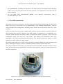
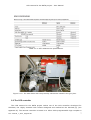
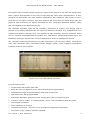
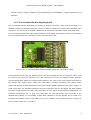
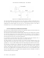
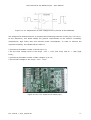
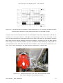
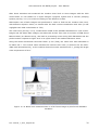
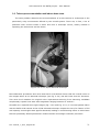
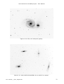
DIPARTIMENTO DI FISICA E ASTRONOMIA SEZIONE DI ASTRONOMIA CCD camera for the RATS project - User Manual - M. Focardi(a) (a) Dipartimento di Fisica e Astronomia – Università di Firenze, L.go E. Fermi 2, 50125 Firenze, Italy Technical Report TR01-2011 Version 1.0 First issue (v. 1.0): June 2010 Final release (v. 1.0): August 2011 Dipartimento di Fisica e Astronomia – Sezione di Astronomia L.go E. Fermi 2, 50125 Firenze (Italy) Ph.+39 (055) 205 5200 CCD camera for the RATS project – User Manual SUMMARY ABOUT THIS MANUAL ................................................................................................................... 4 1. THE RATS PROJECT ................................................................................................................. 5 2. CCD CAMERA MAIN FEATURES .......................................................................................... 5 2.1. The CCD camera head .......................................................................... 6 2.2. The CCD controller ............................................................................... 7 2.2.1 The Correlated Double Sampling board .................................................... 9 2.2.2 The Clock Driver and Bias Generator Board............................................. 10 2.2.3 The Sequencer board ........................................................................... 12 2.2.4 The NI Data Acquisition board............................................................... 14 2.3. 3. The high-level acquisition software ....................................................... 15 TESTS AND RESULTS ........................................................................................................... 17 3.1. Experimental set-up and laboratory tests............................................... 18 3.2. Telescope accommodation and indoor-dome tests ................................... 21 4. CONCLUSIONS ........................................................................................................................ 23 5. REFERENCES........................................................................................................................... 23 6. APPENDIX A – Boards Schematics ......................................................................................... 24 7. APPENDIX B – HiVeCam Brochure ........................................................................................ 24 8. APPENDIX C – Documentation CD ROM ............................................................................... 24 Ref.: Manual_1_2010_English.doc 2 CCD camera for the RATS project – User Manual Ref.: Manual_1_2010_English.doc 3 CCD camera for the RATS project – User Manual ABOUT THIS MANUAL This Manual reports on the CCD camera’s performance and characteristics developed at the XUVLab of the Department of Physics and Astronomy of the University of Florence, for the project RATS (RAdial velocity and Transit Search), that is an Italian-ESA collaboration, whose main goal is the search for extrasolar planets with the transit method. This Manual describes the characteristics of the CCD camera head and controller as well as the first tests at the Cima Ekar Schmidt telescope (Asiago, Italy). Keywords: CCD cameras, extrasolar planet, transit method. Ref.: Manual_1_2010_English.doc 4 CCD camera for the RATS project – User Manual 1. THE RATS PROJECT The RATS project is an Italian collaboration between several INAF Observatories (Padova, Catania, Napoli, Palermo), the Department of Physics and Astronomy of the University of Firenze, the Department of Physics and Astronomy of the University of Padua and ESA. The main goal of this project is the discovery of giant planets transiting solar type stars. The project will have a duration of some years during which the detection of at least ten new extrasolar planets is expected. The search for extrasolar planets is carried out through the transit photometric technique joined to a spectroscopic follow-up strategy for reconnaissance of false alarms. The main aim of the RATS project is twofold. The detection of extra solar planets that transit the disk of their parent star is the scientific driver of the whole project. In fact the Cima Ekar 67/92 Schmidt telescope, equipped with the present CCD camera, can observe simultaneously thousands of stars (magnitude range between 9th and 14th) in selected star fields. This method allows the discovery of new transiting planets. The second aim of the project is to use its observing strategy and the scientific data management as a bench work for a future space mission for planetary transit search. In order to achieve the RATS goals, two different telescopes are used for both the photometry search and the spectroscopic follow-up observations. The photometric transit search is performed at the Schmidt telescope, which mounts the CCD detector onto its folded focal plane. The spectroscopic follow-up observations are performed at the Copernico Telescope (182 cm Cassegrain Ritchey-Chretien) equipped with an echelle spectrograph. Planet candidate identification requires a preparatory work, starting from the stellar field selection with higher probability to find a transit event. An automatic photometric pipeline with a real-time image reduction will directly provide light curves of stellar objects in the field. The light curves will be analyzed in order to catch light dimming due to a transit. On a transit alarm, the candidate is observed with the spectroscopic telescope to rule out astrophysical false alarm like eclipse binary blended with giant stars. 2. CCD CAMERA MAIN FEATURES The camera is mainly composed by three parts: ü the CAMERA HEAD, including the dewar with the cold finger arrangements, the CCD sensor, the shutter and the detector proximity electronics (preamplifier, bias filters and waveshapers); Ref.: Manual_1_2010_English.doc 5 CCD camera for the RATS project – User Manual ü the CONTROLLER, including the sequencer, the ADC and the correlated double sampling (CDS) circuit, the clock driver and the bias generator, the temperature controller and the power supplies; ü the I/O AND DATA ACQUISITION BOARD, from National Instruments, that is accommodated into a PC. 2.1. The CCD camera head The RATS CCD camera is based on the SITe-424a back-illuminated 2048x2048 full-frame area device (see Fig.2.1.a and Tab.2.1.a for specifications). The SI-424a CCD imager is a silicon charge-coupled device designed to efficiently image scenes at low-light levels from UV to near infrared. CCD’s thinning and back-surface enhancement process provide superior quantum efficiency and increased blue and UV response. The CCD imager is configured in a windowless nonhermetic metal package and hosted inside an Oxford LN2 dewar, mounted on the CCD and preamplifier board (see Fig.2.1.b). Cold finger, wire cabling and mechanics have been fabricated at the Padua Astronomical Observatory. The window sealing the dewar is a field flattener lens with a 1500 mm focal length. The large area CCD cover a field of view of about 1 squared degree on the telescope focal plane, allowing the imaging of many candidate planetary systems around host stars. The camera head was mounted at the focal plane of the Cima Ekar Schmidt telescope where were performed focusing optimization procedures and scientific tests and measurements for the RATS objectives. Figure 2.1.a. SITe-424a CCD large area detector in its mounting brackets. Ref.: Manual_1_2010_English.doc 6 CCD camera for the RATS project – User Manual Table 2.1.a. SITe-424a device specifications. Figure 2.1.b. The LN2 dewar with the proximity electronics hosted in the grey box. 2.2. The CCD controller The CCD camera for the RATS project makes use of the CCD controller developed for HiVeCam, the Highly Versatile CCD Camera designed and realized at the XUVLab [6] (see Appendix B). The camera controller is based on a Xilinx CPLD programmable logic coupled to Ref.: Manual_1_2010_English.doc 7 CCD camera for the RATS project – User Manual the Hitachi microcontroller-based sequencer, whose main feature is the read-out speed lower than 1 Mpix/s that depends on the CCD current load and clock driver characteristics. In fact, owing to the SITe-424a very high clockline capacitance and resistance, was chosen to use a pixel rate of 115 kpx/s. However, this slow speed is still more than two times faster than the previous CCD controllers (50 kpx/s) developed for the “Telescopio Nazionale Galileo” (TNG) and early applied to the RATS project [8]. The HiVeCam controller hosts all the necessary electronics to acquire new images and to perform every action demanded by the high-level software interface. It is characterized by a modular architecture (see Fig.2.2.a). This provides a high versatility, as every electronic board can be removed and substituted for another one. This feature has several benefits since the laboratory prototype requires fine tuning of all boards in order to optimise the camera. The controller hosts several electronic circuits: Sequencer, A/D converter (ADC), Clock Driver (CD), Bias Generator (BG), Correlated Double Sampler (CDS), power supplies, temperature controller and I/O opto-couplers. Figure 2.2.a. The CCD camera controller. Its main features are: ü Continuously SW-tunable pixel rate ü Pixel rate up to 13 Mpixel/s (max. CPLD clocks frequency generation) ü Commands through serial link RS232; SCSI port for data I/O ü CCD timing fully SW programmable ü Automatic acquisition procedures with varying pixel rate and exposure time ü 9 clocks (-13V to +18V), 10 voltage biases (-3V to +33V) available to host any CCDs ü 16-bit signal resolution ü Time resolution up to 25 ns ü Temperature Control: -75°C to +10°C (Eurotherm temperature controller) ü Low power (5 W); battery operation optional Ref.: Manual_1_2010_English.doc 8 CCD camera for the RATS project – User Manual ü TCP/IP remote control, Sequencer programming and initialization, image acquisition and analysis. 2.2.1 The Correlated Double Sampling board The Correlated Double Sampling and analog-to-digital conversion (A/D) board is based on a classical clamp and sample electronic circuit in order to reduce the reset noise affecting each CCD pixel. The converter is a DATEL ADS932 with 16 bits of resolution, flash technology ADC. It is connected to the back plane board thanks to a 96-poles right-angle connector and located in the controller first box, starting from the left side front view. Figure 2.2.1.a. The Correlated Double Sampling and A/D conversion board. CCD sensors have a very low readout noise, thus any possible source of electronic noise must be reduced as much as possible. The A/D converter and the Correlated Double Sampler circuits significantly affect the camera performances: the noise level of the signal processing is the camera key quality factor. Great care was taken to design this board: the analog video signal was preserved and shielded by noisy sources like digital signals and PC power supply. In order to do that, the interface between the CCD Controller and the PC digital I/O was isolated via opto-couplers pairs. The same care was taken in the choice of the discrete components: all selected components are, in fact, very low-noise. As said previously, the converter is the ADS932 from DATEL: it is a reliable 16 bits ADC, capable to convert signals up to 2 MHz. The operational amplifier used in the CDS circuit is the AD8021 from Analog Devices, having an input voltage noise of 2.1 nV/Hz½. Ref.: Manual_1_2010_English.doc 9 CCD camera for the RATS project – User Manual Figure 2.2.1.b. CDS/ADC Board Schematic circuit. The reset noise affects each pixel-readout at the output stage by adding an offset bias level to the video signal. The CDS eliminates this noise by sampling twice the pixel video signal and subtracting the second sample from the first one. The functional scheme of the CDS is illustrated in Fig. 2.2.1.b, while the ADC-CDS PCB is shown in Fig. 2.2.1.a. 2.2.2 The Clock Driver and Bias Generator Board The Clock Driver and Bias Generator electronics are physically located on the same board; the first one on the top side, the latter on the bottom side. The clock driver circuit performs the following tasks: adjusts the clock voltage levels, performs the wave-form shaping and current driving operation. The generation of the bias voltages is one of the most delicate issues of a CCD camera, in fact they are directly fed, once filtered, to the CCD socket and from here to the sensor biasing pins. It is connected to the back plane board thanks to a 96-poles right-angle connector and is located in the controller second box, starting from the left side front view. The bias generation is a critical issue because it can directly introduce additional noise on the video signal. Since the intrinsic noise of the sensor is of the order of some µV peak-peak (typically 0.5 ÷ 5 µV), the bias voltages of the CCD output stage must introduce a lower noise. The CD plays an important role to determine the camera performances as well; the added noise, but mainly clock irregular waveforms, can affect the CCD charge transfer efficiency severely. The functional scheme of the CD is shown in Fig. 2.2.2.a. The main component of this circuit is the digital switch, the MAX333A from Maxim, since it is fully compatible to input logic TTL and CMOS levels, it is compact (each component hosts four switches), and fast (it has been tested to work up to 9 MHz). Ref.: Manual_1_2010_English.doc 10 CCD camera for the RATS project – User Manual Figure 2.2.2.a. Adjustment of clock voltage levels by means of the MAX333A. The designed CD and BG board is a compact PCB containing both the circuits (Fig. 2.2.2.b/.c). As the Sequencer, this board satisfy the general requirements of the camera: versatility, compactness, high frame rate and reduced power consumption. In order to achieve the required versatility, the CD/BG board is able to: • generate a selectable number of clocks up to 10; • set the clock voltage levels in the range –13V ÷ +1.3V (low level) and 0V ÷ +18V (high level); • generate a selectable number of bias voltages up to 12; • set the bias voltages in the range –14V ÷ +30V. Figure 2.2.2.b. The Clock Driver board (top). Ref.: Manual_1_2010_English.doc 11 CCD camera for the RATS project – User Manual Figure 2.2.2.c. The Bias Generator board (bottom). 2.2.3 The Sequencer board The Controller section dedicated to the generation of digital clocks for the readout of the CCD is generally called Sequencer, but also Logic Board or Timing Circuit. It provides digital clocks to the Clock Driver, but also the Clamp and Sample signals to the Correlated Double Sampling Circuit and the Start Convert to the A/D. It is connected to the back plane board thanks to a 96-poles right-angle connector and is located in the controller third box, starting from the left side front view. The Sequencer of the RATS Camera is based on 3 CPLD (Complex Programmable Logic Devices) from Xilinx and a Hitachi Microcontroller. In order to realize a versatile clocks generation a specific electrical schemes to be implemented in the CPLDs was designed. The on-chip implemented logic scheme (in schematic format) is based on a few logic components: counters, flip-flops and latches. The concept is very simple: each clock has two programmable counters, for the definition of the duration and of the time delay with respect to a reference clock. During the initialisation phase, the starting value for each counter is memorised by the respective latch; then, the latches load these values in the counters during the whole pattern generation. Setting a flip-flop pulls up a clock; at the same time the counter, which holds that clock time duration, starts counting. At the end of the counting, it resets the flip-flop and reloads its initial value. In Fig. 2.2.3.a an example of clock generation is shown just to illustrate the principle of operation. In particular the picture shows the clamp and sample generation scheme: dashed circles highlight the three logic levels (latch, counter, and flip-flop) and arrows indicate the two counters pulling the clamp signal up and down and therefore establishing the time delay and duration. Thus, all the clocks are tuneable: the initialisation of CPLD provides numbers to the counters and fixes the Ref.: Manual_1_2010_English.doc 12 CCD camera for the RATS project – User Manual duration of each clock and the delay of its rising edge with respect to a reference clock rising edge (in the example above the delay of the sample is referred to the clamp). Figure 2.2.3.a. Generation of the Clamp and Sample signals: the only purpose of this picture is to represent basic components levels (latches, counters, FFs) and the principle of operation. With similar logic schemes the horizontal and vertical clocks for a 3-clocks CCD are generated, the Reset signal and the Clamp, Sample and Start Convert control signals. Is it also possible to set the pixel rate and the number of rows and columns. The time resolution is a single clock period and therefore it depends on the selected oscillator. During the laboratory tests were acquired images at pixel rates ranging from 100 kHz up to 2 MHz and was used a 20 MHz system clock, so the time resolution was 50 ns. In Fig. 2.2.3.b the Sequencer printed circuit board (PCB) is shown; in this board is included three CPLDs, in order to keep sufficient resources for modifications and other possible requirements. Ref.: Manual_1_2010_English.doc 13 CCD camera for the RATS project – User Manual Figure 2.2.3.b. The Sequencer board based on 3 CPLD and a microcontroller. The Hitachi microcontroller is linked to the PC by means of a RS232 serial interface. Currently, the microcontroller is basically used to start-up CPLDs and to manage the CCD exposition and readout steps. The microcontroller is operated in a single-chip mode; in this mode the microcontroller uses only the internal ROM and RAM memory. This is particularly useful since the microcontroller does not need external devices to execute the program that is resident in the FLASH memory. A likely update concerning the microcontroller could be the implementation of other operations, such as temperature monitoring, movement of a telescope, grating, optics or filter wheel, coolant monitoring and refilling, triggering of the shutter, etc. After the sequencer box, starting from the left to the right, the controller hosts 3 power supplies modules and an Eurotherm module in order to monitor the temperature of a Peltierbased thermoelectric cooler (not in the case of RATS project were is used a dewar and a nitrogen-based cooling system). 2.2.4 The NI Data Acquisition board Currently, the data transfer from the Controller output to the PC is achieved via parallel readout; in fact it was selected a very fast DAQ (Data Acquisition) board, the NI6534 from National Instruments. National Instruments develop both hardware and software data acquisition tools: this ensures compatibility of issues, availability of drivers, correct interfacing and optimized performances. The NI6534 (see Fig. 2.2.4.a) has 32 Mbytes on-board memory and it achieves high-speed pattern I/O at rates up to 80 MB/sec. The NI6534 has 32 I/O bits and can be hosted in a desktop, in a embedded PC or in a laptop (via a dedicated adapter), in order to manage the data acquisition from two output amplifiers of a single CCD. Ref.: Manual_1_2010_English.doc 14 CCD camera for the RATS project – User Manual The DAQ board acquires the 16 parallel bits coming from the DATEL ADC through a SCSI connector positioned in the controller box rear panel. All the pixels are then displayed thanks to the IMAQ acquisition drivers and software provided by NI and integrated in the LabView high-level acquisition SW. Figure 2.2.4.a. The NI Data Acquisition board. 2.3. The high-level acquisition software The high-level SW interface (see Fig. 2.3.a/b/c/d) was developed under LabVIEW to provide users with very friendly operation procedures. The main features are: ü image displaying, processing and storage; ü automatic acquisition and displaying of the images; ü mathematical operation at single pixel level, including programmable binning; ü mathematical operation at image level; ü graphical tools; ü statistical image processing, including histogram and profile tools; ü a tool to pick-up part of the image for analysis, by means of a selection editor capable of unlimited shapes; ü export from proprietary format (.img) to standard formats (.bmp, .jpg, .tiff); ü image displayed in B/W or in false colours, by selecting among a varieties of palettes. Ref.: Manual_1_2010_English.doc 15 CCD camera for the RATS project – User Manual Figure 2.3.a. The high-level SW interface. The CCD camera is fully SW controllable for a quick setting of its main parameters. In fact, the user-friendly graphical interface allows for setting the best configuration of the selected CCD (format, timing, exposition time, pixel rate, vertical binning, etc.) and displaying on screen the waveforms of the clocks just set. Figure 2.3.b. The high-level SW interface with graphical clock timing capability. Ref.: Manual_1_2010_English.doc 16 CCD camera for the RATS project – User Manual In that way, inexpert users can easily configure the CCD parameters by comparing the obtained waveforms with those reported in the CCD datasheet. Moreover it is possible to remotely control every camera’s function, like setting the CCD parameters and sensor initialization, image acquisition and displaying. Figure 2.3.c. The histogram and profile graphical tools. Figure 2.3.d. The IMAQ area-selection tool. 3. TESTS AND RESULTS Some tests and instrumental set-ups were performed before delivery the CCD camera to the Asiago’s 67/92 Schmidt telescope. These tests aimed to get the following requirements: ü S/N P 400 @ mV = 14 (from Science requirements) ü At least 4-5 star magnitudes level in a image Ref.: Manual_1_2010_English.doc 17 CCD camera for the RATS project – User Manual ü Noise < 60 e- ü Versatility ü Remote controllable camera 3.1. Experimental set-up and laboratory tests Before CCD camera accommodation at the Cima Ekar Schmidt telescope, were performed some laboratory calibration activities in order to fully characterize the camera. Firstly, was operated a fine-tuning of all clocks and control signals (see Fig. 3.1.a and Fig. 3.1.b) to get a correct and “clean” (i.e. noise-free) video signal at the CCD output stage and were taken some preliminary images of a test target. Figure 3.1.a. An oscilloscope screenshot of horizontal phases H1, H2, H3 and reset signal. After fine-tuning of all clocks and control signals, the preamplifier gain and the post-amplifier gain stage on the CDS board were settled, in order to achieve the overall 16-bits full dynamic range of the AD converter, relating to the CCD output node responsivity. Ref.: Manual_1_2010_English.doc 18 CCD camera for the RATS project – User Manual Figure 3.1.b. An oscilloscope screenshot of vertical phases V1, V2, V3 during a vertical transfer between two consecutive lines readout performed on CCD shift register. The gain value on the CDS board and on the preamplifier board were respectively 1.54 and 57, providing so a conversion factor of 1.36 DN/e- (corresponding to a Gain of 0.74 e-/DN). In this way, the ADC saturation corresponded to about one third of the pixel full well capacity avoiding large field blooming effects affecting photometric measures. Combining in fact the ADC voltage input range (5.5 V) with its resolution (16 bit) we obtain an ADC sensitivity of 84 µV/DN. To get the readout chain Gain this value has to be divided by the output node responsivity (1.3 µV/e- in our case) multiplied by the total electronic stages gain (1.54x57=88). Figure 3.1.c. Experimental set-up: the dewar and preamplifier board with vacuum pipeline and cryogenic system. Ref.: Manual_1_2010_English.doc 19 CCD camera for the RATS project – User Manual After these activities was measured the readout noise level on some images with the CCD cooled down to 77K thanks to a liquid nitrogen cryogenic system and a vacuum pumping system (see Fig. 3.1.c) to avoid ice forming on the detector surface. Afterwards a set of dark images was performed in order to find-out the readout noise level, with different exposure times, to monitor also the dark current contribution with time (it was negligible with CCD cooled down to 77K). The noise level (see Fig. 3.1.d), measured as media of the standard deviations on a set of subimages and full-frame dark images, was about 45-50 DN. This noise is inclusive of FPN (Fixed Pattern Noise) on detector array, due both to processing errors during CCD fabrication and the pixels intrinsic response to light. So it is an upper limit to the readout electronic noise. Using the above-mentioned conversion factor (0.74 e-/DN), the noise level was estimated to be about 36 e-. This overall noise includes the intrinsic CCD noise (7 electrons for the SITe424a back-thinned device), so the readout electronics noise was below 35 e-, joining the target noise requirement of 60 e-. Figure. 3.1.d. Noise level measurements on a full-frame image as pixel levels standard deviation. Ref.: Manual_1_2010_English.doc 20 CCD camera for the RATS project – User Manual 3.2. Telescope accommodation and indoor-dome tests The main problem related to the accommodation of a CCD camera on a telescope is the particularly noisy environment offered by the overall system. There are, in fact, a lot of potential noise sources inside a dome and from a telescope mount, mainly related to operating the instrument and the dome. Figure 3.2.a. The 67/92 Schmidt telescope. Post-calibration procedures and noise tests have nevertheless shown that the overall noise on the images taken at the Schmidt telescope (see Fig. 3.2.a) was still lower than 40 electrons. This noise level matches the original noise requirements deriving from observing candidate exoplanetary system host stars with magnitude ranging between 9th and 14th. Hereafter are reported some light images (Fig. 3.2.b and Fig. 3.2.c) in inverted palette taken with the RATS CCD camera at the 67/92 Schmidt telescope. Despite the use of a fraction of full well capacity some bright stars appear saturated, leading to real blooming effect on CCD frame that can potentially affects photometric measurements and images reduction processes. Ref.: Manual_1_2010_English.doc 21 CCD camera for the RATS project – User Manual Figure 3.2.b. M51, the “Whirpool” galaxy. Figure 3.2.c. M65, M66 and NGC3628, the so called “Leo triplet”. Ref.: Manual_1_2010_English.doc 22 CCD camera for the RATS project – User Manual 4. CONCLUSIONS In this Manual are highlighted the main characteristics of the CCD camera for the RATS project developed at XUVLab of the Dept. of Physics and Astronomy of the University of Firenze. It has been shown that the main requirements on the signal to noise ratio for the search for extrasolar planets with the transit method in the RATS project contest has been achieved. Moreover this document reports some astronomical images taken with the CCD camera mounted at the C.ma Ekar 67/92 Schmidt telescope to show their qualities. Finally, Appendix A reports on Boards Schematics, Appendix B on the HiVeCam CCD Camera brochure as initially developed in 2007 and Appendix C contains a CD ROM with the camera’s full documentation. 5. REFERENCES [1] A. Gherardi, E. Pace, L. Gori, M. Focardi, M. Sozzi, G. Rossi, F. Tosetti. “CCD camera for space-based solar corona observation” Proceeding Frontier Science, 2004. http://www.roma2.infn.it/iwfs04/iwfs.html [2] A. Gherardi, L. Gori, M. Focardi, E. Pace, M. Romoli, S. Fineschi, L. Zangrilli, D. Gardiol, E. Antonucci. "CCD camera for ground and space-based solar corona observations" SPIE Proceedings: Telescopes and Instrumentation for Solar Astrophysics, Vol. 5171, pp. 247-257, 2004. http://adsabs.harvard.edu/abs/2004SPIE.5171..247G [3] L. Gori. “CCD camera for the polarimetric channels of HERSCHEL” – Ph.D. Thesis a.a. 2002-2003, Dep. of Astronomy and Space Science, Florence University. [4] A. Gherardi. “Elettronica di controllo per la camera CCD del canale polarimetrico di HERSCHEL” Degree Thesis a.a. 2001-2002, Dep. of Astronomy and Space Science, Florence University. [5] R. Claudi, S. Scuderi, P. Bruno, L. Contri, A. Gherardi, V. Granata, M. Focardi, E. Pace. “Radial Velocity and Transit Search (RATS) II” Poster session - Jenam 2008, Vienna. [6] E. Pace, L. Gori, A. Gherardi, M. Focardi. “HiVeCam brochure” http://www.astro.unifi.it/~xuvlab/website/docs/brochure_hivecam.pdf [7] RATS project – Home page http://www.pd.astro.it/rats/en/home.php [8] S. Scuderi, R.U. Claudi, F. Favata, G. Bonanno, P. Bruno et al. “The CCD cameras of RATS project” Mem. S.A.It. Suppl. Vol. 9, 478 - SAIt 2006 http://sait.oat.ts.astro.it/MSAIS/9/PDF/478.pdf Ref.: Manual_1_2010_English.doc 23 CCD camera for the RATS project – User Manual 6. APPENDIX A – Boards Schematics In the Appendix A of this Manual are reported all the camera’s electronics boards schematics as itemized below: ü Preamplifier board schematic; ü CDS/ADC board schematic; ü CD and BG board schematic; ü Sequencer board schematic; ü Controller BUS board schematic, ü Power Supplies BUS board schematics. 7. APPENDIX B – HiVeCam Brochure In the Appendix B of this Manual is reported the early 2007 HiVeCam Brochure, the Higly Versatile CCD camera entirely developed at the XUVLab of the Dep. of Astronomy and Space Science of the University of Firenze, whose controller is the same of that used for the RATS project. In fact we replaced only the compact HiVeCam camera head with the larger Oxford LN2 dewar in order to host and to cool-down the SITE 424-a CCD large-area array detector with liquid nitrogen. From the data reported in the brochure is it possible to have a detailed overview of the controller main characteristics. 8. APPENDIX C – Documentation CD ROM In the Appendix C of this Manual is reported the complete documentation related to the present CCD camera. The CD ROM contains all the boards electronics schematics and layouts, datasheets, boards photos, notes, software, etc. Ref.: Manual_1_2010_English.doc 24 Dip. di Astronomia e Scienza dello Spazio Università di Firenze A Finmeccanica Company Highly Versatile CCD Camera The Ultimate Solution Dip. di Astronomia e Scienza dello Spazio Università di Firenze A Finmeccanica Company APPLICATION MARKETS • Imaging & Spectroscopy • Life Science (microscopy, general analysis, fluorescence) • High performance Imaging Market (e.g. bio-technology, X-ray, Astronomy) WITH POSSIBLE USE AS • Laboratory multifunctional CCD Camera • Slow-scan or high frame rate spectroscopy and high-resolution imaging • Wide field imaging • Fine guidance systems ADVANTAGES FROM USING THE High modularity: users achieve different camera applications by changing simply the CCD sensor or adding or removing electronic boards Upgradeable: expand or renew the Camera by adding new boards or substituting the old one High performance (low noise, high dynamic range, slow scan or high frame rate) Continuously tunable pixel rate TCP/IP based remote testing, programming, diagnostics, and image acquisition User friendly Camera Programming and Image Acquisition & Processing, based on LabVIEW® Compact and low power instrument, portable version with air- or fluid-cooled, Peltier available. Dip. di Astronomia e Scienza dello Spazio Università di Firenze A Finmeccanica Company DESCRIPTION OF THE CAMERA Camera head Controller The Camera is composed by three parts: CAMERA HEAD, including the objective, the CCD sensor, the Peltier cooling Sequencer stage (if required), the detector proximity electronics; CONTROLLER, including the Sequencer, the ADC and the Correlated Double Sampling Circuit, the Clock Driver and the Bias Generator, the Temperature CCD Bias generator Peltier Power CDS Supply ADC 16 bit ACQUISITION BOARD from National Instruments® to be put in a PC. Control & Acquisition Board Sequencer RS232 CDS + 16 bit ADC Start -up; Controls PC NI Acquisition Board Clock driver + Bias generator Clocks Clocks ; Biases Image SCSI Video Signal CCD Filters Proxy ..... Controller; Clock driver (Remote PC) Dip. di Astronomia e Scienza dello Spazio Università di Firenze A Finmeccanica Company TECHNICAL DETAILS Cooling system Vacuum I/O CAMERA HEAD Main features: Support CCD formats up to 4096×4096 pixel Up to 4 readout ports CCD Peltier Modules Quartz window, windowless or C-type objective Schematic view of the camera head Low noise proxy electronics (1.8 nV/√Hz rms) Minimum cooling temperature: -75°C (Peltier) The camera head and the close-cycle fluid circuit PT100 temperature sensor in the cold finger Air- or fluid-cooled Peltier with closed-cycle fluid circulation available Very compact design (∅ 9 cm, L 12.5 cm) Lightweight (1.5 kg) High vacuum compatible (10-7 mbar) The Camera Head Dip. di Astronomia e Scienza dello Spazio Università di Firenze A Finmeccanica Company CONTROLLER Main features: Continuously SW tunable pixel rate Pixel rate up to 13 Mpixel/s Commands through serial link RS232; SCSI port for data I/O Any CCD timing fully SW programmable Automatic acquisition procedures with varying pixel rate and exposure time 9 clocks (-13V to + 18V), 10 bias (-3V to +33V) available to allow easy interface with any CCD Dynamic range: 16 bit @ 2 Msample/s Time resolution up to 25 ns Temperature Control: -75°C to +10°C The Controller Low power (5 W); battery operation optional TCP/IP remote control, Sequencer programming and initialization, image acquisition and analysis Remote debugging and testing available External peripherals (motors, shutters, ancillary sensors etc.) can be connected and controlled Portable version available with lap-top connections, battery power supply and closed-cycle fluid circulation included Dip. di Astronomia e Scienza dello Spazio Università di Firenze A Finmeccanica Company SW FOR CAMERA CONTROL Fully SW controllable Camera (LabVIEW® platform) for a quick setting of parameters. A User friendly graphical interface allows: Setting configuration for the selected CCD (format, timing, exposition time, pixel rate, vertical binning, etc.); To remotely control every function of the camera: we can configure the CCD parameters and initialize the sensor, acquire and display the resulting image. Moreover, it is possible to perform remote diagnostics tools and to upgrade resident programs Displaying on screen the waveforms of the clocks just set: novice users can easy configure the CCD parameters by comparing the obtained waveforms with those reported in the CCD datasheet Dip. di Astronomia e Scienza dello Spazio Università di Firenze A Finmeccanica Company SW FOR IMAGE ACQUISITION AND ANALYSIS The SW interface has been developed under LabVIEW® to provide Users with very friendly operation. The main features are: image display, processing and storage; automatic acquisition and display of following images; mathematical operation at single pixel level, including programmable binning; mathematical operation at image level; graphical tools; statistical image processing, including Histogram and Profile tools; a tool to pick a part of the image up to be analysed, by means of a selection editor capable of unlimited shapes; export on standard formats (FITS optional); image displayed in B/W or in false colours, selecting between a varieties of palettes. Dip. di Astronomia e Scienza dello Spazio Università di Firenze A Finmeccanica Company SPECIFICATIONS Array size Linear or array CCD up to 4096×4096 pixels Wavelength range NIR, VIS, UV, soft-X ray, X-ray PC interface RS232 Serial interface and 68 pins National Instruments cable to NI6533 acquisition board Software interface LabVIEW6i based proprietary interface OS platform Windows®, Unix®, Linux®, MacOS® Digital resolution 16 bit @ 2MHz Readout noise 25 electrons Pixel Binning Programmable Exposure time Config. “Normal”: 1 ms to 17 min (1 ms step); CCD Timing Software selectable up to 4 parallel and serial clocks Cooling system 3-stage Peltier TEC with external fluid-cooled heat sink. Minimum temperature: –75° C ( @ 2 × 10⁻⁶ mbar) Camera head Modular aluminium body; ∅ 9 cm, L 12.5 cm, 1.5 kg weight. C mount or equivalent. HV compatible down to 10-7 mbar Max. power consumption 5 W without TEC; 33 W with a 3-stage TEC Temperature control External digital thermostat controller with 0.1°C fine regulation Weight 1.5 kg Camera Head; ~ 7.5 kg total weight (camera head + controller + external liquid heat exchanger) Config. “Astronomy”: 1 s to hours (1 s step) Dip. di Astronomia e Scienza dello Spazio Università di Firenze A Finmeccanica Company APPLICATIONS VACUUM UV Use of UV-enhanced thinned back-side illuminated CCD Wavelength range: 30 ÷ 200 nm Quantum efficiency: 20% @ 100 nm, 60% @30 nm (quantum yield not included) Possibility of low energy-resolution photon counting @ 30 nm High vacuum compatible camera Windowless operation Min. cooling temperature: -75°C Possibility of thermal cycles Remote cooling option available Improved stability of the quantum efficiency Applications to astronomy, lasers, photolithography, microscopy, spectroscopy, atomic and molecular physics and chemistry, fluorescence, plasma physics, FUV and EUV imaging VUV high-order laser harmonic generation X RAYS Use of fully depleted CCDs Use of front side illuminated CCD coupled to phosphors (P45 et al.) Wavelength range 40 eV ÷ 10 KeV Quantum efficiency: > 60% Photon counting operation available Energy resolution UHV compatible camera Windowless or tapered (1:3 or 1:4) operation Remote cooling option available Min. cooling temperature: -75°C Applications to astronomy, spectroscopy, microscopy, synchrotron radiation, surface analysis, fluorescence, plasma physics, medical applications, X-ray imaging Thermal link Peltier CCD Remote cooling concept Dip. di Astronomia e Scienza dello Spazio Università di Firenze A Finmeccanica Company is a product that results from the collaboration between the XUVLab of the Department of Astronomy and Space Science at the University of Florence and the Galileo Avionica Contacts: Dott. Emanuele Pace ([email protected]) Dott. Alessandro Gherardi ([email protected]) Dott. Mauro Focardi ([email protected]) Dipartimento di Astronomia e Scienza dello Spazio Largo E. Fermi 2, 50125 Firenze - Italia http://www.arcetri.astro.it/Dipartimento/xuvlab/