1
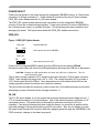
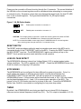
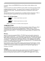
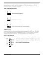
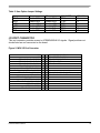
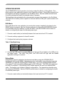
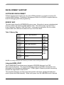
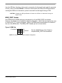
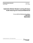
Freescale Semiconductor
User Guide
DEMO9S08QG8UG
Rev. 0, 12/2006
Application Module Student Learning Kit Users
Guide featuring the Freescale MC9S08QG8
For use with the following part numbers:
APS08QG8SLK
PBS08QG8SLK
CSM9S08QG8SLK
DEMO9S08QG8SLK
© Freescale Semiconductor, Inc., 2006. All rights reserved.
_______________________________________________________________________
CONTENTS
CAUTIONARY NOTES ...........................................................................................................................4
TERMINOLOGY ......................................................................................................................................4
FEATURES ................................................................................................................................................5
REFERENCES...........................................................................................................................................6
INTRODUCTION......................................................................................................................................7
GETTING STARTED ...............................................................................................................................7
POWER .................................................................................................................................................. 7
POWER SELECT............................................................................................................................... 8
PWR_SEL........................................................................................................................................... 8
VX_EN ............................................................................................................................................... 8
RESET SWITCH ................................................................................................................................... 9
LOW VOLTAGE DETECT................................................................................................................... 9
STOP MODES ....................................................................................................................................... 9
TIMING.................................................................................................................................................. 9
COMMUNICATIONS......................................................................................................................... 10
SCI PORT ........................................................................................................................................ 10
COM_EN ......................................................................................................................................... 10
COM CONNECTOR ........................................................................................................................ 11
SPI PORT......................................................................................................................................... 12
IIC PORT ......................................................................................................................................... 12
USER OPTIONS.................................................................................................................................. 12
PUSHBUTTON SWITCHES ............................................................................................................ 12
LED INDICATORS .......................................................................................................................... 12
POTENTIOMETER ......................................................................................................................... 12
PHOTOCELL................................................................................................................................... 12
I/O PORT CONNECTOR .................................................................................................................... 13
OPERATING MODES ........................................................................................................................ 14
RUN MODE..................................................................................................................................... 14
DEBUG MODE ............................................................................................................................... 14
DEVELOPMENT SUPPORT ................................................................................................................16
SOFTWARE DEVELOPMENT.......................................................................................................... 16
MEMORY MAP................................................................................................................................ 16
INTEGRATED BDM_PORT .............................................................................................................. 16
BDM_PORT HEADER ....................................................................................................................... 17
2
Freescale Semiconductor
FIGURES
Figure 1: PWR_SEL Option Header ......................................................................................................8
Figure 2. VX_EN Option Header ...........................................................................................................9
Figure 3: OSC_EN Option Header .......................................................................................................10
Figure 4: COM Connector......................................................................................................................11
Figure 5: MCU I/O Port Connector .......................................................................................................13
Figure 6: BDM Port .................................................................................................................................17
TABLES
Table 1: COM_EN Option Header........................................................................................................11
Table 2: User Option Jumper Settings.................................................................................................13
Table 3: Run Mode Setup ......................................................................................................................14
Table 4: Debug Mode Setup .................................................................................................................15
Table 5: Memory Map.............................................................................................................................16
REVISION
Date
December 14, 2005
Freescale Semiconductor
Rev
0
Comments
Initial Release.
3
CAUTIONARY NOTES
♦ Electrostatic Discharge (ESD) prevention measures should be used when handling this
product. ESD damage is not a warranty repair item.
♦ Axiom Manufacturing does not assume any liability arising out of the application or use of
any product or circuit described herein; neither does it convey any license under patent
rights or the rights of others.
♦ EMC Information on the APS08QG8SLK board:
a) This product, as shipped from the factory with associated power supplies and cables,
has been verified to meet with FCC requirements as a CLASS A product.
b) This product is designed and intended for use as a development platform for hardware
or software in an educational or professional laboratory.
c) In a domestic environment, this product may cause radio interference in which case the
user may be required to take adequate prevention measures.
d) Attaching additional wiring to this product or modifying the product operation from the
factory configuration may affect its performance and cause interference with other
apparatus in the immediate vicinity. If such interference is detected, suitable mitigating
measures should be taken.
TERMINOLOGY
This development board uses option selection jumpers. A jumper is a plastic shunt that
connects 2 terminals electrically. Terminology for application of the option jumpers is as
follows:
Jumper – a plastic shunt that connects 2 terminals electrically
Jumper on, in, or installed - jumper is installed such that 2 pins are connected together
Jumper off, out, or idle - jumper is installed on 1 pin only. It is recommended that
jumpers be idled by installing on 1 pin so they will not be lost.
Cut-Trace – a circuit trace connection between component pads. The circuit trace may
be cut using a razor knife to break the default connection. To reconnect the circuit,
simply install a suitably sized 0-ohm resistor or attach a wire across the pads.
Throughout this document, where used, the name APS08QG8SLK applies equally to the
APS08QG8SLK, CSM9S08QG8SLK, and PBS08QG8SLK.
4
Freescale Semiconductor
FEATURES
The APS08QG8SLK is an educational application module for the Freescale Semiconductor
MC9S08QG8 microcontroller. Development of applications is quick and easy with the
integrated USB-BDM, sample software tools, and examples. An optional BDM_PORT port is
also provided to allow use of a BDM_PORT cable. A 32-pin connector allows connecting the
APS08QG8SLK board to an expanded evaluation environment.
•
•
•
•
•
•
•
•
•
•
MC9S08QG8 CPU, 16-pin DIP, Socketed
• 8K Byte Flash
• 512 Bytes RAM
• Internal 32 kHz Oscillator, trimmable to ±0.2%
• 12 GPIO, 1 Input Only, 1 Output only
• Timer Interface Module
• SCI and SPI Communication Ports
• IIC Module
• 8 KBI inputs
• 2-Ch, 16-bit, Timer Interface
• 8-Ch, 10-bit Analog to Digital Converter (ATD)
• Analog Comparator w/ internal compare
Integrated USB-BDM
RS-232 Serial Port w/ DB9 Connector
SPI, IIC ports available on Connector J1
External 32.768 kHz Clock Oscillator (not
installed)
Power Input Selection Jumper
• Power input from USB-BDM
• Power input from on-board regulator
• Power input from Connector J1
• Power output through Connector J1
User Components Provided
• 3 Push Switches; 2 User, 1 Reset
• 3 LED Indicators; 2 User, 1 VDD
Jumpers
• USER_EN
• PWR_SEL
• COM_SEL
• VX_EN
• OSC_EN (not installed)
Connectors
• 32-pin MCU I/O Connector
• 2.0mm Barrel Connector
• BDM_PORT Pin Header (not installed)
• DB9 Serial Connector
Specifications:
• Board Size 2.9” x 2.5”
• Power Input:
• USB Cable – 500mA max
•
PWR Connector - 9VDC typical, +7VDC to +18VDC
Freescale Semiconductor
5
REFERENCES
Reference documents are provided on the support CD in Acrobat Reader format. More
information can be found in the Application Notes section of the Freescale Web site.
APS08QG8SLKUG.pdf
HCS08QG8SCHEMSLKREVC.pdf
DEMO9S08QG8QSG.pdf
DEMO9S08QG8TEST.zip
DEMO9S08QG8_APP.pdf
DEMO9S08QG8APP.zip
AN2627.pdf
APS08QG8SLK User Guide (this document)
APS08QG8SLK Board Schematic, Rev. C
Quick Start Guide for Demonstration application
CodeWarrior demonstration application software
Test Application User Guide
CodeWarrior LED demonstration application software
Cycle-by-Cycle Instruction Details for HC(S)08 MCU’s
Visit www.freescale.com\universityprogram for current product information, reference materials
and updates.
6
Freescale Semiconductor
INTRODUCTION
Before using this module, the user should be familiar with the hardware and software operation
of the target MCU. Refer to the MC9S08QG8 User Manual and MC9S08QG8 Reference
Manual for details on MCU operation. The module’s purpose is to promote the features of the
MC9S08QG8 and to assist the user in quickly developing an application in a known working
environment. Users should be familiar with memory mapping, memory types, and embedded
software design for quick, successful, application development.
The APS08QG8SLK application module is a fully assembled, fully functional module
supporting Freescale MC9S08QG8 microcontroller for educational use. The module comes
with a integrated USB Background Debug Mode (BDM), and USB cable for stand-alone
operation. Support software for this module is provided for Windows 95/98/NT/2000/XP
operating systems.
GETTING STARTED
To get started quickly, please refer to the DEMO9S08QG8 Quick Start Guide included with the
development kit. This quick start shows how to connect the board to the PC, run an LED test
program, install the correct version of CodeWarrior Development Studio, and load an Analog to
Digital (ATD) test program using CodeWarrior.
OPERATION
POWER
The APS08QG8SLK is designed to be powered from the USB_BDM during application
development. A 2.0mm barrel connector has been applied to support stand-alone operation.
In addition, the board may be powered through connector J1. The board may also be
configured to supply power through connector J1 to external circuitry.
When using the integrated USB-BDM, the board draws power from the USB bus. Total
current consumption of the board and connected circuitry, therefore, must be limited to less
than 500mA. Excessive current drain will violate the USB specification causing the USB bus
to disconnect. This will force a power-on-reset (POR).
CAUTION: Violating the USB specification will cause the USB bus to disconnect, forcing the
target to reset.
A 2.0mm barrel connector input has been provided to allow stand-alone operation. Voltage
input at this connector must be limited to between +5V and +18V. An LDO voltage regulator at
VR1 converts the input voltage to the +3.3V rail on the target board. VR1 will shut down if the
connected circuit draws excessive current. Stand-alone operation is also supported through
connector J1.
Freescale Semiconductor
7
POWER SELECT
Power may be applied to the board through the integrated USB-BDM circuitry, a 2.0mm barrel
connector, or through connector J1. Power selection is achieved by using 2 option headers:
PWR_SEL option header and the VX_EN option header.
The PWR_SEL option header selects power input either from the integrated USB-BDM
circuitry or from the on-board voltage regulator. Power input selection, from the USB-BDM or
the on-board power supply, is mutually exclusive. This prevents power-input contention from
damaging the board. The figure below details the PWR_SEL header connections.
PWR_SEL
Figure 1: PWR_SEL Option Header
PWR_SEL
VB
▪
▪
VDD
▪
CONFIGURATION:
Select power input from USB-BDM
PWR_SEL
VB
▪
▪
VDD
▪
Select power input from VR1
Power from the integrated BDM is drawn from the USB bus and is limited to 500mA.
Excessive current drain will violate the USB specification will cause the USB bus to disconnect.
CAUTION: Violating the USB specification will cause the USB bus to disconnect. This will
cause the board to reset.
The on-board voltage regulator (VR1) accepts power input through a 2.0mm barrel connector
(PWR). Input voltage may range from +5V to +18V. The voltage regulator (VR1) provides a
+3.3V fixed output limited to 250mA. Over-temperature and over-current limits built into the
voltage regulator protects the device from excessive stresses.
The user should consider the maximum output current limit of the selected power source when
attempting to power off-board circuitry through connector J1.
VX_EN
The VX_EN option header is a 2-pin jumper that connects the target board voltage rail to J1-1.
J1-3 is connected directly to the ground plane. Use of this feature requires a regulated +3.3V
input power source. This power input is decoupled to minimize noise input but is not
regulated. Care should be exercised when using this feature; no protection is applied on this
input and damage to the target board may result if over-driven. Also, do not attempt to power
the target board through this connector while also applying power through the USB-BDM or the
PWR connector; damage to the board may result.
8
Freescale Semiconductor
Power may be sourced to off-board circuitry through the J1 connector. The current limitation of
the USB bus or the on-board regulator must be considered when attempting to source power
to external circuitry. Excessive current drain may damage the target board, the host PC USB
hub, or the on-board regulator. The figure below details the VX_EN option header
connections.
Figure 2. VX_EN Option Header
ON
Enable power connection to connector J1
OFF
Disable power connection to connector J1
VX_EN
▪
▪
VX_EN
CAUTION: Do not apply power to connector J1 while also sourcing power from either the PWR
connector or the USB-BDM circuit. Damage to the board may result.
NOTE: Do not exceed available current supply from the USB-BDM cable or on-board regulator
when sourcing power through connector J1 to external circuitry.
RESET SWITCH
The RESET switch provides a method to apply an asynchronous reset to the MCU and is
connected directly to the PTA5/RESET* input on the MCU. Pressing the RESET switch forces
the MCU RESET* input low. The MC9S08QG8 MCU applies an internal pull-up on the
RESET* line to prevent spurious resets and allow normal operation.
LOW VOLTAGE DETECT
The MC9S08QG8 utilizes an internal Low Voltage Detect (LVD) to protect against undervoltage conditions. The LVD is enabled out of RESET. Consult the MC9S08QG8 Device User
Guide for details on configuring LVD operation.
STOP MODES
The MC9S08QG8 can be configured for three different low power stop modes. If stop1 or
stop2 modes are entered, an external pull-up resistor must be placed between the
PTA5/RESET*/IRQ*/TCLK pin and VDD. This pull-up resistor is not included on the
APS08QG8SLK board. If these modes will be used with this board, a 10K – 50K ohm resistor
can be placed between pins J1-1 and J1-2 to ensure proper operation of the MCU. The
jumper for the VX_EN header must also be in place in this case. Consult the MC9S08QG8
Device User Guide for more details on configuring the low power stop modes.
TIMING
By default, the APS08QG8SLK uses timing provided from an internal 32 kHz frequency
reference and an internal frequency-locked loop (FLL). The FLL output is trimmable to ± 0.2%
Freescale Semiconductor
9
of nominal. Refer to the MC9S08QG8 Device User Guide for further details on clock
operation.
Component pads for an optional 32.768 kHz crystal oscillator circuit have also been provided
to support external timing input. The external crystal is connected to the PTB6/XTAL and
PTB7/EXTAL MCU inputs. This alternate timing source is configured for Pierce mode
operation.
The alternate timing source components are not installed in default configurations. Refer to
the board schematic to populate this option and associated support components.
Figure 3: OSC_EN Option Header
▪
▪
ON
Enables Crystal Oscillator Input to MCU
OFF
Disables Crystal Oscillator Input to MCU
OSC_EN
▪
▪
OSC_EN
NOTE: This option header is not installed in default configuration.
COMMUNICATIONS
The APS08QG8SLK board provides a Serial Communications Interface (SCI) port, a Serial
Peripheral Interface (SPI) port, and an Inter-Integrated Controller (IIC) port. RS-232
communications are supported through a DB9 connector. SPI and IIC communications are
supported through connector J1. The COM_EN option header enables SCI operation on the
board.
SCI Port
An RS-232 transceiver provides RS-232 to TTL/CMOS logic level translation between the
COM connector and the MCU. The COM connector is a 9-pin Dsub, right-angle connector. A
ferrite bead on shield ground provides conducted immunity protection. Communication signals
TXD and RXD are routed from the transceiver to the MCU. These signals are also available
on connector J1. Hardware flow control signals RTS and CTS are available on the logic side
of U3 and are routed to test point vias located near the transceiver (U4). RTS has been biased
properly to provide handshaking if required.
Communications signals TXD and RXD connect to general purpose Port B signals. The RS232 transceiver should be disabled via the COM_EN option header if these signals are used
as GPIO. The transceiver should also be disabled if the TXD and RXD signal inputs at
connector J1 are used.
COM_EN
The COM_EN option header determines the operational status of the RS-232 transceiver. In
the OFF position, the transceiver is disabled and all outputs are tri-stated. In the PTA4
position, the transceiver may be turned on or off using MCU GPIO signal PTA4. With the
10
Freescale Semiconductor
option jumper removed, the transceiver is always on. When the transceiver is ON, the
AutoShutoff feature of the device is disabled.
Table 1: COM_EN Option Header
PTA4
OFF
▪
▪
▪
MCU controls RS-232 Transceiver
COM_EN
PTA4
OFF
▪
▪
▪
RS-232 Transceiver disabled
COM_EN
PTA4
OFF
▪
▪
▪
RS-232 Transceiver always ON. AutoShutoff disabled
COM_EN
COM Connector
A standard 9-pin Dsub connector provides external connections for the SCI port. The Dsub
shell is connected to board ground through a ferrite bead. The ferrite bead provides noise
isolation on the RS-232 connection. The DB9 connector pin-out is shown below.
Figure 4: COM Connector
4, 6
1
TXD
2
RXD
3
1, 6
4
GND
5
6
1, 4
7
RTS
Female DB9 connector that interfaces to the HC(S)08 internal SCI1 serial
port via the U2 RS232 transceiver.
It provides simple 2-wire
asynchronous serial communications without flow control. Flow control is
provided at test points on the board.
8
CTS
Pins 1, 4, and 6 are connected together.
9
NC
Freescale Semiconductor
11
SPI Port
SPI signaling connects directly between connector J1 and the MCU. Refer to the
MC9S08QG8 Device User Guide for details on using the SPI interface.
IIC Port
IIC signaling connects directly between connector J1 and the MCU. Refer to the MC9S08QG8
Device User Guide for details on using the IIC interface.
USER OPTIONS
The APS08QG8SLK includes various input and output devices to aid application development.
User I/O devices include 2 momentary pushbutton switches, 2 green LEDs, 1 potentiometer,
and 1 phototransistor. Each device may be enabled or disabled individually by the USER_EN
option header. Each user enable is clearly marked as to functionality.
Pushbutton Switches
Two push button switches provide momentary, active-low input, for user applications. Pull-ups
internal to the MCU must be enabled to provide error free switch operation. Pushbutton
switches SW1 and SW2 are enabled to the MCU I/O ports by the USER option bank. SW1
and SW2 connect to input ports PTA2 and PTA3 respectively. Table 2 below details the user
jumper settings.
LED Indicators
Indicators LED1 and LED2 are enabled from HC(S)08 I/O ports by the USER option bank.
Each LED is active-low and illuminates when a logic low signal is driven from the respective
MCU I/O port. MCU ports PTB6 and PTB7 drive LED1 and LED2 respectively. Table 2 below
details the user jumper settings.
Potentiometer
A 5k ohm, thumb-wheel type, potentiometer at RV1 provides variable resistance input for user
applications. The output is the result of a voltage divider that changes as the thumb-wheel is
turned. The potentiometer is connected between VDD and GND with the center tap providing
the divider output. This center tap is connected to the MCU on signal PTA0. Table 2 below
details the user jumper settings.
Photocell
A surface-mount phototransistor provides light sensitive, variable input for user applications.
Current flow within the phototransistor is inversely proportional to light intensity incident on the
surface of the device. A rail-to-rail OP amp at U2 boosts the photocell output to useable
levels. This signal is available to the MCU on signal PTA1. Table 2 below details the user
jumper settings.
12
Freescale Semiconductor
Table 2: User Option Jumper Settings
Jumper
SW1
SW2
LED1
LED2
RV1
RZ1
On
Enable SW1
Enable SW2
Enable LED1
Enable LED2
Enable RV1
Enable RZ1
Off
Disable SW1
Disable SW2
Disable LED1
Disable LED2
Disable RV1
Disable RZ1
MCU PORT
PTA2
PTA3
PTB6
PTB7
PTA0
PTA1
MCU PIN
14
13
6
5
16
15
I/O PORT CONNECTOR
This port connector provides access to APS08QG8SLK I/O signals. Signal positions not
shown listed are not connected on the board.
Figure 5: MCU I/O Port Connector
VDD
VSS
PTB1/KBI1P5/ADC1P5/TXD1
PTB0/KBI1P4/ADC1P4/RXD1
PTA2/KBI1P2/ADC1P2/SDA1
PTA3/KBI1P3/ADC1P3/SCL1
PTA5/ RESET*/IRQ*/TCLK
PTA0/KBI1P0/ADC1P0/TPM1CH0/AMCP+
PTB3/KBI1P7/ADC1P7/MOSI1
PTB4/MISO1
PTB2/KBI1P6/ADC1P6/SPSCK1
PTB5/TPM1CH1/SS1
PTA1/KBI1P1/ADC1P1/ACMP1PTB6/SDA1/XTAL
PTB7/SCL1/EXTAL
PTA4/BKGD/MS/ACMP10
Freescale Semiconductor
1
3
5
7
9
11
13
15
17
19
21
23
25
27
29
31
2
4
6
8
10
12
14
16
18
20
22
24
26
28
30
32
PTA5/RESET*/IRQ*/TCLK
PTA5/ RESET*/IRQ*/TCLK
PTA4/BKGD/MS/ACMP10
PTB7/SCL1/EXTAL
PTB6/SDA1/XTAL
PTA1/KBI1P1/ADC1P1/ACMP1PTA0/KBI1P0/ADC1P0/TPM1CH0/AMCP+
13
OPERATING MODES
The APS08QG8SLK board operates in two basic modes Run Mode, or Debug Mode. Run
Mode supports user application operation from Power-On or Reset. Debug Mode supports the
development and debug of applications via the BDM_PORT. See the related sections below
for quickly starting the board in the desired mode of operation.
The board has been preloaded with a demonstration program that operates in the Run Mode.
The VDD LED is lit when power is applied to the board and the PWR_SEL option header is set
correctly.
RUN Mode
Run mode allows the user application to execute when power is applied to the board or the
RESET button is pressed. Use the following settings to configure the APS08QG8SLK board
for RUN Mode using the USB bus to power the board. See the POWER section below for
details on configuring the board for alternate power input.
1. Connect a serial cable (not included) between the board and a host PC if needed.
2. Connect auxiliary equipment to board if needed.
3. Configure the board option jumpers as shown.
Table 3: Run Mode Setup
PWR_SEL
COM_EN
VX_EN
USER_EN
Set to VB
Set to PTA4
ON if required
ALL ON
4. Connect the USB cable to an open USB port on the host PC and attach to the USB port on
the target board. The USB, USB_PWR, and VDD LEDs will light and the loaded
application will begin to execute.
Debug Mode
Debug Mode supports application development and debug using the HCS08/HC(S)12
background debug mode (BDM). Background mode is accessible using either the integrated
USB-BDM or an external HCS08/HC(S)12 BDM cable. Use of the integrated BDM requires
only a host PC with an available USB port and an A/B USB cable. The USB cable used must
be USB 2.0 compliant. A 6-pin BDM_PORT header supports the use of an external BDM
cable. This header is not installed in default configurations. The steps below describe using
the integrated USB-BDM. See the POWER section below for details on configuring the board
for alternate power input.
1. Connect a serial cable (not included) between the board and a host PC if needed.
14
Freescale Semiconductor
2. Connect auxiliary equipment to board if needed.
3. Install and launch CodeWarrior Development Studio for HC(S)08, P&E PKGHCS08, or
other software capable of communicating with the HCS08 MCU.
4. Configure the board option jumpers as shown.
Table 4: Debug Mode Setup
PWR_SEL
COM_EN
VX_EN
USER_EN
Set to VB
Set to PTA4
ON If Required
ON if Required
5. Connect the supplied USB cable between an available USB port on the host PC and the
USB connector on the board.
6. Hosting development software will establish background communication.
Application development and debug for the target MC9S08QG8 is supported through the BDM
interface. The debug interface consists of an integrated USB-BDM debugger and an optional
6-pin header (BDM_PORT). The BDM_PORT header is not installed in default configuration
and may be installed by the user if needed.
Freescale Semiconductor
15
DEVELOPMENT SUPPORT
SOFTWARE DEVELOPMENT
Software development requires the use of an HCS08 assembler or compiler and a host PC
running a BDM interface. CodeWarrior Development Studio for HC(S)08 is supplied with this
board for debugging and flash programming.
MEMORY MAP
The table below shows the MC9S08QG8 memory map. Attempting to access unimplemented
memory locations will cause an illegal-address reset. The memory map is grouped into 3
broad categories; Registers, RAM, and Flash. In the memory map below, the non-volatile
registers and vector table are located at the top of the Flash block.
Table 5: Memory Map
0x0000 –
0x005F
0x0060 –
0x025F
0x0260 –
0x17FF
0x 1800 –
0x184F
0x1850 –
0xDFFF
0xE000 –
0xFFAF
0xFFB0 –
0xFBFF
0xFC00 –
0xFFFF
Direct Page Registers
RAM
Unimplemented
High Page Registers
Unimplemented
96
bytes
512
bytes
5,536
bytes
80
bytes
51,120
bytes
FLASH
Non-Volatile Registers
8192
bytes
Vectors
NOTE: Accessing unimplemented memory locations causes an illegal-address reset.
Integrated BDM_PORT
The APS08QG8SLK board features an integrated USB-BDM debugger from P&E
Microcomputer Systems. The integrated debugger supports application development and
debugging via the background debug mode. A USB, type B, connector provides connectivity
between the target board to the host PC.
The integrated debugger provides power and ground to the target, thereby eliminating the
need to power the board externally. When used, power from the USB-BDM circuit is derived
16
Freescale Semiconductor
from the USB bus; therefore, total current consumption for the target board, and all connected
circuitry, must not exceed 500mA. Excessive current drain will violate the USB specification
causing the USB bus to disconnect; power is removed from the target forcing a POR.
CAUTION: Violating the USB specification will cause the USB bus to disconnect forcing the
target to reset.
BDM_PORT Header
An HCS08/HC(S)12 BDM cable may be attached to a 6-pin BDM_PORT port header.
However, this header is not installed in default configuration. Use of this port requires the user
to install a 2x3, 0.1” center, pin header. Refer to the BDM cable documentation for details on
the use of the BDM cable. The BDM_PORT header pin-out is shown below.
Figure 6: BDM Port
PTA4/ BKGD
1
3
5
2
4
6
GND
PTA5/RESET*
VDD
See the HCS08 Device User Guide for
complete BDM_PORT documentation
NOTE: This header is not installed in default configuration.
Freescale Semiconductor
17
How to Reach Us:
Home Page:
www.freescale.com
E-mail:
[email protected]
USA/Europe or Locations Not Listed:
Freescale Semiconductor
Technical Information Center, CH370
1300 N. Alma School Road
Chandler, Arizona 85224
+1-800-521-6274 or +1-480-768-2130
[email protected]
Europe, Middle East, and Africa:
Freescale Halbleiter Deutschland GmbH
Technical Information Center
Schatzbogen 7
81829 Muenchen, Germany
+44 1296 380 456 (English)
+46 8 52200080 (English)
+49 89 92103 559 (German)
+33 1 69 35 48 48 (French)
[email protected]
Japan:
Freescale Semiconductor Japan Ltd.
Headquarters
ARCO Tower 15F
1-8-1, Shimo-Meguro, Meguro-ku,
Tokyo 153-0064, Japan
0120 191014 or +81 3 5437 9125
[email protected]
Asia/Pacific:
Freescale Semiconductor Hong Kong Ltd.
Technical Information Center
2 Dai King Street
Tai Po Industrial Estate
Tai Po, N.T., Hong Kong
+800 2666 8080
[email protected]
For Literature Requests Only:
Freescale Semiconductor Literature Distribution Center
P.O. Box 5405
Denver, Colorado 80217
1-800-441-2447 or 303-675-2140
Fax: 303-675-2150
[email protected]
Design and/or Manufacturing services for this produce
provided by:
Axiom Manufacturing
2813 Industrial Lane
Garland, Tx. 75041
Phone: 972-926-9303
Web: www.axman.com
Email: [email protected]
DEMO9S08QG8UG
Document Number:
Rev.
Rev.0 X
05/2006
09/2005
XX0000
Information in this document is provided solely to enable system and
software implementers to use Freescale Semiconductor products. There are
no express or implied copyright licenses granted hereunder to design or
fabricate any integrated circuits or integrated circuits based on the
information in this document.
Freescale Semiconductor reserves the right to make changes without further
notice to any products herein. Freescale Semiconductor makes no warranty,
representation or guarantee regarding the suitability of its products for any
particular purpose, nor does Freescale Semiconductor assume any liability
arising out of the application or use of any product or circuit, and specifically
disclaims any and all liability, including without limitation consequential or
incidental damages. “Typical” parameters that may be provided in Freescale
Semiconductor data sheets and/or specifications can and do vary in different
applications and actual performance may vary over time. All operating
parameters, including “Typicals”, must be validated for each customer
application by customer’s technical experts. Freescale Semiconductor does
not convey any license under its patent rights nor the rights of others.
Freescale Semiconductor products are not designed, intended, or authorized
for use as components in systems intended for surgical implant into the
body, or other applications intended to support or sustain life, or for any
other application in which the failure of the Freescale Semiconductor product
could create a situation where personal injury or death may occur. Should
Buyer purchase or use Freescale Semiconductor products for any such
unintended or unauthorized application, Buyer shall indemnify and hold
Freescale Semiconductor and its officers, employees, subsidiaries, affiliates,
and distributors harmless against all claims, costs, damages, and expenses,
and reasonable attorney fees arising out of, directly or indirectly, any claim of
personal injury or death associated with such unintended or unauthorized
use, even if such claim alleges that Freescale Semiconductor was negligent
regarding the design or manufacture of the part.
Freescale™ and the Freescale logo are trademarks of Freescale
Semiconductor, Inc.
All other product or service names are the property of their respective
owners.