1
Application Note
Application of the P8xC592
microcontroller with CAN-interface
Peter Buehring, Peter Hank
Product Concept & Application Laboratory Hamburg, F. R. Germany
Keywords
P8xC592 microcontroller, on-chip CAN controller, CPU load
Report No
Date
Pages
: HKI/AN 91 014
: 92-07-02
: 36
Philips Export B.V.
All rights are reserved. Reproduction in whole or in part is prohibited without the prior written consent of the copyright owner.
The information presented in this document does not form part of any quotation or contract, is believed to be accurate and
reliable and may be changed without notice. No liability will be accepted by the publisher for any consequence of its use.
Publication thereof does not convey nor imply any license under patent- or other industrial or intellectual property rights.
Philips Semiconductors
Summary:
The integrated circuit P8xC592 from Philips is a single-chip high performance microcontroller designed
for use in automotive and general industrial applications. It is a high-end derivative of the 80C51 family
CMOS microcontrollers.
In addition to the 80C51 standard features the P8xC592 provides a number of dedicated hardware features
for sophisticated control applications. It includes timers, A/D converter, PWM output, UART and a CAN
protocol controller (CAN = Controller Area Network) for serial communication.
The P8xC592 covers the complete CAN specification, offering important features such as multi-master
serial communication capability with a high number of participating network nodes, programmable data
transmission rate up to 1 Mbit/s and powerful error handling.
This technical publication puts special emphasis on CAN applications of the P8xC592. The application
note provides a simple circuit example for a CAN module built with a P8xC592. Furthermore flowcharts
are discussed to let the reader become familiar with the software aspects of CAN communication. A
practical example shows that there is very little CPU load for the control of CAN communication.
Revision history:
91-10-16:
1st release
92-07-02:
2nd release: pages 6,11,31,34 revised
Philips Semiconductors
Application Note
HKI/AN 91 014
-1-
Table of Contents:
1.
Introduction . . . . . . . . . . . . . . . . . . . . . . . . . . . . . . . . . . . . . . . . . . . . . . . . . . . . . . . . 2
2.
P8xC592 Features . . . . . . . . . . . . . . . . . . . . . . . . . . . . . . . . . . . . . . . . . . . . . . . . . . . 3
3.
Hardware Aspects . . . . . . . . . . . . . . . . . . . . . . . . . . . . . . . . . . . . . . . . . . . . . . . . . . . 5
3.1
3.2
3.2.1
Main Circuitry . . . . . . . . . . . . . . . . . . . . . . . . . . . . . . . . . . . . . . . . . . . . . . . . . . . . . . 5
Transceiver: Physical Interface to the Transmission Medium . . . . . . . . . . . . . . . . . 6
On-chip Transceiver Components . . . . . . . . . . . . . . . . . . . . . . . . . . . . . . . . . . . . . . . 7
4.
Software Aspects . . . . . . . . . . . . . . . . . . . . . . . . . . . . . . . . . . . . . . . . . . . . . . . . . . . . 8
4.1
4.2
4.2.1
4.2.2
4.2.3
4.3
4.3.1
4.3.2
4.3.3
4.3.4
4.3.5
4.4
4.4.1
4.4.2
4.5
4.6
4.6.1
4.6.2
CAN Registers . . . . . . . . . . . . . . . . . . . . . . . . . . . . . . . . . . . . . . . . . . . . . . . . . . . . . .
On-chip Interface Between CPU and CAN Controller . . . . . . . . . . . . . . . . . . . . . . .
CAN Related Special Function Registers . . . . . . . . . . . . . . . . . . . . . . . . . . . . . . . . .
Auto Address Increment . . . . . . . . . . . . . . . . . . . . . . . . . . . . . . . . . . . . . . . . . . . . . .
High Speed DMA . . . . . . . . . . . . . . . . . . . . . . . . . . . . . . . . . . . . . . . . . . . . . . . . . . . .
Basic Functions for CAN Communication . . . . . . . . . . . . . . . . . . . . . . . . . . . . . . . .
Initialization . . . . . . . . . . . . . . . . . . . . . . . . . . . . . . . . . . . . . . . . . . . . . . . . . . . . . . . .
Transmission . . . . . . . . . . . . . . . . . . . . . . . . . . . . . . . . . . . . . . . . . . . . . . . . . . . . . . .
Reception . . . . . . . . . . . . . . . . . . . . . . . . . . . . . . . . . . . . . . . . . . . . . . . . . . . . . . . . . .
Sleep Mode . . . . . . . . . . . . . . . . . . . . . . . . . . . . . . . . . . . . . . . . . . . . . . . . . . . . . . . . .
Comparator Switches . . . . . . . . . . . . . . . . . . . . . . . . . . . . . . . . . . . . . . . . . . . . . . . . .
Control of CAN Communication . . . . . . . . . . . . . . . . . . . . . . . . . . . . . . . . . . . . . . . .
Interrupts . . . . . . . . . . . . . . . . . . . . . . . . . . . . . . . . . . . . . . . . . . . . . . . . . . . . . . . . . .
Polling . . . . . . . . . . . . . . . . . . . . . . . . . . . . . . . . . . . . . . . . . . . . . . . . . . . . . . . . . . . .
CPU Load for CAN - a Real Example . . . . . . . . . . . . . . . . . . . . . . . . . . . . . . . . . . . .
Calculation of the CPU Load for CAN Communication . . . . . . . . . . . . . . . . . . . . . .
CPU Load . . . . . . . . . . . . . . . . . . . . . . . . . . . . . . . . . . . . . . . . . . . . . . . . . . . . . . . . . .
Spare Time . . . . . . . . . . . . . . . . . . . . . . . . . . . . . . . . . . . . . . . . . . . . . . . . . . . . . . . . .
5.
Development Tools . . . . . . . . . . . . . . . . . . . . . . . . . . . . . . . . . . . . . . . . . . . . . . . . . . 27
5.1
5.1.1
5.1.2
5.2
5.2.1
5.2.2
5.3
5.4
Philips P8xC592 Evaluation Board . . . . . . . . . . . . . . . . . . . . . . . . . . . . . . . . . . . . . .
P8xC592 Evaluation Board Hardware . . . . . . . . . . . . . . . . . . . . . . . . . . . . . . . . . . . .
P8xC592 Evaluation Board Software . . . . . . . . . . . . . . . . . . . . . . . . . . . . . . . . . . . .
In-Circuit-Emulators . . . . . . . . . . . . . . . . . . . . . . . . . . . . . . . . . . . . . . . . . . . . . . . . .
Philips Stand-alone Debug System (SDS) . . . . . . . . . . . . . . . . . . . . . . . . . . . . . . . . .
ICE from Other Vendors . . . . . . . . . . . . . . . . . . . . . . . . . . . . . . . . . . . . . . . . . . . . . .
Programming Support for P87C592 (EPROM) . . . . . . . . . . . . . . . . . . . . . . . . . . . . .
Debug Tools for CAN communication . . . . . . . . . . . . . . . . . . . . . . . . . . . . . . . . . . .
6.
References . . . . . . . . . . . . . . . . . . . . . . . . . . . . . . . . . . . . . . . . . . . . . . . . . . . . . . . . . 31
8
8
10
11
11
12
12
12
14
14
15
16
16
18
19
21
24
25
27
28
28
28
28
29
29
30
Appendix
A.
A.1
A.2
Example program for investigation of CPU load . . . . . . . . . . . . . . . . . . . . . . . . . . . 32
Receiver part . . . . . . . . . . . . . . . . . . . . . . . . . . . . . . . . . . . . . . . . . . . . . . . . . . . . . . . 32
Transmitter part . . . . . . . . . . . . . . . . . . . . . . . . . . . . . . . . . . . . . . . . . . . . . . . . . . . . . 35
Philips Semiconductors
Application Note
HKI/AN 91 014
-2-
1.
Introduction
CAN (Controller Area Network) is an advanced serial communication protocol, which efficiently supports
distributed real-time control with a very high safety level. CAN allows the flexible configuration of
networks with different types of microprocessors and microcontrollers. Typical applications of CAN-based networks can be found in automotive and industrial environment:
o
Automotive Systems:
multiplex wiring ( < 125kbit/s )
engine control, ABS etc. ( up to 1 Mbit/s)
o
Industrial Systems:
field bus applications
robotics, numeric machine control
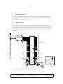
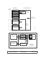
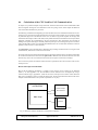
Fig.1 shows a schematic network using the P8xC592 for distributed control applications. The kernel of
each module is a Module Controller (CPU) that communicates via the Bus Controller (i.e. CAN controller)
with the other modules. CPU and CAN controller can also be implemented on the very same chip, as it is
in the P8xC592.
Module 1
Module n
APPLICATION
INTERFACE
APPLICATION
INTERFACE
MODULE
CONTROLLER
P8xC552
APPLICATION
INTERFACE
P8xC592
BUS
CONTROLLER
PCA 82C200
PHYSICAL
INTERFACE
PHYSICAL
INTERFACE
PHYSICAL
INTERFACE
CAN-Bus Line
bu108073.gem
Fig. 1 Example of a "Controller Area Network"
The P8xC592 is a stand-alone high performance microcontroller designed for use in automotive and
general industrial applications. In addition to the 80C51 standard features this device provides a number
of dedicated hardware functions for these applications. It basically combines the functions of the
well-known P8xC552 microcontroller [9] (without I2C hardware) and the PCA 82C200 (Philips Standalone CAN-controller [3]), with some enhanced features.
Philips Semiconductors
Application Note
HKI/AN 91 014
-3-
The CAN-part of the P8xC592 fulfills the complete CAN specification, to provide the following important
features:
o
multi-master operation in a serial communication network with an unlimited number of active
network nodes,
o
programmable data transmission rate, up to 1 Mbit/s,
o
very low probability of undetected errors, due to powerful error handling,
o
40 m maximum distance between two bus nodes at a data transmission rate of 1 Mbit/s, lower
transmission rates allow even longer distances,
o
guaranteed latency time supporting real-time applications.
This Application Note covers the CAN related items of P8xC592 applications. It describes a simple circuit
example for a module in a CAN network. To apply and understand the application examples given in this
document, the reader should be familiar with the Philips P8xC592 data sheet [2].
2.
P8xC592 Features
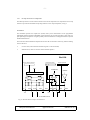
Fig.2 shows the block diagram of the P83C592 (ROM) or the P87C592 (EPROM) versions. There is also
a ROM-less version labeled P80C592 without on-chip program memory. Except the three blocks "CAN
controller", "DMA" and "256 Bytes Aux. RAM", the blocks shown are not different from those which are
present in other 80C51 derivatives like in the well-known Philips P8xC552. The use of the CPU, the
memory access modes, the timers, A/D converter and PWM outputs have already been described in detail
in the User Manual for the P8xC552 [9], which shall not be repeated in this application note again. Please
refer to that document for information about these topics.
VDD
Reset
16K
2
2
PWM
10-Bit ADC
Port 0
(EP)ROM
TX
RX
8-Bit PWM
CAN
Controller
CPU
80C51
256 Bytes
Capt./Comp.
Timer/Counter
Aux. RAM
UART
256 Bytes
DMA
Main RAM
Watchdog
Port 5
bu110151
VSS
Fig. 2 Block diagram of the P8xC592
Philips Semiconductors
Application Note
HKI/AN 91 014
-4-
The CAN controller on the P8xC592 is mainly an on-chip implementation of the Philips Stand-alone
CAN-controller PCA 82C200 [3]. The access to the internal CAN registers now is given via 4 Special
Function Registers (SFR). The transfer of the messages between the CAN controller and the P8xC592’s
main RAM can be done in extremely short time by using Direct Memory Access (DMA). More information
about this feature is given in chapter 4.2.3 .
The P8xC592 has a 256 bytes on-chip auxiliary RAM, which is indirectly addressable in the same way
as external data memory. This doubling of internal RAM capacity satisfies the rising demand for parameter
storage in distributed control applications.
Summarizing the P8xC592 is a single-chip 8-bit microcontroller featuring:
o
80C51 CPU
o
CAN controller with DMA
o
16K bytes ROM / EPROM
o
2 * 256 bytes RAM
o
10-bit A/D converter, 8 channels
o
3 * 16 bit timer/counters
4 capture registers
3 comparators controlling 8 outputs
o
6 * 8-bit I/O ports
o
2 * PWM outputs
o
full-duplex UART
o
interrupt controller (15 sources)
o
watchdog timer
Philips Semiconductors
Application Note
HKI/AN 91 014
-5-
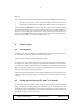
3.
Hardware Aspects
This section covers hardware considerations of a CAN-based module in a network. The first part describes
the minimum circuitry required for the P83C592 / P87C592. The second part gives suggestions for the
connection of the controller to the CAN bus wires.
3.1
Main Circuitry
The P8xC592 is designed to work with a minimum of external components. Fig.3 shows the circuitry of
a CAN node using the ROM- or EPROM- version P83C592 or P87C592. The only additional components
that are required are a crystal (Q1) plus two small capacitors (C1, C2) to drive the on-chip oscillator, a
reset circuit to provide the power-on RESET and a transceiver circuit (see section 3.2) for the connection
to the bus wires.
AV DD
V DD
IC1
CAN_H
CAN_L
TRANSCEIVER
REF
RX1
RX0
TX1
TX0
CV SS
AV SS
digital
I/O
analogue
or
digital
input
+5V
CAN Bus Line
R2
18R
AV DD
C4
100nF
+5V
C5
100nF
55
56
57
24
23
22
21
20
19
18
17
16
REF
CRX1
CRX0
CTX1
CTX0
CV SS
P1.5
P1.4
P1.3
P1.2
P1.1
P1.0
14
13
12
11
10
9
8
7
P4.7
P4.6
P4.5
P4.4
P4.3
P4.2
P4.1
P4.0
62
63
64
65
66
67
68
1
P5.7
P5.6
P5.5
P5.4
P5.3
P5.2
P5.1
P5.0
RD 32
WR 31
P3.5 30
P3.4 29
P3.3 28
P3.2 27
P3.1 26
P3.0 25
3
STADC
59
58
61
60
PWM0 4
PWM1 5
AVref+
AVrefAV DD
AV SS
2 V DD
35 V SS
AD0
AD1
AD2
AD3
AD4
AD5
AD6
AD7
A08
A09
A10
A11
A12
A13
A14
A15
54
53
52
51
50
49
48
47
36
37
38
39
40
41
42
43
PSEN 44
ALE 45
EA 46
digital I/O
or
address/data bus
+5V
digital I/O
Reset
Circuit
+5V
C3
PWM output
47uF
RST 15
EW
6
XTAL1 34
XTAL2 33
R1
C1
Q1
83C592
PLCC-68
8K2
D1
1N4148
33pF
C2
33pF
BU108081.DWG
Fig. 3 P87C592 / P83C592 circuitry for a CAN application
Philips Semiconductors
Application Note
HKI/AN 91 014
-6-
Power Supply
The 5V power supply is split on the different power input pins of the µC. The main supply for the (digital
part of the) CPU is fed to the VDD / VSS pins, buffered by capacitor C5.
It is recommended that the supply AVDD / AVSS for the analogue parts is derived from the main supply
by the filter R2 / C4. The AVDD / AVSS supply is used to drive the on-chip A/D converter and the receiver
section of the CAN controller; it shall also be used for optional biasing of the RX0 / RX1 pins in the
off-chip transceiver.
The pin CVSS is the ground pin belonging to the CAN on-chip transmitter output stages (cf. chapter 3.2.1),
which shall also be used for optional ground potential of the off-chip transceiver.
Program Fetch
The schematics of fig.3 present the circuitry for microcontrollers with on-chip program memory (ROM
or EPROM). Therefore the pin EA is connected to +5V for program being fetched from internal memory.
Note that the EA-pin is only read by the CPU during RESET, that means, switching it during program
execution is not possible. This can give an additional protection against unauthorized copying of the
on-chip program.
Reset Circuit
The schematics of fig.3 present a proposal for a discrete circuit that provides the necessary RESET signal
to the CPU during power-up. The Reset Circuit can be replaced by a connection of the RST-pin to the
power-on/power-fail reset output of the power supply, if available. Note that internal RESET conditions
of the CPU (e.g. watchdog or recover from power-down) may cause the output of a short pulse on the RST
pin, which the Reset Circuit has to tolerate.
3.2
Transceiver: Physical Interface to the Transmission Medium
The transceiver circuit performs the following functions:
o
it converts signals TX0, TX1 into the voltage levels for the bus wires,
o
it converts the voltage levels on the bus wires to be compatible with the CRX0, CRX1 inputs of
the P8xC592.
How this connection actually is implemented, is application-specific. Depending on the requirements for
the bus signals, the transceiver can be realized with more or less effort, the cheapest solution consists only
of a couple of resistors, more expensive ones need some more discrete components or an extra IC. In
principle the very same transceiver circuits can be used as for the stand-alone CAN controller PCA 82C200
[3]. Three examples for cheap discrete transceivers have been described in the Application Note [4] for
the PCA 82C200, for instance.
In order to get to an international standard for CAN communication (including the transceiver), the
International Standardization Organization (ISO) has prepared two standards, one for lower bit rates (up
to 125 kbit/s) [6], one for higher ones [7]. They also define the electrical parameters for the transceiver.
Application hints for implementation of an ISO-compatible transceiver circuit are given in [10].
Philips Semiconductors
Application Note
HKI/AN 91 014
-7-
3.2.1
On-chip Transceiver Components
The off-chip transceiver circuit connects the bus wires to the on-chip transceiver components. The on-chip
transceiver provides the transmitter output stage and the receiver input comparator, see fig.4.
Transmitter
The transmitter provides two output lines (CTX0, CTX1); their characteristics can be programmed
individually with the OUTPUT CONTROL register. Each line can work as open-drain or open-source or
push-pull output, with positive or negative polarity. Thus the transmitter is well prepared to drive any kind
of differential bus lines.
The connections of the transmitter outputs to the bus wires have to be done in such a way, that the resulting
level on the bus is:
o
recessive level, when all nodes transmit a logical 1 or do not transmit,
o
dominant level, when one or more nodes transmit a logical 0.
P8xC592
OUTPUT CONTROL REGISTER
COMMAND REGISTER
TXD
CONTROL REGISTER
COMP OUT
AVDD/2
OUTPUT CONTROL LOGIC
VDD
CTX0
CTX1
CVSS
AVDD
+5V
IN-
CRX0 CRX1
AVSS
REF
bu107302.gem
IN+
+5V
to the CAN bus line
Fig. 4 Structure of the on-chip CAN transceiver
Philips Semiconductors
Application Note
HKI/AN 91 014
-8-
Receiver
The on-chip receiver is a differential input comparator with the input lines CRX0 and CRX1. It decodes
o
the recessive level to a logical 1, when the voltage at the CRX0-pin is higher than at the CRX1-pin,
o
the dominant level to a logical 0, when the voltage at the CRX0-pin is lower than at the CRX1-pin.
Instead of decoding the differential bus signal, the comparator inputs can also be switched by software
to decode the signal of only one of the two bus lines, comparing it to the reference voltage at the REF pin.
The reference voltage can either be provided by the internal on-chip voltage generator (= default), or, if
desired, it is fed to the REF pin by an external source, with the internal source being switched off by
software. The use of single wire decoding is beneficial to continue communication, when one of the two
bus lines has a wiring failure (open or short circuit), please refer to [8].
4.
Software Aspects
4.1
CAN Registers
The P8xC592’s on-chip CAN controller is a full implementation of the CAN protocol. It contains all
necessary features required for a high performance communication protocol.
The CAN controller appears to the CPU as a memory- mapped I/O device which is arranged as Control
Segment, Transmit (Tx) Buffer and Receive (Rx) Buffer (see fig.5).
Exchange of status, control and command signals between the CPU and the CAN controller is done by
the control segment which contains 10 bytes. It is programmed during initialization for configuration of
the communication parameters. Additionally the CPU controls the CAN communication via this segment.
Data to be transmitted are loaded into the Transmit Buffer by the CPU. The buffer contains the descriptor
(Identifier, RTR-bit and DLC) and up to eight data bytes.
After a successful reception messages are read from the Receive Buffer. It consists of two 10 byte memories
which are alternatively used to store messages. The CPU can process one message while another is being
received.
4.2
On-chip Interface Between CPU and CAN Controller
To access the described CAN controller registers, four special function registers CANADR, CANDAT,
CANCON and CANSTA are implemented. All CAN registers of the Control Segment which are used
during communication now appear as being directly addressable as they are represented by these four
special function registers. The Status Register represented by CANSTA now is even bit-addressable. With
the help of these registers and the DMA logic, data transfer between Transmit/Receive Buffers and internal
main RAM is also done very effectively (see fig. 6).
Philips Semiconductors
Application Note
HKI/AN 91 014
-9-
CAN Registers
10
11
12
.
.
.
A
B
C
.
.
.
19
13
20
21
22
.
.
.
14
15
16
.
.
.
29
1D
CONTROL SEGMENT:
CONTROL
COMMAND
STATUS
INTERRUPT
ACCEPTANCE CODE
ACCEPTANCE MASK
BUS TIMING 0
BUS TIMING 1
OUTPUT CONTROL
TEST: do not use
TRANSMIT BUFFER:
identifier (10..3)
identif.(2..0), rtr-bit, dlc
data byte # 1
.
.
.
write
read
read
CANCON
CANSTA
CANCON
Direct access
with SFR
read / write
Access with
CANADR / CANDAT
write
data byte # 8
Access
with DMA
RECEIVE BUFFER 0/1:
identifier (10..3)
identif.(2..0), rtr-bit, dlc
data byte # 1
.
.
.
read
bu107167.gem
address
(dec / hex)
0
1
2
3
4
5
6
7
8
9
Access Modes of the CPU
data byte # 8
Fig. 5 CAN register mapping
CANADR
CANDAT
CANCON
CANSTA
CPU
internal
CPU-bus
Main RAM
RAMaddress
CANaddress
CAN Registers
control
segment
transmit
buffer
CAN
receive
buffer
DMA-control
SFRs
CANdata
DMA-Logic
P8xC592
to other on-chip
peripherals
( CPU-to-CAN interface )
bu109053
Fig. 6 Block diagram of the CPU - to - CAN interface
Philips Semiconductors
Application Note
HKI/AN 91 014
- 10 -
4.2.1
CAN Related Special Function Registers
Table 1 shows the special function register arrangement. Note that CANCON and CANSTA have different
meanings for a read and write access.
SFR
ADR
ACS
MSB
7
CANADR
D8H
R/W
DMA
CANDAT
DAH
R/W
CAND7
CANCON
D9H
R
CANSTA
D8H
3
2
1
LSB
0
reserved AutoInc
CANA4
CANA3
CANA2
CANA1
CANA0
CAND6
CAND4
CAND3 CAND2
CAND1
CAND0
5
CAND5
reserved reserved reserved
R
RX0
active
Bus
Status
W
RAMA7
W
4
6
Wake up Overrun
Int
Int
Error
Int
Transmit Receive
Int
Int
Wake up
Mode
Sleep
Error
Status
Abort Transmit
Clear Release
Overrun Rx Buffer Transm. Request
Transmit Receive TX compl. Tx Buffer
Data Rx Buffer
Status
Status Access Overrun Status
Status
RAMA6
RAMA5
RAM4
RX1
active
RAMA3 RAMA2
RAMA2 RAMA1
HA107221
Table 1: CAN Special Function Registers
CANADR
With the least significant bits CANA4...CANA0 each of the CAN controller internal registers can be
addressed by a write access to CANADR. Reading or modification of the particular CAN register then is
done by reading or writing to CANDAT. CANADR is implemented as a read/write register which also
contains control bits to select auto increment addressing and to start a DMA transfer.
CANDAT
When reading or writing CANDAT, access to the CAN registers addressed by CANADR is possible. The
way of accessing CAN registers via CANADR/CANDAT normally is only necessary for the registers
Acceptance Code, Acceptance Mask, Bus Timing 0, Bus Timing 1, Output Control, which the CPU has
to access during initialization only.
CANCON
CANCON is a register with different meaning for write and read operation. Writing to CANCON is a
direct access to the command register and reading from it is a direct access to the interrupt register.
CANSTA
The bit addressable register allows a direct read access to the Status Register of the CAN Controller.
Writing to CANSTA sets the address of the on-chip main RAM for a subsequent DMA transfer.
Philips Semiconductors
Application Note
HKI/AN 91 014
- 11 -
4.2.2
Auto Address Increment
Fast reading and writing of consecutive CAN Controller internal registers is possible by setting the AutoInc
bit of CANADR and the concerning register address simultaneously. A first access to CANDAT refers to
the register specified in CANADR. After any read or write access to CANDAT the contents of CANADR
are incremented automatically in this mode.
Incrementing CANADR beyond XX111111B resets the AutoInc bit automatically to XX000000B.
4.2.3
High Speed DMA
The DMA logic provides a very fast transfer of complete messages between receive/transmit buffers and
internal data memory (Main RAM) within 2 instruction cycles. The transfer process operates in the
background and therefore the CPU can continue with the next instruction. However, an access to the Main
RAM or to the CAN special function registers is not allowed during this time.
A DMA transfer action is achieved by first writing the RAM address into CANSTA and then writing the
Tx- or Rx-Buffer address and the DMA bit simultaneously into CANADR.
The DMA automatically recognizes the transfer direction (see table 2). For the Rx Buffer DMA there is
the option to copy a whole message or only a part of it.
CANADR
subject to transfer
transfer direction
8AH
whole message
RAM -> Tx Buffer
94H
95H
whole message
whole message
without first byte
data bytes only *)
last data bytes *)
.
.
only the last data byte *)
Rx Buffer -> RAM
96H
97H
.
.
9DH
*) data bytes are copied as far as they are available (DLC!)
Table 2: DMA Modes
Setting the DMA bit causes an automatic evaluation of the data length and subsequent transfer. For a Tx
Buffer DMA transfer the data length is always expected at "RAM address + 1".
After the DMA transfer has been finished, the DMA bit and the AutoInc bit are reset.
Philips Semiconductors
Application Note
HKI/AN 91 014
- 12 -
4.3
Basic Functions for CAN Communication
4.3.1
Initialization
During Initialization the P8xC592’s CAN Controller is configured according to the required communication parameters. Before setting the registers in the Control Segment (see fig.5) first the Reset Request bit
in the Control Register has to be set to "present" (high). An initialization procedure should include
definitions of the following items:
o
Acceptance Filter
o
Bus Timing
o
Output Mode
o
Interrupts
o
Reference Voltage Mode
A flow chart of the initialization procedure is shown in table 4.
When the configuration of the P8xC592 is finished the Reset Request bit has to be set to "absent" to allow
receive- or transmit operations.
4.3.2
Transmission
The CPU may write a message into the transmit buffer whenever the transmit buffer access bit (Status
Register) is set. After writing the message to the transmit buffer and setting the transmission request bit
high (Command Register), the CAN Controller begins with the transmission process.
If the CPU cannot access the transmit buffer because a previously requested message is still waiting for
transmission, it is possible to abort the current process. A transmission already in progress is not stopped.
+------------------------------------------------------------------------------+
|if (status bit TRANSMIT BUFFER ACCESS = "released")
|
+------------then--------------+--------------------else-----------------------+
| write message into
|if (<high priority message to be transmitted>) |
| TRANSMIT BUFFER
+----------------then---------------+----else---+
+------------------------------+ set command bit
|
|
|set command bit TRANSMISSION | ABORT TRANSMISSION:= "present"
|
|
|REQUEST := "present"
+-----------------------------------+-----------+
|
|(* the next transmission is delayed until
|
|
|
TRANSMIT BUFFER ACCESS = "released" is
|
|
|
signalled by a TRANSMIT INTERRUPT or by
|
|
|
polling the STATUS REGISTER *)
|
+------------------------------+-----------------------------------------------+
Table 3: Flow chart of a transmission procedure
Philips Semiconductors
Application Note
HKI/AN 91 014
- 13 -
+------------------------------------------------------------------------------+
|(* start initialization; write CONTROL REGISTER *)
|
|
|
|
- set RESET_REQUEST := "present"
|
|
- set TEST_MODE
:= "disabled"
|
+------------------------------------------------------------------------------+
|(* write acceptance filter *)
|
|
|
|
- write ACCEPTANCE CODE REGISTER
|
|
- write ACCEPTANCE MASK REGISTER
|
|
|
|(* example: contents of ACCEPTANCE CODE REGISTER
=
01110010B
|
|
contents of ACCEPTANCE MASK REGISTER
=
00111000B
|
|
allows for messages with following IDs:
01xxx010xxxB
|
|*)
|
+------------------------------------------------------------------------------+
|(* define bus timing (baud rate on the CAN Bus) *)
|
|
|
|
- write BUS TIMING 0 REGISTER
|
|
- write BUS TIMING 1 REGISTER
|
|
|
|(* example: contents of BUS TIMING 0 REGISTER = 10001001B
|
|
contents of BUS TIMING 1 REGISTER = 11101011B
|
|
results in:
|
|
tSCL
= (9 + 1) * 2 * tOSC
(with fOSC = 16 MHz: 1.25 us) |
|
tSJW
= (2 + 1) * tSCL
(3.75 us) |
|
SAM
= 1
(three samples / bit taken) |
|
tSYNC
= 1 * tSCL
(1.25 us) |
|
tTSEG2
= (6 + 1) * tSCL
(8.75 us) |
|
tTSEG1
= (11 + 1) * tSCL
(15.00 us) |
|
tBIT
= tSYNCSEG + tTSEG1 + tTSEG2 = 20 * tSCL (25.00 us) |
|
variation of bit time due to resynchronization:
|
|
tBITmin = tBIT - tSJW = 17 tSCL
(21.25 us) |
|
tBITmax = tBIT + tSJW = 23 tSCL
(28.75 us) |
|*)
|
+------------------------------------------------------------------------------+
|(* define bus driver characteristics *)
|
|
|
|
- write OUTPUT CONTROL REGISTER
|
|
|
|(* example: contents of OUTPUT CONTROL REGISTER = 10101010B
|
|
results in:
|
|
output mode: normal 1 (bit sequence on TX0 and TX1 pins)
|
|
TX0 configuration: bit-state 0 (1) -> output-state low (float)|
|
TX1 configuration: bit-state 0 (1) -> output-state high (float)|
|*)
|
+------------------------------------------------------------------------------+
|(* end initialization; write to CONTROL REGISTER *)
|
|
|
|
- enable interrupt sources
(* bits 4 .. 1 *)
|
|
- define mode of reference voltage
(* bit 5
*)
|
|
- define the resynchronization mode
(* SYNCH; bit 6 *)
|
|
- set RESET REQUEST := "absent"
(* bit 0
*)
|
+------------------------------------------------------------------------------+
(* = start of comment
*) = end of comment
Table 4: Flow chart of an initialization procedure
Philips Semiconductors
Application Note
HKI/AN 91 014
- 14 -
4.3.3
Reception
Whenever the status bit ’Receive Buffer Status’ is set, a new message is available in the Rx Buffer. Polling
the Status Register enables the information of new message data in the Rx Buffer to be coordinated and
controlled by the CPU.
When the Receive Interrupt is enabled the according bit in the interrupt register is set simultaneously with
the Receive Buffer Status bit and the interrupt service can start with reading of message data from the Rx
Buffer.
After Reading the buffer contents the CPU has to release this buffer by setting the Release Receive Buffer
command bit. This may result in another message becoming immediately available.
+------------------------------------------------------------------------------+
|read message from RECEIVE BUFFER
|
+------------------------------------------------------------------------------+
|set command bit RELEASE RECEIVE BUFFER := "released"
|
+------------------------------------------------------------------------------+
Table 5: Flow chart of a reception procedure
4.3.4
Sleep Mode
If the Sleep Bit of the Command Register is set high the CAN controller enters the Sleep Mode, requiring
that there is no bus activity and no interrupt is pending. A network enters the ’Sleep Mode’ when all its
nodes enter the Sleep Mode.
The CAN Controller wakes up after setting the Sleep bit of the Command Register low or when there is
any bus activity. Upon wake up a wake up interrupt is generated. It is not necessary to enable the wake up
interrupt.
After the CAN Controller entered Sleep Mode the CPU may be set into the ’Power Down Mode’ (oscillator
stopped). Upon wake up, the oscillator is started again. The wake up interrupt will wake up a CPU from
’Power Down Mode’ by generating a Reset pulse, if the SIO1 (CAN) interrupt source was enabled. A
CAN Controller that wakes up because of bus activity is not able to receive this message until it detects a
bus free signal.
Reading of the Sleep bit reflects the status of the CAN Controller.
+------------------------------------------------------------------------------+
|Set command bit SLEEP := "sleep"
|
+------------------------------------------------------------------------------+
Table 6: Flow chart of a "go to sleep" procedure
Philips Semiconductors
Application Note
HKI/AN 91 014
- 15 -
4.3.5
Comparator Switches
Data communication between the nodes of a network is disturbed or stopped when the bus wires are
short-circuited (global failures) or interrupted (local failures). With the P8xC592 precautions have been
taken to continue data communication despite of a bus failure.
With the help of the comparator switches, implemented in the CAN Controller, it is possible to tolerate
the following single wiring failures:
o
one of the bus lines is short-circuited with VBAT or GND
o
one bus line is short-circuited against the other
o
interruption of one of the bus lines
The structure of the on-chip CAN Transceiver in fig.4 shows that in case of a short circuit it is possible to
disconnect a blocked bus wire from the CAN receivers of all network nodes and replace this faulty bus
line potential by a local reference level at one of the comparator inputs. In some cases it might be necessary
to disconnect the bias voltage of one bus wire from the power supply terminal, additionally, to continue
with communication.
Bus line interruptions are solved similar to the short circuit failures by replacing the potential of one bus
line with a local reference potential.
The positions of the switches are defined via the Command Register bits RX0A and RX1A (see table 7).
Reading of RX0A/RX1A reflects the status of the switches.
RX0A
RX1A
Result
0
0
1
1
0
1
0
1
unchanged
IN+ = REF, IN- = CRX1
IN+ = CRX0, IN- = REF
IN+ = CRX0, IN- = CRX1
Table 7: Results of setting RX0A/RX1A
With the help of the described comparator switches three configurations can be selected:
o
two wire communication (differential signal)
o
single wire communication using CAN_H
o
single wire communication using CAN_L
Thereby a test of the bus wires can be implemented easily by software: if single wire communication is
possible in the network with each of the bus lines as well as differential communication, then there is no
wiring failure. Otherwise the faulty wire is detected (diagnosis) and the network may continue to
communicate on the other wire till the faulty wire is repaired.
For more details on CAN Bus failure management please refer to [8].
Philips Semiconductors
Application Note
HKI/AN 91 014
- 16 -
4.4
Control of CAN Communication
Information about the reception of messages, the completion of a transmission, data overrun, error status
etc. can be signalled to the CPU either with interrupt processing, described in chapter 4.4.1 or with polling,
described in chapter 4.4.2. It can be of advantage to mix both, polling and interrupt control. Note, that the
wake up event can only be processed by interrupt.
4.4.1
Interrupts
The P8xC592 controls five different CAN related interrupt sources. These are the Receive-, Transmit-,
Overrun-, Error- and the Wake up Interrupt. All interrupts can be enabled/disabled via the Control Register
except of the Wake up Interrupt which is always enabled. Setting of the interrupt sources is usually done
during initialization (see also table 4). Do not forget to enable the CPU’s SIO1 interrupt (by ES1 bit) and
the global interrupt (by EA bit).
Upon the occurrence of one or more (enabled) interrupts the according bits are set in the Interrupt Register
and a CAN interrupt (SIO1) for the CPU is performed. After reading this register, that appears to the CPU
as a read only memory, all bits are reset by the CAN Controller. Therefore, the Interrupt Register should
be stored in a bitaddressable part of the CPU memory for later interrupt evaluation.
Table 8 shows the procedure for an Interrupt Register data evaluation. In this example it is assumed that
all interrupt sources are enabled to present a complete description.
The following summary gives a short overview of the CAN related interrupts and their occurrences.
Receive Interrupt:
If a new message is available in the Receive Buffer, the Receive Interrupt is
given.
Transmit Interrupt:
A Transmit Interrupt is signalled, when a transmission has been completed
or aborted.
Error Interrupt:
If the Bus Status or the Error Status changes, an Error Interrupt is given.
Overrun Interrupt:
When both Receive Buffers contain a message and the first byte of the next
message should be stored, the Overrun Interrupt is signalled.
Wake up Interrupt:
Whenever the Sleep Mode is left, a Wake up Interrupt is signalled.
When CAN communication is controlled partly in the interrupt service routine and partly in the main
program, care has to be taken about the use of CANADR/CANDAT (indirect addressing of the CAN
Registers) or CANADR/CANSTA (use of DMA), respectively. If they are used as well in main program
level as in interrupt level, it might be necessary to save the address of CANADR (push/pop) during interrupt
processing, or disable the CAN interrupt during DMA transfer at main level, respectively. For the latter,
if required, the interrupt has to be disabled right before the RAM address is written into CANSTA, and
can be re-enabled just after the start of the DMA transfer.
Philips Semiconductors
Application Note
HKI/AN 91 014
- 17 -
+------------------------------------------------------------------------------+
|read INTERRUPT REGISTER and store in the bitaddressable part of the CPU memory|
+------------------------------------------------------------------------------+
|if (WAKE UP INTERRUPT = "set")
|
+-------------------------------then-------------------------------+---else----+
|if ( <CPU state> = "just being awoken")
|
|
+---------------then---------------+-------------else--------------+
|
|(* the network was awoken by some |(* the just issued GOTO SLEEP |
|
|
CAN Bus activity
|
command was not successful |
|
|*)
|*)
|
|
|Perform appropriate network
|Perform appropriate action
|
|
|wake up activities
|
|
|
+----------------------------------+-------------------------------+-----------+
|if (TRANSMIT INTERRUPT = "set")
|
+--------------------------------then---------------------------------+--else--+
|(* the TRANSMIT BUFFER is released *)
|
|
|A next message may be written into the TRANSMIT BUFFER
|
|
+---------------------------------------------------------------------+
|
|if ( <using the ABORT TRANSMISSION command> )
|
|
+-----------------------then--------------------+----------else-------+
|
|if ( TRANSMISSION COMPLETE STATUS = "complete")|(* last requested
|
|
+--------then----------+---------else-----------+
transmission has |
|
|(* last requested
|(* last requested
|
been completed
|
|
|
transmission has
|
transmission has not |*)
|
|
|
been completed,
|
been completed;
|
|
|
|
no ABORT TRANSMISS-|
the ABORT
|
|
|
|
ION command has
|
TRANSMISSION command |
|
|
|
been executed *)
|
was successful *)
|
|
|
+----------------------+------------------------+---------------------+--------+
|if (RECEIVE INTERRUPT = "set")
|
+---------------------------------then---------------------------------+-else--+
|read RECEIVE BUFFER into CPU memory
|
|
+----------------------------------------------------------------------+
|
|set command bit RELEASE RECEIVE BUFFER := "released"
|
|
+----------------------------------------------------------------------+
|
|if (OVERRUN INTERRUPT = "set")
|
|
+-----------------------------then-----------------------------+-else--+
|
|an application may use this information to change its
|
|
|
|behaviour (e.g. faster reaction on a RECEIVE INTERRUPT)
|
|
|
+--------------------------------------------------------------+
|
|
|set command bit CLEAR OVERRUN := "clear"
|
|
|
+--------------------------------------------------------------+-------+-------+
|if (ERROR INTERRUPT = "set")
|
+---------------------------------then---------------------------------+-else--+
|if ( BUS STATUS = "on-bus ")
|
|
+--------------then---------------+---------------else-----------------+
|
|(* P8xC592 takes part in bus
|(* P8xC592 does not take part in
|
|
|
activities
|
bus activities
|
|
|*)
|*)
|
|
|if ( ERROR STATUS = "ok" )
|if ( <restart CAN required> )
|
|
+------then------+-----else-------+--------then---------+-----else-----+
|
|(* the CAN Bus |(* the CAN Bus |set control bit
|(*
|
|
|
is presently |
is presently |RESET REQUEST :=
| CAN hardware |
|
|
not severely |
severely
|"absent"
| is left in
|
|
|
disturbed
|
disturbed
|(* now the P8xC592
| "off-bus" and|
|
|*)
|*)
|
waits for 128 * 11| "reset" state|
|
|
|
|
consecutive
|*)
|
|
|
|
|
recessive bits
|perform appli-|
|
|
|
|
before going
|cation-specif.|
|
|
|
|
"on-bus" again
|default-mode |
|
|
|
|*)
|operation
|
|
+----------------+----------------+---------------------+--------------+-------+
Table 8: Flow chart of Interrupt Register data evaluation
Philips Semiconductors
Application Note
HKI/AN 91 014
- 18 -
4.4.2
Polling
Analysing the contents of the Status Register, as shown in table 9, is very similar to analysing the contents
of the Interrupt Register. With the following overview the concerning Status bits are described:
Receive Buffer Status:
This bit is set when a new message is available.
Transmit Buffer Access:
The CPU may write a message to the Tx Buffer when this bit is set.
Error Status:
The Error Status bit is set when at least one of the Error Counters has reached
the warning limit.
Data Overrun:
When both Receive Buffers are full and the first byte of a new message should
be stored, this bit is set.
+------------------------------------------------------------------------------+
|if (TRANSMIT BUFFER ACCESS = "released")
|
+--------------------------------then---------------------------------+--else--+
|a next message may be written into the TRANSMIT BUFFER
|
|
+---------------------------------------------------------------------+
|
|if (<using the ABORT TRANSMISSION command>)
|
|
+----------------------then---------------------+--------else---------+
|
|if (TRANSMISSION COMPLETE STATUS = "complete") |(* last requested
|
|
+--------then--------+------------else----------+
transmission has |
|
|(* last requested
|(* last requested
|
been completed
|
|
|
transmission has |
transmission has not
|*)
|
|
|
been completed, |
been completed due to |
|
|
|
no ABORT TRANS- |
an ABORT TRANSMISSION |
|
|
|
MISSION command |
command
|
|
|
|
has been exec. *)|*)
|
|
|
+--------------------+--------------------------+---------------------+--------+
|if (RECEIVE BUFFER STATUS = "full")
|
+---------------------------------then---------------------------------+-else--+
|read RECEIVE BUFFER into CPU memory
|
|
+----------------------------------------------------------------------+
|
|set command bit RELEASE RECEIVE BUFFER := "released"
|
|
+----------------------------------------------------------------------+
|
|if (DATA OVERRUN = "overrun")
|
|
+-----------------------------then-----------------------------+-else--+
|
|an application may use this information to change its
|
|
|
|behaviour (e.g. faster reaction on a RECEIVE INTERRUPT)
|
|
|
+--------------------------------------------------------------+
|
|
|set command bit CLEAR OVERRUN := "clear"
|
|
|
+--------------------------------------------------------------+-------+-------+
|if (BUS STATUS = "on-bus")
|
+----------------then-----------------+------------------else------------------+
|(* P8xC592 takes part in bus
|(* P8xC592 does not take part in bus
|
|
activities
|
activities
|
|*)
|*)
|
|if (ERROR STATUS = "ok")
|if (<restart CAN hardware required>)
|
+-------then-------+-------else-------+----------then----------+-----else------+
|(* the CAN-bus is |(* the CAN-bus is |set control bit RESET
|perform
|
|
presently
|
presently
|REQUEST := "absent"
|application|
|
not severely
|
severely
|
|specific
|
|
disturbed
|
disturbed
|(* now the P8xC592
|default-mode
|
|*)
|*)
|
waits for 128 * 11
|operation
|
|
|
|
consecutive
|
|
|
|some application- |
recessive bits
|
|
|
|specific actions |
before going
|
|
|
|may be necessary |
"on-bus" again
|
|
|
|
|*)
|
|
+------------------+------------------+------------------------+---------------+
Table 9: Flow chart of Status Register data evaluation (polling)
Philips Semiconductors
Application Note
HKI/AN 91 014
- 19 -
4.5
CPU Load for CAN - a Real Example
In a CAN system data transfer can be done with a very high level of safety with the CAN controller part
of the P8xC592. The CPU has only the task of post-processing the received data and pre-processing the
data to be transmitted. Communication between CPU and CAN controller is easily done via the Special
Function Registers described in chapter 4.2.1. Using the DMA transfer facility, data exchange between
CPU and Rx/Tx buffer is very effective.
That means that the resulting CPU load for CAN communication is very low, as the analysis of the
following communication example proves. Simulations with "NetSim" (a simulator for CAN
communication, see chapter 5.4) have been done with a real communication example of 7 nodes. At a data
rate of 500kbit/s, 12 different messages M are transferred on the bus. Fig.7 shows the structure of the
network. M3_2 means: 2nd type of message that is transmitted by node number 3, for instance.
Node1
Node2
Node3
Node4
M1_1
M2_1
M2_2
M3_1
M3_2
M4_1
M4_2
CAN Bus
Node5
Node6
Node7
M5_1
M5_2
M6_1
M6_2
M7_1
HA107161
Fig. 7 Network example
The communication matrix and information about message length, repetition time and node numbers are
given in table 10, whereby the described communication of the example with the according messages
results in a total bus load of about 23%.
The CPU load for CAN communication is defined as the percentage of time the CPU is serving the CAN
communication; its calculation is described in detail in chapter 4.6.
The diagram of figure 8 shows the CPU load of nodes 1...7, split up in receive and transmit actions of the
CPU. Receive actions are executed for all messages that pass the acceptance filter. These messages are
copied into the CPU RAM except they are not of interest for the CPU, the latter means they are rejected.
The result of this simulation is that the CPU spends only 3.4% of the time for CAN related procedures. In
this example 96.6% of the time is free for other CPU activities.
Philips Semiconductors
Application Note
HKI/AN 91 014
- 20 -
Transmitting
node /
DLC
message
ID
Repetition
Time
[ms]
1
M1_1
4
2
2
M2_1
M2_2
3
3
receiving node
1
2
3
4
5
6
7
10
2
-
x
x
x
-
-
x
7
2
11
30
2
100
x
-
-
x
-
x
-
x
-
x
-
x
x
M3_1
M3_2
5
3
15
31
20
100
x
-
x
-
-
-
x
-
-
x
x
4
4
M4_1
M4_2
5
3
32
33
20
100
-
x
-
-
-
-
x
-
x
x
5
5
M5_1
M5_2
8
8
20
34
100
100
x
-
x
-
x
-
-
-
x
-
x
x
6
6
M6_1
M6_2
8
8
21
35
100
100
-
x
-
-
x
-
x
-
-
x
x
7
M71
8
36
100
-
-
-
-
x
x
-
Table 10: Communication Matrix of the network example. (ID = Identifier, DLC = data length code)
CPU Load
[%]
97
96.6%
96
3
2.61%
2
HA110151
1
0.61%
0.18%
0
Copy
Reject
Receive
Transmit
Other
Fig. 8 CPU load (Average of nodes 1 . . . 7)
Philips Semiconductors
Application Note
HKI/AN 91 014
- 21 -
4.6
Calculation of the CPU Load for CAN Communication
In chapter 4.5 a practical example was presented for which the CPU load for CAN communication had
been investigated. The figures were obtained for a real set-up using 7 nodes. In this chapter the details of
such a CPU load calculation are presented.
The following calculations and diagrams give hints and ideas to the user of the P8xC592 about the receive
interrupt service execution time and CPU load when serving the CAN controller. To get results as reliable
as possible all figures are calculated for worst case. As shown in fig.8 both reception of messages and
transmission of messages result in CPU load, but the partial CPU load for transmission obviously is almost
negligible. Therefore the considerations in the next sections have been focussed on the reception of
messages. Reception of messages is normally initiated by interrupt. The according interrupt service routine
copies the Rx buffer contents to an internal CPU RAM location. Its execution time should be as short as
possible in order to achieve a low CPU load.
The CPU load for CAN communication is defined as the percentage of time the CPU is serving the CAN
communication, measured in a time interval of interest.
In case the time interval is shorter than the duration of a message transfer on the bus, the Spare Time should
be considered instead of the CPU load. The Spare Time is defined as the amount of coherent CPU time
the CPU may reserve for non-CAN activities between the reception of consecutive messages.
The next section presents the software which meets the requirements for a fast execution of the receive
interrupt service.
Receive Interrupt Service Routine
Base of all the following calculations is a simple receive interrupt service routine for the P8xC592
(table 11, see also Appendix A.1). The calculations of CPU load have been investigated by using a
reference software (fig.9, Appendix A.1) that uses the receive interrupt service routine. It also checks the
data overrun condition in order to evaluate the Spare Time. The described software and the results are an
example and transformation to user specific requirements is very easy.
Init P8xC592
Receive Interrupt
Service Routine
Main Loop
LED
Indication
Overrun Loop
HA110163
Fig. 9 Reference software with Receive Interrupt Service Routine
Philips Semiconductors
Application Note
HKI/AN 91 014
- 22 -
First of all the arrangement of the reference software is given in a short summary:
Identifier:
ID10,ID9,ID8,ID7 are fixed by acceptance filter,e.g. ID = 0101 XXXX XXX
Interrupts:
Receive Interrupt enabled
Data Copy:
data bytes according data length code and a part of the identifier (as an
indication for a new message) are copied into the internal µC Main RAM
Remote Frames:
in case of remote frame reception the data length code is deleted and only a
part of the identifier is copied as an indication of its reception.
Overrun:
the overrun status bit is checked in the main loop. Whenever an overrun
condition would be detected, indication would be done via LED. The program
remains in the overrun loop until reset.
Reject:
Messages which pass the acceptance filter, but are useless for the µC, are
rejected by the software automatically.
CAN_INTERRUPT:
context switch
save Accu & PSW
select register bank
clear interrupt bits (read Interrupt Register)
calculate table address
fetch target address from table
if target address ≠ 0, then
copy Rx Buffer to int. µC RAM starting at target address
release Receive Buffer
(Acknowledge)
restore context
Table 11: Flowchart of the Receive Interrupt Service Routine
Receive Interrupt Execution Time
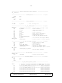
Table 12 shows the interrupt execution time for the used receive interrupt service routine. The routine is
split up into different macros, for each of them the according processing time has been calculated.
The receive interrupt execution time is shorter, when a message has to be rejected. Therefore two columns
are shown, the particular processing time for the copy and the reject case. Another column shows the time
passing until the Receive Buffer is released, for evaluation of the CPU Spare Time (see chapter 4.6.2).
Times are given in units of machine cycles and one cycle consists of 12 oscillator periods. The used
oscillator frequency of the P8xC592 is 16 MHz resulting in a cycle time of 0.75µs.
Fig. 10 shows the receive interrupt execution time ("copy" and "reject") as a function of the message data
length code (DLC). For purpose of comparison also the message transfer time on the bus is given for the
data rates: 250kbit/s, 500kbit/s and 1Mbit/s.
Philips Semiconductors
Application Note
HKI/AN 91 014
- 23 -
Macro Name
Machine
Cycles
Copy
Reject
Rx Buff
Release
Max. Interrupt
Response Time
5
x
x
x
Long Jump to
Interrupt Service Routine
2
x
x
x
Context Switch
6
x
x
x
Clear Int. Bits
1
x
x
x
Calculate Target Address
15
x
x
x
Copy rx buffer
8
x
-
x
Acknowledge
2
x
x
x
Restore Context
6
x
x
-
45
37
39
Sum of cycles
Table 12: Summary of receive interrupt execution times (machine cycles)
Fig. 10 shows that due to the DMA function of the P8xC592 the receive interrupt execution time is always
independent of the length of the received message. It is very important that the receive interrupt execution
time is much shorter than the time the message itself spends on the bus. This clearly shows that a data
overrun caused by a burst of messages can be excluded.
Message(250kbit/s)
250
time
Message
(500kbit/s)
us
200
150
Message
(1Mbit/s)
100
50
COPY
REJECT
0
HA110152
0
1
2
3
4
5
6
7
8
Data Length Code
Fig.10
Receive interrupt execution time ("copy" and "reject") and message transfer time ("Message")
for 16MHz CPU as a function of Data Length Code
Philips Semiconductors
Application Note
HKI/AN 91 014
- 24 -
4.6.1
CPU Load
Three parameters are important for the calculation of the CPU load while receiving messages: The used
receive interrupt execution time (see tables 11/12), the bit rate and the bus load.
The bus load is the percentage of time the bus is occupied (active) by transferring messages. Therefore it
has to be calculated how many messages are transferred in a time interval, and how long a message transfer
is on the bus. The latter is the message length (=number of bits) multiplied by the time of one bit. The
message length depends on the data length code. For the following calculations a data length code
estimation has to be made.
bus load =
bus active time
number of messages ⋅ message length ⋅ bit time
=
time interval
time interval
In order to get a direct relation between CPU Load, bit rate and bus load, from the formula for the bus load
the formula for the number of messages is derived, which can be inserted into the definition of the CPU
load:
number of messages =
bus load ⋅ time interval
message length ⋅ bit time
CPU load =
number of messages ⋅ receive interrupt execution time
time interval
CPU Load =
bus load ⋅ time interval ⋅ receive interrupt execution time
message length ⋅ bit time ⋅ time interval
With the definition of bit rate = 1 / bit time we get
CPU load = bus load ⋅ bit rate ⋅
receive interrupt execution time
= bus load ⋅ bit rate ⋅ τ
message length
The result is, that the CPU load is proportional to the bus load and bit rate. The term τ := receive interrupt
execution time / message length only depends on the data length code, as it is shown in fig. 11.
Using this formula the CPU load can be calculated for any bit rate at any bus load: for example, a bus load
of 10% a t 400kbit /s wit h onl y one-byt e me ssages (copy al l of the m) mea ns
10% ⋅ 0.4 Mbit/s ⋅ 0.6 µs/bit = 2.4% of CPU load. For the example of 4-byte messages (DLC=4) the CPU
load has been calculated for different bit rates and different bus loads, the result is shown in table 13.
Philips Semiconductors
Application Note
HKI/AN 91 014
- 25 -
0.7
s
0.6
bit
0.5
Copy
0.4
Reject
0.3
0.2
HA110172
0
=
1
2
receive interrupt execution time
message length
3
4
5
6
7
8
Data Length Code
Fig. 11 Diagram for calculation of the CPU load while receiving messages
bit rate
10 % bus load
20 % bus load
50 % bus load
100 kbit/s
0.4 %
0.8 %
2.1 %
250 kbit/s
1.0 %
2.1 %
5.2 %
500 kbit/s
2.1 %
4.2 %
10 %
1 Mbit/s
4.2 %
8.4 %
21 %
Table 13: CPU load when 4-byte messages (DLC=4) are used, for worst case (copy all of them)
4.6.2
Spare Time
But, what happens when the CAN interrupt is delayed or interrupted (e.g. by other interrupt service routines
with same or higher priority) ? The first statement is, that the CAN receive interrupt can be delayed for at
least that amount of time that is the difference between message transfer time and the receive interrupt
execution time.
The actual time that a CAN receive interrupt service may be delayed without risk of loosing a message
("data overrun") is even longer: In fig.12 the execution of the receive interrupt service routine has been
delayed so that the routine is not yet finished when the next message comes in, but the ’Release Receive
Buffer’ command comes just in time before the first byte of the next message is to be stored in the Receive
Buffer. No message is lost, but of course that long delay must be compensated by faster response for
subsequent reception.
Philips Semiconductors
Application Note
HKI/AN 91 014
- 26 -
message n
( DLC = ? )
-> RX Buffer 0
#bits:
message n+2
( DLC = ? )
-> RX Buffer 0
message n+1
( DLC = 0 )
-> RX Buffer 1
3
44
3
SOF +
7 Identifier bits
3
t
delay
receive interrupt execution time
here receive interrupt
for message n
latest possibility for the
"release receive buffer"
command for RX buffer 0
becomes active
time for reception of message n
= 3 + 44 + 3 + 8 bit times = 58 bit times
(no stuff bits)
Fig. 12
HA110161
Delay of receive interrupt service. The worst case is, when a message is followed by a 0-byte
message plus another message of any DLC.
The resulting allowed spare time (worst case) is shown in fig.13 for different bit rates. It has been calculated
by relating the Receive Buffer Release time of table 12 (39 cycles) to the transmission time of a 0-byte
message plus the first byte of a next message (58 bits).
time
us
16MHz CPU
250
200
150
100
50
0
0,0
0,2
0,4
0,6
0,8
1,0
bit rate
HA110171
Mbit/s
Fig. 13 Worst case spare time
Philips Semiconductors
Application Note
HKI/AN 91 014
- 27 -
5.
Development Tools
For the P8xC592 several powerful support tools can be supplied to assist during the design and test phase.
These tools are:
o
the P8xC592 Evaluation Board
o
P8xC592 In-Circuit Emulators
o
P87C592 EPROM programmers
o
debug tools for CAN communication
NetSim NetAna NetEmu
5.1
Philips P8xC592 Evaluation Board
The P8xC592 evaluation board (OM4239) is a most versatile aid consisting of a ready-to-use hardware
and software module very similar to a real CAN bus node. The P8xC592 evaluation board can be used in
a car since it has its own 5V supply. An RS232 interface allows the P8xC592 evaluation board to be
connected to a terminal or to a PC with terminal emulating software.
Terminal / PC
12V
Display
Connector
Power
Supply
RS232
Interface
Wrap
P8xC592
32k EPROM
32k SRAM
Field
(on-chip CAN)
P8xC592-Evaluation-Board
Philips Components (c) 1990
Physical
Layer
bu107166.gem
Application
Interface
CAN Bus Wires
Fig. 14 P8xC592 Evaluation Board
Philips Semiconductors
Application Note
HKI/AN 91 014
- 28 -
5.1.1
P8xC592 Evaluation Board Hardware
The P8xC592 evaluation board hardware (single EURO format size) is shown in figure 14. It consists of:
o
P87C592 microcontroller with an external memory capacity of 32 KBytes for RAM and
32 KBytes for ROM storage. Together with the on-chip EPROM there are 48 KBytes of
continuous program memory
o
5V power supply with protection against car battery voltage fluctuations
o
off-chip transceiver circuit, designed to meet ISO/TC 22/SC 3 N608E, with two selectable options:
very low standby power consumption
support of single wire communication to recover from wiring failures.
o
RS232 interface
o
removable LED unit for demonstration purposes
o
wrap field for the user’s specific circuitry
5.1.2
P8xC592 Evaluation Board Software
The software for the P8xC592 evaluation board is stored in the on-board EPROM. The software is designed
to assist users with different experience in CAN-based networks:
o
A user with little experience is able to activate the demonstration software. A menu-driven
software monitor allows the contents of the P87C592’s CAN-registers to be altered and thereby
enables the user to gain experience. For the latter an RS232-terminal (e.g. VT100) is required.
o
A user with more experience will use the "download" facility; this allows the user to load new
software on to the P8xC592 evaluation board. Download requires a PC with terminal emulating
software.
The P8xC592 evaluation board is also ready to be used as a bus monitor, receiving messages from the bus
for display on a terminal.
5.2
In-Circuit-Emulators
For the software development on the P8xC592 several in-circuit-emulators (ICE) are available.
5.2.1
Philips Stand-alone Debug System (SDS)
Philips’ well known and well accepted stand-alone debug station (SDS) for the real-time development of
8-bit µCs is already prepared for future probes > 16MHz. Three configurations are possible:
o
stand-alone operation together with a terminal
o
connected to a terminal plus a host computer (download/upload)
o
connected to a PC/AT (IBM or compatible) with terminal emulation software.
Philips Semiconductors
Application Note
HKI/AN 91 014
- 29 -
Features of the SDS:
o
fully transparent real-time emulation
o
allows optimal emulation according to the exact specification of the target controller
o
emulation memory: 64 KBytes with no wait states
o
interfaces to external equipment
o
full assembly-level debugging
o
HLL debugging possible
o
single step and breakpoint setting
o
trace and triggering with hardware qualifiers
o
trace memory 2048 lines
o
new improved handbook
o
probes for
optimal connection to the target system
optimal emulation of the target µC.
For emulation of the P8xC592 the user needs the following parts:
o
SDS80C51 stand-alone debug system (OM4120S)
o
probe base (OM4110)
o
emulation head "592" (OM4112)
Software for development support with the SDS (assembler, PL/M-compiler, C-compiler, HLL debugger)
is offered and supported by
Tasking B.V.
Plotterweg 31
3821 BB Amersfoort, Netherlands
their products can also be ordered via Philips.
5.2.2
ICE from Other Vendors
Philips supports all major third-party ICE suppliers with emulating chips for the P8xC592. Most of them
already announced to support the P8xC592.
5.3
Programming Support for P87C592 (EPROM)
Philips offers a low-cost programmer for microcontrollers inclusively the P87C592:
o
LCPX5X40 programmer (OM4232)
87C592-PLCC68 adaptor (OM4235)
Philips Semiconductors
Application Note
HKI/AN 91 014
- 30 -
5.4
Debug Tools for CAN Communication
In addition to the P8xC592 evaluation board three other sophisticated development and debug tools for
CAN communication can be supplied. These are offered and supported by
Gesellschaft für Informatik und Mikro-Elektronik
Prof. Dr.-Ing. W.Lawrenz mbH
Ferdinandstr. 15 A
3340 Wolfenbüttel
Germany
NetSim
NetSim (Network Simulator) is a software simulator for use with a Personal Computer. The CAN network
is described using NetSim on the PC by:
o
number of network nodes
o
data transmission rate
o
message identifiers / message length / message transmission repetition rate
o
noise
The simulation is then started. NetSim provides information for various parameters, such as:
o
message delays
o
bus load
NetSim assists during the design phase to investigate these parameters.
NetAna
NetAna (Network Analyzer) is a combined hardware / software tool, operating in conjunction with a PC.
NetAna has two basic functions:
o
to monitor the bus traffic and store the data on the hard disk in the PC for subsequent analysis
o
an event is triggered (identifier, bus error, etc.) and the messages around the trigger point are
recorded.
NetAna assists to trace communication failures in an existing CAN network
NetEmu
NetEmu (Network Emulator) enables the user to transmit defined messages into an operational CAN
network. The resultant network response can then be analyzed by NetAna.
Philips Semiconductors
Application Note
HKI/AN 91 014
- 31 -
6.
References
[1]
CAN Specification Version 1.2, Philips Components 1990
[2]
P8xC592 target device specification, Version 2.2, Philips Export B.V. 1991
[3]
Data sheet PCA 82C200 Stand-alone CAN-controller, Philips Export B.V. 1990,
12NC: 9397 285 30011
[4]
Application of the PCA 82C200 CAN Controller (PSCC), Philips Export B.V. 1990,
12NC: 9398 373 50011
[5]
Bit Timing Parameters for CAN Networks, Application Note KIE07/91ME, Philips Components
PCALH 1991
[6]
Road vehicles - Serial data communication for automotive application. Part 1: Controller Area
Network (CAN). ISO/DIS 11519 part 1, International Organization for Standardization 1992
[7]
Road vehicles - Interchange of digital information - Controller Area Network (CAN) for high
speed communication. ISO/DIS 11898, International Organization for Standardization 1992
[8]
CAN bus failure management using the P8xC592 microcontroller, Application Note
HKI/AN 91 020, Philips Semiconductors PCALH 1991
[9]
Single-chip 8-bit microcontrollers: PCB83C552 - User Manual, Philips Export B.V. 1988,
12NC: 9398 637 90011
[10]
CAN Physical Layer Concepts for the P8xC592 Microcontroller, Application Note HKI/AN 91
027, Philips Semiconductors PCALH 1991
Philips Semiconductors
Application Note
HKI/AN 91 014
- 32 -
Appendix
A. Reference software for investigation of the CPU load
A.1 Receiver part
This module is a program including a very fast, versatile receive interrupt
service routine which is able to handle up to 128 identifiers. It runs on the
P8xC592 Evaluation Board (OM4239), for instance. With only little modifications
it can be adapted to other applications.
The receive interrupt execution time is less than 34µs and every software reject
is done within 28µs.
The acceptance filter of the CAN part is set to 0101 XXXX XXX. Upon reception
of a message which passes the acceptance filter, the data bytes (plus the second
byte of the Rx buffer for signalling the reception of new data to the main
program) are copied into the internal RAM of the P8xC592, according to a table.
In this table for each message the corresponding RAM address can be found or
a "0", telling that the message is not of interest and shall be rejected.
In case of an overrun condition, indication is done via LED.
CONTROL
COMMAND
STATUS
INTERRUPT
ACCEPTANCE_CODE
ACCEPTANCE_MASK
BUS_TIMING_0
BUS_TIMING_1
OUTPUT_CONTROL
EQU
EQU
EQU
EQU
EQU
EQU
EQU
EQU
EQU
0H
1H
2H
3H
4H
5H
6H
7H
8H
CANADR
CANDAT
CANCON
CANSTA
EQU
EQU
EQU
EQU
0DBH
0DAH
0D9H
0D8H
AUTO_RX_BUFFER
RX_BUFFER
DMA_RX_BUFFER
EQU
EQU
EQU
34H
14H
94H
INT_MASK
EQU
00000010B
ES1
BIT
0ADH
DSEG AT 30H
ARRAY_LONG: DS
ARRAY_SHORT:DS
; Rx Interrupt enabled
9
1
; space for Rx of an 8-byte message
; space for Rx of a 0-byte message
BIT_VAR SEGMENT DATA BITADDRESSABLE
RSEG
BIT_VAR
INT_SAVE:
DS
1
RX_INT BIT INT_SAVE.0
CSEG AT RESET
LJMP
MAIN_PROG
CSEG AT 2BH
LJMP
CAN_INTERRUPT
Philips Semiconductors
Application Note
HKI/AN 91 014
- 33 -
MAIN SEGMENT CODE
RSEG
MAIN
MAIN_PROG:
------------------------- Initialization -------------------------------MOV
SP,#7FH
; set stackpointer
CLR
SETB
EA
ES1
; disable all interrupts
; CAN Controller interrupt enabled
MOV
MOV
MOVX
DPTR,#4000H
A,#0FFH
@DPTR,A
; LEDs - dark
MOV
MOV
ARRAY_LONG,#0
ARRAY_LONG+1,#0
; delete RAM position
MOV
INT_SAVE,#0
; delete interrupt save register
CANADR,#CONTROL
CANDAT,#00000001B
; reset request
INIT_CAN:
MOV
MOV
MOV
JNB
A,CANDAT
ACC.0,INIT_CAN
; repeat reset, if reset request is
; absent
MOV
MOV
CANADR,#ACCEPTANCE_MASK
CANDAT,#0FH
MOV
MOV
CANADR,#ACCEPTANCE_CODE ; ID = 0101 XXXX XXX
CANDAT,#05FH
MOV
MOV
CANADR,#BUS_TIMING_0
CANDAT,#80H
MOV
MOV
CANADR,#BUS_TIMING_1
CANDAT,#23H
MOV
MOV
CANADR,#OUTPUT_CONTROL
CANDAT,#0FAH
MOV
MOV
CANADR,#CONTROL
A,CANDAT
ORL
ANL
MOV
A,#INT_MASK
A,#11111110B
CANDAT,A
; enable receive interrupt
; reset request bit = 0
SETB
EA
; enable all interrupts
LOOP:
JB
SJMP
CANSTA.1,OVERRUN
LOOP
OVERRUN:
MOV
MOV
MOVX
A,ARRAY_LONG
DPTR,#4100H
@DPTR,A
; first byte of message to green LED
MOV
MOV
MOVX
A,ARRAY_LONG+1
DPTR,#4200H
@DPTR,A
; second byte of message to red LED
SJMP
$
Philips Semiconductors
Application Note
HKI/AN 91 014
- 34 -
---------------- Receive Interrupt Service Routine
---------------------
CAN_INTERRUPT:
---------------------------- CONTEXT_SWITCH ----------------PUSH
PUSH
USING 1
SETB
CLR
ACC
PSW
RS0
RS1
---------------------------- CLEAR_INTERRUPT ---------------CLR_INT:
MOV
6 cycles -
A,CANCON
1 cycle
-
; clear interrupt bits
-------------------------- RX_INT_TARGET_ADDR --------------- 15 cycles BEGIN_RX:
MOV
MOV
ANL
MOV
MOV
MOV
ANL
RR
ORL
ADD
MOVC
TABLE_BASE:
JZ
CANADR,#AUTO_RX_BUFFER
A,CANDAT
A,#0FH
R1,A
A,CANDAT
R5,A
A,#0E0H
A
A,R1
A,#TABLE-TABLE_BASE
A,@A+PC
;
;
;
;
set auto incr. and CANA = 20dec
fetch RX buffer
upper 4 bits masked per
acceptance filter
;
;
;
;
;
fetch RX buffer+1
temp. save of RX buffer+1
ID2,ID1,ID0,0,0,0,0,0
0,ID2,ID1,ID0,0,0,0,0
0,ID2,ID1,ID0,ID6,ID5,ID4,ID3
; accu contains the target address
RELEASE_BUF
; software reject - no data copying
---------------------- RX_INT_COPY_DATA_LOOP_DMA -----------MOV
MOV
JNB
MOV
ANL
DMA_START:
MOV
NOP
NOP
CANSTA,A
A,R5
ACC.4,DMA_START
CANADR,#RX_BUFFER+1
CANDAT,#0F0H
;
;
;
;
;
;
8 cycles -
target address for DMA
get RX Buffer+1
test of RTR bit
in case of a Remote Frame:
delete data length code,
only the descriptor byte is copied
CANADR,#DMA_RX_BUFFER+1
; wait for data transfer
---------------------------- RX_INT_ACKN -------------------- 2
RELEASE_BUF:
MOV
CANCON,#4
cycles -
; release receive buffer
-------------------------- RESTORE_CONTEXT ----------------- (6) cycles END_RX:
POP
POP
RETI
PSW
ACC
-------------------- RX_INT_TARGET_ADDRESS_TABLE -----------------------TABLE:
DB
DB
DB
DB
DB
DB
DB
DB
; copy data of message 01010101000 to ARRAY_LONG (8+1 bytes)
; copy data of message 01010101010 to ARRAY_SHORT (0+1 byte)
0,0,0,0,0,ARRAY_LONG,0,0,0,0,0,0,0,0,0,0 ; ID2=0,ID1=0,ID0=0
0,0,0,0,0,0,0,0,0,0,0,0,0,0,0,0
; ID2=0,ID1=0,ID0=1
0,0,0,0,0,ARRAY_SHORT,0,0,0,0,0,0,0,0,0,0; ID2=0,ID1=1,ID0=0
0,0,0,0,0,0,0,0,0,0,0,0,0,0,0,0
; ID2=0,ID1=1,ID0=1
0,0,0,0,0,0,0,0,0,0,0,0,0,0,0,0
; ID2=1,ID1=0,ID0=0
0,0,0,0,0,0,0,0,0,0,0,0,0,0,0,0
; ID2=1,ID1=0,ID0=1
0,0,0,0,0,0,0,0,0,0,0,0,0,0,0,0
; ID2=1,ID1=1,ID0=0
0,0,0,0,0,0,0,0,0,0,0,0,0,0,0,0
; ID2=1,ID1=1,ID0=1
END
Philips Semiconductors
Application Note
HKI/AN 91 014
- 35 -
A.2 Transmitter part
----------------------------- Tx Procedure --------------------------------This module is a program including a transmit procedure using a loop that copies
data from the internal µC RAM to the Tx buffer of the P8xC592. It runs on the
P8xC592 Evaluation Board, for instance. Whenever the controller gets bus access,
the contents of the buffer is transmitted on the CAN bus. Therefore it generates
a very high bus load. The Identifier of the message has been chosen such, that
it will be received by the reference software (see Appendix A.1).
CONTROL
COMMAND
STATUS
INTERRUPT
ACCEPTANCE_CODE
ACCEPTANCE_MASK
BUS_TIMING_0
BUS_TIMING_1
OUTPUT_CONTROL
EQU
EQU
EQU
EQU
EQU
EQU
EQU
EQU
EQU
0H
1H
2H
3H
4H
5H
6H
7H
8H
CANADR
CANDAT
CANCON
CANSTA
EQU
EQU
EQU
EQU
0DBH
0DAH
0D9H
0D8H
DMA_TX_BUFFER
EQU
8AH
DSEG AT 30H
ARRAY:
DS
10
CSEG AT RESET
LJMP
MAIN_PROG
MAIN SEGMENT CODE
RSEG
MAIN
MAIN_PROG:
---------------------------- Initialization ----------------------------MOV
SP,#7FH
; set stackpointer
CLR
EA
; disable all interrupts
MOV
MOV
MOVX
DPTR,#4000H
A,#0FFH
@DPTR,A
; LEDs - dark
MOV
MOV
ARRAY+0,#01010101B
ARRAY+1,#00001000B
MOV
MOV
MOV
MOV
MOV
MOV
MOV
MOV
ARRAY+2,#011H
ARRAY+3,#022H
ARRAY+4,#033H
ARRAY+5,#044H
ARRAY+6,#055H
ARRAY+7,#066H
ARRAY+8,#077H
ARRAY+9,#088H
Philips Semiconductors
;
;
;
;
;
;
;
;
;
;
;
ID10,ID9,ID8,ID7,ID6,ID5,ID4,ID3
ID2,ID1,ID0,RTR,DLC3,DLC2,
DLC1,DLC0
1st data byte
2nd data byte
.
.
.
.
.
last data byte
Application Note
HKI/AN 91 014
- 36 -
INIT_CAN:
MOV
MOV
MOV
JNB
CANADR,#CONTROL
CANDAT,#00000001B
A,CANDAT
ACC.0,INIT_CAN
; reset request
; repeat reset, if reset request is
; absent
MOV
MOV
CANADR,#ACCEPTANCE_MASK ; acceptance filter not used for Tx
CANDAT,#0FFH
MOV
MOV
CANADR,#BUS_TIMING_0
CANDAT,#80H
MOV
MOV
CANADR,#BUS_TIMING_1
CANDAT,#23H
MOV
MOV
CANADR,#OUTPUT_CONTROL
CANDAT,#0FAH
MOV
MOV
ANL
MOV
CANADR,#CONTROL
A,CANDAT
A,#11111110B
CANDAT,A
; reset request bit = 0
---------------------------- Tx Loop -----------------------------------BEGIN_TX:
MOV
CANSTA,#ARRAY
; target RAM address
WAIT:
JNB
CANSTA.2,WAIT
; wait until Transmit Buffer access
MOV
NOP
NOP
CANADR,#DMA_TX_BUFFER
; Transmit Buffer = 10H
; set DMA bit
MOV
CANCON,#00000001B
; transmission request
SJMP
BEGIN_TX
END
Philips Semiconductors
Application Note
HKI/AN 91 014
Specification Differences for the P87C592 - V1
Control Register / REF pin:
The bit "Reference Active" (bit 5 of the Control Register) is not provided in the P87C592-V1. This means
it is not necessary to set the input function of pin REF (see Initialization procedure, chapter 4.3.1).
In the case that the REF pin (pin 55) shall be used in the application for tolerating physical bus errors opens and shorts of the bus wires - a simple external circuit has to be connected to it.
P87C592 - V1
Application example for a
2.5V reference voltage:
AVDD
AVSS
REF
bu109051
IR
R1
IC1
I0
C1
Components:
IC1: LM285Z-2.5 ( -40oC ... +85oC;
LM385BZ-2.5 ( 0oC ... +70oC;
LM385Z-2.5 ( 0oC ... +70oC;
R1: High-Speed Transceiver:
Low-Speed Transceiver:
1kΩ
16kΩ
C1: High-Speed Transceiver:
Low-Speed Transceiver:
0
1nF
1.5%)
1.5%)
3%)
(IR = 2.5 mA typ.)
(IR = 160 µA typ.)
Characteristics:
-
Precise voltage regulation:
± 3.4% LM285Z
± 2.6 % LM385BZ
-
Low current consumption:
(2.5 mA resp. 160 µA)
-
Supply voltage range:
4.5 V to 5.5 V
-
Load capacity:
}
over
temperature
IO
High-speed-circuit
Low-speed-circuit
source
-1.9 mA
-70 µA
sink
5 mA
5 mA
Philips Semiconductors
1991-10-16
- ii -
Philips Semiconductors
Application Note
HKI/AN 91 014