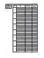
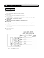
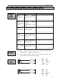
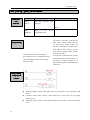
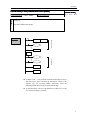
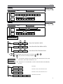
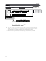
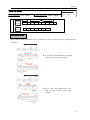
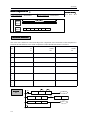
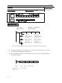
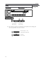
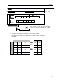
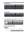
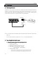
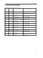
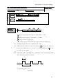
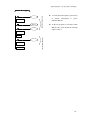
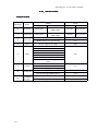
1
XC Series Programmable Controller
User Manual
Xinje Electronic Co., Ltd.
THINGET Xinje Electronic
Preface
Catalog
XC series
————————————————————
Programmable controller
Summary of XC series PLC
�
Operating manual
1
——————————
——————————
Spec.、Input/output and layout
2
————————————————————
Function of each device
————————————————————
Basic SFC instructions
————————————————————
Applied instructions
————————————————————
Special function
————————————————————
Applied examples
4
5
6
————————————————————
7
Appendix
8
————————————————————
V2.5
3
This manual includes some basic precautions which you should follow to keep you safe and protect the
products. These precautions are underlined with warning triangles in the manual. About other manuals that
we do not mention, please follow basic electric operating rules.
Precautions
Correct
Application
Please follow the precautions. If not, it may lead the controlsystem
incorrect or abnormal, even cause fortune lose.
The models could only be used according to the manual, and an only be
used along with the peripheral equipments recognized or recommended
by Xinje Electronic. They could only work normally in the condition of
be transported, kept and installed correctly, also please operate and
maintain them according to the recommendation.
Xinje Electronic Co., Ltd.
Copyright reserved
Without exact paper file allowance, copy, translate or using the manual is not allowed. Disobey this,
people should take the responsibility of loss. We reserve all the right of expansions and their design
patent.
Duty Declare
We have checked the manual, its content fits the hardware and software of the products.As mistakes are
unavoidable, we couldn’t promise all correct. However, we would check the data in the manual frequently,
and in the next edition, we will correct the necessary information. Your recommendation would be highly
appreciated
Preface
Specialties of programmable controller
——Specialties
The programming of XC series programmable controller has the following characteristic:
�
�
�
�
�
�
Support two kinds of program languages
In XC series PLC,besides statement format,you can also adopt ladder chart on the
screen. And, these two formats could convert to the other.
Rich basic functions
Based on the theory o f“Basic functions、High speed dispose、convenient to use”, XC
series PLC can support not only functions relative to sequence control,but also basic
application instructions of data transfer and compare、arithmetic and logic control、loop
and shift of data etc.,besides, it can support interrupt、high-speed counter exclusive
compare instructions 、 high-speed impulse output and other high-speed dispose
instructions.
Offset function (Indirect addressing)
Add offset suffix after the coil、data register (e.g. X3[D100]、 D0[D100]) to realize
indirect addressing. E.g. when D100=0, X3[D100] means X3,D0[D100] means D0;
when D100=9, X3[D100] means X14,D0[D100] means D9;
Single phase or AB high speed counter
The high speed counters in XC series PLC carry on interrupt disposal with the high
speed pulse from special input points. So it is independent with the scan cycle, the
count speed can reach 200KHz.
Convenient MODBUS communication instructions
With Modbus communication instruction, PLC can easily communicate with every kind
of peripheral device as long as they have Modbus protocol.
High speed pulse output
The main units have two routes pulse output, output can be sequencial segments, each
segment of pulse number could be set freely. The pulse could reach 400KHz.
i
XC3
XC5 these three sub-series:
XC series PLC are divided into XC1
XC1、XC3
XC3、XC5
XC1 economic type: This sub-series has specifications of 16 I/O、24 I/O、32 I/O. The function
is simple, suitable for common, small scale applications. They don’t support
high speed count, pulse output, free communication these advanced
functions, also they can not connected with the expansions. For the details,
please refer to the appendix 8-3 “XC1 using description”.
XC3 Standard type: This sub-series belongs to the standard models of XC series PLC. They
could fulfill most using requirements. If no special demonstrate, this manual’s
content are all written for XC3 series PLC.
XC5 strength type: This sub-series has specifications of 32 I/O、48 I/O、60 I/O . Besides the
functions of XC3-PLC, XC5-32 has function of 4 channels pulse output,
XC5-48, XC5-60 support CANBUS instructions, they can realize CAN bus
network function. For the details, please refer to the appendix 8-4 “XC5 using
description”
2
Memo
4
Summary of XC series PLC
1.Summary
XC series PLC are mini type PLC with powerful function. This series products can satisfy diverse control
requirement. With compact design、excellent extend capability、cheap price and powerful function, XC series PLC
has become perfect solution of small size control.
1-1.Summary of XC series PLC and program format
1-2.XC series PLC’s model and type
1-3.Expansion’s constitution and ID assignment
1-4.General specification
1-5.Shape and Size
1-6.Terminal arrangement
1-7.Communication ports’ definition
5
Summary of XC series PLC and program format
1-1
1-1.Summary
6
XC 系列 PLC 的概述
XC series programmable controller
Introduction
�
�
�
�
�
Program
Format
I/O 14~60 points
FlashROM memory inside
Real time clock:With clock inside, Li battery power drop memory
Multi-COM ports, can connect with inverters、instruments、printers etc.
Rich instructions, convenient to program
Statement Program
《Statement
Program》
Statement program is the format which u se“LD”、“AND”、“OUT”etc. these
SFC instructions to input. This format is the basic input form to compile the
SFC program. But it’s not convenient for understanding.
E.g: Step Instruction ID
0
LD
X000
1
OR
Y005
2
ANI
X002
3
OUT
Y005
Ladder Program
《Ladder
Program》
Use sequencial control signal and soft unit’s ID to draw the sequencial
circuit’s graph on the screen, which is called ladder program. As this method
uses trigger point’s symbols and coil symbols to denote the sequencial control
circuit,so it is easy to understand the program’s contents. At the same time
it’s also available to monitor the PLC’s action via the status displayed in the
circuit.
E.g:
X0
X2
Y 5
Y5
Alternation
The programs compiled with the preceding two methods are both stored in
the PLC’s program memory in the format of instruction table. So , the
denotion and edition of this two program format can convert to the other.
7
XC 系列 PLC 的概述
XC series PLC
1-2
1-2.XC
PLC’’s Model and Type
XC3
XC Series
Main Units
1
2
1: Series Name
3
4
5
XC1 series、XC3 series、XC5 series、
2: I/O points
3: Input Format(NPN) R:Relay output
T:Transistor output
RT : Mix output of Transistor /Relay ( Y0 、 Y1 are
transistor)
Output Format(PNP)PR:Relay output
PT:Transistor output
PRT : Mix output of Transistor /Relay ( Y0 、 Y1 are
transistor)
4: Supply Power
E:AC Power(220V)
C:DC Power(24V)
5: Clock
S:With clock and RS485 COM port inside
Vacant:Without clock and RS485 COM port inside
XC1 series models
models:
Model
AC Power
Relay Output
N
DC Power
Transistor
Output
Relay Output
Transistor
Input
Output
DC24V
(DC24V
DC24V)
R,T
T)
(R
Output
XC3-16R-E
XC3-16T-E
XC3-16R-C
XC3-16T-C
8 points
8 points
XC3-24R-E
XC3-24T-E
XC3-24R-C
XC3-24T-C
12 points
12 points
Type
XC3-32R-E
XC3-32T-E
XC3-32R-C
XC3-32T-C
16 points
16 points
P
XC3-16PR-E
XC3-16PT-E
XC3-16PR-C
XC3-16PT-C
8 points
8 points
XC3-24PR-E
XC3-24PT-E
XC3-24PR-C
XC3-24PT-C
12 points
12 points
Type XC3-32PR-E
XC3-32PT-E
XC3-32PR-C
XC3-32PT-C
16 points
16 points
P
N
N
P
8
XC 系列 PLC 的概述
XC3 series models
models:
Model
AC Power
Relay Output
N
P
N
Type
P
N
P
Type
DC Power
Transistor
Mix output
Output
(R&T)
XC3-14R-E
XC3-14T-E
XC3-14RT-E
XC3-24R-E
XC3-24T-E
XC3-32R-E
Relay Output
Input
Output
DC24V
R,T
T)
(DC24V
DC24V) (R
Transistor
Mix output
Output
(R&T)
XC3-14R-C
XC3-14T-C
XC3-14RT-C
8 points
6 points
XC3-24RT-E
XC3-24R-C
XC3-24T-C
XC3-24RT-C
14 points
10 points
XC3-32T-E
XC3-32RT-E
XC3-32R-C
XC3-32T-C
XC3-32RT-C
18 points
14 points
XC3-48R-E
XC3-48T-E
XC3-48RT-E
XC3-48R-C
XC3-48T-C
XC3-48RT-C
28 points
20 points
XC3-60R-E
XC3-60T-E
XC3-60RT-E
XC3-60R-C
XC3-60T-C
XC3-60RT-C
36 points
24 points
XC3-14PR-E
XC3-14PT-E
XC3-14PRT-E
XC3-14PR-C
XC3-14PT-C
XC3-14PRT-C
8 points
6 points
XC3-24PR-E
XC3-24PT-E
XC3-24PRT-E
XC3-24PR-C
XC3-24PT-C
XC3-24PRT-C
14 points
10 points
XC3-32PR-E
XC3-32PT-E
XC3-32PRT-E
XC3-32PR-C
XC3-32PT-C
XC3-32PRT-C
18 points
14 points
XC3-48PR-E
XC3-48PT-E
XC3-48PRT-E
XC3-48PR-C
XC3-48PT-C
XC3-48PRT-C
28 points
20 points
XC3-60PR-E
XC3-60PT-E
XC3-60PRT-E
XC3-60PR-C
XC3-60PT-C
XC3-60PRT-C
36 points
24 points
Input
Output
XC5 series models
models:
Model
AC Power
DC Power
Transistor
Mix output
Output
(R&T)
-
XC5-32T-E
XC5-32RT-E
XC5-48R-E
XC5-48T-E
Type
XC5-60R-E
P
DC24V
R,T
T)
(DC24V
DC24V) (R
Transistor
Mix output
Output
(R&T)
-
XC5-32T-C
XC5-32RT-C
18 points
14 points
XC5-48RT-E
XC5-48R-C
XC5-48T-C
XC5-48RT-C
28 points
20 points
XC5-60T-E
XC5-60RT-E
XC5-60R-C
XC5-60T-C
XC5-60RT-C
36 points
24 points
-
XC5-32PT-E
XC5-32PRT-E
-
XC5-32PT-C
XC5-32PRT-C
18 points
14 points
XC5-48PR-E
XC5-48PT-E
XC5-48PRT-E
XC5-48PR-C
XC5-48PT-C
XC5-48PRT-C
28 points
20 points
Type XC5-60PR-E
XC5-60PT-E
XC5-60PRT-E
XC5-60PR-C
XC5-60PT-C
XC5-60PRT-C
36 points
24 points
Relay Output
N
P
Relay Output
N
N
P
9
XC 系列 PLC 的概述
XC
Switch Quantity
Expansions
E
1
2 3
4
5
6
1、 Series name
2、 E:Expansion
3、 Input points
4、 X:Input
5、 Output points
6、 Output format YR:Relay output YT:Transistor output
Model
10
I/O points
Input
Output
DC24V
(DC24V
DC24V)
R,T
T)
(R
Input
Relay Output
Transistor Output
-
XC-E8YR
XC-E8YT
8 points
-
8 points
XC-E16X
-
-
16 points
16 points
-
-
XC-E16YR
XC-E16YT
16 points
-
16 points
-
XC-E8X8YR
XC-E8X8YT
16 points
8 points
8 points
XC-E16X16YR
XC-E16X16YT
32 points
16 points
16 points
XC-E32X
-
-
32 points
32 points
-
-
XC-E32YR
-
32 points
-
32 points
XC 系列 PLC 的概述
Expansion
1-3
1-3.Expansion
Expansion’’s constitution and ID assignment
XC series PLC can be used independently or used along with the expansions. The
following is the chart of a basic unit with 7 expansions.
Expansion
COM
COM
X0
X1
X2
X3
X4
X5
X6
X7
X10
X11
X12
X13
X14
X15
X16
X17
X20
X21
X22
X23
X24
X25
X26
X27
X30
X31
X32
X33
X34
X35
X36
X37
X40
X41
X42
X43
L
N
FG
COM
X0
X2
X4
X6
X1
X3
X5
X7
0 1 2 3 4 5 6 7
L
N
FG
COM
X0
X2
X4
X6
X1
X3
X5
X7
0 1 2 3
4 5 6 7
X
X
PORT1
XC5-60R-E
PORT2
PWR
RUN
ERR
N
FG
COM
X0
X2
X4
X6
X1
X3
X5
X7
X
PWR
Y
N
FG
COM
X0
X2
X4
X6
X1
X3
X5
X7
X
PWR
Y
N
FG
COM
X0
X2
X4
X6
X1
X3
X5
X7
X
PWR
Y
N
FG
COM
X0
X2
X4
X6
X1
X3
X5
X7
X
PWR
Y
N
FG
COM
X0
X2
X4
X6
X1
X3
X5
X7
0 1 2 3
4 5 6 7
XC-8PT
X
PWR
RUN
ERR
L
0 1 2 3
4 5 6 7
XC3-4AD2DA
RUN
ERR
L
0 1 2 3
4 5 6 7
XC-8AD
RUN
ERR
L
0 1 2 3
4 5 6 7
XC-E8X8YR
RUN
ERR
L
0 1 2 3
4 5 6 7
XC-E16X
RUN
Y
L
0 1 2 3
4 5 6 7
XC-E16YR
XC-6PT-P
X
PWR
RUN
ERR
Y
PWR
RUN
ERR
Y
ERR
Y
0 1 2 3 4 5 6 7
0 1 2 3
4 5 6 7
24V
0V
A
B
CAN+
CAN-
COM0
Y0
COM1
Y1
COM2
Y2
COM3
Y3
Constitution
Rules
Y4
Y5
Y6
COM4
Y7
Y10
Y11
Y12
Y23
Y25
Y27
Y13
Y15
COM6
Y20
Y22
COM5
Y14
Y16
Y17
Y21
COM7
Y24
Y26
�
�
�
0V
24V
B
A
Y0
COM1
Y3
Y5
COM0 Y1
Y2
Y4
0 1 2 3
4 5 6 7
0V
24V
B
A
COM0
Y0
Y1
COM1
Y2
Y3
0 1 2 3
4 5 6 7
Y4
Y5
0V
24V
B
A
Y0
COM0
Y1
COM1
Y2
Y3
0 1 2 3
4 5 6 7
Y4
Y5
0V
24V
B
A
COM0
Y0
Y1
COM1
Y2
Y3
0 1 2 3
4 5 6 7
Y4
Y5
0V
24V
B
A
Y0
COM1
Y3
Y5
COM0 Y1
Y2
Y4
0 1 2 3
4 5 6 7
0V
24V
B
A
Y0
COM1
Y3
Y5
COM0 Y1
Y2
Y4
0 1 2 3
4 5 6 7
0V
24V
B
A
Y0
COM1
Y3
Y5
COM0 Y1
Y2
Y4
Input/Output switch quantity is Octal
Input/Output analog quantity is Decimal
PLC main units can connect with 7 expansions and a BD module. The
input/output type is not limited, both switch or analog quantity are available.
11
XC 系列 PLC 的概述
ID
Unit
As register
ID
ID(As
register)
Input switch quantity X
X100~X137
32 points
Output switch quantity Y
Y100~Y137
32 points
Input analog quantity ID
ID100~ID131
16 channels
Output analog quantity QD
QD100~QD131
16 channels
Module’s set value D
D8250~D8259
-
Input switch quantity X
X200~X237
32 points
Output switch quantity Y
Y200~Y237
32 points
Input analog quantity ID
ID200~ID231
16 channels
Output analog quantity QD
QD200~QD231
16 channels
Module’s set value D
D8260~D8269
-
Input switch quantity X
X300~X337
32 points
Output switch quantity Y
Y300~Y337
32 points
Input analog quantity ID
ID300~ID331
16 channels
Output analog quantity QD
QD300~QD331
16 channels
Module’s set value D
D8270~D8279
-
Input switch quantity X
X400~X437
32 points
Output switch quantity Y
Y400~Y437
32 points
Input analog quantity ID
ID400~ID431
16 channels
Output analog quantity QD
QD400~QD431
16 channels
Module’s set value D
D8280~D8289
-
Input switch quantity X
X500~X537
32 points
Output switch quantity Y
Y500~Y537
32 points
Input analog quantity ID
ID500~ID531
16 channels
Output analog quantity QD
QD500~QD531
16 channels
Module’s set value D
D8290~D8299
-
Input switch quantity X
X600~X637
32 points
Output switch quantity Y
Y600~Y637
32 points
Input analog quantity ID
ID600~ID631
16 channels
Output analog quantity QD
QD600~QD631
16 channels
Module’s set value D
D8300~D8309
-
Input switch quantity X
X700~X737
32 points
Output switch quantity Y
Y700~Y737
32 points
Input analog quantity ID
ID700~ID731
16 channels
Output analog quantity QD
QD700~QD731
16 channels
Module’s set value D
D8310~D8319
-
Input switch quantity X
X1000~X1037
32 points
Output switch quantity Y
Y1000~Y1037
32 points
Input analog quantity ID
ID1000~ID1031
16 channels
Output analog quantity QD
QD1000~QD1031
16 channels
Module’s set value D
D8320~D8329
-
Assignment
Expansion
1#
Expansion
2#
Expansion
3#
Expansion
4#
Expansion
5#
Expansion
6#
Expansion
7#
BD Board
12
Max points/
Type
Channels
XC 系列 PLC 的概述
General Specification
1-4
1-4.General
General Specification
Items
Insulate voltage
Anti-noise
Ambient temperature
Ambient humidity
COM 1
COM 2
COM 3
COM 4
Installation
Grounding
Specifications
Up to DC 500V 2MΩ
1000V 1uS pulse per minute
0℃~60℃
5%~95%
RS-232, connect with host machine、HMI program or debug
RS-232/RS-485, connect with network or aptitude instrument、inverters
etc.
BD board COM port RS-232C/RS-485
CANBUS COM port (XC5 series)
Can use M3 screw to fix or install directly on DIN46277 (Width 35mm)
orbit
The third type grounding (can’t public ground with strong power
system.)
13
XC 系列 PLC 的概述
Performance
XC3 series:
Item
Program executing format
Program format
Dispose speed
Power cut retentive
User program’s capacity
I/O points
Interior coil’s points (M)
Points
Timer(T
)
Spec.
Points
Counter
(C)
Specification
24/32 points
48/60 points
Loop scan format、time scan format
Both statement and ladder
0.5us
Use FlashROM and Li battery
2500 steps
8000 steps
8I/6O
Input 14/18 points
Input 28/36 points
Output 10/14 points Output 20/24 points
8512 points
620 points
100mS timer:Set time 0.1~3276.7 seconds
10mS timer:Set time 0.01~327.67 seconds
1mS timer:Set time 0.001~32.767 seconds
635 points
16 bits counter:set value K0~32767
32 bits counter:set value K0~2147483647
8512 words
2048 words
High speed count、pulse output、external interrupt
0~99mS
6 bits ASCII
Power on self-diagnose、Monitor timer、grammar check
14 points
Spec.
Data Register(D)
FlashROM Register(FD)
High speed dispose function
Setting of time scan space
Password protection
Self diagnose function
Note: If choose “PLC Operation--Secret Download”, “User program’s capacity”
could be larger.
14
XC 系列 PLC 的概述
Shape and Size
1-5
1-5.Shape
Exterior Size
XC1 series 16 points main units
XC3 series 14 points main units (Including 16 points expansions)
63
55
L
N
FG
73.3
COM
X0
X2
X4
X6
X1
X3
X5
X7
110
102
94
XC3-14RT-E
X
PWR
RUN
ERR
Y
0 1 2 3
4 5 6 7
0V
24V
B
A
TYPE:XC3-14R-E
DATE:20060410
SN:0067032266
Xinje Electronic Co.,Ltd
0 1 2 3
4 5 6 7
Y0 COM1 Y3
Y5
COM0 Y1
Y2
Y4
3.5
XC1 series 32 points main units (Including 24 points main units)
32 points expansions)
XC3 series 32 points main units (Including 24 points main units
units、32
XC5 series 32 points main units
139
131
FG
COM
COM
X0
X1
X2
X3
73.3
X4
X5
X6
X7
X10
X11
X13
X12
X14
X15
X17
X16
X20
X21
110
102
94
PORT2
PWR
RUN
ERR
Y
0 1 2 3 4 5
6 7
0V
24V
A
B
COM0
Y0
COM1
Y1
COM2
Y3
Y2
Y4
Y5
COM3
Y6
Y7
Y10
TYPE:XC3-32R-E
DATE:20060410
SN:0067032266
X
XC3-32R-E
PORT1
Xinje Electronic Co.,Ltd
0 1 2 3 4 5
6 7
COM4
Y13
Y15
Y11
Y12
Y14
3.5
15
XC 系列 PLC 的概述
XC3 series 60 points main units (Including 48 points main units)
XC5 series 60 points main units (Including 48 points main units)
207.4
199.4
COM
COM
X0
X1
X2
X3
X4
X5
X6
X7
X10
X11
X12
X13
X14
X15
X16
73.3
X17
X20
X21
X22
X23
X24
X25
X26
X27
X30
X31
X32
X33
X34
X35
X36
X37
X40
X41
X42
X43
XC3-60R-E RUN
ERR
PORT2
Y
0 1 2 3 4 5 6 7
24V
16
0V
CAN+
CANA
B
COM0
Y0
COM1
Y1
COM2
Y2
COM3
Y3
COM4
Y4
COM5
Y5
Y6
Y7
COM6
Y10
Y11
Y12
COM7
Y13
Y14
Y15
Y17
Y16
COM8
Y20
Y21
Y22
Y23
COM9
Y24
Y25
Y26
Y27
TYPE:XC3-60R-E
DATE:20060410
SN:0067032266
PWR
X
PORT1
Xinje Electronic Co.,Ltd
102
94
0 1 2 3 4 5 6 7
XC 系列 PLC 的概述
Terminal arrangement
1-6
1-6.Terminal
Main Units
① Input terminals
② BD expansion
③ Input label
④ COM port
⑤ COM port
⑥ COM port’s cover board
⑦ Output label
⑧Output terminals ⑨ Screws ⑩ Input indicate LED ⑾ Extension port
⑿Programming status indicate LED
⒀ Output indicate LED
XC3- 60 main units、XC5- 60 main units:36 Input/24 Output
XC3- 48 main units、XC5- 48 main units:28 Input /20 Output
COM
0V
24V
CAN+
A
COM
CAN-
X0
B
X1
X2
COM0
X3
Y0
X4
COM1
X5
Y1
X6
COM2
X7
Y2
X10
X11
Y3
COM3
X12
X13
X14
X15
X16
X17
X20
X21
X22
X23
X24
X25
X26
X27
X30
X31
X32
X33
Y4
COM5
Y7
Y10
Y12
COM7
Y15
Y17
Y20
Y22
COM4
Y5
Y11
Y13
Y6
COM6
Y14
Y16
COM8
Y21
Y23
XC1- 32 main units、XC3- 32 main units、XC5- 32 main units:18 Input /14 Output
17
XC 系列 PLC 的概述
FG
0V
A
24V
COM
COM
X1
X0
COM0
B
Y0
X3
X2
COM1
X5
X4
Y3
COM2
Y1
X6
X7
X10
X11
Y5
Y2
Y4
X12
Y6
COM3
X13
Y10
Y7
X14
X15
X16
24V
0V
COM
A
B
COM
X1
X0
COM0
COM1
Y0
X3
X2
Y1
X4
COM2
X5
X6
Y3
Y2
Y4
X7
Y5
XC3- 14 main units:8 Input /6 Output
COM
FG
0V
24V
A
B
X0
X1
X2
X3
X5
X4
X7
X6
Y0 COM1 Y3
Y5
COM0 Y1
Y2
Y4
XC1- 16 main units:8 Input /8 Output
COM
FG
0V
X0
X1
X2
X3
X4
X5
X6
X7
24V
Y0
Y2 COM1
Y5
Y7
Y3
Y4
Y6
COM0 Y1
Expansions
XC-E8X8YR
COM
COM
COM0
Y0
COM1
Y1
X1
X0
COM2
Y2
X2
Y3
X3
X4
COM3
Y4
X5
Y5
X6
Y6
X7
Y7
XC-E16X
COM
COM
COM
X10
COM
X11
X0
X12
X1
X13
X2
X14
X3
X15
X4
X16
X5
X6
X7
X17
XC-E16YR
COM0
COM4
18
Y0
Y10
COM1
COM5
Y1
Y11
COM2
COM6
Y2
Y12
Y3
Y13
COM3
COM7
Y4
Y14
Y5
Y15
Y6
Y16
Y7
Y17
X10
X11
COM3
Y6
X12
Y7
X20
X21
COM4
Y13
Y15
Y11
Y12
Y14
XC1- 24 main units、XC3- 24 main units:14 Input /10 Output
FG
X17
X13
Y10
X14
Y11
X15
XC 系列 PLC 的概述
19
XC 系列 PLC 的概述
COM Port Definition
1-7
1-7.COM
COM 1
Pin of COM 1:
1
2
3 4
6
5
8
7
2:PRG
4:RxD
备注5:TxD
6:VCC
8:GND
Mini Din 88 core socket (hole)
COM 2
Pin of COM 2:
1
2
3 4
6
5
7
4:RxD
5:TxD
8:GND
8
Mini Din 88 core socket (hole)
Program Cable
Connection of programmable cable is the following:
5
2 1
5 43
8
6
7
Mini Din 8 core socket (pin)
20
1
9
6
DB9 pin (hole)
MEMO
14
input/output specification and exterior layout
2.Power circuit
circuit’’s specification
specification、input/output
In this chapter, we’ll tell the power constitution, interior signal circuit’s composing, output circuit’s composing and
exterior layout of XC series PLC.
When using the extend modules or special modules at the same time, please connect the power according to the
user manual.
2-1.Power Specification
2-2.AC Power、DC Input Type
2-3.Input Specification
2-4.DC input signal disposal (AC power type)
2-5.Output Specification
2-6.Disposal of relay output circuit
2-7.Disposal of transistor output circuit
15
电源电路的规格、输入输出规格与外部配线
16
电源电路的规格、输入输出规格与外部配线
Power Specification
2-1
2-1.Power
For the power specification of XC series programmable controller’s basic units, please see the
following table:
AC Power
Type
Rated voltage
AC100V~240V
Voltage allow
bound
Rated frequency
AC90V~265V
Allow momentary
power-cut time
Impact current
Interrupt time≤0.5 AC cycle,alternation≥1 sec
50/60Hz
Max 40A 5mS below/AC100V
below /AC200V
12W
max 60A 5mS
Max power
consumption
Power for sensor 24VDC±10% max 400mA
use
�
�
�
DC power
type
To avoid voltage decrease, please use the power cable thicker than
2mm2
Even appear power cut within 10ms,PLC can still go on working.
But if long time power cut or abnormal power decrease, PLC will
stop working, output will also appear OFF status , when recover
power supply, the PLC will auto start to work.
Connect the grounding terminals of basic units and extend modules
together, then ground
Rated voltage
DC24V
Voltage allow bound
DC21.6V~26.4V
Input current
(Only basic unit)
Allow momentary
power-cut time
Impact current
120mA DC24V
Max power
consumption
Power for sensor use
12W
10mS
DC24V
10A
DC26.4V
24VDC±10% Max 400mA
17
电源电路的规格、输入输出规格与外部配线
2-2
AC Power
DC Input Type
2-2.AC
Power、DC
Constitution
and
Connection
·
�
�
�
�
18
The power is connected between L and N terminals.
24+、COM terminals can be used as power 400mA/DC24V which supply sensor.
·
Besides, this terminal can’t be given power from outside.
terminal is vacant terminal,please don’t go on exterior connection or use it
as relay terminal.
Please connect the basic unit with extend module’s COM
terminal.
电源电路的规格、输入输出规格与外部配线
Input Specification
2-3
2-3.Input
Basic Units
Input signal’s
voltage
DC24V±10%
Input signal’s
current
7mA/DC24V
Input ON current
Up to 4.5mA
Input OFF current
Low than 1.5mA
Input response time
About 10ms
Input signal’s
format
Contact input or
NPN open collector
transistor
Circuit insulation
Photo-electricity
coupling insulation
Input action’s
display
LED light when
input ON
Expansions
Input signal’s
voltage
DC24V±10%
Input signal’s
current
7mA/DC24V
Input ON current
Up to 4.5mA
Input OFF current
Below 1.5mA
Input response time
About 10ms
Input signal’s
format
Contacts input or
NPN open collector
transistor
Circuit insulation
Photo-electricity
coupling insulation
Input action’s
display
LED light
input ON.
when
19
电源电路的规格、输入输出规格与外部配线
DC Input Signal
AC Power Type
2-4
2-4.DC
Signal’’s Disposal
Disposal(AC
Type)
DC input signal
�
�
�
20
Input terminal
When connect input terminal and COM terminal with contacts without voltage or
NPN open collector transistor, if input is ON,LED lamp lights, which indicates input。
There are many COM
terminals to connect in PLC.
Input circuit
Use optical coupling instrument to insulate the input once circuit and twice circuit ,
There’s a C-R filter in the twice circuit 。 It is set to avoid wrong operation caused by
vibration of input contacts or noise along with input signal. As the preceding reason, for
the changing of input ON→OFF,OFF→ON,in PLC, the response time delays about
10ms。There’s a digital filter inside X000~X015。This kind of filter can very from 0~15ms
according to the special register (D8020).
Input sensitive
The PLC’s input current is DC24V 7mA,but to be safe,it needs current up to 3.5mA
when it’s ON,lower than 1.5mA when it’s OFF.
电源电路的规格、输入输出规格与外部配线
Exterior
circuit used
XC series PLC’s input power is supplied by its interior 24V power,so if
use exterior power to drive photoelectricity sensor etc., , this exterior
power should be DC24V±4V,please use NPN open collector type for
sensor’s output transistor
by sensors
Input Connection
21
电源电路的规格、输入输出规格与外部配线
Output Specification
2-5
2-5.Output
Relay output
Interior power
Below AC250V、DC30V
Circuit insulation
Mechanism insulation
Action denote
LED indicate lamp
Max
load
Resistant
load
3A
Induce load
80VA
Lamp load
100W
Open circuit’s leak
current
-
Mini load
DC5V 2mA
Response
time
OFF→ON
10ms
ON→OFF
10ms
Transistor Output
Interior power
Below DC5~30V
Circuit insulation
Optical coupling
insulation
Action denote
Indicate lamp LED
Max
load
Restance
load
0.8A
Induce load
12W/DC24V
Lamp load
1.5W/DC24V
Open circuit’s
current
leak
Mini load
Response
time
22
DC5V 2mA
OFF→ON
Below 0.2ms
ON→OFF
Below 0.2ms
电源电路的规格、输入输出规格与外部配线
Disposal of Relay Output Circuit
2-6
2-6.Disposal
Relay output circuit
�
�
�
�
�
�
�
Output terminals
Relay output type includes 2~4 public terminals. So each public-end unit can drive different powervoltage system’s (E.g.:AC200V,AC100V,DC24V etc.) load.
Circuit
Circuit’’s insulation
Between the relay output coils and contacts,PLC’s interior circuits and exterior circuits, load
circuits are electric insulation. Besides, each public-end blocks are separate.
Action display
LED lamp lights when output relay’s coils galvanize, output contacts are ON.
Response time
From the output relay galvanize (or cut) to the output contacts be ON (or OFF), the response time is
about 10ms
Output current
The current-voltage below AC250V can drive the load of pure resistace 2A/1 point、inductance load
below 80VA(AC100V or AC200V) and lamp load below 100W(AC100V or AC200V).
Open circuit
circuit’’s leak current
When the output contact be OFF and there’s no leak current,can directly drive Ne lamp etc.
The life of relay output contacts
Standard life of induce AC load such as contactor、electromagnetism valve :5 million times for
20VA load. Cut power device’s life according to the company’s test: for 80VA load, the action life is
up to 2 million times. But if the load parallel connect with surge absorber, the life will be greatly
improved!
Output connection example
23
电源电路的规格、输入输出规格与外部配线
Constitution
�
of output
circuit
�
DC load
AC load
24
For DC induce load, please parallel connect with commutate diode.
If not connect with the commutate diode, the contact’s life will be
decreased greatly. Please choose the commutate diode which allow
inverse voltage endurance up to 5~10 times of the load’s voltage,
ordinal current exceeds load current.
Parallel connect AC induce load with surge absorber can reduce
noise.
电源电路的规格、输入输出规格与外部配线
Disposal of Transistor Output Circuit
2-7
2-7.Disposal
Transistor output circuit
�
�
�
�
�
�
�
�
Output terminal
Basic unit’s transistor output has 1~4 public-end output.
Exterior power
Please use DC5~30V steady-voltage power for load drive,
Circuit insulation
Use photoelectricity coupling device to insulate PLC’s interior circuit and output
transistor. Besides, each public block is separate.
Action denote
When drive optical coupling,LED lights,output transistor is ON.
Response time
From photoelectricity coupling device drive (or cut) to transistor ON (or OFF), the time
PLC uses is below 0.2ms.
Output current
The current is 0.5A per point。But as restrict by temperature goes up, the current is 0.8A
every four points.
Open circuit’s current
Below 0.1mA
25
电源电路的规格、输入输出规格与外部配线
E.g. :The following is the connection graph of –RT type PLC with step motor driver。
PLC side
Step motor driver
side
Y0
Y1
26
PU
PU
电源电路的规格、输入输出规格与外部配线
MEMO
27
3.Each Soft Unit
Unit’’s Usage and Function
This chapter, we’ll give some description of the PLC’s data and the function of interior input/output relay, auxiliary
relay, status, counter, data register etc. This item is the base to use PLC.
3-1.Every Soft Unit of PLC
3-2.Soft Unit’s ID List
3-3.Disposal of Data
3-4.Some Encode Principle of Soft Units
3-5.Timer’s ID and Function [T]
3-6.Counter’s ID and Function [C]
3-7.Note Items
29
各种软元件的作用和功能
Every Soft Unit of Programmable Controller
3-1
3-1.Every
In the programmable controller, there are many relays、timers and counters,they all have
countless “a” contacts(Normally open contacts)and “b” contacts(Normally closed contacts),
Connect these contacts and coils to constitute sequencial control circuit. The following, we’ll
briefly introduce each soft unit:
Input
X)and
and output
Y)relay
relay
【Input
Input(X
output(Y
relay】
� In each basic unit , assign the ID of input relay, output relay in the format of
X000~X007,X010~X017…,Y000~Y007,Y010~Y017… this octal format. The ID of
extension is connected behind basic unit.
� The ID of expansion obeys the principle of channel 1 starts from X100/Y100, channel 2
starts from X200/Y200… 7 expansions could be connected totally.
� Use digital filter in the special input filter of input relay, so you can use the program to
change the sieve value. So in the high-speed receive application, you can assign this type
of relay’s ID No.
Auxiliary relay
M)】
【Auxiliary
relay(M
� Auxiliary relay is the relay inside the programmable controller,this type of output relay
is different from input/output relay,it can’t gain exterior input,it also can’t drive exterior
load,it can only be used in the program。
� The relay used for retentive can still save its ON/OFF status in the case of PLC power cut.
Status
S)】
【Status
Status(S
� Relay used as step ladder chart.
� When not used as working procedure No.,it’s the same with auxiliary relay and can be
used as common contact/coil to carry on programming. Besides, it can also be signal
alarm to diagnose exterior trouble.
Timer
T)】
【Timer
Timer(T
� Timer could carry on plus operation to 1ms,10ms,100ms etc. time pulse in PLC, When
reach certain set value, output contact act.
� T100~T199 are timers with the unit of 100ms clock pulse,their current values are the
accumulate values. So, even though timer coil’s drive input is cut, they will still hold the
current value, go on accumulating the action.
30
各种软元件的作用和功能
Counter
C)】
【Counter
Counter(C
� The counters can be divided into the following sorts according the their usage and
purpose:
[Used for interior count] Common use / power failure retentive use
16 bits counter:Used for plus count,count bound: 1~32,767
32 bits counter : Used for add / minus count , count bound: -2,147,483,648~+2 ,
147,483,647
These counters are used for PLC’s interior signals, usually their response speed is below
10Hz.
[Used for high-speed count] For power failure retentive use
32 bits counter: For plus / minus count, count bound: -2,147,483,648~+2,147,483,6487
(Single phase plus count , single phase plus/minus count , AB phase
count) allocate to the special input points.
High-speed counter can count with the frequency below 200kHz , independent with the
PLC’s scan cycle.
Data register
D)】
【Data
register(D
� Data register is the soft unit used by data register to save data. XC series PLC’s data
registers are all 16 bits (The high bit is the sign bit), Combine two registers can carry on
32 bits data disposal (The high bit is the sign bit).
Just the same with other soft units, data registers can also be divided to be two types: for
common use and power failure retentive use.
Constant
K)、(H)
(H)
【Constant
Constant(K
(H)】
� In the diverse value used by PLC, K means decimal integer,H means Hex. Value. They
are used to be the set value and current value for the timer and counter, or applied
instructions’ operands.
Pointer
P)( I)】
【Pointer
Pointer(P
� Pointers are used for branch and interrupt. The pointer (P) used by branch is the jump
aim used for condition jump or subroutine jump. Pointer used for interrupt is used for the
assigned input interrupt, time interrupt.
31
各种软元件的作用和功能
Device
3-2
3-2.Device
Device’’s ID List
For the allocate of device’s ID, please see the following list:
Besides, when connect input / output expansions and special expansions on the basic units, for
the input / output relay’s No., please refer to the user manual.
Bound
Mnemonic
Name
X
Y
M
S
14 points
24\32 points
48 \60 points
Input relay
X000~X007
X000~X015
X000~X021
X000~X033
X000~X043
8 points
14\18 28\36
points points
Output relay
Y000~Y005
Y000~Y011
Y000~Y015
Y000~Y023
Y000~Y027
6 points
10\14 20\24
points points
Flow
Timer
C
Counter
FD
32
M0~M2999【M3000~M7999】
8000
M8000~M8511 for special using
512
S0~S511
【S512~S1023】
1024
Interior relay
T
D
points
14
24\32 48 \60
points points points
T0~T99:100ms not accumulation
T100~T199:100ms accumulation
T200~T299:10ms not accumulation
T300~T399:10ms accumulation
T400~T499:1ms not accumulation
T500~T599:1ms accumulation
T600~T618:1ms with interruption precise time
C0~C299:16 bits forth counter
C300~C598:32 bits forth/back counter
C600~C634:high-speed counter
D0~D3999
【D4000~D7999】
620
635
8000
Data Register
For special usage D8000~D8511
512
FD0~FD1535
1536
For special usage FD8000~FD8511
512
FlashROM
Register
各种软元件的作用和功能
� NOTE
NOTE:
※1. The memorizer area in【 】 is the defaulted power failure retentive area;soft elements
D、M、S、T、C can be set to change the power failure retentive area. For the details,
please see the following table
※2. FlashROM register needn’t set power failure retentive, its data won’t lose when power is
cut (No battery).
※3. The serial No. of input coil、output relay are octal data, other memorizers’ No. are all
algorism data.
※4. The exterior device which is not connected with I/O can be used ad fast-speed interior
Setting of soft unit
unit’’s power failure saving area:
relay.
Mnemonic
Set area
Function
System’s
defaulted
value
Memory bound
of power drop
D
FD8202
Start denotation of D power
cut save area
4000
D4000~D8000
M
FD8203
Start denotation of M power
cut save area
3000
M3000~M8000
T
FD8204
Start denotation of M power
cut save area
620
Not set
C
FD8205
Start denotation of C power
cut save area
320
C320~C640
S
FD8206
Start denotation of S power
cut save area
512
S512~S1024
33
各种软元件的作用和功能
Data Disposal of Programmable Controller
3-3
3-3.Data
According to different usage and purpose, XC series programmable controllers use 5 types of
count format. For their usage and function, see the following:
DEC
《DEC
DEC》(DEC:DECIMAL NUMBER)
� The set value of timer and counter(K constant)
� The ID of auxiliary relay(M),tim er(T),counter(C),status(S)( Soft unit’s
number)
� Assign the value in the operands and instruction’s action(K constant)
HEX
《HEX
HEX》(HEX:HEXADECIMAL NUMBER)
� The same with DEC data,it is used to assign the value in the operands and
instruction’s action(H constant)
BIN
《BIN
BIN》(BIN:BINARY NUMBER)
� Just as said before,carry on data allocation to timer, counter or data register in
the format of DEC. or Hex., But in the PLC, these data are all be put in the
format of binary data. And, when carry on monitor on the peripherial device,
these soft units will auto switch to be DEC. data as shown in the graph.(they
can also switch to be Hex. Data.).
OCT
《OCT
OCT》(OCT:OCTAL NUMBER)
� The input relay, output relay’s soft units’ ID of XC series PLC are allocate in
the format of OCT data. So, it can go on carry of [1-7,10-17,... 70-77,100107].
BCD code
《BCD
code》(BCD: BINARY CODE DECIMAL)
� BCD is the method which use 4 bits binary to denote decimal 0~9. It’s easy to
despose bit. So, BCD is available to denote digital switch or 7 segments display
control.
Other data
float
《Other
data(float
float)》
� XC series PLC has the function of high precision floating point operation. Use binary
floating point data to execute floating point operation, use decimal floating value to
execute monitor.
34
各种软元件的作用和功能
Some encode principles of device
3-4
3-4.Some
Data register could be used as offset
indirect assignment
1、Data
offset(indirect
assignment)
Format:Dn[Dm]、Xn[Dm] 、Yn[Dm] 、Mn[Dm] etc.
M8 0 0 2
M2
M8 0 0 0
MOV
K0
D0
MOV
K5
D0
MOV
D1 0 [D0]
D1 0 0
Y0[D0]
In the preceding example, when D0=0, then D100=D10, Y0 is ON;
When M2 turns from OFF to be ON, D0=5, then D100=D15, Y5 is ON.
When D10[D0]=D[10+D0], Y0[D0]=Y[0+D0].
Word’s
offset
composed
by bit soft units:DXn[Dm] means DX[n+Dm];
�
� Soft units with offset, the offset could only be denoted with soft device D.
2、 Bit units compose word
Input X 、 output Y 、 middle coil M could compose 16 bits word. E.g. DX0 means
X0~X17compose to be a 16 bits data. DX20 means X20~X37 combines a 16 bits data.
Format:Add a D before bit device
Bit devices combine to be word devices:DX、DY、DM、DS、DT、DC
M0
M1
M8 0 0 0
MOV
K2 1
DY0
MOV
K3
D0
MOV
D X 2[D0]
D1 0
In the preceding example, when M0 turns from OFF to be ON, the value of the word DY0 composed
by Y0~Y17 equals 21,i.e. Y0、Y2、Y4 turns to be ON status.
Before M1 be activate, when D0=0, DX2[D0] means a word composed by X2~X21;
When M1turns from OFF to be ON, D0=3, then DX2[D0] means a word composed by X5~X24
� DXn(the bound of “n” is the exact bound of “X”), choose 16 points from the head to the end,
add 0 if not enough.
� Please note, the word composed by bit device couldn’t carry on bit searching address.
35
各种软元件的作用和功能
3、 Bit of word device
Format:Dn..m
Register could carry on bit searching address, e.g. Dn..m means number “m” bit of Dn data
register(0≤m≤15)。
D0.4
Y0
D5[D1] .4
Y1
In the preceding example, D0.4 means when the No.4 bit of D0 is 1, Y0 set ON;
D5[D1].4 means bit searching address with offset, if D1=5,it says D5[D1] means the number 4
bit of D10.
� The bit of word device with offset is denoted as Dn[Dm]..x
� Please note, to the bit of word device, they couldn’t combined to be word device.
4、 T/C means the difference of register
register’’s word and bit
To T and C register, Tn/Cn means be a bit register or a word register should be
distinguished by the instructions.
T、C could denote the status of timer、counter, or the current value of time、counter, it is
distinguished by the instructions.
X0
M0
T1 1
T1 1
MOV
T1 1
K9 9
D0
Y1
In the preceding example,MOV T11 D0,T11 means word register;
LD T11,T11 means bit register.
P,II
5、 Tag type
type:P
e.g.:P means the tag which using CJ instruction or CALL instruction which could jump; I
means interrupt tag.
36
各种软元件的作用和功能
Timer
3-5
3-5.Timer
Timer’’s Number and Function [T]
Timer
Timer’’s number
Please see the following table for the timer’s [T] number (the number
is assigned according to Hex.)
100ms not accumulated(16 bits)
T0~T99
100ms accumulated(16 bits)
T100~T199
10ms not accumulated(16 bits)
T200~T299
10ms accumulated(16 bits)
T300~T399
1ms not accumulated(16 bits)
T400~T499
1ms accumulated(16 bits)
T500~T599
Function
The timer accumulates clock pulse of 1ms,10ms,10ms inside PLC. When
reach the set value, the output contact activates.
The common timers don’t set exclusive instructions, use OUT instruction
to time; use constant K in the program memory, also you could use
register’s content (D) to indirect assign.
Common format
If drive input X000 of time coil T200
is ON, T200 accumulates 10ms clock
pulse with the current value timer. If
this current value equals the set value
K200, timer’s output contact activates.
That is, output contact activates after 2
seconds of coil driving. Driving input
X000 cut or power cut, timer reset,
output contact reset.
Accumulation format
If the drive input X001 of timer’s coil
T300 is ON, T300 accumulates 10ms
clock pulse with the current value
counter. When the value reaches the set
value K2000, counter’s output contact
activates. In the count process, even the
input X001 cut or drop power, when start
again, go on counting, its accumulation
time is 20 seconds. When reset input
X002 is ON, timer reset, output contact
reset.
37
各种软元件的作用和功能
Assign
method of
the set value
《Constant assignment (K)》
T10 is a timer with the unit of
100ms. Assign 100 as a constant,
X0
T1 0
K1 0 0
then 0.1s×100=10s timer work.
《Indirect assignment (D)》
to program or input via data switch.
X0
MOV
Value
K2 0 0
D5
When assigned as power cut retentive
register, please note that voltage low
X1
The Time
Write content in indirect data register
T1 0
D5
will cause the set value instable.
The count format of Timers T0~T599 is 16 bits linear increment mode
(0~K32,767). If the timer’s count value reaches the maximum value K32767,
the timer will stop timing, the timer’s status will remain the same status.
Output delay on-off timer
《Output
timer》
Action
X0
T2
Y0
Y0
X0
T2
X0
K2 0 0
T2
Y0
When X000 is ON, output Y000;
If X000 changes from ON to be OFF, T2(20 seconds)will be delayed, then will
output Y000 cut.
Flicker
《Flicker
Flicker》
X0
T1
T2
T1
K2 0
T2
K1 0
X0
T1
T2
T1
Y0
Y0
If X000 activates, Y000 starts flicker output.
T1 controls the OFF time of Y000, T2 controls the ON time of Y000.
38
各种软元件的作用和功能
Counter
3-6
3-6.Counter
Counter’’s ID and function [C]
For the counter’s number (C), please refer to the following table:
Counter
Counter’’s ID
Counter
Counter’’s
16 bits positive counter
C0~C299
32 bits positive/negative
counter
C300~C598 (C300, C302...C598) (Each one
engrosses 2 counter No.) The number must be
even.
High speed counter
C600~C634(C600,C602...C634) (Each one
engrosses 2 counter No.) The number must be
even
The characters of 16 bits counter and 32 bits counter are shown below:
characters
Items
Count direction
The set value
The assigned set
value
Changing of the
current value
Output contact
Reset activates
The current value
register
16 bits counter
32 bits counter
Positive
Positive/negative
1~32,767
-2,147,483,648~+2,147,483,647
Constant K or data Same as the left, but data register
register
must be in a couple
Change after positive Change after positive count (Loop
count
counter)
Hold the action after Hold the action after positive count,
positive count
reset if negative count
When executing RST command,counter’s current value is 0,
output contacts recover
16 bits
32 bits
39
各种软元件的作用和功能
About the assignment of normally used counter and power failure retentive
counter, they could be changed in the method of changing FD parameters’
setting via the peripheral device.
Function
16 bits counter For normally use or power count retentive
16 bits binary increment counter, its valid setting value is K1~K32,767
(Decimal constant). The set value K0 and K1 have the same meaning, i.e. act
when output contacts at the beginning of first time count.
X0
X1
C0
�
�
�
�
40
RST
C0
C0
K1 0
If cut the PLC’s power, then the value
of the normally use counter will be
reset. However, counter used by power
cut retentive could save the count
value after power cut, and the counter
will go on counting from the value.
Y0
Every time when X001 drives coil C0, the counter’s current value will
increase. When execute the coil instruction the tenth time, output contact
acts. Later, even X001 activates, counter’s current value will not change.
If reset input X000 is ON, execute RST instruction, counter’s current value
is 0, output contacts activates.
For the counter’s set value, it could not only set by constant K, but also be
assigned by data register’s ID. E.g. assign D10, if the content of D10 is
123, it’s the same with setting K123.
When write the set value to the current value register via MOV instruction
etc. When input next time, output coil gets, current value register turns to
the set value.
各种软元件的作用和功能
32 bits counter For normally use or power count retentive
For 32 bits binary increment counter, its valid bound is K1~K2,147,483,647
(Decimal constant). With special auxiliary relay M8238, assign the direction of
bits positive/negative counter’s (C300~C498) direction
�
X2
X3
X4
C3 0 0
�
�
�
Assign
method of
the set value
M8 2 3 8
�
RST
C3 0 0
C3 0 0
K1 0
Y1
If X2 drives M8238, then it is
negative count;If no drive, then it is
positive count.
According to constant K or to the
content of data register D, set the
value to be positive. Treat contents
in consecutive data register as a pair,
and dispose it as 32 bits data. So,
when assign D0, dispose D0 and D1
as a 32 bits set data. If use count
input X004 to drive coil C300,
execute increase count.
When reset input X3 is ON, execute RST instruction, counter’s current
value turns to be 0, output contact resets.
When use counter as power cut retentive, counter’s current value, output
contact’s action and reset status cut power retentive.
32 bits counter can also be used as 32 bits data register. But 32 bits data
register can’t be used as device in 16 bits applied instructions.
� 16 bits counter
器
《Constant assignment(K)》
X0 0 1
C0
K1 0 0
《Indicate assignment(K)》
X0 0 0
X0 0 1
MOV
K1 0 0
C0
D5
D5
41
各种软元件的作用和功能
� 32 bits counter
《Constant assignment(K)》
X0 0 1
C3 0 0
K4 3 ,1 0 0
《Indicate assignment(K)》
X0 0 0
X0 0 1
The count
value
42
DMOV
C3 0 0
K4 3 1 0 0
D0
D0(D1)
The count mode of counters T0~T599 is 16 bits linear increment mode
(0~K32767). When counter’s count value reaches the max value K32767, the
counter will stop counting, the counter’s status will remain.
各种软元件的作用和功能
Some Points to Note
3-7
3-7.Some
Action order of input/output relay and response delay
《Action
delay》
�
Input disposal
Before PLC executing the program, read all the input terminal’s ON/OFF status of PLC to
the image area. In the process of executing the program, even the input changed, the content
in the input image area will not change. However, in the input disposal of next scan cycle,
read out the change.
� Output disposal
Once finish executing all the instructions, transfer the ON/OFF status of output Y image
area to the output lock memory area. This will be the actual output of the PLC. The
contacts used for the PLC’s exterior output will act according to the device’s response
delay time.
When use this input/output format in a batch, the drive time and operation cycle of input
filter and output device will also appear response delay.
Not accept narrow input pulse signal
《Not
signal》
PLC’s input ON/OFF time should be longer than its loop time. If consider input filter’s
response delay 10ms, loop time is 10ms,then ON/OFF time needs 20 ms separately. So, up to
1,000/(20+20)=25Hz input pulse can’t be disposed. But, this condition could be improved
when use PLC’s special function and applied instructions.
Dual output
Dual coils
action
《Dual
output(Dual
coils)action
action》
X1
Y3
X2
Y3
As shown in the left map, please consider
the things of using the same coil Y003 at
many positions:
E.g. X001=ON,X002=OFF
Y4
Y3
At first, X001 is ON, its image area is ON,
output Y004 is also ON.
But, as input X002 is OFF, the image area
of Y003 is OFF.
When executing dual output (use dual coil),
the back side act in prior
So, the actual output is : Y003=OFF,
Y004= ON.
43
各种软元件的作用和功能
44
4.Basic Program Instructions
In this chapter, we tell some basic instructions and their functions.
4-1.List of Basic Instructions
4-2.【 LD】,【LDI】,【OUT】
4-3.【 AND】,【ANI】
4-4.【 OR】,【ORI】
4-5.【 LDP】,【LDF】,【ANDP】,【ANDF】,【ORP】, 【ORF】
4-6.Compare Instructions
4-7.【ORB】
4-8.【ANB】
4-9.【 MCS】,【MCR】
4-10.【ALT】
4-11.【 PLS】, 【PLF】
4-12.【 SET】, 【RST】
4-13.【OUT】, 【RST】 (Compare with counter’s soft unit)
4-14.【 NOP】, 【END】
4-15.Note Items When Programming
45
基本顺控指令说明
46
基本顺控指令说明
List of Basic Instructions
4-1
4-1.List
XC3
XC5 series basic SFC instructions
XC1
XC1、XC3
XC3、XC5
Mnemonic
Function
Format and Device
LD
(LoaD)
Initial logical operation contact
type NO (normally open)
X、Y、M、S、T、C、Dn.m、FDn.m
LDI
(LoaD Inverse)
Initial logical operation contact
type NC (normally closed)
X、Y、M、S、T、C、Dn.m、FDn.m
LDP
(LoaD Pulse)
Initial logical operation-Rising
edge pulse
X、Y、M、S、T、C、Dn.m、FDn.m
LDF
(LoaD Falling Pulse)
Initial logical operation-Falling
/trailing edge pulse
X、Y、M、S、T、C、Dn.m、FDn.m
AND
(AND)
Serial connection of NO
(normally open) contacts
X、Y、M、S、T、C、Dn.m、FDn.m
ANI
(AND Inverse)
Serial connection of NC
(normally closed) contacts
X、Y、M、S、T、C、Dn.m、FDn.m
ANDP
(AND Pulse)
Serial connection of rising edge
pulse
X、Y、M、S、T、C、Dn.m、FDn.m
ANDF
(AND Falling pulse)
Serial connection of
falling/trailing edge pulse
X、Y、M、S、T、C、Dn.m、FDn.m
OR
(OR)
Parallel connection of NO
(normally open) contacts
X、Y、M、S、T、C、Dn.m、FDn.m
ORI
(OR Inverse)
Parallel connection of NC
(normally closed) contacts
X、Y、M、S、T、C、Dn.m、FDn.m
ORP
(OR Pulse)
Parallel connection of rising edge
pulse
X、Y、M、S、T、C、Dn.m、FDn.m
ORF
(OR Falling pulse)
Parallel connection of
falling/trailing edge pulse
X、Y、M、S、T、C、Dn.m、FDn.m
ANB
(ANd Block)
Serial connection of multiply
parallel circuits
None
ORB
(OR Block)
Parallel connection of multiply
parallel circuits
None
OUT
(OUT)
Final logic operation type coil
drive
Y、M、S、T、C、Dn.m
SET
(SET)
Set a bit device permanently ON
Y、M、S、T、C、Dn.m
RST
(ReSeT)
Reset a bit device permanently
OFF
Y、M、S、T、C、Dn.m
PLS
(PuLSe)
Rising edge pulse
X、Y、M、S、T、C、Dn.m
PLF
(PuLse Falling)
Falling/trailing edge pulse
X、Y、M、S、T、C、Dn.m
MCS
Connect the public serial contacts
None
47
基本顺控指令说明
(New bus line start)
MCR
(Bus line return)
Clear the public serial contacts
None
ALT
(Alternate state)
The status of the assigned device
is inverted on every operation of
the instruction
X、Y、M、S、T、C、Dn.m
NOP
(No Operation)
No operation or null step
None
END
(END)
Force the current program scan to
end
None
LDI
OUT
4-2
4-2.【 LD
LD】,,【LDI
LDI】,,【OUT
OUT】
48
基本顺控指令说明
Mnemonic
Mnemonic
Function
LD
Initial logic operation
contact type NO (Normally
Open)
(LoaD)
Format and Devices
M0
Devices:X、Y、M、S、T、C、Dn.m、
FDn.m
LDI
(LoaD Inverse)
Initial logic operation
contact type NC (Normally
Closed)
M0
Devices:X、Y、M、S、T、C、Dn.m、
FDn.m
OUT
(OUT)
Final logic operation type
drive coil
Y0
Devices:X、Y、M、S、T、C、Dn.m、
FDn.m
Statement
�
Connect the LD and LDI instructions directly to the left bus bar. Or use
them to define a new block of program when using ANB instruction.
� OUT instruction is the coil drive instruction for the output relay 、
auxiliary relay、status、timer、counter. For the input relay, cannot use.
� Can not sequentially use parallel OUT command for many times.
� For the timer’s time coil or counter’s count coil, after using OUT
instruction, set constant K is necessary.
� For the constant K’s set bound、actual timer constant、program’s step
relative to OUT instruction(include the set value)
See the following table
Timer/Counter
1ms timer
10ms timer
Setting bound of K
1~32,767
100ms timer
The actual set value
0.001~32.767 seconds
0.01~32.767 seconds
0.1~32.767 seconds
16 bits counter
1~32,767
Same as the left
32 bits counter
1~2,147,483,647
Same as the left
49
基本顺控指令说明
X0
Program
LD
OUT
LDI
OUT
OUT
SP
LD
OUT
Y1 0 0
X1
M1 2 0 3
T 0
T0
K1 9
Y 1
X0
Y100
X1
M1203
T0
K19
T0
Y1
ANI
4-3
4-3.【 AND
AND】,,【ANI
ANI】
Mnemonic
Mnemonic
Function
AND
(AND)
Serial connection of
NO (Normally Open)
contacts
and
Format and Devices
M0
Devices:X、Y、M、S、T、C、Dn.m、
Function
FDn.m
ANI
(ANd Inverse)
Serial connection of
NC (Normally Closed)
contacts
M0
Devices:X、Y、M、S、T、C、Dn.m、
FDn.m
�
Description
�
50
Use the AND and ANI instructions for serial connection of contacts.
As many contacts as required can be connected in series. They can
be used for many times.
The output processing to a coil, through writing the initial OUT
instruction is called a “follow-on” output (For an example see the
program below: OUT M2 and OUT Y003). Follow-on outputs are
permitted repeatedly as long as the output order is correct. There’s no
limit for the serial connected contacts’ No. and follow-on outputs’
number.
基本顺控指令说明
X2 M1
Program
LD
AND
OUT
LD
ANI
OUT
AND
OUT
Y2
Y2 X3
M2
T1
Y3
X2
M1
Y2
Y2
X3
M2
T1
Y3
ORI
4-4
4-4.【 OR
OR】,,【ORI
ORI】
Mnemonic
and
Function
Mnemonic
OR
(OR)
Function
Parallel connection of
NO (Normally Open)
contacts
Format and Devices
M0
Devices:X、Y、M、S、T、C、Dn.m、FDn.m
ORI
(OR Inverse)
Parallel connection of
NC (Normally Closed)
contacts
M0
Devices:X、Y、M、S、T、C、Dn.m、FDn.m
�
Description
�
Use the OR and ORI instructions for parallel connection of contacts.
To connect a block that contains more than one contact connected in
series to another circuit block in parallel, use an ORB instruction.
OR and ORI start from the instruction’s step, parallel connect with the
LD and LDI instruction’s step said before. There is no limit for the
parallel connect times.
51
基本顺控指令说明
X5
Program
X6
Y6
M1 1
Y6 M4 X7
M1 2
M1 3
Relationship
with ANB
52
M1 0 0
LD
OR
OR
OUT
LDI
AND
OR
ANI
OR
OUT
X5
X6
M11
Y6
Y6
M4
M12
X7
M13
M100
The parallel connection with
OR, ORI instructions should
connect with LD, LDI
instructions in principle. But
after the ANB instruction,
it’s available to add a LD or
LDI instruction.
基本顺控指令说明
LDF
ANDP
ANDF
ORP
ORF
4-5
4-5.【 LDP
LDP】,,【LDF
LDF】,,【ANDP
ANDP】,,【ANDF
ANDF】,,【ORP
ORP】,,【ORF
ORF】
Mnemonic
and
Function
Mnemonic
LDP
(LoaD Pulse)
Function
Initial
logical
operation-Rising edge
pulse
Format and Devices
M0
Devices:X、Y、M、S、T、C、Dn.m、FDn.m
LDF
(LoaD Falling
pulse)
ANDP
(AND Pulse)
Initial
logical
operation
Falling/trailing edge
pulse
M0
Devices:X、Y、M、S、T、C、Dn.m、FDn.m
Serial connection of
Rising edge pulse
M0
Devices:X、Y、M、S、T、C、Dn.m、FDn.m
ANDF
(AND Falling
pulse)
Serial connection of
Falling/trailing edge
pulse
M0
Devices:X、Y、M、S、T、C、Dn.m、FDn.m
ORP
(OR Pulse)
Parallel connection of
Rising edge pulse
M0
Devices:X、Y、M、S、T、C、Dn.m、FDn.m
ORF
(OR Falling
pulse)
�
Description
�
M0
Devices:X、Y、M、S、T、C、Dn.m、FDn.m
LDP 、 ANDP 、 ORP are active for one program scan after the
associated devices switch from OFF to ON.
LDF 、 ANDF 、 ORF are active for one program scan after the
associated devices switch from ON to OFF.
X5
X6
Program
Parallel connection of
Falling/trailing edge
pulse
M8 0 0 0 X7
X5
X6
M8 0 0 0 X7
M1 3
M1 5
M1 3
M1 5
LDP
ORP
OUT
LD
ANDP
OUT
X5
X6
M13
M8000
X7
M15
LDF
ORF
OUT
LD
ANDF
OUT
X5
X6
M13
M8000
X7
M15
53
基本顺控指令说明
In the preceding chart, when X005~X007 turns from ON to OFF or
from OFF to ON, M13 or M15 has only one scan cycle activates.
X0
Output drive
M2 0
X0
PL S
M2 0
In two conditions, when X0 turns from OFF to ON, M20 gets a scan cycle.
NOTE
NOTE:
X1 0
X1 0
54
MOV
K1 0
D0
MOV
K1 0
D0
When X10 turns from OFF to ON,
only execute once MOV instruction.
When X10 turns from OFF to ON,
each scan cycle execute once MOV
instruction.
基本顺控指令说明
ORB
4-7
4-7.【ORB
ORB】
Mnemonic
and
Function
Mnemonic
Function
ORB
(OR Block)
Parallel connection of
multiply parallel circuits
Format and Devices
Devices:none
�
Description
�
�
�
To declare the starting point of the circuit (usually serial circuit blocks)
to the preceding circuit in parallel. Serial circuit blocks are those in
which more than one contacts in series or the ANB instruction is used.
An ORB instruction is an independent instruction and is not associated
with any device number.
There are no limitations to the number of parallel circuits when using an
ORB instruction in the sequential processing configuration.
When using ORB instructions in a batch, use no more than 8 LD and LDI
instructions in the definition of the program blocks (to be connected
parallel).
Program
Recommended sequencial
programming method:
LD
AND
LD
AND
ORB
LDI
AND
ORB
OUT
X0
X1
X2
X3
X4
X5
Y10
Non-preferred batch
programming
method:
LD
AND
LD
AND
LDI
AND
ORB
ORB
OUT
X0
X1
X2
X3
X4
X5
Y10
55
基本顺控指令说明
ANB
4-8
4-8.【ANB
ANB】
Mnemonic
Mnemonic
ANB
(ANd Block)
Function
Format and Devices
Serial
connection
of
multiply parallel circuits
and
Devices:none
Function
�
Description
�
To declare the starting point of the circuit block, use a LD or LDI
instruction. After completing the parallel circuit block, connect it to the
preceding block in series using the ANB instruction.
It is possible to use as many ANB instructions as necessary to connect a
number of parallel circuit blocks to the preceding block in series. When
using ANB instructions in a batch, use no more than 8 LD and LDI
instructions in the definition of the program blocks (to be connected in
parallel)
Program
LD
OR
LD
AND
LDI
AND
ORB
OR
ANB
OR
OUT
56
X0
X1
X2
X3
X4
X5
X6
X7
Y20
Start of a branch
Start of a branch
End of a parallel circuit block
End of a parallel circuit block
Serial connect with the preceding circuit
基本顺控指令说明
57
基本顺控指令说明
MCR
4-9
4-9.【 MCS
MCS】,,【MCR
MCR】
Function
Mnemonic
Mnemonic
MCS
(Master control)
Denotes the start
of a master control
block
and
Function
Format and Devices
Y0
Devices:None
MCR
(Master control
Reset)
Denotes the end of
a master control
block
Y0
Devices:None
�
Description
�
�
�
After the execution of an MCS instruction, the bus lin e(LD、LDI)shifts
to a point after the MCS instruction. An MCR instruction returns this to
the original bus line.
MCS、MCR instructions should use in pair.
The bus line could be used nesting. Between the matched MCS、MCR
instructions use matched MCS 、 MCR instructions. The nest level
increase with the using of MCS instruction. The max nest level is 10.
When executing MCR instruction, go back to the upper bus line.
When use flow program, bus line management could only be used in the
same flow. When end some flow, it must go back to the main bus line.
X1
Description
LD
X2
M1
M3
M2
Y0
MCS
Y1
LD
Y2
X1
Bus line starts
X2
OUT
Y0
LD
M1
MCS
Bus line nest
LD
M3
OUT
Y1
LD
M2
OUT
Y2
MCR
MCR
58
Bus line back
基本顺控指令说明
ALT
4-10
4-10.【ALT
ALT】
Mnemonic
and
Function
Mnemonic
ALT
(Alternate
status)
Function
Format and Devices
The status of the assigned
devices inverted on every
operation of the instruction
ALT
M0
Devices: Y、M、S、T、C、Dn.m
Description
The status of the destination device is alternated on every operation of the
ALT instruction.
M1 0 0
Program
M0
M0
ALT
M0
Y0
Y1
LDP
ALT
LD
OUT
LDI
OUT
M100
M0
M0
Y0
M0
Y1
59
基本顺控指令说明
PLF
4-11
4-11.【 PLS
PLS】,,【PLF
PLF】
Mnemonic
and
Function
Mnemonic
PLS
(PuLSe)
Function
Format and Devices
Rising edge pulse
PL S
Y0
Devices: Y、M、S、T、C、Dn.m
PLF
(PuLse
Falling)
�
�
X0
M0
X1
M1
60
PL F
Y0
Devices: Y、M、S、T、C、Dn.m
When a PLS instruction is executed, object devices Y and M operate
for one operation cycle after the drive input signal has turned ON.
When a PLF instruction is executed, object devices Y and M operate
for one operation cycle after the drive input signal has turned OFF.
Description
Program
Falling/trailing edge pulse
PLS
M0
SET
Y0
PLF
M1
RST
Y0
LD
X0
PLS
M0
LD
M0
SET
Y0
---------------------LD
X1
PLF
M1
LD
M1
RST
Y0
基本顺控指令说明
RST
4-12
4-12.【 SET
SET】,,【RST
RST】
Mnemonic
and
Function
Mnemonic
SET
(SET)
Function
Format and Devices
Set a bit device permanently
ON
SE T
Y0
Devices: Y、M、S、T、C、Dn.m
RST
(ReSeT)
Reset
a
bit
permanently OFF
device
RST
Y0
Devices: Y、M、S、T、C、Dn.m
�
Turning ON X010 causes Y000 to turn ON. Y000 remains ON even
after X010 turns OFF. Turning ON X011 causes Y000 to turn OFF.
Y000 remains OFF even after X011 turns OFF. It’s the same with M、S.
SET and RST instructions can be used for the same device as many
times as necessary. However, the last instruction activated determines
the current status.
After assign the start definition ID and end definition ID, operate the
operands in one bound at the same time is available.
Besides, it’s also possible to use RST instruction to reset the current
contents of timer, counter and contacts.
When use SET、 RST instruction, please try to avoid using the same
definition ID with OUT instruction.
Description
�
�
�
�
X1 0
Program
X1 1
X1 2
X1 3
X1 4
X1 5
SET
Y0
RST
Y0
SET
M5 0
RST
M5 0
SET
S0
RST
S0
X1 0
X1 7
T2 5 0
RST
T2 5 0
K1 0
LD
SET
LD
RST
LD
SET
LD
RST
LD
SET
LD
RST
LD
OUT
SP
LD
RST
X10
Y0
X11
Y0
X12
M50
X13
M50
X14
S0
X15
S0
X10
T250
K10
X17
T250
X1 0
X1 1
Y0
61
基本顺控指令说明
RST
for the counters
4-13
4-13.【 OUT
OUT】,,【RST
RST】for
Mnemonic
Mnemonic
and
Function
OUT
(OUT)
Function
Format and Devices
Final logic operation type
coil drive
C
K or D
RST
(ReSeT)
X1 0
Programming
X1 1
C0
of interior
Reset
a
bit
permanently OFF
RST
device
C0
C0
K1 0
Y0
counter
Counter used for power cut retentive.
Even when power is cut, hold the current
value and output contact’s action status
and reset status.
RST
C
C0 carries on increase count for the
OFF → ON of X011. When reach the
set value K10, output contact C0
activates. Afterwards, even X011 turns
from OFF to ON, counter’s current
value will not change, output contact
keep on activating.
To clear this, let X010 be the activate
status and reset the output contact. It’s
necessary to assign constant K or
indirect data register’s ID behind OUT
instruction.
Programming
of high speed
counter
�
�
�
62
In the preceding example, when M0 is ON, carry on positive count with OFF→ON
of X0.
Counter’s current value increase, when reach the set value (K or D), the output
contact is reset.
When M1 is ON, counter’s C600 output contact is reset, counter’s current value turns
to be 0.
基本顺控指令说明
END
4-14
4-14.【 NOP
NOP】,,【END
END】
Mnemonic
NOP
(No
Operation)
Function
No operation
or null step
END (END) Force
current
program
to end
�
Description
�
Format and Devices:None
NOP
Devices: None
the
scan
END
Devices: None
When clear the whole program, all the instructions become NOP. If add
NOP instructions between the common instructions, they have no effect
and PLC will keep on working. If add NOP instructions in the program,
then when modify or add programs, the step vary will be decreased. But
the program should have rest quantity.
If replace the program’s instructions with NOP instructions, then the
circuit will be changed, please note this.
OUT→NOP
AND→NOP ANI→NOP
Contacts short circuit
OR→NOP
ORI→NOP
Open circuit
PLC repeatedly carry on input disposal, program
executing and output disposal. If write END
instruction at the end of the program, then the
instructions behind END instruction won’t be
executed. If there’s no END instruction in the
program, the PLC executes the end step and then
repeat executing the program from step 0.
When debug, insert END in each program segment
to check out each program’s action.
Then, after confirm the correction of preceding
block’s action, delete END instruction.
Besides, the first execution of RUN begins with
END instruction.
When executing END instruction, refresh monitor timer. (Check if scan cycle is a long timer. )
63
基本顺控指令说明
Items To Note When Programming
4-15
4-15.Items
Contacts
1、Contacts
Contacts’’ structure and step number
Even in the sequencial control circuit with the same action, it’s also available to simple the
program and save program’s steps according to the contacts’ structure. General program principle is:a)
write the circuit with many serial contacts on the top;b)write the circuit with many parallel contacts in
the left.
Program
2、Program
Program’’s executing sequence
Handle the sequencial control program by【From top to bottom】and【From left to right】
Sequencial control instructions also encode following this flow.
Dual output dual coil
3、Dual
coil’’s activation and the solution
� If carry on coil’s dual output (dual coil) in the sequencial control program, then the backward
action is prior.
� Dual output (dual coil) doesn’t go against the input rule at the program side. But as the preceding
action is very complicate, please modify the program as in the following example.
X0
X3
X2
X4
Y0
X0
X2
X3
X4
X0
X2
X3
X4
Y0
Y0
M0
M0
M1
Y0
M1
There are other methods. E.g. jump instructions or step ladder. However, when use step ladder, if the
main program’s output coil is programmed, then the disposal method is the same with dual coil, please
note this.
64
基本顺控指令说明
Memo
65
基本顺控指令说明
Applied Instructions
5.Applied
In this chapter, we describe applied instruction’s function of XC series PLC.
5-1.Table of Applied Instructions
5-2.Reading Method of Applied Instructions
5-3.Flow Instructions
5-4.Contactors Compare Instructions
5-5.Move and Compare Instructions
5-6.Arithmetic and Logic Operation Instructions
5-7.Loop and Shift Instructions
5-8.Data Convert
5-9.Floating Operation
5-10.Clock Operation
66
特殊功能
67
特殊功能
Applied Instruction List
5-1
5-1.Applied
The applied instructions’ sort and their correspond instructions are listed in the following table:
Common statements of XC1/XC3/XC5:
�
Sort
Program
Flow
Data
Compare
Data
Move
68
Mnemonic
Function
CJ
Condition jump
CALL
Call subroutine
SRET
Subroutine return
STL
Flow start
STLE
Flow end
SET
Open the assigned flow, close the current flow
ST
Open the assigned flow, not close the current
flow
FOR
Start of a FOR-NEXT loop
NEXT
End of a FOR-NEXT loop
FEND
First end
LD=
LD activates if (S1) = (S2)
LD>
LD activates if (S1) > (S2)
LD<
LD activates if (S1) =< (S2)
LD<>
LD activates if(S1)≠(S2)
LD<=
LD activates if(S1)≤(S2)
LD>=
LD activates if(S1)≥(S2)
AND=
AND activates if(S1)=(S2)
AND>
AND activates if(S1)>(S2)
AND<
AND activates if(S1)<(S2)
AND<>
AND activates if(S1)≠(S2)
AND<=
AND activates if(S1)≤(S2)
AND>=
AND activates if(S1)≥(S2)
OR=
OR activates if(S1)=(S2)
OR>
OR activates if(S1)>(S2)
OR<
OR activates if(S1)<(S2)
OR<>
OR activates if(S1)≠(S2)
OR<=
OR activates if(S1)≤(S2)
OR>=
OR activates if(S1)≥(S2)
MOV
Move
BMOV
Block move
FMOV
Fill move
FWRT
FlashROM written
MSET
Zone set
特殊功能
Data
Operation
ZRST
Zone reset
SWAP
The high and low byte of the destinated devices
are exchanged
XCH
Exchange
ADD
Addition
SUB
Subtraction
MUL
Multiplication
DIV
Division
INC
Increment
DEC
Decrement
MEAN
Mean
WAND
Word And
WOR
Word OR
WXOR
Word exclusive OR
CML
Compliment
NEG
Negative
69
特殊功能
Common statements of XC3/XC5
Data Shift
Data
Convert
Float
Point
Operation
Clock
Operation
70
SHL
Arithmetic Shift Left
SHR
Arithmetic Shift Right
LSL
Logic shift left
LSR
Logic shift right
ROL
Rotation shift left
ROR
Rotation shift right
SFTL
Bit shift left
SFTR
Bit shift right
WSFL
Word shift left
WSFR
WTD
Word shift right
Single word integer converts to double word integer
FLT
32 bits integer converts to float point
FLTD
64 bits integer converts to float point
INT
Float point converts to binary
BIN
BCD converts to binary
BCD
Binary converts to BCD
ASC
Hex. converts to ASCII
HEX
ASCII converts to Hex.
DECO
Coding
ENCO
High bit coding
ENCOL
Low bit coding
ECMP
Float compare
EZCP
Float Zone compare
EADD
Float Add
ESUB
Float Subtract
EMUL
Float Multiplication
EDIV
Float division
ESQR
Float Square Root
SIN
Sine
COS
Cosine
TAN
Tangent
TCMP
Time Compare
TZCP
Time Zone Compare
TADD
Time Add
TSUB
Time Subtract
TRD
Read RTC data
TWR
Set RTC data
特殊功能
Reading Method of Applied Instructions
5-2
5-2.Reading
Understanding method of instruction understanding
In this manual, the applied instructions are described in the following manner.
Note:
①
②
③
④
⑤
⑥
⑦
Denote the instruction name
16 bits instruction and 32 bits instruction
Denotes the soft units which can be used as the operation object
Ladder Example
Flag after executing the instruction. Instructions without the direct flag will not display.
Suitable models for the instruction
S· Source operand, its content won’t change after executing the instruction
D· Destinate operand, its content changes with the execution of the instruction
(8) Tell the instruction’s basic action, using way, applied example, extend function, note items etc.
71
特殊功能
72
特殊功能
The related
description
� The assignment of the data
The data register of XC series PLC is a single word (16 bit) data register, single
word data only engross one data register which is assigned by single word
object instruction. The disposal bound is: Dec. –327,68~327,67, Hex.
0000~FFFF.
Single word object instruction
Instruction D(N U M )
D(NUM)
Object data
Double w o rd(32 bit)engrosses two data register, it’s composed by two consecutive data
registers, the first one is assigned by double word object instruction. The dispose
bound is: Dec. -214,748,364,8~214,748,364,7, Hex. 00000000~FFFFFFFF.
Double word object instruction
Instruction D(N U M )
�
D(NUM+1)
Object data
D(NUM)
Object data
The denote way of 32 bits instruction
If an instruction can not only be 16 bits but also be 32 bits, then the denote method for
32 bits instruction is to add a “D” before 16 bits instruction.
E.g:ADD D0 D2 D4 denotes two 16 bits data adds;
DADD D10 D12 D14 denotes two 32 bits data adds
73
特殊功能
Instructions list of 16 bits and correspond 32 bits
bits:
Program
Flow
Data Move
Data
operation
Data Shift
74
16 bits
CJ
CALL
SRET
STL
STLE
SET
ST
FOR
NEXT
FEND
MOV
BMOV
FMOV
FWRT
ZRST
SWAP
XCH
ADD
SUB
MUL
DIV
INC
DEC
MEAN
WAND
WOR
WXOR
CML
NEG
SHL
SHR
LSL
LSR
ROL
ROR
SFTL
SFTR
WSFL
WSFR
32 bits
-
Data convert
DMOV
DFWRT
DXCH
DADD
DSUB
DMUL
DDIV
DINC
DDEC
DMEAN
DWAND
DWOR
DWXOR
DCML
DNEG
DSHL
DSHR
DLSL
DLSR
DROL
DROR
DSFTL
DSFTR
DWSFL
DWSFR
Float
operation
16 bits
32 bits
WTD
-
FLT
DFLT
INT
DINT
BIN
DBIN
BCD
DBCD
ASC
-
HEX
-
DECO
-
ENCO
-
ENCOL
-
-
ECMP
-
EZCP
-
EADD
-
ESUB
-
EMUL
-
EDIV
-
ESQR
-
SIN
-
COS
TAN
Clock
operation
TCMP
-
TZCP
-
TADD
-
TSUB
-
TRD
-
TWR
-
特殊功能
Program Flow Instructions
5-3
5-3.Program
�
Mnemonic
Instruction’s name
CJ
Condition Jump
CALL
Call subroutine
SRET
Subroutine return
STL
Flow start
STLE
Flow end
SET
Open the assigned flow, close the current flow (flow jump)
ST
Open the assigned flow, not close the current flow (Open the
new flow)
FOR
Start of a FOR-NEXT loop
NEXT
End of a FOR-NEXT loop
FEND
First End
75
特殊功能
Condition Jump [CJ]
16 bits instruction:CJ
32 bits instruction:-
Suitable Models
Models:
XC1、XC3、XC5
Suitable Device
Pointer: P
Soft Unit’s Bound: P0~P9999
Function
and Action
As the instructions of executing list, with CJ instructions, the operate cycle and
dual coil can be greatly shorten.
In the following chart, if X000“ON”,then jump from step 1 to the end step of
flag P6. When X000“OFF”, do not execute jump instructions.
X0
CJ
P6
X1
Y0
X2
X3
X4
RST
T2 4 6
T2 4 6
K1 0 0 0
MOV
K3
CJ
P7
D0
P6
X0
X5
Y 0
P7
X6
RST
T2 4 6
� See the upward graph, Y000 turns to be dual coil and output. But
when X000=OFF, X001 activates. When X000=ON, X005 activates.
� CJ can not jump from one STL to another STL.
� If program timer T0~T640 and high speed counter C600~C640 jump
after driving, go on working, output point also activate.
76
特殊功能
Call subroutine [CALL] and Subroutine return [SRET]
16 bits instruction:CALL、SRET
32 bits instruction:-
Suitable Models
Models:
XC1、XC3、XC5
Suitable Device
Pointer: P
Soft Unit’s Bound: P0~P9999
X0
P1 0
Main program
CALL
Function
FEND
P1 0
Subroutine
SRET
END
� If X000“ON”, carry on Jump instruction and jump to step of
flag P10. Here, after executing the subroutine, return to the
original step via executing SRET instruction. After the
following FEND instruction, program with the flag.
� In the subroutine, 9 levels Call instruction is allowed, so to the
all, 10 levels nesting is available.
77
特殊功能
[ST] 、[STL]
[STL]
Flow [SET]
[SET]、[ST]
[STL]、 [STLE]
16 bits instruction:SET、ST、STL、STLE
32 bits instruction:-
Suitable Models
Models:
XC1、XC3、XC5
Suitable Device
Pointer: S
Soft Unit’s Bound: S0~S
SET
S0
SET
S1
ST
S2
Function
STL S0
STLE
STL S1
STLE
STL S2
STLE
�
�
�
�
�
�
�
�
78
STL and STLE should be used in pairs. STL means start of a flow, STLE means end of a
flow.
After executing of SET Sxxx instruction, the flow assigned by these instructions is ON.
After executing RST Sxxx instruction, the assigned flow is OFF.
In flow S0, SET S1 close the current flow S0, open flow S1.
In flow S0, ST S2 open the flow S2, but don’t close flow S0.
When flow turns from ON to be OFF, OFF or reset OUT、PLS、PLF、not accumulate timer
etc. which belongs to the flow.
ST instruction is usually used when a program needs to run more flows at the same time.
In a main program, usually use ST instruction to open a flow.
特殊功能
[FOR] AND [NEXT]
16 bits instruction:FOR、NEXT
32 bits instruction:-
Suitable Device
D·
D·
Word
Device
K/H
DX
DY
D M
DS
TD
CD
Bit
Device
X
Y
M
S
T
C
D n .m
Function
Suitable Models
Models:
XC1、XC3、XC5
D
FD
First execute the instructions between FOR~NEXT instructions for several times
(the loop time is assigned by the source data), then execute the steps after NEXT.
S·
M0
M1
FOR
K5
FOR
K6
IN C
D0
[A]
NEXT
M3
[C]
FOR
K7
IN C
D1
[B]
NEXT
NEXT
� FOR 、 NEXT instructions must be programmed as a pair. Nesting is allowed, and the
nesting level is 8.
� Between FOR/NEXT, LDP、LDF instructions are effective for one time. Every time when
M0 turns from OFF to ON, and M1 turns from OFF to ON, [A] loop is executed 6 times.
� Every time if M0 turns from OFF to ON and M3 is ON, [B] loop is executed 5×7=35
times.
� If there are many loop times, the scan cycle will be prolonged. Monitor timer error may
occur, please note this.
� If NEXT is before FOR, or no NEXT, or NEXT is behind FENG, END, or FOR and
NEXT number is not equal, an error will occur.
� Between FOR~NEXT, CJ nesting is not allowed, also in one STL, FOR~NEXT must be
programmed as a pair.
[FEND] AND [END]
16 bits instruction:FEND、END
32 bits instruction:-
Suitable Models
Models:
XC1、XC3、XC5
79
特殊功能
Suitable Device
None
Function
An FEND instruction indicates the first end of a main program and the start of the
program area to be used for subroutines. Under normal operating circumstances the
FEND instruction performs a similar action to the END instruction, i.e. output
processing, input processing and watchdog timer refresh are all carried out on
execution.
� If program the tag of CALL instruction behind FEND instruction, there must be SRET
instruction. If the interrupt pointer program behind FEND instruction, there must be SRET
instruction.
� After executing CALL instruction and before executing SRET instruction, if execute FEND
instruction; or execute FEND instruction after executing FOR instruction and before executing
NEXT, then an error will occur.
� In the condition of using many FEND instruction, please compile routine or subroutine
between the last FEND instruction and END instruction.
80
特殊功能
Contactor
5-4
5-4.Contactor
Contactor’’s Compare Instructions
Mnemonic & Function
Mnemonic
�
Function
LD=
Initial comparison contact. Active when the comparison (S1)=(S2) is true.
LD>
Initial comparison contact. Active when the comparison (S1)> (S2) is true
LD<
Initial comparison contact. Active when the comparison (S1)< (S2) is true
LD<>
Initial comparison contact. Active when the comparison (S1)≠(S2) is true
LD<=
Initial comparison contact. Active when the comparison (S1)≤(S2) is true
LD>=
Initial comparison contact. Active when the comparison (S1)≥(S2) is true
AND=
Serial comparison contact. Active when the comparison (S1)=(S2)is true.
AND>
Serial comparison contact. Active when the comparison (S1)> (S2) is true.
AND<
Serial comparison contact. Active when the comparison (S1)< (S2) is true.
AND<>
Serial comparison contact. Active when the comparison (S1)≠(S2) is true.
AND<=
Serial comparison contact. Active when the comparison (S1)≤(S2) is true.
AND>=
Serial comparison contact. Active when the comparison (S1)≥(S2) is true.
OR=
Parallel comparison contact. Active when the comparison (S1)=(S2) is true.
OR>
Parallel comparison contact. Active when the comparison (S1)> (S2) is true.
OR<
Parallel comparison contact. Active when the comparison (S1)< (S2) is true.
OR<>
Parallel comparison contact. Active when the comparison (S1)≠(S2) is true.
OR<=
Parallel comparison contact. Active when the comparison (S1)≤(S2) is true.
OR>=
Parallel comparison contact. Active when the comparison (S1)≥(S2) is true.
81
特殊功能
Initial Comparison LD □
16 bits instruction:Refer Below
32 bits instruction:Refer Below
S1·
Suitable Models
Models:
XC1、XC3、XC5
S2·
Word
Device
K/H
DX
DY
D M
DS
TD
Bit
Device
X
Y
M
S
T
C
CD
D
FD
D n .m
�
S
u
i
t
a
Instruction & Function
The value of S1 and S2 are tested according to the comparison of the instruction. If the comparison is
true then the LD contact is active. If the comparison is false then the LD contact is not active.
�
16
bits
�
32
bi
ts
�
Active
condit
ion
LD
=
DLD=
(S1)=(S2)
(S1)≠(S2)
LD
>
DLD>
(S1)>(S2)
(S1)≤(S2)
LD
<
DLD<
(S1)<(S2)
(S1)≥(S2)
LD
<
>
DLD<>
(S1)≠(S2)
(S1)=(S2)
LD
<
=
DLD<=
(S1)≤(S2)
(S1)>(S2)
LD
>
=
DLD>=
(S1)≥(S2)
(S1)<(S2)
Program
X0
M4
82
LD=
S1·
S2·
K1 0 0
C0
LD>
D2 0 0
K-3 0
DLD>
K6 8 8 9 9
C3 0 0
Y0
X0
SET
Y1
M5 0
Inactive
conditi
on
特殊功能
�
Note Items
�
When the source data’s highest bit (16 bits:b15,32 bits:b31) is 1,use
the data as a negative.
The comparison of 32 bits counter (C300~) must use 32 bits instruction.
If assigned as 16 bits instruction, it will lead the program error or
operation error.
Serial Refer Below AND □
16 bits instruction:Refer Below
Word
Device
e
Bit
Device
32 bits instruction:Refer Below
S1·
Suitable Models
Models:
XC1、XC3、XC5
S2·
K/H
DX
DY
D M
DS
TD
X
Y
M
S
T
C
CD
D
FD
D n .m
�
S
u
i
t
a
Instruction & Function
The value of S1 and S2 are tested according to the comparison of the instruction. If the comparison is
true then the LD contact is active. If the comparison is false then the LD contact is not active.
�
16
bits
32
bi
ts
�
Active
condit
ion
�
Inactive
conditi
on
AND
=
DAND=
(S1)=(S2)
(S1)≠(S2)
AND
>
DAND>
(S1)>(S2)
(S1)≤(S2)
AND
<
DAND<
(S1)<(S2)
(S1)≥(S2)
AND
DAND<>
<>
Program DAND<=
AND
<=
(S1)≠(S2)
(S1)=(S2)
(S1)≤(S2)
(S1)>(S2)
AND
>=
(S1)≥(S2)
(S1)<(S2)
DAND>=
83
特殊功能
X0
X1
X2
S1·
S2·
AND=
K1 0 0
C0
AND>
K-3 0
D0
DAND>
K6 8 8 9 9
D1 0
Y0
SET
Y1
M5 0
M4
�
Note Items
�
84
When the source data’s highest bit (16 bits:b15,32 bits:b31) is 1,use
the data as a negative.
The comparison of 32 bits counter (C300~) must use 32 bits instruction.
If assigned as 16 bits instruction, it will lead the program error or
operation error.
特殊功能
Parallel Comparision OR □
16 bits instruction:Refer Below
32 bits instruction:Refer Below
S1·
Suitable Models
Models:
XC1、XC3、XC5
S2·
Word
Device
K/H
DX
DY
D M
DS
TD
Bit
Device
X
Y
M
S
T
C
CD
D
FD
D n .m
�
S
u
i
t
a
Instruction & Function
The value of S1 and S2 are tested according to the instruction. If the comparison is true then the AND
contact is active. If the comparison is false then the AND contact is not active.
16 bits
32 bits
Active condition
Inactive condition
AND=
DAND=
(S1)=(S2)
(S1)≠(S2)
AND>
DAND>
(S1)>(S2)
(S1)≤(S2)
AND<
DAND<
(S1)<(S2)
(S1)≥(S2)
AND<>
DAND<>
(S1)≠(S2)
(S1)=(S2)
AND<=
DAND<=
(S1)≤(S2)
(S1)>(S2)
AND>=
DAND>=
(S1)≥(S2)
(S1)<(S2)
Program
X0
Y0
OR=
X2
�
�
S2·
K1 0 0
C0
M4
DOR>
Note Items
S1·
M5 0
D1 0
K6 8 8 9 9
When the source data’s highest bit (16 bits:b15,32 bits:b31) is 1,use
the data as a negative.
The comparison of 32 bits counter (C300~) must be 32 bits instruction.
If assigned as a 16 bits instruction, it will lead the program error or
operation error.
85
特殊功能
Data Move
5-5
5-5.Data
Mnemonic
Function
MOV
Move
BMOV
Block Move
FMOV
Fill Move
FWRT
Written of FlashROM
MSET
Zone Set
ZRST
Zone Reset
SWAP
Float To Scientific
XCH
Exchange
86
特殊功能
[MOV]
16 bits instruction:MOV
32 bits instruction:DMOV
Suitable Models
Models:
XC1、XC3、XC5
Suitable Device
S·
Word
Device
K/H
Bit
Device
X
DX
DY
D M
DS
TD
CD
D
FD
D·
Y
M
S
T
C
D n .m
Function & Action
X0
MOV
S·
D·
K1 0
D1 0
Move data from one storage area to a new one.
� Move contents from source to destination
� If X000 is OFF, data will not change.
� Constant K10 will automatically convert to be BIN code.
《Read out the current value of timer、counter》
X1
MOV
T0
D2 0
(T0 current value)→(D20)
It’s the same with the counter.
《Indirect assign the set value of timer、counter》
X2
MOV
K1 0
D2 0
(K10)( D10)
M0
T2 0
D20=K10
D2 0
《Move of 32 bits data》
DMOV
D0
D1 0
(D1,D0)→(D11,D10)
DMOV
C2 3 5
D2 0
(C235, current value)→(D21,D20)
87
特殊功能
[BMOV]
16 bits instruction:BMOV
Suitable Models
Models:
XC1、XC3、XC5
32bits instruction:-
Suitable Device
S·
Word
Device
K/H
n
DX
Bit
Device
X
Y
DY
D M
DS
TD
CD
D
FD
D·
M
S
T
C
D n .m
Function
�
A quantity of consecutively occurring data elements can be copied to a new destination. The
source data is identified as a device head address(S) and a quantity of consecutive data elements
(n). This is moved to the destination device (D) for the same number of elements (n). (If the
quantity of source device (n) exceeds the actual number of available source devices, then only
those devices which fall in the available range will be used. If the number of source devices
exceeds the available space at the destination location, then only the available destination devices
will be written to.)
X0
BM OV
�
�
D·
n
D5
D1 0
K3
D5
D1 0
D6
D1 1
D7
D1 2
n=3
The BMOV instruction has a built in automatic feature to prevent overwriting errors from
occurring when the source (S-n) and destination (D-n) data ranges coincide. This is clearly
identified in the following diagram:
(NOTE: The numbered arrows indicate the order in which the BMOV is processed).
D1 0
D1 1
①
②
③
D1 2
D1 0
D1 1
D1 2
88
S·
D9
D1 0
D1 1
③
②
①
D1 1
D1 2
D1 3
特殊功能
[FMOV]
16 bits instruction:FMOV
Suitable Device
�
�
�
32 bits instruction:-
S·
Word
Device
K/H
n
DX
Bit
Device
X
Y
Function
Suitable Models
Models:
XC1、XC3、XC5
DY
D M
DS
TD
CD
D
FD
D·
M
S
T
X0
FM O V
C
D n .m
S·
D·
n
K0
D0
K1 0
Move K0 to D0~D9. Copy a single data device to a range of destination devices.
The data stored in the source device (S) is copied to every device within the destination range, The
range is specified by a device head address (D) and a quantity of consecutive elements (n).
If the specified number of destination devices (n) exceeds the available space at the destination
location, then only the available destination devices will be written to.
K0
K0
D0
K0
D1
K0
D2
K0
D3
K0
D4
n
K0
D5
K0
D6
K0
D7
K0
D8
K0
D9
89
特殊功能
[FWRT]
16 bits instruction:FWRT
32 bits instruction:DFWRT
Suitable Models
Models:
XC1、XC3、XC5
Suitable Device
S·
Word
Device
K/H
Bit
Device
X
DX
DY
D M
DS
TD
CD
D
FD
D·
Y
M
S
T
C
D n .m
Written of a word
1、Written
Function
X0
FW RT
S·
D·
D0
FD 0
Function:write value in D0 into FD0
Written of double word
2、Written
X1
DFW RT
S·
D·
D0
FD 0
Function:write value in D0、D1 into FD0、FD1
Written of multi-word
3、Written
X2
FW RT
S·
D1·
D3·
D0
FD 0
K3
Function:write value in D0、D2、D3 into FD0、FD1、FD2.
Note:1, FWRT instruction only allow to write data into FlashROM register. In this storage area,
even battery drop, data could be stored. So it could be used to store important technical
parameters.
2, Written of FWRT needs a long time, about 150ms, so, frequently operate this operation is
not recommended.
3, The written time of FlashROM is about 1,000,000 times. So, we suggest using edge
signals (LDP、LDF etc.) to trigger.
※ Frequently written of FlashROM will ruin FlashROM forever.
90
特殊功能
[MSET]
16 bits instruction:MSET
Word
Device
K/H
DX
32 bits instruction:-
DY
D M
D1·
Bit
Device
X
Y
Suitable Models
Models:
XC1、XC3、XC5
M
DS
TD
CD
D
FD
D2·
S
T
C
D n .m
�
[ZRST]
S
u
i
t
a
Suitable Models
Models:
XC1、XC3、XC5
16 bits instruction:ZRST
32 bits instruction:D1·
Word
Device
K/H
DX
DY
D M
D1·
Bit
Device
X
Y
M
D2·
DS
TD
CD
D
FD
D2·
S
T
C
D n .m
�
S
u
i
t
a
Function & Action
X0
M SET
X0
ZRST
ZRST
�
D1·
X2
D2·
M1 0
M1 2 0
D1·
D2·
M5 0 0
M5 5 9
D1·
D2·
D0
D1 0 0
Zone Set Unit M10~M120
Zone Reset Bit Unit M500~M559。
Zone Reset Word Unit D0~D100
D2·
Are specified as the same type of soft units, and
When D1· > D2· , only reset the soft unit specified in D1·
D1· < D2·
� As soft unit’s separate reset instruction, RST instruction can be used
to bit unit Y, M, S and word unit T, C, D.
� As fill move for constant K0, 0 can be written into DX, DY, DM, DS,
T, C, D.
Other Reset
Instruction
X1
D1·
Reset M0
RST
M0
RST
T0
Reset the current value and status of T0
RST
D0
Reset the current value and status of C0
FM OV
K0
D0
K1 0 0
Write K0 into D0~D99
91
特殊功能
[SWAP]
16bits instruction:SWAP
Suitable Models
Models:
XC1、XC3、XC5
32 bits instruction:-
Suitable Device
S·
Word
Device
K/H
DX
DY
D M
DS
TD
CD
Bit
Device
X
Y
M
S
T
C
D n .m
D
FD
Function
D1 0
High 8 b its
Low 8 b its
� Low 8 bits and high 8 bits change when it is 16 bits instruction.
� If the instruction is a consecutive executing instruction, each operation cycle should change.
92
特殊功能
[XCH]
16 bits instruction:XCH
32 bits instruction:DXCH
Suitable Device
Word
Device
K/H
DX
DY
Bit
Device
X
Y
M
D1·
D2·
D M
DS
TD
CD
S
T
C
D n .m
D
Suitable Models
Models:
XC1、XC3、XC5
FD
16 bits instruction
《16
instruction》
Function
X0
XCH
Before(D10)=100
D1·
D2·
D1 0
D1 1
→After (D10)=101
(D11)=101
(D11)=100
�
The contents of the two destination devices D1 and D2 are swapped,
�
When drive input X0 is ON, each scan cycle should carry on data exchange,
32 bits instruction
《32
instruction》
please note.
X0
�
DXCH
D1·
D2·
D1 0
D2 0
32 bits instruction [DXCH] swaps value composed by D10、D11 and the value
composed by D20、D21.
93
特殊功能
Data Operation Instructions
5-6
5-6.Data
94
Mnemonic
Function
ADD
Addition
SUB
Subtraction
MUL
Multiplication
DIV
Division
INC
Increment
DEC
Decrement
MEAN
Mean
WAND
Logic Word And
WOR
Logic Word Or
WXOR
Logic Exclusive Or
CML
Compliment
NEG
Negation
特殊功能
Addition Operation [ADD]
16 bits instruction:ADD
Bit
Device
X
DX
DY
D M
S2·
DS
TD
CD
D
FD
D·
X0
Y
M
S
ADD
T
C
Flag
Suitable Device
K/H
Function
32 bits instruction:DADD
S1·
Word
Device
Suitable Models
Models:
XC1、XC3、XC5
Zero
Borrow
Carry
M8020
M8021
M8022
D n .m
S1·
S2·
D·
D1 0
D1 2
D1 4
(D10)+(D12)→(D14)
� The data contained within the two source devices are combined and the total is stored in the
specified destination device. Each data’s highest bit is the sign bit, 0 stands for positive、1
stands for negative. All calculations are algebraic processed.(5+(-8)=-3)
� If the result of a calculation is “0”, the “0” flag acts. If the result exceeds 323,767(16 bits
limit)or 2,147,483,647(32 bits limit), the carry flag acts.(refer to the next page). If the
result exceeds –323,768(16 bits limit)or –2,147,483,648(32 bits limit), the borrow flag
acts(Refer to the next page)
� When carry on 32 bits operation, word device’s low 16 bits are assigned, the device
following closely the preceding device’s ID will be the high bits. To avoid ID repetition, we
recommend you assign device’s ID to be even ID.
� The same device may be used as a source and a destination. If this is the case then the result
changes after every scan cycle. Please note this point.
95
特殊功能
[SUB]
16 bits instruction:SUB
K/H
Bit
Device
X
DX
DY
D M
S2·
DS
TD
CD
D
FD
D·
Y
X0
M
S
SUB
T
C
Flag
Suitable Device
S1·
Word
Device
Function
32 bits instruction:DSUB
Suitable Models
Models::
XC1、XC3、XC5
Zero
Borrow
Carry
D n .m
S1·
S2·
D·
D1 0
D1 2
D1 4
(D10)—(D12)→(D14)
�
appoint the soft unit’s content, subtract the soft unit’s content appointed by S2· in the
format of algebra. The result will be stored in the soft unit appointed by D· . (5-(-8)=13)
� The action of each flag, the appointment method of 32 bits operation’s soft units are both
the same with the preceding ADD instruction.
� The importance is: in the preceding program, if X0 is ON, SUB operation will be
executed every scan cycle
S1·
The relationship of the flag’s action and vale’s positive/negative is shown below:
96
M8020
M8021
M8022
特殊功能
[MUL]
16 bits instruction:MUL
32 bits instruction:DMUL
K/H
Bit
Device
X
DX
DY
D M
S2·
DS
TD
CD
D
FD
D·
Y
M
S
T
C
Flag
S1·
Word
Device
Suitable Models
Models:
XC1、XC3、XC5
Zero
Borrow
Carry
M8020
M8021
M8022
D n .m
�
S
u
i
t
a
Function & action
16 bits operation
《16
operation》
S1·
S2·
D·
D0
D2
D4
X0
MUL
BIN
BIN
×
(D0)
BIN
→
(D2)
16 bits →
16 bits
(D5, D4)
32 bits
� The contents of the two source devices are multiplied together and the result is stored at
the destination device in the format of 32 bits. As in the upward chart: when (D0)=8 、
(D2)=9, (D5, D4) =72.
� The result’s highest bit is the symbol bit: positive (0)、negative (1).
� When be bit unit, it can carry on the bit appointment of K1~K8. When appoint K4, only
the result’s low 16 bits can be obtained.
32 bits operation
《32
operation》
S1·
S2·
D·
D0
D2
D4
X1
DMUL
BIN
(D1,D0) ×
32 bits
BIN
(D3,D2)
32 bits
BIN
→ (D7,D6,D5,D4)
→
64 bits
� In 32 bits operation, when use bit device as the destination address, only low 32 bits
result can be obtained. The high 32 bits result can not be obtained, so please operate
again after transfer one time to the word device
� Even use word device, 64 bits results can’t be monitored at once.
� In this situation, float point data operation is recommended.
97
特殊功能
[DIV]
16 bits instruction:DIV
32 bits instruction:DDIV
K/H
Bit
Device
X
DX
DY
D M
S2·
DS
TD
CD
D
FD
D·
Y
M
S
T
C
Flag
S1·
Word
Device
Suitable Models
Models:
XC1、XC3、XC5
Zero
Borrow
Carry
D n .m
�
S
u
i
t
a
Function & Action
16 bits operation
《16
operation》
S1·
S2·
D·
D0
D2
D4
X0
D IV
Dividend
Divisor
Result
BIN
BIN
BIN
BIN
D4) ┅
(D5)
16 bits
16 bits
(D0)
÷
16 bits
�
(D2)
→
16 bits
Remainder
appoints the device’s content be the dividend, S2· appoints the device’s content be the
divisor, D· appoints the device and the next one to store the result and the remainder.
� In the above example, if input X0 is ON, devision operation is executed every scan cycle.
S1·
32 bits operation
《32
operation》
S1·
S2·
D·
D0
D2
D4
X1
D D IV
Dividend
Divisor
X1
BIN
(D1,D0)
32 bits
D DBIN
IV
÷
(D3,D2)
32 bits
S1·
Result S2·
D0 BIN D2
D·
Remainder
BIN
D4
(D5,D4)┅
(D7,D6)
32 bits
32 bits
� The dividend is composed by the device appointed by S1· and the next one. The
divisor is composed by the device appointed by S2· and the next one. The result and the
remainder are stored in the four sequential devices, the first one is appointed by D·
� If the value of the divisor is 0, then an operation error is executed and the operation of
the DIV instruction is cancelled.
� The highest bit of the result and remainder is the symbol bit (positive:0, negative: 1).
When any of the dividend or the divisor is negative, then the result will be negative.
When the dividend is negative, then the remainder will be negative.
98
M8020
M8021
M8022
特殊功能
[INC] & [DEC]
16 bits instruction:INC、DEC
32 bits instruction:DINC、DDEC
K/H
DX
DY
D M
DS
TD
CD
Bit
Device
X
Y
M
S
T
C
D n .m
D
FD
Flag
D·
Word
Device
Suitable Models:
XC1、XC3、XC5
Zero
Borrow
Carry
M8020
M8021
M8022
�
S
u
i
t
a
Function & Action
Increment [INC
1、Increment
[INC]]
D·
X0
IN C
D0
(D0)+1→(D0)
� On every execution of the instruction the device specified as the destination D· has its
current value incremented (increased) by a value of 1.
� In 16 bits operation, when +32,767 is reached, the next increment will write -32,767 to
the destination device. In this case, there’s no additional flag to identify this change in the
counted value.
Decrement [DEC]
2、Decrement
D·
X1
DEC
D0
(D0)-1→(D0)
� On every execution of the instruction the device specified as the destination D· has its
current value decremented (decreased) by a value of 1.
� When -32,768 or -2,147,483,648 is reached, the next decrement will write +32,767 or
+2,147,483,647 to the destination device.
99
特殊功能
[MEAN]
16 bits instruction:MEAN
Suitable Models
Models:
XC1、XC3、XC5
32 bits instruction:-
K/H
n
DX
Bit
Device
X
Y
DY
D M
DS
TD
CD
D
FD
D·
M
S
T
C
Flag
S·
Word
Device
Zero
Borrow
Carry
D n .m
�
S
u
i
t
a
Function & Action
X0
(D0)
M EAN
+
(D1) + (D2)
3
�
S·
D·
n
D0
D1 0
K3
(D1 0 )
The value of all the devices within the source range is summed and then divided by the
number of devices summed, i.e. n.. This generates an integer mean value which is stored
in the destination device (D) The remainder of the calculated mean is ignored.
� If the value of n is specified outside the stated range (1 to 64) an error is generated.
100
M8020
M8021
M8022
特殊功能
[WAND]
[WAND]、 [WOR] & [WXOR]
16 bits instruction:WAND、WOR
32 bits instruction:DWAND、DWOR
S1·
K/H
Bit
Device
X
DX
DY
D M
S2·
DS
TD
CD
D
Flag
Word
Device
Suitable Models
Models:
XC1、XC3、XC5
FD
D·
Y
M
S
T
C
Zero
Borrow
Carry
M8020
M8021
M8022
D n .m
�
S
u
i
t
a
Function & Action
� Execute logic AND operation with each bit
X0
W AND
S1·
S2·
D·
D1 0
D1 2
D1 4
0&0=0
1&0=0
0&1=0
1&1=1
� Execute logic OR operation with each bit
X0
W OR
S1·
S2·
D·
D1 0
D1 2
D1 4
0 or 0=0 0 or 1=1
1 or 0=1 1 or 1=1
� Execute logic Exclusive OR operation with each bit.
X0
W XOR
S1·
S2·
D·
D1 0
D1 2
D1 4
0 xor 0=0
1 xor 0=1
0 xor 1=1
1 xor 1=0
If use this instruction along with CML instruction, XOR NOT operation could also
be executed.
X0
S1·
S2·
D·
W XOR
D1 0
D1 2
D1 4
CM L
D1 4
D1 4
101
特殊功能
[CML]
16 bits instruction:CML
Suitable Models
Models:
XC1、XC3、XC5
32 bits instruction:DCML
S·
Word
Device
K/H
Bit
Device
X
DX
DY
D M
DS
TD
CD
D
FD
D·
Y
M
S
T
C
D n .m
�
S
u
i
t
a
Function & Action
X0
CM L
S·
D·
D0
DY0
A copy of each data bit within the source device is inverted and then moved to the designated
destination.
�
Each data bit in the source device is inverted (0->1, 1->0) and sent to the destination
device. If use constant K in the source device, it can be auto convert to be binary.
� It’s available when you want to inverted output the PLC’s output
《Reading of inverted input》
X0
X1
X2
X3
X1 7
102
The sequential control instruction in
the left could be denoted by the
following CML instruction.
M0
M1
M2
M3
M1 7
M8 0 0 0
CM L
DX0
D M 0
特殊功能
[NEG]
16 bits instruction:NEG
Suitable Models
Models:
XC1、XC3、XC5
32 bits instruction:DNEG
D·
Word
Device
K/H
DX
DY
D M
DS
TD
CD
Bit
Device
X
Y
M
S
T
C
D n .m
D
FD
�
S
u
i
t
a
Function & Action
D·
X0
NEG
D1 0
(D1 0 ) +1
(D1 0 )
�
The bit format of the selected device is inverted, I.e. any occurrence of a “1’ becomes
a “0” and any occurrence of “0” becomes “1”, when this is complete, a further binary
1 is added to the bit format. The result is the total logic sigh change of the selected
devices contents.
� When using continually executing instructions, then this instruction will be executed
in every scan cycle.
103
特殊功能
Shift Instructions
5-7
5-7.Shift
Mnemonic
104
�
Function
SHL
Arithmetic shift left
SHR
Arithmetic shift right
LSL
Logic shift left
LSR
Logic shift right
ROL
Rotation left
ROR
Rotation right
SFTL
Bit shift left
SFTR
Bit shift right
WSFL
Word shift left
WSFR
Word shift right
特殊功能
[SHL] & [SHR]
16 bits instruction:SHL、SHR
32 bits instruction:DSHL、DSHR
n
Suitable Models
Models:
XC3、XC5
D·
Word
Device
K/H
DX
DY
DM
DS
TD
Bit
Device
X
Y
M
S
T
C
CD
D
FD
D n .m
�
S
u
i
t
a
Arithmetic shift left
《Arithmetic
left》
Function &
� After once execution, the
low bit is filled in 0, the
final bit is stored in carry
flag.
Action
Arithmetic shift right
《Arithmetic
right》
� After once execution, the
high bit is same with the bit
before shifting, the final bit
is stored in carry flag.
Note:
� In the left example, when X1 is ON, left/right shift is executed at every scan cycle.
105
特殊功能
[LSL] & LSR]
16 bits instruction:
32 bits instruction:DLSL、DLSR
n
Suitable Models
Models:
XC3、XC5
D·
Word
Device
K/H
DX
DY
DM
DS
TD
CD
Bit
Device
X
Y
M
S
T
C
D n .m
D
FD
�
S
u
i
t
a
Function & Action
Logic shift left
《Logic
left》
� After once execution, the
low bit is filled in 0, the
final bit is stored in carry
flag.
Logic shift right
《Logic
right》
� After once execution, the
high bit is same with the bit
before shifting, the final bit
is stored in carry flag.
NOTE:
� In every scan cycle, loop shift left/right action will be executed
106
特殊功能
[ROL] & [ROR]
16 bits instruction:ROL、ROR
32 bits instruction:DROL、DROR
n
Suitable Models
Models:
XC3、XC5
D·
Word
Device
K/H
DX
DY
DM
DS
TD
Bit
Device
X
Y
M
S
T
C
CD
D
FD
D n .m
�
S
u
i
t
a
Function & Action
The bit format of the destination device is rotated n bit places to the left on every operation of the
instruction
Rotation shift left
《Rotation
left》
� Every time when X000 turns from OFF
to ON, executes n bits left rotation.
Rotation shift right
《Rotation
right》
� Every time when X000 turns from
OFF to ON, executes n bits right
rotation.
107
特殊功能
[SFTL] & [SFTR]
16 bits instruction:SFTL、SFTR
Word
Device
Bit
Device
32 bits instruction:DSFTL、DSFTR
Suitable Models
Models:
XC3、XC5
n1n2
K/H
DX
DY
DM
X
Y
M
S
DS
TD
CD
D
FD
S·
T
C
D n .m
D·
�
S
u
i
t
a
Function & Action
� The instruction copies n2 source devices to a bit stack of length n1. For every new addition of n2
bits, the existing data within the bit stack is shifted n2 bits to the left/right. Any bit data moving to
the position exceeding the n1 limit is diverted to an overflow area. The bit shifting operation will
occur every time the instruction is processed unless it is modified with either the pulse suffix or a
controlled interlock.
Bit shift left
《Bit
left》
①
M15~M12→Overflow
②
M11~M 8→M15~M 12
③
M 7~M 4→M11~M8
④
M 3~M 0→M7~M4
⑤ X 3~X 0→M3~M0
Bit shift right
《Bit
right》
①
M 3~M 0→Overflow
②
M 7~M 4→M3~M0
③
M11~M 8→M7~M4
④
M15~M12→M11~M8
⑤ X 3~X 0→M15~M12
� In every scan cycle, loop shift left/right action will be executed
108
特殊功能
[WSFL] & [WSFR]
16 bits instruction:WSFL、WSFR
32 bits instruction:DWSFL、DWSFR
n1n2
Word
Device
K/H
Bit
Device
X
Suitable Models
Models:
XC3、XC5
S·
DX
DY
DM
DS
TD
CD
D
FD
D·
Y
M
S
T
C
D n .m
�
S
u
i
t
a
Function & Action
� The instruction copies n2 source devices to a word stack of length n1. For each addition
of n2 words, the existing data within the word stack is shifted n2 words to the left/right.
Any word data moving to a position exceeding the n1 limit is diverted to an overflow area.
The word shifting operation will occur every time the instruction is processed unless it is
modified with either the pulse suffix or a controller interlock.
Word shift left
《Word
left》
①
D25~D22→overflow
②
D21~D18→D25~D22
③
D17~D14→D21~D18
④
D13~D10→D17~D14
⑤ D 3~D 0→D13~D10
n2 字左移
Word shift right
《Word
right》
n2 字右移
①
D13~D10→overflow
②
D17~D14→D13~D10
③
D21~D18→D17~D14
④
D25~D22→D21~D18
⑤ D 3~D 0→D25~D22
� In every scan cycle, loop shift left/right action will be executed
109
特殊功能
Data Convert
5-8
5-8.Data
110
Mnemonic
Function
WTD
Single word integer converts to double word integer
FLT
32 bits integer converts to float point
FLTD
64 bits integer converts to float point
INT
Float point converts to integer
BIN
BCD convert to binary
BCD
Binary converts to BCD
ASC
Hex. converts to ASCII
HEX
ASCII converts to Hex.
DECO
Coding
ENCO
High bit coding
ENCOL
Low bit coding
特殊功能
[WTD]
16 bits instruction:WTD
Suitable Models
Models:
XC3、XC5
32 bits instruction:-
S·
Word
Device
K/H
Bit
Device
X
DX
DY
DM
DS
TD
CD
D
FD
D·
Y
M
S
T
C
D n .m
�
S
u
i
t
a
Function & Action
X0
W TD
S·
D·
D0
D1 0
0 or 1
D1 1
(D0) → (D11,D10)
Single Word Double Word
D0
D1 0
High bits Low bits
� When single word D0 is positive integer, after executing this instruction, the high
bit of double word D10 is 0.
� When single word D0 is negative integer, after executing this instruction, the
high bit of double word D10 is 1.
111
特殊功能
[FLT] & [FLTD]
16 bits instruction:FLT
32 bits instruction:DFLT
S·
Word
Device
K/H
Bit
Device
X
DX
Suitable Models
Models:
XC3、XC5
S·
DY
D M
DS
TD
CD
D
FD
D·
Y
M
S
T
C
D n .m
�
S
u
i
t
a
Function & Action
16 Bits
《16
Bits》
X0
FLT
S·
D·
D1 0
D1 2
(D10)
→
BIN integer
(D13,D12)
Binary float point
32 Bits
《32
Bits》
X0
DFLT
S·
D·
D1 0
D1 2
(D11,D10)→ (D13,D12)
BIN integer
Binary float point
64 Bits
《64
Bits》
X0
FLTD
S·
D·
D1 0
D1 4
(D13,D12,D11,D10)→ (D17,D16,D15,D14)
BIN integer
Binary float point
�
Convert BIN integer to binary float point. As the constant K、H will auto convert by the
float operation instruction, so this FLT instruction can’t be used.
� The instruction is contrary to INT instruction.
[INT]
16 bits instruction:112
32 bits instruction:INT
Suitable Models
Models:
XC3、XC5
特殊功能
S·
Word
Device
K/H
Bit
Device
X
DX
DY
D M
DS
TD
CD
D
FD
D·
Y
M
S
T
C
D n .m
�
S
u
i
t
a
Function & Action
16 位》
《16
X0
(D11,D10)
Binary Floating
IN T
→
S·
D·
D1 0
D2 0
(D20)
BIN integer
Give up the data after the decimal dot
32 位》
《32
X0
(D11,D10)
Binary Floating
D IN T
→
S·
D·
D1 0
D2 0
(D20,D21)
BIN integer
Give up the data after the decimal dot
�
�
�
The binary source number is converted into an BIN integer and stored at the
destination device. Abandon the value behind the decimal point.
This instruction is contrary to FLT instruction.
When the result is 0, the flag bit is ON。
When converting, less than 1 and abandon it, zero flag is ON.
16 bits operation:-32,768~32,767
32 bits operation:-2,147,483,648~2,147,483,647
[BIN]
16 bits instruction:BIN
32 bits instruction:-
Suitable Models
Models:
XC3、XC5
113
特殊功能
S·
Word
Device
K/H
Bit
Device
X
DX
DY
DM
DS
TD
CD
D
FD
D·
Y
M
S
T
C
D n .m
�
S
u
i
t
a
Function & Action
X0
B IN
S·
D·
D1 0
D0
Convert and move instruction of Source (BCD) → destination (BIN)
� When source data is not BCD code, M8067(Operation error), M8068
(Operation error lock) will not work.
� As constant K automatically converts to binary, so it’s not suitable for this
instruction.
[BCD]
16 bits instruction:BCD
114
32 bits instruction:-
Suitable Models
Models:
XC3、XC5
特殊功能
S·
Word
Device
K/H
Bit
Device
X
DX
DY
DM
DS
TD
CD
D
FD
D·
Y
M
S
T
C
D n .m
�
S
u
i
t
a
Function & Action
Convert and move instruction of source (BIN)→destination (BCD).
X0
BCD
S·
D·
D1 0
D0
� This instruction can be used to output data directly to a seven-segment display.
[ASC
[ASCII]
16 bits instruction:ASCI
32 bits instruction:-
Suitable Models
Models:
XC3、XC5
115
特殊功能
S·
Word
Device
K/H
Bit
Device
X
DX
DY
DM
DS
TD
CD
D
FD
D·
Y
M
S
T
C
D n .m
�
S
u
i
t
a
Function & Action
16 bits convert mode
《16
mode》
X0
A SCI
S·
D·
n
D1 0 0
D2 0 0
K4
Convert each bit of source’s (S) Hex. format data to be ASCII code, move separately to the high 8
bits and low 8 bits of destination (D). The convert alphanumeric number is assigned with n.
(D) is low 8 bits, high 8 bits, store ASCII data.
The convert result is the following:
Assign start device:
(D100)=0ABCH
(D101)=1234H
(D102)=5678H
[0]=30H
[A]=41H
[B]=42H
[C]=43H
[1]=31H
[2]=32H
[3]=33H
[4]=34H
[5]=35H
[6]=36H
[7]=37H
[8]=38H
n
D
K1
K2
K3
K4
K5
K6
K7
K8
K9
D200 down
[C]
[B]
[A]
[0]
[4]
[3]
[2]
[1]
[8]
[C]
[B]
[A]
[0]
[4]
[3]
[2]
[1]
[C]
[B]
[A]
[0]
[4]
[3]
[2]
[C]
[B]
[A]
[0]
[4]
[3]
[C]
[B]
[A]
[0]
[4]
[C]
[B]
[A]
[0]
[C]
[B]
[A]
[C]
[B]
D200 up
D201 down
D201 up
D202 down
D202 up
D203 down
D203 up
D204 down
[C]
[HEX]
16 bits instruction:HEX
116
32 bits instruction:-
Suitable Models
Models:
XC3、XC5
特殊功能
S·
Word
Device
K/H
Bit
Device
X
DX
DY
DM
DS
TD
CD
D
FD
D·
Y
M
S
T
C
D n .m
�
S
u
i
t
a
Function & Action
16 bits switch mode
《16
mode》
X0
HEX
S·
D·
n
D2 0 0
D1 0 0
K4
Convert the high and low 8 bits in source to HEX data. Move 4 bits every time to
destination. The convert alphanumeric number is assigned by n.
The convert of the upward program is the following:
(S·)
ASCII
Code
30H
41H
42H
43H
31H
32H
33H
34H
35H
D200 down
D200 up
D201 down
D201 up
D202 down
D202 up
D203 down
D203 up
D204 down
HEX
Convert
0
A
B
C
1
2
3
4
5
(D·)
D102
n
1
2
3
4
5
6
7
8
9
D101
D100
··· 0H
··· 0H
·· 0AH
·0ABH
0ABCH
ABC1H
··· 0H
·· 0AH
·0ABH
0ABCH
ABC1H
BC12H
C123H
1234H
2345H
0
1
0
0
0
0
1
0
1
0
0
Not change to be 0
时
n=k4
D2 0 0
0
1
0
0
0
0
0
1
0
1
4 1 H→[A]
D2 0 1
0
1
0
0
0
3 0 H→[0]
0
1
1
0
1
0
4 3 H→[C]
D2 0 2
0
0
0
0
0
1
0
1
0
4 2 H→[B]
0
1
A
0
1
0
1
B
1
1
C
117
特殊功能
[DECO]
16 bits instruction:DECO
32 bits instruction:-
n
Word
Device
Bit
Device
Suitable Models
Models:
XC3、XC5
S·
K/H
DX
DY
DM
DS
TD
X
Y
M
S
T
C
CD
D
FD
D n .m
D·
�
S
u
i
t
a
Function & Action
《 When
is software unit》 n≤16
D·
S·
X1 0
�
DECO
n
D·
DX0
X0 0 2
0
X0 0 1
1
X0 0 0
1
4
②
①
M1 0
K3
7
0
6
0
5
0
4
0
③
1
2
0
1
0
0
0
M1 7
M1 6
M1 5
M1 4
M1 3
M1 2
M1 1
M1 0
The source address is 1+2=3,so starts from M10, the number 3 bit (M13) is 1. If the source
are all 0, M10 is 1
When n=0, no operation, beyond n=0~16, don’t execute the instruction.
When n=16, if coding command “D” is soft unit, it’s point is 2^8=256。
When drive input is OFF, instructions are not executed, the activate coding output keep on
activate.
�
�
�
《 When
X0
D·
is word device》 n≤4
DECO
S·
D·
n
D0
D1
K3
③
�
�
118
Source ID’s low n bits ( n ≤ 4 ) are encoded to the destination ID. When n ≤ 3,
destination’s high bits all converts to be 0.
When n=0, no disposal, beyond n=0~4, don’t execute the instruction.
特殊功能
[ENCO]
16 bits instruction:ENCO
Word
Device
Bit
Device
Suitable Models
Models:
XC3、XC5
32 bits instruction:S·
K/H
n
DX
X
Y
DY
D M
DS
TD
CD
D
C
D n .m
FD
D·
M
S
T
S·
�
S
u
i
t
a
Function & Action
《 When
S·
is bit device》 n≤16
S·
X0
M1 7
0
7
b1 5
0 0
ENCO
M1 0
M1 6
0
6
M1 5
0
5
M1 4
0
4
M1 3
1
0
D1 0
0 0
0
0
0
0
n
D·
③
0
D1 0
M1 2
0
2
M1 1
1
1
0
0
0
K3
M1 0
0
0
4 ② ①
0 1 1
b0
All be 0
《 When
S·
X1
b1 5
0 1
is word device》 n≤4
ENCO
0
1
D0
0 1
0
1
S·
D·
n
D0
D1
K3
0
0
0
0
1
0
1
b0
0
7
6
5
4 ③
2
1
0
0
0
0
0
4 ② ①
0 1 1
Be ignored
b1 5
0 0
0
0
D1
0 0
0
0
0
b0
All be 0
�
�
�
If many bits in the source ID are 1, ignore the low bits. If source ID are all 0, don’t
execute the instructions.
When drive input is OFF, the instruction is not executed, encode output don’t change.
When n=8, if encode instruction’s “S” is bit unit, it’s point number is 2^8=256
119
特殊功能
[ENCOL]
16 bits instruction:ENCOL
Word
Device
Bit
Device
Suitable Models
Models:
XC3、XC5
32 bits instruction:-
S·
K/H
n
DX
X
Y
DY
D M
DS
TD
CD
D
C
D n .m
FD
D·
M
S
T
S·
�
S
u
i
t
a
Function & Action
《 If
is bit device》 n≤16
S·
S·
X0
M1 7
0
7
b1 5
0 0
ENCOL
M1 0
M1 6
0
6
M1 5
1
5
M1 4
0
4
M1 3
1
0
D1 0
0 0
0
0
0
0
n
D·
③
0
D1 0
M1 2
0
2
M1 1
0
1
0
0
0
K3
M1 0
0
0
4 ② ①
0 1 1
b0
All be 0
《
是字软元件时》 n≤16
S·
X1
b1 5
0 1
ENCOL
0
1
D0
0 1
0
1
Be ignored
b1 5
0 0
0
0
D1
0 0
0
0
S·
D·
n
D0
D1
K3
0
0
1
0
1
0
0
b0
0
7
6
5
4 ③
2
1
0
0
0
0
0
4 ② ①
0 1 1
0
b0
All be 0
�
�
�
120
If many bits in the source ID are 1, ignore the high bits. If source ID are all 0, don’t execute
the instructions.
When drive input is OFF, the instruction is not executed, encode output don’t change.
When n=8, if encode instruction’s “S” is bit unit, it’s point number is 2^8=256
特殊功能
Floating Operation
5-9
5-9.Floating
Mnemonic
Function
ECMP
Float Compare
EZCP
Float Zone Compare
EADD
Float Add
ESUB
Float Subtract
EMUL
Float Multiplication
EDIV
Float Division
ESQR
Float Square Root
SIN
Sine
COS
Cosine
TAN
Tangent
121
特殊功能
[ECMP]
16 bits instruction:-
Word
Device
Bit
Device
32 bits instruction:ECMP
S1·
K/H
DX
X
Y
S2·
DY
D M
DS
M
S
T
S1·
S2·
TD
CD
C
D
Suitable Models
Models:
XC3、XC5
FD
D n .m
D·
�
S
u
i
t
a
Function & Action
(D11,D10) :
Binary Floating
X0
(D21,D20)→M0,M1,M2
Binary Floating
ECM P
M0
M1
S1·
S2·
D·
D1 0
D2 0
M0
(D11, D10)
>
Binary Floating
Binary Floating
(D11, D10)
(D21<D20)
=
Binary Floating
M2
(D21<D20)
(D11, D10)
<
Binary Floating
Binary Floating
(D21<D20)
Binary Floating
The status of the destination device will be kept even if the ECMP instruction is deactivated.
�
The binary float data of S1 is compared to S2. The result is indicated by 3 bit devices
specified with the head address entered as D.
� If a constant K or H used as source data, the value is converted to floating point before
the addition operation.
X0
ECM P
K5 0 0
D1 0 0
(K500) ∶ (D101,D100)→M10,M11,M12
Binary converts
to floating
122
Binary floating
M1 0
特殊功能
[EZCP]
16 bits instruction:-
Word
Device
32 bits instruction:ECMP
K/H
DX
DY
S1·
Bit
Device
Suitable Models
Models:
XC3、XC5
X
Y
D M
S2·
S3·
M
S
S1·
S2·
S3·
DS
TD
CD
T
C
D
FD
D n .m
D·
�
S
u
i
t
a
Function & Action
Compare a float range with a float value.
X0
EZCP
S1·
S2·
D1·
D2·
D1 0
D2 0
D0
M3
(D20, D21)
M3
>
Binary Floating
(D21,D10)
M4
≤
(D1, D0)
ON
Binary Floating
(D1,D0) ≤ (D31,D30)
ON
Binary Floating Binary Floating Binary Floating
(D1, D0)
M5
>
Binary Floating
(D31, D30)
ON
Binary Floating
The status of the destination device will be kept even if the EZCP instruction is deactivated.
�
�
The data of S1 is compared to the data of S2. The result is indicated by 3 bit devices specified with
the head address entered as D.
If a constant K or H used as source data, the value is converted to floating point before the addition
operation.
X0
(K10)
∶
[D6,D5]
EZCP
∶
K1 0
K2 8 0 0
D5
M0
(K2800)→M0,M1,M2
Binary converts Binary Floating
Binary converts
to Floating
to Floating
Please set S1<S2, when S2>S1, see S2 as the same with S1 and compare them.
123
特殊功能
[EADD]
16 bits instruction:-
32 bits instruction:EADD
S1·
Word
Device
K/H
Bit
Device
X
S2·
DX
DY
D M
DS
S2·
S1·
TD
CD
D
Suitable Models
Models:
XC3、XC5
FD
D·
Y
M
S
T
C
D n .m
�
S
u
i
t
a
Function & Action
X0
EAAD
(D11,D10)
+
Binary Floating
S1·
S2·
D·
D1 0
D2 0
D5 0
(D21,D20)
→
Binary Floating
(D51,D50)
Binary Floating
�
The floating point values stored in the source devices S1 and S2 are algebraically added
and the result stored in the destination device D.
� If a constant K or H used as source data, the value is converted to floating point before
the addition operation.
X1
(K1234)
EAAD
+
Binary converts to Floating
D1 0 0
K1 2 3 4
( D101,D100)
Binary Floating
→
D1 1 0
(D111,D110)
Binary Floating
� The same device may be used as a source and as the destination. If this is the case then,
on continuous operation of the EADD instruction, the result of the previous operation
will be used as a new source value and a new result calculated. This will happen every
program scan unless the pulse modifier or an interlock program is used.
124
特殊功能
[ESUB]
16 bits instruction:-
Word
Device
Bit
Device
32 bits instruction:ESUB
S1·
K/H
DX
S2·
DY
D M
S2·
S1·
TD
CD
DS
D
Suitable Models
Models:
XC3、XC5
FD
D·
X
Y
M
S
T
C
D n .m
�
S
u
i
t
a
Function & Action
X0
(D11,D10)
Binary Floating
�
�
ESU B
-
(D21,D20)
S1·
S2·
D·
D1 0
D2 0
D5 0
→
(D51,D50)
Binary Floating
Binary Floating
The floating point value of S2 is subtracted from the floating point value of S1 and the result
stored in destination device D.
If a constant K or H used as source data, the value is converted to floating point before the addition
operation.
X1
ESU B
(K1234)
K1 2 3 4
-
Binary converts to Floating
D1 0 0
(D101,D100)
D1 1 0
→
Binary Floating
(D111,D110)
Binary Floating
� The same device may be used as a source and as the destination. If this is the case then,
on continuous operation of the EADD instruction, the result of the previous operation
will be used as a new source value and a new result calculated. This will happen every
program scan unless the pulse modifier or an interlock program is used.
125
特殊功能
[EMUL]
16 bits instruction:-
32 bits instruction:EMUL
S1·
Word
Device
K/H
Bit
Device
X
DX
S2·
DY
D M
S2·
S1·
TD
CD
DS
D
Suitable Models
Models:
XC3、XC5
FD
D·
Y
M
S
T
C
D n .m
�
S
u
i
t
a
Function & Action
X0
EM UL
S1·
S2·
D·
D1 0
D2 0
D5 0
(D11,D10) × (D21,D20)
Binary Floating
→
Binary Floating
(D51,D50)
Binary Floating
�
The floating value of S1 is multiplied with the floating value point value of S2. The result of
the multiplication is stored at D as a floating value.
� If a constant K or H used as source data, the value is converted to floating point before the
addition operation.
X1
(K100)
EM UL
×
Binary converts to Floating
126
K1 0 0
(D101,D100)
D1 0 0
→
Binary Floating
D1 1 0
(D111,D110)
Binary Floating
特殊功能
[EDIV]
16 bits instruction:-
32 bits instruction:EDDIV
S1·
Word
Device
K/H
Bit
Device
X
DX
S2·
DY
D M
DS
S2·
S1·
TD
CD
D
Suitable Models
Models:
XC3、XC5
FD
D·
Y
M
S
T
C
D n .m
�
S
u
i
t
a
Function & Action
X0
E D IV
S1·
S2·
D·
D1 0
D2 0
D5 0
(D11,D10)÷(D21,D20)→(D51,D50)
Binary Floating Binary Floating Binary Floating
�
�
The floating point value of S1 is divided by the floating point value of S2. The result of the
division is stored in D as a floating point value. No remainder is calculated.
If a constant K or H used as source data, the value is converted to floating point before the addition
operation.
X1
E D IV
(D101,D100)
Binary Floating
÷
D1 0 0
(K100)
K1 0 0
→
Binary converts to Floating
D1 1 0
(D111,D110)
Binary Floating
� If S2 is zero then a divide by zero error occurs and the operation fails.
127
特殊功能
[ESQR]
16 bits instruction:-
32 bits instruction:ESQR
S·
Word
Device
K/H
Bit
Device
X
DX
Suitable Models
Models:
XC3、XC5
S·
DY
D M
DS
TD
CD
D
FD
D·
Y
M
S
T
C
D n .m
�
S
u
i
t
a
Function & Action
X0
E S QR
S·
D·
D1 0
D2 0
(D11,D10) →(D21,D20)
Binary Floating Binary Floating
� A square root is performed on the floating point value in S the result is stored in D.
� If a constant K or H used as source data, the value is converted to floating point before
the addition operation.
X1
(K1024)
E S QR
K1 0 2 4
→
Binary converts to Floating
�
�
128
D1 1 0
(D111,D110)
Binary Floating
When the result is zero, zero flag activates
Only when the source data is positive will the operation be effective. If S is negative then
an error occurs and error flag M8067 is set ON, the instruction can’t be executed.
特殊功能
[SIN]
16 bits instruction:-
32 bits instruction:SIN
S·
Word
Device
K/H
Bit
Device
X
Suitable Models
Models:
XC3、XC5
S·
DX
DY
D M
DS
TD
CD
D
FD
D·
Y
M
S
T
C
D n .m
�
S
u
i
t
a
Function & Action
X0
S IN
(D51,D50)
→
Binary Floating
S·
D·
D5 0
D6 0
(D61,D60)SIN
Binary Floating
� This instruction performs the mathematical SIN operation on the floating
point value in S (angle RAD). The result is stored in D.
S·
D5 1
D5 0
RAD value (angle×π/180)
Assign the binary floating value
D·
D6 1
D6 0
SIN value
Binary Floating
129
特殊功能
[COS]
16 bits instruction:-
32 bits instruction:COS
S·
Word
Device
K/H
Bit
Device
X
Suitable Models
Models:
XC3、XC5
S·
DX
DY
D M
DS
TD
CD
D
FD
D·
Y
M
S
T
C
D n .m
�
S
u
i
t
a
Function & Action
X0
COS
(D51,D50)RAD →
Binary Floating
S·
D·
D5 0
D6 0
(D61,D60)COS
Binary Floating
� This instruction performs the mathematical COS operation on the floating point
value in S (angle RAD). The result is stored in D.
RAD value (angle×π/180)
S·
D5 1
D5 0
D·
D6 1
D6 0
Assign the binary floating value
COS value
Binary Floating
130
特殊功能
[TAN]
16 bits instruction:-
32 bits instruction:TAN
S·
Word
Device
K/H
Bit
Device
X
Suitable Models
Models:
XC3、XC5
S·
DX
DY
D M
DS
TD
CD
D
FD
D·
Y
M
S
T
C
D n .m
�
S
u
i
t
a
Function & Action
X0
TAN
(D51,D50)RAD →
Binary Floating
S·
D·
D5 0
D6 0
(D61,D60)TAN
Binary Floating
� This instruction performs the mathematical TAN operation on the floating
point value in S. The result is stored in D.
S·
D5 1
D5 0
RAD value (angle×π/180)
Assign the binary floating value
D·
D6 1
D6 0
TAN value
Binary Floating
131
特殊功能
Clock Operation
5-10
5-10.Clock
Mnemonic
Function
TCMP
Time Compare
TZCP
Time Zone Compare
TADD
Time Add
TSUB
Time Subtract
TRD
Read RTC data
TWR
Set RTC data
Note:The models without clock can not use these instructions.
132
特殊功能
Time Compare [TCMP]
16 bits instruction:DIV
Word
Device
K/H
32 bits instruction:DDIV
DX
DY
S1·
S2·
S3·
D M
DS
TD
CD
D
Suitable Models
Models:
XC3、XC5
FD
S·
Bit
Device
X
Y
M
S
T
C
D n .m
D·
�
S
u
i
t
a
Function & Action
Compare the assigned time with time data.
The status of the destination devices is kept, even if the TCMP instruction is deactivated.
� 「 S1· , S2· , S3· 」represent hours, minutes and seconds respectively. This
time is compared to the time value in the 3 data devices specified by the head
address S· , The result is indicated in the 3 bit devices specified by the head
address D·
S1·
S2·
S3·
S·
S·
S·
D·
:Assign the compare standard “Hour”
:Assign the compare standard “Minute”
:Assign the compare standard “Second”
:Assign the “Hour” of clock data
+1 :Assign the “Minute” of clock data
+2 :Assign the “Second” of clock data
,D· +1,
D·
+2 :According to the compare result, the 3 devices output ON/OFF.
The valid range of “Hour” is「0~23」.
The valid range of “Minute” is「0~59」.
The valid range of “Second” is「0~59」.
133
特殊功能
[TZCP]
16 bits instruction:DIV
Word
Device
Bit
Device
32 bits instruction:DDIV
S1·
K/H
DX
DY
D M
X
Y
M
S
S2·
DS
TD
CD
T
C
D n .m
Suitable Models
Models:
XC3、XC5
S3·
D
FD
D·
�
S
u
i
t
a
Function & Action
Compare the two assigned time with time data
The status of the destination devices is kept, even if the TCMP instruction is deactivated.
� Compare the 3 clock data start from S· with the two ends on the clock compare bound,
according to the area bound, output the three ON/OFF status starts from D·
即使使用 X000=OFF 停止执行 TZCP 指令时,M0~M2
S1·
S2·
S·
D·
, S1· +1, S1· +2 : Assign
the compare
lowOFF
limit
in the form of “Hour”, “Minute” and “Second”.
仍然保持
X000 变为
以前的状态。
S2·
, S2· +1, +2 : Assign the compare low limit in the form of “Hour”, “Minute” and “Second”.
, S· +1,S· +2 : Assign the clock data in the form of “Hour”, “Minute” and “Second”.
, D· +1,D· +2 : According to the compare result, the 3 devices output ON/OFF.
The valid range of “Hour” is「0~23」.
The valid range of “Minute” is「0~59」.
The valid range of “Second” is「0~59」.
134
特殊功能
[TADD]
16 bits instruction:DIV
32 bits instruction:DDIV
S1·
Word
Device
K/H
Bit
Device
X
Suitable Models
Models:
XC3、XC5
DX
DY
D M
DS
TD
S2·
CD
D
FD
D·
Y
M
S
T
C
D n .m
�
S
u
i
t
a
Function & Action
X0
TADD
S1·
S2·
D·
D1 0
D2 0
D3 0
(D10, D11, D12)+(D20, D21, D22)→(D30, D31, D32)
S1
D1 0 (H our)
D1 1 (M inute )
+
D1 2 (Second )
1 0 hour 2 0 m in . 3 0 s e c .
�
�
S2
D
D2 0 (H our)
D3 0 (H our)
D2 1 (M inute )
D2 2 (Second )
3 hour 2 0 m in . 1 0 s e c .
D3 1 (M inute )
D3 2 (Second )
1 3 hour 4 0 m in . 4 0 s e c .
Each of S1, S2 and D specify the head address of 3 data devices to be used a time value.
The time value in S1 is added to the value in S2, the result is stored to D as a new time
value.
If the addition of the two times results in a value greater than 24 hours, the value of the
result is the time remaining above 24 hours. When this happens the carry flag M8022 is
set ON.
S1
S2
1 8 (H our)
1 0 (H our)
1 0 (M inute )
2 0 (M inute )
+
3 0 (Second )
1 8 hour 1 0 m in . 3 0 s e c .
5 (Second )
3 hour 2 0 m in . 1 0 s e c .
D
4 (H our)
3 0 (M inute )
3 5 (Second )
4 hour 3 0 m in . 3 5 s e c .
� When the result is 0(0 Hour 0 Minute 0 Second), Set zero flag ON.
The valid range of “Hour” is「0~23」.
The valid range of “Minute” is「0~59」.
The valid range of “Second” is「0~59」.
135
特殊功能
[TSUB]
16 bits instruction:DIV
32 bits instruction:DDIV
S1·
Word
Device
K/H
Bit
Device
X
DX
DY
D M
DS
TD
Suitable Models
Models:
XC3、XC5
S2·
CD
D
FD
D·
Y
M
S
T
C
D n .m
�
S
u
i
t
a
Function & Action
X0
TS U B
S1·
S2·
D·
D1 0
D2 0
D3 0
(D10, D11, D12)-(D20, D21, D22)→(D30, D31, D32)
S1
D
S2
D1 0 (H our)
D1 1 (M inute)
D1 0 (H our)
_
D1 2 (S econd)
D1 0 (H our)
D1 1 (M inute)
=
D1 2 (S econd)
1 0 hour 2 0 m i n . 3 0 s e c .
D1 1 (M inute)
D1 2 (S econd)
3 hour 2 0 m i n . 1 0 s e c .
7 hour 0 m i n . 2 0 s e c .
�
Each of S1, S2 and D specify the head address of 3 data devices to be used a time value.
The time value in S1 is subtracted from the time value in S2, the result is stored to D as a
new time.
� If the subtraction of the two times results in a value less than 00:00:00 hours, the value
of the result is the time remaining below 00:00:00 hours. When this happens the borrow
flag M8021 is set ON.
S1
D
S2
1 0 (H our)
2 0 (M inute)
5 (Second )
1 0 hour 2 0 m in . 5 s e c .
1 8 (H our)
_
1 0 (M inute )
3 0 (Second )
4 (H our)
=
3 0 (M inute )
3 5 (Second )
1 8 hour 1 0 m in . 3 0 s e c . 4 hour 3 0 m in . 3 5 s e c .
� When the result is 0 (0 hour 0 min. 0 sec.), zero flag set ON.
The valid range of “Hour” is「0~23」.
The valid range of “Minute” is「0~59」.
The valid range of “Second” is「0~59」.
136
特殊功能
[TRD]
16 bits instruction:DIV
Suitable Models
Models:
XC3、XC5
32 bits instruction:DDIV
D·
Word
Device
K/H
DX
DY
D M
DS
TD
CD
Bit
Device
X
Y
M
S
T
C
D n .m
D
FD
�
S
u
i
t
a
Function & Action
D·
X0
TRD
D0
The current time and date of the real time
clock are read and stored in the 7 data
devices specified by the head address D.
� Read PLC’s real time clock according to the following format.
The reading source is the special data register (D8013~D8019)which save
clock data.
Special data register for real
time clock t
Unit
Item
Clock data
Unit
Item
D8018
Year
0-99
D0
Year
D8017
Month
1-12
D1
Month
D8016
Date
1-31
D2
Date
D8015
Hour
0-23
D3
Hour
D8014
Minute
0-59
D4
Minute
D8013
Second
0-59
D5
Second
D8019
Week
0 (Sun.)-6 (Sat.)
D
Week
�
137
特殊功能
[TWR]
16 bits instruction:DIV
Suitable Models
Models:
XC3、XC5
32 bits instruction:DDIV
S·
Word
Device
K/H
DX
DY
D M
DS
TD
CD
Bit
Device
X
Y
M
S
T
C
D n .m
D
FD
�
S
u
i
t
a
Function & Action
S·
X0
TW R
The 7 data devices specified with the
D1 0
head address S are used to set a new
�
Write the set clock data into PLC’s real time clock.
current value of the real time clock.
In order to write real time clock, the 7 data devices specified with the head
address S· should be pre-set.
Item
Clock data
Unit
Item
D0
Year
0-99
D8018
Year
D1
Month
1-12
D8017
Month
D2
Date
1-31
D8016
Date
D3
Hour
0-23
D8015
Hour
D4
Minute
0-59
D8014
Minute
D5
Second
0-59
D8013
Second
D6
Week
0 (Sun.)-6 (Sat.)
D8019
Week
Special data register for real
time clock t
Data for clock setting
Unit
�
After executing TWR instruction, the time in real time clock will
immediately change to be the new set time. So, when setting the time it is a
good idea to set the source data to a time a number of minutes ahead and
then drive the instruction when the real time reaches this value.
138
特殊功能
Applied Instructions
5.Applied
In this chapter, we describe applied instruction’s function of XC series PLC.
5-1.Table of Applied Instructions
5-2.Reading Method of Applied Instructions
5-3.Flow Instructions
5-4.Contactors Compare Instructions
5-5.Move and Compare Instructions
5-6.Arithmetic and Logic Operation Instructions
5-7.Loop and Shift Instructions
5-8.Data Convert
5-9.Floating Operation
5-10.Clock Operation
139
特殊功能
140
特殊功能
5-1
Applied Instruction List
5-1.Applied
The applied instructions’ sort and their correspond instructions are listed in the following table:
Common statements of XC1/XC3/XC5:
�
Sort
Program
Flow
Data
Compare
Data
Move
Mnemonic
Function
CJ
Condition jump
CALL
Call subroutine
SRET
Subroutine return
STL
Flow start
STLE
Flow end
SET
Open the assigned flow, close the current flow
ST
Open the assigned flow, not close the current
flow
FOR
Start of a FOR-NEXT loop
NEXT
End of a FOR-NEXT loop
FEND
First end
LD=
LD activates if (S1) = (S2)
LD>
LD activates if (S1) > (S2)
LD<
LD activates if (S1) =< (S2)
LD<>
LD activates if(S1)≠(S2)
LD<=
LD activates if(S1)≤(S2)
LD>=
LD activates if(S1)≥(S2)
AND=
AND activates if(S1)=(S2)
AND>
AND activates if(S1)>(S2)
AND<
AND activates if(S1)<(S2)
AND<>
AND activates if(S1)≠(S2)
AND<=
AND activates if(S1)≤(S2)
AND>=
AND activates if(S1)≥(S2)
OR=
OR activates if(S1)=(S2)
OR>
OR activates if(S1)>(S2)
OR<
OR activates if(S1)<(S2)
OR<>
OR activates if(S1)≠(S2)
OR<=
OR activates if(S1)≤(S2)
OR>=
OR activates if(S1)≥(S2)
MOV
Move
BMOV
Block move
FMOV
Fill move
FWRT
FlashROM written
MSET
Zone set
ZRST
Zone reset
SWAP
The high and low byte of the destinated devices
141
特殊功能
are exchanged
Data
Operation
142
XCH
Exchange
ADD
Addition
SUB
Subtraction
MUL
Multiplication
DIV
Division
INC
Increment
DEC
Decrement
MEAN
Mean
WAND
Word And
WOR
Word OR
WXOR
Word exclusive OR
CML
Compliment
NEG
Negative
特殊功能
Common statements of XC3/XC5
Data Shift
Data
Convert
Float
Point
Operation
Clock
Operation
SHL
Arithmetic Shift Left
SHR
Arithmetic Shift Right
LSL
Logic shift left
LSR
Logic shift right
ROL
Rotation shift left
ROR
Rotation shift right
SFTL
Bit shift left
SFTR
Bit shift right
WSFL
Word shift left
WSFR
Word shift right
WTD
Single word integer converts to double word integer
FLT
32 bits integer converts to float point
FLTD
64 bits integer converts to float point
INT
Float point converts to binary
BIN
BCD converts to binary
BCD
Binary converts to BCD
ASC
Hex. converts to ASCII
HEX
ASCII converts to Hex.
DECO
Coding
ENCO
High bit coding
ENCOL
Low bit coding
ECMP
Float compare
EZCP
Float Zone compare
EADD
Float Add
ESUB
Float Subtract
EMUL
Float Multiplication
EDIV
Float division
ESQR
Float Square Root
SIN
Sine
COS
Cosine
TAN
Tangent
TCMP
Time Compare
TZCP
Time Zone Compare
TADD
Time Add
TSUB
Time Subtract
TRD
Read RTC data
TWR
Set RTC data
143
特殊功能
5-2
Reading Method of Applied Instructions
5-2.Reading
Understanding method of instruction understanding
In this manual, the applied instructions are described in the following manner.
Note:
⑧
⑨
⑩
11
12
13
14
Denote the instruction name
16 bits instruction and 32 bits instruction
Denotes the soft units which can be used as the operation object
Ladder Example
Flag after executing the instruction. Instructions without the direct flag will not display.
Suitable models for the instruction
S· Source operand, its content won’t change after executing the instruction
D· Destinate operand, its content changes with the execution of the instruction
(8) Tell the instruction’s basic action, using way, applied example, extend function, note items etc.
144
特殊功能
The related
description
� The assignment of the data
The data register of XC series PLC is a single word (16 bit) data register, single
word data only engross one data register which is assigned by single word
object instruction. The disposal bound is: Dec. –327,68~327,67, Hex.
0000~FFFF.
Single word object instruction
Instruction D(N U M )
D(NUM)
Object data
Double w o rd(32 bit)engrosses two data register, it’s composed by two consecutive data
registers, the first one is assigned by double word object instruction. The dispose
bound is: Dec. -214,748,364,8~214,748,364,7, Hex. 00000000~FFFFFFFF.
Double word object instruction
Instruction D(N U M )
�
D(NUM+1)
Object data
D(NUM)
Object data
The denote way of 32 bits instruction
If an instruction can not only be 16 bits but also be 32 bits, then the denote method for
32 bits instruction is to add a “D” before 16 bits instruction.
E.g:ADD D0 D2 D4 denotes two 16 bits data adds;
DADD D10 D12 D14 denotes two 32 bits data adds
145
特殊功能
Instructions list of 16 bits and correspond 32 bits
bits:
Program
Flow
Data Move
Data
operation
Data Shift
146
16 bits
CJ
CALL
SRET
STL
STLE
SET
ST
FOR
NEXT
FEND
MOV
BMOV
FMOV
FWRT
ZRST
SWAP
XCH
ADD
SUB
MUL
DIV
INC
DEC
MEAN
WAND
WOR
WXOR
CML
NEG
SHL
SHR
LSL
LSR
ROL
ROR
SFTL
SFTR
WSFL
WSFR
32 bits
-
Data convert
DMOV
DFWRT
DXCH
DADD
DSUB
DMUL
DDIV
DINC
DDEC
DMEAN
DWAND
DWOR
DWXOR
DCML
DNEG
DSHL
DSHR
DLSL
DLSR
DROL
DROR
DSFTL
DSFTR
DWSFL
DWSFR
Float
operation
16 bits
32 bits
WTD
-
FLT
DFLT
INT
DINT
BIN
DBIN
BCD
DBCD
ASC
-
HEX
-
DECO
-
ENCO
-
ENCOL
-
-
ECMP
-
EZCP
-
EADD
-
ESUB
-
EMUL
-
EDIV
-
ESQR
-
SIN
-
COS
TAN
Clock
operation
TCMP
-
TZCP
-
TADD
-
TSUB
-
TRD
-
TWR
-
特殊功能
Program Flow Instructions
5-3
5-3.Program
�
Mnemonic
Instruction’s name
CJ
Condition Jump
CALL
Call subroutine
SRET
Subroutine return
STL
Flow start
STLE
Flow end
SET
Open the assigned flow, close the current flow (flow jump)
ST
Open the assigned flow, not close the current flow (Open the
new flow)
FOR
Start of a FOR-NEXT loop
NEXT
End of a FOR-NEXT loop
FEND
First End
147
特殊功能
Condition Jump [CJ]
16 bits instruction:CJ
32 bits instruction:-
Suitable Models
Models:
XC1、XC3、XC5
Suitable Device
Pointer: P
Soft Unit’s Bound: P0~P9999
Function
and Action
As the instructions of executing list, with CJ instructions, the operate cycle and
dual coil can be greatly shorten.
In the following chart, if X000“ON”,then jump from step 1 to the end step of
flag P6. When X000“OFF”, do not execute jump instructions.
X0
CJ
P6
X1
Y0
X2
X3
X4
RST
T2 4 6
T2 4 6
K1 0 0 0
MOV
K3
CJ
P7
D0
P6
X0
X5
Y 0
P7
X6
RST
T2 4 6
� See the upward graph, Y000 turns to be dual coil and output. But
when X000=OFF, X001 activates. When X000=ON, X005 activates.
� CJ can not jump from one STL to another STL.
� If program timer T0~T640 and high speed counter C600~C640 jump
after driving, go on working, output point also activate.
148
特殊功能
Call subroutine [CALL] and Subroutine return [SRET]
16 bits instruction:CALL、SRET
32 bits instruction:-
Suitable Models
Models:
XC1、XC3、XC5
Suitable Device
Pointer: P
Soft Unit’s Bound: P0~P9999
X0
P1 0
Main program
CALL
Function
FEND
P1 0
Subroutine
SRET
END
� If X000“ON”, carry on Jump instruction and jump to step of
flag P10. Here, after executing the subroutine, return to the
original step via executing SRET instruction. After the
following FEND instruction, program with the flag.
� In the subroutine, 9 levels Call instruction is allowed, so to the
all, 10 levels nesting is available.
149
特殊功能
[ST] 、[STL]
[STL]
Flow [SET]
[SET]、[ST]
[STL]、 [STLE]
16 bits instruction:SET、ST、STL、STLE
32 bits instruction:-
Suitable Models
Models:
XC1、XC3、XC5
Suitable Device
Pointer: S
Soft Unit’s Bound: S0~S
SET
S0
SET
S1
ST
S2
Function
STL S0
STLE
STL S1
STLE
STL S2
STLE
�
�
�
�
�
�
�
�
150
STL and STLE should be used in pairs. STL means start of a flow, STLE means end of a
flow.
After executing of SET Sxxx instruction, the flow assigned by these instructions is ON.
After executing RST Sxxx instruction, the assigned flow is OFF.
In flow S0, SET S1 close the current flow S0, open flow S1.
In flow S0, ST S2 open the flow S2, but don’t close flow S0.
When flow turns from ON to be OFF, OFF or reset OUT、PLS、PLF、not accumulate timer
etc. which belongs to the flow.
ST instruction is usually used when a program needs to run more flows at the same time.
In a main program, usually use ST instruction to open a flow.
特殊功能
[FOR] AND [NEXT]
16 bits instruction:FOR、NEXT
32 bits instruction:-
Suitable Device
D·
D·
Word
Device
K/H
DX
DY
D M
DS
TD
CD
Bit
Device
X
Y
M
S
T
C
D n .m
Function
Suitable Models
Models:
XC1、XC3、XC5
D
FD
First execute the instructions between FOR~NEXT instructions for several times
(the loop time is assigned by the source data), then execute the steps after NEXT.
S·
M0
M1
FOR
K5
FOR
K6
IN C
D0
[A]
NEXT
M3
[C]
FOR
K7
IN C
D1
[B]
NEXT
NEXT
� FOR 、 NEXT instructions must be programmed as a pair. Nesting is allowed, and the
nesting level is 8.
� Between FOR/NEXT, LDP、LDF instructions are effective for one time. Every time when
M0 turns from OFF to ON, and M1 turns from OFF to ON, [A] loop is executed 6 times.
� Every time if M0 turns from OFF to ON and M3 is ON, [B] loop is executed 5×7=35
times.
� If there are many loop times, the scan cycle will be prolonged. Monitor timer error may
occur, please note this.
� If NEXT is before FOR, or no NEXT, or NEXT is behind FENG, END, or FOR and
NEXT number is not equal, an error will occur.
� Between FOR~NEXT, CJ nesting is not allowed, also in one STL, FOR~NEXT must be
programmed as a pair.
[FEND] AND [END]
16 bits instruction:FEND、END
32 bits instruction:-
Suitable Models
Models:
XC1、XC3、XC5
151
特殊功能
Suitable Device
None
Function
An FEND instruction indicates the first end of a main program and the start of the
program area to be used for subroutines. Under normal operating circumstances the
FEND instruction performs a similar action to the END instruction, i.e. output
processing, input processing and watchdog timer refresh are all carried out on
execution.
� If program the tag of CALL instruction behind FEND instruction, there must be SRET
instruction. If the interrupt pointer program behind FEND instruction, there must be SRET
instruction.
� After executing CALL instruction and before executing SRET instruction, if execute FEND
instruction; or execute FEND instruction after executing FOR instruction and before executing
NEXT, then an error will occur.
� In the condition of using many FEND instruction, please compile routine or subroutine
between the last FEND instruction and END instruction.
152
特殊功能
Contactor
5-4
5-4.Contactor
Contactor’’s Compare Instructions
Mnemonic & Function
Mnemonic
�
Function
LD=
Initial comparison contact. Active when the comparison (S1)=(S2) is true.
LD>
Initial comparison contact. Active when the comparison (S1)> (S2) is true
LD<
Initial comparison contact. Active when the comparison (S1)< (S2) is true
LD<>
Initial comparison contact. Active when the comparison (S1)≠(S2) is true
LD<=
Initial comparison contact. Active when the comparison (S1)≤(S2) is true
LD>=
Initial comparison contact. Active when the comparison (S1)≥(S2) is true
AND=
Serial comparison contact. Active when the comparison (S1)=(S2)is true.
AND>
Serial comparison contact. Active when the comparison (S1)> (S2) is true.
AND<
Serial comparison contact. Active when the comparison (S1)< (S2) is true.
AND<>
Serial comparison contact. Active when the comparison (S1)≠(S2) is true.
AND<=
Serial comparison contact. Active when the comparison (S1)≤(S2) is true.
AND>=
Serial comparison contact. Active when the comparison (S1)≥(S2) is true.
OR=
Parallel comparison contact. Active when the comparison (S1)=(S2) is true.
OR>
Parallel comparison contact. Active when the comparison (S1)> (S2) is true.
OR<
Parallel comparison contact. Active when the comparison (S1)< (S2) is true.
OR<>
Parallel comparison contact. Active when the comparison (S1)≠(S2) is true.
OR<=
Parallel comparison contact. Active when the comparison (S1)≤(S2) is true.
OR>=
Parallel comparison contact. Active when the comparison (S1)≥(S2) is true.
153
特殊功能
Initial Comparison LD □
16 bits instruction:Refer Below
32 bits instruction:Refer Below
S1·
Suitable Models
Models:
XC1、XC3、XC5
S2·
Word
Device
K/H
DX
DY
D M
DS
TD
Bit
Device
X
Y
M
S
T
C
CD
D
FD
D n .m
�
S
u
i
t
a
Instruction & Function
The value of S1 and S2 are tested according to the comparison of the instruction. If the comparison is
true then the LD contact is active. If the comparison is false then the LD contact is not active.
�
16
bits
�
32
bi
ts
�
Active
condit
ion
LD
=
DLD=
(S1)=(S2)
(S1)≠(S2)
LD
>
DLD>
(S1)>(S2)
(S1)≤(S2)
LD
<
DLD<
(S1)<(S2)
(S1)≥(S2)
LD
<
>
DLD<>
(S1)≠(S2)
(S1)=(S2)
LD
<
=
DLD<=
(S1)≤(S2)
(S1)>(S2)
LD
>
=
DLD>=
(S1)≥(S2)
(S1)<(S2)
Program
X0
M4
154
LD=
S1·
S2·
K1 0 0
C0
LD>
D2 0 0
K-3 0
DLD>
K6 8 8 9 9
C3 0 0
Y0
X0
SET
Y1
M5 0
Inactive
conditi
on
特殊功能
�
Note Items
�
When the source data’s highest bit (16 bits:b15,32 bits:b31) is 1,use
the data as a negative.
The comparison of 32 bits counter (C300~) must use 32 bits instruction.
If assigned as 16 bits instruction, it will lead the program error or
operation error.
Serial Refer Below AND □
16 bits instruction:Refer Below
Word
Device
e
Bit
Device
32 bits instruction:Refer Below
S1·
Suitable Models
Models:
XC1、XC3、XC5
S2·
K/H
DX
DY
D M
DS
TD
X
Y
M
S
T
C
CD
D
FD
D n .m
�
S
u
i
t
a
Instruction & Function
The value of S1 and S2 are tested according to the comparison of the instruction. If the comparison is
true then the LD contact is active. If the comparison is false then the LD contact is not active.
�
16
bits
32
bi
ts
�
Active
condit
ion
�
Inactive
conditi
on
AND
=
DAND=
(S1)=(S2)
(S1)≠(S2)
AND
>
DAND>
(S1)>(S2)
(S1)≤(S2)
AND
<
DAND<
(S1)<(S2)
(S1)≥(S2)
AND
DAND<>
<>
Program DAND<=
AND
<=
(S1)≠(S2)
(S1)=(S2)
(S1)≤(S2)
(S1)>(S2)
AND
>=
(S1)≥(S2)
(S1)<(S2)
DAND>=
155
特殊功能
X0
X1
X2
S1·
S2·
AND=
K1 0 0
C0
AND>
K-3 0
D0
DAND>
K6 8 8 9 9
D1 0
Y0
SET
Y1
M5 0
M4
�
Note Items
�
156
When the source data’s highest bit (16 bits:b15,32 bits:b31) is 1,use
the data as a negative.
The comparison of 32 bits counter (C300~) must use 32 bits instruction.
If assigned as 16 bits instruction, it will lead the program error or
operation error.
特殊功能
Parallel Comparision OR □
16 bits instruction:Refer Below
32 bits instruction:Refer Below
S1·
Suitable Models
Models:
XC1、XC3、XC5
S2·
Word
Device
K/H
DX
DY
D M
DS
TD
Bit
Device
X
Y
M
S
T
C
CD
D
FD
D n .m
�
S
u
i
t
a
Instruction & Function
The value of S1 and S2 are tested according to the instruction. If the comparison is true then the AND
contact is active. If the comparison is false then the AND contact is not active.
16 bits
32 bits
Active condition
Inactive condition
AND=
DAND=
(S1)=(S2)
(S1)≠(S2)
AND>
DAND>
(S1)>(S2)
(S1)≤(S2)
AND<
DAND<
(S1)<(S2)
(S1)≥(S2)
AND<>
DAND<>
(S1)≠(S2)
(S1)=(S2)
AND<=
DAND<=
(S1)≤(S2)
(S1)>(S2)
AND>=
DAND>=
(S1)≥(S2)
(S1)<(S2)
Program
X0
Y0
OR=
X2
�
�
S2·
K1 0 0
C0
M4
DOR>
Note Items
S1·
M5 0
D1 0
K6 8 8 9 9
When the source data’s highest bit (16 bits:b15,32 bits:b31) is 1,use
the data as a negative.
The comparison of 32 bits counter (C300~) must be 32 bits instruction.
If assigned as a 16 bits instruction, it will lead the program error or
operation error.
157
特殊功能
Data Move
5-5
5-5.Data
Mnemonic
Function
MOV
Move
BMOV
Block Move
FMOV
Fill Move
FWRT
Written of FlashROM
MSET
Zone Set
ZRST
Zone Reset
SWAP
Float To Scientific
XCH
Exchange
158
特殊功能
[MOV]
16 bits instruction:MOV
32 bits instruction:DMOV
Suitable Models
Models:
XC1、XC3、XC5
Suitable Device
S·
Word
Device
K/H
Bit
Device
X
DX
DY
D M
DS
TD
CD
D
FD
D·
Y
M
S
T
C
D n .m
Function & Action
X0
MOV
S·
D·
K1 0
D1 0
Move data from one storage area to a new one.
� Move contents from source to destination
� If X000 is OFF, data will not change.
� Constant K10 will automatically convert to be BIN code.
《Read out the current value of timer、counter》
X1
MOV
T0
D2 0
(T0 current value)→(D20)
It’s the same with the counter.
《Indirect assign the set value of timer、counter》
X2
MOV
K1 0
D2 0
(K10)( D10)
M0
T2 0
D20=K10
D2 0
《Move of 32 bits data》
DMOV
D0
D1 0
(D1,D0)→(D11,D10)
DMOV
C2 3 5
D2 0
(C235, current value)→(D21,D20)
159
特殊功能
[BMOV]
16 bits instruction:BMOV
Suitable Models
Models:
XC1、XC3、XC5
32bits instruction:-
Suitable Device
S·
Word
Device
K/H
n
DX
Bit
Device
X
Y
DY
D M
DS
TD
CD
D
FD
D·
M
S
T
C
D n .m
Function
�
A quantity of consecutively occurring data elements can be copied to a new destination. The
source data is identified as a device head address(S) and a quantity of consecutive data elements
(n). This is moved to the destination device (D) for the same number of elements (n). (If the
quantity of source device (n) exceeds the actual number of available source devices, then only
those devices which fall in the available range will be used. If the number of source devices
exceeds the available space at the destination location, then only the available destination devices
will be written to.)
X0
BM OV
�
�
D·
n
D5
D1 0
K3
D5
D1 0
D6
D1 1
D7
D1 2
n=3
The BMOV instruction has a built in automatic feature to prevent overwriting errors from
occurring when the source (S-n) and destination (D-n) data ranges coincide. This is clearly
identified in the following diagram:
(NOTE: The numbered arrows indicate the order in which the BMOV is processed).
D1 0
D1 1
①
②
③
D1 2
D1 0
D1 1
D1 2
160
S·
D9
D1 0
D1 1
③
②
①
D1 1
D1 2
D1 3
特殊功能
[FMOV]
16 bits instruction:FMOV
Suitable Device
�
�
�
32 bits instruction:-
S·
Word
Device
K/H
n
DX
Bit
Device
X
Y
Function
Suitable Models
Models:
XC1、XC3、XC5
DY
D M
DS
TD
CD
D
FD
D·
M
S
T
X0
FM O V
C
D n .m
S·
D·
n
K0
D0
K1 0
Move K0 to D0~D9. Copy a single data device to a range of destination devices.
The data stored in the source device (S) is copied to every device within the destination range, The
range is specified by a device head address (D) and a quantity of consecutive elements (n).
If the specified number of destination devices (n) exceeds the available space at the destination
location, then only the available destination devices will be written to.
K0
K0
D0
K0
D1
K0
D2
K0
D3
K0
D4
n
K0
D5
K0
D6
K0
D7
K0
D8
K0
D9
161
特殊功能
[FWRT]
16 bits instruction:FWRT
32 bits instruction:DFWRT
Suitable Models
Models:
XC1、XC3、XC5
Suitable Device
S·
Word
Device
K/H
Bit
Device
X
DX
DY
D M
DS
TD
CD
D
FD
D·
Y
M
S
T
C
D n .m
Written of a word
1、Written
Function
X0
FW RT
S·
D·
D0
FD 0
Function:write value in D0 into FD0
Written of double word
2、Written
X1
DFW RT
S·
D·
D0
FD 0
Function:write value in D0、D1 into FD0、FD1
Written of multi-word
3、Written
X2
FW RT
S·
D1·
D3·
D0
FD 0
K3
Function:write value in D0、D2、D3 into FD0、FD1、FD2.
Note:1, FWRT instruction only allow to write data into FlashROM register. In this storage area,
even battery drop, data could be stored. So it could be used to store important technical
parameters.
2, Written of FWRT needs a long time, about 150ms, so, frequently operate this operation is
not recommended.
3, The written time of FlashROM is about 1,000,000 times. So, we suggest using edge
signals (LDP、LDF etc.) to trigger.
※ Frequently written of FlashROM will ruin FlashROM forever.
162
特殊功能
[MSET]
16 bits instruction:MSET
Word
Device
K/H
DX
32 bits instruction:-
DY
D M
D1·
Bit
Device
X
Y
Suitable Models
Models:
XC1、XC3、XC5
M
DS
TD
CD
D
FD
D2·
S
T
C
D n .m
�
[ZRST]
S
u
i
t
a
Suitable Models
Models:
XC1、XC3、XC5
16 bits instruction:ZRST
32 bits instruction:D1·
Word
Device
K/H
DX
DY
D M
D1·
Bit
Device
X
Y
M
D2·
DS
TD
CD
D
FD
D2·
S
T
C
D n .m
�
S
u
i
t
a
Function & Action
X0
M SET
X0
ZRST
ZRST
�
D1·
X2
D2·
M1 0
M1 2 0
D1·
D2·
M5 0 0
M5 5 9
D1·
D2·
D0
D1 0 0
Zone Set Unit M10~M120
Zone Reset Bit Unit M500~M559。
Zone Reset Word Unit D0~D100
D2·
Are specified as the same type of soft units, and
When D1· > D2· , only reset the soft unit specified in D1·
D1· < D2·
� As soft unit’s separate reset instruction, RST instruction can be used
to bit unit Y, M, S and word unit T, C, D.
� As fill move for constant K0, 0 can be written into DX, DY, DM, DS,
T, C, D.
Other Reset
Instruction
X1
D1·
Reset M0
RST
M0
RST
T0
Reset the current value and status of T0
RST
D0
Reset the current value and status of C0
FM OV
K0
D0
K1 0 0
Write K0 into D0~D99
163
特殊功能
[SWAP]
16bits instruction:SWAP
Suitable Models
Models:
XC1、XC3、XC5
32 bits instruction:-
Suitable Device
S·
Word
Device
K/H
DX
DY
D M
DS
TD
CD
Bit
Device
X
Y
M
S
T
C
D n .m
D
FD
Function
D1 0
High 8 b its
Low 8 b its
� Low 8 bits and high 8 bits change when it is 16 bits instruction.
� If the instruction is a consecutive executing instruction, each operation cycle should change.
164
特殊功能
[XCH]
16 bits instruction:XCH
32 bits instruction:DXCH
Suitable Device
Word
Device
K/H
DX
DY
Bit
Device
X
Y
M
D1·
D2·
D M
DS
TD
CD
S
T
C
D n .m
D
Suitable Models
Models:
XC1、XC3、XC5
FD
16 bits instruction
《16
instruction》
Function
X0
XCH
Before(D10)=100
D1·
D2·
D1 0
D1 1
→After (D10)=101
(D11)=101
(D11)=100
�
The contents of the two destination devices D1 and D2 are swapped,
�
When drive input X0 is ON, each scan cycle should carry on data exchange,
32 bits instruction
《32
instruction》
please note.
X0
�
DXCH
D1·
D2·
D1 0
D2 0
32 bits instruction [DXCH] swaps value composed by D10、D11 and the value
composed by D20、D21.
165
特殊功能
Data Operation Instructions
5-6
5-6.Data
166
Mnemonic
Function
ADD
Addition
SUB
Subtraction
MUL
Multiplication
DIV
Division
INC
Increment
DEC
Decrement
MEAN
Mean
WAND
Logic Word And
WOR
Logic Word Or
WXOR
Logic Exclusive Or
CML
Compliment
NEG
Negation
特殊功能
Addition Operation [ADD]
16 bits instruction:ADD
Bit
Device
X
DX
DY
D M
S2·
DS
TD
CD
D
FD
D·
X0
Y
M
S
ADD
T
C
Flag
Suitable Device
K/H
Function
32 bits instruction:DADD
S1·
Word
Device
Suitable Models
Models:
XC1、XC3、XC5
Zero
Borrow
Carry
M8020
M8021
M8022
D n .m
S1·
S2·
D·
D1 0
D1 2
D1 4
(D10)+(D12)→(D14)
� The data contained within the two source devices are combined and the total is stored in the
specified destination device. Each data’s highest bit is the sign bit, 0 stands for positive、1
stands for negative. All calculations are algebraic processed.(5+(-8)=-3)
� If the result of a calculation is “0”, the “0” flag acts. If the result exceeds 323,767(16 bits
limit)or 2,147,483,647(32 bits limit), the carry flag acts.(refer to the next page). If the
result exceeds –323,768(16 bits limit)or –2,147,483,648(32 bits limit), the borrow flag
acts(Refer to the next page)
� When carry on 32 bits operation, word device’s low 16 bits are assigned, the device
following closely the preceding device’s ID will be the high bits. To avoid ID repetition, we
recommend you assign device’s ID to be even ID.
� The same device may be used as a source and a destination. If this is the case then the result
changes after every scan cycle. Please note this point.
167
特殊功能
[SUB]
16 bits instruction:SUB
K/H
Bit
Device
X
DX
DY
D M
S2·
DS
TD
CD
D
FD
D·
Y
X0
M
S
SUB
T
C
Flag
Suitable Device
S1·
Word
Device
Function
32 bits instruction:DSUB
Suitable Models
Models::
XC1、XC3、XC5
Zero
Borrow
Carry
D n .m
S1·
S2·
D·
D1 0
D1 2
D1 4
(D10)—(D12)→(D14)
�
appoint the soft unit’s content, subtract the soft unit’s content appointed by S2· in the
format of algebra. The result will be stored in the soft unit appointed by D· . (5-(-8)=13)
� The action of each flag, the appointment method of 32 bits operation’s soft units are both
the same with the preceding ADD instruction.
� The importance is: in the preceding program, if X0 is ON, SUB operation will be
executed every scan cycle
S1·
The relationship of the flag’s action and vale’s positive/negative is shown below:
168
M8020
M8021
M8022
特殊功能
[MUL]
16 bits instruction:MUL
32 bits instruction:DMUL
K/H
Bit
Device
X
DX
DY
D M
S2·
DS
TD
CD
D
FD
D·
Y
M
S
T
C
Flag
S1·
Word
Device
Suitable Models
Models:
XC1、XC3、XC5
Zero
Borrow
Carry
M8020
M8021
M8022
D n .m
�
S
u
i
t
a
Function & action
16 bits operation
《16
operation》
S1·
S2·
D·
D0
D2
D4
X0
MUL
BIN
BIN
×
(D0)
BIN
→
(D2)
16 bits →
16 bits
(D5, D4)
32 bits
� The contents of the two source devices are multiplied together and the result is stored at
the destination device in the format of 32 bits. As in the upward chart: when (D0)=8 、
(D2)=9, (D5, D4) =72.
� The result’s highest bit is the symbol bit: positive (0)、negative (1).
� When be bit unit, it can carry on the bit appointment of K1~K8. When appoint K4, only
the result’s low 16 bits can be obtained.
32 bits operation
《32
operation》
S1·
S2·
D·
D0
D2
D4
X1
DMUL
BIN
(D1,D0) ×
32 bits
BIN
(D3,D2)
32 bits
BIN
→ (D7,D6,D5,D4)
→
64 bits
� In 32 bits operation, when use bit device as the destination address, only low 32 bits
result can be obtained. The high 32 bits result can not be obtained, so please operate
again after transfer one time to the word device
� Even use word device, 64 bits results can’t be monitored at once.
� In this situation, float point data operation is recommended.
169
特殊功能
[DIV]
16 bits instruction:DIV
32 bits instruction:DDIV
K/H
Bit
Device
X
DX
DY
D M
S2·
DS
TD
CD
D
FD
D·
Y
M
S
T
C
Flag
S1·
Word
Device
Suitable Models
Models:
XC1、XC3、XC5
Zero
Borrow
Carry
D n .m
�
S
u
i
t
a
Function & Action
16 bits operation
《16
operation》
S1·
S2·
D·
D0
D2
D4
X0
D IV
Dividend
Divisor
Result
BIN
BIN
BIN
BIN
D4) ┅
(D5)
16 bits
16 bits
(D0)
÷
16 bits
�
(D2)
→
16 bits
Remainder
appoints the device’s content be the dividend, S2· appoints the device’s content be the
divisor, D· appoints the device and the next one to store the result and the remainder.
� In the above example, if input X0 is ON, devision operation is executed every scan cycle.
S1·
32 bits operation
《32
operation》
S1·
S2·
D·
D0
D2
D4
X1
D D IV
Dividend
Divisor
X1
BIN
(D1,D0)
32 bits
D DBIN
IV
÷
(D3,D2)
32 bits
S1·
Result S2·
D0 BIN D2
D·
Remainder
BIN
D4
(D5,D4)┅
(D7,D6)
32 bits
32 bits
� The dividend is composed by the device appointed by S1· and the next one. The
divisor is composed by the device appointed by S2· and the next one. The result and the
remainder are stored in the four sequential devices, the first one is appointed by D·
� If the value of the divisor is 0, then an operation error is executed and the operation of
the DIV instruction is cancelled.
� The highest bit of the result and remainder is the symbol bit (positive:0, negative: 1).
When any of the dividend or the divisor is negative, then the result will be negative.
When the dividend is negative, then the remainder will be negative.
170
M8020
M8021
M8022
特殊功能
[INC] & [DEC]
16 bits instruction:INC、DEC
32 bits instruction:DINC、DDEC
K/H
DX
DY
D M
DS
TD
CD
Bit
Device
X
Y
M
S
T
C
D n .m
D
FD
Flag
D·
Word
Device
Suitable Models:
XC1、XC3、XC5
Zero
Borrow
Carry
M8020
M8021
M8022
�
S
u
i
t
a
Function & Action
Increment [INC
1、Increment
[INC]]
D·
X0
IN C
D0
(D0)+1→(D0)
� On every execution of the instruction the device specified as the destination D· has its
current value incremented (increased) by a value of 1.
� In 16 bits operation, when +32,767 is reached, the next increment will write -32,767 to
the destination device. In this case, there’s no additional flag to identify this change in the
counted value.
Decrement [DEC]
2、Decrement
D·
X1
DEC
D0
(D0)-1→(D0)
� On every execution of the instruction the device specified as the destination D· has its
current value decremented (decreased) by a value of 1.
� When -32,768 or -2,147,483,648 is reached, the next decrement will write +32,767 or
+2,147,483,647 to the destination device.
171
特殊功能
[MEAN]
16 bits instruction:MEAN
Suitable Models
Models:
XC1、XC3、XC5
32 bits instruction:-
K/H
n
DX
Bit
Device
X
Y
DY
D M
DS
TD
CD
D
FD
D·
M
S
T
C
Flag
S·
Word
Device
Zero
Borrow
Carry
D n .m
�
S
u
i
t
a
Function & Action
X0
(D0)
M EAN
+
(D1) + (D2)
3
�
S·
D·
n
D0
D1 0
K3
(D1 0 )
The value of all the devices within the source range is summed and then divided by the
number of devices summed, i.e. n.. This generates an integer mean value which is stored
in the destination device (D) The remainder of the calculated mean is ignored.
� If the value of n is specified outside the stated range (1 to 64) an error is generated.
172
M8020
M8021
M8022
特殊功能
[WAND]
[WAND]、 [WOR] & [WXOR]
16 bits instruction:WAND、WOR
32 bits instruction:DWAND、DWOR
S1·
K/H
Bit
Device
X
DX
DY
D M
S2·
DS
TD
CD
D
Flag
Word
Device
Suitable Models
Models:
XC1、XC3、XC5
FD
D·
Y
M
S
T
C
Zero
Borrow
Carry
M8020
M8021
M8022
D n .m
�
S
u
i
t
a
Function & Action
� Execute logic AND operation with each bit
X0
W AND
S1·
S2·
D·
D1 0
D1 2
D1 4
0&0=0
1&0=0
0&1=0
1&1=1
� Execute logic OR operation with each bit
X0
W OR
S1·
S2·
D·
D1 0
D1 2
D1 4
0 or 0=0 0 or 1=1
1 or 0=1 1 or 1=1
� Execute logic Exclusive OR operation with each bit.
X0
W XOR
S1·
S2·
D·
D1 0
D1 2
D1 4
0 xor 0=0
1 xor 0=1
0 xor 1=1
1 xor 1=0
If use this instruction along with CML instruction, XOR NOT operation could also
be executed.
X0
S1·
S2·
D·
W XOR
D1 0
D1 2
D1 4
CM L
D1 4
D1 4
173
特殊功能
[CML]
16 bits instruction:CML
Suitable Models
Models:
XC1、XC3、XC5
32 bits instruction:DCML
S·
Word
Device
K/H
Bit
Device
X
DX
DY
D M
DS
TD
CD
D
FD
D·
Y
M
S
T
C
D n .m
�
S
u
i
t
a
Function & Action
X0
CM L
S·
D·
D0
DY0
A copy of each data bit within the source device is inverted and then moved to the designated
destination.
�
Each data bit in the source device is inverted (0->1, 1->0) and sent to the destination
device. If use constant K in the source device, it can be auto convert to be binary.
� It’s available when you want to inverted output the PLC’s output
《Reading of inverted input》
X0
X1
X2
X3
X1 7
174
The sequential control instruction in
the left could be denoted by the
following CML instruction.
M0
M1
M2
M3
M1 7
M8 0 0 0
CM L
DX0
D M 0
特殊功能
[NEG]
16 bits instruction:NEG
Suitable Models
Models:
XC1、XC3、XC5
32 bits instruction:DNEG
D·
Word
Device
K/H
DX
DY
D M
DS
TD
CD
Bit
Device
X
Y
M
S
T
C
D n .m
D
FD
�
S
u
i
t
a
Function & Action
D·
X0
NEG
D1 0
(D1 0 ) +1
(D1 0 )
�
The bit format of the selected device is inverted, I.e. any occurrence of a “1’ becomes
a “0” and any occurrence of “0” becomes “1”, when this is complete, a further binary
1 is added to the bit format. The result is the total logic sigh change of the selected
devices contents.
� When using continually executing instructions, then this instruction will be executed
in every scan cycle.
175
特殊功能
Shift Instructions
5-7
5-7.Shift
Mnemonic
176
�
Function
SHL
Arithmetic shift left
SHR
Arithmetic shift right
LSL
Logic shift left
LSR
Logic shift right
ROL
Rotation left
ROR
Rotation right
SFTL
Bit shift left
SFTR
Bit shift right
WSFL
Word shift left
WSFR
Word shift right
特殊功能
[SHL] & [SHR]
16 bits instruction:SHL、SHR
32 bits instruction:DSHL、DSHR
n
Suitable Models
Models:
XC3、XC5
D·
Word
Device
K/H
DX
DY
DM
DS
TD
Bit
Device
X
Y
M
S
T
C
CD
D
FD
D n .m
�
S
u
i
t
a
Arithmetic shift left
《Arithmetic
left》
Function &
� After once execution, the
low bit is filled in 0, the
final bit is stored in carry
flag.
Action
Arithmetic shift right
《Arithmetic
right》
� After once execution, the
high bit is same with the bit
before shifting, the final bit
is stored in carry flag.
Note:
� In the left example, when X1 is ON, left/right shift is executed at every scan cycle.
177
特殊功能
[LSL] & LSR]
16 bits instruction:
32 bits instruction:DLSL、DLSR
n
Suitable Models
Models:
XC3、XC5
D·
Word
Device
K/H
DX
DY
DM
DS
TD
CD
Bit
Device
X
Y
M
S
T
C
D n .m
D
FD
�
S
u
i
t
a
Function & Action
Logic shift left
《Logic
left》
� After once execution, the
low bit is filled in 0, the
final bit is stored in carry
flag.
Logic shift right
《Logic
right》
� After once execution, the
high bit is same with the bit
before shifting, the final bit
is stored in carry flag.
NOTE:
� In every scan cycle, loop shift left/right action will be executed
178
特殊功能
[ROL] & [ROR]
16 bits instruction:ROL、ROR
32 bits instruction:DROL、DROR
n
Suitable Models
Models:
XC3、XC5
D·
Word
Device
K/H
DX
DY
DM
DS
TD
Bit
Device
X
Y
M
S
T
C
CD
D
FD
D n .m
�
S
u
i
t
a
Function & Action
The bit format of the destination device is rotated n bit places to the left on every operation of the
instruction
Rotation shift left
《Rotation
left》
� Every time when X000 turns from OFF
to ON, executes n bits left rotation.
Rotation shift right
《Rotation
right》
� Every time when X000 turns from
OFF to ON, executes n bits right
rotation.
179
特殊功能
[SFTL] & [SFTR]
16 bits instruction:SFTL、SFTR
Word
Device
Bit
Device
32 bits instruction:DSFTL、DSFTR
Suitable Models
Models:
XC3、XC5
n1n2
K/H
DX
DY
DM
X
Y
M
S
DS
TD
CD
D
FD
S·
T
C
D n .m
D·
�
S
u
i
t
a
Function & Action
� The instruction copies n2 source devices to a bit stack of length n1. For every new addition of n2
bits, the existing data within the bit stack is shifted n2 bits to the left/right. Any bit data moving to
the position exceeding the n1 limit is diverted to an overflow area. The bit shifting operation will
occur every time the instruction is processed unless it is modified with either the pulse suffix or a
controlled interlock.
Bit shift left
《Bit
left》
⑥
M15~M12→Overflow
⑦
M11~M 8→M15~M 12
⑧
M 7~M 4→M11~M8
⑨
M 3~M 0→M7~M4
⑩ X 3~X 0→M3~M0
Bit shift right
《Bit
right》
⑥
M 3~M 0→Overflow
⑦
M 7~M 4→M3~M0
⑧
M11~M 8→M7~M4
⑨
M15~M12→M11~M8
⑩ X 3~X 0→M15~M12
� In every scan cycle, loop shift left/right action will be executed
180
特殊功能
[WSFL] & [WSFR]
16 bits instruction:WSFL、WSFR
32 bits instruction:DWSFL、DWSFR
n1n2
Word
Device
K/H
Bit
Device
X
Suitable Models
Models:
XC3、XC5
S·
DX
DY
DM
DS
TD
CD
D
FD
D·
Y
M
S
T
C
D n .m
�
S
u
i
t
a
Function & Action
� The instruction copies n2 source devices to a word stack of length n1. For each addition
of n2 words, the existing data within the word stack is shifted n2 words to the left/right.
Any word data moving to a position exceeding the n1 limit is diverted to an overflow area.
The word shifting operation will occur every time the instruction is processed unless it is
modified with either the pulse suffix or a controller interlock.
Word shift left
《Word
left》
⑥
D25~D22→overflow
⑦
D21~D18→D25~D22
⑧
D17~D14→D21~D18
⑨
D13~D10→D17~D14
⑩ D 3~D 0→D13~D10
n2 字左移
Word shift right
《Word
right》
n2 字右移
⑥
D13~D10→overflow
⑦
D17~D14→D13~D10
⑧
D21~D18→D17~D14
⑨
D25~D22→D21~D18
⑩ D 3~D 0→D25~D22
� In every scan cycle, loop shift left/right action will be executed
181
特殊功能
Data Convert
5-8
5-8.Data
182
Mnemonic
Function
WTD
Single word integer converts to double word integer
FLT
32 bits integer converts to float point
FLTD
64 bits integer converts to float point
INT
Float point converts to integer
BIN
BCD convert to binary
BCD
Binary converts to BCD
ASC
Hex. converts to ASCII
HEX
ASCII converts to Hex.
DECO
Coding
ENCO
High bit coding
ENCOL
Low bit coding
特殊功能
[WTD]
16 bits instruction:WTD
Suitable Models
Models:
XC3、XC5
32 bits instruction:-
S·
Word
Device
K/H
Bit
Device
X
DX
DY
DM
DS
TD
CD
D
FD
D·
Y
M
S
T
C
D n .m
�
S
u
i
t
a
Function & Action
X0
W TD
S·
D·
D0
D1 0
0 or 1
D1 1
(D0) → (D11,D10)
Single Word Double Word
D0
D1 0
High bits Low bits
� When single word D0 is positive integer, after executing this instruction, the high
bit of double word D10 is 0.
� When single word D0 is negative integer, after executing this instruction, the
high bit of double word D10 is 1.
183
特殊功能
[FLT] & [FLTD]
16 bits instruction:FLT
32 bits instruction:DFLT
S·
Word
Device
K/H
Bit
Device
X
DX
Suitable Models
Models:
XC3、XC5
S·
DY
D M
DS
TD
CD
D
FD
D·
Y
M
S
T
C
D n .m
�
S
u
i
t
a
Function & Action
16 Bits
《16
Bits》
X0
FLT
S·
D·
D1 0
D1 2
(D10)
→
BIN integer
(D13,D12)
Binary float point
32 Bits
《32
Bits》
X0
DFLT
S·
D·
D1 0
D1 2
(D11,D10)→ (D13,D12)
BIN integer
Binary float point
64 Bits
《64
Bits》
X0
FLTD
S·
D·
D1 0
D1 4
(D13,D12,D11,D10)→ (D17,D16,D15,D14)
BIN integer
Binary float point
�
Convert BIN integer to binary float point. As the constant K、H will auto convert by the
float operation instruction, so this FLT instruction can’t be used.
� The instruction is contrary to INT instruction.
[INT]
16 bits instruction:184
32 bits instruction:INT
Suitable Models
Models:
XC3、XC5
特殊功能
S·
Word
Device
K/H
Bit
Device
X
DX
DY
D M
DS
TD
CD
D
FD
D·
Y
M
S
T
C
D n .m
�
S
u
i
t
a
Function & Action
16 位》
《16
X0
(D11,D10)
Binary Floating
IN T
→
S·
D·
D1 0
D2 0
(D20)
BIN integer
Give up the data after the decimal dot
32 位》
《32
X0
(D11,D10)
Binary Floating
D IN T
→
S·
D·
D1 0
D2 0
(D20,D21)
BIN integer
Give up the data after the decimal dot
�
�
�
The binary source number is converted into an BIN integer and stored at the
destination device. Abandon the value behind the decimal point.
This instruction is contrary to FLT instruction.
When the result is 0, the flag bit is ON。
When converting, less than 1 and abandon it, zero flag is ON.
16 bits operation:-32,768~32,767
32 bits operation:-2,147,483,648~2,147,483,647
[BIN]
16 bits instruction:BIN
32 bits instruction:-
Suitable Models
Models:
XC3、XC5
185
特殊功能
S·
Word
Device
K/H
Bit
Device
X
DX
DY
DM
DS
TD
CD
D
FD
D·
Y
M
S
T
C
D n .m
�
S
u
i
t
a
Function & Action
X0
B IN
S·
D·
D1 0
D0
Convert and move instruction of Source (BCD) → destination (BIN)
� When source data is not BCD code, M8067(Operation error), M8068
(Operation error lock) will not work.
� As constant K automatically converts to binary, so it’s not suitable for this
instruction.
[BCD]
16 bits instruction:BCD
186
32 bits instruction:-
Suitable Models
Models:
XC3、XC5
特殊功能
S·
Word
Device
K/H
Bit
Device
X
DX
DY
DM
DS
TD
CD
D
FD
D·
Y
M
S
T
C
D n .m
�
S
u
i
t
a
Function & Action
Convert and move instruction of source (BIN)→destination (BCD).
X0
BCD
S·
D·
D1 0
D0
� This instruction can be used to output data directly to a seven-segment display.
[ASC
[ASCII]
16 bits instruction:ASCI
32 bits instruction:-
Suitable Models
Models:
XC3、XC5
187
特殊功能
S·
Word
Device
K/H
Bit
Device
X
DX
DY
DM
DS
TD
CD
D
FD
D·
Y
M
S
T
C
D n .m
�
S
u
i
t
a
Function & Action
16 bits convert mode
《16
mode》
X0
A SCI
S·
D·
n
D1 0 0
D2 0 0
K4
Convert each bit of source’s (S) Hex. format data to be ASCII code, move separately to the high 8
bits and low 8 bits of destination (D). The convert alphanumeric number is assigned with n.
(D) is low 8 bits, high 8 bits, store ASCII data.
The convert result is the following:
Assign start device:
(D100)=0ABCH
(D101)=1234H
(D102)=5678H
[0]=30H
[A]=41H
[B]=42H
[C]=43H
[1]=31H
[2]=32H
[3]=33H
[4]=34H
[5]=35H
[6]=36H
[7]=37H
[8]=38H
n
D
K1
K2
K3
K4
K5
K6
K7
K8
K9
D200 down
[C]
[B]
[A]
[0]
[4]
[3]
[2]
[1]
[8]
[C]
[B]
[A]
[0]
[4]
[3]
[2]
[1]
[C]
[B]
[A]
[0]
[4]
[3]
[2]
[C]
[B]
[A]
[0]
[4]
[3]
[C]
[B]
[A]
[0]
[4]
[C]
[B]
[A]
[0]
[C]
[B]
[A]
[C]
[B]
D200 up
D201 down
D201 up
D202 down
D202 up
D203 down
D203 up
D204 down
[C]
[HEX]
16 bits instruction:HEX
188
32 bits instruction:-
Suitable Models
Models:
XC3、XC5
特殊功能
S·
Word
Device
K/H
Bit
Device
X
DX
DY
DM
DS
TD
CD
D
FD
D·
Y
M
S
T
C
D n .m
�
S
u
i
t
a
Function & Action
16 bits switch mode
《16
mode》
X0
HEX
S·
D·
n
D2 0 0
D1 0 0
K4
Convert the high and low 8 bits in source to HEX data. Move 4 bits every time to
destination. The convert alphanumeric number is assigned by n.
The convert of the upward program is the following:
(S·)
ASCII
Code
30H
41H
42H
43H
31H
32H
33H
34H
35H
D200 down
D200 up
D201 down
D201 up
D202 down
D202 up
D203 down
D203 up
D204 down
HEX
Convert
0
A
B
C
1
2
3
4
5
(D·)
D102
n
1
2
3
4
5
6
7
8
9
D101
D100
··· 0H
··· 0H
·· 0AH
·0ABH
0ABCH
ABC1H
··· 0H
·· 0AH
·0ABH
0ABCH
ABC1H
BC12H
C123H
1234H
2345H
0
1
0
0
0
0
1
0
1
0
0
Not change to be 0
时
n=k4
D2 0 0
0
1
0
0
0
0
0
1
0
1
4 1 H→[A]
D2 0 1
0
1
0
0
0
3 0 H→[0]
0
1
1
0
1
0
4 3 H→[C]
D2 0 2
0
0
0
0
0
1
0
1
0
4 2 H→[B]
0
1
A
0
1
0
1
B
1
1
C
189
特殊功能
[DECO]
16 bits instruction:DECO
32 bits instruction:-
n
Word
Device
Bit
Device
Suitable Models
Models:
XC3、XC5
S·
K/H
DX
DY
DM
DS
TD
X
Y
M
S
T
C
CD
D
FD
D n .m
D·
�
S
u
i
t
a
Function & Action
《 When
is software unit》 n≤16
D·
S·
X1 0
�
DECO
n
D·
DX0
X0 0 2
0
X0 0 1
1
X0 0 0
1
4
②
①
M1 0
K3
7
0
6
0
5
0
4
0
③
1
2
0
1
0
0
0
M1 7
M1 6
M1 5
M1 4
M1 3
M1 2
M1 1
M1 0
The source address is 1+2=3,so starts from M10, the number 3 bit (M13) is 1. If the source
are all 0, M10 is 1
When n=0, no operation, beyond n=0~16, don’t execute the instruction.
When n=16, if coding command “D” is soft unit, it’s point is 2^8=256。
When drive input is OFF, instructions are not executed, the activate coding output keep on
activate.
�
�
�
《 When
X0
D·
is word device》 n≤4
DECO
S·
D·
n
D0
D1
K3
③
�
�
190
Source ID’s low n bits ( n ≤ 4 ) are encoded to the destination ID. When n ≤ 3,
destination’s high bits all converts to be 0.
When n=0, no disposal, beyond n=0~4, don’t execute the instruction.
特殊功能
[ENCO]
16 bits instruction:ENCO
Word
Device
Bit
Device
Suitable Models
Models:
XC3、XC5
32 bits instruction:S·
K/H
n
DX
X
Y
DY
D M
DS
TD
CD
D
C
D n .m
FD
D·
M
S
T
S·
�
S
u
i
t
a
Function & Action
《 When
S·
is bit device》 n≤16
S·
X0
M1 7
0
7
b1 5
0 0
ENCO
M1 0
M1 6
0
6
M1 5
0
5
M1 4
0
4
M1 3
1
0
D1 0
0 0
0
0
0
0
n
D·
③
0
D1 0
M1 2
0
2
M1 1
1
1
0
0
0
K3
M1 0
0
0
4 ② ①
0 1 1
b0
All be 0
《 When
S·
X1
b1 5
0 1
is word device》 n≤4
ENCO
0
1
D0
0 1
0
1
S·
D·
n
D0
D1
K3
0
0
0
0
1
0
1
b0
0
7
6
5
4 ③
2
1
0
0
0
0
0
4 ② ①
0 1 1
Be ignored
b1 5
0 0
0
0
D1
0 0
0
0
0
b0
All be 0
�
�
�
If many bits in the source ID are 1, ignore the low bits. If source ID are all 0, don’t
execute the instructions.
When drive input is OFF, the instruction is not executed, encode output don’t change.
When n=8, if encode instruction’s “S” is bit unit, it’s point number is 2^8=256
191
特殊功能
[ENCOL]
16 bits instruction:ENCOL
Word
Device
Bit
Device
Suitable Models
Models:
XC3、XC5
32 bits instruction:-
S·
K/H
n
DX
X
Y
DY
D M
DS
TD
CD
D
C
D n .m
FD
D·
M
S
T
S·
�
S
u
i
t
a
Function & Action
《 If
is bit device》 n≤16
S·
S·
X0
M1 7
0
7
b1 5
0 0
ENCOL
M1 0
M1 6
0
6
M1 5
1
5
M1 4
0
4
M1 3
1
0
D1 0
0 0
0
0
0
0
n
D·
③
0
D1 0
M1 2
0
2
M1 1
0
1
0
0
0
K3
M1 0
0
0
4 ② ①
0 1 1
b0
All be 0
《
是字软元件时》 n≤16
S·
X1
b1 5
0 1
ENCOL
0
1
D0
0 1
0
1
Be ignored
b1 5
0 0
0
0
D1
0 0
0
0
S·
D·
n
D0
D1
K3
0
0
1
0
1
0
0
b0
0
7
6
5
4 ③
2
1
0
0
0
0
0
4 ② ①
0 1 1
0
b0
All be 0
�
�
�
192
If many bits in the source ID are 1, ignore the high bits. If source ID are all 0, don’t execute
the instructions.
When drive input is OFF, the instruction is not executed, encode output don’t change.
When n=8, if encode instruction’s “S” is bit unit, it’s point number is 2^8=256
特殊功能
Floating Operation
5-9
5-9.Floating
Mnemonic
Function
ECMP
Float Compare
EZCP
Float Zone Compare
EADD
Float Add
ESUB
Float Subtract
EMUL
Float Multiplication
EDIV
Float Division
ESQR
Float Square Root
SIN
Sine
COS
Cosine
TAN
Tangent
193
特殊功能
[ECMP]
16 bits instruction:-
Word
Device
Bit
Device
32 bits instruction:ECMP
S1·
K/H
DX
X
Y
S2·
DY
D M
DS
M
S
T
S1·
S2·
TD
CD
C
D
Suitable Models
Models:
XC3、XC5
FD
D n .m
D·
�
S
u
i
t
a
Function & Action
(D11,D10) :
Binary Floating
X0
(D21,D20)→M0,M1,M2
Binary Floating
ECM P
M0
M1
S1·
S2·
D·
D1 0
D2 0
M0
(D11, D10)
>
Binary Floating
Binary Floating
(D11, D10)
(D21<D20)
=
Binary Floating
M2
(D21<D20)
(D11, D10)
<
Binary Floating
Binary Floating
(D21<D20)
Binary Floating
The status of the destination device will be kept even if the ECMP instruction is deactivated.
�
The binary float data of S1 is compared to S2. The result is indicated by 3 bit devices
specified with the head address entered as D.
� If a constant K or H used as source data, the value is converted to floating point before
the addition operation.
X0
ECM P
K5 0 0
D1 0 0
(K500) ∶ (D101,D100)→M10,M11,M12
Binary converts
to floating
194
Binary floating
M1 0
特殊功能
[EZCP]
16 bits instruction:-
Word
Device
32 bits instruction:ECMP
K/H
DX
DY
S1·
Bit
Device
Suitable Models
Models:
XC3、XC5
X
Y
D M
S2·
S3·
M
S
S1·
S2·
S3·
DS
TD
CD
T
C
D
FD
D n .m
D·
�
S
u
i
t
a
Function & Action
Compare a float range with a float value.
X0
EZCP
S1·
S2·
D1·
D2·
D1 0
D2 0
D0
M3
(D20, D21)
M3
>
Binary Floating
(D21,D10)
M4
≤
(D1, D0)
ON
Binary Floating
(D1,D0) ≤ (D31,D30)
ON
Binary Floating Binary Floating Binary Floating
(D1, D0)
M5
>
Binary Floating
(D31, D30)
ON
Binary Floating
The status of the destination device will be kept even if the EZCP instruction is deactivated.
�
�
The data of S1 is compared to the data of S2. The result is indicated by 3 bit devices specified with
the head address entered as D.
If a constant K or H used as source data, the value is converted to floating point before the addition
operation.
X0
(K10)
∶
[D6,D5]
EZCP
∶
K1 0
K2 8 0 0
D5
M0
(K2800)→M0,M1,M2
Binary converts Binary Floating
Binary converts
to Floating
to Floating
Please set S1<S2, when S2>S1, see S2 as the same with S1 and compare them.
195
特殊功能
[EADD]
16 bits instruction:-
32 bits instruction:EADD
S1·
Word
Device
K/H
Bit
Device
X
S2·
DX
DY
D M
DS
S2·
S1·
TD
CD
D
Suitable Models
Models:
XC3、XC5
FD
D·
Y
M
S
T
C
D n .m
�
S
u
i
t
a
Function & Action
X0
EAAD
(D11,D10)
+
Binary Floating
S1·
S2·
D·
D1 0
D2 0
D5 0
(D21,D20)
→
Binary Floating
(D51,D50)
Binary Floating
�
The floating point values stored in the source devices S1 and S2 are algebraically added
and the result stored in the destination device D.
� If a constant K or H used as source data, the value is converted to floating point before
the addition operation.
X1
(K1234)
EAAD
+
Binary converts to Floating
D1 0 0
K1 2 3 4
( D101,D100)
Binary Floating
→
D1 1 0
(D111,D110)
Binary Floating
� The same device may be used as a source and as the destination. If this is the case then,
on continuous operation of the EADD instruction, the result of the previous operation
will be used as a new source value and a new result calculated. This will happen every
program scan unless the pulse modifier or an interlock program is used.
196
特殊功能
[ESUB]
16 bits instruction:-
Word
Device
Bit
Device
32 bits instruction:ESUB
S1·
K/H
DX
S2·
DY
D M
S2·
S1·
TD
CD
DS
D
Suitable Models
Models:
XC3、XC5
FD
D·
X
Y
M
S
T
C
D n .m
�
S
u
i
t
a
Function & Action
X0
(D11,D10)
Binary Floating
�
�
ESU B
-
(D21,D20)
S1·
S2·
D·
D1 0
D2 0
D5 0
→
(D51,D50)
Binary Floating
Binary Floating
The floating point value of S2 is subtracted from the floating point value of S1 and the result
stored in destination device D.
If a constant K or H used as source data, the value is converted to floating point before the addition
operation.
X1
ESU B
(K1234)
K1 2 3 4
-
Binary converts to Floating
D1 0 0
(D101,D100)
D1 1 0
→
Binary Floating
(D111,D110)
Binary Floating
� The same device may be used as a source and as the destination. If this is the case then,
on continuous operation of the EADD instruction, the result of the previous operation
will be used as a new source value and a new result calculated. This will happen every
program scan unless the pulse modifier or an interlock program is used.
197
特殊功能
[EMUL]
16 bits instruction:-
32 bits instruction:EMUL
S1·
Word
Device
K/H
Bit
Device
X
DX
S2·
DY
D M
S2·
S1·
TD
CD
DS
D
Suitable Models
Models:
XC3、XC5
FD
D·
Y
M
S
T
C
D n .m
�
S
u
i
t
a
Function & Action
X0
EM UL
S1·
S2·
D·
D1 0
D2 0
D5 0
(D11,D10) × (D21,D20)
Binary Floating
→
Binary Floating
(D51,D50)
Binary Floating
�
The floating value of S1 is multiplied with the floating value point value of S2. The result of
the multiplication is stored at D as a floating value.
� If a constant K or H used as source data, the value is converted to floating point before the
addition operation.
X1
(K100)
EM UL
×
Binary converts to Floating
198
K1 0 0
(D101,D100)
D1 0 0
→
Binary Floating
D1 1 0
(D111,D110)
Binary Floating
特殊功能
[EDIV]
16 bits instruction:-
32 bits instruction:EDDIV
S1·
Word
Device
K/H
Bit
Device
X
DX
S2·
DY
D M
DS
S2·
S1·
TD
CD
D
Suitable Models
Models:
XC3、XC5
FD
D·
Y
M
S
T
C
D n .m
�
S
u
i
t
a
Function & Action
X0
E D IV
S1·
S2·
D·
D1 0
D2 0
D5 0
(D11,D10)÷(D21,D20)→(D51,D50)
Binary Floating Binary Floating Binary Floating
�
�
The floating point value of S1 is divided by the floating point value of S2. The result of the
division is stored in D as a floating point value. No remainder is calculated.
If a constant K or H used as source data, the value is converted to floating point before the addition
operation.
X1
E D IV
(D101,D100)
Binary Floating
÷
D1 0 0
(K100)
K1 0 0
→
Binary converts to Floating
D1 1 0
(D111,D110)
Binary Floating
� If S2 is zero then a divide by zero error occurs and the operation fails.
199
特殊功能
[ESQR]
16 bits instruction:-
32 bits instruction:ESQR
S·
Word
Device
K/H
Bit
Device
X
DX
Suitable Models
Models:
XC3、XC5
S·
DY
D M
DS
TD
CD
D
FD
D·
Y
M
S
T
C
D n .m
�
S
u
i
t
a
Function & Action
X0
E S QR
S·
D·
D1 0
D2 0
(D11,D10) →(D21,D20)
Binary Floating Binary Floating
� A square root is performed on the floating point value in S the result is stored in D.
� If a constant K or H used as source data, the value is converted to floating point before
the addition operation.
X1
(K1024)
E S QR
K1 0 2 4
→
Binary converts to Floating
�
�
200
D1 1 0
(D111,D110)
Binary Floating
When the result is zero, zero flag activates
Only when the source data is positive will the operation be effective. If S is negative then
an error occurs and error flag M8067 is set ON, the instruction can’t be executed.
特殊功能
[SIN]
16 bits instruction:-
32 bits instruction:SIN
S·
Word
Device
K/H
Bit
Device
X
Suitable Models
Models:
XC3、XC5
S·
DX
DY
D M
DS
TD
CD
D
FD
D·
Y
M
S
T
C
D n .m
�
S
u
i
t
a
Function & Action
X0
S IN
(D51,D50)
→
Binary Floating
S·
D·
D5 0
D6 0
(D61,D60)SIN
Binary Floating
� This instruction performs the mathematical SIN operation on the floating
point value in S (angle RAD). The result is stored in D.
S·
D5 1
D5 0
RAD value (angle×π/180)
Assign the binary floating value
D·
D6 1
D6 0
SIN value
Binary Floating
201
特殊功能
[COS]
16 bits instruction:-
32 bits instruction:COS
S·
Word
Device
K/H
Bit
Device
X
Suitable Models
Models:
XC3、XC5
S·
DX
DY
D M
DS
TD
CD
D
FD
D·
Y
M
S
T
C
D n .m
�
S
u
i
t
a
Function & Action
X0
COS
(D51,D50)RAD →
Binary Floating
S·
D·
D5 0
D6 0
(D61,D60)COS
Binary Floating
� This instruction performs the mathematical COS operation on the floating point
value in S (angle RAD). The result is stored in D.
RAD value (angle×π/180)
S·
D5 1
D5 0
D·
D6 1
D6 0
Assign the binary floating value
COS value
Binary Floating
202
特殊功能
[TAN]
16 bits instruction:-
32 bits instruction:TAN
S·
Word
Device
K/H
Bit
Device
X
Suitable Models
Models:
XC3、XC5
S·
DX
DY
D M
DS
TD
CD
D
FD
D·
Y
M
S
T
C
D n .m
�
S
u
i
t
a
Function & Action
X0
TAN
(D51,D50)RAD →
Binary Floating
S·
D·
D5 0
D6 0
(D61,D60)TAN
Binary Floating
� This instruction performs the mathematical TAN operation on the floating
point value in S. The result is stored in D.
S·
D5 1
D5 0
RAD value (angle×π/180)
Assign the binary floating value
D·
D6 1
D6 0
TAN value
Binary Floating
203
特殊功能
Clock Operation
5-10
5-10.Clock
Mnemonic
Function
TCMP
Time Compare
TZCP
Time Zone Compare
TADD
Time Add
TSUB
Time Subtract
TRD
Read RTC data
TWR
Set RTC data
Note:The models without clock can not use these instructions.
204
特殊功能
Time Compare [TCMP]
16 bits instruction:DIV
Word
Device
K/H
32 bits instruction:DDIV
DX
DY
S1·
S2·
S3·
D M
DS
TD
CD
D
Suitable Models
Models:
XC3、XC5
FD
S·
Bit
Device
X
Y
M
S
T
C
D n .m
D·
�
S
u
i
t
a
Function & Action
Compare the assigned time with time data.
The status of the destination devices is kept, even if the TCMP instruction is deactivated.
� 「 S1· , S2· , S3· 」represent hours, minutes and seconds respectively. This
time is compared to the time value in the 3 data devices specified by the head
address S· , The result is indicated in the 3 bit devices specified by the head
address D·
S1·
S2·
S3·
S·
S·
S·
D·
:Assign the compare standard “Hour”
:Assign the compare standard “Minute”
:Assign the compare standard “Second”
:Assign the “Hour” of clock data
+1 :Assign the “Minute” of clock data
+2 :Assign the “Second” of clock data
,D· +1,
D·
+2 :According to the compare result, the 3 devices output ON/OFF.
The valid range of “Hour” is「0~23」.
The valid range of “Minute” is「0~59」.
The valid range of “Second” is「0~59」.
205
特殊功能
[TZCP]
16 bits instruction:DIV
Word
Device
Bit
Device
32 bits instruction:DDIV
S1·
K/H
DX
DY
D M
X
Y
M
S
S2·
DS
TD
CD
T
C
D n .m
Suitable Models
Models:
XC3、XC5
S3·
D
FD
D·
�
S
u
i
t
a
Function & Action
Compare the two assigned time with time data
The status of the destination devices is kept, even if the TCMP instruction is deactivated.
� Compare the 3 clock data start from S· with the two ends on the clock compare bound,
according to the area bound, output the three ON/OFF status starts from D·
即使使用 X000=OFF 停止执行 TZCP 指令时,M0~M2
S1·
S2·
S·
D·
, S1· +1, S1· +2 : Assign
the compare
lowOFF
limit
in the form of “Hour”, “Minute” and “Second”.
仍然保持
X000 变为
以前的状态。
S2·
, S2· +1, +2 : Assign the compare low limit in the form of “Hour”, “Minute” and “Second”.
, S· +1,S· +2 : Assign the clock data in the form of “Hour”, “Minute” and “Second”.
, D· +1,D· +2 : According to the compare result, the 3 devices output ON/OFF.
The valid range of “Hour” is「0~23」.
The valid range of “Minute” is「0~59」.
The valid range of “Second” is「0~59」.
206
特殊功能
[TADD]
16 bits instruction:DIV
32 bits instruction:DDIV
S1·
Word
Device
K/H
Bit
Device
X
Suitable Models
Models:
XC3、XC5
DX
DY
D M
DS
TD
S2·
CD
D
FD
D·
Y
M
S
T
C
D n .m
�
S
u
i
t
a
Function & Action
X0
TADD
S1·
S2·
D·
D1 0
D2 0
D3 0
(D10, D11, D12)+(D20, D21, D22)→(D30, D31, D32)
S1
D1 0 (H our)
D1 1 (M inute )
+
D1 2 (Second )
1 0 hour 2 0 m in . 3 0 s e c .
�
�
S2
D
D2 0 (H our)
D3 0 (H our)
D2 1 (M inute )
D2 2 (Second )
3 hour 2 0 m in . 1 0 s e c .
D3 1 (M inute )
D3 2 (Second )
1 3 hour 4 0 m in . 4 0 s e c .
Each of S1, S2 and D specify the head address of 3 data devices to be used a time value.
The time value in S1 is added to the value in S2, the result is stored to D as a new time
value.
If the addition of the two times results in a value greater than 24 hours, the value of the
result is the time remaining above 24 hours. When this happens the carry flag M8022 is
set ON.
S1
S2
1 8 (H our)
1 0 (H our)
1 0 (M inute )
2 0 (M inute )
+
3 0 (Second )
1 8 hour 1 0 m in . 3 0 s e c .
5 (Second )
3 hour 2 0 m in . 1 0 s e c .
D
4 (H our)
3 0 (M inute )
3 5 (Second )
4 hour 3 0 m in . 3 5 s e c .
� When the result is 0(0 Hour 0 Minute 0 Second), Set zero flag ON.
The valid range of “Hour” is「0~23」.
The valid range of “Minute” is「0~59」.
The valid range of “Second” is「0~59」.
207
特殊功能
[TSUB]
16 bits instruction:DIV
32 bits instruction:DDIV
S1·
Word
Device
K/H
Bit
Device
X
DX
DY
D M
DS
TD
Suitable Models
Models:
XC3、XC5
S2·
CD
D
FD
D·
Y
M
S
T
C
D n .m
�
S
u
i
t
a
Function & Action
X0
TS U B
S1·
S2·
D·
D1 0
D2 0
D3 0
(D10, D11, D12)-(D20, D21, D22)→(D30, D31, D32)
S1
D
S2
D1 0 (H our)
D1 1 (M inute)
D1 0 (H our)
_
D1 2 (S econd)
D1 0 (H our)
D1 1 (M inute)
=
D1 2 (S econd)
1 0 hour 2 0 m i n . 3 0 s e c .
D1 1 (M inute)
D1 2 (S econd)
3 hour 2 0 m i n . 1 0 s e c .
7 hour 0 m i n . 2 0 s e c .
�
Each of S1, S2 and D specify the head address of 3 data devices to be used a time value.
The time value in S1 is subtracted from the time value in S2, the result is stored to D as a
new time.
� If the subtraction of the two times results in a value less than 00:00:00 hours, the value
of the result is the time remaining below 00:00:00 hours. When this happens the borrow
flag M8021 is set ON.
S1
D
S2
1 0 (H our)
2 0 (M inute)
5 (Second )
1 0 hour 2 0 m in . 5 s e c .
1 8 (H our)
_
1 0 (M inute )
3 0 (Second )
4 (H our)
=
3 0 (M inute )
3 5 (Second )
1 8 hour 1 0 m in . 3 0 s e c . 4 hour 3 0 m in . 3 5 s e c .
� When the result is 0 (0 hour 0 min. 0 sec.), zero flag set ON.
The valid range of “Hour” is「0~23」.
The valid range of “Minute” is「0~59」.
The valid range of “Second” is「0~59」.
208
特殊功能
[TRD]
16 bits instruction:DIV
Suitable Models
Models:
XC3、XC5
32 bits instruction:DDIV
D·
Word
Device
K/H
DX
DY
D M
DS
TD
CD
Bit
Device
X
Y
M
S
T
C
D n .m
D
FD
�
S
u
i
t
a
Function & Action
D·
X0
TRD
D0
The current time and date of the real time
clock are read and stored in the 7 data
devices specified by the head address D.
� Read PLC’s real time clock according to the following format.
The reading source is the special data register (D8013~D8019)which save
clock data.
Special data register for real
time clock t
Unit
Item
Clock data
Unit
Item
D8018
Year
0-99
D0
Year
D8017
Month
1-12
D1
Month
D8016
Date
1-31
D2
Date
D8015
Hour
0-23
D3
Hour
D8014
Minute
0-59
D4
Minute
D8013
Second
0-59
D5
Second
D8019
Week
0 (Sun.)-6 (Sat.)
D
Week
�
209
特殊功能
[TWR]
16 bits instruction:DIV
Suitable Models
Models:
XC3、XC5
32 bits instruction:DDIV
S·
Word
Device
K/H
DX
DY
D M
DS
TD
CD
Bit
Device
X
Y
M
S
T
C
D n .m
D
FD
�
S
u
i
t
a
Function & Action
S·
X0
TW R
The 7 data devices specified with the
D1 0
head address S are used to set a new
�
Write the set clock data into PLC’s real time clock.
current value of the real time clock.
In order to write real time clock, the 7 data devices specified with the head
address S· should be pre-set.
Item
Clock data
Unit
Item
D0
Year
0-99
D8018
Year
D1
Month
1-12
D8017
Month
D2
Date
1-31
D8016
Date
D3
Hour
0-23
D8015
Hour
D4
Minute
0-59
D8014
Minute
D5
Second
0-59
D8013
Second
D6
Week
0 (Sun.)-6 (Sat.)
D8019
Week
Special data register for real
time clock t
Data for clock setting
Unit
�
After executing TWR instruction, the time in real time clock will
immediately change to be the new set time. So, when setting the time it is a
good idea to set the source data to a time a number of minutes ahead and
then drive the instruction when the real time reaches this value.
210
特殊功能
Special Function Instructions
XC3/XC5
6.Special
Instructions(XC3/XC5
XC3/XC5)
In this chapter, we introduce the functions of high-speed count input, high-speed pulse output and
MODBUS communication instructions of XC series PLC.
6-1.High-speed Count
6-2.Pulse Uutput
6-3.Modbus Instructions
6-4.Free Format Communication
6-5.PWM Pulse Modulate
6-6.Frequency Testing
6-7.Precise Time
6-8.Interrupt Function
6-9.CANBUS Communication(XC5 Series)
211
特殊功能
212
特殊功能
High-speed Count
6-1
6-1.High-speed
� High-speed Count Function
XC series PLC all have high speed count function. By choosing different counter, you can
realize count function of increment mode, pulse + direction input mode, AB phase mode count, the
frequency can reach 200KHz.
� The Assignment of Count Input Ports
1、 In the following table, we list how many high speed counters are there in XC series
PLC:
PLC Model
XC3
Series
XC5
Series
Increment Mode
XC3-14
4
XC3-24/XC3-32
5
XC3-48/XC3-60
4
XC5-32
2
XC5-48/XC5-60
5
High-speed counters
Pulse+ Direction Mode
2
3
2
1
3
AB Phase Mode
2
3
2
1
3
213
特殊功能
2 、 About the definition of high speed counter’s input terminals, please refer to the
following table:
When X input terminals are not used as high speed input port, they could be used as common
input terminals.
[U]---count pulse input
[Dir]---count direction judgment (OFF means +, ON means -)
[A]---A phase input [B]---B phase input
XC3-60 PLC models
XC3-48
XC3-48、XC3-60
Pulse+ Direction Input
AB Phase Mode
Mode
C600 C602 C604 C606 C608 C610 C612 C614 C616 C618 C620 C622 C624 C626 C628 C630 C632 C634
X000 U
U
B
X001
Dir
A
X002
U
U
B
X003
Dir
A
X004
U
X005
U
Increment Mode
XC3-32 AND XC5-48
XC5-60 PLC MODELS
XC3-24
XC3-24、XC3-32
XC5-48、XC5-60
Pulse+ Direction Input
AB Phase Mode
Mode
C600 C602 C604 C606 C608 C610 C612 C614 C616 C618 C620 C622 C624 C626 C628 C630 C632 C634
X000 U
U
B
X001
Dir
A
X002
X003
U
U
B
X004
Dir
A
X005
X006
U
U
B
X007
Dir
A
X010
X011
U
X012
U
Increment Mode
214
特殊功能
XC3-14 PLC MODELS
Pulse+ Direction Input
AB Phase Mode
Mode
C600 C602 C604 C606 C608 C610 C612 C614 C616 C618 C620 C622 C624 C626 C628 C630 C632 C634
X000 U
U
B
X001
Dir
A
X002
U
X003
U
X004
U
B
X005
U
Dir
A
Increment Mode
XC5-32 PLC MODELS
Pulse+ Direction Input
AB Phase Mode
Mode
C600 C602 C604 C606 C608 C610 C612 C614 C616 C618 C620 C622 C624 C626 C628 C630 C632 C634
X000 U
U
B
X001
Dir
A
X002
X003
U
Increment Mode
3、About the high speed counters which don’t support four times frequency in AB phase
high speed counters, please refer to the following table:
PLC MODELS
XC3 Series
XC5 Series
High speed counters without four times counter
XC3-14
XC3-24/ XC3-32
XC3-48/ XC3-60
XC5-32
XC5-48/ XC5-60
C630
C632
C630
C632
� Input Mode of High Speed Counter
Counter’’s Signal
Input Mode
1、Input
Increment Mode
Mode:
Under increment mode, input pulse signal, the count value increases with each pulse signal.
Pulse Input
ON
+1
+1
+1
+1
+1
+1
+1
+1
OFF
215
特殊功能
Pulse + Direction input mode:
Under pulse + direction input mode, both the pulse signal and direction signal are input, the
count value increase/decrease according to the direction signal’s status.
+1
ON
Pulse input
+1
+1
+1
-1
-1
-1
-1
OFF
ON
Direction Dir
OFF
AB phase mode:
Under AB phase mode, the count value increase/decrease according to the signal difference (A phase
and B phase)
ON
A phase input
OFF
+1
-1
ON
B phase input
OFF
Count Value
2、Count
High speed counter’s count bound: K-2,147,483,648 ~ K+2,147,483,647. If the count value
exceeds the bound, overflow or underflow will occur; if occur overflow, K+2,147,483,647 will
change to be K-2,147,483,648, then go on counting; if occur underflow, K-2,147,483,648 will
change to be K+2,147,483,647, then go on counting
Reset
3、Reset
High speed counter’s count format is software reset format
M0
M1
216
C6 0 0
K2 0 0 0
RST
C6 0 0
See the right graph, when M0 is ON, C600 starts to
count with the pulse input from X0 port; when M1
turns from OFF to ON, the status value and count
value of C600 reset.
特殊功能
� Connection of input terminal
The following, we take C600 as the example to introduce the connection format.
AB phase mode
Pulse + Direction mode
Pulse input
B phase input
Direction input
A phase input
COM
COM
X1
X0
X3
X2
X5
X4
COM
X6
COM
X1
X0
X3
X2
X5
X4
X6
Increment Mode
Pulse input
COM
COM
�
X1
X0
X3
X2
X5
X4
X6
Program Example
The following, we take XC3-60 PLC model as the example to tell how to program with the high
speed count:
M0
M1
Increment Mode
M2
M3
�
C6 0 0
K2 0 0 0
�
RST
C6 0 0
C6 0 4
D0(D1)
RST
C6 0 4
When M0 is ON, C600counts
with the OFF→ON from X000.
When M1 activates, reset when
execute RST instruction.
�
When M2 is ON, C604 starts to
count. The count input is X004,
In this example, the set value is
the content indirectly assigned in
the data register.
�
See the graph, reset via M3 in the
sequential control program.
217
特殊功能
M4
Pulse + Direction input mode
M5
M6
M7
AB phase
mode
�
C6 2 0
D0(D1)
RST
C6 2 0
C6 2 2
RST
�
K1 0 0
C6 2 2
C6 3 0
C6 3 0
K1 0 0 0
�
Y0 0 2
�
M9
M1 0
C6 3 2
M1 1
218
When M6 is ON, C622 counts with
OFF → ON from X000, via OFF or
ON status from X002, decide the
count direction. If X003 is OFF,
execute increase count; if X003 is ON,
execute decrease count”.
AB phase counter realize increase/decrease count by the judgment of A、B phase.
The output contactor’s (correspond with the current value) action is the same with
the preceding single phase counter.
M8
�
When M4 is ON, C620 counts with OFF
→ON from X000, via OFF or ON status
from X001, decide the count direction. If
X001 is OFF, execute increase count; if
X001 is ON, execute decrease count”.
RST
C6 3 2
C6 3 0
D0(D1)
Y0 0 4
RST
�
If the current value exceeds the set
value, then Y002 is ON; If the current
value is smaller than the set value,
then Y002 is OFF
�
When M10 is ON, C632 starts to count.
The count input is X002 (B phase)、
X003(A phase).
Reset via M11.
If the current value exceeds the set
value, then Y004 activates; If the
current value is smaller than the set
value, then Y004 is OFF
�
�
C6 3 2
When M8 is ON, C630 counts with
the input X000 (B phase), X001(A
phase) via interruption.
If M9 is ON, execute RST instruction
to reset.
In the condition of A phase input is OFF→ON, if B phase input is OFF, the counter is
increase count; if B phase input is ON, the counter is decrease count.
特殊功能
Times
Frequency
High speed counters have one time frequency and four times frequency two
modes. PLC’s defaulted count mode is four times frequency mode. The count
format of two count modes is shown below:
One time frequency mode::
�
A、B phase counter’s count format:
A
-1
+1
B
Increment count
Four times frequency mode
�
Decrement count
AB phase count add 4 times frequency count mode. The count mode is shown below:
�
Increment count:
A
B
�
B
+1 +1 +1 +1 +1 +1 +1 +1+1 +1 +1 +1 +1 +1 +1 +1 +1 +1 +1 +1
�
Decrement count:
A
�
A
B
-1 -1 -1 -1 -1 -1 -1 -1 -1 -1 -1 -1 -1 -1 -1 -1 -1 -1 -1 -1 -1 -1
�
In the condition of testing the same pulses by the counter, the count value equals four times under
four times frequency mode of that under one time frequency mode.
The setting method of 4 times frequency mode:
FD8241
Times of C630 frequency
FD8242
Times of C632 frequency
FD8243
Times of C634 frequency
1 is 1 time frequency,
4 is 4 times frequency,
1 is 1 time frequency,
4 is 4 times frequency
1 is 1 time frequency,
4 is 4 times frequency
219
特殊功能
Pulse Output
6-2
6-2.Pulse
� Pulse Output Function
Normally XC3 series and XC5 series PLC have 2 channels pulse output. Via different instruction to
program, you can realize single direction pulse output without speedup/speed-down; or you can realize
single direction pulse output with speedup/speed-down; or you can realize multiply-segment,
positive/negative output and so on. The output frequency can reach 400K Hz.
Step Motor
Y0
COM 0
Y1
COM 1
Y2
COM 2
Driver
Note: 1) To use pulse output, you should use PLC with transistor output. Such as XC3-14T-E or XC360RT-E etc.
2) XC5-32 PLC models have 4 channels (Y0、Y1、Y2、Y3) pulse output function.
� Type and application of pulse output
1、 Single direction pulse output without speedup/speed-down
•
•
•
•
•
220
Frequency: 0~400KHz
Output terminals: Y0 or Y1
Output mode: sequential or limited pulse output
Pulse number: 16 bits instructions 0~K32767
32 bits instructions 0~K2147483647
Instructions: PLSY、PLSF
PLSY: generate certain quantity pulse with the assigned frequency
PLSF: generate sequential pulse with changeable frequency form
特殊功能
�
PLSY Instruction
Instruction:
M0
M8 1 7 0
S1·
S2·
D·
PLSY
K3 0
D1
Y0
RST
M0
�
Generate certain quantity pulse with the assigned frequency; support 32 bits instruction [DPLSY].
S1· Assign the Frequency. Operands: K、TD、CD、D、FD
S2· Assign the generated pulse volume. Operands: K、TD、CD、D、FD
D· Assign Y port which generates pulse, can only output at Y000 or Y001
�
When M0 is ON, PLSY instruction output pulse of 30Hz at Y0, the pulse number is assigned by
D1, when sending pulse, coil M8170 sets ON. When the output pulse reach the set value, stop
pulse output, coil M8170 sets OFF, reset M0.
Limited pulse output
Set pulse number
After finish outputting the set pulse number, output will auto stop.
�
M0
�
�
�
�
�
�
PLSF Instruction:
PLSF
S·
D·
D0
Y0
Generate sequential pulse with changeable frequency form
Support 32 bits instruction [DPLSF].
S· Assign the frequency. Operands: K、TD、CD、D、FD
Bound: 200~400KHz (If the set frequency is lower than 200Hz, output 200Hz)
D· Assign Y port which generates pulse, can only output at Y000 or Y001
With the changing of the set frequency in D0, the output pulse frequency from Y0 changes.
Accumulate pulse number in register D8170
Sequential pulse output
Continuously output pulse with the set frequency till pass the statement, then stop outputting.
221
特殊功能
One-direction pulse output with speedup/speed-down
2、One-direction
•
•
•
•
•
Frequency: 0~400KHz
Speedup/speed-down time: Below 5000ms
Output terminals: Y0 or Y1
Output Mode: Limited pulse
Pulse number: 16 bits instruction 0~K32767
32 bits instruction 0~K2147483647
• Instruction: PLSR
PLSR: generate certain pulse with the assigned frequency and speedup/speed-down
time.
� Pulse output of single segment and single direction
M0
M8 1 7 0
�
S2·
S3·
D·
PLSR
K3 0 0 0
D3 0 0
K3 0 0
Y0
RST
M0
Generate a certain quantity pulse with the assigned frequency; support 32 bits instruction [DPLSR]。
S1· Highest frequency. Operands: K、TD、CD、D、FD
S2· Total output pulse number. Operands: K、TD、CD、D、FD
S3· Speedup/speed-down time. Operands: K、TD、CD、D、FD
D · Assign Y number of output pulse, could only be output at Y000 or Y001
�
�
�
222
S1·
When M0 is ON, PLSR starts pulse output, send assigned pulse number
according to the assigned speedup/speed-down slope 、highest frequency. To
output with the constant speed, set the speedup/speed-down time as 0. If set
the pulse number as H 7FFFFFFF, infinity pulse number will be sold out, at
this time coil M8170 set ON.
When the output pulse number reaches the set value, stop pulse outputting, at
this time coil M8170 set OFF, reset M000. See the following chart
If pulse output M000 is OFF, pulse output decreases to be 0 according to the
assigned slope. Stop pulse outputting, coil M8170 set OFF.
特殊功能
�
Pulse output of segments and single phase
M0
M8 1 7 0
�
�
S1·
S2·
D·
PLSR
D0
D1 0 0
Y3
RST
M0
The instruction which generates a certain quantity pulse with the assigned frequency.
S1· An area with Dn or FDn as the start address. In the above example, D0 set the highest
frequency of segment 1 pulse, D1 set the highest frequency of segment 1 pulse, D2 set the
highest frequency of segment 2 pulse, D3 set the highest frequency of segment 2 pulse, ……
if the set value of Dn, Dn+1 are both 0, it means segment finish. You can set at most 24
segments. Operands: D, FD
S2· Speedup/speed-down time. Here the time means the speed time from start to the first
segment’s speedup time, meantime, all segments’ frequency and time slope are defined. So
the following speedup/speed-down speed follows them. Operands: K, TD, CD, D, FD
D · Assign the Y number of output pulse, can only output at Y000 or Y001
Support double words output DPLSR, here D0、D1 set the highest frequency of segment
1、D2、D3 set the pulse number of segment 1, D4、D5 set the highest frequency of segment 2、
D6、D7 set the pulse number of segment 2……
223
特殊功能
Dual Pulse Output with speedup/speed-down
3、Dual
•
•
•
•
•
•
Frequency: 0~400KHz
Speedup/speed-down time: Below 5000ms
Output Terminals: Y0 or Y1
Direction output terminal: Any Y
Output Mode: Limited number of pulse
Pulse Number: 16 bits instruction: 0~K32767
32 bits instruction: 0~K2147483647
� Instruction: PLSR
PLSR: Generate certain pulse with the assigned frequency and speedup/speed-down time.
� Dual Pulse Output with Speedup/Speed-down
M0
M8 1 7 0
�
S1·
S2·
D1·
D2·
PLSR
D0
D1 0 0
Y0
Y3
RST
M0
Generate certain pulse with the assigned frequency, speedup/speed-down time, pulse direction.
S1· An area which takes Dn or FDn with the start address. In the preceding example, D0 set the max frequency
of segment 1, D1 set pulse number of segment 1. D2 set the max frequency of segment 2, D3 set pulse
number of segment 2, …… if Dn、Dn+1 are both 0, it means segment finish. You can set 24 segments at
most. Operands: D, FD.
S2· Speedup/speed-down time, here the time means the speedup time from the start to the highest frequency.
At the same time all segments’ frequency and time slope is defined, so the following speedup/speed-down
format all do according to them. Operands: K、TD、CD、D、FD
D 1·
Assign Y number of output pulse, can only output at Y000 or Y001
Assign Y number of output pulse direction, can be assigned at your will. E.g. In S1· , if the pulse
D 2·
number is a positive value in segment 1, Y output ON; if be negative, Y is OFF. Please note: in once
segment pulse output, pulse’s direction is only determined by the pulse number set value (positive or
negative) of the first segment.
224
特殊功能
Pulse Segment Switch [PLSNEXT]
4、Pulse
M0
PLSY
M1
�
�
PLSN EX T
D0
D1 0 0
Y0
Y0
In the condition of pulse output reaches the highest frequency of current segment, and stably output,
if M1 turns from OFF to ON, then enter next pulse output with the speedup/speed-down time.
In pulse output speedup/speed-down process, execute this instruction is invalid.
--------(the broken line)means the original pulse output curve
Pulse Stop [STOP]
5、Pulse
M0
M1
M8 1 7 0
�
PLSR
D0
D1 0 0
STOP
Y0
RST
M0
Y0
If M000 turns from OFF to ON, PLSY activates and Y000 output pulse, D0 assign the
frequency, D001 assign the pulse number, D100 assign the speedup/speed-down time, when the
output pulse number reaches the set value, stop pulse outputting. At the rising edge of M001,
STOP instruction stop pulse outputting at Y000 immediately.
225
特殊功能
� Connection of output terminals
Y0
COM 0
Y1
COM 1
Y2
COM 2
Output port Y0: pulse output port 0 (Single Phase)
Output port Y1: pulse output port 1 (Single Phase)
The following graph is connection of output terminals and step motor driver:
PLC Side
Step Motor Driver Side
Y0
Y1
226
PU
PU
特殊功能
� Note Items
Concept of Step Frequency
1、Concept
�
�
�
In the process of speedup/speed-down, each step’s time is 5ms, this time is fixed.
The max. step is 15K. (the increase/decrease frequency of each step). If the value exceeds 15K,
count as 15K;the minimum step frequency is 10Hz, if lower than 10Hz, calculate as 10Hz.
When carrying on pulse output, please note each segment’s pulse number shouldn’t lower than 10,
if the set value is less than 10, sent as 10.
Frequency jump in segment pulse output
2、Frequency
�
�
In the process of segment pulse output, if the current pulse number has sent out but still haven’t
reached the current segment’s max. frequency, then in the process from the current segment to the
next pulse output, there will be pulse frequency jump. See the following chart.
To avoid frequency jump, please note the speedup/speed-down time set value not to small.
Pulse Output can
3、Pulse
can’’t realize dual output
�
�
In one main program, you can’t write two or up to two pulse output instruction with the same
output port Y.
The following program is wrong.
M0
M1
PLSR
D0
D1 0 0
Y0
PLSR
D2 0 0
D1 0 0 0
Y0
227
特殊功能
�
Application
E.g.1: Fixed Stop
With subsection pulse output statement [PLSR] and pulse segment switch
statement [PLSNEXT], realize fixed-length function.
Take the preceding program as
the example, in D0、D1 and D2,
D3, set two parts pulse output
with the same frequency value.
The pulse number in D3 is set to
be the number needed When M1
is ON.
This will realize
fixed-length stop function. Refer
to the right graph:
M0
M1
Segment 2
Segment 1
M8170
E.g.2
E.g.2:Follow Relationship
The pulse output frequency of Y0 equals the tested input frequency of X003. If the tested input
frequency at X003 changes, the output frequency at Y0 changes relatively.
X0 0 0
228
FRQM
K2 0
D0
PLSF
D0
Y0
K1
X0 0 3
特殊功能
� Pulse output special coil and register
Some flag bits of pulse output is shown below:
High
ID
frequency
Function
Description
pulse ID
M8170
PULSE_1
Sending pulse flag
Be 1 at pulse sending
M8171
32 bits pulse
overflow flag
M8172
Direction flag
1 is positive direction, the correspond
direction port is ON
Sending pulse flag
Be 1 at pulse sending
M8173
PULSE_2
sending
M8174
32 bits pulse
overflow flag
M8175
Direction flag
1 is positive direction, the correspond
direction port is ON
Sending pulse flag
Be 1 at pulse sending
M8176
PULSE_3
sending
Be 1 when overflow
M8177
32 bits pulse
overflow flag
M8178
Direction flag
1 is positive direction, the correspond
direction port is ON
Sending pulse flag
Be 1 at pulse sending
M8179
PULSE_4
M8180
32 bits pulse
overflow flag
M8181
Direction flag
sending
Be 1 when overflow
sending
Be 1 when overflow
Be 1 when overflow
1 is positive direction, the correspond
direction port is ON
229
特殊功能
Some special registers of pulse output:
High
ID
frequency
Function
pulse ID
D8170
PULSE_1
The low 16 bits of accumulated pulse number
D8171
The high 16 bits of accumulated pulse number
D8172
The current segment (means No.n segment)
D8173
PULSE_2
The low 16 bits of accumulated pulse number
D8174
The high 16 bits of accumulated pulse number
D8175
The current segment (means No.n segment)
D8176
PULSE_3
The low 16 bits of accumulated pulse number
D8177
The high 16 bits of accumulated pulse number
D8178
The current segment (means No.n segment)
D8179
PULSE_4
The low 16 bits of accumulated pulse number
D8180
The high 16 bits of accumulated pulse number
D8181
The current segment (means No.n segment)
D8190
PULSE_1
D8191
D8192
The high 16 bits of accumulated pulse number
PULSE_2
D8193
D8194
230
The low 16 bits of accumulated pulse number
The high 16 bits of accumulated pulse number
PULSE_3
D8195
D8196
The low 16 bits of accumulated pulse number
The low 16 bits of accumulated pulse number
The high 16 bits of accumulated pulse number
PULSE_4
The low 16 bits of accumulated pulse number
Description
特殊功能
Communication Function
6-3
6-3.Communication
XC3-PLC、XC5-PLC main units can fulfill your requirement of communication and network.
They not only support simple network (Modbus protocol、free communication protocol), but also
support those complicate network. XC3-PLC、XC5-PLC offer communication access, with which
you can communicate with the devices (such as printer, instruments etc.) that have their own
communication protocol.
XC3-PLC、XC5-PLC all support Modbus protocol、free protocol these communication function,
XC5-PLC also have CANbus function.
COM Port
There are 2 COM ports (Port1、Port2) on XC3 series PLC main units, while
there are 3 COM ports on XC5 series PLC main units. Besides the same COM ports
(Port1、Port2), they have also CAN COM port.
COM 1 (Port1) is the program port, it can be used to download the program
and connect with the other devices. The parameters (baud rate, data bit etc.) of this
COM port are fixed, can’t be re-set.
COM 2 (Port2) is communication port, it can be used to download program
and connect with the other devices. The parameters (baud rate, data bit etc.) of this
COM port can be re-set via software.
Via BD board, XC series PLC can expend another COM port. This COM port
could be RS232 and RS485.
COM
COM
X0
X1
X2
X3
X4
X5
X6
X7
X10
X11
X12
X13
X14
X15
X16
X17
X20
X21
X22
X23
X25
X24
X26
X27
X31
X30
X32
X33
X34
X35
X36
X37
X40
X41
X42
X43
0 1 2 3 4 5 6 7
X
PORT1
XC5-60R-E
PORT2
PWR
RUN
ERR
Y
0 1 2 3 4 5 6 7
24V
0V
A
B
CAN+
CAN-
COM0
Y0
COM1
Y1
COM2
Y2
COM3
Y3
Y4
Y5
Y6
COM4
Y7
Y10
Y11
Y12
COM5
Y13
Y14
Y15
COM6
Y16
Y17
Y20
Y21
Y22
COM7
Y23
Y24
Y25
Y26
Y27
231
特殊功能
1、 RS232 COM port
Port1
� The pin graph of COM 1(Port1
Port1):
1
2
3 4
6
5
8
7
2:PRG
4:RxD
备注
5:TxD
6:VCC
8:GND
RS485 COM Port
2、RS485
Mini Din 8 core socket (Hole)
About RS485 COM port, A is “+” signal、B is “-“ signal.
On XC series PLC, COM2 (Port2) can be both RS485 and RS232, so, you can’t only use two at the
same time.
Port1
� The pin graph of COM 1(Port1
Port1):
CAN Port
3、CAN
2
4:RxD
CAN port can be used to realize CANbus
5:TxD
communication.
3 4 5
For the
8:GND
please refer to“6-8.CAN bus function
6 detailed8 CAN communication function,
7
(XC5 series)”
1
Mini Din 8 core socket (Hole)
Communication Parameter
Station
Modbus Station number: 1~254、255 (FF) is free format communication
Baud Rate
300bps~115.2Kbps
Data Bit
8 bits data bit、7 bits data bit
Stop Bit
2 stop bits、1 stop bit
Check
Even、Odd、No check
The defaulted parameters of COM 1:
Station number is 1、baud rate is 19200bps、8 data bit、1 stop bit、Even check
232
电源电路的规格、输入输出规格与外部配线
Parameter Setting
XC series PLC can set the communication parameters with the COM port
How to set the communication parameter
parameter:
COM 1
COM 2
Number
Function
Description
FD8210
Communication mode
255 is free format,
1~254 bit is modbus station number
FD8211
Communication format
Baud rate, data bit, stop bit, check
FD8212
ASC timeout judgment time
Unit: ms , if set to be 0, it means no
timeout waiting
FD8213
Reply timeout judgment time
Unit: ms , if set to be 0, it means no
timeout waiting
FD8214
Start symbol
High 8 bits invalid
FD8215
End symbol
High 8 bits invalid
FD8216
Free format setting
8/16 bits cushion,
with/without start bit,
with/without stop bit
FD8220
Communication mode
255 is free format,
1~254 bit is modbus station number
FD8221
Communication format
Baud rate, data bit, stop bit, check
FD8222
ASC timeout judgment time
Unit: ms , if set to be 0, it means no
timeout waiting
FD8223
Reply timeout judgment time
Unit: ms , if set to be 0, it means no
timeout waiting
FD8224
Start symbol
High 8 bits invalid
FD8225
End symbol
High 8 bits invalid
FD8226
Free format setting
8/16 bits cushion,
with/without start bit,
with/without stop bit
233
电源电路的规格、输入输出规格与外部配线
Setting method of communication parameters:
COM1
/FD8221
COM2
FD8211
FD8211(COM1
COM1)/FD8221
/FD8221(COM2
COM2):
15
14
13
12
11
10
9
8
7
6
5
4
3
2
1
0
0:300bps
1:600bps
2:1200 bps
3:2400 bps
4:4800 bps
5:9600 bps
6:19.2K bps
7:38.4K bps
8:57.6K bps
9:115.2K bps
0:No check
1:Odd check
2:Even check
0:2 stop bits
2:1stop bit
0:8bits data
1:7bits data
COM1
/FD8226
COM2
FD8216
FD8216(COM1
COM1)/FD8226
/FD8226(COM2
COM2):
15
14
13
12
11
10
9
Reserve
8
7
6
5
4
3
2
1
0
0:8 bits communication
1:16 bits communication
0: without start symbol
1: with start symbol
1:有起始符
0:without end symbol
1:with end symbol
234
电源电路的规格、输入输出规格与外部配线
235
电源电路的规格、输入输出规格与外部配线
MODBUS Communication function
6-3-1
6-3-1.MODBUS
Communication
XC series PLC support both Modbus master and Modbus slave
Master format: When PLC is set to be master, PLC sends request to other
slave devices via Modbus instructions, other devices response
the master.
Slave format: when PLC is set to be slave, it can only response with other
master devices.
The defaulted status of XC-PLC is Modbus slave.
Function
Communication
ID
For the soft unit’s number in PLC which corresponds with Modbus address number,
please see the following table:
0x
Coil space
space:( Modbus address start with
with“0x
0x”)
Bit address
Modbus address
Modbus address
Dec K)
(Dec
Hex H)
(Hex
M0~M7999
0~7999
0~1F3F
X0~X511
16384~16895
4000~41FF
Y0~Y511
18432~18943
4800~49FF
S0~S1023
20480~21503
5000~53FF
M8000~M8511 24576~25087
6000~61FF
T0~T618
25600~26218
6400~666A
C0~C634
27648~28282
6C00~6E7A
4x
Register space
space:( Modbus address start with
with“4x
4x”)
Word address
236
Modbus address
Modbus address
Dec K)
(Dec
Hex H)
(Hex
D0~D7999
0~7999
0~1F3F
TD0~TD618
12288~12906
3000~326A
CD0~CD634
14336~14970
3800~3A7A
D8000~D8511
16384~16895
4000~41FF
FD0~FD5000
18432~23432
4800~5B88
FD8000~FD8511 26624~27135
6800~69FF
电源电路的规格、输入输出规格与外部配线
Communication Instructions
Coil Read [COLR]
1、Coil
X0
�
COLR
S1·
S2·
S3·
D1·
D2·
K1
K5 0 0
K3
M1
K2
Coil read instruction, Modbus function code is 01H .
Function: Read the assigned bureau’s assigned coil status to PLC’s assigned coil.
S1· Far away communication bureau number .
Operands: K、TD、CD、D、FD
S2· Far away coil’s start number.
Operands: K、TD、CD、D、FD
S3· Coil number. Operands: K、TD、CD、D、FD
D1· Local receive coil’s start ID. Operands: X、Y、M、S、T、C
D2· Port number. Bound: K1~K2
Input Coil
2、Input
Coil’’s Read [INPR]
X0
�
IN P R
S1·
S2·
S3·
D1·
D2·
K1
K5 0 0
K3
M1
K2
Read the input coil instruction, Modbus function code is 02H
Function: Read the assigned bureau’s assigned input coil status to PLC’s assigned coil.
S1·
Far away communication bureau number . Operands: K、TD、CD、D、FD
S2·
Far away coil’s start number. Operands: K、TD、CD、D、FD
S3·
Coil number. Operands: K、TD、CD、D、FD
D1·
Local receive coil’s start ID. Operands: X、Y、M、S、T、C
D2·
Port number. Bound: K1~K2
Instruction description: when X0 is ON, execute COLR or INPR instruction. After finish
executing the instruction, set communication finish bit. No operation when X0 is OFF. If
communication errors, resend automatically. If reach 10 times, set communication error flag.
User can check the relative register to judge the reason.
237
电源电路的规格、输入输出规格与外部配线
Single coil write [COLW]
3、Single
X0
�
COLW
D1·
D2·
S1·
S2·
K1
K5 0 0
M1
K2
Write single coil instruction, Modbus function code is 05H
Function: Write the assigned coil status to PLC’s assigned bureau’s assigned coil.
D1·
Far away communication bureau number . Operands: K、TD、CD、D、FD
D2· Far away communication bureau number .
Operands: K、TD、CD、D、FD
S1· Local receive coil’s start ID. Operands: X、Y、M、S、T、C
S2· Port number. Bound: K1~K2
Multi-coil write [MCLW]
4、Multi-coil
X0
�
M CLW
D1·
D2·
D3·
S1·
S2·
K1
K5 0 0
K3
M1
K2
Write multi-coil instruction, Modbus function code is 0FH。
Function: Write the assigned multi-coil status to PLC’s assigned bureau’s assigned coil.
D1· Far away communication bureau number.
Operands: K、TD、CD、D、FD
D2· Far away communication bureau number.
Operands: K、TD、CD、D、FD
D3· Coil number.
Operands: K、TD、CD、D、FD
S1· Local receive coil’s start ID. Operands: X、Y、M、S、T、C
S2· Port number. Bound: K1~K2
Instruction description: when X0 is ON, execute COLW or MCLW instruction. After finish
executing the instruction, set communication finish bit. No operation when X0 is OFF. If
communication errors, resend automatically. If reach 10 times, set communication error flag. User can
check the relative register to judge the reason.
238
电源电路的规格、输入输出规格与外部配线
Register Read [REGR]
5、Register
X0
�
REGR
S1·
S2·
S3·
D1·
D2·
K1
K5 0 0
K3
D1
K2
Read register instruction, Modbus function code is 03H.
Function: Read the assigned bureau’s assigned register status to PLC’s assigned register.
S1·
Far away communication bureau number. Operands: K、TD、CD、D、FD
S2·
Far away communication bureau number. Operands: K、TD、CD、D、FD
S3·
Register number. Operands: K、TD、CD、D、FD
D1·
Local receive register’s start ID. Operands: D
D2·
Port number. Bound: K1~K2
Input Register Read [INRR]
6、Input
X0
�
IN R R
S1·
S2·
S3·
D1·
D2·
K1
K5 0 0
K3
D1
K2
Read the input register instruction, Modbus function code is 04H.
Function: Read the assigned bureau’s assigned input register status to PLC’s assigned register.
S1·
Far away communication bureau number. Operands: K、TD、CD、D、FD
S2·
Far away communication bureau number. Operands: K、TD、CD、D、FD
S3·
Register number. Operands: K、TD、CD、D、FD
D1·
Local receive register’s start ID. Operands: D
D2·
Port number. Bound: K1~K2
Instruction description: when X0 is ON, execute REGR or INRR instruction. After finish
executing the instruction, set communication finish bit. No operation when X0 is OFF. If
communication errors, resend automatically. If reach 10 times, set communication error flag. User
can check the relative register to judge the reason.
239
电源电路的规格、输入输出规格与外部配线
Single Register Write [REGW]
7、Single
X0
�
REGW
D1·
D2·
S1·
S2·
K1
K5 0 0
D1
K2
Write single register instruction, Modbus function code is 06H
Function: write the assigned register status to PLC’s assigned bureau’s assigned register.
D1· Far away communication bureau number. Operands: K、TD、CD、D、FD
D2· Far away communication bureau number.
Operands: K、TD、CD、D、FD
S1· Local receive register’s start ID. Operands: D
S2· Port number. Bound: K1~K2
Multi-register Write [MRGW]
8、Multi-register
X0
�
M RGW
D1·
D2·
D3·
S1·
S2·
K1
K5 0 0
K3
D1
K2
Write multi-register instruction, Modbus function code is 10H
Function: write the assigned input register status to PLC’s assigned bureau’s assigned register.
S1· Far away communication bureau number. Operands: K、TD、CD、D、FD
S2·
Far away communication bureau number. Operands: K、TD、CD、D、FD
S3· Register number. Operands: K、TD、CD、D、FD
D1· Local receive register’s start ID. Operands: D
D2· Port number. Bound: K1~K2
Instruction description: when X0 is ON, execute REGW or MRGW instruction. After finish
executing the instruction, set communication finish bit. No operation when X0 is OFF. If
communication errors, resend automatically. If reach 10 times, set communication error flag. User
can check the relative register to judge the reason.
240
电源电路的规格、输入输出规格与外部配线
Free Format Communication
6-3-2
6-3-2.Free
Free Communication
Communication Mode:
Start Symbol (1 byte)
�
�
�
�
Data Block (max. 128 bytes)
End Symbol (1 byte)
字节)
Baud Rate: 300bps~115.2Kbps
Data Format
Data Bit: 7bits、8bits
Check Bit: Odd、Even、No Check
Stop bit: 1 bit、2 bits
Start Symbol: 1 bit
End Symbol: 1 bit
User can set a start/end symbol, after set start/end symbol, PLC will automatically add this
start/end symbol when sending data; remove this start/end symbol when receiving data.
Communication Format: 8 bits、16 bits
If choose 8 bits cushion format to communicate, in the communication process, the high
bytes are invalid, PLC only use the low bytes to send and receive data.
Free format communication transfer data in the format of data block, each block can transfer 128
bytes at most. Meanwhile each block can set a start symbol and end symbol, or not set.
241
电源电路的规格、输入输出规格与外部配线
Instruction Format
Send Data
1、Send
Data:
M0
�
SEND
S1·
S2·
n
D1 0
D1 0 0
K1
Data sending instruction, send data every rising edge of M0
S1·
Start address of send data. Operands: K、TD、CD、D、FD
S2·
The sent character’s number. Operands: K、TD、CD、D、FD
COM port
n:COM
Bound: K1~K2
In the data sending process, “sending” flag M8122 (COM 1) sets ON.
�
Receive Data
2、Receive
Data:
M1
�
�
242
RCV
S1·
S2·
n
D2 0
D2 0 0
K1
Data receiving instruction, receive data every rising edge of M0
S1· Receive address of send data. Operands: K、TD、CD、D、FD
S2· The received character’s number. Operands: K、TD、CD、D、FD
COM port
n:COM
Bound: K1~K2
In the data receiving process, “receiving” flag M8124 (COM 1) sets ON.
电源电路的规格、输入输出规格与外部配线
PWM Pulse Width Modulation
6-4
6-4.PWM
16 bits instruction:PWM
Suitable Model
Model:
XC3、XC5
32 bits instruction:-
S1·
Suitable device
Word
K/H
DX
Device
Bit
Device
X
Y
S1·
S2·
DY
D M
DS
TD
S
T
C
S2·
CD
D
FD
D·
Function
X0
and Action
M
PW M
D n .m
S1·
S2·
D·
K1 0 0
D1 0
Y0
S1·
Assign occupy/empty ratio value “n”. The bound is:1~255
S2·
Assign output frequency f. The bound is:0~72KHz
D·
Assign Y number of output pulse
Can only output at Y000 or Y001 (please treat as transistor output type).
�
The output occupy/empty ratio of PMW =n /256×100%
�
S2·
PWM output use the unit of 0.1Hz, so when set (S1) frequency,
the set value is 10
S2·
times of the actual frequency (i.e. 10f). E.g.:to set the frequency as 72KHz,
then
set value in (S1) as 720000.
�
When X000 is ON, output PWM wave;when X000 is OFF, stop outputting. PMW
output doesn’t have pulse accumulation.
t
T0
In the upward graph:T0=1/f
T/T0=n/256
243
电源电路的规格、输入输出规格与外部配线
Frequency Testing
6-5
6-5.Frequency
16 bits instruction:FRQM
Suitable device
Word
Device
Bit
Device
32 bits instruction -
S1·
K/H
Suitable Model
Model:
XC3、XC5
DX
S1·
S2·
DY
D M
DS
TD
CD
D
FD
D·
S3·
X
Y
M
S
T
C
D n .m
Function and Action
X0 0 0
FRQM
S1·
D·
S2·
S3·
K2 0
D1 0 0
K1
X0 0 3
S1: Pulse cycle number (The sampled pulse cycle number in one scan cycle.)
Operands: D、CD、TD
D: Testing result. Operands: D、CD、TD
S2: Frequency division choice. Bound: K1 or K2;
When the frequency division is K1, the bound is: no less than 9Hz, precision bound: 9~18KHz.
When the frequency division is K2, the bound: no less than 300Hz, precision bound: 300~400KHz。
S3: pulse input X number
�
In frequency testing, if choose frequency division as K2, the frequency testing precision is higher
than frequency division K1.
�
When X000 is ON, FRQM will test 20 pulse cycles from X003 every scan cycle. Calculate
the
frequency’s value and save into D100. Test repeatedly. If the tested frequency’s value is smaller
than the test bound, then return the test value as 0.
The correspond X number with the pulse output of frequency testing:
Model
X
14 points
X2、X3
24/32
points
XC3 series
X1、X11、X12
48/60 points
X4、X5
32 points
X3
XC5 series
48/60 points
X1、X11、X12
244
电源电路的规格、输入输出规格与外部配线
Precise Time
6-6
6-6.Precise
16 bits instruction:STR
32 bits instruction:-
Suitable device
D2·
Word
Bit
Device
Device
K/H
DX
D2·
DY
D M
DS
TD
CD
D
FD
D1·
X
Y
M
S
T
C
D1·
功能和动作
Suitable Model
Model:
XC3、XC5
X0
STR
T6 0 0
T6 0 0
D n .m
D2·
K1 0 0
Y0
M0
RST
T6 0 0
D1·
:Timer’s number. The bound:T600~T618(T600、T602、T604…T618)
D2·
:The time value.
�
�
�
This instruction is the precise time instruction with the cycle of 1ms.
Precise timer is 32 bits, the count value’s bound is 0~+2,147,483,647.
When X000 turns from OFF to ON, timer T600 starts to time, when time accumulation reaches
100ms, T600 set;if X000 again turns from OFF to ON, timer T600 turns from ON to OFF,restart to
time, when time accumulation reaches 100ms, T600 again reset. See the following chart.
SFC graph of the preceding program is:
X0
T6 0 0
100m s
100m s
M0
245
电源电路的规格、输入输出规格与外部配线
Precise Time
�
Interruption
�
When precise time reaches the count value, a correspond interrupt tag will be
generated, some interrupt subroutines can be executed.
Each precise timer has its correspond interrupt tag. See the following graph:
X0
M0
STR
T6 0 0
RST
K1 0 0
T6 0 0
FEND
I3 0 0 1
SRET
Interrupt tag correspond with the
timer
timer:
Timer’s number
Interrupt tag
T600
I3001
T602
I3002
T604
I3003
T606
I3004
T608
I3005
T610
I3006
T612
I3007
T614
I3008
T616
I3004
T618
I3010
246
When X000 turns from OFF to ON,
timer T600 starts to time, when time
reaches 100ms, T600 set; at the same
time an interruption occurs, the
program jump to interrupt tag I3001
and
execute
an
interruption
subroutine.
电源电路的规格、输入输出规格与外部配线
Interruption Function
6-7
6-7.Interruption
XC series PLC all have interrupt function. There are two kinds of interrupt function: external
interrupt and time interrupt. Via interrupt function, some special program can be disposed, not
affected by PLC’s scan cycle.
6-7-1.External Interrupt
Input terminal X can be used as external interrupt’s input, each input terminal corresponds with an
eternal interrupt, the rising edge or falling edge of each input can both active the interrupt. The interrupt
subroutine is written behind the main program (Behind FEND command). When interrupt activates, the
main program will immediately stop executing, turn to execute the correspond interrupt subroutine.
After finish executing the interrupt subroutine, go on execute the main program.
Main program
Main program
Interrupt subroutine
Input interruption
Definition of external interrupt port
port:
XC3-14 models
Input
terminal
X7
Pointer’s tag
Rising interrupt
Falling interrupt
I0000
I0001
Forbid interrupt
instruction
M8050
XC3-24/32 models
XP-18 and XC5-48/60 models
models、XP-18
Pointer’s tag
Input
terminal
X2
Rising interrupt
I0000
Falling interrupt
I0001
Forbid interrupt
instruction
M8050
X5
I0100
I0101
M8051
X10
I0200
I0201
M8052
XC3-48/60 models
Pointer’s tag
Input
terminal
X11
Rising interrupt
I0000
Falling interrupt
I0001
Forbid interrupt
instruction
M8050
X10
I0100
I0101
M8051
X7
I0200
I0201
M8052
Interrupt Instruction
247
电源电路的规格、输入输出规格与外部配线
Disable Interruption [DI] and Interrupt Return [IRET]
Enable Interruption [EI]
[EI]、Disable
EI
Interruption
allow bound
FEND
I0 0 0 0
Interruption①
IR E T
� Normally PLC is in the status of disable
interruption, if use EI instruction of
allow interruption, then in the process of
scan the program, if interrupt input
changes from OFF to ON, then execute
interrupt subroutine①、②, return to the
initial program after that.
� The pointer (I****) used as interruption
tag should be behind ,
FEND
command.
I0 1 0 0
Interruption②
IR E T
END
Limitation of interrupt bound
《Limitation
bound》
FEND
248
Disable interruption
DI
Allow Interruption
EI
� Via DI instruction, you could set
interruption disabled area.
� In EI~DI area, interrupt input is
allowed.
� When don’t need interrupt disabled,
please program only with EI instruction,
needn’t program with DI instruction.
电源电路的规格、输入输出规格与外部配线
Disable Interruption
《Disable
Interruption》
M0
M8 0 5 0
Enable interruption
EI
� To each input interruption, special relay
of disable interruption is given.
(M8050~M8052)
� In the left program, if use M0 to make
M8050 “ON”, then disable the interrupt
input of route 0
FEND
I0 0 0 0
END
Interrupt Subroutine
IR E T
249
电源电路的规格、输入输出规格与外部配线
6-7-2.Time Interrupt
Function
and Action
In the condition of the main program’s executing cycle too long, if certain special
program should be executed; or in sequential control scan, a special program should
be executed every certain time, time interruption function is suitable. It could be not
affected by PLC’s scan cycle, execute the time interrupt program every Nms.
X0
Y0
FEND
I4 0 1 0
M8 0 0 0
IN C
D0
IR E T
�
�
The defaulted time interruption status is open. Time interrupt subroutine is
similar with other interrupt subroutines. It must be written behind the main
program, start with I40xx instruction, end with IRET.
There are 10 routes time interruption, the denote method is: I40**~I49**. (**
means time interrupt’s time, the unit is ms.)E.g. I4010 means execute the first
route’s interruption every 10ms.
Table of interruption tag
tag:
Interruption tag
I40**
Disable interruption
instruction
M8056
I41**
M8057
I42**
M8058
I43**
-
I44**
I45**
I46**
I48**
-
I49**
-
I47**
250
-
Description
“**” denotes the time of time
interrupt. The bound is 1~99,
unit is “ms”.
电源电路的规格、输入输出规格与外部配线
Limitation of interruption
《Limitation
interruption’’s bound
bound》
�
�
Normally time interruption is in the status of enable.
Use EI、DI instructions can set enable interruption/ disable interruption bound.
See the preceding graph, in DI~EI section, all time interruption are disabled,
while beyond DI~EI section, all time interruption are enabled.
Enable interruption
DI
Disable interruption
EI
Enable interruption
FEND
I4 0 1 0
Interrupt subroutine
IR E T
Disable Interruption
《Disable
Interruption》
M0
M8 0 5 6
Enable interruption
EI
FEND
IR E T
� In the left example program, if use M0
to make M8056 “ON”, then disable the
time interruption of route 0.
Interrupt Subroutine
I4 0 2 0
� For the first 3 routes’ time interruption,
special relay of disable interruption is
given. (M8056~M8059)
END
251
电源电路的规格、输入输出规格与外部配线
252
电源电路的规格、输入输出规格与外部配线
CAN-Bus Function
XC5 Series
6-8
6-8.CAN-Bus
Function(XC5
Series)
�
CAN-Bus Brief Introduction
Sub-address 00
120R
120R
CAN-bus Node
Sub-address 01
CAN-bus Node
Sub-address 02
CAN-bus Node
Sub-address 03
CAN-bus Node
Sub-address 04
CAN: Controller Area Network, included in industrial area bus category. Compared with common
communication bus, CAN bus data communication has performance of outstanding dependability、real
time ability and flexibility.
CAN controller works under multi-master format. In the network, each node can send data to bus
according to the bus visit priority. These characters make each node in CAN bus network has
stronger data communication real time performance, and easy to construct redundant structure,
improve the system’s dependability and flexibility.
In CANBUS network, any node can initiatively send message at any time to any other node, no
master and no slave. Flexibility communication, it’s easy to compose multi-device backup system,
distributing format monitor, control system. To fulfill different real time requirement, the nodes can be
divided to be different priority level. With non-destroy bus arbitrament technology, when two nodes
send message to the network at the same time, the low level priority node initiatively stop data sending,
while high level priority node can continue transferring data without any influence. So there is function
of node to node, node to multi-node, bureau broadcasting sending/receiving data. Each frame’s valid
byte number is 8, so the transfer time is short, the probability ratio is low.
�
External Connection
CAN-Bus Communication Port: CAN+、CAN-
The connection among each node of CAN bus is shown in the following, at the two ends, add 120
ohm middle-terminal resistors.
120R
120R
00
01
02
253
电源电路的规格、输入输出规格与外部配线
�
Network Format of CAN Bus
There are two forms of CAN bus network: one is statements communication format; the other is
interior protocol communication format. These two forms can carry on at the same time.
� Statements communication format
This format means, in the local PLC program, via CAN-bus instructions, carry on bit or
word reading/writing with the assigned far away PLC.
� Interior protocol communication format
This format means, via setting of special register, with collocate table format, realize
allude with each other among PLC’s certain device’s space. In this way, realize PLC source
sharing in CAN-bus network.
CAN-bus Statements
一、CAN-bus
�
Coil read statement
Function:Read the assigned bureau’s assigned coil status into the local assigned coil.
S1· Far away communication bureau ID
S2· Far away coil’s start number. Operands:K、M
S3· Coil’s number
D·
This master’s receiving coil’s start ID. Operand:M
1、 Coil write [CCOLW]
X0
CCOLW
D1·
D2·
D3·
S·
K2
K2 0
K4
M2 0
� Coil write statement
Function:Write the local assigned multi-coil’s status into the assigned bureau’s assigned coil
D1·
Far away communication bureau ID
D2·
Far away coil’s start number.
D3·
Coil’s number
S·
The master’s sending coil’s start ID. Operand:M
254
电源电路的规格、输入输出规格与外部配线
2、 Register read [CREGR]
X0
�
CREGR
S1·
S2·
S3·
D·
K2
K2 0
K4
D2 0
Read register statement
Function:Read the assigned bureau’s assigned register to the local assigned register.
S1· Far away communication bureau ID.
S2· Far away register’s start number. Operands:K、D
S3· Register number.
D·
Local receiving register’s start ID. Operand:D
3、 Register write [CREGW]
X0
�
CREGW
D1·
D2·
D3·
S·
K2
K2 0
K4
D2 0
Write register statement
Function:Write the local assigned input register into the assigned bureau’s assigned register.
D1· Far away communication bureau ID.
D2· Far away register’s start number.
D3· Register number.
S· Local receiving register’s start ID. Operand:D
255
电源电路的规格、输入输出规格与外部配线
�
Interior protocol communication format
Function description
description:
� Open and close of interior protocol communication function
Using via setting the data of register FD8350:
0 means not use CAN interior protocol communication ; 1 means use CAN interior protocol
communication
CAN interior protocol communication function is defaulted closed.
� Communication parameters setting
Setting of baud rate、bureau ID、and sending frequency these parameters are shown below:
� Definition of configure items
Interior protocol communicates via setting configure items.
There are four configure items:read bit’s item, read word’s item, write bit’s item, write word’s
item.
Configure format:
Step 1、Add separately four configure item’s number:FD8360—read bit’s item、FD8361—read
word’s item、FD8362—write bit’s item、FD8363—write word’s item.
Step 2、configure each item’s communication object, each item needs to set four parameters:
according to the order:far away node’s bureau ID、far away node’s object ID、local
object’s ID、number. The correspond register ID: FD8370~FD8373 means item 1、
FD8374~FD8377 means item 2、……FD9390~FD9393 means item 256;totally 256
configure items can be set.
CAN Communication Setting
ID
FD8350
256
Function
Description
CAN communication mode
0 means not use;1 means interior protocol
电源电路的规格、输入输出规格与外部配线
FD8351
CAN baud rate
Refer to CAN baud rate setting table
FD8352
Self’s CAN bureau ID
CAN protocol using (the defaulted value is 1)
FD8354
Configured sending
frequency
The set value’s unit is ms (sending one time every
several ms)
Set to be 0 means sending every cycle, the defaulted
value is 5ms
FD8360
Read bit’s item
FD8361
Read word’s item
FD8362
Write bit’s item
FD8363
Write word’s item
FD8370
Far away node ID
FD8371
Far away node’s object ID
FD8372
The local object’s ID
FD8373
number
……
……
FD9390
Far away node ID
FD9391
Far away node’s object ID
FD9392
Local object’s ID
FD9393
Number
-
Item 1 configure
……
Item 256 configure
CAN baud rate setting table
table:
FD8351 setting
value
Baud rate(BPS)
257
电源电路的规格、输入输出规格与外部配线
0
1K
1
2K
2
5K
3
10K
4
20K
5
40K
6
50K
7
80K
8
100K
9
150K
10
200K
11
250K
12
300K
13
400K
14
500K
15
600K
16
800K
17
1000K
CAN node status
status:
M8350
Configure item 1
M8351
Configure item 2
M8352
Configure item 3
M8353
Configure item 4
M8354
Configure item 5
M8355
Configure item 6
M8356
Configure item 7
M8357
Configure item 8
M8358
Configure item 9
Reset after receiving confirmation
:
M8605
Configure item 256
CAN status flag
flag:
M8240
258
CAN self-check error flag
If error, set 1, if correct, set 0;
电源电路的规格、输入输出规格与外部配线
M8241
M8242
CAN configure check error flag
CAN bus self-recover control after error
If error, set 1, if correct, set 0;
If set to be 1, then automatic self recover
after error generate
If set to be 0, then after error generate,
CAN stop working
The defaulted value is 1, not retentive
after power cut
CAN status register
register:
D8240
CAN error message
0:No error
2:Initializing error
30:Bus error
31:Error alarm
32:Data overflow
D8241
Generate error’s configure item number
Show configure item error’s nearest number
D8242
The sending data package number each
second
-
D8243
The receiving data package number
each second
-
D8244
CAN communication error number
-
Applied Example Programs
7.Applied
In this chapter, we give you some sample programs for your reference.
XC series PLC is mini model、high speed、good performance PLC. Besides the independent using of I/O points,
pulse output and other functions could be used. So XC series PLC could satisfy diverse control.
259
电源电路的规格、输入输出规格与外部配线
7-1.Example of Pulse Output
7-2.Example of MODBUS Instructions
7-3.Example of Free Format Communication
260
电源电路的规格、输入输出规格与外部配线
Example of Pulse Output
7-1
7-1.Example
E.g:The following is the program which realize continuous sending high-low pulse
261
电源电路的规格、输入输出规格与外部配线
The parameters:
Parameters of step motor:step square angle =1.8 degree/step, fractionlet =40,the pulse number of a
round is 8000。
High frequency pulse:max frequency is 100KHz,the total pulse number is 24000(3 rounds)
Low frequency pulse:Max frequency 10KHz,total pulse number is 8000(1 round)
Ladder program
program:
Statement Program:
LD
M8002
SET
M0
LDF
M10
DMOV K100000
DMOV K24000
MOV
K100
LDP
M10
DMOV K10000
DMOV K8000
LD
M1
262
D200
D210
D220
D200
D210
//Initially forth pulse coil
//Set M0 ON
//M10 falling edge trigger condition
//Transfer decimal data 100000 into double-word register D200
// Transfer decimal data 24000 into double-word register D210
// Transfer decimal data 100 into word register D220
//M10 rising edge trigger condition
// Transfer decimal data 10000 into double-word register D200
// Transfer decimal data 8000 into double-word register D210
//M1 status trigger condition
电源电路的规格、输入输出规格与外部配线
OUT
T0 K20
//100ms counter T0, time 2 seconds
LD
T0
//T0 status trigger condition
SET
M1
//set M1
SET
M0
// set M1
LDF
M8170
//M8170 falling edge trigger condition
RST
M0
//reset M0
RST
M1
// reset M1
ALT
M10
//M10 status reverse
LD
M0
//M0 status trigger condition
DPLSR D200 D210 D220 Y0
//Take value is D200 as frequency、value in D210 as pulse
number、value in D220 as speedup/speed-down time, send
pulse via Y0
Program description
description:
When PLC changes from STOP to RUN, M8002 coil gets through a scan cycle, set high
frequency pulse parameters into D200、D210, set speedup/speed-down time into D220, set M0,
the motor start to speedup with high frequency and work 3 rounds, set coil M8170 at the same
time; the motor runs 3 rounds, the speed-down till stop, coil M8170 reset. Here reset M0, set M1,
reverse M10 status, set low frequency parameters into D200、D210. the counter starts to delay
with 2 seconds, when reach this 2 seconds, M1 is reset, M0 is set again, the motor starts to run 1
round with low frequency. After finish this 1 round, the motor starts to run with high frequency
again! In this format, the motor runs with high frequency and low frequency.
263
电源电路的规格、输入输出规格与外部配线
Example of MODBUS Instructions
7-2
7-2.Example
E.g.:The following is the communication program of one master station and 4 slave stations
Each parameters:
The master station number is 1, slave stations numbers are 2,3,4,5. This example, we use COM 2:
Ladder program
program:
Program description
description:
When PLC changes from STOP to RUN, M8002 coil gets through a scan cycle. S0 flow
open, write master machine’s D10 — — D14 into No.2 slave machine’s D10 — — D14. after
finish communication, set M8138, at the same time write slave machine’s D15——D19 into
master machine’s D15——D19,set communication finish flag. Realize write and read to a
slave station. At this time flow S3 will judge with the slave station. If the station number is less
than 5,station number add 1,offset add 10;or else station number starts from number 2 station
again.
264
电源电路的规格、输入输出规格与外部配线
Example of free format communication
7-3
7-3.Example
This example is the free format program with DH107/DH108 series instruments:
Interface specification
I、Interface
DH107/DH108 series instruments use asynchronism serial communication ports, the interface level fits
the standard of RS232C or RS485. the data format is 1 start bit, 8 bits data, no check bit, one or two stop
bits. Baud rate of communication transfer data could modified to be 1200~19200bit/s
Format of communication instructions
II
II、Format
DH107/108 instruments use Hex. data format to indicate each instruction code and data.
Read/write instruction:
The address code +52H
82
+parameter
Read
Read:The
+52H(82
82)+parameter
+parameter’’s (to read) code+0+0+CRC check code
The address code +43H
67
+ parameter
Write
Write:The
+43H(67
67)+
parameter’’s (to write) code +the write data
data’’s low byte +th
+thee
write data
data’’s high byte +CRC check code
Read instruction’s CRC check code is:parameter’s (To read) code *256+82+ADDR
ADDR is instrument’s ID value, the bound is 0~100 (please do not add 80H). CRC is the redundant
caused by the following operation: the preceding data operate with binary 16 bits integer plus. The
redundant is 2 bytes, the low byte is ahead, the high byte is behind
Write instruction
instruction’’s CRC check code is : parameter
parameter’’s (to write) code *256+67+parameter
*256+67+parameter’’s (to
write) value +ADDR
The parameter’s (to write) value is indicated by Hex. binary integer
No matter write or read, the instruments will return the following data
The test value PV+ the given value SV+ the output value MV and alarm status + read/written
parameter
parameter’’s value +CRC check code
PV、SV and the read parameter’s value should be integer format, each engrosses 2 bytes, MV engrosses
one byte, the data bound is 0~220, the alarm status engrosses one byte, CRC check code engross 2
bytes, the total is 10 bytes.
CRC check code is PV+SV+(alarm
alarm status *256+MV
+parameter
the redund
ant
*256+MV)+parameter
+parameter’’s value +ADDR
+ADDR,the
redundant
caused by the integer plus
(the detailed format, please refer to AIBUS communication protocol description) .
Compile communication pr
ogram
III
III、Compile
pro
After power on, the program read the current temperature value every 40ms. In this period the user
could also write the set temperature value.
Data area definition:send data buffer area: D10~D19
Accept data buffer area: D20~D29
Instrument’s station ID: D30
Read command’s value: D31=52 H
Write command’s value: D32=43 H
Parameter’s code: D33
Temperature setting: D34
CRC check code: D36
Temperature display: D200,D201
265
电源电路的规格、输入输出规格与外部配线
Format of sending data: 81H 81H 43H 00H c8H 00H 0cH 01H (display of the current temperature)
Setting of communication parameters: baud rate: 9600,8 bits data bit, 2 bits stop bit, no check.
Set FD8220=255;FD8221=5。
Note ( both the host machine and the slave machine should use the version higher than V2.4)
266
电源电路的规格、输入输出规格与外部配线
Program
Program:
267
电源电路的规格、输入输出规格与外部配线
D32: write command value
D34: temperature setting
268
电源电路的规格、输入输出规格与外部配线
269
Memo
270
电源电路的规格、输入输出规格与外部配线
Appendix
8.Appendix
This chapter gives some auxiliary information of XC series PLC.
8-1.List of special auxiliary relay, special data register
8-2.List of Special FLASH data register SFD
8-3.Brief Introduction of XC1 series PLC
8-4.Brief Introduction of XC5 series PLC
271
电源电路的规格、输入输出规格与外部配线
272
电源电路的规格、输入输出规格与外部配线
List of special auxiliary relay
special data register
8-1
8-1.List
relay、special
Special soft unit’s type and its function
M)
PC status
status(M
ID
Function
Description
M8000
Working normally
ON coil
PLC be ON when
running
M8001
Working normally
OFF coil
PLC be OFF when
running
M8002
Initial positive
pulse coil
The first scan cycle is
ON when PLC starts
running
M8003
Initial negative
pulse coil
The first scan cycle is
OFF when PLC starts
running
M8005
Battery voltage too
low
Act when battery voltage abnormal too low
PC status
D)
status(D
ID
Function
Description
D8002
Register’s capacity
2…2K steps;4…4K steps;8…8K steps
D8005
Battery voltage
0.1V unit
273
电源电路的规格、输入输出规格与外部配线
M)
Clock
Clock(M
ID
Function
Description
M8010
5m s
M8011
Shake with the cycle of 10ms
5m s
50ms
M8012
Shake with the cycle of
100ms
50ms
0.5s
M8013
Shake with the cycle of 1
0.5s
30s
M8014
Shake with the cycle of 1
30s
M8018
Bits of year
Defaulted is OFF(OFF:2;ON:4)
M)
Flag (M
ID
Function
Description
M8020
Zero
When plus/minus operation result is 0
M8021
Borrow
When borrow occurs in minus operation
M8022
Carry
When carry occurs in plus operation or overflow
occurs in bit shift operation
M8023
M8026
M8029
274
RAMP mode
电源电路的规格、输入输出规格与外部配线
D)
Clock (D
ID
Function
Description
D8010
The current scan cycle
Unit: 0.1ms
D8011
Mini value of scan time
Unit: 0.1ms
D8012
Max vale of scan time
Unit: 0.1ms
D8013
Second(clock)
0~59(BCD code format)
D8014
Minute(clock)
0~59(BCD code format)
D8015
Hour(clock)
0~23(BCD code format)
D8016
Date(clock)
0~31(BCD code format)
D8017
Month(clock)
0~12(BCD code format)
D8018
Year(clock)
2000~2099(BCD code format)
D8019
Week(clock)
0(Sunday)~6(Saturday)( BCD code format)
Flag
D)
Flag(D
ID
D8021
D8022
D8023
Function
Description
Model
Low byte
Serial number
High byte
Compatible system’s version number
Low byte
System’s version number
High byte
Compatible model’s version number
Low byte
Model’s version number
High byte
D8024
D8025
Model’s information
D8026
Max 5 ASC and a“\0”
D8027
D8028
Suitable host machine version
D8029
275
电源电路的规格、输入输出规格与外部配线
M)
PC mode
mode(M
ID
Function
Description
M8030
PLC initializing
M8031
Non-retentive register clear
M8032
Retentive register clear
M8033
Register retentive stop
When PLC changes from RUN to STOP, leave all
content in image register and data register
M8034
All output forbidden
Set PC’s all external contacts to be OFF status
M8038
Parameter setting
Communication parameters set flag
When driving this M, ON/OFF image memory of Y,
M, S, TC and the current value of T, C, D are all
cleared
D)
PC mode
mode(D
ID
D8030
D8031
D8032
D8033
D8034
D8035
D8036
D8037
D8038
276
Function
Description
电源电路的规格、输入输出规格与外部配线
M)
Step ladder
ladder(M
ID
Function
Description
M8041
M8045
All output reset forbidden
When mode shifting, all output reset are forbidden
M8046
STL status act
When M8047 acts, act when any unit of S0~S999
turns to be ON
M)
Interrupt
Interrupt(M
M)
(M
ID
M8050
I000□
M8051
I010□
M8052
I020□
M8053
I030□
M8054
I040□
M8055
I050□
M8056
I40□□
M8057
I41□□
M8058
Function
Description
Forbid input interruption 0
Forbid input interruption 1
Forbid input interruption 2
Forbid input interruption 3
After executing EI, even interruption allowed, but
when M acts at this time, the correspond input
interruption couldn’t act separately
E.g. : when M8050 is ON, interrupt I000 □ is
forbidden
Forbid input interruption 4
Forbid input interruption 5
Forbid time interruption 0
Forbid time interruption 1
I42□□
Forbid time interruption 2
M8059
Interrupt forbidden
After executing EI, even interruption allowed, but
when M acts at this time, the correspond input
interruption couldn’t act separately
Forbid all interruption
277
电源电路的规格、输入输出规格与外部配线
M)
Error check
check(M
ID
Function
Description
M8067
Operation error
Power on and STOP->RUN check
M8070
Scan overtime
M8071
No user program
Interior codes checking error
M8072
User program error
Execute code or collocate table check error
D)
Error check
check(D
ID
Function
Description
D8067
Execute error code’s ID
Error of divide
D8068
Lock occur error code’s ID
D8069
D8070
Scan time of overtime
D8074
ID of Excursion register D
D8097
D8098
278
Unit: 1ms
电源电路的规格、输入输出规格与外部配线
M)
Communication
Communication(M
ID
Function
Description
M8120
COM1
M8122
RS232 is sending flag
M8124
RS232 is receiving flag
M8125
Receive imperfect flag
M8127
Receive error flag
M8128
Receive correct flag
M8129
Timeout judgment flag
Receiving finished normally, but the
received data is less than the required
M8130
M8132
RS232 is sending flag
M8134
RS232 is receiving flag
M8135
Receive imperfect flag
M8137
Receive error flag
M8138
Receive correct flag
M8139
Timeout judgment flag
COM2
Receiving finished normally, but the
received data is less than the required
M8140
M8142
RS232 is sending flag
M8144
RS232 is receiving flag
M8145
Receive imperfect flag
M8147
Receive error flag
M8148
Receive correct flag
M8149
Timeout judgment flag
COM3
Receiving finished normally, but the
received data is less than the required
279
电源电路的规格、输入输出规格与外部配线
D)
Communication
Communication(D
ID
Function
Description
D8120
D8121
D8123
COM1
Data number received by
RS232
D8126
D8127
Communication error code
7: hardware error
10: no start sign
8: CRC check error 11: no end sign
9: bureau ID error
12: communication time out
D8128
D8129
D8130
D8131
D8133
Data number received by
RS232
D8136
COM2
D8137
Communication error code
7: hardware error
10: no start sign
8: CRC check error 11: no end sign
9: bureau ID error
12: communication time out
D8138
D8139
D8140
D8141
D8143
Data number received by
RS232
D8146
COM3
D8147
D8148
D8149
280
Communication error code
7: hardware error
10: no start sign
8: CRC check error 11: no end sign
9: bureau ID error
12: communication time out
电源电路的规格、输入输出规格与外部配线
M)
High speed count
count(M
ID
Counter
ID
Function
Description
M8150
C600
Count finished sign
24 segments count finished, flag is 1
M8151
C602
Count finished sign
24 segments count finished, flag is 1
M8152
C604
Count finished sign
24 segments count finished, flag is 1
M8153
C606
Count finished sign
24 segments count finished, flag is 1
M8154
C608
Count finished sign
24 segments count finished, flag is 1
M8155
C610
Count finished sign
24 segments count finished, flag is 1
M8156
C612
Count finished sign
24 segments count finished, flag is 1
M8157
C614
Count finished sign
24 segments count finished, flag is 1
M8158
C616
Count finished sign
24 segments count finished, flag is 1
M8159
C618
Count finished sign
24 segments count finished, flag is 1
M8160
C620
Count finished sign
24 segments count finished, flag is 1
M8161
C622
Count finished sign
24 segments count finished, flag is 1
M8162
C624
Count finished sign
24 segments count finished, flag is 1
M8163
C626
Count finished sign
24 segments count finished, flag is 1
M8164
C628
Count finished sign
24 segments count finished, flag is 1
M8165
C630
Count finished sign
24 segments count finished, flag is 1
M8166
C632
Count finished sign
24 segments count finished, flag is 1
M8167
C634
Count finished sign
24 segments count finished, flag is 1
M8168
C636
Count finished sign
24 segments count finished, flag is 1
M8169
C638
Count finished sign
24 segments count finished, flag is 1
281
电源电路的规格、输入输出规格与外部配线
M)
Pulse output
output(M
High
ID
frequency
Function
Description
pulse ID
M8170
PULSE_1
Sending pulse flag
Be 1 at pulse sending
M8171
32 bits pulse
overflow flag
M8172
Direction flag
1 is positive direction, the correspond
direction port is ON
Sending pulse flag
Be 1 at pulse sending
M8173
PULSE_2
sending
M8174
32 bits pulse
overflow flag
M8175
Direction flag
1 is positive direction, the correspond
direction port is ON
Sending pulse flag
Be 1 at pulse sending
M8176
PULSE_3
sending
Be 1 when overflow
M8177
32 bits pulse
overflow flag
M8178
Direction flag
1 is positive direction, the correspond
direction port is ON
Sending pulse flag
Be 1 at pulse sending
M8179
PULSE_4
M8180
32 bits pulse
overflow flag
M8181
Direction flag
sending
Be 1 when overflow
sending
Be 1 when overflow
Be 1 when overflow
1 is positive direction, the correspond
direction port is ON
Positive/negative count
ID
M8238
……
282
Counter’s ID
Function
Description
C300~C498
Control of positive/negative
count
0 is plus count, 1 is minus count, the
defaulted is 0
电源电路的规格、输入输出规格与外部配线
D)
High speed count
count(D
ID
Counter’s ID
Function
D8150
C600
The current segment (means
No.n segment)
D8151
C602
The current segment
D8152
C604
The current segment
D8153
C606
The current segment
D8154
C608
The current segment
D8155
C610
The current segment
D8156
C612
The current segment
D8157
C614
The current segment
D8158
C616
The current segment
D8159
C618
The current segment
D8160
C620
The current segment
D8161
C622
The current segment
D8162
C624
The current segment
D8163
C626
The current segment
D8164
C628
The current segment
D8165
C630
The current segment
D8166
C632
The current segment
D8167
C634
The current segment
D8168
C636
The current segment
D8169
C638
The current segment
Description
283
电源电路的规格、输入输出规格与外部配线
D)
Pulse output
output(D
High
ID
frequency
Function
Description
pulse ID
D8170
PULSE_1
The low 16 bits of accumulated pulse number
D8171
The high 16 bits of accumulated pulse number
D8172
The current segment (means No.n segment)
D8173
PULSE_2
The low 16 bits of accumulated pulse number
D8174
The high 16 bits of accumulated pulse number
D8175
The current segment (means No.n segment)
D8176
PULSE_3
The low 16 bits of accumulated pulse number
D8177
The high 16 bits of accumulated pulse number
D8178
The current segment (means No.n segment)
D8179
PULSE_4
The low 16 bits of accumulated pulse number
D8180
The high 16 bits of accumulated pulse number
D8181
The current segment (means No.n segment)
D8190
PULSE_1
D8191
D8192
PULSE_2
D8197
284
The low 16 bits of accumulated pulse number
The high 16 bits of accumulated pulse number
PULSE_3
D8195
D8196
The low 16 bits of accumulated pulse number
The high 16 bits of accumulated pulse number
D8193
D8194
Only XC5-32RT-E (4
pulse) have
The low 16 bits of accumulated pulse number
The high 16 bits of accumulated pulse number
PULSE_4
The low 16 bits of accumulated pulse number
The high 16 bits of accumulated pulse number
Only XC5-32RT-E (4
pulse) have
电源电路的规格、输入输出规格与外部配线
D)
Expansion
Expansion’’s information
information(D
Unit
Expansion
1#
Expansion
2#
Expansion
3#
Expansion
4#
Expansion
5#
Expansion
6#
Expansion
7#
BD
Expansion
Type
as register
ID
ID(as
register)
Max
I/O//channel
I/O//channelss
Input switch quantity X
X100~X137
32 points
Output switch quantity Y
Y100~Y137
32 points
Input analog ID
ID100~ID131
16 channels
Output analog QD
QD100~QD131
16 channels
Module’s set value D
D8250~D8259
-
Input switch quantity X
X200~X237
32 points
Output switch quantity Y
Y200~Y237
32 points
Input analog ID
ID200~ID231
16 channels
Output analog QD
QD200~QD231
16 channels
Module’s set value D
D8260~D8269
-
Input switch quantity X
X300~X337
32 points
Output switch quantity Y
Y300~Y337
32 points
Input analog ID
ID300~ID331
16 channels
Output analog QD
QD300~QD331
16 channels
Module’s set value D
D8270~D8279
-
Input switch quantity X
X400~X437
32 points
Output switch quantity Y
Y400~Y437
32 points
Input analog ID
ID400~ID431
16 channels
Output analog QD
QD400~QD431
16 channels
Module’s set value D
D8280~D8289
-
Input switch quantity X
X500~X537
32 points
Output switch quantity Y
Y500~Y537
32 points
Input analog ID
ID500~ID531
16 channels
Output analog QD
QD500~QD531
16 channels
Module’s set value D
D8290~D8299
-
Input switch quantity X
X600~X637
32 points
Output switch quantity Y
Y600~Y637
32 points
Input analog ID
ID600~ID631
16 channels
Output analog QD
QD600~QD631
16 channels
Module’s set value D
D8300~D8309
-
Input switch quantity X
X700~X737
32 points
Output switch quantity Y
Y700~Y737
32 points
Input analog ID
ID700~ID731
16 channels
Output analog QD
QD700~QD731
16 channels
Module’s set value D
D8310~D8319
-
Input switch quantity X
X1000~X1037
32 points
Output switch quantity Y
Y1000~Y1037
32 points
Input analog ID
ID1000~ID1031
16 channels
Output analog QD
QD1000~QD1031
16 channels
Module’s set value D
D8320~D8329
285
电源电路的规格、输入输出规格与外部配线
List of special FLASH data register SFD
8-2
8-2.List
1、 I filter
Number
Function
Description
FD8000
X port, input filter time value
Unit: ms
FD8002
FD8003
FD8004
FD8005
FD8006
FD8007
FD8008
FD8009
2、 I mapping
Number
Function
Description
FD8010
X00 corresponds with I**
X0 corresponds with the number of input image I**
FD8011
X01 corresponds with I**
FD8012
X02 corresponds with I**
……
……
FD8073
X77 corresponds with I**
3、 O mapped
Number
Function
Description
FD8074
Y00 corresponds with I**
Y0 corresponds with the number of input image O**
FD8075
Y01 corresponds with I**
FD8076
Y02 corresponds with I**
……
……
FD8137
Y77 corresponds with I**
4、 I property
Number
Function
Description
FD8138
X00 property
0: positive logic;others: negative logic
FD8139
X01 property
FD8140
X02 property
……
……
FD8201
X77 property
5、 Device
Device’’s power failure retentive area
286
Number
Function
FD8202
Start tag of D power failure store area
FD8203
Start tag of M power failure store area
FD8204
Start tag of T power failure store area
FD8205
Start tag of C power failure store area
FD8206
Start tag of S power failure store area
Description
电源电路的规格、输入输出规格与外部配线
6、 Communication
COM1
COM2
COM3
Number
Function
Description
FD8210
Communicate mode
255 is free format,
1~254 bits modbus station ID
FD8211
Communicate format
Baud rate,data bit,stop bit,checkout
FD8212
Judgment
timeout
Unit: ms
FD8213
Judgment time of reply
timeout
Unit: ms,if set to be 0, it means no timeout
waiting
FD8214
Start ASC
High 8 bits be of no effect
FD8215
End ASC
Low 8 bits be of no effect
FD8216
Free format setting
8/16 bits cushion,
with/without start bit,
with/without end bit,
FD8220
Communicate mode
255 is free format,
1~254 bits modbus station ID
FD8221
Communicate format
Baud rate,data bit,stop bit,checkout
FD8222
Judgment
timeout
High 8 bits be of no effect
FD8223
Judgment time of reply
timeout
Low 8 bits be of no effect
FD8224
Start ASC
Unit: ms
FD8225
End ASC
Unit: ms,if set to be 0, it means no timeout
waiting
FD8226
Free format setting
8/16 bits cushion,
with/without start bit,
with/without end bit
FD8230
Communicate mode
255 is free format,
1~254 bits modbus station ID
FD8231
Communicate format
Baud rate,data bit,stop bit,checkout
FD8232
Judgment
timeout
High 8 bits be of no effect
FD8233
Judgment time of reply
timeout
Low 8 bits be of no effect
FD8234
Start ASC
Unit: ms
FD8235
End ASC
Unit: ms,if set to be 0, it means no timeout
waiting
Free format setting
8/16 bits cushion,
with/without start bit,
with/without end bit
FD8236
time
time
time
of ASC
of ASC
of ASC
287
电源电路的规格、输入输出规格与外部配线
Brief Introduction of XC1 Series PLC
8-3
8-3.Brief
Performance
8-3-1
8-3-1.Performance
Brief Introduction of XC1-PLC
1、Brief
�
XC1 series PLC are suitable for small control system which needs little I/O. The main units can
not connect with the expansions.
Special BD boards can be inserted into XC1-PLC main units. This can realize analog sampling
and temperature sampling, realize PID control.
There is no clock function in XC1- PLC, the common register D has no power-off retentive area.
If you want to hold data after power off, you can save data in FD register in FlashROM area.
XC1- PLC can realize logic control, data operation and other common functions, but no high
speed counter、pulse output、free communication and other special functions.
�
�
�
Performance Index
2、Performance
Specification
Item
16 points
24 points
32 points
Program executing format
Loop scan format、time scan format
Program format
Both statement and ladder
Dispose speed
0.5us
Power cut retentive
Use FlashROM
User program’s capacity
2000 steps
I/O points
Interior coil’s points (M)
Timer(T
)
Counter
(C)
8I/8O
12/12
16/16
556 points
Points
80 points
Spec.
100mS timer:Set time 0.1~3276.7 seconds
10mS timer:Set time 0.01~327.67 seconds
1mS timer:Set time 0.001~32.767 seconds
Points
48 points
Spec.
16 bits counter:set value K0~32767
32 bits counter:set value K0~2147483647
Data Register(D)
406 words
FlashROM Register(FD)
510 words
High speed dispose function
No
Setting of time scan space
0~99mS
Password protection
6 bits ASCII
Self diagnose function
Power on self-diagnose、Monitor timer、grammar check
288
电源电路的规格、输入输出规格与外部配线
Statements
8-3-2
8-3-2.Statements
XC1 series PLC includes all SFC statements of XC3 series PLC, part of applied statements, no
special function statements.
XC1 series PLC has the following applied instructions:
Sort
Program
Flow
Data
Move
Data
Operation
Mnemonic
Function
CJ
Condition jump
CALL
Call subroutine
SRET
Subroutine return
STL
Flow start
STLE
Flow end
SET
Open the assigned flow, close the current flow
ST
Open the assigned flow, not close the current flow
FOR
Start of a FOR-NEXT loop
NEXT
End of a FOR-NEXT loop
FEND
First end
MOV
Move
BMOV
Block move
FMOV
Fill move
FWRT
FlashROM written
MSET
Zone set
ZRST
Zone reset
SWAP
The high and low byte of the destinated devices are exchanged
XCH
Exchange
ADD
Addition
SUB
Subtraction
MUL
Multiplication
DIV
Division
INC
Increment
DEC
Decrement
MEAN
Mean
WAND
Word And
WOR
Word OR
WXOR
Word exclusive OR
CML
Compliment
NEG
Negative
289
电源电路的规格、输入输出规格与外部配线
Soft unit
8-3-3
8-3-3.Soft
unit’’s bound:
Soft unit
unit’’s bound:
Mnemonic
Name
X
Bound
Points
14 points
24\32 points
14 points
24\32 points
Input relay
X000~X007
X000~X013
X000~X017
8 points
12\16 points
Y
Output relay
Y000~Y007
Y000~Y013
Y000~Y017
8 points
12\16 points
M
Interior relay
S
Flow
T
Timer
C
Counter
M0~M319
320
M8000~M8370 for special using
256
S0~S31
32
T0~T23:100ms not accumulation
T100~T115:100ms accumulation
T200~T223:10ms not accumulation
T300~T307:10ms accumulation
T400~T403:1ms not accumulation
T500~T503:1ms accumulation
C0~C23:16 bits forth counter
C300~C315:32 bits forth/back counter
C600~C634:high-speed counter
D0~D149
80
635
150
For special usage D8000~D8029
For special usage D8060~D8079
D
Data Register
For special usage D8120~D8179
512
For special usage D8240~D8249
For special usage D8306~D8313
For special usage D8460~D8479
FD0~FD411
412
For special usage FD8000~FD8009
FD
FlashROM
Register
For special usage FD8210~FD8229
For special usage FD8306~FD8009
For special usage FD8000~FD8313
For special usage FD83500~FD8409
290
98
电源电路的规格、输入输出规格与外部配线
XC5 series PLC
8-4
8-4.XC5
Performance
8-4-1
8-4-1.Performance
Brief introduction of XC5 series
1、Brief
XC5 series PLC covers all functions of XC1 series、XC3 series, also the interior source space is
larger than XC1 and XC3 series;
XC5 series PLC also have CANbus function, which can realize complex communication network
function. For the detailed CANbus function, please refer to “6-8.CAN Bus (XC5 series)
Performance Index
2、Performance
Specification
Item
32 points
48 points
60 points
Program executing format
Loop scan format、time scan format
Program format
Both statement and ladder
Dispose speed
0.5us
Power cut retentive
Use FlashROM and Li battery
User program’s capacity
2500 steps
I/O points
18 I / 14 O
Interior coil’s points (M)
Timer(T
)
Counter
(C)
10000 steps
28/20
36/24
8512 points
Points
620 points
Spec.
100mS timer:Set time 0.1~3276.7 seconds
10mS timer:Set time 0.01~327.67 seconds
1mS timer:Set time 0.001~32.767 seconds
Points
635 points
Spec.
16 bits counter:set value K0~32767
32 bits counter:set value K0~2147483647
Data Register(D)
8512 words
FlashROM Register(FD)
2048 words
High speed dispose function
High speed counter, pulse output, external interrupt
Setting of time scan space
0~99mS
Password protection
6 bits ASCII
Self diagnose function
Power on self-diagnose、Monitor timer、grammar check
291
电源电路的规格、输入输出规格与外部配线
Soft unit
8-4-2
8-4-2.Soft
unit’’s bound:
Soft unit
unit’’s bound:
Mnemonic
Name
X
Points
32 points
48\60 points
32 points
48\60 points
Input relay
X000~X021
X000~X033
X000~X047
18 points
28\36 points
Y
Output relay
Y000~Y015
Y000~Y023
Y000~Y027
14 points
20\24 points
M
Interior relay
S
Flow
T
Timer
C
Counter
D
Data Register
FD
FlashROM
Register
292
Bound
M0~M2999 【M3000~M7999】
8000
M8000~M8511 for special using
512
S0~S511【S512~S1023】
1024
T0~T99:100ms not accumulation
T100~T199:100ms accumulation
T200~T299:10ms not accumulation
T300~T399:10ms accumulation
T400~T499:1ms not accumulation
T500~T599:1ms accumulation
T600~T618:1ms with interruption precise
time
C0~C299:16 bits forth counter
C300~C589:32 bits forth/back counter
C600~C634:high-speed counter
D0~D3999 【D4000~D7999】
8000
For special usage D8000~D8511
512
FD0~FD1535
4096
For special usage FD8000~FD8009
1024
620
635
电源电路的规格、输入输出规格与外部配线
Memo
293
电源电路的规格、输入输出规格与外部配线
294