1
Xilinx 7 series FPGA Based XMC Modules
USER’S MANUAL
ACROMAG INCORPORATED
30765 South Wixom Road
Wixom, MI 48393-2417 U.S.A.
Tel: (248) 295-0310
Copyright 2014, Acromag, Inc., Printed in the USA.
Data and specifications are subject to change without notice.
8501-008C
XMC-7 Series AXM/CC/F
USER’S MANUAL
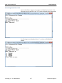
Table of Contents
1.
2.
RELATED PUBLICATIONS .......................................................................................................................... 5
GENERAL INFORMATION ......................................................................................................................... 6
Ordering Information .............................................................................................................................. 8
KEY FEATURES........................................................................................................................................ 11
PCle Interface Features ......................................................................................................................... 12
Software ................................................................................................................................................ 12
ENGINEERING DESIGN KIT ................................................................................................................ 12
Windows ....................................................................................................................................... 12
VxWorks ........................................................................................................................................ 13
Linux .............................................................................................................................................. 13
3.
Signal Interface Products (XMC-7K325F and XMC-7K410F Models) ..................................................... 13
PREPARATION FOR USE ......................................................................................................................... 14
UNPACKING AND INSPECTION .............................................................................................................. 14
CARD CAGE CONSIDERATIONS ......................................................................................................... 14
Board Installation ............................................................................................................................. 14
P15 Primary XMC Connector ............................................................................................................ 15
P16 Secondary XMC Connector........................................................................................................ 15
Rear P4 Field I/O Connector ............................................................................................................. 16
Front Panel Field I/O Connector (XMC-7K325F and XMC-7K410F models) ..................................... 18
SFP+ Module Connectors (XMC-7K325 and XMC-7K410F models) ................................................. 19
Ethernet MAC IDs (XMC-7K325F and XMC-7K410F models) ........................................................... 19
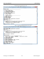
4.
Non-Isolation Considerations ................................................................................................................ 20
PROGRAMMING INFORMATION ........................................................................................................... 20
GETTING STARTED ................................................................................................................................. 20
FPGA Configuration .......................................................................................................................... 21
PCIe CONFIGURATION ADDRESS SPACE ........................................................................................... 21
CONFIGURATION REGISTERS ............................................................................................................ 22
BAR0 MEMORY MAP ............................................................................................................................. 23
CDMA MEMORY MAP............................................................................................................................ 24
INTERRUPT CONTROLLER ...................................................................................................................... 24
Interrupt Status Register .................................................................................................................. 25
Interrupt Pending Register ............................................................................................................... 26
Interrupt Enable Register ................................................................................................................. 26
Interrupt Acknowledge Register ...................................................................................................... 27
Set Interrupt Enable Register ........................................................................................................... 27
Clear Interrupt Enable Register ........................................................................................................ 28
Acromag, Inc. Tel: 248-295-0310
2
www.acromag.com
XMC-7 Series AXM/CC/F
USER’S MANUAL
Interrupt Vector Register ................................................................................................................. 28
Master Enable Register .................................................................................................................... 28
AXI-CDMA .............................................................................................................................................. 29
CDMA Control Register .................................................................................................................... 30
CDMA Status Register ...................................................................................................................... 32
CDMA Current Descriptor Pointer Register...................................................................................... 35
CDMA Tail Descriptor Pointer Register ............................................................................................ 36
CDMA Source Address Register........................................................................................................ 36
CDMA Destination Address Register ................................................................................................ 37
CDMA Bytes to Transfer Register ..................................................................................................... 38
Simple CDMA Programming Example .............................................................................................. 38
AXI-BAR0 Aperture Base Address..................................................................................................... 39
PCIe AXI-Bridge Control ......................................................................................................................... 39
PHY Status/Control Register............................................................................................................. 40
AXI Base Address Translation Configuration Register ...................................................................... 41
Aurora Status ......................................................................................................................................... 41
Control Register ..................................................................................................................................... 42
Flash Memory ........................................................................................................................................ 42
Write Protected Bitstream XMC-7A200/CC Models only ...................................................................... 44
AXI XADC Analog to Digital Converter (System Monitor) ...................................................................... 45
P1 Front I/O (XMC-7K325F and XMC-7K410F models only) .................................................................. 46
P1 Front Input Data Register ............................................................................................................ 46
P1 Front Output Data Register ......................................................................................................... 47
P1 Front Input Global Interrupt Enable Register.............................................................................. 48
P1 Front Input Channel Interrupt Enable Register ........................................................................... 48
P1 Front Input Channel Interrupt Status Register ............................................................................ 48
5.
P4 Rear Input Data Register .................................................................................................................. 48
P4 Rear Output Data Register ............................................................................................................... 49
P16 Input Data Register ......................................................................................................................... 50
P16 Output Data Register ...................................................................................................................... 51
THEORY OF OPERATION ........................................................................................................................ 52
PCI INTERFACE LOGIC ............................................................................................................................ 52
DDR3 Memory ....................................................................................................................................... 53
Clock Generation ................................................................................................................................... 53
Multi-Gigabit Transceivers .................................................................................................................... 53
32MB Linear BPI Flash ........................................................................................................................... 54
JTAG Port ............................................................................................................................................... 54
Encryption Key Storage ......................................................................................................................... 54
Acromag, Inc. Tel: 248-295-0310
3
www.acromag.com
XMC-7 Series AXM/CC/F
6.
7.
8.
USER’S MANUAL
Power System Devices ........................................................................................................................... 54
System Monitor ..................................................................................................................................... 56
FPGA FIRMWARE EXAMPLE DESIGN ..................................................................................................... 57
XMC-7A200/CC and XMC-7KxxxAX Models Block Diagram Overview .................................................. 57
XMC-7KxxxF Models Block Diagram ...................................................................................................... 63
XMC-7KxxxF Software............................................................................................................................ 69
Bootloader Memory Map ...................................................................................................................... 69
EchoServer Memory Map ...................................................................................................................... 69
DESIGN MODIFICATION WALK THROUGH............................................................................................. 70
Copy the Project ............................................................................................................................... 70
Modify the Source Files .................................................................................................................... 71
Modify the Constraints File .............................................................................................................. 85
Compile the Design .......................................................................................................................... 89
Generate Bitstream .......................................................................................................................... 91
Write Configuration File to Flash ..................................................................................................... 97
9.
10.
11.
SERVICE AND REPAIR ........................................................................................................................... 101
SERVICE AND REPAIR ASSISTANCE ...................................................................................................... 101
PRELIMINARY SERVICE PROCEDURE.................................................................................................... 101
WHERE TO GET HELP ........................................................................................................................... 101
SPECIFICATIONS ................................................................................................................................... 102
PHYSICAL.............................................................................................................................................. 102
POWER................................................................................................................................................. 102
PCIe BUS COMPLIANCE........................................................................................................................ 103
ENVIRONMENTAL ................................................................................................................................ 103
Certificate of Volatility ......................................................................................................................... 105
Accessories .......................................................................................................................................... 106
XMC-7K325F and XMC-7K410F Accessories ........................................................................................ 106
VHDCI Cable.................................................................................................................................... 106
SFP+ Direct Attach Cable ................................................................................................................ 107
1000BASE-T Copper SFP Transceiver ............................................................................................. 108
2.125 Gb/s Short-Wavelength SFP Transceiver.............................................................................. 109
12.
Revision History ................................................................................................................................... 111
Acromag, Inc. Tel: 248-295-0310
4
www.acromag.com
XMC-7 Series AXM/CC/F
USER’S MANUAL
All trademarks are the property of their respective owners.
IMPORTANT SAFETY CONSIDERATIONS
It is very important for the user to consider the possible adverse effects of power, wiring, component, sensor,
or software failures in designing any type of control or monitoring system. This is especially important where
economic property loss or human life is involved. It is important that the user employ satisfactory overall
system design. It is agreed between the Buyer and Acromag, that this is the Buyer's responsibility.
The information contained in this manual is subject to change without notice. Acromag, Inc. makes no warranty
of any kind with regard to this material, including, but not limited to, the implied warranties of merchantability
and fitness for a particular purpose. Further, Acromag, Inc. assumes no responsibility for any errors that may
appear in this manual and makes no commitment to update, or keep current, the information contained in this
manual. No part of this manual may be copied or reproduced in any form, without the prior written consent of
Acromag, Inc.
1. RELATED PUBLICATIONS
The following manuals and part specifications provide the necessary information for in depth understanding of
the board and the Xilinx Vivado development environment..
Kintex-7 FPGAs Data Sheet: DC and AC Switching Characteristics
ds182
7 Series FPGAs Memory Resources User Guide
ug473
7 Series FPGAs Configurable Logic Block User Guide
ug474
7 Series FPGAs SelectIO Resources User Guide
ug471
7 Series FPGAs Clocking Resources User Guide
ug472
7 Series DSP48E1 Slice User Guide
ug479
7 Series FPGAs GTX/GTH Transceivers User Guide
ug476
7 Series FPGAs Integrated Block for PCI Express v3.0 Product Guide
pg054
Zynq-7000 AP SoC and 7 Series Devices Memory Interface Solutions v2.3 User
Guide
ug586
Vivado Design Suite Tutorial Design Flows Overview
ug888
Vivado Design Suite Tutorial Designing IP Subsystems Using IP Integrator
ug995
AXI Reference Guide
ug761
Methods for Integrating AXI4-based IP Using Vivado IP Integrator
xapp1204
LogiCORE IP AXI GPIO v2.0 Product Guide
pg144
Acromag, Inc. Tel: 248-295-0310
5
www.acromag.com
XMC-7 Series AXM/CC/F
USER’S MANUAL
LogiCORE IP AXI Central Direct Memory Access v4.1 Product Guide for Vivado
Design Suite
pg034
LogiCORE IP AXI Interconnect v2.1 Product Guide
pg059
LogiCORE IP AXI Interrupt Controller (INTC) v4.1 Product Guide for Vivado Design
Suite
pg099
LogiCORE IP AXI XADC (v1.00a)
pg019
LogiCORE IP AXI EMC v3.0 Product Guide
pg100
LogiCORE IP AXI Bridge for PCI Express v2.5
pg055
7 Series FPGAs and Zynq-7000 All Programmable SoC XADC Dual 12-Bit 1 MSPS
Analog-to-Digital Converter User Guide
ug480
Clocking Wizard v5.1 LogiCORE IP Product Guide
pg065
Zynq-7000 AP SoC and 7 Series Devices Memory Interface Solutions (v2.2)
ds176
Vivado Design Suite User Guide Embedded Processor Hardware Design
ug898
AXI Ethernet Subsystem v6.2
pg138
LogiCORE IP AXI DMA v7.1
pg021
AXI IIC Bus Interface v2.0
pg090
LogiCORE IP AXI UART Lite v2.0
pg142
LogiCORE IP AXI Timer v2.0
pg079
DDR3L-RS 2Gb memory MT41K128M16JT-125IT:K Spec.
www.micron.com
Parallel Nor FLASH PC28F512G18FE
www.micron.com
ANSI/VITA 42.0 2008 standard
ANSI/VITA 42.3-2006
ANSI/VITA 46.0 2007 standard
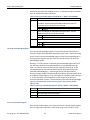
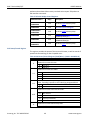
2. GENERAL INFORMATION
The XMC-7 series modules are XMC modules with the heart of the design
being a Xilinx 7 series reprogrammable FPGA. Re-configuration of the FPGA is
possible via a direct download into the Flash configuration memory over the
PCIe bus. The on board Flash memory loaded with configuration data allows
automatic configuration of the FPGA on power-up.
Acromag, Inc. Tel: 248-295-0310
6
www.acromag.com
XMC-7 Series AXM/CC/F
USER’S MANUAL
These modules include the following interfaces: Four or eight high speed
serial lanes are allocated to the XMC P15 connector. These lanes can be used
for PCIe (PCI Express), Serial RapidIO, or 10 Gigabit Ethernet. The example
design will support a four or eight lane Gen 1 PCIe implementation with one
DMA channel for data transfer between the PCIe bus and on board DDR3
memory.
Eight (four on XMC-xxxF models) high speed serial lanes are also allocated to
the XMC P16 connector. These serial lanes can be used for Serial RapidIO,
PCIe, Gigabit Ethernet, XAUI, or Xilinx Aurora. The example design will
support dual Aurora interfaces for use of these lanes. Two global clocks and
34 select I/O signals will also be provided on the P16 connector. Select I/O
signals are 2.5V I/O pins that can be selected from single-ended I/O standards
(LVCMOS, HSTL, and SSTL) and differential I/O standards (LVDS, HT, LVPECL,
BLVDS, Differential HSTL and SSTL).
The P4 rear I/O connector will provide two global clock differential pairs, and
30 LVDS signal pairs.
The board features 128 Meg x 64-bit DDR3 SDRAM and 32 Meg x 16-bit
parallel Flash. The parallel Flash provides storage for both the FPGA
configuration data and MicroBlaze CPU program storage.
MODELS
FRONT I/O
XMC-7A200
AXM modules
8 lanes
2 global clocks diff
pairs, 17 LVDS signal
pairs
2 global clocks diff pairs,
30 LVDS signal pairs
XMC-7A200CC
N/A
8 lanes
2 global clocks diff
pairs, 17 LVDS signal
pairs
2 global clocks diff pairs,
30 LVDS signal pairs
XMC-7KxxxAX
AXM modules
8 lanes
1 global clock diff pair,
15 LVDS signal pairs
2 global clocks diff pairs,
30 LVDS signal pairs
XMC-7KxxxCC
N/A
8 lanes
2 global clocks diff
pairs, 17 LVDS signal
pairs
2 global clocks diff pairs,
30 LVDS signal pairs
XMC-7KxxxF
2 SFP+, USB, JTAG,
2 global clock diff pairs,
11 LVDS signal pairs
4 lanes
2 global clocks diff
pairs, 17 LVDS signal
pairs
2 global clocks diff pairs,
30 LVDS signal pairs
Acromag, Inc. Tel: 248-295-0310
P16 HS
SERIAL
P16 SELECT I/O
7
P4 SELECT I/O
www.acromag.com
XMC-7 Series AXM/CC/F
USER’S MANUAL
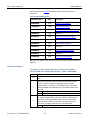
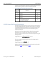
Ordering Information
The following table lists the orderable models and their corresponding
operating temperature range. These maximum operating temperatures are
determined using 75 % of the DSP slices and block RAMs at 200 MHz
operating frequency. The amount of FGPA resources and clock frequency
used by your application, if less than our test conditions, will possibly allow a
higher operating temperature.
Models XMC-7A200CC, XMC-7K325CC and XMC-7K410CC are conductioncooled models without front I/O.
Table 1 The XMC-7 series boards are available in these configurations.
MODELS
FPGA
OPERATING TEMPERATURE RANGE
XMC-7A200
Artix-7 XC7A200T
-40C to +55C (500 LFM airflow)1
XMC-7A200CC Artix-7 XC7A200T
-40C to +75 C cold-plate2
XMC-7K325AX
Kintex-7 XC7K325T
-40C to +45C (500 LFM airflow)
XMC-7K410AX
Kintex-7 XC7K410T
-40C to +40C (500 LFM airflow)
XMC-7K325CC
Kintex-7 XC7K325T
-40C to +70C cold-plate3
XMC-7K410CC
Kintex-7 XC7K410T
-40C to +70C cold-plate4
XMC-7K325F
Kintex-7 XC7K325T
-40C to +55C (500 LFM airflow)
XMC-7K410F
Kintex-7 XC7K410T
-40C to +55C (500 LFM airflow)
1
Tested on Acromag VPX4820 carrier with 500 LFM airflow
Tested on Acromag VPX4820-CC carrier with thermal interface material (Berquist Gap Pad 1500R) between the carrier
cold plate and the XMC module heatsink.
3
Tested on Acromag VPX4820-CC carrier with thermal interface material (Berquist Gap Pad 1500R ) between the carrier
cold plate and the XMC module heatsink.
4
Tested on Acromag VPX4820-CC carrier with thermal interface material (Berquist Gap Pad 1500R ) between the carrier
cold plate and the XMC module heatsink.
2
Acromag, Inc. Tel: 248-295-0310
8
www.acromag.com
XMC-7 Series AXM/CC/F
USER’S MANUAL
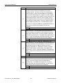
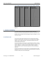
P1
AXM Connector
44 LVDS Pairs,
2 Global Clock Pairs,
4 LVTTL I/O
JTAG
AXM Models
U8-U11
U8-U11
DDR3
SDRAM
U8-U11
DDR3
128MSDRAM
x 16 = 2Gb
DDR3
SDRAM
128M
x
16
= 2Gb
x4 => 8Gb
or 1GB
DDR3 SDRAM
128M=>
x 16 = 2Gb
128Mx4
x 16 =8Gb
2Gbor 1GB
x4 => 8Gb or 1GB
x4 => 8Gb or 1GB
16 x 4
DIP Switch 1
BPI & Platform Flash Memory
Configuration Control
(8 position SMT Switch)
Xilinx 7 Series FPGA
Artix XC7A200T or
Kintex XC7K325T or XC7K410T
x4
16 x 1
x4
BPI Flash Memory
(Bite-wide Peripheral Interface}
FPGA Configuration and MicroBlaze
CPU Instruction Storage
32M x 16 = 512Mb or 64MB
IPMI Serial EEPROM
512 x 8 = 4Kb
or 512B
x4 Artix
x8 Kintex
PCIe
JTAG
34 (30) I/O
&
2 (1) Global Clock Pairs
CC (AXM)
x4
(hardware
example
design
Aurora)
x4
(hardware
example
design
Aurora)
IPMI
P15
VITA 42 XMC Connector
P16
VITA 42 XMC Connector
30 LVDS
pairs &
2 Global
Clock
Pairs
J4
64 pin Rear I/O Connector
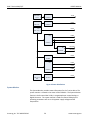
Figure 1 Block Diagram AXM / CC Models
Acromag, Inc. Tel: 248-295-0310
9
www.acromag.com
XMC-7 Series AXM/CC/F
USER’S MANUAL
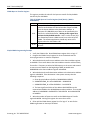
P5
Front I/O 36 position VHDCR Connector
P1
Small Form-factor
Pluggable (SFP+) Port #1
11 LVDS Pairs
& 2 Global
Clock Pairs
JTAG
P2
Small Form-factor
Pluggable (SFP+) Port #2
USB
USB to UART
Bridge
U8-U11
U8-U11
DDR3
SDRAM
U8-U11
DDR3
128MSDRAM
x 16 = 2Gb
DDR3
128M
x 16
= 2Gb
x4 SDRAM
=>
8Gb
or 1GB
DDR3
SDRAM
128M=>
x 16 = 2Gb
128Mx4
x 16 =8Gb
2Gbor 1GB
x4 => 8Gb or 1GB
x4 => 8Gb or 1GB
UART
x1
x1
16 x 4
Xilinx 7 Series FPGA
Kintex XC7K325T or XC7K410T
x2
16 x 1
x2
BPI Flash Memory
(Bite-wide Peripheral Interface}
FPGA Configuration and MicroBlaze
CPU Instruction Storage
32M x 16 = 512Mb or 64MB
IPMI Serial EEPROM
512 x 8 = 4Kb
or 512B
34 I/O
&
2 Global
Clock
Pairs
x8
PCIe
JTAG
x2
(hardware
example
design
Aurora)
x2
(hardware
example
design
Aurora)
IPMI
P15
VITA 42 XMC Connector
P16
VITA 42 XMC Connector
30 LVDS
pairs &
2 Global
Clock
Pairs
J4
64 pin Rear I/O Connector
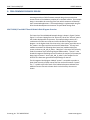
Figure 2 Block Diagram F Models
Acromag, Inc. Tel: 248-295-0310
10
www.acromag.com
XMC-7 Series AXM/CC/F
USER’S MANUAL
KEY FEATURES
The block diagram shown in Figure 1 illustrates the key features listed below.
Features common to all models are listed first, followed by model specific
features.
Common Features:
• Reconfigurable Xilinx FPGA –The FPGA loads its configuration data from
flash memory each time power is applied to the module. The host processor
can be used to change the flash configuration memory via the PCIe bus. This
provides a means for creating custom user defined designs. The FPGA will
configure from the updated flash memory on the next power cycle.
•
DDR3 SDRAM –128 Meg x 64-bit DDR3 SDRAM is connected to the FPGA.
• Interface to Rear P4 Connector – The FPGA is directly connected to 64
pins of the rear P4 connector. All 2.5 Volt I/O standards supported by the
Xilinx 7 series devices are available. The example design implements LVCMOS
single ended signaling.
• P15 High Speed Interface –Eight high speed serial lanes are allocated to
the XMC P15 connector. These lanes can be used for an 8 lane PCIe (PCI
Express) implementation, Serial RapidIO, or 10 Gigabit Ethernet. The Kintex
example design includes an 8 lane Gen 1 PCIe implementation while the Artix
example design includes a 4 lane Gen 1 PCIe implementation.
Features supported on AX models:
• Acromag AXM Module Support – various mezzanine modules (“AXM”
model prefix), ordered separately, allow the user to select the Front I/O
required for their application.
• P16 High Speed Interface – Eight high speed serial lanes are allocated to
the XMC P16 connector in the AX models. These lanes can be used for Serial
RapidIO, PCIe, 10 Gigabit Ethernet, or Xilinx Aurora. The example design
supports a pair of four lane Aurora interfaces in a chip to chip loopback
implementation.
Features supported on CC models:
• P16 High Speed Interface – Eight high speed serial lanes are allocated to
the XMC P16 connector in the CC model. These lanes can be used for Serial
RapidIO, PCIe, 10 Gigabit Ethernet, or Xilinx Aurora. The example design
supports a pair of four lane Aurora interfaces in a chip to chip loopback
implementation.
Features supported on F models:
• P16 High Speed Interface – Four high speed serial lanes are allocated to
the XMC P16 connector on the F model. These lanes can be used for Serial
RapidIO, PCIe, or Xilinx Aurora. The example design supports a pair of two
lane Aurora interfaces in a chip to chip loopback implementation.
Acromag, Inc. Tel: 248-295-0310
11
www.acromag.com
XMC-7 Series AXM/CC/F
USER’S MANUAL
• Interface to Front I/O Connector – The FPGA is directly connected to a
front I/O connector. All 2.5 Volt I/O standards supported by the Xilinx 7 series
devices are available on 13 signal pairs. A JTAG port is included for
configuration and for use with the Xilinx ChipScope FPGA debugger. The USB
UART interface provides a COMM port device for the host processor to
connect to the MicroBlaze UART.
• Example Design Provided – The example design includes implementation
of the DDR3 memory, PCIe bus 8 lane Gen 1, control of digital front and rear
I/O, and 1 Gig Ethernet 1000-X interface to the SFP+ modules.
PCle Interface Features
• PCIe Bus – The example design includes a PCI Express Generation 1
interface operating at a bus speed of 2.5 Gbps per lane per direction. On
Kintex based models eight lanes are supported. Artix models support 4 lanes.
Maximum payload size is 1024 bytes. Up to 4 GBytes/sec burst data transfer
rate can be achieved when utilizing eight lanes.
• PCIe Bus Master – The PCIe interface logic becomes the bus master to
perform DMA transfers.
• DMA Operation – The example design includes a DMA controller to move
data between the DDR3 memory and the PCIe bus interface.
• Compatibility – PCI Express Base Specification v2.1 compliant PCI Express
Endpoint. Provides one multifunction interrupt. The XMC-7 series modules
are compatible with XMC VITA 42.3 specification for P15.
Software
The XMC-7 series products require support drivers specific to your operating
system. Supported operating systems include: Linux, Windows, and VxWorks.
ENGINEERING DESIGN KIT
Acromag provides an engineering design kit for the XMC products (sold
separately), a “must buy” for first time 7 series module purchasers. The
design kit (model XMC-7KA-EDK) provides the user with the basic information
required to develop a custom FPGA program for download to the Xilinx FPGA.
The design kit includes a CD containing: schematics, parts list, part location
drawing, example VHDL source, and other utility files. The 7 series modules
are intended for users fluent in the use of Xilinx FPGA design tools.
Windows
Acromag provides software products (sold separately) to facilitate the
development of Windows applications interfacing with Acromag PMC, XMC,
and VPX I/O board products, PCI and PCIe I/O Cards, and CompactPCI I/O
Cards. This software (model PCISW-API-WI) consists of low-level drivers and
Dynamic Link Libraries (DLLs) that are compatible with a number of
Acromag, Inc. Tel: 248-295-0310
12
www.acromag.com
XMC-7 Series AXM/CC/F
USER’S MANUAL
programming environments. The DLL functions provide a high-level interface
to boards eliminating the need to perform low-level reads/writes of registers,
and the writing of interrupt handlers.
VxWorks
Acromag provides a software product (sold separately) consisting of
VxWorks software. This software (Model PMCSW-API-VXW) is composed of
VxWorks (real time operating system) libraries for all Acromag PMC, XMC,
and VPX I/O board products, PCI and PCIe I/O Cards, and CompactPCI I/O
Cards. The software is implemented as a library of “C” functions which link
with existing user code to make possible simple control of all Acromag PCI
and PCIe boards.
Linux
Acromag provides a software product consisting of Linux software. This
software (Model PMCSW-API-LNX) is composed of Linux libraries for all
Acromag PMC, XMC, and VPX I/O board products, PCI and PCIe I/O cards, and
CompactPCI I/O cards. The software supports X86 PCI bus only and is
implemented as library of “C” functions which link with existing user code to
make possible simple control of all Acromag PCI and PCIe boards.
Signal Interface Products (XMC-7K325F and XMC-7K410F Models)
Accessory cables that interface to the front VHDCI connector and SFP+ ports
are available from Acromag.
VHDCI Cable
Acromag provides a cable that brings the 36 pins of the VHDCI front I/O
connector out to a 50 pin SCSI connector. The Acromag part number is
5025-921. See Table 5 Front VHDCI Field I/O Pin Connections. A cable
drawing is also provided in the accessories section at the end of this manual.
Direct Attach Cable
Acromag provides a 1 meter direct attach cable that connects one SFP+ port
to another SFP+ port. This passive cable can be used to carry 10 Gb Ethernet
or Aurora signals to another nearby XMC-7Kxxx module. The Acromag part
number is TAPCABLE1M. A cable drawing is provided in the accessories
section at the end of this manual.
1000BASE-T Copper SFP Transceiver
Acromag provides a Copper SFP Transceiver that is compatible with the
Gigabit Ethernet and 1000BASE-T standards as specified in IEEE Std 802.3. It
has an RJ-45 connector and is RoHS compliant and lead-free. The Acromag
part number is 5028-455. A cable drawing is provided in the accessories
section at the end of this manual.
2.125 Gb/S Short-Wavelength SFP Transceiver
Acromag, Inc. Tel: 248-295-0310
13
www.acromag.com
XMC-7 Series AXM/CC/F
USER’S MANUAL
Acromag provides 2.125 Gb/s Short Wavelength SFP Transceiver that is
compatible with the Gigabit Ethernet standard as specified in IEEE Std 802.3
and Fibre Channel FC-PI-2 Rev. 5.0. It is RoHS compliant and lead-free. It
supports up to 2.125 Gb/s bi-directional data links. The module uses an
850nm Oxide VCSEL laser transmitter. The Acromag part number is 5028-452.
A drawing is provided in the accessories section at the end of this manual.
3. PREPARATION FOR USE
UNPACKING AND INSPECTION
Upon receipt of this product, inspect the shipping carton for evidence of
mishandling during transit. If the shipping carton is badly damaged or water
stained, request that the carrier's agent be present when the carton is
opened. If the carrier's agent is absent when the carton is opened and the
contents of the carton are damaged, keep the carton and packing material for
the agent's inspection.
For repairs to a product damaged in shipment, refer to the Acromag Service
Policy to obtain return instructions. It is suggested that salvageable shipping
cartons and packing material be saved for future use in the event the product
must be shipped.
This board is physically protected with packing material and electrically
protected with an anti-static bag during shipment. It is recommended that the
board be visually inspected for evidence of mishandling prior to applying
power.
The board utilizes static sensitive components and should only be handled at
a static-safe workstation.
CARD CAGE CONSIDERATIONS
Refer to the specifications for loading and power requirements. Be sure that
the system power supplies are able to accommodate the power requirements
of the carrier board, plus the installed XMC module, within the voltage
tolerances specified.
Adequate air circulation must be provided to prevent a temperature rise
above the maximum operating temperature and to prolong the life of the
electronics. If the installation is in an industrial environment and the board is
exposed to environmental air, careful consideration should be given to airfiltering.
Board Installation
Remove power from the system before installing board, cables, termination
panels, and field wiring.
Acromag, Inc. Tel: 248-295-0310
14
www.acromag.com
XMC-7 Series AXM/CC/F
USER’S MANUAL
P15 Primary XMC Connector
The P15 XMC connector is wired per the VITA 42.0 standard. Most of the P15
signals connect directly to the user programmable FPGA. The P15 connector
provides the 8 lane PCI Express interface to the host processor, a JTAG
interface, and an I2C interface to a serial memory device. XMC-7A200,
XMC-7K325AX, and XMC-7K410AX models require 12V and -12V power when
an AXM module is installed that requires +12V and -12V power. All models
require 3.3AUX power in order to maintain the encryption key stored in
volatile memory, if that feature is required. The JTAG signals connect to the
FGPA for configuration and debugging.
Table 2 P15 Primary XMC Connector
Pin
1
2
3
4
5
6
7
8
9
10
11
12
13
14
15
16
17
18
19
A
B
C
PET00+
PET00+3.3V
GND
GND
TRST#
PET02+
PET02+3.3V
GND
GND
TCK
PET04+
PET04+3.3V
GND
GND
TMS
PET06+
PET06+3.3V
GND
GND
TDI
N.C.
N.C.
N.C.
GND
GND
TDO
PER00+
PER00MBIST#
GND
GND
GA1
PER02+
PER02- +3.3AUX
GND
GND
GA2
PER04+
PER04N.C.
GND
GND
MVMRO
PER06+
PER06N.C.
GND
GND
N.C.
REFCLK0_P REFCLK0_N N.C.
D
PET01+
GND
PET03+
GND
PET05+
GND
PET07+
GND
N.C.
GND
PER01+
GND
PER03+
GND
PER05+
GND
PER07+
GND
WAKE#
E
F
PET01- VPWR
GND
MRSTI#
PET03- VPWR
GND MRSTO#
PET05- VPWR
GND
+12V
PET07- VPWR
GND
-12V
N.C.
VPWR
GND
GA0
PER01- VPWR
GND MPRSNT#
PER03- VPWR
GND
MSDA
PER05- VPWR
GND
MSCL
PER07N.C.
GND
N.C.
ROOT#
N.C.
P16 Secondary XMC Connector
The P16 secondary XMC connector connects directly to the userprogrammable FPGA for both high speed Giga bit data signals and standard
I/O user signals. The user I/O pins are connected to FPGA banks with VCCO
pins powered by 2.5 volts. Thus these user I/O pins support the 2.5 volt I/O
standards. The IOSTANDARD attribute can be set in the design constraints file
(.xdc). For example, P16 user I/O can be defined for LVDS_25 (Low-Voltage
Differential Signaling). The example design configures the P16 I/O as
LVCMOS25 (low voltage CMOS) in the design constraints file. The tables
included in the P16 Input Data Register and P16 Output Data Register sections
Acromag, Inc. Tel: 248-295-0310
15
www.acromag.com
XMC-7 Series AXM/CC/F
USER’S MANUAL
can be used to map the LVCMOS signal to the signal names given in this table.
The 2.5 volt I/O standards available are listed in the 7 Series FPGAs SelectIO
Resources User Guide available from Xilinx.
Table 3 P16 Secondary XMC Connections
Pin
1
2
3
4
5
6
7
8
9
10
11
12
13
14
15
16
17
18
19
A
B
C
DP00+
DP00S18G_N
GND
GND
S16_N
DP02+
DP02S16_P
GND
GND
S14_N
DP04+
DP04S14_P
GND
GND
S12_N
DP06+
DP06S12_P
GND
GND
S10_N
5
N.C.
N.C.
S10_P
GND
GND
S8_N
DP10+
DP10S8_P
GND
GND
S6_N
DP12+
DP12S6_P
GND
GND
S4_N
DP14+
DP14S4_P
GND
GND
S2_N
DP16+
DP16S2_P
GND
GND
S0G_N
REFCLK0_P REFCLK0_N S0G_P
D
E
DP01+
DP01GND
GND
DP03+
DP03GND
GND
DP05+
DP05GND
GND
DP07+
DP07GND
GND
N.C.
N.C.
GND
GND
DP11+
DP11GND
GND
DP13+
DP13GND
GND
DP15+
DP15GND
GND
DP17+
DP17GND
GND
N.C. ROOT0_N
F
S18G_P
S17_N
S17_P
S15_N
S15_P
S13_N
S13_P
S11_N
S11_P
S9_N
S9_P
S7_N
S7_P
S5_N
S5_P
S3_N
S3_P
S1_N
S1_P
The example design implements 2.5 volt LVCMOS I/O at the P16 connector.
Alternatively, 2.5 volt LVDS I/O can be used on the P16 connector.
Configured as LVDS signal pairs, the signals can be grouped to match the
ANSI/VITA 46.0 X38s pattern map. A total of 19 differential signal pairs are
provided (16 on AX models). These differential signal pairs connect to column
C and F of the P16 XMC connector as shown in Table 3. For example S3_P and
S3_N form a signal pair. There are two global clock differential pairs available
(S0G_P, S0G_N) and (S18G_P, S18G_N). The P identifies the Positive input,
the N identifies the Negative input.
The XMC P16 Secondary connector is a 114-pin Samtec ASP-103614-05
connector. The connector complies with ANSI/VITA 42.3-2006.
Rear P4 Field I/O Connector
The rear I/O P4 connector connects directly to the user-programmable FPGA.
The VCCO pins are powered by 2.5 volts and thus will support the 2.5 volt I/O
standards. The IOSTANDARD attribute can be set in the design constraints file
5
N.C. – not connected
Acromag, Inc. Tel: 248-295-0310
16
www.acromag.com
XMC-7 Series AXM/CC/F
USER’S MANUAL
(XDC). The example design configures the rear P4 I/O as LVCMOS25 (low
voltage CMOS) in the design constraints file. The tables included in the P4
Rear Input Data Register and P4 Rear Output Data Register sections can be
used to map the LVCMOS signal to the signal names given in the table below.
The rear I/O can alternatively be configured for LVDS_25 (Low-Voltage
Differential Signaling) in the design constraints file. The 2.5 volt I/O standards
available are listed in the 7 Series FPGAs SelectIO Resources User Guide
available from Xilinx.
Two of the signal pairs (RIO0_GCLK_P/N and RIO31_CCLK_P/N) are connected
to clock capable I/O pins on the FPGA. These pins provide a direct path to
global clock buffers in the FPGA.
As LVDS signal pairs, the signals can be grouped as 32 LVDS I/O pairs. The
LVDS pairs are arranged in the same row in Table 4. For example, RIO1_P and
RIO1_N form a signal pair. The P identifies the Positive input while the N
identifies the Negative input.
Table 4 Rear Field I/O Pin Connections
Ch.
0
1
2
3
4
5
6
7
8
9
10
11
12
13
14
15
16
17
18
19
20
21
22
23
24
25
26
Acromag, Inc. Tel: 248-295-0310
Positive Pin Description
RIO0_GCLK_P
RIO1_P
RIO2_P
RIO3_P
RIO4_P
RIO5_P
RIO6_P
RIO7_P
RIO8_P
RIO9_P
RIO10_P
RIO11_P
RIO12_P
RIO13_P
RIO14_P
RIO15_P
RIO16_P
RIO17_P
RIO18_P
RIO19_P
RIO20_P
RIO21_P
RIO22_P
RIO23_P
RIO24_P
RIO25_P
RIO26_P
17
Pin
1
2
5
6
9
10
13
14
17
18
21
22
25
26
29
30
33
34
37
38
41
42
45
46
49
50
53
Negative Pin Description
RIO0_GCLK_N
RIO1_N
RIO2_N
RIO3_N
RIO4_N
RIO5_N
RIO6_N
RIO7_N
RIO8_N
RIO9_N
RIO10_N
RIO11_N
RIO12_N
RIO13_N
RIO14_N
RIO15_N
RIO16_N
RIO17_N
RIO18_N
RIO19_N
RIO20_N
RIO21_N
RIO22_N
RIO23_N
RIO24_N
RIO25_N
RIO26_N
Pin
3
4
7
8
11
12
15
16
19
20
23
24
27
28
31
32
35
36
39
40
43
44
47
48
51
52
55
www.acromag.com
XMC-7 Series AXM/CC/F
USER’S MANUAL
Ch.
27
28
29
30
31
Positive Pin Description
RIO27_P
RIO28_P
RIO29_P
RIO30_P
RIO31_GCLK_P
Pin
54
57
58
61
62
Negative Pin Description
RIO27_N
RIO28_N
RIO29_N
RIO30_N
RIO31_GCLK_N
Pin
56
59
60
63
64
The example design implements 2.5volt LVCMOS I/O to the rear connector.
Alternatively, 2.5volt LVDS I/O can be used on the rear connector.
This connector is a 64-pin female receptacle header (AMP 120527-1 or
equivalent) which mates to the male connector on the carrier board (AMP
120521-1 or equivalent).
Front Panel Field I/O Connector (XMC-7K325F and XMC-7K410F models)
The front panel provides access to a 36 pin VHDCI connector and two SFP+
port connectors. The VHDCI connector provides interfaces to JTAG, USB and
26 single ended or 13 differential I/O signal pairs. Two of the signal pairs are
routed to global clock pins on the Kintex 7 device.
The 26 front I/O signals connect directly to the user-programmable FPGA. The
VCCO pins are powered by 2.5 volts and thus will support the 2.5 volt I/O
standards. The IOSTANDARD attribute can be set in the user constraints file
(UCF). The example design configures the Front I/O as LVCMOS25 (low
voltage CMOS) in the user constraints file. The tables included in the Front
Input Data Register and Front Output Data Register sections can be used to
map the LVCMOS signals to the signal names given in the table below.
The Front I/O can alternatively be defined for LVDS_25 (Low-Voltage
Differential Signaling) in the user constraints file. The 2.5 volt I/O standards
available are listed in the Kintex-7 User Guide available from Xilinx.
Table 5 Front VHDCI Field I/O Pin Connections
Ch.
0
1
2
3
4
5
6
7
Acromag, Inc. Tel: 248-295-0310
Positive Pin
TCK
TDO
GND
FIO0_P
FIO1_P
FIO2_P
FIO3_P
FIO4_P
FIO5_P
FIO6_P
FIO7_P
Pin
1
2
3
4
5
6
7
8
9
10
11
18
Negative Pin
TMS
TDI
+2.5V
FIO0_N
FIO1_N
FIO2_N
FIO3_N
FIO4_N
FIO5_N
FIO6_N
FIO7_N
Pin
19
20
21
22
23
24
25
26
27
28
29
www.acromag.com
XMC-7 Series AXM/CC/F
USER’S MANUAL
Ch.
8
9
10
11
12
Positive Pin
FIO8_P
FIO9_P
FIO10_P
FIO11_GCLK_P
FIO12_GCLK_P
USB_D+
USB_VBUS(from host)
Pin
12
13
14
15
16
17
18
Negative Pin
FIO8_N
FIO9_N
FIO10_N
FIO11_GCLK_N
FIO12_GCLK_N
USB_DGND
Pin
30
31
32
33
34
35
36
The example design implements 2.5volt LVCMOS I/O at the front connector.
Alternatively, 2.5volt LVDS I/O can be used on the front connector.
This connector is a 36-pin female receptacle header
(SAMTEC VHDCR-36-01-M-RA or equivalent) which mates to the male
connector.
SFP+ Module Connectors (XMC-7K325 and XMC-7K410F models)
Table 6 SFP+ Module Pin Connections
Pin
1
2
3
4
5
6
7
8
9
10
11
12
13
14
15
16
17
18
19
20
Symbol
VeeT
Tx_Fault
Tx_Disable
SDA
SCL
Mod_ABS
RS0
Rx_LOS
VeeR
VeeR
VeeR
RDRD+
VeeR
VccR
VccT
VeeT
TD+
TDVeeT
Pin Description
Module Transmitter Ground
Module Transmitter Fault
Transmitter Disable
2-wire Serial Interface Data Line
2-wire Serial Interface Clock
Module Absent
Rate Select
Receive Loss of Signal Indication
Module Receiver Ground
Module Receiver Ground
Module Receiver Ground
Receiver Inverted Data Output
Receiver Non-Inverted Data Output
Module Receiver Ground
Module Receiver 3.3 V Supply
Module Transmitter 3.3 V Supply
Module Transmitter Ground
Transmitter Non-Inverted Data Input
Transmitter Inverted Data Input
Module Transmitter Ground
Ethernet MAC IDs (XMC-7K325F and XMC-7K410F models)
Two Ethernet MAC ID (address) numbers have been reserved for each
XMC-7K325F and XMC-7K410F units. The numbers are printed on the labels
attached to the board. The example design provided by Acromag includes
MicroBlaze software running the LWIP TCP/IP network protocol suite. The
Acromag, Inc. Tel: 248-295-0310
19
www.acromag.com
XMC-7 Series AXM/CC/F
USER’S MANUAL
MAC ID for each port is set by the software. If your application uses the
example design as a base for your project, replace the MAC IDs in the “C”
source with the IDs printed on the label.
Non-Isolation Considerations
The board is non-isolated, since there is electrical continuity between the
logic and field I/O grounds. As such, the field I/O connections are not isolated
from the system. Care should be taken in designing installations without
isolation to avoid noise pickup and ground loops caused by multiple ground
connections.
4. PROGRAMMING INFORMATION
This Section provides the specific information necessary to program and
operate the board.
GETTING STARTED
1. The XMC-7 series modules are shipped with the example design FPGA
bitstream stored in the flash memory. This example design bitstream
operates with the driver software included in the support package. Upon
power-up the XMC-7 series module will automatically configure the FPGA
with the example design bitstream stored in flash. As a first step become
familiar with the appropriate example design for your model. The board will
perform all the functions of the example design as described in this manual.
The Example Design Memory Map section gives a description of the I/O
registers provided by the example design. It will allow testing of PCIe
interface, read/write of DDR3 memory, all digital I/O ports, interrupts, P16
Aurora loopback, and DMA operation. It is strongly recommended that you
become familiar with the board features by using the example design as
provided by Acromag.
CAUTION: Do not attempt to reconfigure the flash memory until after you
have tested and become familiar with the XMC-7 series module as provided in
the example design.
2. After you are familiar with the module’s features and have tested it using
the example design, proceed to the DESIGN MODIFICATION WALK THROUGH.
Here you will modify the example design VHDL code slightly. The
configuration flash must be overwritten to test your design. Once the flash is
erased you will not be able to go back to the example design by simply
powering down and restarting the board. If your code does not function as
desired you may need to reload the Acromag design example. You can reload
the Acromag example design via the JTAG port using the Xilinx Vivado tool.
Upon power-up, the example design provided by Acromag will again be
loaded into the FPGA. Note: XMC-7A200AX/CC models are delivered with two
copies of the example design bitstream stored in flash memory. One of the
copies is stored in a write protected section of the flash. If the configuration
Acromag, Inc. Tel: 248-295-0310
20
www.acromag.com
XMC-7 Series AXM/CC/F
USER’S MANUAL
file loaded from the writeable section of flash fails to support the flash write
function via the PCIe bus, a recovery method is available. The FPGA can be
directed to configure from the backup bitstream by opening switch SW1
position 3 shown in Figure 3.
See the Flash Configuration section for a description of the steps required to
write new data or to reprogram the example design code to the flash device.
Figure 3 XMC-7A200 Switch Location
FPGA Configuration
The XMC-7 series modules support configuration in the following modes:
•
Master BPI-Up using Linear BPI Flash device.
•
JTAG using Xilinx external program cable.
The FPGA configuration bitstream is loaded from flash memory on power-up.
PCIe CONFIGURATION ADDRESS SPACE
This XMC-7 series modules are PCI Express Base Specification Revision v2.1
compliant.
The PCIe bus is defined to address three distinct address spaces: I/O, memory,
and configuration space. This board can be accessed via the PCIe bus
memory, and configuration spaces.
The card’s configuration registers are initialized by system software at powerup to configure the card. The board is a Plug-and-Play PCIe card. As a Plugand-Play card the board’s base address and system interrupt request are not
selected via jumpers but are assigned by system software upon power-up via
the configuration registers. A PCIe bus configuration access is used to
read/write the PCIe card’s configuration registers.
When the computer is first powered-up, the computer’s system configuration
software scans the PCIe bus to determine what PCIe devices are present. The
software also determines the configuration requirements of the PCIe card.
The system software accesses the configuration registers to determine how
many blocks of memory space the module requires. It then programs the
board’s configuration registers with the unique memory base address.
Acromag, Inc. Tel: 248-295-0310
21
www.acromag.com
XMC-7 Series AXM/CC/F
USER’S MANUAL
Since this board is not fixed in address space, its device driver must use the
mapping information stored in the board’s Configuration Space registers to
determine where the board is mapped in memory space.
The configuration registers are also used to indicate that the board requires
an interrupt request. The system software then programs the configuration
registers with the interrupt request assigned to the board.
CONFIGURATION REGISTERS
The PCIe specification requires software driven initialization and configuration
via the Configuration Address space. This board provides 512 bytes of
configuration registers for this purpose. It contains the configuration
registers shown in Table 7 to facilitate Plug-and-Play compatibility.
The Configuration Registers are accessed via the Configuration Address and
Data Ports. The most important Configuration Registers are the Base Address
Registers and the Interrupt Register which must be read to determine the
base address assigned to the board and the interrupt request that goes active
on a board interrupt request.
Table 7 Configuration Registers
Reg.
Num.
0
1
2
3
4:5
6:7
D31
D24
D16
D15
D8
D7
D0
Device ID
Vendor ID
0x7000 XMC-7K325F
0X7001 XMC-7K410F
16D5
0x7002 XMC-7K325AX
0x7003 XMC-7K410AX
0x7004 XMC-7K325CC
0x7005 XMC-7K410CC
0x7006 XMC-7A200
0x7007 XMC-7A200CC
Status
Command
Class Code=118000
Rev ID=00
BIST
Header
Latency
Cache
64-bit Memory Base Address for Memory Accesses to PCIe
interrupt, I/O registers, System Monitor registers, and Flash
memory.
4M Space (BAR0)
64-bit Memory Base Address for access to DDR3 memory.
16M Space (BAR2)
8:10
Acromag, Inc. Tel: 248-295-0310
D23
Not Used
22
www.acromag.com
XMC-7 Series AXM/CC/F
USER’S MANUAL
11
Subsystem ID
0x7000 XMC-7K325F
0x7001 XMC-7K410F
0x7002 XMC-7K325AX
0x7003 XMC-7K410AX
0x7004 XMC-7K325CC
0x7005 XMC-7K410CC
0x7006 XMC-7A200
0x7007 XMC-7A200CC
12
13,14
15
Max_Lat
Subsystem Vendor ID
16D5
Not Used
Reserved
Max_Lat
15
15
This board is allocated a 4M byte block of memory (BAR0), to access the PCIe
interrupt, I/O registers, XADC registers, and Flash memory. The PCIe bus
decodes 4M bytes for BAR0 for this memory space.
This board is also allocated a 16M byte block of memory (BAR2), to access
DDR3 memory. The PCIe bus decodes 16M bytes for BAR2 for this memory
space.
BAR0 MEMORY MAP
The BAR0 memory address space is used to access the PCIe interrupt, Front,
Rear, and P16 I/O registers, System Monitor registers, and Flash memory.
Note that the base address for the board (BAR0) in memory space must be
added to the addresses shown to properly access these registers.
Table 8 BAR0 Registers
BAR0 Base Address
0x0000_0000→0x0000_7FFF
Acromag, Inc. Tel: 248-295-0310
Size
Description
32K
Reserved
0x0000_8000→0x0000_8FFF
4K
AXM Module (see specific AXM
model user’s manual for
additional address detail)
0x0000_9000→0x0009_FFFF
604K
Reserved
0x000A_0000→0x000A_FFFF 64K
CDMA (see PG034)
0x000B_0000→0x000E_FFFF
256K
Reserved
0x000F_0000→0x000F_FFFF
64K
0x0010_0000→0x0010_FFFF
64K
0x0011_0000→0x002F_FFFF
1M
Reserved
0x0030_0000→0x0030_FFFF
64K
XADC System Monitor (see
DS790)
23
PCIe AXI Bridge Control
(see PG054)
Interrupt Controller
(see PG099)
www.acromag.com
XMC-7 Series AXM/CC/F
USER’S MANUAL
BAR0 Base Address
Size
Description
0x0031_0000→0x0031_FFFF
64K
P1 Front I/O AXI_GPIO
(XMC-7KxxxF models)
(see PG144)
0x0032_0000→0x0032_FFFF
64K
P16 I/O AXI_GPIO (see PG144)
0x0033_0000→0x0033_FFFF
64K
0x0034_0000→0x0034_FFFF
64K
0x0035_0000→0x00FF_FFFF
12M
P4 Rear I/O AXI_GPIO
(see PG144)
Aurora Control/Status
AXI_GPIO (see PG144)
Reserved
Note that any registers/bits not mentioned will remain at the default value:
logic low.
CDMA MEMORY MAP
The Central Direct Memory Access (CDMA) controller can access the following
devices: Flash memory, DDR3 memory, AXI to PCI bridge (BAR0), and the
control registers for the PCIe interface. Note that the PCIe interface cannot
directly access Flash memory; transfers to and from Flash must be initiated by
the CDMA controller. The CDMA controller includes the scatter gather
function. If used, the scatter gather descriptor list must be located in DDR3
memory.
BAR0 Base Address
Size
Description
0x0000_0000→0x000E_FFFF
960K
Reserved
0x000F_0000→0x000F_FFFF
64K
PCIe AXI Bridge Control
(see PG054)
0x0010_0000→0x5FFF_FFFF
1535M Reserved
0x6000_0000→0x63FF_FFFF
64M
Flash AXI_EMC (see PG100)
0x6400_0000→0x7FFF_FFFF
448M
Reserved
0x8000_0000→0xBFFF_FFFF
1G
DDR3 SDRAM
0xC000_0000→0xFFFF_FFFF
1G
Reserved
INTERRUPT CONTROLLER
The AXI Interrupt Controller concentrates multiple interrupt inputs from
peripheral devices to a single interrupt output to the system processor using
the PCIe bus. The interrupt controller contains programmer accessible
registers that allow interrupts to be enabled, queried and cleared under
software control over the PCIe bus interface.
Acromag, Inc. Tel: 248-295-0310
24
www.acromag.com
XMC-7 Series AXM/CC/F
USER’S MANUAL
Table 9 Interrupt Controller Registers
BAR0 Base Addr+
Bit(s)
Description
0x00100000
31:0
Interrupt Status Register
0x00100004
31:0
Interrupt Pending Register
0x00100008
31:0
Interrupt Enable Register
0x0010000C
31:0
Interrupt Acknowledge Register
0x00100010
31:0
Set Interrupt Enable Register
0x00100014
31:0
Clear Interrupt Enable Register
0x00100018
31:0
Interrupt Vector Register
0x0010001C
31:0
Master Enable Register
Note that any registers/bits not mentioned will remain at the default value
logic low.
Interrupt Status Register
This Interrupt Status register (ISR) at BAR0 base address + offset 0x100000 is
used to monitor board interrupts. When read, the contents of this register
indicate the presence or absence of an active interrupt for each of the active
interrupting sources. Each bit in this register that is set to a ‘1’ indicates an
active interrupt signal on the corresponding interrupt input. Bits that are
‘0’are not active. The bits in the ISR are independent of the interrupt enable
bits in the Interrupt Enable register. Interrupts, even if not enabled can still
show up as active in the ISR.
Table 10 Interrupt Status Register (Read/Write) - (BAR0 + 0x00100000)
Bit(s)
0
1
FUNCTION
When set indicates an interrupt from either the AXM module
(AXM models) or Front I/O (F Models). See the appropriate
AXM module user’s manual for information on the source of this
interrupt.
0 Disabled
1 Enabled
When set indicates an AXI CDMA interrupt. See the CDMA
section for source of this interrupt.
0
Disabled
1
Enabled
The ISR register is writable by software only until the Hardware Interrupt
Enable bit in the MER has been set. Given these restrictions, when this
Acromag, Inc. Tel: 248-295-0310
25
www.acromag.com
XMC-7 Series AXM/CC/F
USER’S MANUAL
register is written to, any data bits that are set to ‘1’ will activate the
corresponding interrupt just as if a hardware input became active. Data bits
that are zero have no effect. This allows software to generate interrupts for
test purposes.
Interrupt Pending Register
This Interrupt Pending register (IPR) at BAR0 base address + offset 0x100004
is used to monitor board interrupts. Reading the contents of this register
indicates the presence or absence of an active interrupt signal that is also
enabled. Each bit in this register is the logical AND of the bits in the Interrupt
Status register and the Interrupt Enable register.
Table 11 Interrupt Pending Register (Read) - (BAR0 + 0x00100004)
Bit(s)
0
1
31-2
FUNCTION
When set indicates an interrupt from the AXM module or Front
I/O. See the appropriate AXM module user’s manual for
information on the source of this interrupt.
0 Disabled
1 Enabled
When set indicates an AXI CDMA interrupt. See the CDMA
section for source of this interrupt.
0 Disabled
1 Enabled
Reserved
0
1
NA
NA
Interrupt Enable Register
This is a read/write register. Writing a ‘1’ to a bit in this register enables the
corresponding Interrupt Status bit to cause assertion of the interrupt output.
This Interrupt Enable bit set to ‘0’ does not inhibit an interrupt condition from
being captured. It will still show up in the Interrupt Status register even when
not enabled here. To show up in the Interrupt Pending register it needs to be
enabled here. Writing a ‘0’ to a bit disables, or masks, the generation of
interrupt output for the corresponding interrupt input signal. Note however,
that disabling an interrupt input is not the same as clearing it. Disabling an
active interrupt prevents that interrupt from reaching the IRQ output. When
it is re-enabled, the interrupt immediately generates a request on the IRQ
output. An interrupt must be cleared by writing to the Interrupt Acknowledge
Register, as described below. Reading this Interrupt Enable register indicates
Acromag, Inc. Tel: 248-295-0310
26
www.acromag.com
XMC-7 Series AXM/CC/F
USER’S MANUAL
which interrupt inputs are enabled; where a ‘1’ indicates the input is enabled
and a ‘0’ indicates the input is disabled.
Table 12 Interrupt Enable Register (Read/Write) - (BAR0 + 0x00100008)
Bit(s)
0
1
31-2
FUNCTION
When set indicates an interrupt from AXM module or Front I/O
is enabled. See the appropriate AXM module data sheet for
information on the source of this interrupt.
0 Disabled
1 Enabled
When set indicates an AXI CDMA interrupt enable. See the
CDMA section for source of this interrupt.
0 Disabled
1 Enabled
Reserved
0
1
NA
NA
Interrupt Acknowledge Register
The Interrupt Acknowledge register is a write-only location that clears the
interrupt request associated with selected interrupt inputs. Note that writing
one to a bit in Interrupt Acknowledge register clears the corresponding bit in
Interrupt Status register, and also clears the same bit itself in the Interrupt
Acknowledge register.
Writing a ‘1’ to a bit location in the Interrupt Acknowledge register will clear
the interrupt request that was generated by the corresponding interrupt
input. An interrupt input that is active and masked by writing a ‘0’ to the
corresponding bit in the Interrupt Enable register will remain active until
cleared by acknowledging it. Unmasking an active interrupt causes an
interrupt request output to be generated (if the Master Interrupt Enable bit-0
in the Master Enable register is set). Writing 0s has no effect as does writing a
‘1’ to a bit that does not correspond to an active input or for which an
interrupt input does not exist. The bit locations in the Interrupt Acknowledge
register correspond with the bit locations given in the Interrupt Enable
register Table.
Table 13 Interrupt Acknowledge Register (Write) - (BAR0 + 0x0010000C)
Bit(s)
0
1
31-2
FUNCTION
Clear AXM / Front I/O interrupt request.
Clear AXI CDMA interrupt request.
Reserved
Set Interrupt Enable Register
Set Interrupt Enable register is a location used to set Interrupt Enable register
bits in a single atomic operation, rather than using a read / modify / write
Acromag, Inc. Tel: 248-295-0310
27
www.acromag.com
XMC-7 Series AXM/CC/F
USER’S MANUAL
sequence. Writing a ‘1’ to a bit location in the Set Interrupt Enable register
will set the corresponding bit in the Interrupt Enable register. Writing 0s does
nothing, as does writing a ‘1’ to a bit location that corresponds to a nonexisting interrupt input. The bit locations in the Set Interrupt Enable
correspond with the bit locations given in the Interrupt Enable register Table.
Table 14 Set Interrupt Enable Register (Write) - (BAR0 + 0x00100010)
Bit(s)
0
1
31-2
FUNCTION
Set AXM/Front I/O interrupt enable.
Set AXI CDMA interrupt enable.
Reserved
Clear Interrupt Enable Register
Clear Interrupt Enable register is a location used to clear Interrupt Enable
register bits in a single atomic operation, rather than using a read / modify /
write sequence. Writing a ‘1’ to a bit location in Clear Interrupt Enable
register will clear the corresponding bit in the Interrupt Enable register.
Writing 0s does nothing, as does writing a ‘1’ to a bit location that
corresponds to a non-existing interrupt input. The bit locations in the clear
Interrupt Enable correspond with the bit locations given in the Interrupt
Enable register Table.
Table 15 Clear Interrupt Enable Register (Write) - (BAR0 + 0x00100014)
Bit(s)
0
1
31-2
FUNCTION
Clear AXM/Front I/O interrupt enable.
Clear AXI CDMA interrupt enable.
Reserved
Interrupt Vector Register
The Interrupt Vector register is a read-only register and contains the ordinal
value of the highest priority, enabled, and active interrupt input. INT0 (always
the LSB) is the highest priority interrupt input. Each successive input (to the
left) has a corresponding lower interrupt priority. If no interrupt inputs are
active, the Interrupt Vector register contains all 1s. This Interrupt Vector
register acts as an index for giving the correct Interrupt Vector Address.
Table 16 Interrupt Vector Register (Read) - (BAR0 + 0x00100018)
Bit(s)
31-0
FUNCTION
Ordinal value of the highest priority enabled active interrupt,
0xFFFFFFFF if no interrupt inputs are active
Master Enable Register
This is a 2-bit, read / write register. The two bits are mapped to the two least
significant bits of the location. The least significant bit contains the Master
Enable bit and the next bit contains the Hardware Interrupt Enable bit.
Writing a ‘1’ to the Master Enable bit enables the IRQ output signal. Writing a
Acromag, Inc. Tel: 248-295-0310
28
www.acromag.com
XMC-7 Series AXM/CC/F
USER’S MANUAL
‘0’ to the Master Enable bit disables the IRQ output, effectively masking all
interrupt inputs. The Hardware Interrupt Enable bit is a write-once bit. At
reset, this bit is reset to ‘0’, allowing the software to write to the Interrupt
Status register to generate interrupts for testing purposes, and disabling any
hardware interrupt inputs. Writing a ‘1’ to this bit enables the hardware
interrupt inputs and disables software generated inputs. Writing a ‘1’ also
disables any further changes to this bit until the device has been reset.
Writing 1s or 0s to any other bit location does nothing. When read, this
register will reflect the state of the Master Enable and Hardware Interrupt
Enable bits. All other bits will read as 0s.
Table 17 Master Enable Register (Read/Write) - (BAR0 + 0x0010001C)
Bit(s)
FUNCTION
Master IRQ Enable
0
0
1
All Interrupts Disabled
All Interrupts Enabled
Hardware Interrupt Enable
1
31-2
0
Software Interrupts Enabled
1
Hardware Interrupts Only Enabled
Not Used (bits are read as logic “0”)
AXI-CDMA
The AXI Central Direct Memory Access (CDMA) core is a soft Xilinx Intellectual
Property core. The CDMA provides direct memory access between system
memory over the PCIe bus and the memory resident on the XMC-7 series
module.
The basic mode of operation for the CDMA is Simple DMA. In this mode, the
CDMA executes one programmed DMA command and then stops. This
requires that the CDMA registers need to be set up by system software over
the PCIe bus for each DMA operation required.
Scatter Gather is a mechanism that allows for automated DMA transfer
scheduling via a pre-programmed instruction list of transfer descriptors
(Scatter Gather Transfer Descriptor Definition). This instruction list is
programmed by the user software application into a memory-resident data
structure that must be accessible by the AXI CDMA Scatter Gather interface.
This list of instructions is organized into what is referred to as a transfer
descriptor chain. Each descriptor has an address pointer to the next
descriptor to be processed. The last descriptor in the chain generally points
back to the first descriptor in the chain but it is not required. The AXI CDMA
Tail Descriptor Pointer register needs to be programmed with the address of
the first word of the last descriptor of the chain. When the AXI CDMA
executes the last descriptor and finds that the Tail Descriptor pointer matches
the address of the completed descriptor, the Scatter Gather Engine stops
descriptor fetching and waits. See the Xilinx AXI Central Direct Memory
Acromag, Inc. Tel: 248-295-0310
29
www.acromag.com
XMC-7 Series AXM/CC/F
USER’S MANUAL
Access product guide PG034 for additional details for Scatter Gather
operations.
Table 18 AXI CDMA Registers
BAR0 Base Addr+
Bit(s)
Description
0x000A0000
31:0
CDMA Control Register
0x000A0004
31:0
CDMA Status Register
0x000A0008
31:0
Current Descriptor Pointer Register
0x000A000C
31:0
Reserved
0x000A0010
31:0
Tail Descriptor Pointer Register
0x000A0014
31:0
Reserved
0x000A0018
31:0
Source Address Register
0x000A001C
31:0
Reserved
0x000A0020
31:0
Destination Address Register
0x000A0024
31:0
Reserved
0x000A0028
31:0
Bytes to Transfer Register
Note that any registers/bits not mentioned will remain at the default value:
logic low.
CDMA Control Register
This register provides software application control of the AXI CDMA.
Table 19 CDMA Control Register (Read/Write) - (BAR0 + 0x000A0000)
Bit(s)
0
1
2
Acromag, Inc. Tel: 248-295-0310
FUNCTION
This bit is reserved for future definition and will always return
zero.
Indicates tail pointer mode is enabled to the Scatter Gather
Engine. This bit is fixed to 1 and always read as 1 when
Scatter Gather is included. If the CDMA is built with Scatter
Gather disabled (Simple Mode Only), the default value of the
port is 0.
0
Tail Pointer Mode is Disabled
1
Tail Pointer Mode is Enabled
Soft reset control for the AXI CDMA core. Setting this bit to a
‘1’ causes the AXI CDMA to be reset. Reset is accomplished
gracefully. Committed AXI4 transfers are then completed.
Other queued transfers are flushed. After completion of a
soft reset, all registers and bits are in the Reset State.
0
Reset Not in Progress
30
www.acromag.com
XMC-7 Series AXM/CC/F
USER’S MANUAL
Bit(s)
3
11-4
12
13
14
15
23-16
Acromag, Inc. Tel: 248-295-0310
FUNCTION
1
Reset in Progress
This bit controls the transfer mode of the CDMA. Setting this
bit to a ‘1’ causes the AXI CDMA to operate in a Scatter Gather
mode.
Note: This bit must only be changed when the CDMA engine is
IDLE (CDMA Status bit-1 = ‘1’). Changing the state of this bit
at any other time has undefined results.
Note: This bit must be set to a 0 then back to 1 by the
software application to force the CDMA Scatter Gather engine
to use a new value written to the CDMA Current Descriptor
Pointer register.
Note: This bit must be set prior to setting Bit-13 of this CDMA
Control register.
0
Simple DMA Mode
1
Scatter Gather Mode
Reserved
Interrupt on Complete Interrupt Enable. When set to ‘1’, it
allows an interrupt after completed DMA transfers.
0
Interrupt on Complete Disabled
1
Interrupt on Complete Enabled
Interrupt on Delay Timer Interrupt Enable. When set to ‘1’, it
allows a delayed interrupt out. This is only used with Scatter
Gather assisted transfers.
0
Delayed Interrupt Disabled
1
Delayed Interrupt Enabled
Interrupt on Error Interrupt Enable. When set to ‘1’, it allows
an error to generate an interrupt out.
0
Error Interrupt Disabled
1
Error Interrupt Enabled
Reserved
Interrupt Threshold value. This field is used to set the Scatter
Gather interrupt coalescing threshold. When Interrupt On
Complete interrupt events occur, an internal counter counts
down from the Interrupt Threshold setting. When the count
reaches zero, an interrupt out is generated by the CDMA
engine.
Note: The minimum setting for the threshold is 0x01. A write
of 0x00 to this register has no effect. If the CDMA is built with
Scatter Gather disabled (Simple Mode Only), the default value
of the port is zeros.
31
www.acromag.com
XMC-7 Series AXM/CC/F
USER’S MANUAL
Bit(s)
31-24
FUNCTION
Interrupt Delay Time Out. This value is used for setting the
interrupt delay time out value. The interrupt time out is a
mechanism for causing the CDMA engine to generate an
interrupt after the delay time period has expired. This is used
for cases when the interrupt threshold is not met after a
period of time, and the CPU desires an interrupt to be
generated. Timer begins counting when the CDMA is IDLE
(CDMA Status bit-1 = ‘1’). This generally occurs when the
CDMA has completed all scheduled work defined by the
transfer descriptor chain (reached the tail pointer) and has not
satisfied the Interrupt Threshold count.
Note: Setting this value to zero disables the delay timer
interrupt.
CDMA Status Register
This register provides status of the AXI CDMA.
Table 20 CDMA Status Register (Read/Write) - (BAR0 + 0x000A0004)
Bit(s)
0
1
2
3
Acromag, Inc. Tel: 248-295-0310
FUNCTION
This bit is reserved for future definition and will always return
zero.
CDMA Idle. Indicates the state of AXI CDMA operations.
When set and in Simple DMA mode, the bit indicates the
programmed transfer has completed and the CDMA is waiting
for a new transfer to be programmed. Writing to the “Bytes
to Transfer” register in Simple DMA mode causes the CDMA
to start (not Idle).
When set and in Scatter Gather mode, the bit indicates the
Scatter Gather Engine has reached the tail pointer for the
associated channel and all queued descriptors have been
processed. Writing to the tail pointer register automatically
restarts CDMA Scatter Gather operations.
0
Not Idle
1
CDMA is Idle
Reserved
Scatter Gather Included. This bit indicates if the AXI CDMA
has been implemented with Scatter Gather support included
(C_SG_ENABLE = 1). This is used by application software
(drivers) to determine if Scatter Gather Mode can be utilized.
0
Scatter Gather not included
1
Scatter Gather is included
32
www.acromag.com
XMC-7 Series AXM/CC/F
USER’S MANUAL
Bit(s)
4
5
6
7
8
Acromag, Inc. Tel: 248-295-0310
FUNCTION
DMA Internal Error. This bit indicates that an internal error
has been encountered by the DataMover on the data
transport channel. This error can occur if a 0 value Byte to
Transfer register is fed to the AXI DataMover or DataMover
has an internal processing error. A Bytes to Transfer register
value of 0 only happens if the register is written with zeros (in
Simple DMA mode) or a Bytes to Transfer register value of
zero is specified in the Control word of a fetched descriptor is
set to 0 (Scatter Gather Mode). This error condition causes
the AXI CDMA to gracefully halt. The CDMA Status register
bit-1 is set to ‘1’when the CDMA has completed shut down. A
reset (soft or hard) must be issued to clear the error
condition.
0
No CDMA Internal Errors
1
CDMA Internal Error detected. CDMA Engine halts.
DMA Slave Error. This bit indicates that an AXI slave error
response has been received by the AXI DataMover during an
AXI transfer (read or write). This error condition causes the
AXI CDMA to gracefully halt. The CDMA Status register bit-1 is
set to ‘1’ when the CDMA has completed shut down. A reset
(soft or hard) must be issued to clear the error condition.
0
No CDMA Slave Errors
1
CDMA Slave Error detected. CDMA Engine halts.
DMA Decode Error. This bit indicates that an AXI decode error
has been received by the AXI DataMover. This error occurs if
the DataMover issues an address that does not have a
mapping assignment to a slave device. This error condition
causes the AXI CDMA to halt gracefully. The CDMA Status
register bit-1 is set to ‘1’ when the CDMA has completed shut
down. A reset (soft or hard) must be issued to clear the error
condition.
0
No CDMA Decode Errors
1
CDMA Decode Error detected. CDMA Engine halts.
Reserved
Scatter Gather Internal Error. This bit indicates that an
internal error has been encountered by the Scatter Gather
Engine. This error condition causes the AXI CDMA to
gracefully halt. The CDMA Status register bit-1 is set to 1
when the CDMA has completed shut down. A reset (soft or
hard) must be issued to clear the error condition.
0
No Scatter Gather Internal Errors
1
Scatter Gather Internal Error. CDMA Engine halts.
33
www.acromag.com
XMC-7 Series AXM/CC/F
USER’S MANUAL
Bit(s)
9
10
11
12
13
14
15
Acromag, Inc. Tel: 248-295-0310
FUNCTION
Scatter Gather Slave Error. This bit indicates that an AXI slave
error response has been received by the Scatter Gather
Engine during an AXI transfer (transfer descriptor read or
write). This error condition causes the AXI CDMA to gracefully
halt. The CDMA Status register bit-1 is set to 1 when the
CDMA has completed shut down. A reset (soft or hard) must
be issued to clear the error condition.
0
No Scatter Gather Slave Errors
1
Scatter Gather Slave Error. CDMA Engine halts.
Scatter Gather Decode Error. This bit indicates that an AXI
decode error has been received by the Scatter Gather Engine
during an AXI transfer (transfer descriptor read or write). This
error occurs if the Scatter Gather Engine issues an address
that does not have a mapping assignment to a slave device.
This error condition causes the AXI CDMA to gracefully halt.
The CDMA Status register bit-1 is set to 1 when the CDMA has
completed shut down. A reset (soft or hard) must be issued
to clear the error condition.
0
No Scatter Gather Decode Errors
1
Scatter Gather Decode Error. CDMA Engine halts.
Reserved
Interrupt on Complete. When set to 1, this bit indicates an
interrupt event has been generated on completion of a DMA
transfer (either a Simple or Scatter Gather). If the Interrupt
on Complete (bit-12) of the CDMA Control register = ‘1’, an
interrupt is generated from the AXI CDMA. A CPU write of 1
clears this bit to 0.
Note: When operating in Scatter Gather mode, the criteria
specified by the interrupt threshold must also be met.
0
No IOC Interrupt
1
IOC Interrupt active
Interrupt on Delay. When set to 1, this bit indicates an
interrupt event has been generated on a delay timer time out.
If the Interrupt on Delay Timer bit-13 of the CDMA Control
register = ‘1’, an interrupt is generated from the AXI CDMA. A
CPU write of 1 clears this bit to 0.
0
No Delay Interrupt
1
Delay Interrupt Active
Interrupt on Error. When set to 1, this bit indicates an
interrupt event has been generated due to an error condition.
If the Interrupt on Error bit-14 of the CDMA Control register =
‘1’, an interrupt is generated from the AXI CDMA. A CPU write
of 1 clears this bit to 0.
0
No Error Interrupt
1
Error Interrupt Active
Reserved
34
www.acromag.com
XMC-7 Series AXM/CC/F
USER’S MANUAL
Bit(s)
23-16
31-24
FUNCTION
Interrupt Threshold Status. This field reflects the current
interrupt threshold value in the Scatter Gather Engine.
Interrupt Delay Time Status. This field reflects the current
interrupt delay timer value in the Scatter Gather Engine.
CDMA Current Descriptor Pointer Register
Table 21 CDMA Current Descriptor Pointer Register (Read/Write) - (BAR0 +
0x000A0008)
Bit(s)
5-0
31-6
Acromag, Inc. Tel: 248-295-0310
FUNCTION
Writing to these bits has no effect and they are always read
as zeros.
Current Descriptor Pointer. This register field is written by the
software application (in Scatter Gather Mode) to set the
starting address of the first transfer descriptor to execute for
a Scatter Gather operation. The address written corresponds
to a 32-bit system address with the least significant 6 bits
truncated. This register field must contain a valid descriptor
address prior to the software application writing the CDMA
Tail Descriptor Pointer register value. Failure to do so results
in an undefined operation by the CDMA.
On error detection, the Current Descriptor Pointer register is
updated to reflect the descriptor associated with the detected
error.
Note: The register should only be written by the Software
application when the AXI CDMA is Idle.
35
www.acromag.com
XMC-7 Series AXM/CC/F
USER’S MANUAL
CDMA Tail Descriptor Pointer Register
This register provides Tail Descriptor Pointer for the AXI CDMA Scatter Gather
Descriptor Management.
Table 22 CDMA Tail Descriptor Pointer Register (Read/Write) - (BAR0 +
0x000A0010)
Bit(s)
5-0
31-6
FUNCTION
Writing to these bits has no effect and they are always read
as zeros.
Tail Descriptor Pointer. This register field is written by the
software application (in Scatter Gather Mode) to set the
current pause pointer for descriptor chain execution. The AXI
CDMA Scatter Gather Engine pauses descriptor fetching after
completing operations on the descriptor whose current
descriptor pointer matches the tail descriptor pointer. When
the AXI CDMA is in Scatter Gather Mode, a write by the
software application to this register causes the AXI CDMA
Scatter Gather Engine to start fetching descriptors starting
from the Current Descriptor Pointer register value. If the
Scatter Gather engine is paused at a tail pointer pause point,
the Scatter Gather engine restarts descriptor execution at the
next sequential transfer descriptor. If the AXI CDMA is not
idle, writing to this register has no effect except to reposition
the Scatter Gather pause point.
Note: The software application must not move the tail pointer
to a location that has not been updated with valid transfer
descriptors. The software application must process and
reallocate all completed descriptors, clear the completed bits
and then move the tail pointer. The software application
must move the pointer to the last descriptor address it has
updated.
CDMA Source Address Register
This register provides the source address for simple DMA transfers by AXI
CDMA.
If a location in system memory is the source address, it must be set with the
AXI aperture base address 0x01000000 + the least significant 24-bits of the
system memory address.
Acromag, Inc. Tel: 248-295-0310
36
www.acromag.com
XMC-7 Series AXM/CC/F
USER’S MANUAL
In addition, the physical address of the location in system memory must be
set in the Address Translation Register which is described in the PCIe AXIBridge Control section.
Table 23 CDMA Source Address Register (Read/Write) - (BAR0 +
0x000A0018)
Bit(s)
31-0
FUNCTION
Source Address Register. This register is used by Simple DMA
operations as the starting read address for DMA data
transfers. The address value written can be at any byte offset.
Note: The software application should only write to this
register when the AXI CDMA is Idle.
CDMA Destination Address Register
This register provides the destination address for simple DMA transfers by AXI
CDMA.
If a location in system memory is the destination address, it must be set with
the AXI aperture base address 0x01000000 + the least significant 24-bits of
the system memory address.
In addition, the physical address of the location in system memory must be
set in the Address Translation Register which is described in the PCIe AXIBridge Control section.
Table 24 CDMA Destination Address Register (Read/Write) - (BAR0 +
0x000A0020)
Bit(s)
31-0
Acromag, Inc. Tel: 248-295-0310
FUNCTION
Destination Address Register. This register is used by Simple
DMA operations as the starting write address for DMA data
transfers.
Note: The software application should only write to this
register when the AXI CDMA is Idle.
37
www.acromag.com
XMC-7 Series AXM/CC/F
USER’S MANUAL
CDMA Bytes to Transfer Register
This register provides the value for the bytes to transfer for Simple DMA
transfers by the AXI CDMA.
Table 25 CDMA Bytes to Transfer Register (Read/Write) - (BAR0 +
0x000A0028)
Bit(s)
22-0
31-23
FUNCTION
Bytes to Transfer. This register field is used for Simple DMA
transfers and indicates the desired number of bytes to DMA
from the Source Address to the Destination Address. A
maximum of 8,388,606 bytes of data can be specified by this
field for the associated transfer. Writing to this register also
initiates the Simple DMA transfer. Note: A value of zero (0) is
not allowed and causes a DMA internal error to be set by AXI
CDMA. The software application should only write to this
register when the AXI CDMA is Idle.
Writing to these bits has no effect, and they are always read
as zeros.
Simple CDMA Programming Example
1. Verify the CDMA is idle. Read CDMA Status register bit-1 as logic ‘1’.
2. Program the CDMA Control register bit-12 to the desired state for
interrupt generation on transfer completion.
3. Write the desired transfer source address to the Source Address register
at 0xA0018. The transfer data at the source address must be valid and ready
for transfer. If we were to select the DDR memory as the source and wanted
to start a move of data from the beginning of DDR, we would write
0x80000000 to the Source Address register at 0xA0018.
4. Write the desired transfer destination address to the Destination Address
register at 0xA0020. If the destination is the system memory then the
following is required.
a. Given physical address of buffer of 0x0000333012345678
b. AXIBAR2PCIEBAR_0U <offset 000F0208> = 0x00003330
c. AXIBAR2PCIEBAR_0L <offset 000F020C> = 0x12345678
d. The least significant 24 bits of this address 0x12345678 must be
removed and added to the AXI BAR0 Aperture Base address. The new AXI
address is 0x01000000 + 0x00345678 = 0x01345678. Write 0x01345678
to 0xA0020.
5. Write the number of bytes to transfer to the CDMA Bytes to Transfer
register 0xA0028. Writing this register also starts the transfer.
6. Either poll the CDMA Status register bit-1 for logic ‘1’ or wait for the
CDMA to generate an interrupt if enabled.
Acromag, Inc. Tel: 248-295-0310
38
www.acromag.com
XMC-7 Series AXM/CC/F
USER’S MANUAL
7. Clear the interrupt if generated by writing a ‘1’ to bit-12 of the CDMA
Status register.
8. Ready for another transfer. Go back to step 1.
AXI-BAR0 Aperture Base Address
The AXI BAR0 aperture base address of 0x01000000 is set as the base address
on the AXI bus used to reach system host memory for CDMA transfers.
The address 0x01000000 is the AXI BAR0 Aperture Base address. In Vivado IP
Integrator the address map will show that a 16Meg address space for the AXI
BAR0 Aperture Base Address is reserved.
Table 26 AXI BAR0 Aperture Base Address
0x01000000→0x01FFFFFF
Window into PCIe Interface
16M AXI BAR0 Aperture Base Address
The following is an example of how the AXI BAR0 aperture base address is
used.
For example if the system buffer physical address 0x56ABCDEF were given,
then the AXI Base Address Translation Configuration registers at BAR0 +
0xF0208 and 0xF020C must be set to 0x0 and 0x56 ABCDEF respectively.
The least significant 24 bits of this address 0x56ABCDEF must be removed and
added to the AXI BAR0 Aperture Base address. The new AXI address is
0x01000000 + 0x00ABCDEF = 0x01ABCDEF. These values are then appended
by the PCIe AXI bridge to give the final PCIe address of the system memory
location.
PCIe AXI-Bridge Control
The PCIe AXI Bridge is an interface between the AXI bus and the PCIe. This
bridge provides the address translation between the AXI4 memory-mapped
embedded system and the PCIe system. The AXI Bridge for PCIe translates
the AXI memory read or writes to PCIe Transaction Layer Packets (TLP)
Acromag, Inc. Tel: 248-295-0310
39
www.acromag.com
XMC-7 Series AXM/CC/F
USER’S MANUAL
packets and translates PCIe memory read and write request TLP packets to
AXI interface commands.
Table 27 PCIe AXI Bridge Control Registers
BAR0 Base Addr+
Bit(s)
Description
0x000F0000→
0x000F0140
31:0
See Xilinx pg055 Memory Map
0x000F0144
31:0
PHY Status/Control Register
0x000F0148→
0x000F0204
31:0
See Xilinx pg055 Memory Map
0x000F0208
31:0
0x000F020C
31:0
0x000F0210→
0x000F0FFF
31:0
Address Translation Register Upper
AXIBAR2PCIEBAR_0U
Address Translation Register Lower
AXIBAR2PCIEBAR_0L
See Xilinx pg055 Memory Map
PHY Status/Control Register
This register provides the status of the current PHY state, as well as control of
speed and rate switching for Gen2-capable cores.
Table 28 PHY Status/Control Register (Read/Write) - (BAR0 + 0x000F0144)
Bit(s)
FUNCTION
Reports the current link rate.
0
0
1
2.5 GT/s
5.0 GT/s
Reports the current link width.
2-1
8-3
00
x1
01
x2
10
x4
11
x8
Reports the current Link Training and Status State Machine
state. Encoding is specific to the underlying Integrated Block.
x
x
Reports the current lane reversal mode.
10-9
11
00
01
10
11
Reports the current PHY Link-up state.
0
Acromag, Inc. Tel: 248-295-0310
No reversal
Lanes 1:0 reversed
Lanes 3:0 reversed
Lanes 7:0 reversed
Link down
40
www.acromag.com
XMC-7 Series AXM/CC/F
USER’S MANUAL
Bit(s)
15-12
FUNCTION
1
Link up
Reserved
31-16
See Xilinx pg055 PHY Status/Control Register
AXI Base Address Translation Configuration Register
The address space for PCIe is different than the AXI address space. To access
one address space from another address space requires an address
translation process.
These register are needed for DMA transfers that move data to the system
memory buffer. The location of the system memory buffer is loaded into
these registers.
AXI Base Address Translation Configuration register at BAR0 + 0xF0208 must
be written with the most significant 32 bits of the address in system memory
to which the DMA transfer is to read or write. An example of the c code used
to set this register with the physical address is shown below.
AXI Base Address Translation Configuration register at BAR0 + 0xF020C must
be written with the least significant 32 bits of the address in system memory
to which the DMA transfer is to read or write. An example of the c code used
to set this register with the physical address is shown below.
Example C code:
#define AXI2PCIeBAR_0U
(*(DWORD *)(u64BaseAddress + 0xF0208))
#define AXI2PCIeBAR_0L
(*(DWORD *)(u64BaseAddress +0xF020C))
iStatus = PCIe7K_DmaGetBuffPhysAddress(iHandle, &u64PhyAddr);
AXI2PCIeBAR_0U = (DWORD)(u64PhyAddr >> 32);
AXI2PCIeBAR_0L = (DWORD)(u64PhyAddr & 0xffffffff);
This sets the system memory physical address which will be appended with
the values written into either the DMA source or destination registers at
0xA0018 or 0xA0020 respectively. See the example in the CDMA section for
additional details.
Aurora Status
The Aurora Status register is used to monitor eight Aurora loopback lanes that
are on the P16 connector. The XMC module must be installed on a carrier
that has a P16 loopback cable connected to enable the channels to connect.
This Aurora Monitor register is accessed at base address plus 0x340000. The
Aurora Monitor register bit-0 is used take the Aurora link into and out of
reset. Set to logic ‘1’ the link is held in reset and set to logic ‘0’ the link is
removed from reset.
Acromag, Inc. Tel: 248-295-0310
41
www.acromag.com
XMC-7 Series AXM/CC/F
USER’S MANUAL
Table 29 Aurora Status Register (Read) – (BAR0 + 0x340000)
Bit(s)
0
1
2
3-15
16-23
24-31
Function
Aurora Reset Control:
0
Removed from Reset
1
Held in Reset
Reserved
Channel UP
0
Loopback Channel is down
1
Loopback Channel is up
Reserved
Link
0
Link is down
1
Link is up
Reserved
0
Write logic low has no effect
1
Write logic high has no effect
Control Register
This Control register provides a single output signal. It is accessed at base
address plus 0x340008. The Control register bit-0 is used take the Aurora link
into and out of reset. Set to logic ‘1’ the link is held in reset and set to logic ‘0’
the link is removed from reset.
Table 30 Aurora Control Register (Read/Write) – (BAR0 + 0x340008)
Bit(s)
0
1-31
Function
Aurora Reset Control:
0
Removed from Reset
1
Held in Reset
Reserved
0
Write logic low has no effect
1
Write logic high has no effect
Flash Memory
The BPI flash memory provides 64M bytes of non-volatile memory for storing
the FPGA configuration bitstream and program code or data storage for an
embedded MicroBlaze processor.
The system CPU cannot directly access the flash memory. The CDMA
controller must be used to transfer data between DDR3 memory and Flash.
The system CPU must first write/read data to/from DDR3 memory and then
initiate a DMA transfer to move the data to/from Flash memory. The CDMA
controller must also be utilized to read/write Flash memory control and status
registers.
The BPI flash device is organized as eight 64-Mbit partitions. See Table 31
below. Each partition contains 32 Blocks. Each block contains 256K bytes. The
FPGA bitstream occupies partitions 0 and 1. XMC-7A200/CC models are
Acromag, Inc. Tel: 248-295-0310
42
www.acromag.com
XMC-7 Series AXM/CC/F
USER’S MANUAL
delivered with a duplicate copy of the FPGA example bitstream stored in
partitions 2 and 3. The flash memory is a 16 bit device; it does not support
single byte accesses. Note: The Flash memory includes One-Time
Programmable (OTP) blocks. Acromag writes the protection bits for these
blocks during factory programming to disable this feature.
Table 31 Flash Memory Map (Read/Write) – (BAR0 + 0x60000000)
Partition
Block #
Address Range(word addresses)
7
255
63FC0000 - 63FFFFFF
⁞
⁞
224
63800000 - 6383FFFF
223
637C0000 - 637FFFFF
⁞
⁞
192
63000000 - 6303FFFF
191
62FC0000 - 62FFFFFF
⁞
⁞
160
62800000 - 6283FFFF
159
627C0000 - 627FFFFF
⁞
⁞
128
62000000 - 6203FFFF
127
61FC0000 - 61FFFFFF
⁞
⁞
96
61800000 - 6183FFFF
95
617C0000 - 617FFFFF
⁞
⁞
64
61000000 - 6103FFFF
63
60FC0000 - 60FFFFFF
6
5
4
3
2
1
Acromag, Inc. Tel: 248-295-0310
43
www.acromag.com
XMC-7 Series AXM/CC/F
USER’S MANUAL
Partition
Block #
Address Range(word addresses)
⁞
⁞
32
60800000 - 6083FFFF
31
607C0000 - 607FFFFF
⁞
⁞
0
60000000 - 6003FFFF
0
Write Protected Bitstream XMC-7A200/CC Models only
XMC-7A200/CC Modes are shipped from the factory with two copies of the
Acromag example design firmware stored in flash memory. Each firmware
image occupies two partitions. The image stored in partitions 2 and 3 is
intended to be replaced by the user’s custom firmware. The image stored in
partitions 0 and 1 is write protected by the example design firmware.
Table 32 XMC-7A200/CC Flash Memory Map
Partitions
Address Range(word addresses)
6-7
Available for user data storage
4-5
Not accessible
2-3
User Bitstream
0-1
Golden Bitstream
This write protected image can be relied upon to always configure the FGPA
with a functioning PCI express interface that will allow the host to overwrite
the customer’s firmware stored in the second two partitions. Switch SW1
position 4 selects the bitstream that will be loaded into the FPGA after the
next power cycle. Switch SW1 position 4 in the on state selects the writeprotected golden configuration bitstream. SW1 position 4 in the off state
selects the user modifiable configuration bitstream. Note: With SW1 position
4 in the off state and flash address line A23 unconditionally driven high, as is
done in the Acromag example design, partitions 4 and 5 of the flash memory
are not accessible. The golden bitstream can be overwritten by placing SW1
position 4 in the on state and writing the flash via the Xilinx Platform USB II
cable. The user configuration bitstream, stored in partitions 2 and 3 can also
Acromag, Inc. Tel: 248-295-0310
44
www.acromag.com
XMC-7 Series AXM/CC/F
USER’S MANUAL
be written via the Xilinx Platform USB II cable by placing SW1 position 4 in the
off state and writing the flash via the Xilinx Platform USB II cable.
Table 33 Bitstream Select/Flash Write Protect Switch
Switch SW1
Position
Function
Default Position
1
not used
off
2
not used
off
3
not used
off
4
on – select golden bitstream
off – select user bitstream
off
AXI XADC Analog to Digital Converter (System Monitor)
The XADC Analog to Digital Converter is used to monitor the die temperature
and supply voltages of the FGPA. The XADC channel sequencer is configured
to continuously sample the temperature, Vccint and Vccaux channels. The
results from the A/D conversions can be read at the addresses given in
column one of Table 34.
Data bits 15 to 4 of these registers hold the “ADCcode” representing the
temperature, Vccint, or Vccaux value. Data bits 3 to 0 are not used.
The 12-bits output from the ADC can be converted to temperature using the
following equation.
Temperature(C )
ADCcode 503.975
273.15
4096
The 12-bits output from the ADC can be converted to voltage using the
following equation.
SupplyVolt age(volts)
ADCcode
3V
4096
Additional information regarding the XADC can be found in the Xilinx XADC
product guide PG099 and the user guide UG480
Acromag, Inc. Tel: 248-295-0310
45
www.acromag.com
XMC-7 Series AXM/CC/F
USER’S MANUAL
Table 34 System Monitor Register Map – (BAR0 + 0x3002xx)
Address
0x00300200
0x00300204
0x00300208
0x00300280
0x00300284
0x00300288
0x00300290
0x00300294
0x00300298
Status Register
Temperature
Vccint
Vccaux
Maximum Temperature
Maximum Vccint
Maximum Vccaux
Minimum Temperature
Minimum Vccint
Minimum Vccaux
P1 Front I/O (XMC-7K325F and XMC-7K410F models only)
The front I/O in the provided example design has been configured as 13
LVCMOS inputs and 13 LVCMOS outputs. It can also be configured as 11
differential channels with 2 global clock signal pairs. It is an instance of
Xilinx’s LogiCORE IP AXI GPIO. The Xilinx IP core has been configured as
follows:
GPIO channel 1 – width 13, all inputs
GPIO channel 2 – width 13, all outputs
interrupts enabled.
P1 Front Input Data Register
The front input data register is used to access the individual input signals. The
front input includes 13 LVCMOS single ended signals. Table 35 shows the bit
position assignments for each of the signals.
Input signal levels are determined by reading this register. Output signals are
set by writing to the front output data register at base address plus 0x310008.
Acromag, Inc. Tel: 248-295-0310
46
www.acromag.com
XMC-7 Series AXM/CC/F
USER’S MANUAL
This front input data register is a read only register. Channel read operations
can use 32-bit, 16-bit or 8-bit data transfers.
Table 35 P1 Front Input Data Register - (BAR0 + 0x310000)
Register Bit
0
1
2
3
4
5
6
7
8
9
10
11
12
VHDL Name
FI(0)
FI(1)
FI(2)
FI(3)
FI(4)
FI(5)
FI(6)
FI(7)
FI(8)
FI(9)
FI(10)
FI(11)
FI(12)
Schematic Name
FIO0_N
FIO1_N
FIO2_N
FIO3_N
FIO4_N
FIO5_N
FIO6_N
FIO7_N
FIO8_N
FIO9_N
FIO10_N
FIO11_GCLK_N
FIO12_GCLK_N
P1 Front Output Data Register
The front output data register is used to control the 13 LVCMOS output
signals. Each signal is controlled by a corresponding data bit as shown in
Table 36.
P1 output signals are controlled by writing this register. P1 input signals are
accessed by reading the front input data register at base address plus
0x310000.
This front output data register is a read/writable register. Channel operations
use 32-bit, 16-bit or 8-bit data transfers.
Table 36 P1 Front Output Data Register - (BAR0 + 0x310008)
Register Bit
0
1
2
3
4
5
6
7
8
9
10
11
12
Acromag, Inc. Tel: 248-295-0310
VHDL Name
FO(0)
FO(1)
FO(2)
FO(3)
FO(4)
FO(5)
FO(6)
FO(7)
FO(8)
FO(9)
FO(10)
FO(11)
FO(12)
47
Schematic Name
FIO0_P
FIO1_P
FIO2_P
FIO3_P
FIO4_P
FIO5_P
FIO6_P
FIO7_P
FIO8_P
FIO9_P
FIO10_P
FIO11_GCLK_P
FIO12_GCLK_P
www.acromag.com
XMC-7 Series AXM/CC/F
USER’S MANUAL
P1 Front Input Global Interrupt Enable Register
This register provides the master enable/disable for the P1 Front I/O interrupt
output to the Interrupt Controller.
Table 37 Front Input Global Interrupt Enable Register - (BAR0 + 0x31011C)
Bit(s)
0-30
31
Front Input Global Interrupt Enable Register
Reserved
Front Input interrupt enable
0
Interrupt disabled
1
Interrupt enabled
P1 Front Input Channel Interrupt Enable Register
The Channel Interrupt Enable Register shown in Table 38, provides a second
interrupt enable bit for the input channel. (Bit 1 is reserved since Channel 2 is
configured as output only)
Table 38 Front Input Channel Interrupt Enable Register - (BAR0 + 0x310128)
Bit(s)
0
1-31
Front Input Channel Interrupt Enable
Channel 0 interrupt enable
0
Interrupt disabled
1
Interrupt enabled
Reserved
P1 Front Input Channel Interrupt Status Register
The Channel Interrupt Status Register shown in Table 39, indicates the
interrupt status for the input channel. This bit is set when any of the 13
inputs change state. This bit implements Toggle-On-Write (TOW) access. The
status of the bit toggles when a value of 1 is written to it.
Table 39 Front Input Channel Interrupt Status Register - (BAR0 + 0x310120)
Bit(s)
0
1-31
Front I/O Channel Interrupt Status Register
Channel 0 interrupt status
0
Interrupt not active
1
Interrupt active
Reserved
P4 Rear Input Data Register
The rear input data register is used to access the individual input channels.
The rear input includes 32 LVCMOS single ended channels. Each channel is
controlled by a corresponding data bit as shown in the P4 Rear Output Data
Register.
Channel input signal levels are determined by reading this register. Channel
output signals are set by writing to the rear output data register at base
address plus 0x330008.
Acromag, Inc. Tel: 248-295-0310
48
www.acromag.com
XMC-7 Series AXM/CC/F
USER’S MANUAL
This rear input data register is a read only register. Channel read operations
use 32-bit, 16-bit or 8-bit data transfers. All channels of this register are fixed
as input channels.
The rear I/O can also be configured as differential channels with 2 global clock
signal pairs.
Table 40 BAR0 Rear Input Data Register (Read Only) - (BAR0 + 0x330000)
Register Bit
0
1
2
3
4
5
6
7
8
9
10
11
12
13
14
15
16
17
18
19
20
21
22
23
24
25
26
27
28
29
30
31
Channel
0
1
2
3
4
5
6
7
8
9
10
11
12
13
14
15
16
17
18
19
20
21
22
23
24
25
26
27
28
29
30
31
VHDL Name
RI(0)
RI(1)
RI(2)
RI(3)
RI(4)
RI(5)
RI(6)
RI(7)
RI(8)
RI(9)
RI(10)
RI(11)
RI(12)
RI(13)
RI(14)
RI(15)
RI(16)
RI(17)
RI(18)
RI(19)
RI(20)
RI(21)
RI(22)
RI(23)
RI(24)
RI(25)
RI(26)
RI(27)
RI(28)
RI(29)
RI(30)
RI(31)
Schematic Name
RIO0_GCLK_P
RIO1_P
RIO2_P
RIO3_P
RIO4_P
RIO5_P
RIO6_P
RIO7_P
RIO8_P
RIO9_P
RIO10_P
RIO11_P
RIO12_P
RIO13_P
RIO14_P
RIO15_P
RIO16_P
RIO17_P
RIO18_P
RIO19_P
RIO20_P
RIO21_P
RIO22_P
RIO23_P
RIO24_P
RIO25_P
RIO26_P
RIO27_P
RIO28_P
RIO29_P
RIO30_P
RIO31_GCLK_P
Note that any registers/bits not mentioned will remain at the default value
logic low.
P4 Rear Output Data Register
The rear output data register is used to access the individual LVCMOS output
channels. This includes 32 single ended channels. Each channel is controlled
by a corresponding data bit as shown in Table 41.
Acromag, Inc. Tel: 248-295-0310
49
www.acromag.com
XMC-7 Series AXM/CC/F
USER’S MANUAL
This rear output data register is a read/writable register. Channel operations
use 32-bit, 16-bit or 8-bit data transfers. All channels of this register are fixed
as output channels.
Table 41 BAR0 Rear Output Data Register (Read/Write) - (BAR0 + 0x330008)
Register Bit
0
1
2
3
4
5
6
7
8
9
10
11
12
13
14
15
16
17
18
19
20
21
22
23
24
25
26
27
28
29
30
31
Channel
0
1
2
3
4
5
6
7
8
9
10
11
12
13
14
15
16
17
18
19
20
21
22
23
24
25
26
27
28
29
30
31
VHDL Name
RO(0)
RO(1)
RO(2)
RO(3)
RO(4)
RO(5)
RO(6)
RO(7)
RO(8)
RO(9)
RO(10)
RO(11)
RO(12)
RO(13)
RO(14)
RO(15)
RO(16)
RO(17)
RO(18)
RO(19)
RO(20)
RO(21)
RO(22)
RO(23)
RO(24)
RO(25)
RO(26)
RO(27)
RO(28)
RO(29)
RO(30)
RO(31)
Schematic Name
RIO0_GCLK_N
RIO1_N
RIO2_N
RIO3_N
RIO4_N
RIO5_N
RIO6_N
RIO7_N
RIO8_N
RIO9_N
RIO10_N
RIO11_N
RIO12_N
RIO13_N
RIO14_N
RIO15_N
RIO16_N
RIO17_N
RIO18_N
RIO19_N
RIO20_N
RIO21_N
RIO22_N
RIO23_N
RIO24_N
RIO25_N
RIO26_N
RIO27_N
RIO28_N
RIO29_N
RIO30_N
RIO31_GCLK_N
Note that any registers/bits not mentioned will remain at the default value
logic low.
P16 Input Data Register
The P16 input data register is used to access the individual LVDS input
channels. This includes 10 differential channels which include 2 global clock
signal pairs. Each channel is controlled by a corresponding data bit as shown
in Table 42.
Acromag, Inc. Tel: 248-295-0310
50
www.acromag.com
XMC-7 Series AXM/CC/F
USER’S MANUAL
Channel input signal levels are determined by reading this register. Channel
output signals are set by writing to the P16 output data register at base
address plus 0x320008.
This P16 input data register is a read only register. Channel read operations
use 32-bit, 16-bit or 8-bit data transfers. All channels of this register are fixed
as input channels.
Table 42 BAR0 P16 Input Data Register (Read Only) - (BAR0 + 0x320000)
Register Bit
0
1
2
3
4
5
6
7
8
9
10
11
12
13
14
15
16
17
18
Channel
0
1
2
3
4
5
6
7
8
9
10
11
12
13
14
15
16
17
18
VHDL Name
P16_SI(0)
P16_SI(1)
P16_SI(2)
P16_SI(3)
P16_SI(4)
P16_SI(5)
P16_SI(6)
P16_SI(7)
P16_SI(8)
P16_SI(9)
P16_SI(10)
P16_SI(11)
P16_SI(12)
P16_SI(13)
P16_SI(14)
P16_SI(15)
P16_SI(16)
P16_SI(17)
P16_SI(18)
Schematic Name
P16_SIO16_N
P16_SIO14_N
P16_SIO12_N
P16_SIO10_N
P16_SIO8_N
P16_SIO6_N
P16_SIO4_N
P16_SIO2_N
P16_SIO0_GCLK_N
P16_SIO18_GCLK_P
P16_SIO17_P
P16_SIO15_P
P16_SIO13_P
P16_SIO11_P
P16_SIO9_P
P16_SIO7_P
P16_SIO5_P
P16_SIO3_P
P16_SIO1_N
Note that any registers/bits not mentioned will remain at the default value
logic low.
P16 Output Data Register
The P16 output data register is used to access the individual output channels.
This includes 9 differential output channels. Each channel is controlled by a
corresponding data bit as shown in Table 43.
Channel output signal levels are controlled by writing this register. Channel
input signals are accessed by reading the P16 input data register at base
address plus 0x320000.
This P16 output data register is a write only register. Channel write
operations use 32-bit, 16-bit or 8-bit data transfers. All channels of this
register are fixed as output channels.
Acromag, Inc. Tel: 248-295-0310
51
www.acromag.com
XMC-7 Series AXM/CC/F
USER’S MANUAL
Table 43 BAR0 P16 Output Data Register (Write Only) - (BAR0 + 0x320008)
Register Bit
0
1
2
3
4
5
6
7
8
9
10
11
12
13
14
15
16
17
18
Channel
0
1
2
3
4
5
6
7
8
9
10
11
12
13
14
15
16
17
18
VHDL Name
P16_SO(0)
P16_SO(1)
P16_SO(2)
P16_SO(3)
P16_SO(4)
P16_SO(5)
P16_SO(6)
P16_SO(7)
P16_SO(8)
P16_SO(9)
P16_SO(10)
P16_SO(11)
P16_SO(12)
P16_SO(13)
P16_SO(14)
P16_SO(15)
P16_SO(16)
P16_SO(17)
P16_SO(18)
Schematic Name
P16_SIO18_GCLK_N
P16_SIO16_P
P16_SIO14_P
P16_SIO12_P
P16_SIO10_P
P16_SIO8_P
P16_SIO6_P
P16_SIO4_P
P16_SIO2_P
P16_SIO0_GCLK_P
P16_SIO17_N
P16_SIO15_N
P16_SIO13_N
P16_SIO11_N
P16_SIO9_N
P16_SIO7_N
P16_SIO5_N
P16_SIO3_N
P16_SIO1_P
Note that any registers/bits not mentioned will remain at the default value
logic low
5. THEORY OF OPERATION
This section contains information regarding the design of the board. A
description of the basic functionality of the circuitry used on the board is also
provided. Refer to the XMC-7K/A block diagrams Figure 1 and Figure 2, as you
review this material.
PCI INTERFACE LOGIC
The PCIe bus interface logic implemented in the Acromag example design
provides an 8 lane PCIe Gen 1 interface to the carrier/CPU board on XMC-7K
models, 4 lanes on XMC-7A models. This interface provides access to the
example design board functions.
The PCIe bus endpoint interface logic is contained within the FPGA. This logic
includes support for PCIe commands, including: configuration read/write, and
memory read/write. In addition, the PCIe interface supports requester
and/or completion accesses. Maximum payload size of up to 1024 bytes is
supported.
The logic also implements interrupt requests via message signaled interrupts.
Messages are used to assert and de-assert virtual interrupt lines on the link to
emulate the Legacy PCI interrupt INTA# signal.
Acromag, Inc. Tel: 248-295-0310
52
www.acromag.com
XMC-7 Series AXM/CC/F
USER’S MANUAL
DDR3 Memory
A 128 Meg x 64-bit of DDR3 memory is provided for user applications. Four
DDR3L memory devices are used to form a 64-bit data bus. Each of the
devices are 128 Meg x 16 bit (2Gb) in size. All four devices add to 8Gb or
1GByte total memory. The DDR3 interface is implemented in FPGA banks 32,
33, and 34 (33 to 35 of Artix). DCI VRP/N resistor connections are
implemented on bank 32. DCI functionality in bank 34 is achieved in the XDC
by cascading DCI between adjacent banks as follows:
set_property DCI_CASCADE {32 34} [get_iobanks 33]
DCI is not required with the Artix DDR interface.
Clock Generation
There are four FPGA clock sources available on the board.
A 2.5V LVDS 200 MHz oscillator (U22) is wired to the FPGA global clock input
pins AG10 and AH10 (AB5 and AB4 of Artix). The signal names are clk200_p
and clk200_n. This oscillator is the reference clock for the DDR3 memory
interface IDELAY controller. This clock is multiplied by two to produce a 400
MHz memory clock for the DDR3 memory (Artix models only).
A 2.5V LVDS 156.25 MHz oscillator (U21) is wired to the FPGA global clock
input pins AE10 and AF10 (Kintex models only). The signal names are
SYS_CLK_clk_p and SYS_CLK_clk_n. This clock is multiplied by four to produce
a 625 MHz memory clock for the DDR3 memory.
A 2.5V LVDS 156.25 MHz oscillator (U11) is wired to the FPGA MGT clock input
pins C8 and C7 (AG16 and AH16 of Artix). The signal names are CLK156_P and
CLK156_N.
A 1.8V LVCMOS 80 MHz oscillator (U13) is wired to the FPGA EMCCLK clock
input at pin R24 (Y26 Artix). This oscillator provides the timing for fast parallel
loading of the FPGA bitstream from flash memory on power-up.
Multi-Gigabit Transceivers
The XMC-7 series modules provide access to up to 16 MGTs:
• Eight of the MGTs are wired to the PCIe x8 Endpoint (P15) XMC
connector.
• Eight of the MGTs are wired to the (P16) XMC connector. The example
design implements dual 4-lane Aurora interfaces connected to the eight
transceivers.
The F Models provide access to 14 of the 16 MGTs:
• Eight of the MGTs are wired to the PCIe x8 Endpoint (P15) XMC
connector.
• Four of the MGTs are wired to the (P16) XMC connector. The example
design implements dual 2-lane Aurora interfaces.
Acromag, Inc. Tel: 248-295-0310
53
www.acromag.com
XMC-7 Series AXM/CC/F
USER’S MANUAL
• Two of the MGTs are wired to SFP+ ports. The example design
implements a 1000-BaseX Ethernet interface on each SFP+ port.
32MB Linear BPI Flash
A Linear BPI FLASH memory provides 64 megabytes of non-volatile storage
that is used for FPGA configuration and MicroBlaze program code or data
storage. The FLASH device is Micron part number PC28F512G18F. The lower
16 megabytes of memory space are dedicated to storage of the FPGA
bitstream (32 megabytes on XMC-7A models). The remaining 48 megabytes
are available for MicroBlaze program and data storage (32 megabytes on
XMC-7A models.
The Xilinx LogiCORE IP AXI EMC v3.0 provides the interface between the
internal AXI bus and the Micron FLASH device.
JTAG Port
The JTAG port can be used to program the FPGA and access the device for
hardware and software debug. The JTAG signals are routed to both the XMC
P15 connector and either the AXM (P1) connector on AXM models or the
VHDCI (P1) on the Front I/O models.
The JTAG port also allows a host computer to download a bitstream to the
FPGA or Flash using the Xilinx Vivado software tool. In addition, the JTAG port
allows debug tools such as the ChipScope™ Pro Analyzer tool or a software
debugger to access the FPGA.
Encryption Key Storage
In all 7 series FPGA devices, the FPGA bitstream which contains sensitive
customer IP, can be protected with 256-bit AES encryption and
HMAC/SHA-256 authentication to prevent unauthorized copying of the
design. The FPGA performs decryption on the fly during configuration using
an internally stored 256-bit key. This key can reside in volatile RAM or in
nonvolatile eFUSE bits. The volatile RAM is powered from the 3.3V_AUX pin
of the XMC P15 connector.
Power System Devices
The power for the XMC-7 series modules is taken from the XMC P15
connector VPWR_5/12, 12 Volt, and the 3.3 Volt power pins. Table 44 and
Figure 4 show the source and capacity of each of the power regulators on the
board.
Acromag, Inc. Tel: 248-295-0310
54
www.acromag.com
XMC-7 Series AXM/CC/F
USER’S MANUAL
Table 44 Power Distribution
Acromag, Inc. Tel: 248-295-0310
Device
Reference
Designator
Description
Power Rail
Volts
LTM4601
LTM8023
LTM4615
LTM4615
LTM4615
TPS51200
TPS51200
LTC3022
LTM4615
LTM4615
LTM4615
TPS77015
U14
U15
U19
U19
U19
U5
U5
U18
U17
U17
U17
U13
FPGA VCCINT
AXM module power
FPGA VCCO, FLASH
FPGA VCCO,DDR3
FPGA VCC AUX
DDR3 VREF
DDR3 Termination
FPGA VCCO
FPGA MGTAVCC
FPGA MGTAVTT
FPGA MGTVCCAUX
FPGA BBRAM
+1.0
+5.0
+1.8
+1.35
+2.0
+0.675V
+0.675V
+2.5
+1.0
+1.2
+1.8
_+1.5V
55
Power
Rail
Current
12.0 A
2.0 A
4.0 A
4.0 A
1.5 A
+/-3 A
+/-3 A
1.5 A
4.0 A
4.0 A
1.5 A
0.05 A
www.acromag.com
XMC-7 Series AXM/CC/F
USER’S MANUAL
P15
XMC VPWR
+5/+12
U14
LTM4601
P15
XMC +12V
+1.0V
U15
+5.0V
LTM8023
P15
+3.3V
XMC +3.3V
+1.8V
U19
+1.35V
+2.0V
LTM4615
+0.675V
U5
TPS51200
U18
+0.675V
+2.5V
LTC3022
U17
+1.0V
+1.2V
+1.8V
LTM4615
P15
XMC +3.3V
AUX
U7
+1.5V
TPS77015
Figure 4 Power Distribution
System Monitor
The System Monitor provides status information for the 7 series device. The
system monitor is located in the center of the FPGA die. The System Monitor
function is built around dual 12-bit, 1-megasamples per second Analog-toDigital Converter. The system monitor is used to measure FPGA physical
operating parameters such as on-chip power supply voltages and die
temperature.
Acromag, Inc. Tel: 248-295-0310
56
www.acromag.com
XMC-7 Series AXM/CC/F
USER’S MANUAL
6. FPGA FIRMWARE EXAMPLE DESIGN
Acromag provides an FPGA firmware example design that provides host
access to each of the hardware peripherals on the XMC module. The example
design is intended to be a starting point from which customers will develop
their customized applications. The example design is implemented using the
Xilinx Vivado development environment “Project Mode” design flow.
XMC-7A200/CC and XMC-7KxxxAX Models Block Diagram Overview
The hierarchy of the AXM Model example design is shown in Figure 5 below.
Figure 5 is a screen clipping from the “Hierarchy” tab of the “Sources” pane in
the Vivado development environment. The example design consists of a
combination of VHDL source files and a Xilinx Vivado IP Integrator block
diagram. At the highest level of the hierarchy is the system_top VHDL source
file, shown in the figure with the least levels of indentation. This top-level
module instantiates the following three lower level modules: AXM_Dxx,
system, and aurora_8b_10b_0_exdes. “AXM_Dxx” is the top of the hierarchy
used to instantiate any of Acromag’s digital AXM modules. “System” is the
Vivado IP Integrator block diagram source where the majority of the example
design logic is located. “aurora_8b_10b_0_exdes” is the wrapper for the
Xilinx IP Core Generator generated example design for Aurora.
The IP Integrator block diagram labeled “system” is compiled to produce a
lower level hierarchy of VHDL source files that are shown beneath “system”.
The “+” symbol to the left of each of the labeled subsystems indicates that
additional source files exist at lower levels in the hierarchy that are not
shown.
Acromag, Inc. Tel: 248-295-0310
57
www.acromag.com
XMC-7 Series AXM/CC/F
USER’S MANUAL
Figure 5 Design Sources Hierarchy
The top level block diagram of the example design is shown in Figure 6 below. This view has reduced detail,
showing only the AXI interfaces between blocks and interfaces to external I/Os. (For more detail on AXI bus see
UG761). Blocks with a dark background color include lower level blocks which are expanded and shown in the
following paragraphs. The PCIe interface provides the path through which the host processor communicates
with the XMC module peripherals. This diagram shows that the host processor can directly access DDR3
Acromag, Inc. Tel: 248-295-0310
58
www.acromag.com
XMC-7 Series AXM/CC/F
USER’S MANUAL
memory, REAR_IO, P16_IO, AURORA_CNTL_STAT and CDMA registers. The host processor cannot directly
access FLASH memory, this must be done using the CDMA.
Figure 6 Block Diagram Top Level
The hierarchical block named “CDMA” (Central Direct Memory Access) shown in Figure 7 includes two sub
blocks: axi_cdma_0 and axi_interconnect. The AXI interconnect expands the M_AXI interface to allow it to
transfer data to and from the three slave devices: DDR3 memory, Flash memory, and the PCIe bridge control
registers. The CDMA controller is configured to support scatter gather. The scatter gather master interface can
only access DDR3 memory.
Figure 7 Block Diagram CDMA
Acromag, Inc. Tel: 248-295-0310
59
www.acromag.com
XMC-7 Series AXM/CC/F
USER’S MANUAL
The hierarchical block named “PCIe” (PCI Express) shown in Figure 8 includes the axi_pcie, axi_intc, and three
interconnect blocks. The AXI slave interface entering the block from the left comes from the CDMA controller.
Axi_interconnect_2 expands the CDMA master interface to two master interfaces to allow the CDMA controller
to transfer data to and from both the PCIe control registers in the PCIe interface and host memory through the
PCIe bridge. Axi_interconnect_1 expands the axi_pcie S_AXI_CTL slave interface to two slave interfaces to allow
reads/writes from both the CDMA controller and the axi_pcie master. The latter allows the host processor to
read/write BARs (Base Address Registers) within the PCIe bridge in order to support non-contiguous host
memory buffers. The axi_interconnect block named “Host Peripherals” expands the PCIe master interface to
provide access to the nine devices shown. Axi_intc_1 is an interrupt controller whose output drives the interrupt
input to the PCIe controller. This connection is not shown due to the reduced detail view used to produce this
diagram.
Figure 8 Block Diagram PCIe
The hierarchical block named “DDR3_Memory shown in Figure 9 includes an axi_interconnect, XADC A/D
converter (System Monitor), and the DDR memory interface mig_7series_0. The axi_interconnect expands the
slave interface port of the memory interface to three ports. The three masters that can access DDR3 memory
are the PCIe bridge, and the two master ports of the CDMA controller: scatter gather and data transfer. The
axi_interconnect provides many bus interface functions including arbitration, width conversion, buffering, upsizing, down-sizing and synchronizing. The XADC block was included in the DDR3_Memory block because it
provides die temperature monitor outputs used by the memory interface to adjust its timing to compensate for
temperature dependent timing.
Figure 9 Block Diagram DDR3 Memory
Acromag, Inc. Tel: 248-295-0310
60
www.acromag.com
XMC-7 Series AXM/CC/F
USER’S MANUAL
Figure 10 shows the expanded view of the MEM AXI interconnect block of Figure 9. Performance tuning can be
accomplished by configuring the AXI Crossbar block. Double-clicking on the xbar block invokes the Re-customize
IP option in Vivado. The Re-customize IP dialog is shown in the following paragraph.
Figure 10 MEM AXI Interconnect
Acromag, Inc. Tel: 248-295-0310
61
www.acromag.com
XMC-7 Series AXM/CC/F
USER’S MANUAL
The Slave Interfaces tab of the AXI Crossbar Re-customize dialog box provides the option to choose the
arbitration scheme and assign priorities to each of the slave interfaces. Other performance tuning options are
also available. See the Xilinx LogiCORE IP AXI Interconnect Product Guide PG059 for a detailed description.
Figure 11 AXI Crossbar Slave Interface Settings
Acromag, Inc. Tel: 248-295-0310
62
www.acromag.com
XMC-7 Series AXM/CC/F
USER’S MANUAL
Table 45 shows a screen clipping from the Address Editor tab of the Block Design view. The offset address and
block size for each peripheral can be set using this editor. This table shows the master interfaces of each
peripheral and lists the devices that each can access along with the base addresses.
Table 45 XMC-7KxxxAX Address Map
XMC-7KxxxF Models Block Diagram
The hierarchy of the F Model example design is shown in Figure 12 below.
Figure 12 is a screen clipping from the “Hierarchy” tab of the “Sources” pane
in the Vivado development environment. The example design consists of a
combination of VHDL source files and a Xilinx Vivado IP Integrator block
diagram. At the highest level of the hierarchy is the system_top VHDL source
file, shown in the figure with the least levels of indentation. This top-level
module instantiates the following three lower level modules: AXM_Dxx,
system, and aurora_8b_10b_0_exdes. “AXM_Dxx” is the top of the hierarchy
used to instantiate any of Acromag’s digital AXM modules. “System” is the
Vivado IP Integrator block diagram source where the majority of the example
design logic is located. “aurora_8b_10b_0_exdes” is the wrapper for the
Xilinx IP Core Generator generated example design for Aurora.
The IP Integrator block diagram labeled “system” is compiled to produce a
lower level hierarchy of VHDL source files that are shown beneath “system”.
The “+” symbol to the left of each of the labeled subsystems indicates that
additional source files exist at lower levels in the hierarchy that are not
shown.
Acromag, Inc. Tel: 248-295-0310
63
www.acromag.com
XMC-7 Series AXM/CC/F
USER’S MANUAL
Figure 12 Design Sources Hierarchy
Acromag, Inc. Tel: 248-295-0310
64
www.acromag.com
XMC-7 Series AXM/CC/F
USER’S MANUAL
Figure 13 XMC-7KxxxF Block Diagram Top Level
Acromag, Inc. Tel: 248-295-0310
65
www.acromag.com
XMC-7 Series AXM/CC/F
USER’S MANUAL
Figure 14 XMC-7KxxxF Address Map
Acromag, Inc. Tel: 248-295-0310
66
www.acromag.com
XMC-7 Series AXM/CC/F
USER’S MANUAL
Figure 15 Block Diagram Ethernet Subsystem
Acromag, Inc. Tel: 248-295-0310
67
www.acromag.com
XMC-7 Series AXM/CC/F
USER’S MANUAL
Figure 16 Block Diagram Microblaze 0
Figure 17 Block Diagram Microblaze 1
Acromag, Inc. Tel: 248-295-0310
68
www.acromag.com
XMC-7 Series AXM/CC/F
USER’S MANUAL
7. XMC-7KxxxF Software
The XMC-7KxxxF models include two MicroBlaze processors that manage the TCP/IP stacks in the example
design. This section describes the embedded system software. There are two Ethernet ports on the board. Each
port has an associated DMA controller and MicroBlaze processor. The Vivado project folder contains an SDK
project subfolder for the embedded system named XMC-7KxxxF.sdk. There are four projects in the workspace,
two for each MicroBlaze processor. The projects named srec_bootloader_0 and srec_bootloader_1 are small
programs that are included in the FPGA configuration bitstream and are loaded into block RAMs during FPGA
configuration. The purpose of the srec_bootloader is to copy the larger program, EchoServer, from flash
memory to DDR3 SDRAM and start execution of the EchoServer program. The EchoServer is a simple program
that will echo ICMP packets received from a “PING” request. The EchoServer0 program manages the SFP1
Ethernet port. It reports status messages over the USB/UART in the front panel field I/O connector. The UART
configuration is 9600 baud, 8 data bits, 1 stop bit, no parity. It will respond to IP address 192.168.1.10 on subnet
255.255.255.128. The Echoserver1 program manages the SFP2 Ethernet port at IP address 192.168.1.138 on
subnet 255.255.255.128. It reports status messages over the JTAG UART when a Xilinx Platform USB Cable is
connected to the JTAG connector.
Bootloader Memory Map
Each of the MicroBlaze processors has separate areas assigned in flash and
DDR3 SDRAM address space as follows:
srec_bootloader_0
FLASH_IMAGE_BASEADDR
0x61000000 size 0x010000
DDR3_SDRAM_S_AXI_BASEADDR
0x80000000 size 0x20000000
srec_bootloader_1
FLASH_IMAGE_BASEADDR
0x62000000 size 0x01000000
DDR3_SDRAM_S_AXI_BASEADDR
0xA0000000 size 0x20000000
EchoServer Memory Map
When running the echoserver application, three separate DDR3 SDRAM
memory areas are assigned to prevent each device from overwriting another
device’s data.
echoserver_0
DDR3_SDRAM_S_AXI_BASEADDR 0x81000000 size 0x1F000000
echoserver_1
DDR3_SDRAM_S_AXI_BASEADDR 0xA0000000 size 0x20000000
DMA Buffer (PCIe BAR1 memory space)
DDR3_SDRAM_S_AXI_BASEADDR 0x80000000 size 0x01000000
Acromag, Inc. Tel: 248-295-0310
69
www.acromag.com
XMC-7 Series AXM/CC/F
USER’S MANUAL
8. DESIGN MODIFICATION WALK THROUGH
This section details the steps required to make a simple modification to the example design and compile the
project files to produce a new FPGA configuration file. The process to update the configuration flash with the
new file will also be covered. The example design has the REAR_IO interface configured as two unidirectional
32-bit single-ended ports, one input and one output. In this walk through we will reconfigure the REAR_IO to be
a 32-bit bidirectional differential port. This change will require updating the block diagram, top level VHDL
source, and the constraints file.
Copy the Project
To begin we will copy the example design project to a new work area. Create
a new folder “C:\XMC-7K325AX_MOD”. Open the example project C:\XMC7K325AX.xpr. Under the File menu, select the “Archive Project” command.
Enter “C:\XMC-7K325AX_MOD” in the Archive location field as shown in
Figure 18. Select “Include configuration settings”. Deselect “Include run
results”. Hit OK.
Figure 18 Archive Project Dialog
Navigate to the “C:\XMC-7K325AX_MOD” folder and extract the archived
project files. Open the Vivado project “XMC-7K325AX.xpr” in the
XMC-7K325_AX folder.
Acromag, Inc. Tel: 248-295-0310
70
www.acromag.com
XMC-7 Series AXM/CC/F
USER’S MANUAL
Modify the Source Files
The “Sources” pane will display the “Hierarchy” tab as shown below in Figure
19. Click the “+” symbol left of “system_top – STRUCTURE” to expand the
hierarchy.
Figure 19 Vivado Sources Pane
Beneath “system_top” are the three components instantiated in
system_top.vhd: AXM_Dxx.vhd, system.bd, and aurora_8b10b_exdes.vhd.
AXM_Dxx.vhd is a top level wrapper that instantiates the selected Acromag
AXM module source. This selection is made by passing the appropriate value
for the VHDL generic AXM_MODULE to system_top. This is configured by
choosing the appropriate Design run which will be explained in a later section.
Next open the Vivado IP Integrator block design by double-clicking on the line
“system_i – system (system.bd)(1)”.
Acromag, Inc. Tel: 248-295-0310
71
www.acromag.com
XMC-7 Series AXM/CC/F
USER’S MANUAL
Figure 20 Sources Pane showing expanded hierarchy
The block diagram will open as shown in Figure 21. Double-click on the
REAR_IO block located in the lower right portion of the diagram.
Figure 21 Block Diagram
Acromag, Inc. Tel: 248-295-0310
72
www.acromag.com
XMC-7 Series AXM/CC/F
USER’S MANUAL
The Re-customize IP dialog for the AXI_GPIO IP will appear as shown in Figure
22.
Figure 22 Re-customize AXI GPIO
Acromag, Inc. Tel: 248-295-0310
73
www.acromag.com
XMC-7 Series AXM/CC/F
USER’S MANUAL
De-select the “All Inputs” check box. De-select “Enable Dual Channel”. Hit OK.
The dialog box should look like Figure 23.
Figure 23 Re-configured REAR_IO
Acromag, Inc. Tel: 248-295-0310
74
www.acromag.com
XMC-7 Series AXM/CC/F
USER’S MANUAL
The block diagram has changed as shown in Figure 24. There is now only one
GPIO port on the REAR_IO block.
Figure 24 Modified Block Diagram
Delete the port labeled “REAR_OUT” by right-clicking on the port and
selecting the “delete” operation. Next, left-click on the port labeled
“REAR_IN”. The “External Interface Properties” pane will now focus on the
“REAR_IO_GPIO” port as shown in Figure 25.
Figure 25 External Interface Properties pane
Acromag, Inc. Tel: 248-295-0310
75
www.acromag.com
XMC-7 Series AXM/CC/F
USER’S MANUAL
Change the name from “REAR_IN” to “REAR_IO” as shown in Figure 26.
Figure 26 External Interface Properties modified
The block diagram should now look like Figure 27 with a single GPIO port
named REAR_IO on the REAR_IO block.
Figure 27 Block Diagram modified
Save the modifications to the block diagram by typing Ctrl-S or selecting “Save
Block Design” from the “File” menu. Next click on the “Generate Block
Acromag, Inc. Tel: 248-295-0310
76
www.acromag.com
XMC-7 Series AXM/CC/F
USER’S MANUAL
Design” command under “IP Integrator” in the “Flow Navigator” pane to
generate the underlying VHDL files for the block design as shown in Figure 28.
Figure 28 Flow Navigator pane
Acromag, Inc. Tel: 248-295-0310
77
www.acromag.com
XMC-7 Series AXM/CC/F
USER’S MANUAL
The “Generate Output Products” dialog box shown in Figure 29 will appear.
Click on the “Generate” button.
Figure 29 Generate Output Products Dialog
Vivado will display the following pop-up on completion:
The system component and its instantiation in the system_top.vhd file must
now be updated with changes made to the ports of the REAR_IO block. Open
the system_wrapper.vhd file in C:/XMC-7K325AX_MOD/XMC-7K325AX/XMC7K325AX.srcs/sources_1/bd/system/hdl to see the updated component
definition. Prior to the update, the system component definition included
ports labeled REAR_IN_tri_i and REAR_OUT_tri_o. Now the updated system
component definition has REAR_IO_tri_i, REAR_IO_tri_o, and REAR_IO_tri_t.
Acromag, Inc. Tel: 248-295-0310
78
www.acromag.com
XMC-7 Series AXM/CC/F
USER’S MANUAL
Open the system_top.vhd file located in C:/XMC-7K325AX_MOD/XMC7K325AX/XMC-7K325AX.srcs/sources_1/imports. Delete lines 152 and 153.
Acromag, Inc. Tel: 248-295-0310
79
www.acromag.com
XMC-7 Series AXM/CC/F
USER’S MANUAL
Insert the highlighted lines.
Acromag, Inc. Tel: 248-295-0310
80
www.acromag.com
XMC-7 Series AXM/CC/F
USER’S MANUAL
Delete lines 132 and 133.
Acromag, Inc. Tel: 248-295-0310
81
www.acromag.com
XMC-7 Series AXM/CC/F
USER’S MANUAL
Insert the highlighted lines.
Acromag, Inc. Tel: 248-295-0310
82
www.acromag.com
XMC-7 Series AXM/CC/F
USER’S MANUAL
Delete lines 479 and 480.
Insert the highlighted lines.
Acromag, Inc. Tel: 248-295-0310
83
www.acromag.com
XMC-7 Series AXM/CC/F
USER’S MANUAL
Next I/O buffers must be added. Add the highlighted text.
Select “Save File” from the “File” menu or type Cntrl-S to save the changes.
Acromag, Inc. Tel: 248-295-0310
84
www.acromag.com
XMC-7 Series AXM/CC/F
USER’S MANUAL
Modify the Constraints File
The constraints file must be updated. Expand the Constraints file list by
clicking of the “+” symbol left of “Constraints” in the “Sources” pane as
shown.
Acromag, Inc. Tel: 248-295-0310
85
www.acromag.com
XMC-7 Series AXM/CC/F
USER’S MANUAL
Double-click on the XMC-7KxxxAX.xdc constraints file to open it.
To change the single-ended signal names to differential signal names rename
all of the signals labeled “RO” to “RIO_P” in lines 194 to 323. Rename all of
Acromag, Inc. Tel: 248-295-0310
86
www.acromag.com
XMC-7 Series AXM/CC/F
USER’S MANUAL
the signals labeled “RI” to “RIO_N” in lines 194 to 323 (only lines 194 thru 213
are shown in figure).
Acromag, Inc. Tel: 248-295-0310
87
www.acromag.com
XMC-7 Series AXM/CC/F
USER’S MANUAL
Select lines 194 to 323. Type Cntrl-R to open the replace dialog box. Select
options as shown. Click Find.
And then click All.
Acromag, Inc. Tel: 248-295-0310
88
www.acromag.com
XMC-7 Series AXM/CC/F
USER’S MANUAL
Result after editing.
Select “Save File” from the “File” menu or type Cntrl-S to save the changes.
Compile the Design
Compile the design by selecting the appropriate Design Run for the installed
AXM module. For this example select the Dxx AXM module design run by
right-clicking on impl_7K325AX_Dxx and then choosing “launch runs” from
the pop-up menu.
Acromag, Inc. Tel: 248-295-0310
89
www.acromag.com
XMC-7 Series AXM/CC/F
USER’S MANUAL
The following dialog box appears. Click OK
Click OK a second time.
Acromag, Inc. Tel: 248-295-0310
90
www.acromag.com
XMC-7 Series AXM/CC/F
USER’S MANUAL
Generate Bitstream
When the synthesis and implementation steps are complete Vivado displays
the following dialog box. Click OK to proceed with generating the bitstream.
When bitstream generation is complete, the following dialog box is displayed.
Click on the OK button if you want to view implementation details, otherwise
click on the Cancel button and proceed to the next step.
The flash image (.mcs) file will be created in the implementation directory for
the current run. The flash image file will eventually be loaded into Flash
memory. For this example, the file
C:\XMC-7K325A_MOD\XMC-7K325AX.runs\impl_7K325AX_Dxx\7K325AX.mcs
will be created.
If a Xilinx programming adapter is attached to a powered XMC-7K325AX
board through a JTAG connection then the Flash can be programmed at this
Acromag, Inc. Tel: 248-295-0310
91
www.acromag.com
XMC-7 Series AXM/CC/F
USER’S MANUAL
time. (The Flash can also be programmed from the host PC over the PCIe bus
if the Acromag example firmware is currently loaded in the FPGA. Skip to
next step).
Select “Open Hardware Manager” under “Program and Debug” in the “Flow
Navigator” pane.
Acromag, Inc. Tel: 248-295-0310
92
www.acromag.com
XMC-7 Series AXM/CC/F
USER’S MANUAL
Click on “OpenTarget” and then “Auto Connect”.
Acromag, Inc. Tel: 248-295-0310
93
www.acromag.com
XMC-7 Series AXM/CC/F
USER’S MANUAL
Right-click on “xc7k325t_0(1)” and then select “Add Configuration Memory
Device…”.
Acromag, Inc. Tel: 248-295-0310
94
www.acromag.com
XMC-7 Series AXM/CC/F
USER’S MANUAL
The following window appears. Scroll to select the
“mt28gu512aax1e-bpi-x16” device. Click “OK”.
The following dialog box appears. Click “OK”.
Acromag, Inc. Tel: 248-295-0310
95
www.acromag.com
XMC-7 Series AXM/CC/F
USER’S MANUAL
The following dialog box appears. Browse to select the flash image file (.mcs)
that you want to write to flash. Click “OK” to write the file to flash.
The flash write progress is displayed.
When the write operation is complete the following window is displayed.
Acromag, Inc. Tel: 248-295-0310
96
www.acromag.com
XMC-7 Series AXM/CC/F
USER’S MANUAL
Write Configuration File to Flash
Start the PCIe7KDemo program to program the FPGA from the host PC. The
following screen is displayed. Type “2” to locate the board to be programmed.
The following screen is displayed. Type “1” to select the 7K325AX XMC
module.
Acromag, Inc. Tel: 248-295-0310
97
www.acromag.com
XMC-7 Series AXM/CC/F
USER’S MANUAL
The following screen is displayed. Type “Y”.
Enter the appropriate selection for the AXM module you have attached. For
this example “4” was entered to indicate an EDK AXM module is attached.
Answer “N” to the question “Is AXM-D02, D03, D04 or EDK mezzanine
attached? Select function “6” to choose Flash commands.
Acromag, Inc. Tel: 248-295-0310
98
www.acromag.com
XMC-7 Series AXM/CC/F
USER’S MANUAL
Read the warning and then hit any key.
Type “5” to write the updated bitstream file to Flash.
Acromag, Inc. Tel: 248-295-0310
99
www.acromag.com
XMC-7 Series AXM/CC/F
USER’S MANUAL
Type “6” to choose the new configuration file and then enter “C:\XMC7K325AX_MOD\XMC-7K325AX\XMC-7K325AX.runs\impl_7K325AX_Dxx\XMC7K325AX.mcs” when prompted to enter complete file path.
The following message is displayed indicating the flash write operation is
complete. Enter “99” twice and answer “Y” to exit.
You must cycle the power to the XMC-7K325AX module in order to load the
updated configuration file into the FPGA.
Acromag, Inc. Tel: 248-295-0310
100
www.acromag.com
XMC-7 Series AXM/CC/F
USER’S MANUAL
9. SERVICE AND REPAIR
SERVICE AND REPAIR ASSISTANCE
Surface-Mounted Technology (SMT) boards are generally difficult to repair. It
is highly recommended that a non-functioning board be returned to Acromag
for repair. The board can be damaged unless special SMT repair and service
tools are used. Further, Acromag has automated test equipment that
thoroughly checks the performance of each board.
Please refer to Acromag's Service Policy Bulletin or contact Acromag for
complete details on how to obtain parts and repair.
PRELIMINARY SERVICE PROCEDURE
Before beginning repair, be sure that all of the procedures in Section 3,
Preparation For Use, have been followed. Also, refer to the documentation of
your carrier board to verify that it is correctly configured. Replacement of the
carrier and/or XMC module with one that is known to work correctly is a good
technique to isolate a faulty board.
CAUTION: POWER MUST BE TURNED OFF BEFORE REMOVING OR INSERTING BOARDS
WHERE TO GET HELP
If you continue to have problems, your next step should be to visit the
Acromag worldwide web site at http://www.acromag.com. Our web site
contains the most up-to-date product and software information.
Go to the “Support” tab to access:
Application Notes
Frequently Asked Questions (FAQ’s)
Product Knowledge Base
Tutorials
Software Updates/Drivers
An email question can also be submitted from within the Knowledge Base or
directly from the “Contact Us” tab.
Acromag’s application engineers can also be contacted directly for technical
assistance via telephone or FAX through the numbers listed below. When
needed, complete repair services are also available.
Phone: 248-624-1541
Fax: 248-624-9234
Email: [email protected]
Acromag, Inc. Tel: 248-295-0310
101
www.acromag.com
XMC-7 Series AXM/CC/F
USER’S MANUAL
10.SPECIFICATIONS
PHYSICAL
Length ........................................... 149.0 mm (5.866 in)
Width ............................................ 74.0 mm (2.913 in)
Stacking Height ............................. 10.0 mm (0.394 in)
Weight XMC-7A200....................... 110 g
Weight XMC-7A200CC .................. 115 g
Weight XMC-7K325AX .................. 123 g
Weight XMC-7K325CC................... 117 g
Weight XMC-7K410AX .................. 123 g
Weight XMC-7K410CC................... 117 g
Weight XMC-7K325F ..................... 148 g
Weight XMC-7K410F ..................... 148 g
POWER
Power will vary dependent on the application. Power values are given for the
Acromag example design with the AXM-EDK board installed on the AX
models.
XMC-7A200/CC Models
+3.3 Volts ...................................... 2.1 A
+3.3 Aux Volts ............................... 17 uA
+12/5 Volts (VPWR) ...................... 150 mA @ +12V
+12 Volts ....................................... 0.1 mA
-12 Volts ........................................ 0 mA
XMC-7K325AX/CC Models
+3.3 Volts ...................................... 2.32 A
+3.3 Aux Volts ............................... 17 uA
+12/5 Volts (VPWR) ...................... 220 mA @ +12V
+12 Volts ....................................... 0.1 mA
-12 Volts ........................................ 0 mA
XMC-7K410AX/CC Models
+3.3 Volts ...................................... 2.32 A
+3.3 Aux Volts ............................... 17 uA
+12/5 Volts (VPWR) ...................... 220 mA @ +12V
+12 Volts ....................................... 0.1 mA
-12 Volts ........................................ 0 mA
XMC-7K325F
+3.3 Volts ...................................... 3 A
+3.3 Aux Volts ............................... 17 uA
+12/5 Volts (VPWR) ...................... 250 mA @ +12V
+12 Volts ....................................... 0.1 mA
-12 Volts ........................................ 0 mA
Acromag, Inc. Tel: 248-295-0310
102
www.acromag.com
XMC-7 Series AXM/CC/F
USER’S MANUAL
XMC-7K410F
+3.3 Volts ...................................... 3.2 A
+3.3 Aux Volts ............................... 17 uA
+12/5 Volts (VPWR) ...................... 250 mA @ +12V
+12 Volts ....................................... 0.1 mA
-12 Volts ........................................ 0 mA
PCIe BUS COMPLIANCE
Specification .................................. This device meets or exceeds all written PCI
Express specifications per revision 2.1
dated March 4, 2009. Note: PCIe Gen 2
signal rates exceed the rated bandwidth of
the XMC connectors.
ENVIRONMENTAL
Operating Temperature ................ XMC-7A200 -40C to +55C6
XMC-7A200CC -40C to +75 C cold-plate 7
XMC-7K325AX -40C to +45C8
XMC-7K410AX -40C to +40C9
XMC-7K325CC -40C to +70C cold-plate10
XMC-7K410CC -40C to +70C cold-plate11
XMC-7K325F -40C to +55C12
XMC-7K410F -40C to +55C13
Relative Humidity .......................... 5-95% non-condensing
Storage Temperature .................... -55 to +125C
Non-Isolated.................................. The PCIe bus and the XMC module
commons have a direct electrical
connection. As such unless the XMC
module provides isolation between the
logic and user I/O signals, the user I/O
signals are not isolated from the PCIe bus.
Radiated Field Immunity ............... Complies with IEC61000-4-3 class A
Surge Immunity ............................. Not required for signal I/O per European
Norm EN61000-6-1
6
Tested on Acromag VPX4820 carrier with 500 LFM airflow
Tested on Acromag VPX4820-CC carrier with thermal interface material (Berquist Gap Pad 1500R) between the carrier cold
plate and the XMC module heatsink.
8
Tested on Acromag VPX4820 carrier with 500 LFM airflow
9
Tested on Acromag VPX4820 carrier with 500 LFM airflow
10
Tested on Acromag VPX4820-CC carrier with thermal interface material (Berquist Gap Pad 1500R) between the carrier
cold plate and the XMC module heatsink.
11
Tested on Acromag VPX4820-CC carrier with thermal interface material (Berquist Gap Pad 1500R) between the carrier
cold plate and the XMC module heatsink.
12
Tested on Acromag VPX4820 carrier with 500 LFM airflow
13
Tested on Acromag VPX4820 carrier with 500 LFM airflow
7
Acromag, Inc. Tel: 248-295-0310
103
www.acromag.com
XMC-7 Series AXM/CC/F
USER’S MANUAL
Electric Fast Transient Immunity
Complies with IEC61000-4-4 class A
Radiated Emissions ....................... Complies with CISPR 16-2-3 class A
Electrostatic Discharge ................. Complies with IEC6100-4-2 Level 2
Conducted Radio Frequency Interference
Complies with IEC6100-4-6 class A
Acromag, Inc. Tel: 248-295-0310
104
www.acromag.com
XMC-7 Series AXM/CC/F
USER’S MANUAL
Certificate of Volatility
Certificate of Volatility
Acromag Models:
XMC-7A200-LF
XMC-7A200CC-LF
XMC-7K325AX-LF
XMC-7K410AX-LF
XMC-7K325CC-LF
XMC-7K410CC-LF
XMC-7K325F-LF
XMC-7K410F-LF
Manufacturer:
Acromag, Inc.
30765 Wixom Rd
Wixom, MI 48393
Volatile Memory
Does this product contain Volatile memory (i.e. Memory of whose contents are lost when power is removed)
■ Yes
□ No
Type (SRAM, SDRAM, etc.)
User Modifiable
Function:
Process to Sanitize:
Size:
FPGA based RAM
■
Yes
Data
storage
for
Power Down
795 x 36-Kbit (410)
□ No
FPGA
445 x 36-Kbit (325)
365 x 36-Kbit (Artix)
Type (SRAM, SDRAM, etc.)
Size:
User Modifiable
Function:
Process to Sanitize:
SDRAM
■ Yes
Data storage for
Power Down
128 Meg x 64-bit
□ No
FPGA
Non-Volatile Memory
Does this product contain Non-Volatile memory (i.e. Memory of whose contents is retained when power is removed)
■ Yes
□ No
Type (EEPROM, Flash, etc.) Size:
User Modifiable
Function:
Process to Sanitize:
Flash
64Mbyte
■ Yes
Storage of Code for
Clear Flash memory
□ No
FPGA
by erasing all sectors
of the Flash
Type (EEPROM, Flash, etc.) Size:
User Modifiable
Function:
Process to Sanitize:
One Time Programmable
272 bytes
□ Yes
The OTP area has
Not applicable
area in flash device
■ No
been disabled by
writing the lock
registers with
zeroes.
Type (EEPROM, Flash, etc.) Size:
User Modifiable
Function:
Process to Sanitize:
Flash
512x8-bit
□ Yes
Storage of Code for
Not applicable
■ No
IPMI Interface
Device
Acromag Representative
Name:
Russ Nieves
Title:
Dir. of Sales and Marketing
Acromag, Inc. Tel: 248-295-0310
Email:
[email protected]
105
Office Phone:
248-295-0823
Office Fax:
248-624-9234
www.acromag.com
XMC-7 Series AXM/CC/F
USER’S MANUAL
11. Accessories
XMC-7K325F and XMC-7K410F Accessories
VHDCI Cable
Acromag offers a cable that brings the 36 pins of the VHDCI front I/O
connector out to a 50 pin SCSI-2 connector. The Acromag part number is
5025-921. See Table 5 Front VHDCI Field I/O Pin Connections.
The cable assembly uses a 25 paired round shielded/jacketed flat cable (50
conductors total), with a 50 position SCSI-2 male connector (with spring latch)
at one end and a 36 position CHAMP 0.8mm plug connector (with screw latch)
at the other end. The cable length is 2 meters (6.56 feet).
Specifications
Voltage .......................................... 30VAC
Current .......................................... 1.5 Amperes for single circuit
0.5 amperes at 10°C
0.3 Ampere 100% energized (per Champ
0.8mm Connector)
Operating Temperature Range ..... -40°C to 85°C
Length ........................................... 2m (6.56 feet)
Acromag, Inc. Tel: 248-295-0310
106
www.acromag.com
XMC-7 Series AXM/CC/F
USER’S MANUAL
SFP+ Direct Attach Cable
Acromag offers a 1 meter cable that connects one SFP+ port to another SFP+
port. This cable supports speeds up to 10 Gbps. The Acromag part number is
TAPCABLE1M.
Specifications
Length ........................................... 1 m
Gender .......................................... Male-Male
Current .......................................... 0.5A (max per contact)
Voltage .......................................... 30V (max)
Shielded......................................... yes
Acromag, Inc. Tel: 248-295-0310
107
www.acromag.com
XMC-7 Series AXM/CC/F
USER’S MANUAL
1000BASE-T Copper SFP Transceiver
Acromag offers a SFP Transceiver that is compatible with the Gigabit Ethernet
and 1000BASE-T standards as specified in IEEE Std 802.3. It is RoHS compliant
and lead-free. The Acromag part number is 5028-455.
Specifications
Operating Temperature Range ..... -40°C to 85°C
Connector...................................... RJ45
Acromag, Inc. Tel: 248-295-0310
108
www.acromag.com
XMC-7 Series AXM/CC/F
USER’S MANUAL
2.125 Gb/s Short-Wavelength SFP Transceiver
Acromag provides 2.125 Gb/s Short Wavelength SFP Transceiver that is
compatible with the Gigabit Ethernet standard as specified in IEEE Std 802.3
and Fibre Channel FC-PI-2 Rev. 5.0. It is RoHS compliant and lead-free. The
Acromag part number is 5028-452.
Specifications
Connector...................................... Duplex LC
Bit Rate .......................................... Up to 2.125 Gb/s
Cable lengths................................. 500m on 50/125µm Multi-Mode Fiber
300m on 62.5/125µm Multi-Mode Fiber
Laser .............................................. 850 nm Oxide VCSEL
Power ............................................ less than 500 mW
Operating temperature range ...... -40⁰C to 85⁰C
Applications
1.25 Gb/s 1000Base-SX Ethernet
Dual Rate 1.063/2.125 Gb/s Fibre Channel
Acromag, Inc. Tel: 248-295-0310
109
www.acromag.com
XMC-7 Series AXM/CC/F
Acromag, Inc. Tel: 248-295-0310
USER’S MANUAL
110
www.acromag.com
XMC-7 Series AXM/CC/F
USER’S MANUAL
12.Revision History
Release Date
Version
EGR/DOC
Description of Revision
27-JAN-15
A
JCL/ARP
Initial release.
15-MAY-15
B
JCL/ARP
Added XMC-7A200-LF, XMC-7A200CC-LF, XMC-7K325F-LF
and XMC-7K410F-LF models
20-AUG-15
C
JCL/ARP
Added CE compliance statement to specifications
section.
Acromag, Inc. Tel: 248-295-0310
111
www.acromag.com