1
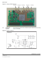
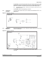
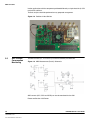
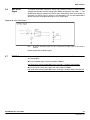
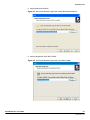
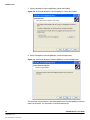
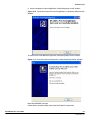
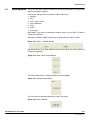
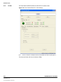
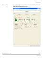
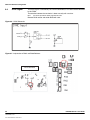
EV10AQ190x-DK VITA 57 FMC Quad 10-bit ADC Demo Kit EV10AQ190x-DK User Guide 1067BX–BDC–12/11 Table of Contents Section 1 General Overview ................................................................................. 1-1 1.1 1.2 1.3 Disclaimer .................................................................................................1-1 Quad 10-bit ADC.......................................................................................1-2 Demo Kit ...................................................................................................1-3 Section 2 Quick Start ............................................................................................ 2-1 2.1 2.2 Operating Procedure.................................................................................2-1 Troubleshooting ........................................................................................2-1 2.2.1 Installation ..........................................................................................2-1 2.2.2 Start up Procedure .............................................................................2-2 2.2.3 Measurement......................................................................................2-2 2.3 External Equipment...................................................................................2-6 Section 3 Main Functions ..................................................................................... 3-1 3.1 Analog Input Signal...................................................................................3-1 3.1.1 Analog Input Channel A......................................................................3-2 3.1.2 Analog Input Channel B......................................................................3-3 3.1.3 Analog Input Channel C .....................................................................3-3 3.1.4 Analog Input Channel D .....................................................................3-4 3.2 3.3 3.4 3.5 3.6 3.7 ADC Clock Input Signal ............................................................................3-4 Control of ADC Settings ............................................................................3-5 ADC Junction Temperature Monitoring.....................................................3-5 ADC Current Consumption Monitoring .....................................................3-6 ADC SYNC Signal ....................................................................................3-7 DC/DC Converter ......................................................................................3-7 Section 4 Software Tools...................................................................................... 4-1 4.1 4.2 4.3 4.4 4.5 EV10AQ190x-DK - User Guide Overview ...................................................................................................4-1 Configuration.............................................................................................4-2 User Interface Installation .........................................................................4-2 USB Driver Installation ..............................................................................4-8 Operating Modes ....................................................................................4-13 4.5.1 Settings.............................................................................................4-15 4.5.2 TEST ................................................................................................4-19 i 1067BX–BDC–12/11 4.5.3 Input Impedance...............................................................................4-22 4.5.4 CLOCK .............................................................................................4-24 4.5.5 Power ...............................................................................................4-25 4.5.6 Acquisition Control............................................................................4-26 4.5.7 Acquisition ........................................................................................4-28 4.5.8 Demo Kit Configuration File..............................................................4-34 4.5.9 Data Save File ..................................................................................4-35 4.5.10 Regional and Language Options ......................................................4-36 Section 5 FPGA CODE......................................................................................... 5-1 5.1 5.2 5.3 5.4 Software Configuration .............................................................................5-1 FPGA Binary File ......................................................................................5-1 FPGA Programming..................................................................................5-2 VHDL CODE .............................................................................................5-5 Section 6 Demo kit Hardware Configuration......................................................... 6-1 6.1 6.2 6.3 6.4 Channel D .................................................................................................6-1 Clock Selection .........................................................................................6-1 SPI Signal .................................................................................................6-2 SYNC Signal .............................................................................................6-4 Section 7 Layout Information ................................................................................ 7-1 Section 8 Mechanical Dimensions........................................................................ 8-1 Section 9 Ordering Information............................................................................. 9-1 ii 1067BX–BDC–12/11 e2v semiconductors SAS 2011 EV10AQ190x-DK - User Guide General Overview Section 1 General Overview The QUAD 10-bit Demo Kit enables the easy evaluation of the characteristics and performance of QUAD 10-bit ADC EV10AQ190x. The Demo kit is plug_and_play and needs little external equipment. The Demo kit is delivered with software which allows acquisition of data using the FPGA. The QUAD 10-bit Demo Kit is compatible with VITA57 FMC (FPGA Mezzanine Card) standard. For more information please see the VITA site web. http://www.vita.com/fmc.html The QUAD 10-bit Demo kit is 100% compatible with XILINX VIRTEX 6 evaluation kit ML605. This board is designed for use as a reference design. All front end devices are fitted including: DC-DC regulator, ADC driver, clock generator…. Please see Section 3 “Main Functions” . The FPGA VHDL data acquisition code for the ML605 board is supplied. Please see Section 5 “FPGA CODE” . 1.1 Disclaimer The information in this document is provided in connection with E2V products. No license, express or implied, by estoppel or otherwise, to any intellectual property right is granted by this document or in connection with the sale of E2V products. EXCEPT AS SET FORTH IN E2V'S TERMS AND CONDITIONS OF SALE LOCATED ON E2V'S WEB SITE, E2V ASSUMES NO LIABILITY WHATSOEVER AND DISCLAIMS ANY EXPRESS, IMPLIED OR STATUTORY WARRANTY RELATING TO ITS PRODUCTS INCLUDING, BUT NOT LIMITED TO, THE IMPLIED WARRANTY OF MERCHANTABILITY, FITNESS FOR A PARTICULAR PURPOSE, OR NONINFRINGEMENT. IN NO EVENT SHALL E2V BE LIABLE FOR ANY DIRECT, INDIRECT, CONSEQUENTIAL, PUNITIVE, SPECIAL OR INCIDENTAL DAMAGES (INCLUDING, WITHOUT LIMITATION, DAMAGES FOR LOSS OF PROFITS, BUSINESS INTERRUPTION, OR LOSS OF INFORMATION) ARISING OUT OF THE USE OR INABILITY TO USE THIS DOCUMENT, EVEN IF E2V HAS BEEN ADVISED OF THE POSSIBILITY OF SUCH DAMAGES. E2V makes no representations or warranties with respect to the accuracy or completeness of the contents of this document and reserves the right to make changes to specifications and product descriptions at any time without notice. E2V does not make any commitment to update the information. EV10AQ190x-DK - User Guide 1-1 1067BX–BDC–12/11 General Overview This kit must be regarded as a tool, not a finished product. It allows the evaluation of performance of the e2v component, design prototypes and debug software. It CANNOT be resold as a finished product that must be compliant with local relevant regulations. Its function is as a development system, demonstrating the performance of e2v semiconductors components and not as a final product available on general release. Since this Development Kit is intended to be used on an industrial workbench and modified by the user to build his prototypes, NO WARRANTY OF ANY KIND can apply. NO LIABILITY will be accepted by e2v, whatsoever may arise as a result of the use of these boards. All company and/or product names may be tradenames, trademarks and/or registered trademarks of the respective owner with which they are associated. 1.2 Quad 10-bit ADC The EV10AQ190x-DK Demo Kit is based on e2v EV10AQ190x 1.25 Gsps Quad 10-bit ADC whose block diagram is given on Section 1-1. Figure 1-1. EV10AQ190x Quad 10-bit ADC Block Diagram 2.5 GHz Clock Clock Buffer + selection + decimation + SDA LVDS Buffers LVDS Buffers LVDS Buffers 10 bit 1.25 Gsps ADC core 10 bit 1.25 Gsps ADC core 10 bit 1.25 Gsps ADC core Gain Gain T/H Phase Offset Serial Peripheral Interface Gain T/H 10 bit 1.25 Gsps ADC core Gain T/H Phase Offset LVDS Buffers Phase Offset T/H Phase Offset Analog MUX (Cross Point Switch) The EV10AQ190x Quad 10-bit ADC integrates four 10-bit ADC cores which can operate independently (four-channel mode) or group by two cores (two-channel mode with the ADCs interleaved two by two) or one-channel mode where all four ADCs are all interleaved. All four ADCs are clocked from the same external input clock signal and controlled via an SPI bus (Serial Peripheral Interface). An analog multiplexer (cross-point switch) is used to select the analog input depending on the mode the quad ADC is used. The clock input is common to all four ADCs. This block receives an external 2.5 GHz clock (maximum frequency) and generates the internal sampling clocks for each ADC core depending on the mode used. Please refer to latest version of datasheet EV10AQ190x for more information. http://www.e2v.com/products-and-services/specialist-semiconductors/broadband-dataconverters/datasheets/ 1-2 1067BX–BDC–12/11 e2v semiconductors SAS 2011 EV10AQ190x-DK - User Guide General Overview 1.3 Demo Kit Figure 1-2 provides an overview of system architecture. Figure 1-2. EV10AQ190x-DK Demo Kit System Architecture (when Connected with a VIRTEX6 Evaluation Kit) 12V supply adapter RF generator CLK DN D C B A PC GUI control, acquisition & analysis I/O USB control 4 channels e2v QUAD 10-bit VITA57 interface FPGA 12V supply adapter (VIRTEX 6) The complete system is built with the e2v demo kit and an FPGA development kit. e2v Demo kit contains the following items : Quad 10-bit Demo kit with EV10AQ190CTPY ADC Cables & Power Supply – Universal 12V power Adapter & Cables – USB Cables to communicate with a PC (control of ADC settings and settings for data acquisition) 4 analog inputs with SMA connectors 1 clock input with SMA connector (if external clock input is programming) 2 SAMTEC MC-HPC-8.5L connectors HPC (High Pin Count) compatible with VITA57 standard for ADC LVDS digital outputs CD ROM with GUI Software Note: EV10AQ190x-DK - User Guide The ML605 VIRTEX 6 Evaluation kit with XC6VVLX240T-1FFG1156 FPGA is not supplied within the e2v kit and should be purchased separately from Xilinx or its authorised distributors. 1-3 1067BX–BDC–12/11 General Overview Figure 1-3. EV10AQ190x-DK Demo Kit Simplified Schematic Figure 1-4. EV10AQ190x-DK Demo Kit Functional Architecture Device PC ADC Control & Events FPGA Acquisition & formatting Display Processing Acquisition FX2 USB Transport Layer USB cable Driver USB USB Transport Layer USB Acquisition and formatting of ADC digital output data are done within the FPGA Eval Kit. Data is then transmitted again to the ADC Demo Kit. A USB driver on the ADC Demo kit allows for transmission of the data to the computer that performs the display and processing of ADC output data (FFT). Software and Graphical User Interface are provided with the Demo Kit. The provided software operates using Labview RunTime (no license required). 1-4 1067BX–BDC–12/11 e2v semiconductors SAS 2011 EV10AQ190x-DK - User Guide Quick Start Section 2 Quick Start 2.1 Operating Procedure 1. Install the Software as described in section 4 Software Tools. 2. Install the FPGA code into ML605 Xilinx evaluation board (see Section 5.3 “FPGA Programming” ) 3. Turn OFF the ML605 Xilinx evaluation board. 4. Fix Heatsink/Fan to the ADC if no external form of ventilation is to be used (see Section 3.4) 5. Connect the QUAD 10-bit Demo Kit on ML605 Xilinx evaluation board. 6. Connect the power supplies of both evaluation boards. 7. Connect the USB cable. 8. Turn ON power supplies of QUAD 10-bit Demo Kit. 9. Turn ON power supplies of ML605 Xilinx evaluation board. 10. Launch the EvalkitQuadAdc10Bits.exe software. 11. Check if currents are correct (see Section 4.5.5 Power). 12. Select the ADC mode of your ADC (4 channels or 2 channels or 1 channel) 13. Turn the mode ADC test ramp active (see chap Section 4.5.2 TEST). This sequence is mandatory to allow the synchronization of 4 channels into FPGA 14. Launch acquisition and check if sample signal is correct. 15. Return to normal mode (Turn OFF Test mode). 16. Connect a RF generator on Analog input. 17. Turn on the RF generator. 18. Launch acquisition (see Section 4.5.7 Acquisition). 2.2 Troubleshooting 2.2.1 Installation Check that you own rights to write in the directory (administrator rights). Check for the available disk space. Check that the USB port is free and properly configured. – QUAD 10-bit connected to USB 2 driver EV10AQ190x-DK - User Guide 2-1 1067BX–BDC–12/11 Quick Start Figure 2-1. USB Port Driver Configuration Warning: this installation is done for one USB connector only. If USB connector is changed, USB driver need to be re-installed before use. 2.2.2 Start up Procedure Check that supplies are properly powered on and properly connected. Check if the Xilinx FPGA evaluation board ML605 is properly configured with correct software. Check if QUAD 10-bit Demo Kit is properly plugged into FPGA connector. Check if USB connector is properly plugged. 2.2.3 Measurement Check if QUAD 10-bit ADC is properly configured in normal mode without standby and test mode. Note: check if currents are correct (see Section 4.5.5 Power) Note: check if test mode is OFF (see Section 4.5.2 TEST) Check if acquisition mode is correctly configured. Warning: if no windowing is used or if signal is non coherent, FFT of Figure 6 is obtained 2-2 1067BX–BDC–12/11 e2v semiconductors SAS 2011 EV10AQ190x-DK - User Guide Quick Start Figure 2-2. FFT without Windowing or with non Coherent Signal Figure 2-3. FFT with Windowing Warning: if the Fin frequency has an exact value such as 250 MHz the FTT result is wrong that is why it is recommended to perform measurements with shift of few MHz e.g. 250.2 MHz. EV10AQ190x-DK - User Guide 2-3 1067BX–BDC–12/11 Quick Start Figure 2-4. Example of Wrong INL Measurement if Incorrect Fin such as Exactly 250 MHz With channel A and channel C (amplifier channels) an RF attenuator should be added on the SMA connecter to have optimum performance. When these channels are not being used the attenuator or 50 Ohm terminator should be kept in place. This will prevent the amplifiers from adding noise into the system. Figure 2-5. RF Attenuator Added on SMA Connector Check that the junction temperature of QUAD 10-bit ADC is lower than 105°C and that heatsink is properly connected. Figure 2-6. Junction Temperature Monitoring with GUII 2-4 1067BX–BDC–12/11 e2v semiconductors SAS 2011 EV10AQ190x-DK - User Guide Quick Start Check if acquisition is synchronous. The ADC RAMP test procedure will set the ADC to output a ramp on each channel these ramps are synchronous at the output of the ADC after a SYNC process has been completed. The FPGA RESET done during this procedure will always ensure that the 4 channels are acquired in the FPGA synchronously. However if the channels are found not to be synchronous as shown in Figure 2-7. Figure 2-7. Non Synchronous Channels Return to ADC test mode disable -> Apply and then return into ADC test mode ramp mode -> Apply. This will re-run the synchronization procedure of the ADC and FPGA.. Note: EV10AQ190x-DK - User Guide it is not always necessary to have the ramp patterns aligned to obtain correct data acquisition using the analog inputs. 2-5 1067BX–BDC–12/11 Quick Start Figure 2-8. Synchronous Channels Note: 2.3 External Equipment it is not always necessary to have the ramp patterns aligned to obtain correct data acquisition using the analog inputs. Even if the ramp mode is not synchronous, you could return to the normal mode and perform one acquisition. Normally the acquisition of sinus wave in normal mode is correct. The QUAD 10-bit Demo Kit needs very little external hardware. RF generator for Analog input signal – The QUAD 10-bit ADC can convert analog signals up to 2GHz – For optimum performance this generator must have a low phase noise Please see Table 2-1 for example of signal generator. Cables & Power Supply (provided by e2v) – Universal 12V power Adapter & Cables – USB Cables to communicate with a PC (control of ADC settings and settings for data acquisition) PC with Windows – Windows 2000/98/XP and Windows NT and Windows 7 (note 32bit only) Please see chap 4.1 Overview FPGA evaluation board compatible with VITA57 FMC standard – This Demo Kit board has been specially designed to be plugged with the XILINX VIRTEX 6 evaluation board EK-V6-ML605-G. The QUAD 10-bit Demo Kit could be used with other FPGA evaluation boards compatible with VITA57 FMC standard. However, an assessment of available connections should be made to ensure full compatibility. 2-6 1067BX–BDC–12/11 e2v semiconductors SAS 2011 EV10AQ190x-DK - User Guide Quick Start Option RF generator for clock input signal whose frequency is different than 2 GHz – The QUAD 10-bit Demo Kit provides clock signal at 2 GHz using its own PLL – The QUAD 10-bit Demo Kit could be tested with other clock frequency Please see Section 6.2 Clock selection Table 2-1. Example of RF Generator EV10AQ190x-DK - User Guide Signal Generator SSB Phase Noise @ 1 GHz (20 KHz Offset) Agilent E4424B 250KHz 2GHz (High spectral purity) < -134dBc/Hz Agilent E4426B 250KHz 4GHz (High spectral purity) < -134dBc/Hz SMA100A 9 KHz 6GHz (High spectral purity) < -140dBc/Hz 2-7 1067BX–BDC–12/11 Quick Start 2-8 1067BX–BDC–12/11 e2v semiconductors SAS 2011 EV10AQ190x-DK - User Guide Main Functions Section 3 Main Functions 3.1 Analog Input Signal The user only needs to provide an analog signal at the input. This signal is digitized by the ADC depending on the chosen operating mode: 4 channel mode (1 channel per ADC core) 2 channel mode (2 interleaved ADC cores) 1 channel mode (4 interleaved ADC cores) Each channel input is driven in different ways on the board: Single to Differential Amplifier from Analog Devices (A channel: ADA4960 D.C. coupled) Single to Differential Balun RF transformer (B channel:MACOM ETC1-1-13) Single to Differential Amplifier from Analog Devices (C channel: ADA4960- AC coupled) Direct input via SMA connector (D channel) (free for customer use) EV10AQ190x-DK - User Guide 3-1 1067BX–BDC–12/11 Main Functions Figure 3-1. Analog Input SMA Configuration A channel 3.1.1 Analog Input Channel A B channel C channel D channel Ext Clock The Analog input channel A uses a differential amplifier (ADC driver) from Analog Devices ref: ADA4960. Figure 3-2. Channel A : Schematic 3-2 1067BX–BDC–12/11 e2v semiconductors SAS 2011 EV10AQ190x-DK - User Guide Main Functions The ADA4960 is used in DC configuration with output common mode driven by ADC QUAD 10-bit. The input is biased at 2.5V since this is a requirement for best performance from the amplifier, this should be taken into account when using this input. Note: be careful that if a DC voltage is added after the RF generator output that this will not damage the generator. The ADA4960 is used in AC configuration in channel C. 3.1.2 Analog Input Channel B The Analog input channel B uses an RF Transformer from MACOM ref: ETC1-1-13 / MABA-007159 Figure 3-3. Channel B : Schematic 3.1.3 Analog Input Channel C The Analog input channel C uses a differential amplifier (ADC driver) from Analog Devices: ref: ADA4960-1. Figure 3-4. Channel C : Schematic The ADA4960-1 is used in AC configuration with output common mode driven by Quad 10-bit ADC. EV10AQ190x-DK - User Guide 3-3 1067BX–BDC–12/11 Main Functions 3.1.4 Analog Input Channel D This channel is free for customer use in differential and AC coupling configuration. Figure 3-5. Channel D : Schematic This Channel D could be used in DC configuration. Please see Section 6.1Channel D. 3.2 ADC Clock Input Signal ADC clock input is generated by Clock generated PLL Hititte HMC831 (on-board) at 2.0 GHz. This frequency is fixed. Figure 3-6. ADC Clock Input : Schematic Note: By default, the on-board PLL clock is selected but an external clock input (provided by a RF generator) is allowed. The clock signal is fed to the board via an SMA connector followed by Single to Differential Balun RF transformer (MABA-007159 MACOM). Note: for operation at different clock frequencies it is probable that the FPGA interface will need to be re-compiled using different timing constraints. Please see Section 6.2 Clock selection. 3-4 1067BX–BDC–12/11 e2v semiconductors SAS 2011 EV10AQ190x-DK - User Guide Main Functions 3.3 Control of ADC Settings The Graphical User Interface allows for complete monitoring and control of all the settings of EV10AQ190x Quad 10-bit ADC such as channel selection, Gain, Offset, Phase, test mode (with SPI signal). Please see Section 4.5 Operating Modes. Please refer to datasheet EV10AQ190x for more information. http://www.e2v.com/products-and-services/specialist-semiconductors/broadband-dataconverters/datasheets/ By default the SPI signal is controlled by FX2 microcontroller but it could be driven by the FPGA. Please refer to Section 6.3 SPI Signal for more information. 3.4 ADC Junction Temperature Monitoring ADC junction temperature can be monitored by a temperature sensor from ON Semiconductors Ref: ADM1032 http://www.onsemi.com/PowerSolutions/product.do?id=ADM1032 Figure 3-7. Temperature Sense: Schematic ADC junction temperature can be displayed on the PC via the GUI with a resolution of ±2°C. Please see Section 4.5.5 Power. In case of excessive junction temperature, the ADC power supply will be turned OFF and a message will notify the user via the GUI. The Demo Kit provides an external heat sink with internal fan This heat sink should be fixed to the Quad 10-bit ADC with a thermal conductive foil both side adhesive. If no other form of ventilation or cooling is to be employed the heatsink ventilator should be fixed to the ADC using the attachment pad provided and the cable should be connected to the connector as shown below. Note that because of the location of the component underneath the board a heatsink/fan is necessary. Alternatively an airflow across the component can have sufficient cooling effect. EV10AQ190x-DK - User Guide 3-5 1067BX–BDC–12/11 Main Functions In other applications with the component positioned differently a simple heatsink (4°C/W max) will be sufficient. Thermal analysis should be performed on any proposed arrangement. Figure 3-8. Position of Heat Sink/fan 3.5 ADC Current Consumption Monitoring The ADC currents (ICC, ICCO and ICCD) can be measured by the Demo Kit. Figure 3-9. ADC Measurement (Partial): Schematic ADC currents (ICC, ICCO and ICCD) can also be monitored via the GUI. Please see Section 4.5.5 Power. 3-6 1067BX–BDC–12/11 e2v semiconductors SAS 2011 EV10AQ190x-DK - User Guide Main Functions 3.6 ADC SYNC Signal The QUAD 10-bit ADC requires a SYNC signal when the internal configuration is changed (for example Channel configuration, DMUX configuration, test mode ….). The QUAD 10-bit Demo Kit performs this SYNC signal automatically when these modes are changed. The SYNC signal is driven by microcontroller FX2 and the D950LV0011 devices transform the single ended signal into an LVDS signal. Figure 3-10. ADC SYNC Signal Note: By default, the SYNC signal via FX2 is selected but a SYNC signal via the FPGA is allowed. Please see Section 6.4 SYNC Signal. 3.7 DC/DC Converter The power supply for the QUAD 10-bit Demo Kit is provided by DC/DC block from Linear Technologies. Vcc (3V3) power supply with micro module LTM8023 http://www.linear.com/pc/productDetail.jsp?navId=H0,C1,C1003,C1424,P39569 Vcco and Vccd (1.8V) power supply with micro module LTM8021 http://www.linear.com/pc/productDetail.jsp?navId=H0,C1,C1003,C1042,C1424,P81177 EV10AQ190x-DK - User Guide 3-7 1067BX–BDC–12/11 Main Functions Figure 3-11. 3V3A Power Supplies Figure 3-12. 1.8V Power Supplies The amplifier and PLL power supply uses low noise LDO regulators from Linear Technology. LT3029EDE 3-8 1067BX–BDC–12/11 e2v semiconductors SAS 2011 EV10AQ190x-DK - User Guide Main Functions Figure 3-13. EV10AQ190x-DK - User Guide 3-9 1067BX–BDC–12/11 Main Functions 3-10 1067BX–BDC–12/11 e2v semiconductors SAS 2011 EV10AQ190x-DK - User Guide Software Tools Section 4 Software Tools 4.1 Overview The Demo Kit board needs three different kinds of software tools: FPGA software The Demo Kit board can be plugged with XILINX VIRTEX 6 evaluation board EK-V6ML605-G http://www.xilinx.com/products/devkits/EK-V6-ML605-G.htm e2v provides FPGA program to be used with Quad 10-bit Demo Kit. User Interface software The User Interface software is a Visual C++ compiled graphical interface that does not require a licence to run on a Windows NT or Windows 2000/98/XP PC and windows7 (32 bit) The software uses intuitive push-buttons and pop-up menus to write data from the hardware. Display Software The User Display software is Labview software that does not require a licence to run on a Windows NT or Windows 2000/98/XP PC and Windows 7 (32bit) The software uses intuitive push-buttons and pop-up menus to write data from the hardware. Warning: For the software installation, administrative rights are needed. Warning: If the software is already installed a window appears. Figure 4-1. Error Message if Labview Software is Already Installed This applies when a previous version of software is present or a version of the Quad8 bit demo is present. When updating an installation it is recommended to uninstall the existing version (but not DK_DBC_Processing&Display). If an other demo kit software, e.g. the DK-Quad8, is installed this can be left in place. Click on OK and continue. EV10AQ190x-DK - User Guide 4-1 1067BX–BDC–12/11 Software Tools 4.2 Configuration The advised configuration for Windows 2000/98/XP and Windows NT is: "PC with Intel Pentium Microprocessor of over 100 MHz; "Memory of at least 24 Mo. For other versions of Windows OS, use the recommended configuration from Microsoft. 4.3 User Interface Installation 1. Install the Quad 10-bit Demo Kit application on your computer by launching the SetupEvalkitQuadAdc10Bits.exe installer (please refer to the latest version available). The screen shown in Figure 4-2 is displayed: Figure 4-2. Quad 10-bit Demo Kit Application "Setup Wizard" Window 4-2 1067BX–BDC–12/11 e2v semiconductors SAS 2011 EV10AQ190x-DK - User Guide Software Tools 2. Select Destination Directory Figure 4-3. Quad 10-bit Demo Kit Application "Select Destination Directory" 3. Select Components (Start Menu Folder) Figure 4-4. Quad 10-bit Demo Kit Application "Start Menu Folder" EV10AQ190x-DK - User Guide 4-3 1067BX–BDC–12/11 Software Tools 4. Select Components (Additional Tasks) Figure 4-5. Quad 10-bit Demo Kit Application "Additional Tasks" 5. Select Components (Ready to Install) Figure 4-6. Quad 10-bit Demo Kit Application "Ready to Install" 4-4 1067BX–BDC–12/11 e2v semiconductors SAS 2011 EV10AQ190x-DK - User Guide Software Tools If you agree with the install configuration, press Install button. Now a new process of installation started Processing&Display for installing Labview RunTime (no license required. Please follow instructions. Warning: don't press finish button on "Completing Setup wizard" window. The screen shown in Figure 4-7 is displayed: 6. Select Components Processing&Display (installation Wizard) Figure 4-7. Quad 10-bit Demo Kit Processing&Display "Installation Wizard" EV10AQ190x-DK - User Guide 4-5 1067BX–BDC–12/11 Software Tools 7. Select Components Processing&Display (Destination Folder) Figure 4-8. Quad 10-bit Demo Kit Processing&Display "Destination Folder" 8. Select Components Processing&Display (Install the Application) Figure 4-9. Quad 10-bit Demo Kit Processing&Display "Install the Application" The installation of the software is now completed but the Processing&Display software need to be launched. This installation is launched automatically. 4-6 1067BX–BDC–12/11 e2v semiconductors SAS 2011 EV10AQ190x-DK - User Guide Software Tools 9. Select Components Processing&Display (Completing Setup wizard" window) Figure 4-10. Quad 10-bit Demo Kit Processing&Display "Completing Setup Wizard" Window" 10. Select Quad 10-bit Demo Kit application (Completing Setup wizard" window) Figure 4-11. Quad 10-bit Demo Kit Application "Completing Setup Wizard" Window" Note about README message. Please follow instruction before using Quad 10-bit Demo Kit application. EV10AQ190x-DK - User Guide 4-7 1067BX–BDC–12/11 Software Tools Figure 4-12. README Message For the bugs/limitation for Excel display, please see Section 4.5.10 Regional and Language Options. 4.4 USB Driver Installation After the installation, Quad 10-bit Demo Kit can be powered up and connected to PC with USB cable. At the first connection a USB driver installation will be launched. Warning: if the Demo Kit is connected to another USB connector this installation must be re-started. The installation is normally fully automatic. If it is not launched automatically, please proceed as described below: The window shown in Figure 4-13 will be displayed. Figure 4-13. Install Driver Software Please choose: Locate and install driver software (recommended) 4-8 1067BX–BDC–12/11 e2v semiconductors SAS 2011 EV10AQ190x-DK - User Guide Software Tools Figure 4-14. Allow Windows to Search Driver Please choose: Yes, always search online (recommended) Figure 4-15. Browse the Driver Software Please choose: Browse my computer for driver software (advanced) EV10AQ190x-DK - User Guide 4-9 1067BX–BDC–12/11 Software Tools Figure 4-16. Choose the Folder Select C:\Program Files\E2V\EvalkitQuadAdc10Bits Figure 4-17. Warning: Installation Please choose: Install the driver software anyway A Data transfer has been beginning please wait. 4-10 1067BX–BDC–12/11 e2v semiconductors SAS 2011 EV10AQ190x-DK - User Guide Software Tools Figure 4-18. END of New Driver Installation The new driver has been installed After the installation, the interface can be launched with the following file: C:\Program Files\E2V\EvalkitQuadAdc10Bits\EvalkitQuadAdc10Bits.bat EV10AQ190x-DK - User Guide 4-11 1067BX–BDC–12/11 Software Tools The window shown in Figure 4-19 will be displayed. Figure 4-19. User Interface Demo Kit 4-12 1067BX–BDC–12/11 e2v semiconductors SAS 2011 EV10AQ190x-DK - User Guide Software Tools 4.5 Operating Modes The Quad 10-bit ADC software included with the Demo Kit provides a Graphical User Interface to configure the ADC. Push buttons, popup menus and capture windows allows easy: 1. Settings; 2. Test; 3. Gain / Offset / Phase; 4. Input Impedance; 5. Clock; 6. Power; 7. Acquisition; With Setting, Test, Clock and Acquisition windows always click on "APPLY" button to validate any command. Clicking the "CANCEL" button will restore last settings sent with "APPLY" button. Figure 4-20. APPLY / CANCEL Buttons With Gain/Offset/Phase and INL windows always click on "Write" then "Send" buttons to validate any command. Figure 4-21. Write / Send / Cancel Buttons The Reset button allows re-configuring ADC to the Default Mode. Figure 4-22. Hardware Reset Button This user interface could be reduced using "Hide Tab", below. Figure 4-23. Hide Tab Button EV10AQ190x-DK - User Guide 4-13 1067BX–BDC–12/11 Software Tools Figure 4-24. Demo Kit User Interface with Hide Tab Configuration On the bottom corner the software displays information about software and hardware revision. ChipId: revision of Quad 10-bit ADC Device: revision of FX2 software FPGA: revision of VHDL code Figure 4-25. Software and Hardware Revision 4-14 1067BX–BDC–12/11 e2v semiconductors SAS 2011 EV10AQ190x-DK - User Guide Software Tools 4.5.1 Settings Figure 4-26. User Interface Demo Kit In this window, 5 functions are available: ADC mode: General Standby Synchronization Reset EV10AQ190x-DK - User Guide 4-15 1067BX–BDC–12/11 Software Tools ADC mode: 4-channels mode = the 4 ADCs work independently at Fclock/2 sampling rate (where Fclock is the external clock signal frequency). Figure 4-27. ADC Mode: 4-channels Mode 2-channels mode = the 4 ADCs are interleaved 2 by 2 (A & B, C & D), the sampling rate is equal to Fclock (where Fclock is the external clock signal frequency), the analog inputs can be applied to A or B and respectively C or D. Figure 4-28. ADC Mode: 2-channels Mode 1 channel mode = the 4 ADCs are all interleaved, the sampling rate is Fclock x 2 (where Fclock is the external clock signal frequency), the analogue input can be applied to either A, B, C or D channel. Note: 4-16 1067BX–BDC–12/11 e2v semiconductors SAS 2011 because of limitation of ML605 evaluation board (LVDS max 1GHz in speed grade -1) The capture of Quad 10-bit data is limited to 2 GSps. EV10AQ190x-DK - User Guide Software Tools Figure 4-29. ADC Mode: 1-channel Mode Simultaneous channel mode = the analog input signal of channel A or B or C or D is sent to the 4 ADCs work at the same clock (4 ADC with the same timing) with Fclock/2 sampling rate (where Fclock is the external clock signal frequency). Figure 4-30. ADC Mode: Simultaneous Sampling General setting: Output mode = Gray coding or Binary coding Bandwidth selection: Nominal give 1.5 GHz bandwidth at -3dB; Full gives 3.2GHz bandwidth at -3dB; EV10AQ190x-DK - User Guide 4-17 1067BX–BDC–12/11 Software Tools Standby setting: No standby = all channels are active (A: ON, B: ON, C: ON, D: ON); Partial standby = either A & B are in standby or C & D are in standby; Full standby = all 4 ADCs are in standby. Figure 4-31. Standby Configuration Synchronization: Synchronization: programs the number of clock cycles prior to output clock restart after SYNC reset Figure 4-32. Extraclock Configuration Reset: Synchronization: programs the number of clock cycles prior to output clock restart after SYNC reset; Figure 4-33. Hard Reset 4-18 1067BX–BDC–12/11 e2v semiconductors SAS 2011 EV10AQ190x-DK - User Guide Software Tools 4.5.2 TEST In this window, the test mode is available: A ramp test is generated within each ADC and output Figure 4-34. Test Ramp Test Mode Note: this mode allows synchronizing the 4 channels of ADC with the FPGA RESET. The synchronizing procedure can be initiated by checking the Disable button and then the Apply button : Then check the ADC and Ramp button and then Apply. Then retrun to normal operation by checking the Disable button and clicking on Apply. A flashing bit is generated with one bit at 1 within each ADC and output is following with ten bit at 0 (1 FF pattern every ten 00 patterns) or after every 11 or 15 zeros depending on the selection. Figure 4-35. Flashing Test Mode FPGA Test (for testing communication between Demo kit and FPGA) : ramp test EV10AQ190x-DK - User Guide 4-19 1067BX–BDC–12/11 Software Tools Figure 4-36. FPGA Test Mode Gain / Offset / Phase Figure 4-37. Gain / Offset / Phase Settings In this window, it is possible to adjust gain, offset and phase of the selected channel via the "channel select" button on the top left of the user interface. 4-20 1067BX–BDC–12/11 e2v semiconductors SAS 2011 EV10AQ190x-DK - User Guide Software Tools A LED shows if the channel is ON (active - green LED) or OFF (not active - red LED) and if the same channel is ready (ready to receive gain, offset or phase orders - green LED) or busy (not ready to receive new calibration orders - red LED). Figure 4-38. Channel Selection Once a channel has been selected, gain/offset/phase of this channel can be adjusted: you first need to enter the desired value for the gain/offset/phase thanks to the cursor; if you need to retrieve the old value of the gain/offset/phase click CANCEL; then you should WRITE this value to the internal registers by clicking on the WRITE button, if several adjustments are needed (gain AND offset AND phase), then select each value and then click on the respective WRITE buttons; once all adjustments are made via the WRITE buttons, orders to the ADC SPI can be sent using the SEND button; the calibration is successful if the internal gain/offset/phase boxes display the entered values. If a new value for the gain/offset/phase has been entered by mistake, it is possible to retrieve the initial value by pushing the CANCEL button. Figure 4-39. Cancel Button In the following example, it can be seen that the internal Gain register is set to 0.059 and that the user wants the phase to be set to -15. In the second picture, the WRITE and SEND buttons have been pushed and the internal register shows the new entered value for the phase. EV10AQ190x-DK - User Guide 4-21 1067BX–BDC–12/11 Software Tools Figure 4-40. Gain Write Send Sequence 4.5.3 Input Impedance 4-22 1067BX–BDC–12/11 e2v semiconductors SAS 2011 Figure 4-41. User Interface Demo Kit - Input Impedance Settings EV10AQ190x-DK - User Guide Software Tools In this window, it is possible to re-adjust the internal input resistor, which should be matched to 50. The procedure is similar to the previous ones: select the channel where you need to adjust the input impedance check that the channel is ON and READY (green LEDs) enter the resistor value push the WRITE button to write these values to the internal registers (you can retrieve the initial value of the impedance by clicking on the CANCEL button) Figure 4-42. Input Impedance Write Sequence This function helps to re-adjust the input impedance in case of a slight mismatch due to temperature variations or process variations. EV10AQ190x-DK - User Guide 4-23 1067BX–BDC–12/11 Software Tools 4.5.4 CLOCK This sheet allows selection between the Internal PLL or external clock. Figure 4-43. User Interface Demo Kit - Clock Settings Note: because of limitation of ML605 evaluation board (LVDS max 1GHz in speed grade -1). The capture of Quad 10-bit data is limited to 2 GSps. 4-24 1067BX–BDC–12/11 e2v semiconductors SAS 2011 EV10AQ190x-DK - User Guide Software Tools 4.5.5 Power This sheet allows measurement of the Quad 10-bit power consumption and the internal junction temperature. Figure 4-44. User Interface Demo Kit - Power EV10AQ190x-DK - User Guide 4-25 1067BX–BDC–12/11 Software Tools 4.5.6 Acquisition Control This sheet controls the acquisition modes of the Quad 10-bit. Figure 4-45. User Interface Demo Kit - Acquisition Control 4-26 1067BX–BDC–12/11 e2v semiconductors SAS 2011 EV10AQ190x-DK - User Guide Software Tools Sampling Nbr: Number of samples in acquisition Must be a 2n For FFT N=4X2n (n=number bit of ADC). For INL N=16X2n (n=number bit of ADC) Example for 10-bit ADC FFT must be computed with 4096 points and INL with 16384 points Nb Harmonics: Number of Harmonics considered for THD and SNR calculation (Default value is 10 harmonics). FFT window: When the analog input signal and the sampling clock are not coherent signals, a FFT windows has to be applied to obtain a correct result. Analog Input Frequency: For use when the analog input is not the highest amplitude. Normally the systems takes the highest harmonic as H1. Bypass Interlacing This can be used in 1 or 2 channel modes for viewing the non-interlaced data. Peak width: When FFT windows is applied the Harmonic signal is composed of several points (Default value is 11). Figure 4-46. FFT Window Configuration Data can be saved in Excel file Figure 4-47. Save Data Configuration EV10AQ190x-DK - User Guide 4-27 1067BX–BDC–12/11 Software Tools Select directory Figure 4-48. Directory Selection Note: 4.5.7 Acquisition A manual operation is needed to name and save the file. The stream function can be used to start an acquisition Snap: for single acquisition Start for continuous acquisition, (stop acquisition with the stop button) Figure 4-49. User Interface Demo Kit - Stream Function When an acquisition is launched several window results appear: CH_A => ADC channel A CH_B => ADC channel B CH_C => ADC channel C CH_D => ADC channel D 4-28 1067BX–BDC–12/11 e2v semiconductors SAS 2011 EV10AQ190x-DK - User Guide Software Tools Figure 4-50. Sample Signal: Example of Signal in Simultaneous Channel Figure 4-51. INL Curve Example EV10AQ190x-DK - User Guide 4-29 1067BX–BDC–12/11 Software Tools Figure 4-52. FFT Spectrum Example Figure 4-53. FFT Parameters Example 4-30 1067BX–BDC–12/11 e2v semiconductors SAS 2011 EV10AQ190x-DK - User Guide Software Tools Plot selection: one channel or several channels can be plotted for easier reading. Figure 4-54. Plot Selection Figure 4-55. Zoom Selection: Several Kinds of Zoom can be chosen Figure 4-56. Lock Selection EV10AQ190x-DK - User Guide 4-31 1067BX–BDC–12/11 Software Tools Figure 4-57. Cursor Selection: and Move Cursor on Channel FFT parameters: this channel selection has to be used to see FFT parameters of several channels Selection 0 => ADC Channel A Selection 1 => ADC Channel B Selection 2 => ADC Channel C Selection 3 => ADC Channel D Figure 4-58. FFF Selection 4-32 1067BX–BDC–12/11 e2v semiconductors SAS 2011 EV10AQ190x-DK - User Guide Software Tools FFT Processing: For future calculations, we define: N Sig = Signal power level = ""spectrumi 2 0 setup.PeakWidth Ho = Power of the continuous component = spectrum i 2 0 setup.PeakWidth H1 = Power of the fundamental = spectrumi 2 j setup.cal..Nbr of Harmonics ""setup.PeakWidth Harmonics j Hi = Power of the harmonics = spectrum i 2 with: setup_PeakWidth = 1 = width of one spur given in number of points; setup_cal_NbrOfHarmonics = 5 or 10 = number of harmonics used for the spectral calculations PmaxSpur = Power of the highest spur excluding the continuous component and the fundamental setup.PeakWidth = spectrum i 2 j SFSR dBc = H1 dB Average Noise rms = Sig – H0 – H1 --------------------------------------------N sig – N H0 – N H1 N = number of points H1i THD dBc = 10 log --------H1 H1 SNR dBc = 10 log --------------------------------------------------Sig – H0 – H1 – H1i Harmonic rms SFDR dBc = 20 log -----------------------------------------fundamental rms 2 Sig – H0 – Average Noise rms SINAD dBc = 10 log -------------------------------------------------------------------------------Sig – H0 – H1 SINAD dB – 10 log 1.5 ENOB = --------------------------------------------------------6.02 THD dBFS = THD dBc + SFSR dBc SNR dBFS = SNR dBc – SFSR dBc SFDR dBFS = SFDR dBc + SFSR dBc EV10AQ190x-DK - User Guide 4-33 1067BX–BDC–12/11 Software Tools SINAD dBFS = -10 log 10 (-SNR dBFS/ /10) + 10 (THD dBFS/ /10) SINAD dBFS – 10 log 1.5 ENOB dBFS = --------------------------------------------------------------6.02 The parameters with the _FS prefix correspond to the same parameter but in dBFS (from full scale). 4.5.8 Demo Kit Configuration File It is possible to save the context of the Demo Kit (saving of all settings and configuration). This context can be saved for later use, so that saved settings can be reloaded. File DK BDC QUAD10bit Conf.ctx Figure 4-59. Example of Context of the Demo Kit Warning: for each channel A B C D don't forget to push the SEND button to perform this setting on each sheet (Setting, Gain/Offset/Phase, INL…). 4-34 1067BX–BDC–12/11 e2v semiconductors SAS 2011 EV10AQ190x-DK - User Guide Software Tools 4.5.9 Data Save File It is also possible to save the data of your acquisition (saving of all data samples and FFT result). This data is stored into an Excel file with different sheet: Sample signal: Data of Quad 10-bit ADC with channel A B C D in this order in columns INL curve of channel A B C D in this order in columns FTT parameters (SFDR, THD, SNR, SINAD, EBOB) of each Channel A B C D in line Harmonic level of each channel A B C D in columns FFT Module and FFT frequency of each Channel A B C D in columns File: DK BDC QUAD10bit DATA.xls Figure 4-60. Example of Excel File Column A: corresponds to channel A Column B: corresponds to channel B Column C: corresponds to channel C Column D: corresponds to channel D Warning: before using, your PC needs to be configured. The decimal separator must be a dot "." instead of comma "," like in French. Use a control Regional Setting to check if decimal separator is configured with a dot ".". EV10AQ190x-DK - User Guide 4-35 1067BX–BDC–12/11 Software Tools 4.5.10 Regional and Language Options Use a control Regional Setting to check if decimal separator is configured with a dot ".". Figure 4-61. Regional and Language Options 4-36 1067BX–BDC–12/11 e2v semiconductors SAS 2011 EV10AQ190x-DK - User Guide Software Tools Selection: Customize this format. Figure 4-62. Customize Regional Option Sheet Numbers The decimal separator must be configured with a dot "." EV10AQ190x-DK - User Guide 4-37 1067BX–BDC–12/11 Software Tools 4-38 1067BX–BDC–12/11 e2v semiconductors SAS 2011 EV10AQ190x-DK - User Guide FPGA CODE Section 5 FPGA CODE The FPGA code has been designed to be used with ML605 Xilinx Virtex 6 evaluation board. Figure 5-1. ML605 Xilinx® VIRTEX® 6 Evaluation Board Warning: Please configure your ML605 evaluation board with correct Switch configuration. 5.1 Software Configuration 5.2 FPGA Binary File A binary file is provided with the Demo Kit XILINX configuration: VIRTEX-6 FPGA ML605 Evaluation Kit Xilinx ISE Design Suite version 12 or upper with IMPACT software CDROM\FPGA Bin\quad10_demo_v1.1.bit – Configuration PLL at 2 GHz with data rate into FPGA at 1Gbps Note: because of limitation of ML605 evaluation board (LVDS max 1Gb/s in speed grade -1) The capture of Quad 10-bit data in requires Fclock lower than 2 GHz. Two Binaries are provided for iMPACT software CDROM\FPGA Bin\prog_q10.ipf (configuration of iMPACT) CDROM\FPGA Bin\prog_DKQ10_V1.1.mcs (PROM file) EV10AQ190x-DK - User Guide 5-1 1067BX–BDC–12/11 FPGA CODE 5.3 FPGA Programming Connect the USB Mini cable on USB JTAG connector J22 Change the Configuration Mode Switch and System ACE Address Figure 5-2. Configuration Mode Switch of ML 605 Board Launch the iMPACT of ISE suite and load the CDROM\FPGA bin\bin\prog_q10.ipf Figure 5-3. Loading of DKQUAD10bit.ipf file Note: ensure that program into PROM is correctly programmed. Don't forget to program the CDROM\FPGA Bin\progQ10_V1.1.mcs file into PROM. 5-2 1067BX–BDC–12/11 e2v semiconductors SAS 2011 EV10AQ190x-DK - User Guide FPGA CODE Figure 5-4. Programming the File PROM\DKQUAD10bit.mcs Figure 5-5. Program Succeeded EV10AQ190x-DK - User Guide 5-3 1067BX–BDC–12/11 FPGA CODE 5.4 VHDL CODE A documentation of VHDL architecture is provided with the Demo Kit. See CDROM\Documentation\FPGA Code\ DK_QUAD10_bits_FPGA_Design_Document_v1.pdf Figure 5-6. VHDL Top level simplified block diagram Register Bank Acquisition Manager 10 10 SERDES Sample Slip FIFO RAM SERDES Sample Slip FIFO RAM Sequencer 10 SERDES Sample Slip FIFO RAM 10 SERDES Sample Slip FIFO RAM 5-4 1067BX–BDC–12/11 e2v semiconductors SAS 2011 OUTPUT INTERFACE EV10AQ190x-DK - User Guide Demo kit Hardware Configuration Section 6 Demo kit Hardware Configuration The Demo Kit could be hardware configured by changing manually some capacitor or resistance. This chapter describes all user settable hardware configurations. 6.1 Channel D The Channel D could be used in DC configuration mode by replacing C126 and C127 by a 0 resistor. Figure 6-1. Channel D Schematic 6.2 Clock Selection The ADC clock is generated by a PLL, but an external clock can be used (for frequency different than PLL). The selection between the two clocks is done manually with a resistor. Remove R15 and R37 resistors and solder R36 and R50 with a 0. Note: EV10AQ190x-DK - User Guide The VHDL code supplied permits operation at 2 GHz. A re-compilation with different timing constraints will be required for other frequencies. 6-1 1067BX–BDC–12/11 Demo kit Hardware Configuration Figure 6-2. ADC Clock Selection Schematic Figure 6-3. Implantation of R15, R37, R36 and R50 Resistors TOP VIEW 6.3 SPI Signal The SPI signal is controlled by the FX2 microcontroller, but it could also be controlled by FPGA. The selection between the two clocks is done manually with a resistor. Note: e2v doesn't provide the SPI controller FPGA code. Remove R93, R95, R97, R99 and R101 resistors and solder R94, R96, R98, R100 and R102 with a 0. 6-2 1067BX–BDC–12/11 e2v semiconductors SAS 2011 EV10AQ190x-DK - User Guide Demo kit Hardware Configuration Figure 6-4. SPI Schematic Figure 6-5. Implantation of R93, R94, R95, R96, R97, R98, R99, R100, R101 and R102 resistors BOTTOM VIEW EV10AQ190x-DK - User Guide 6-3 1067BX–BDC–12/11 Demo kit Hardware Configuration 6.4 SYNC Signal The SYNC signal is controlled by the FX2 microcontroller, but it could also be controlled by the FPGA. The selection between the two clocks is done manually with a resistor. Note: e2v doesn't provide the SYNC signal FPGA code. Remove R105 resistor and solder R106 with a 0. Figure 6-6. SYNC Schematic Figure 6-7. Implantation of R105 and R106 Resistors BOTTOM VIEW 6-4 1067BX–BDC–12/11 e2v semiconductors SAS 2011 EV10AQ190x-DK - User Guide Layout Information Section 7 Layout Information Figure 7-1. Top Side Layer 1 Figure 7-2. Bottom Side Layer 12 EV10AQ190x-DK - User Guide 7-1 1067AX–BDC–06/11 Layout Information 7-2 1067AX–BDC–06/11 e2v semiconductors SAS 2011 EV10AQ190x-DK - User Guide Mechanical Dimensions Section 8 Mechanical Dimensions The Demo Kit board with Quad 10-bit ADC dimension is 139 mm × 76.5 mm × 8 mm. It is compatible with VITA57 FMC standard. Figure 8-1. Mechanical Dimensions EV10AQ190x-DK - User Guide 8-1 1067AX–BDC–06/11 Mechanical Dimensions 8-2 1067AX–BDC–06/11 e2v semiconductors SAS 2011 EV10AQ190x-DK - User Guide Ordering Information Section 9 Ordering Information Table 9-1. EV10AQ190x-DK - User Guide Ordering Information Part Number Temperature Comments EV10AQ190TPY-DK Ambient ROHS compliant 9-1 1067BX–BDC–12/11 Ordering Information 9-2 1067BX–BDC–12/11 e2v semiconductors SAS 2011 EV10AQ190x-DK - User Guide How to reach us Home page: www.e2v.com Sales offices: Europe Regional sales office Americas e2v ltd e2v inc 106 Waterhouse Lane 520 White Plains Road Chelmsford Essex CM1 2QU Suite 450 Tarrytown, NY 10591 England USA Tel: +44 (0)1245 493493 Tel: +1 (914) 592 6050 or 1-800-342-5338, Fax: +44 (0)1245 492492 Fax: +1 (914) 592-5148 mailto: [email protected] mailto: [email protected] e2v sas Asia Pacific 16 Burospace e2v ltd F-91572 Bièvres Cedex 11/F., France Onfem Tower, Tel: +33 (0) 16019 5500 29 Wyndham Street, Fax: +33 (0) 16019 5529 Central, Hong Kong mailto: [email protected] Tel: +852 3679 364 8/9 Fax: +852 3583 1084 e2v Aerospace and defense inc mailto: [email protected] 765 Sycamore Drive Milpitas California 95035 USA Tel: +33 (0) 1 408 737 0992 Fax: +33 (0) 1 408 736 8708 mailto: e2v-us.com Product Contact: e2v Avenue de Rochepleine BP 123 - 38521 Saint-Egrève Cedex France Tel: +33 (0)4 76 58 30 00 Hotline: mailto: [email protected] Whilst e2v has taken care to ensure the accuracy of the information contained herein it accepts no responsibility for the consequences of any use thereof and also reserves the right to change the specification of goods without notice. e2v accepts no liability beyond that set out in its standard conditions of sale in respect of infringement of third party patents arising from the use of tubes or other devices in accordance with information contained herein. e2v semiconductors SAS 2011 1067BX–BDC–12/11 1067BX–BDC–12/11 e2v semiconductors SAS 2011