1
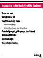
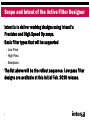
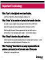
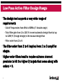
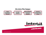
iSIM ACTIVE FILTER DESIGNER NEW, VERY CAPABLE, MULTI-STAGE ACTIVE FILTER DESIGN TOOL Michael Steffes Sr. Applications Manager 12/15/2010 SIMPLY SMARTER™ Introduction to the New Active Filter Designer • Scope and Intent • Getting into the tool • Two Primary Design Flows – Semi-automatic design – User specified poles and gains for each stage • From design targets, pick op amps, simulate, and save/share features. • Example Designs • Supporting Information 2 Scope and Intent of the Active Filter Designer • Intent is to deliver working designs using Intersil’s Precision and High Speed Op amps. • Basic filter types that will be supported – Low Pass – High Pass – Bandpass • The list above will be the rollout sequence. Low pass filter designs are available at this initial Feb. 2010 release. 3 Important Terminology • Filter “Type” is the highest level classification. – Low Pass, High Pass, Notch, Bandpass, Allpass, etc. • Filter “Order” is the number of poles in the transfer function – 1st order is just a single energy storage element (like an RC filter) – 2nd order stages are only complex poles in this tool (Q >0.5) – 2nd through 6th order filters supported by the tool (built up as a combination of 1st and 2nd order stages – no 3rd order stages) • Filter “Shape” describes the pole locations – Infinite number of possible combinations of multiple pole locations – some standard ones include Butterworth, Chebyshev, etc. • Filter “Topology” describes the op amp implementation to achieve a particular 1st or 2nd order set of filter poles – Sallen-Key is one popular one. 4 Low Pass Active Filter Design Range • The design tool supports a very wide range of requirements – Cuttoff frequencies from 5Hz to 50Mhz (7 decade range) – Total filter gain from 1 to 10V/V in semi-automatic design flow but up to 125V/V (3 stage design) in the manual design flow – Filter order from 2 to 6 • The filter order from 2 to 6 implies from 1 to 3 amplifier stages. • Higher order filters tend to require extreme element precision to hit the higher Q targets that come along with orders > 6. 5 Op Amp Model List with New MacroModels • Table of op amps in the Intersil Active Filter Designer – sorted by VFA then CFA and then by ascending GBP or BW (for CFA) as of Dec. 2010 6 Single Channel Part # Topology GBP/BWmax Nominal VFA/CFA MHz Total Vcc ISL28194 ISL28195 ISL28158 ISL28156 ISL28133 EL8176 ISL28107 ISL28117 ISL28113 ISL28136 ISL28114 ISL28127 ISL28110 ISL24021 ISL28191 ISL55001 ISL28190 EL8101 EL5103 EL5101 EL8103 EL5105 EL2126 EL2125 ISL55190 EL5131 EL5161 EL5163 EL8108 HFA1105 HFA1109 EL5165 EL5167 VFA VFA VFA VFA VFA VFA VFA VFA VFA VFA VFA VFA VFA VFA VFA VFA VFA VFA VFA VFA VFA VFA VFA VFA VFA VFA CFA CFA CFA CFA CFA CFA CFA 0.0035 0.01 0.2 0.25 0.4 0.4 1 1.5 2 5.1 7.7 10 12 15 61 68 83.3 106 165 170 198 264 500 700 700 900 95 140 190 270 340 370 620 5 5 5 5 5 5 30 30 5 5 5 30 30 10 5 30 5 5 10 10 5 10 30 30 5 10 10 10 12 10 10 10 10 Single Typ. Is Min Vcc Max Vcc Channel mA (at Vcc) Disable Version 0.00033 1.8 5.5 ISL28194 0.001 1.8 5.5 ISL28195 0.034 2.4 5.5 ISL28158 0.039 2.4 5.5 ISL28156 0.018 2 5.5 0.055 2.4 5.5 EL8176 0.21 4.5 40 0.44 4.5 40 0.09 1.8 5.5 0.9 2.4 5.5 ISL28136 0.4 1.8 5.5 2.2 4.5 40 2.6 9 40 2 4.5 19 2.6 3 5.5 ISL28191 9 8 30 ISL55002 8.5 3 5.5 ISL28190 2 3 5.5 EL8100 5 5 12.6 EL5102 2.5 5 12.6 EL5100 5.6 4 5.5 EL8102 5 5 12.6 EL5104 5 4 30 10.8 4 30 16 3 5.5 3.5 5 13 EL5130 0.75 5 12.6 EL5160 1.5 5 12.6 EL5162 14.3 4.5 13 5.8 9 11 HFA1145 9.6 9 11 5 5 12.6 EL5164 8.5 5 12.6 EL5166 Dual Versions ISL28258 ISL28256 ISL28233 ISL28276 ISL28207 ISL28217 ISL28213 ISL28236 ISL28214 ISL28227 ISL28210 Quad Versions ISL28433 ISL28476 ISL28413 ISL28414 ISL28291 ISL28290 EL8201 EL5203 EL5205 ISL55290 EL5261 EL5263 EL8108 EL8401 Feature set for the New/Upgraded Macromodels • Typical, room temp., nominal power supply voltages used to produce the following characteristics: • Open and closed loop I/O impedances • Open loop gain and phase • Closed loop bandwidth and frequency response peaking under different external conditions • Loading effects on closed loop frequency response • Input noise terms including 1/f effects • Slew rate • Input and Output Headroom limits to I/O voltage swing • Supply current at nominal specified supply voltages • Nominal input DC error terms (1/3 of specified data sheet test or specified limits – intended to give 1σ error term on one polarity) • Load current reflected into the power supply current 7 Features not supported by the Macromodels • Harmonic distortion effects • Composite video differential gain and phase errors • Output current limiting (if any) • Disable operation (if any) • Thermal effects and/or over temperature parameter variation • Limited performance variation vs. supply voltage modeled • Part to part performance variation due to normal process parameter spread • Any performance difference arising from different packaging • Multichannel device crosstalk effects 8 Enhanced Capability Provided by the Tool • Semi-automatic design flow for multi-stage filters – Spreads the gain (from 1 to 10V/V total) between the stages and sequences the poles (order >2) in a way that reduces non-linear effects. • Significantly improved circuit implementations. – Noise effects considered and reduced if possible – 2nd order issues in the feedback and gain setting elements considered (loading, noise, BW, phase margin) • Resistor solutions adjusted to account for amplifier bandwidth effects to hit the desired pole locations more precisely. This also allows reduced amplifier bandwidth vs. target Fo design margin than many currently available design tools. 9 Common Misconceptions about Active Filters • The Active Filter Designer includes numerous features that might appear to violate some widespread myths – – Current feedback amplifiers (CFA’s) cannot be used in active filters. • They are in fact very suitable as wideband gain blocks if that is what is needed in the filter stage. Cannot be used (easily) with reactive feedback type topologies such as the MFB (or infinite gain) circuit. – Gain of 1 is required for the active filters (or low gain) • The gain is a design variable and can be accounted for in setting the R’s and C’s. But it does interact strongly with the amplifier bandwidth if VFA devices are used – and this is also accounted for in the design algorithms provided in the tool. – Equal R or Equal C designs are required or desirable. • This comes from simplified academic developments or where the text is headed towards integrated solutions (close cap. ratio’s desirable for integrated filters). Not really a required constraint for discrete implementations. 10 Entry from the main Intersil Web site • Currently, the top listing under the Design Resources and Tools is the “iSim Online Design Simulation” • Clicking that, takes you to 11 Available Design Tools under iSim option (12/2010) • Currently, the iSim application tools are broken into Power and Op amps. The top selection in the op amps is this new design tool. • Clicking the Active Filter Designer takes you to 12 iSim Active Filter Designer 13 First Step in Getting to a Filter Implementation • Coming into the tool fresh will give you the first “Requirements” screen set up to a default condition. Hitting the drop down keys will show other options. 14 The Tool is Mainly an Implementation Aid. • Many vendor tools provide some filter shape help as an early step in their tools. This is used to arrive at a desired filter order and pole locations to hit a particular “skirt” shape (how fast the cutoff band rolls off). Usually this is specified in terms of stop band attenuation at a certain frequency above the desired passband. • The Active Filter Designer assumes you already know the target shape and/or the approximate order or filter poles you want to implement. • The tool mainly works on getting the right op amp selected and design implemented in a way the will yield a successful board level implementation. 15 The Tool is Mainly an Implementation Aid. • If you need help deciding on the filter shape, try this web site – (free download that has a lot of filter shape design tools – just need to get the pole locations from here, or the shape description, to use in the iSim Active Filter Designer) • Filter Wiz PRO • http://www.schematica.com/filter_wiz_files/FWPRO.htm • Exact pole locations and advanced features may require you to purchase the full version. 16 AC Response Preview • From whatever settings are used in the upper section of the “Requirements” screen, hitting “Update Preview” will generate the ideal Gain, Phase, and Group delay. These are used later to compare to the actual circuit level implementation. Here is the screen after hitting Update Preview. 17 Two Primary Flows through Active Filter Designer 1. Semi-Automatic flow is where you want to use some of the pre-loaded filter shapes and let the tool do most of the work for you. This is the default mode and is what is shown on first entering the tool. – This flow also decides for you the sequence of poles (order >2) and how to implement the total target gain. It is essentially sequencing from high to low Q stages in low to higher gains in those stages in going from input to output. 2. Manual Pole selection is where you have some specific pole locations you wish to implement and want to enter those directly. – This also allows you to select the Frequencies, Gains and Q’s over a wider range than the semi-automatic path. – This is all selected in the row that asks “Enter Poles Manually”. This defaults to “No”, but clicking “Yes” changes this screen to accept user entry for each stage. The order setting still sets the number of stages and an odd order (3 or 5) forces the real pole to be the last stage. 18 Manual Pole Entry Option • Here, the entry screen has been changed by clicking “Yes” on the “Enter Poles Manually?” line and we have changed the gain in each stage to 10 giving an overall filter gain of 100 (10 in each stage is the maximum for 2 stage designs) and manually set the Q’s to get a 4th order Butterworth shape then hit “Update Preview” again. Hitting the “Continue” key from here -> 19 Setting up the Design • Hitting “Continue” from the “Requirements” page will go the “Setup” page where numerous implementation parameters are considered and available for modification. This step starts out with some default assumptions. • This is where the real work begins in matching op amps to the desired filter implementations. • For multi-stage filters, the most important thing to notice on this next screen is which stage is “active” in the setup screen. This is the red color on the Stage # tab. It comes into this step with the last stage as the default “active” stage. This is where the design constraints can be updated. Those also default to the values shown on the next slide, but can be modified. 20 Setting up the Design • The main goal for this step is to pick the right op amps for each stage given the topology, filter targets, and constraints. 21 21 Setting up the Design • The 2nd most important thing is that the “Constraints” can only be changed if you sitting on the final stage as the “active” stage. This is mainly related to the final output Vpp target. That can be updated for the last stage, but is then calculated for all previous stages and hence cannot be updated if you are sitting on those earlier stages for amplifier selection purposes. • While sitting on each “stage” tab, the tool is computing and reporting the implied requirements for that stage. These include – Bandwidth if the stage is non-inverting. Since this can be either a VFA or CFA op amp, gain bandwidth is not used in this line. So, taking the required BW number times the stage gain will give you the required GainBandwidth Product if you want to use a VFA op amp in this stage. – If you change the stage to be inverting, only VFA devices can be used and this computation reports the required Gain Bandwidth Product (GBP) 22 Adjustments Available on the Setup stage • On any given stage, you can change the topology from noninverting (default) to inverting and that immediately updates the recommended amplifier list at the bottom (this is the only thing that can be changed when you are sitting on earlier stages) • Sitting on the last stage, you can change the following global constraints – – Desired total supply voltage (range here is 1.8V to 40V). This supply voltage is assumed to be the same for all stages. – Maximum final stage Output Swing Vpp (limited to be from 10% to 90% of Vs) – Linearity Target – either SFDR if frequency domain or Step if step response • If SFDR, also asks for maximum expected frequency and desired distortion range – Resistor tolerance (exact, 0.5%, 1%, or 2%) • This effects the filter accuracy in that exact R solutions might be snapped to available values probably shifting the achieved filter shape off somewhat 23 Adjustments Available on the Setup stage • Several of these constraints are feeding into the “Estimated minimum slew rate required” reported on each stage. – Slew rate is estimated to achieve either an SFDR target or step response without slew limiting. The SFDR constraint is a necessary but not sufficient condition to achieve a certain distortion level – you might still not get the SFDR with a device offering the reported slew rate, but you reduce your chances if the device does not have at least the reported slew rate for that stage. – For a step response, the tool is looking at the pole locations of that stage and the desired nominal Vopp or Vstep at the output. It then computes the peak dV/dT to produce that output from an ideal input step and takes 2X that number for a design target. – Possible op amps to use in each stage use this Slew Rate calculation to constrain the list to op amps that offer at least 90% of this calculated value. 24 Picking Suitable Op Amp Solutions • The goal of this “Setup” page is to pick a suitable op amp that will work in each stage in the design. – If possible, the tool will automatically pick the closest fit as you come into this step, but that can be overridden by picking one of the parts listed at the bottom of the screen. Selecting on the “red” part number will take you to the product page for that device – showing package styles/pricing/availability/etc. • These are often different devices auto-filled in each stage, but these can often be made the same device with a little effort. • Changing the supply voltage will typically show a completely different set of op amps. • For instance, going to 10V total supply with 6Vpp output will show the following screen. (hit the “Apply” key after you update the supply voltage and output swing fields) 25 Modifying the Constraints gives new part choices • More CFA parts show up here as the prior setting of 5V supply and 2Vpp output violated the 1.6V headroom on those CFA parts 26 Picking Suitable Op Amp Solutions • The part choices are sorted by minimally acceptable to increasing design margin to the requirements. The top device in the table generated for each stage is deemed minimally suitable and is the default part filled into the top boxes. Going down the list gives more design margin. • This step requires a device selection for each stage before the next step (hitting “Design”) • At any time, you can change a stage to inverting, which then constrains the solution op amps to be VFA since CFA devices cannot (easily) be applied to the those topologies. • The Setup and design process works in gain “magnitudes” but it does report if the overall filter is inverting or non-inverting. 27 Picking Suitable Op Amp Solutions • To summarize, the computed minimum requirements for each stage shown on this screen include – Bandwidth if the stage in non-inverting, Gain Bandwidth Product if inverting – Slew rate – Maximum Vopp including any step overshoot or frequency response peaking – Maximum input Vipp. • These terms are used to constrain and sort the table of op amp selections to parts that – – Can operate at the specified total supply voltage – Will not clip given that supply voltage and output swing (including any peaking or step overshoot effects) considering the output headroom of each device. – Provides at least 90% of the computed minimum BW and slew rate. – Will not limit on the input given the supply voltage and input headroom limits of each device considered. 28 Executing the Design • Once we have design targets for each stage and an op amp selected, hitting the “Design” key will go off and compute the R’s and C’s for each stage and come back with a completed design. • At that point the total specified supply is split into +/(Vs/2) halves and the design is shown as a DC coupled, ground centered, signal swing implementation. • Hitting “Design” from the previous screen (10V supply, 6V output swing), gives the following active filter design. 29 Example Design Output Page • Note the multi-channel versions at the bottom and the simulation options at the top – Hitting the AC tab will run an AC simulation 30 Output of the AC simulation key. • Clicking on the Filter AC Output opens a waveform viewer where we can add the Ideal Gain, Phase, and Group Delay. Doing that - 31 Comparison of Actual to Ideal AC Response. • This viewer also has two cursors that can be moved and a zoom in feature. Here we see very good overall fit for the simulated filter response vs. ideal. Note the 40dB gain at low frequencies. 32 Design Summary and Saving/Sharing Options • Going back to the Filter tool (from the waveform viewer) and clicking Design Summary, will give the following screen 33 Design Summary and Saving/Sharing Options • This summarizes the overall targets, the constraints, and the final circuit design. • Down below on this screen are the BOM the AC, Transient, and/or noise sims that have been done. • Most importantly, in the upper right are 3 paths to go on from here – – Save the design (the little floppy icon). This saves the design locally in your filter tool folder so you open it up and work on it later. Once saved, you can also share the design by emailing it from the “Saved Designs” tab. – Download to PDF. This takes the design summary and creates a pdf version that can be saved (and then easily emailed around to colleagues/customers) – Download to iSim PE. This ports the schematic into a more general purpose simulator where added operations can be performed. These include MonteCarlo simulations, re-ordering the stages, converting it to a single supply design, etc. 34 Added Information and Filter Tool Extensions • Full User’s manual added March, 2010. “Designer’s Manual for the iSim Active Filter Designer” – AN1548 • Additional parts will be easily added to the tool as they become available (new parts) or as needed (older parts not currently included). Last update in Nov. 2010. • Op Amps in the tool have totally updated/upgraded Spice Macromodels. • Next addition will be the High Pass Filter flow, followed by the BandPass Filter flow during 2011. • If you use the tool and find an issue, please try to re-create it keeping track of exactly how you got to that point and report it using the Feedback option. It is also helpful to save the design and share it. 35