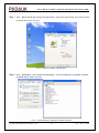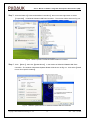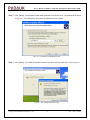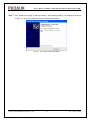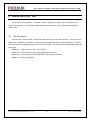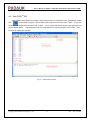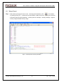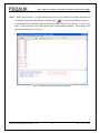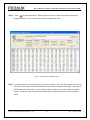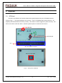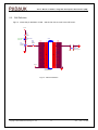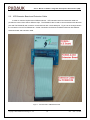
1
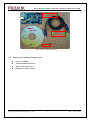
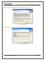
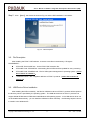
PADAUK FPPA™ IDE User ’s Manual Preliminary Version 0.40 – Dec. 28, 2006 C C P A D A U K T C Cooopppyyyrrriiiggghhhttt ©222000000555 bbbyyy P PA AD DA AU UK KT Teeeccchhhnnnooolllooogggyyy C Cooo...,,, LLLtttddd...,,, aaallllll rrriiiggghhhttt rrreeessseeerrrvvveeeddd 10F-2, No. 1, Sec. 2, Dong-Da Road, Hsin-Chu 300, Taiwan, R.O.C. TEL: 886-3-532-7598 + www.padauk.com.tw User’s Manual of FPPA™ Integrated Development Environment (IDE) Important Notice PADAUK Technology Co., Ltd.(PADAUK Technology)reserves the right to change this documentation without prior notice. Information provided by PADAUK Technology is believed to be accurate and reliable. However, PADAUK Technology makes no warranty for any errors which may appear in this document. Please contact PADAUK Technology to obtain the latest version of device specifications before placing your order. No responsibility is assumed by PADAUK Technology for any infringement of patent or other rights of third parties which may result from its use. In addition, PADAUK Technology products are not authorized for use as critical components in life support systems or aviation systems, where a malfunction or failure of the product may reasonably be expected to result in significant injury to the user, without the express written approval of PADAUK Technology. Warranty Policy Thanks for choosing products from PADAUK Technology to be the solution in your system. About this system developing kit, PADAUK Technology offers warranty for this product for one year service from the date of sale to the customer. Should the product malfunction or exhibit any defect within the warranty period, PADAUK Technology shall either repair or replace the defective product free of charge in accordance with the warranty policy,however,that a certain repair or service fee will be charged to the customer if: I. The product failure or damage has been made by its misuse,unauthorized modification or repair. II. The product failure or damage is due to the act of buyers,such as transporting,moving or dropping the product after its purchase。 III. The product failure or damage has been caused by an external or environmental factor such as fire,an earthquake,lightening,wind and flood,or abnormally high voltage。 IV. The failure of damage is due to connection to another device。 During this one year warranty period,the customer shall return all package contents and accessories along the main unit,describing the failure phenomenon,sending this kit to PADAUK technology。The company address is:10-F, No. 1, Sec. 2, Dong-Da Road, Hsin-Chu 300, Taiwan, R.O.C. and company web site is www.padauk.com.tw。 Copyright ©2005 PADAUK Technology Co., Ltd. 2 V0.4 – Dec. 12, 2006 User’s Manual of FPPA™ Integrated Development Environment (IDE) Table of Content 1. INTRODUCTION ...................................................................................................................................................... 5 2. GETTING STARTED................................................................................................................................................ 6 2-1、CHARACTERISTIC OF FPPATM ICE .............................................................................................................................. 6 2-2、FPPATM IDE COMPONENTS ....................................................................................................................................... 6 2-3、SYSTEM AND HARDWARE REQUIREMENT ...................................................................................................................... 8 3. IDE SOFTWARE AND USB DEVICE DRIVER INSTALLATION.............................................................................. 9 3-1、IDE SOFTWARE INSTALLATION .................................................................................................................................... 9 3-2、FILE DESCRIPTION ....................................................................................................................................................11 3-3、USB DEVICE DRIVER INSTALLATION............................................................................................................................11 4. HOW TO USE FPPATM IDE.................................................................................................................................... 16 4-1、FILES DESCRIPTION ................................................................................................................................................. 16 4-2、START FPPATM IDE ................................................................................................................................................ 17 4-3、DEBUG PROJECT ..................................................................................................................................................... 18 4-4、DESCRIPTION OF TOOLBAR ....................................................................................................................................... 22 4-5、PROGRAM WRITER .................................................................................................................................................. 23 5. APPENDIX ............................................................................................................................................................. 26 5-1、ICE BOARD............................................................................................................................................................. 26 5-2、CN2 DEFINITION ..................................................................................................................................................... 27 5-3、ICE EXTENSION BOARD AND EXTENSION CABLE ......................................................................................................... 28 Copyright ©2005 PADAUK Technology Co., Ltd. 3 V0.4 – Dec. 12, 2006 User’s Manual of FPPA™ Integrated Development Environment (IDE) Revision History Revision V0.10 V0.20 V0.30 V0.31 V0.40 Date 2006/6/16 2006/9/19 2006/10/19 2006/11/16 2006/12/12 By Chamber Ling Tom Tang Tom Tang Peggy Chen Tom Tang Remark Preliminary 1st edition Preliminary 2nd edition Preliminary 3rd edition Padauk → PADAUK Update ICE picture, ICE kit and Writer Kit Copyright ©2005 PADAUK Technology Co., Ltd. 4 V0.4 – Dec. 12, 2006 User’s Manual of FPPA™ Integrated Development Environment (IDE) 1. INTRODUCTION The PDK8S FPPATM Integrated Development Environment(IDE)which provides an environment for designer to develop and debug the system。It includes an PDK8S-I In-Circuit Emulator(ICE)、PDK8S-P Program-Writer and integrated development software。 The PDK80S-I is an ICE which is designed to emulate PADAUK FPPATM(Field Programming Processor Array)PDK80C series devices。The PDK80S-I performs basic functions such as run、single step、run、 breakpoints and halt,advanced features such as processor array monitor and data monitor。The PDK8S-P is used to write the program code to the PDK80C series devices。 The PDK8S FPPATM IDE is a window-based software,including editor、assembler、debugger and program writer。The USB port is used to connect the PC for both ICE PDK8S-I and program writer PDK8S-P, be easier for user to connect to the PC no matter desktop PC or notebook computer。Especially,both ICE PDK8S-I and program writer PDK8S-P can be operated normally by using power from USB bus,it means that no more power adaptor is required when using PDK8S FPPATM IDE。 Copyright ©2005 PADAUK Technology Co., Ltd. 5 V0.4 – Dec. 12, 2006 User’s Manual of FPPA™ Integrated Development Environment (IDE) 2. Getting Started 2-1、Characteristic of FPPATM ICE The FPPA™ products are implemented by an epoch-making architecture,multiple processors are built in one silicon die,being capable of running each own program in parallel;However,the experience of system and program development can be inherited from that of traditional MCU。System engineer can enjoy the power of multiple processors after learning the instruction command sets。 The FPPA™ IDE is designed for system engineer to develop their system products,including program editor、assembler and debugger。By using the Program Writer from PADAUK Technology, a multiple processors product can be finished in this FPPA™ IDE environment。The features of FPPA™ IDE is listed as below: Windows-based user interface。It is more easier for system engineer to use。 USB interface。It can be used for most popular PC both desktop and notebook。 USB bus power。No power adaptor,provides neat and convenient environment for user。 Built-in assembler。All developing activity can be finished in the same windows。 Debugging can be finished by using single step、breakpoint and tracking。 Provides tracking of multiple processors to develop program easily。 Built-in OTP Program Writer to program the chip in the same windows。 2-2、FPPATM IDE Components 2-2-1、FPPATM ICE Kit The components of FPPATM ICE kit include the following hardware and accessories as shown in Fig.2-1,please check it after opening this packed kit and contact us if any shortage,we shall send you the parts as soon as possible。 1. FPPA™ ICE PDK8S-I one。 2. USB cable for PDK8S-I one。 3. Install CD one。 The contents in CD include: z Software Driver of USB interface for Windows 98SE/ME/NT/2000/XP。 z Windows-based Integrated Development Environment (IDE),including FPPA™ assembler。 z FPPA™ product datasheet。 z This User manual。 Copyright ©2005 PADAUK Technology Co., Ltd. 6 V0.4 – Dec. 12, 2006 User’s Manual of FPPA™ Integrated Development Environment (IDE) PDK8S-I ICE Board USB Cable for ICE Board Install CD Fig.2-1: FPPATM ICE Kit 2-2-2、FPPATM Program Writer Kit The components of FPPATM Program Writer kit include the following hardware and accessories as shown in Fig.2-2: 1. FPPA™ ICE PDK8S-P one。 2. USB cable for PDK8S-P one。 3. Install CD one。 Copyright ©2005 PADAUK Technology Co., Ltd. 7 V0.4 – Dec. 12, 2006 User’s Manual of FPPA™ Integrated Development Environment (IDE) PDK8S-P Program Writer Board USB Cable for Program Writer Board Install CD Fig.2-2: FPPATM Program Writer Kit 2-3、System and Hardware Requirement z USB1.1 or USB2.0 z Windows 98/ME/NT/2000/XP z 4MB free Hard Disk space z 32MB system RAM or above Copyright ©2005 PADAUK Technology Co., Ltd. 8 V0.4 – Dec. 12, 2006 User’s Manual of FPPA™ Integrated Development Environment (IDE) 3. IDE Software and USB Device Driver Installation 3-1、IDE Software Installation Before connecting the hardware accessories,please install the IDE software and USB device driver, follow the steps to install the IDE software: Step 1 :If your PC has been set to CD-ROM auto-load mode,the IDE software will be installed automatically;If not,please execute the setup.exe in the root directory of CD-ROM,the window for IDE setup will be the Fig. 3-1。 TM Fig.3-1: FPPA IDE Setup Screen Step 2:Click【Install Products】,the window of Installation Utility is shown as Fig.3-2。 Fig.3-2:Installation Utility Copyright ©2005 PADAUK Technology Co., Ltd. 9 V0.4 – Dec. 12, 2006 User’s Manual of FPPA™ Integrated Development Environment (IDE) Step 3:Click【Next】,the window of License Agreement is shown as Fig.3-3。 Fig.3-3: License Agreement Step 4:Choose 【accept】,then click【Next】,the window is shown as Fig.3-4。 Fig.3-4: Installation Setting Copyright ©2005 PADAUK Technology Co., Ltd. 10 V0.4 – Dec. 12, 2006 User’s Manual of FPPA™ Integrated Development Environment (IDE) Step 5:Click 【Next】,the window is shown as Fig.3-5 and the IDE installation is successful。 Fig.3-5:Install Complete 3-2、File Description After installing the FPPA™ IDE software,there are some files in the directory C:\Program Files\PADAUK\: .\FPPA IDE TOOL\CODE.exe:It’s the FPPA™IDE execution file。 .\FPPA IDE TOOL \FPPAIDE.INI:Initial setting file for IDE and will be updated for every executing。 .\FPPA IDE TOOL \PDIDEOS.usb:File for USB system management in operating system,please don’t remove or rename it。 . \FPPA IDE TOOL \*.def:Registers definition of FPPA™ products,please don’t remove or rename it。 3-3、USB Device Driver Installation After installing the IDE successfully,the files for USB device driver of FPPA™ products will be copied to the directory which is specified by the operating system。The USB device driver for FPPA™ products can support Win98 SE/Windows NT/Windows 2000/Windows XP operating system。If the USB device driver can not be installed automatically,you can install the USB device driver manually,the following steps are shown to install it in the Windows XP: Copyright ©2005 PADAUK Technology Co., Ltd. 11 V0.4 – Dec. 12, 2006 User’s Manual of FPPA™ Integrated Development Environment (IDE) Step 1:Click 【My Computer】by using mouse right button,then select【Properties】,the window of System Properties will be shown as Fig.3-6。 Fig.3-6:System Properties of My Computer Step 2:Click 【Hardware】,then click【Device Manager】;The Device Manager in Hardware of System properties will be shown as Fig.3-7。 Fig.3-7:Device Manager in Hardware of System Properties Copyright ©2005 PADAUK Technology Co., Ltd. 12 V0.4 – Dec. 12, 2006 User’s Manual of FPPA™ Integrated Development Environment (IDE) Step 3:Click the folder of【Universal Serial Bus Controllers】,then use mouse right button to select 【Properties】 of PADAUK PD685X USB Tools Controller;The window will be shown as Fig.3-8。 Fig.3-8:Select Properties of PADAUK PD685X USB Tools Controller Step 4:Click 【Driver】,then click【Update Driver】 in the window of PADAUK PD685X USB Tools Controller;The window of Hardware Update Wizard will be shown as Fig.3-9,then select【Install from a list or specific location】 。 Fig.3-9:Hardware Update Wizard from PADAUK PD685X USB Tools Controller Copyright ©2005 PADAUK Technology Co., Ltd. 13 V0.4 – Dec. 12, 2006 User’s Manual of FPPA™ Integrated Development Environment (IDE) Step 5:Click 【Next】 ,the Hardware Update Wizard will search the device driver,the window will be shown as Fig.3-10。You must specify the location of USB device driver located。 Fig.3-10:The location of USB Device Driver Step 6:Click【Next】,the wizard will install the software and have warning of Windows Logo as Fig.3-11。 Fig.3-11:The warning of Windows Logo Copyright ©2005 PADAUK Technology Co., Ltd. 14 V0.4 – Dec. 12, 2006 User’s Manual of FPPA™ Integrated Development Environment (IDE) Step 7:Click【Continue Anyway】to continue installing。After finishing installing,the window will be shown as Fig.3-12。Then, the USB device driver is installed successfully。 Fig.3-12:The window of finishing installing Copyright ©2005 PADAUK Technology Co., Ltd. 15 V0.4 – Dec. 12, 2006 User’s Manual of FPPA™ Integrated Development Environment (IDE) 4. How to Use FPPATM IDE The functions of program edit、assembler compiler、debug and program writer are included in the FPPA™ IDE software。In the windows-based developing environment,user can develop and debug the system easily。 4-1、Files Description For the FPPA™ IDE operation,there are four files must be put on the same directory。The source file is DEMO.asm(DEMO.asm as example)and all the files are generated after executing assembler。The HEX format does not be compatible to any format in the current market,it is proprietary format defined by PADAUK Technology。 DEMO.asm:Program source code,it is a text file。 DEMO.hex:It is the machine code to be programmed into the chip。 DEMO.hey:It is the machine code to download to ICE board for emulation。 DEMO.lst:List file for debugging。 Copyright ©2005 PADAUK Technology Co., Ltd. 16 V0.4 – Dec. 12, 2006 User’s Manual of FPPA™ Integrated Development Environment (IDE) 4-2、Start FPPATM IDE After installing the software successfully,there will be a short-cut "FPPA IDE" in the 【Desktop】 ,double click to execute this program。You can start a new project from the menu "File -> New" ,or you can continue an old project from the menu "File -> Open"。Fig.4-1 shows the window screen from opening an old project named "demo"。 The programmer can use "Edit Window" to write the program source code,most functions for editing are included。 Fig.4-1:Select File for Project Copyright ©2005 PADAUK Technology Co., Ltd. 17 V0.4 – Dec. 12, 2006 User’s Manual of FPPA™ Integrated Development Environment (IDE) 4-3、Debug Project Step 1:After finishing the program source code,executing the assembler by click in the toolbar, or pressing hot key "F7",or select the command "Build -> Build" from menu。The Fig.4-2 shows the information after executing assembler,including the error message、warning message、program memory usage and data memory usage。 Fig.4-2:Message after Executing Assembler Copyright ©2005 PADAUK Technology Co., Ltd. 18 V0.4 – Dec. 12, 2006 User’s Manual of FPPA™ Integrated Development Environment (IDE) Step 2:Before going to step 2,you must make sure there is no error message in executing assembler and ICE board is connected to the USB port,and then click to connect ICE board to USB port and download program machine code to ICE board or select command "Programmer -> Connect" from menu。If ICE connection is okay and program code is downloaded successfully,the message in the IDE window will be shown as Fog.4-3。 Fig.4-3:Message after ICE Connection and Download Copyright ©2005 PADAUK Technology Co., Ltd. 19 V0.4 – Dec. 12, 2006 User’s Manual of FPPA™ Integrated Development Environment (IDE) Step 3:Click to start the debug mode and open the list file(DEMO.lst) 。Besides "Output Window", "FPPA Window"、"Registers Window"、"Memory Window" and "Watch Window" can be selected from "View" menu,in order to debug the program easily,the screen will be like Fig.4-4 if all the windows are opened。The "FPPA Window" shows the status for each FPP unit,the "Registers Window" shows the status of registers inside the chip,the "Memory Window" shows the value of internal data memory and the "Watch Window" is used to monitor the value of selected names which are specified by user。In the "Watch Window" ,you can monitor that the current breakpoint belongs to which FPP unit。The program halts at the reset vector after entering the debug mode,a green line with yellow arrow indicates where the program counter is。 Fig.4-4:Window for Debug Mode Copyright ©2005 PADAUK Technology Co., Ltd. 20 V0.4 – Dec. 12, 2006 User’s Manual of FPPA™ Integrated Development Environment (IDE) Step 4:In debug mode,"Single Step" and "Step Over" are supported to trace program status line by line。 "Single Step" is used to trace all the instruction in one step by clicking or pressing hot key "F11", the program will halt at the next program counter after executing the "Single Step"。"Step Over" is used to trace subroutine in one step by clicking or pressing hot key "F10",the program will halt at the next program step after executing the "Step Over"。 Step 5:In debug mode,using to set a break by moving the cursor to the line where you want the program to be stopped,a blue dot indicates breakpoint had been set successfully,there are maximum five breakpoints can be set。Click cursor to the line where you want。Click again to clear single breakpoint by moving the to clean all the breakpoints at the same time。In the FPPATM architecture,there are more than one program counter in one chip,each program counter belongs to its own FPPATM correspondingly,FPP unit may be the condition to trap the program counter。Selecting the FPP unit to trap program counter in the debug mode,enabling this dialog from "Build -> ICE Trap Setting",the window is shown as Fig.4-5。The comparison would not be taken place whenever the active program counter belongs to those disabled FPP units。The default FPP unit for trapping is #0。 Fig.4-5:Dialog of ICE Trap Setting Please notice that those unselected FPP units are still active and executing according to the hardware specified timing sequences;Those unselected FPP units are only not for the trapping after program counter comparison。If there is warning message like Fig.4-6,it means that the trap setting condition can not meet the hardware real situation。For example:If the clock resource is shared to all FPP units,however,only FPP #0 and #1 are enabled in your program,those disabled FPP units still occupy some of the clock timing slot although nothing is executed。When you stop the program execution,this timing point may halt at those disabled FPP units,you just ignore this message。 Copyright ©2005 PADAUK Technology Co., Ltd. 21 V0.4 – Dec. 12, 2006 User’s Manual of FPPA™ Integrated Development Environment (IDE) Fig.4-6:Warning Message of inhibit processor 4-4、Description of Toolbar The functional buttons on the Toolbar are shown in Fig.4-6。According to the different function,these buttons can be classified into four groups:file management、file edit、emulation/debug、program writer。The following describes the function of each button: Fig.4-6:IDE Toolbar 4-4-1、File Management Open new file。The default extension name of new file is *.asm。 Open old file。The default extension name of old file is *.asm。 Save file。The default extension name of save file is *.asm 。 4-4-2、File Edit Cut the selected region into buffer。 Copy the selected region into buffer。 Paste the data from buffer。 Undo the previous operation。 Redo the previous undo operation。 Find the string。 Repeat to find the string forward。 Repeat to find the string backward。 Find the string and replace by other string。 Copyright ©2005 PADAUK Technology Co., Ltd. 22 V0.4 – Dec. 12, 2006 User’s Manual of FPPA™ Integrated Development Environment (IDE) 4-4-3、Emulation and Debug Executing assembler and generate list file (*.lst) Connecting ICE and downloading program machine code to ICE board。 Enable the debug mode and open the list file (*.lst) 。 Run command。 Stop the program execution。 Reset command to initialize the device and program。 Set or clear breakpoint,set or clear is a toggle operation。 Clear all the breakpoints。 Step-over command to do single step operation for subroutine。 Step-into command to do single step operation for all instructions。 4-4-4、Program Writer To detect USB device and download tool software to "Program Writer" board。 Open the window for program writer。 4-5、Program Writer If it is successful to emulate your program in the ICE board,a real chip with your program is required to build the real system。The PDK8S-P "Program Writer" is used to write the user’s program into PDK80C real devices,its interface is USB port and capable of bus power operation。The following procedure shows how to write the user’s program into PDK80C real devices: Step 1:Before writing your program code into the real device,please make sure that your program is verified okay in the ICE board and PDK8S-P "Program Writer" is connected to your PC。Click to connect board to USB port and download tool software to the "Program Writer" board,or select command "Programmer -> Connect" and "Programmer -> Download Tools OS" from menu。 Copyright ©2005 PADAUK Technology Co., Ltd. 23 V0.4 – Dec. 12, 2006 User’s Manual of FPPA™ Integrated Development Environment (IDE) Step 2:Click to open the window of "FPPA Programmer Tool" or select command "Programmer -> Programmer Tools",Fig.4-7 shows the window of Programmer Tools。 Fig.4-7:Window of Programmer Tools Step 3:Use 【Browser】 to select the file which you want to program,then,the "The Programmer Tool" will load the machine code in the selected HEX file into the temporary buffer automatically。If the path of HEX file had been set correctly,click【Load】to load the machine code into the temporary buffer directly。Temporary buffer is used for user’s inspection and data to be written into the real target device。 Copyright ©2005 PADAUK Technology Co., Ltd. 24 V0.4 – Dec. 12, 2006 User’s Manual of FPPA™ Integrated Development Environment (IDE) Step 4:Select the part number from【Target Chip】。 Step 5:Select【Auto】to write HEX machine code into the target real chip。The function of【Auto】combines 【BlankCheck】 、【Write】and【Verify】 into one icon。If all the steps in the above sequence are successful,there will be "SUCCESS" message;otherwise,"FAIL" message is shown。 User can click 【Read】to read back the HEX machine code to temporary buffer from the un-protected target chip,please notice that the data in the temporary buffer is not the expected one if using 【Read】 command to read HEX machine code from the protected target chip,you can not use this temporary buffer to program the new chip。You should load the HEX machine code from file again。 Loading HEX machine code into temporary buffer from file or target chip,the CheckSum is always calculated for reference。The supply voltage to the target chip is measured whenever there is any operation to the target chip from the "Program Writer"。 Copyright ©2005 PADAUK Technology Co., Ltd. 25 V0.4 – Dec. 12, 2006 User’s Manual of FPPA™ Integrated Development Environment (IDE) 5. Appendix 5-1、ICE Board The CN2 in the PDK8S-I ICE board includes all the general purpose I/O pins of PDK80C series as shown in Fig.5-1。The system designer can use Port A ~ Port F to handshake with external devices,the Rdy/Busy LED indicates that ICE is busy or ready,PA.0 button is used to trigger the system manually,PA.1 LED can be used to show the status,external crystal is option to choose the clock source。 MINI USB External Crystal Pin 1 CN2 : Port A ~ Port F connector R26、C12 = RC Crystal Fig.5-1:GPIO pins of ICE Board Copyright ©2005 PADAUK Technology Co., Ltd. 26 V0.4 – Dec. 12, 2006 User’s Manual of FPPA™ Integrated Development Environment (IDE) 5-2、CN2 Definition Fig.5-2 shows the pin definition of CN2,and the PA.1/PA.0 circuit in the ICE board。 D+5V 1 R24 330 R0603 3 2 F o r u sers free u se 2 Q3 2N3904 SOT-23 D2 GREEN-LED LED R25 100K R0603 1 D+5V CN2 PA7 PA5 PA3 PA1 PB7 PB5 PB3 PB1 PC7 PC5 PC3 PC1 PD7 PD5 PD3 PD1 PE7 PE5 PE3 PE1 PF7 PF5 PF3 PF1 1 3 5 7 9 11 13 15 17 19 21 23 25 27 29 31 33 35 37 39 41 43 45 47 49 2 4 6 8 10 12 14 16 18 20 22 24 26 28 30 32 34 36 38 40 42 44 46 48 50 PA6 PA4 PA2 PA0 PB6 PB4 PB2 PB0 PC6 PC4 PC2 PC0 PD6 PD4 PD2 PD0 PE6 PE4 PE2 PE0 PF6 PF4 PF2 PF0 1 4 2 3 SW2 BUTTON PUSH_BTN HEADER 25X2 HEADER25X2 Fig.5-2:CN2 Pin Definition Copyright ©2005 PADAUK Technology Co., Ltd. 27 V0.4 – Dec. 12, 2006 User’s Manual of FPPA™ Integrated Development Environment (IDE) 5-3、ICE Extension Board and Extension Cable In order to meet the requirement of different device,ICE extension board and extension cable are provided to connect from CN2 to different chips。The PDK8S-D-002 is used to connect devices with 28/40/44 pins and The PDK8S-D-003 is used to connect devices with 14/16/18/20 pins。Fig.6-3 as an example shows the connection from ICE to PDK80C28,similar connection can be done for different devices with different extension board and extension cable。 Fig.5-3:Connect CN2 to PDK80C28 socket Copyright ©2005 PADAUK Technology Co., Ltd. 28 V0.4 – Dec. 12, 2006