1
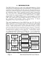
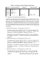
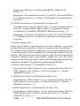
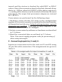
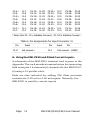
MSI-P420 MSI-P421 MSI-P422 ANALOG INPUT CARD USER MANUAL PC/104 Embedded Industrial Analog I/O Series Microcomputer Systems, Inc. 1814 Ryder Drive ¨ Baton Rouge, LA 70808 Ph (504)769-2154 ¨ Fax (504) 769-2155 Email: [email protected] http://www.microcomputersystems.com Page MSI-P420/P421/P422 User Manual CONTENTS I. INTRODUCTION 3 II.HARDWARE DESCRIPTION 5 5 6 A. Card Configuration B. Card Addressing C. Conversion Registers D. Interrupt Hardware Connections 6 10 E. Performing a Conversion F. Connecting Inputs to P1 and P2 10 11 G. Using the MSI-P910 and 20 mA Current Inputs 12 III. 'C' PROGRAM EXAMPLE 14 III. SPECIFICATIONS 16 APPENDIX 17 Circuit Diagrams MSI-P420/P421/P422 MSI-P910 MAX13xx.pdf Page MSI-P420/P421/P422 User Manual I. INTRODUCTION The MSI-P42x series is a low cost, high performance 12-bit analog input card designed for use with all PC/104 embedded systems. A special feature for the series is the simultaneous conversion of all channels activated from software or from an external pulse. Four models provide input capacities of 8, 16, 24 or 32 channels which operate from a single +5V supply for input ranges of 0-5V (MSI-P420), ±5V (MSIP421) and ±10V (MSI-P422) with a non-linearity of ±1/2 LSB. The inputs are overvoltage tolerant to +9V and ±15V for unipolar and bipolar units, respectively. A block diagram of the card is shown in Fig. 1. PC/104 16-BIT STACKTHROUGH CONNECTOR The card employs up to four MAX13xx, xx= 04, 08 or 12) eight-channel A/D converters that incorporate a precision 2.5V reference source with buffer amp, an internal 15 MHz clock, and independent track-and-hold (T/H) circuitry provides simultaneous sampling of each channel. Channels for each of four devices can be enabled or disabled via the configuration register of the devices. Conversion times are approximately 800ns to 2200ns for 1 to 8 channels, respectively, for each device. Since conversions are A8-A15 JUMPERS PC/104 BUS INTERFACE NETWORK IRQ2-IRQ15 JUMPERS MAX13XX SERIES 8-CH CONVERTER (CH 0 to 7) MAX13XX SERIES 8-CH CONVERTER (CH 8 to 15) MAX13XX SERIES 8-CH CONVERTER (CH 16 to 23) MAX13XX SERIES 8-CH CONVERTER (CH 24 to 31) 34-PIN CONNECTOR ANALOG INPUTS (CH 0 to 15) 2-PIN CONNECTOR START CONVERT IN 34-PIN CONNECTOR ANALOG INPUTS (CH 16 to 31) MSI-P420/P421/P422 Figure 1. Block Diagram of the MSI-P420/P421/P422. Page 3 MSI-P420/P421/P422 User Manual MSI-P416 ISOLATED simultaneous, all four devices are converting at the same time for a maximum time of approximately 2200ns for all 32 channels. A detailed description of the conversion devices is the MAX13xx.pdf document in the Appendix. The card is I/O mapped using 16-bit addressing to select the input channels and device status. Option jumpers are provided for specifying the card base addresses A8 thru A15 and interrupts IRQ2 thru IRQ15, as described in the next section. The MSI-P910 terminal card can be used to provide up to 16 analog inputs via terminal strips. This card contains resistor sites for accommodating current inputs of 0-20 mA or 4-20 mA and includes surge protection for protecting against spurious voltages prevalent in harse or industrial environments. Page 4 MSI-P420/P421/P422 User Manual II. HARDWARE DESCRIPTION A. Card Configuration The MSI-C420/P421/P422 card is a CMOS design using through-hole and surface-mounted devices. The card configuration is shown in Figure 2 and a circuit diagram of the network is given in the Appendix. The input signals for channels 0 thru 15 are applied to connector J1 and channels 16 thru 31 to J2. These signals are directed to the input terminals of A/D converters U11 (Ch. 0-7), U14 (Ch. 8-15), U17 (Ch. 16-23) and U20 (Ch. 24-31). Jumper block JP1 is used for base address selection (Pins 1 thru 16) and interrupt configuration (Pins 19 thru 38), as described below. A 1 KOhm pull-down resistor for use with Figure 2. MSI-P420/P421/P422 card outline. Page 5 MSI-P420/P421/P422 User Manual the interrupts is available on pins 17-18. B. Card Addressing The card base address is set by installing appropriate jumpers on JP1, pins 1 thru 16, as shown in Fig. 3. An uninstalled jumper for a given address bit sets the bit to 0 (false) and an installed jumper sets the bit to 1 (true). Addresses A8 thru A15 are jumper selectable for defining the base address of the card from 0000H to FF00H on integral 100H boundaries, where H denotes a hexadecimal number. To assign a base address of 8200H, for example, install jumpers JP1-13,14 (A9) and JP1-1,2 (A15). Pins 17 thru 38 are used to configure the interrupt connections, if interrupts are used, as described in the Section II.D. C. Conversion Registers The MAX13xx converters each have five types of registers for performing data conversions, a Configuration register (C), an input Data register (D), a convert Status register (S), a convert status Reset register (R), and an Initiate convert register (I). The addresses for each device are summarized in Table 1. 1. Configuration register (C) 32 IRQ15 34 IRQ14 36 IRQ12 38 IRQ11 o o o o o o o o o o o o o o o o o o o o o o o o o 3 5 17 19 21 31 33 35 37 29 27 25 23 13 11 9 30 IRQ10 22 IRQ7 o 28 IRQ3 20 IRQ2(9) o 26 IRQ4 18 1 KOhm o 24 IRQ5 16 A8 o 15 o 14 A9 A12 8 o 12 A10 A13 6 o 10 A11 A14 4 o 7 A15 2 o 1 Four configuration registers are used to enable or Figure 3. Jumper block JP1 configuration. Page 6 MSI-P420/P421/P422 User Manual Table 1. Analog Converter Register Addresses Channels Control & Data(C/D) 0-7 base + 0 8-15 base + 2 16-23 base + 4 24-31 base + 6 0-31 Status(S) base + 8 Start Convert(I) base + CH* * - Denotes a hexadecimal address. disable the analog channels of each device. Bits 0 thru 7 are used to set the mode of a channel and bits 8 thru 15 are ignored. A 0 bit setting disables the channel and a 1 enables the channel. Disabled channels are not converted and the overall conversion time is reduced by approximately 200ns for each disabled channel of the device. Devices are configured as follow. a. MAX13xx Device 1 (Channels 0 thru 7) Configuration format: Bits 0 thru 7 control channels 0 thru 7, respectively. Bits 8 thru 15 ignored. Power-up default is enabled (FFFFH). Address is base + 0. Example: To enable channels 0 and 5, write FF20H to I/O address base + 0, where H denotes a hexadecimal number. b. MAX13xx Device 2 (Channels 8 thru 15) Configuration format: Bits 0 thru 7 control channels 8 thru 15, respectively. Bits 8 thru 15 ignored. Power-up default is enabled (FFFFH). Address is base + 2. Example: To enable channels 9 and 14, write FF42H to I/O address base + 2, where H denotes a hexadecimal number. c. MAX13xx Device 3 (Channels 16 thru 23) Configuration format: Bits 0 thru 7 control channels 16 thru 23, respectively. Bits 8 thru 15 ignored. The Page 7 MSI-P420/P421/P422 User Manual power-up default is enabled (FFFFH). Address is base + 4. Example: To enable channels 17 and 23, write FF82H to I/O address base + 4, where H denotes a hexadecimal number. d. MAX13xx Device 4 (Channels 24 thru 31) Configuration format: Bits 0 thru 7 control channels 24 thru 31, respectively. Bits 8 thru 15 ignored. Powerup default is enabled (FFFFH). Address is base + 6. Example: To enable channels 27 and 30, write FF48H to I/O address base + 6, where H denotes a hexadecimal number. 2. Data register (D) Four input data registers provide for reading converted values from the devices. Data is retrieved by successive I/O reads of each device. Each device is read repeatedly for a count equal to the number of channels enabled in the device. The first value read is equal to the lowest numbered enabled channel and successive reads are for the next lowest until the last read, which is the highest numbered enabled channel. Reads are performed as follow. a. MAX13xx Device 1 (Channels 0 thru 7) Data format: Bits 0 thru 11 are converted data, Bit 0 is LSB. Ignore bits 12 thru 15 that are set to 1. Read address is base + 0. b. MAX13xx Device 2 (Channels 8 thru 15) Data format: Bits 0 thru 11 are converted data, Bit 0 is LSB. Ignore bits 12 thru 15 that are set to 1. Read address is base + 2. c. MAX13xx Device 3 (Channels 16 thru 23) Data format: Bits 0 thru 11 are converted data, Bit 0 is LSB. Ignore bits 12 thru 15 that are set to 1. Read address is base + 4. Page 8 MSI-P420/P421/P422 User Manual d. MAX13xx Device 4 (Channels 24 thru 31) Data format: Bits 0 thru 11 are converted data, Bit 0 is LSB. Ignore bits 12 thru 15 that are set to 1. Read address is base + 6. 3. Status register (S) The conversion status register provides the EOC and EOLC bit values by performing an I/O read at address base + 8. Bit 0 of the status is EOC and bit 1 is EOLC. Bits 2 thru 15 are set to 1. The EOC bit is latched by the NANDing of the EOC's from each converter. This bit is 1 when the first channel of any device is converted and is ready for reading and 0 otherwise. The EOLC bit is latched by the NANDing of the EOLC's from each converter. This bit is 1 when the last channel of any device is converted and is ready for reading and 0 otherwise. 4. Initiate convert register (I) The initiate convert register is used to start a conversion sequence for all devices. Conversions can be performed in two ways as follow. a. Software Initiated - An I/O write of any value to address base + CH will initiate simultaneous conversions on all devices which will require a maximum time of approximately 2200ns if all 8 channels are enabled any one of the devices. b. Hardware Initiated - An input pulse applied to J1-17 and J1-18 (see Table 2) or J3-1 and J3-2 (see Table 3) will initiate a conversion sequence. A 4.7KOhm pull-up is used on these inputs to provide compatibility with opencollector and relay contact inputs. TTL inputs are valid as well. The conversion is initiated on the rising edge of the input pulse. As in the software initiated case, simultaneous conversions on all devices which will require a maximum time of approximately 2200ns if all 8 Page 9 MSI-P420/P421/P422 User Manual channels are enabled any one of the MAX13xx devices. D. Interrupt Hardware Connections Interrupt connections are implemented by pins 17 thru 38 of JP1 and interrupt source selection jumpers of JP3. Interrupts are most commonly used with external hardware initated conversions. Note: User must supply program code for processing of interrupts. The steps in the procedure are as follows. 1. Select the interrupting source using JP3 jumper. a. End-of-last-conversion (EOLC) JP3-1,2. The EOLC signal, described above, is valid when the last channel of any device is converted and is ready for reading. b. End-of-conversion (EOC) JP3-2,3. The EOC signal, described above, is valid when the first channel of any device is converted and is ready for reading. 2. Select the desired IRQ using a jumper on pins 19 thru 38 of JP1 as follows. IRQ2: JP1-19,20 IRQ3: JP1-27,28 IRQ4: JP1-25,26 IRQ5: JP1-23,24 IRQ7: JP1-21,22 IRQ10: JP1-29,30 IRQ11: JP1-37,38 IRQ12: JP1-35,36 IRQ14: JP1-33,34 IRQ15: JP1-31,32 A 1 KOhm pull-down resistor is available on JP1-17,18. Only 1 resistor should be enabled in the system for a given IRQ when multiple peripheral cards are used. E. Performing a Conversion Conversions can be made in a polling mode or an interrupt driven mode. Polling is normally used when the conversion is activated under software control. An intiate convert is Page 10 MSI-P420/P421/P422 User Manual issued and the status is checked for valid EOC or EOLC values. Since the conversion time for the first channel of any device is ~900ns, when bit 0 (EOC) of the status register is 1, reading of the devices can be started at this time for most processors. For super fast processors simply use instead bit 1 (EOLC). Conversions are performed by the following steps. 1.Perform a word (16-bit) I/O write to the configuration register (C) for each converter to enable the desired number of channels of each device. Default setting at power-up is all channels are enabled. This step is only required if the channels enabled are to be changed. 2.Initate a conversion by software or hardware as described in C.4 above. 3.Read the converted data as outlined in C.2 above. Note: User must supply program code for processing of data using interrupts. F. Connecting Inputs to J1 and J2. Inputs are interconnected to the card via P1 and P2 using 34-pin flat cable connectors. Pin assignments are given in Table 2. Table 2. Pin assignments for Input Connectors J1 and J2. Chan Pin Input Pin Chan Pin Input Pin Ch 0+ Ch 0- J1-17* J1-18* J1-15 J1-16 Init convert+ Init convert - (GND) Ch 8+ J1-33 Ch 16+ Ch 8J1-34 Ch 16- Ch 1+ Ch 1- J1-13 J1-14 Ch 9+ Ch 9- Ch 2+ Ch 2Ch 3+ Ch 3- Page J2-17 J2-18 J2-15 J2-16 +5V GND Ch 24+ J2-33 Ch 24- J2-34 J1-31 J1-32 Ch 17+ J2-13 Ch 17- J2-14 Ch 25+ J2-31 Ch 25- J2-32 J1-11 J1-12 Ch 10+ J1-29 Ch 10- J1-30 Ch 18+ J2-11 Ch 18- J2-12 Ch 26+ J2-29 Ch 26- J2-30 J1-9 J1-10 Ch 11+ J1-27 Ch 11- J1-28 Ch 19+ J2-9 Ch 19- J2-10 Ch 27+ J2-27 Ch 27- J2-28 11 MSI-P420/P421/P422 User Manual Ch 4+ Ch 4- J1-7 J1-8 Ch 12+ J1-25 Ch 12- J1-26 Ch 20+ J2-7 Ch 20- J2-8 Ch 28+ J2-25 Ch 28- J2-26 Ch 5+ Ch 5- J1-5 J1-6 Ch 13+ J1-23 Ch 13- J1-24 Ch 21+ J2-5 Ch 21- J2-6 Ch 29+ J2-23 Ch 29- J2-24 Ch 6+ Ch 6- J1-3 J1-4 Ch 14+ J1-21 Ch 14- J1-22 Ch 22+ J2-3 Ch 22- J2-4 Ch 30+ J2-21 Ch 30- J2-22 Ch 7+ Ch 7- J1-1 J1-2 Ch 15+ J1-19 Ch 15- J1-20 Ch 23+ J2-1 Ch 23- J2-2 Ch 31+ J2-19 Ch 31- J2-20 * Note: Pins P1-17 is Initialize Convert+, P1-18 is Initialize Convert -. Table 3. Pin assignments for Input Connector J3. Pin Input Pin Input Pin J3-1* Init convert+ J3-2 Init convert - (GND) G. Using the MSI-P910 and 20mA Current Inputs. A schematic of the MSI-P910 terminal card is given in the Appendix. The card provides terminal strips for connecting field wiring for 16 channels (8 channels for the MSI-P9108) using a 34-pin flat cable. Pads are also included for adding 250 Ohm precision resistors for 0-20 mA or 4-20 mA inputs. Normally, the MSI-P420 is used for current inputs. Page 12 MSI-P420/P421/P422 User Manual BLANK PAGE Page 13 MSI-P420/P421/P422 User Manual III. 'C' PROGRAM EXAMPLE A simple 'C' program for performing a software mode conversion sequence is given below. The program initializes the card and initiates a polled mode acquisition sequence. The data is displayed on the user console device. /* Program to test P420 Card - 09/16/2009 */ clear_screen() { char a; for (a=1; a<=25; a=a+1) printf(“\n”); } main() { char buffer[10]; int sel0, sel1, sel2, sel3, sel4, sel6, baddr, sel; baddr = 0x300; sel0 = baddr; /* control, data ch 0-7 */ sel1 = baddr + 0x2; /* control, data ch 8-15 */ sel2 = baddr + 0x4; /* control, data ch 16-23 */ sel3 = baddr + 0x6; /* control, data ch 24-31 */ sel4 = baddr + 0x8; /* status, EOC = bit0, EOLC = bit2 */ sel6 = baddr + 0xc; /* start convert */ start: clear_screen; /* printf(“(1) Input channels 0-7\n”); printf(“\n”); printf(“Input choice - “); gets(buffer); printf(buffer[0]); gets(buffer); if( buffer == 1 ) { printf(“it is 1”); } gets(buffer);*/ { outportw(sel0, 0xff); /* init all ports for 8 channels */ outportw(sel1, 0xff); Page 14 MSI-P420/P421/P422 User Manual outportw(sel2, 0xff); outportw(sel3, 0xff); printf(“Status (should be 0xfc) = “); printf(“%X\n”,inportw(sel4)); gets(buffer); outportw(sel6, 0); /* start conversion */ printf(“Status (should be 0xff) = “); printf(“%X\n”,inportw(sel4)); gets(buffer); sel = sel0; printf(“Ch 7-0 = “); printf(“%X %X %X %X %X %X %X %X\n”, inportw(sel), inportw(sel), inportw(sel), inportw(sel), inportw(sel), inportw(sel), inportw(sel), inportw(sel)); printf(“Strike any key to continue”); gets(buffer); sel = sel1; printf(“Ch 15-8 = “); printf(“%X %X %X %X %X %X %X %X\n”, inportw(sel), inportw(sel), inportw(sel), inportw(sel), inportw(sel), inportw(sel), inportw(sel), inportw(sel)); printf(“Strike any key to continue”); gets(buffer); sel = sel2; printf(“Ch 23-16 = “); printf(“%X %X %X %X %X %X %X %X\n”, inportw(sel), inportw(sel), inportw(sel), inportw(sel), inportw(sel), inportw(sel), inportw(sel), inportw(sel)); printf(“Strike any key to continue”); gets(buffer); sel = sel3; printf(“Ch 31-24 = “); printf(“%X %X %X %X %X %X %X %X\n”, inportw(sel), inportw(sel), inportw(sel), inportw(sel), inportw(sel), inportw(sel), inportw(sel), inportw(sel)); printf(“Strike any key to continue”); gets(buffer); } goto start; } Page 15 MSI-P420/P421/P422 User Manual IV. SPECIFICATIONS PC/104 Analog Inputs Channels Converter MSI-P420 MSI-P421 MSI-P422 Single-endedInput Ranges MSI-P420 MSI-P421 MSI-P422 Resolution Conversion Rate Non-linearity OffsetError GainError Signal-to-Noise InputResistance Internal Reference Ref Out Voltage Temp. Coeff. Connectors MSI-P42x-8Ch MSI-P42x-16Ch MSI-P42x-24Ch 16-bit,stackthrough 8 to 32 in groups of 8 MAX1304 MAX1308 MAX1312 0-5V ±5V ±10V 12bits 456 ksps per channel, 32 Ch's enabled ±1/2LSBtypical ±3LSBtypical ±2LSBtypical 71dBtypical 1 MΩ standard (10 MΩ optional) 2.5 V ±1% 30 ppm/°C One (1) 3M 30320-5002 or eq. (20-pin) One (1) 3M 30334-5002 or eq. (34-pin) One (1) 3M 30316-5002 or eq. (16-pin) One (1) 3M 30334-5002 or eq. (34-pin) Two (2) 3M 30334-5002 or eq. (34-pin) MSI-P42x-32Ch Interrupts Channels One,sharingwithtri-statebufferforIRQ2-15 Option Jumpers .025"squareposts,0.1"grid Electrical & Environmental +5V @ 300 mA typical, 32 Ch's enabled -40° to 85°C Page 16 MSI-P420/P421/P422 User Manual APPENDIX Circuit Diagrams MSI-P420/P421/P422 see P420-1.pdf, P420-2.pdf, P420-2.pdf, P420-3.pdf, P420-4.pdf and P420-5.pdf MSI-P910 see P910.pdf MAX13xx Document see MAX13xx.pdf Page 17 MSI-P420/P421/P422 User Manual