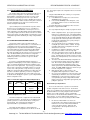
1
Series IP1K110 Industrial I/O Pack Reconfigurable Digital I/O Board USER’S MANUAL ACROMAG INCORPORATED 30765 South Wixom Road P.O. BOX 437 Wixom, MI 48393-7037 U.S.A. [email protected] Copyright 2004-2011, Acromag, Inc., Printed in the USA. Data and specifications are subject to change without notice. Tel: (248) 295-0310 Fax: (248) 624-9234 8500-724-F11M004 SERIES IP1K110 INDUSTRIAL I/O PACK RECONFIGURABLE DIGITAL I/O MODULE _________________________________________________________________________________________ The information contained in this manual is subject to change without notice. Acromag, Inc. makes no warranty of any kind with regard to this material, including, but not limited to, the implied warranties of merchantability and fitness for a particular purpose. Further, Acromag, Inc. assumes no responsibility for any errors that may appear in this manual and makes no commitment to update, or keep current, the information contained in this manual. No part of this manual may be copied or reproduced in any form, without the prior written consent of Acromag, Inc. Table of Contents Page 1.0 GENERAL INFORMATION…....................................... 2 KEY IP1K110 FEATURES............................................ 3 INDUSTRIAL I/O PACK INTERFACE FEATURES........ 3 SIGNAL INTERFACE PRODUCTS............................... 3 IP MODULE Win32 DRIVER SOFTWARE…………….. 4 IP MODULE VxWORKS SOFTWARE........................... 4 2.0 PREPARATION FOR USE............................................ 4 UNPACKING AND INSPECTION.................................. 4 CARD CAGE CONSIDERATIONS................................ 4 BOARD CONFIGURATION........................................... 4 CONNECTORS............................................................. 4 IP Field I/O Connector (P2)....................................... 4 I/O Noise and Grounding Considerations.................. 5 IP Logic Interface Connector (P1).............................. 5 3.0 PROGRAMMING INFORMATION................................. 6 IN-SYSTEM CONFIGURATION ADDRESS MAPS....... 6 IP1K110 Configuration Procedure............................. 6 Altera FPGA Logic Requirements.............................. 6 IP Identification Space............................................... 7 Example Altera FPGA Design................................... 7 Control Register........................................................ 8 Input/Output Registers............................................... 9 Direction Control Register.......................................... 9 Interrupt Enable Register........................................... 9 Interrupt Type Configuration Register........................ 9 Interrupt Status Register............................................ 10 Interrupt Polarity Register.......................................... 10 Interrupt Vector Register........................................... 10 Memory Data Register............................................... 10 Memory Address Register......................................... 11 Clock Control Register 1 ........................................... 11 Clock Control Register 2 ........................................... 11 Clock Control Register 3 ........................................... 11 Clock Trigger Register............................................... 11 Program Procedure to Set Clock Frequency............. 11 IP1K110 PROGRAMMING CONSIDERATIONS........... 12 Programming Interrupts............................................. 12 4.0 THEORY OF OPERATION........................................... 13 FIELD INPUT/OUTPUT SIGNALS................................. 13 LOGIC/POWER INTERFACE....................................... 13 EIA-RS485 AND RS422 SERIAL INTERFACE.............. 14 SIGNAL PIN ASSIGNMENTS....................................... 14 5.0 SERVICE AND REPAIR................................................ 16 SERVICE AND REPAIR ASSISTANCE........................ 16 PRELIMINARY SERVICE PROCEDURE...................... 16 6.0 SPECIFICATIONS........................................................ 16 PHYSICAL.................................................................... 16 ENVIRONMENTAL........................................................ 17 EIA-RS485/RS422 TRANSCEIVERS............................ 17 TTL TRANSCEIVERS................................................... 17 INDUSTRIAL I/O PACK COMPLIANCE........................ 17 IP1K110 ENGINEERING DESIGN KIT.......................... 18 APPENDIX................................................................... CABLE: MODEL 5025-551............................................ CABLE: MODEL 5025-552............................................ TRANSITION MODULE: MODEL TRANS-GP............... 18 18 18 19 DRAWINGS 4501-971 IP1K110 BLOCK DIAGRAM......................... 4501-702 RS485 I/O CONNECTIONS.......................... 4501-434 IP MECHANICAL ASSEMBLY..................… 4501-462 CABLE 5025-550 (NON-SHIELDED)............ 4501-463 CABLE 5025-551 (SHIELDED)..................... 4501-464 TERMINATION PANEL 5025-552................ 4501-465 TRANSITION MODULE TRANS-GP............ Page 20 21 22 23 24 25 25 IMPORTANT SAFETY CONSIDERATIONS It is very important for the user to consider the possible adverse effects of power, wiring, component, sensor, or software failures in designing any type of control or monitoring system. This is especially important where economic property loss or human life is involved. It is important that the user employ satisfactory overall system design. It is agreed between the Buyer and Acromag, that this is the Buyer's responsibility. All trademarks are the property of their respective owners. 1.0 GENERAL INFORMATION The Industrial I/O Pack (IP) Series IP1K110 module is a reconfigurable digital input/output board. The IP1K110 contains a 100,000 gate Altera Field Programmable Gate Array (FPGA) which is in-system reconfigurable. This allows designers to implement logic functions unique to their application and insystem configure the Altera FPGA via the IP bus interface. An example Altera FPGA configuration file and its corresponding VHDL source are provided with the IP1K110 Engineering Design Kit. To take advantage of the example VHDL program, the user must be proficient in the use of VHDL and the Altera Maxplus II or Quartus II software tools. The IP1K110 provides several different interface options which allow a mix of differential digital and TTL digital input/output channels. The models and their corresponding combination of channels are given in the table below. Model IP1K110-0024 IP1K110-2412 IP1K110-4800 IP1K110-0024E IP1K110-2412E IP1K110-4800E TTL Channels EIA-485/422 Channels 0 24 48 0 24 48 24 12 0 24 12 0 Operating Temperature Range 0 to 70°C 0 to 70°C 0 to 70°C -40 to 85°C -40 to 85°C -40 to 85°C The IP1K110 can be programmed to support all types of IP cycles at either 8 or 32 MHz operation. The IP1K110 comes with a simple example Altera design file that can be enhanced for implementation of custom digital logic functions. -2Acromag, Inc. Tel:248-295-0310 Fax:248-624-9234 Email:[email protected] http://www.acromag.com SERIES IP1K110 INDUSTRIAL I/O PACK RECONFIGURABLE DIGITAL I/O MODULE __________________________________________________________________________________________ The example design supplied with the IP1K110 is provided as a VHDL file for Altera’s Max+Plus II or Quartus II software. The example design includes an IP bus interface to ID space, IO space and Interrupt space. IO space is used to access a 64K x 16 RAM array, control field data I/O, and control a clock generation chip. The IP1K110 utilizes state of the art Surface-Mounted Technology (SMT) to achieve its high channel density and is an ideal choice for a wide range of industrial control and monitor applications that require high-density, high-reliability, and highperformance at a low cost. KEY IP1K110 FEATURES • Reconfigurable Altera FPGA – In system configuration of a 100,000 gate FPGA is implemented via the IP bus interface. This provides a means for implementation of custom user defined digital designs. • IP Bus Interface – The Altera FPGA is directly connected to all IP bus logic signals. Custom designs can thus support all IP module access types including ID, I/O, Interrupt, Memory, and DMA. • High Channel Count Digital Interface – Differential and TTL interface options are allowed. Interfaces with up to 24 differential, or a mix of 12 differential and 24 TTL, or up to 48 TTL digital input/output channels. • Channel Input/Output Control – The bidirectionality of the TTL digital channels is controlled in groups of 8 channels. The bidirectionality of the differential digital signals is controlled in groups of 4 channels. • Long Distance Data Transmission – Data transmission with RS485/RS422 Transceivers allow up to 32 nodes and up to 4000 feet of transmission cable. • 64K x 16 SRAM – A 64K x 16 static random access memory (SRAM) is directly accessed by the Altera device. Custom user defined design logic for the Altera FPGA will permit use of the SRAM as FIFO memory, or single port memory as required by the application. • Example Design Provided – Example VHDL design which includes implementation of the IP bus interface and control of digital I/O with software programmable Interrupts is provided. • Clock Speed – Supports an 8 or 32 MHz IP bus clock speed. • Programmable Clock Generator – A clock generator IC is provided for applications requiring a custom user specified clock frequency. The clock generator can be programmed to any desired frequency value between 250KHz and 100MHz. • No Configuration Jumpers or Switches – All configuration is performed through software commands with no internal jumpers to configure or switches to set. • Power Up & System Reset is Failsafe – For safety, all channels are configured as input upon power-up and after a system reset. INDUSTRIAL I/O PACK INTERFACE FEATURES • High density - Single-size, industry-standard, IP module footprint. Up to four units may be mounted on a 6U VMEbus carrier board or five units may be mounted on a PCI carrier board. • Local ID - Each IP module has its own 8-bit ID information which is accessed via data transfers in the "ID Read" space. • 16-bit & 8-bit I/O - Channel register Read/Write is performed through D16 or D08 (EO) data transfer cycles in the IP module I/O space. • High Speed - Access times for all data transfer cycles are described in terms of "wait" states. For the supplied IP module example, wait states are utilized for all read and write operations (see specifications for detailed information). SIGNAL INTERFACE PRODUCTS (See Appendix for more information on compatible products) This IP module will mate directly to any industry standard IP carrier board. A wide range of other Acromag IP modules and carriers are also available to serve your signal conditioning and interface needs. The cables and termination panels, described in the following paragraphs, represent some of the accessories available from Acromag. Each Acromag carrier has its own unique accessories. They are not all listed in this document. Consult your carrier board documentation for the correct interface product part numbers to ensure compatibility with your carrier board. Cables: Model 5025-551-X (Shielded Cable), or Model 5025-550-X (Non-Shielded Cable): A Flat 50-pin cable with female connectors at both ends for connecting AVME9630/9660, or other compatible carrier boards, to Model 5025-552 termination panels. The unshielded cable is recommended for digital I/O, while the shielded cable is recommended for optimum performance with precision analog I/O applications. Termination Panel: Model 5025-552: A DIN-rail mountable panel that provides 50 screw terminals for universal field I/O termination. Connects to all Acromag carriers (or other compatible carrier boards) via flat 50-pin ribbon cable (Model 5025-550-X or 5025-551-X). Transition Module: Model TRANS-GP: This module repeats field I/O connections of IP modules A through D for rear exit from a VMEbus card cage. It is available for use in card cages which provide rear exit for I/O connections via transition modules (transition modules can only be used in card cages specifically designed for them). It is a double-height (6U), single-slot module with front panel hardware adhering to the VMEbus mechanical dimensions, except for shorter printed circuit board depth. It connects to Acromag Termination Panel 5025-552 from the rear of the card cage, and to AVME9630/9660 boards within the card cage, via flat 50-pin ribbon cable (Model 5025-550-X or 5025-551-X). IP1K110 FPGA ENGINEERING DESIGN KIT Acromag provides an engineering design kit for the IP1K110 (sold separately), a “must buy” for first time IP1K110 module purchasers. The design kit (model IP-1K110-EDK) provides the user with the basic information required to develop a custom FPGA program for download to the Altera FPGA. The design kit includes a CD containing: schematics, parts list, part location drawing, example VHDL source, example configuration file, and other utility files. The IP1K110 is intended for users fluent in the use of Altera MaxPlus II or Quartus II design tools. -3Acromag, Inc. Tel:248-295-0310 Fax:248-624-9234 Email:[email protected] http://www.acromag.com SERIES IP1K110 INDUSTRIAL I/O PACK RECONFIGURABLE DIGITAL I/O MODULE __________________________________________________________________________________________ IP MODULE Win32 DRIVER SOFTWARE CARD CAGE CONSIDERATIONS Acromag provides a software product (sold separately) to facilitate the development of Windows (2000/XP/Vista/7) applications accessing Industry Pack modules installed on Acromag PCI Carrier Cards and CompactPCI Carrier Cards. This software (Model IPSW-API-WIN) consists of low-level drivers and Windows 32 Dynamic Link Libraries (DLLS) that are compatible with a number of programming environments including Visual C++, Visual Basic, Borland C++ Builder and others. The DLL functions provide a high-level interface to the carriers and IP modules eliminating the need to perform low-level reads/writes of registers, and the writing of interrupt handlers. Refer to the specifications for loading and power requirements. Be sure that the system power supplies are able to accommodate the power requirements of the carrier board, plus the installed IP modules, within the voltage tolerances specified. IP MODULE VxWORKS SOFTWARE Acromag provides a software product (sold separately) consisting of IP module VxWorks libraries. This software (Model IPSW-API-VXW MSDOS format) is composed of VxWorks (real time operating system) libraries for all Acromag IP modules and carriers. The software is implemented as a library of “C” functions which link with existing user code to make possible simple control of all Acromag IP modules and carriers. The IP1K110 support programs implement the transfer of developed code between the user’s processor and the Altera FPGA. IMPORTANT: Adequate air circulation must be provided to prevent a temperature rise above the maximum operating temperature. The dense packing of the IP modules to the carrier board restricts air flow within the card cage and is cause for concern. Adequate air circulation must be provided to prevent a temperature rise above the maximum operating temperature and to prolong the life of the electronics. If the installation is in an industrial environment and the board is exposed to environmental air, careful consideration should be given to air-filtering. BOARD CONFIGURATION 2.0 PREPARATION FOR USE Power should be removed from the board when installing IP modules, cables, termination panels, and field wiring. Refer to Mechanical Assembly Drawing 4501-434 and the following discussion for configuration and assembly instructions. Model IP1K110 I/O Boards have no jumpers or switches to configure— all configuration is through software commands. UNPACKING AND INSPECTION CONNECTORS Upon receipt of this product, inspect the shipping carton for evidence of mishandling during transit. If the shipping carton is badly damaged or water stained, request that the carrier's agent be present when the carton is opened. If the carrier's agent is absent when the carton is opened and the contents of the carton are damaged, keep the carton and packing material for the agent's inspection. IP Field I/O Connector (P2) For repairs to a product damaged in shipment, refer to the Acromag Service Policy to obtain return instructions. It is suggested that salvageable shipping cartons and packing material be saved for future use in the event the product must be shipped. This board is physically protected with packing material and electrically protected with an anti static bag during shipment. However, it is recommended that the board be visually inspected for evidence of mishandling prior to applying power. The board utilizes static sensitive components and should only be handled at a static-safe workstation. P2 provides the field I/O interface connector for mating IP modules to the carrier board. P2 is a 50-pin female receptacle header (AMP 173279-3 or equivalent) which mates to the male connector of the carrier board (AMP 173280-3 or equivalent). This provides excellent connection integrity and utilizes goldplating in the mating area. Threaded metric M2 screws and spacers are supplied with the module to provide additional stability for harsh environments (see Mechanical Assembly Drawing 4501-434). The field and logic side connectors are keyed to avoid incorrect assembly. P2 pin assignments are unique to each IP model (see Table 2.1) and normally correspond to the pin numbers of the field-I/O interface connector on the carrier board (you should verify this for your carrier board). When reading Table 2.1 notice that RS485 input/output channels as well as digital TTL input/output channels are listed with their corresponding connector pin number. Each I/O point will be either RS485 or TTL defined by your IP1K110 model. Table 2.2 lists the channels dedicated to each of the IP1K110 models. -4Acromag, Inc. Tel:248-295-0310 Fax:248-624-9234 Email:[email protected] http://www.acromag.com SERIES IP1K110 INDUSTRIAL I/O PACK RECONFIGURABLE DIGITAL I/O MODULE __________________________________________________________________________________________ Table 2.1: IP1K110 Field I/O Pin Connections (P2) Pin Description RS485 TTL I/O00+ I/O00 I/O00I/O01 I/O01+ I/O02 I/O01I/O03 I/O02+ I/O04 I/O02I/O05 I/O03+ I/O06 I/O03I/O07 I/O04+ I/O08 I/O09 I/O04I/O05+ I/O10 I/O05I/O11 I/O06+ I/O12 I/O06I/O13 I/O14 I/O07+ I/O07I/O15 I/O08+ I/O16 I/O08I/O17 I/O09+ I/O18 I/O09I/O19 I/O10+ I/O20 I/O10I/O21 I/O11+ I/O22 I/O11I/O23 I/O12+ I/O24 Pin Number 1 2 3 4 5 6 7 8 9 10 11 12 13 14 15 16 17 18 19 20 21 22 23 24 25 Pin Description RS485 TTL I/O12I/O25 I/O13+ I/O26 I/O13I/O27 I/O14+ I/O28 I/O14I/O29 I/O15+ I/O30 I/O15I/O31 I/O16+ I/O32 I/O16I/O33 I/O17+ I/O34 I/O17I/O35 I/O18+ I/O36 I/O18I/O37 I/O19+ I/O38 I/O39 I/O19I/O20+ I/O40 I/O20I/O41 I/O21+ I/O42 I/O21I/O43 I/O22+ I/O44 I/O22I/O45 I/O23+ I/O46 I/O23I/O47 NC NC GND GND Pin Number 26 27 28 29 30 31 32 33 34 35 36 37 38 39 40 41 42 43 44 45 46 47 48 49 50 Table 2.2: IP1K110 Model Channel Assignments Model I/O Register Bits See Table 2.1 for Pin Assignments IP1K110-0024 Differential/RS485 Channels ±0 to ±23 IP1K110-2412 IP1K110-4800 Differential /RS485 Channels ±12 to ±23 TTL Channels 0 to 23 TTL Channels 0 to 47 I/O Noise and Grounding Considerations The IP1K110 is non-isolated between the logic and field I/O grounds since output common is electrically connected to the IP module ground. Consequently, the field I/O connections are not isolated from the carrier board and backplane. Two ounce copper ground plane foil has been employed in the design of this model to help minimize the effects of ground bounce, impedance drops, and switching transients. However, care should be taken in designing installations without isolation to avoid noise pickup and ground loops caused by multiple ground connections. To minimize high levels of EMI the signal ground connection at the field I/O port (pin 50) should be used to provide a path for induced common-mode noise and currents. The ground path provides a low-impedance path to reduce emissions. be at the ends of long branches, spokes, or stubs. See Drawing 4501-702 for example connection and termination practices. Transmission line signal reflections can be minimized with proper termination. The EIA RS485/RS422 standard allows up to 32 driver/receivers to be connected to a single bus. Termination resistors should only be used at the two extreme ends of the bus and not at each of the nodes of the bus. Termination resistors are not provided on the IP1K110. They can be added to the field wiring as near to the IP module as possible. IP Logic Interface Connector (P1) P1 of the IP module provides the logic interface to the mating connector on the carrier board. This connector is a 50-pin female receptacle header (AMP 173279-3 or equivalent) which mates to the male connector of the carrier board (AMP 173280-3 or equivalent). This provides excellent connection integrity and utilizes gold-plating in the mating area. Threaded metric M2 screws and spacers are supplied with the IP module to provide additional stability for harsh environments (see Drawing 4501-434 for assembly details). Field and logic side connectors are keyed to avoid incorrect assembly. The pin assignments of P1 are standard for all IP modules according to the Industrial I/O Pack Specification (see Table 2.3). Note that the IP1K110 does not utilize all of the logic signals defined for the P1 connector and these are indicated in BOLD ITALICS. Table 2.3: Standard Logic Interface Connections (P1) Pin Description GND CLK Reset∗ D00 D01 D02 D03 D04 D05 D06 D07 D08 D09 D10 D11 D12 D13 D14 D15 BS0∗ BS1∗ -12V +12V +5V GND Number 1 2 3 4 5 6 7 8 9 10 11 12 13 14 15 16 17 18 19 20 21 22 23 24 25 Pin Description GND +5V R/W ∗ IDSEL∗ DMAReq0∗ MEMSEL∗ DMAReq1∗ IntSel∗ DMAck0∗ IOSEL∗ RESERVED A1 DMAEnd∗ A2 ERROR∗ A3 INTReq0∗ A4 INTReq1∗ A5 STROBE∗ A6 ACK∗ RESERVED GND Number 26 27 28 29 30 31 32 33 34 35 36 37 38 39 40 41 42 43 44 45 46 47 48 49 50 Asterisk (*) is used to indicate an active-low signal. BOLD ITALIC Logic Lines are NOT USED by this IP Model. EIA RS485/RS422 communication distances are generally limited to less than 4000 feet. To minimize transmission-line problems, all nodes connected to the cable must use minimum stub length connections. The optimal configuration for the RS485/RS422 bus is a daisy-chain connection from node 1 to node 2 to node 3 to node n. The bus must form a single continuous path, and the nodes in the middle of the bus must not -5Acromag, Inc. Tel:248-295-0310 Fax:248-624-9234 Email:[email protected] http://www.acromag.com SERIES IP1K110 INDUSTRIAL I/O PACK RECONFIGURABLE DIGITAL I/O MODULE __________________________________________________________________________________________ 3.0 PROGRAMMING INFORMATION This board is addressable in the Industrial Pack I/O space to control in-system configuration of an Altera FPGA. After the Altera FPGA is configured the IP I/O space is used to control data transfer, and steering logic of the mix of up to 24 EIA RS485/RS422 serial channels and up to 48 digital TTL channels. The IP1K110 includes a 64K x 16 static memory device and clock generator chip which are also both accessed via the IP bus interface through the Altera FPGA. Upon an initial power reset the IP1K110 responds to IP bus ID space accesses and I/O space accesses. The ID space accesses allow board identification. The I/O space accesses allow configuration of the Altera FPGA. After the Altera FPGA is successfully configured, the IP bus interface functions as defined by the logic program of the Altera FPGA. The IP1K110 in-system configuration logic will be disabled by the newly configured Altera FPGA. IN-SYSTEM CONFIGURATION ADDRESS MAPS The I/O space address map for the IP1K110 when in configuration mode is as shown in Table 3.1. The IP1K110 is in configuration mode upon system power up and when the Config_Enable line on pin168 of the Altera FPGA is a logic high. The Config_Enable line must be held low by the Altera FPGA after successful configuration to disable configuration mode. Note that upon initial power up a pull-up resistor connected to pin 168 of the Altera FPGA keeps the IP1K110 in configuration mode. After the FPGA is configured, the internal logic of the FPGA must pull this resistor down to a logic low to disable configuration mode. If you have a configured FPGA and then wanted to reconfigure the FPGA again you must enable configuration mode. This is accomplished by driving pin 168 of the FPGA to a logic high level via control register bit-0. If you change your mind and want to return control back to the FPGA an IP bus reset can be used to clear or drive pin 168 to a logic low level (see example VHDL file). Note that the Altera FPGA must not drive the IP bus data lines or the ACK∗ signal after you return to configuration mode from a configured FPGA. Also, IP bus write cycles must be disabled from changing the registers of your configured FPGA while in configuration mode. Table 3.1: IP1K110 Configuration Address Map (IO Space) EVEN ODD Base EVEN Byte ODD Byte Base Addr.+ D15 D08 D07 D00 Addr. + Not Used Control/Status 00 Register 01 Not Used Configuration Data 02 Register 03 IP1K110 Configuration Procedure The IP1K110 implements configuration of the Altera FPGA over the IP bus interface. The IP1K110 uses the Altera passive parallel asynchronous scheme with the IP bus serving as the download path. Thus, download and configuration is implemented with no special hardware or cables. An example program written in C and available from Acromag, implements configuration of the IP1K110 over the IP bus. The program requires the configuration file to be in the Intel Hex format. Using the Altera MAX+PLUS II software, you can generate the required hex file as follows. 1) In the MAX+PLUS II Compiler, choose the Convert SRAM Object Files command. 2) In the Convert SRAM Object Files dialog box, select your SOF file and then select .hex in the File Format box. Click OK. For further information on generating hex files refer to the documentation supplied with the EDK. The steps implemented by the example C program are listed next. 1. Start in configuration mode. Upon system power-up the IP1K110 is in configuration mode. If the Altera FPGA is currently configured and operational, configuration mode can be entered by driving pin 168 of the Altera FPGA to a logic high via the control register bit-0. Pin 168 is the Config_Enable signal which upon system power-up is held high by a pullup resistor. 2. You can verify that you are in configuration mode by reading ID space at base address + 0Bhex. The byte read will be 42hex when in configuration mode and 43hex when in user mode. 3. Configuration is started by setting bit-0 of the control register, at base address + 01H, to a logic high. 4. This same register bit-0 must be read next. When read as a logic high software can proceed to the data transfer phase. A polling method should be used here since this bit will not be read high until 5µ seconds after the control bit is set high. 5. The status of the Altera FPGA during configuration can be monitored via the Status register at base address + 01H. Bit-1 monitors the Altera nStatus signal which must remain high during configuration. Bit-2 of the Status register reflects the Altera FPGA CONF_DONE signal. The CONF_DONE signal must remain at a logic low until configuration has completed. 6. Write program data, one byte at a time, to the Configuration Data register at base address + 03H. 7. Upon successful configuration, control of the IP bus will automatically be switched to user mode and the Altera FPGA will have control of the IP bus interface. This is accomplished by the newly configured Altera FPGA taking control of the Config_Enable signal (pin 168) and pulling this signal low. Altera FPGA Logic Requirements There are two main modes of operation on the IP1K110 module: configuration mode and user mode. The IP1K110 powers up in configuration mode and remains in that mode until the Altera FPGA is successfully configured. Once the Altera FPGA is successfully configured, control is automatically transferred to user mode and the Altera FPGA has control of the IP bus interface. In order to implement this transition, the following requirements must be respected by the Altera FPGA. 1. Pin 168 of the Altera FPGA is reserved as an Config_Enable control. When Pin 168 is driven low the IP1K110 is in user mode and the Altera FPGA has control of the IP bus interface. When Pin 168 (Config_Enable) is driven high the IP1K110 is in configuration mode. -6Acromag, Inc. Tel:248-295-0310 Fax:248-624-9234 Email:[email protected] http://www.acromag.com SERIES IP1K110 INDUSTRIAL I/O PACK RECONFIGURABLE DIGITAL I/O MODULE __________________________________________________________________________________________ 2. The Config_Enable signal (Pin 168) should be driven by Altera FPGA logic similar to that shown in the following VHDL process. Notice that after the Altera FPGA is configured the Config_Enable signal is driven to a logic low by the configured Altera FPGA. A logic low holds the IP1K110 in user mode. Process (Clock, Reset) Begin If (Reset = ‘1’) Then Config_Enable <= ‘0’; Elsif (Clock’event and Clock = ‘1’) Then If (Write_Enable = ‘1’) Then Config_Enable <= IP_Bus_D0; Else Config_Enable <= Config_Enable; End If; End If; End Process 3. 4. The Config_Enable signal (Pin 168) can be driven to a logic high via an IP bus write cycle to carrier base address + 0 hex with Data line 0 set high. Setting Config_Enable high returns the IP1K110 to configuration mode. After the Altera FPGA has returned control back to configuration mode, the Altera FPGA must also: a) disable drive of the IP bus Ack∗ signal, b) disable drive of the 16 IP bus data lines, and c) and disable IP bus write cycles on the Altera FPGA. The following VHDL code serves as an example of these requirements. Process (ACK, Config_Enable) Begin If (Config_Enable = ‘0’) Then ACK_n <= not ACK; Else ACK_n <= ‘Z’; End If; End Process RD_Enable <= not Config_Enable and IO_Enable; Process (RD_Data, RD_Enable) Begin If (RD_Enable = ‘1’) Then IP_Data <= RD_Data; Else IP_Data <= (others => ‘Z’); End If; End Process Write_Strobe <= MEMSEL_n and INTSEL_n and IDSEL_n and not IOSEL_n and not RD_Write_n and not BSO_n and not Config_Enable; IP Identification Space (Read Only, 32 odd-byte addresses) Each IP module contains identification (ID) information that resides in the ID space per the IP module specification. This area of memory contains 32 bytes of information at most. Both fixed and variable information may be present within the ID space. Fixed information includes the "IPAH" identifier, model number, and manufacturer's identification codes. Variable information includes unique information required for the module. The IP1K110 ID space does not contain any variable (e.g. unique calibration) information. ID space bytes are addressed using only the odd addresses in a 64 byte block (on the “Big Endian” VMEbus). Even addresses are used on the “Little Endian” PC ISA or PCI buses. The IP1K110 ID space will read differently in configuration mode than it does in user mode. In configuration mode the IP model code at base address + 0Bhex will read a 42hex, while in user mode the same byte will read 43hex. In addition, the CRC byte at base address + 17hex will read a 4Fhex in configuration mode and read a 2Ehex in user mode. All other ID space bytes will read the same in both configuration mode and user mode. The example Altera FPGA file provided with the IP1K110 EDK implements the ID Space as shown in Table 3.2. Note that the base-address for the IP module ID space (see your carrier board instructions) must be added to the addresses shown to properly access the ID information. Execution of an ID Space Read operation requires 0 wait states. Table 3.2: IP1K110 ID Space Identification (ID) Hex Offset From ID ASCII Numeric Base Character Value Field Address Equivalent (Hex) Description 01 I 49 All 32MHz IP's have 'IPAH' 03 P 50 05 A 41 07 H 48 09 A3 Acromag ID Code 0B IP Model Code1 42 42 = Config. 43 Mode 43= User Mode 0D 00 Not Used (Revision) 0F 00 Reserved 11 00 Not Used (Driver ID Low Byte) 13 00 Not Used (Driver ID High Byte) 15 0C Total Number of ID PROM Bytes 17 CRC 4F 4F= Config. Mode 2E 2E= User Mode 19 to 3F yy Not Used Notes (Table 3.2): 1. The IP model number is represented by a two-digit code within the ID space (the IP1K110 model is represented by 42 Hex when in configuration mode and 43 Hex in user mode). Example Altera FPGA Design The example design provided with the IP1K110 EDK consists of IP bus interface logic, Altera interface to 64K x 16 static RAM, Altera interface to clock generator chip, and I/O interface to differential or TTL I/O. The IP1K110 hardware supports a direct connection to all IP bus signals as listed in Table 2.2. As such, hardware will support all IP bus cycles including: ID, I/O, Interrupt, Memory, and DMA. The example design provided uses all but the Memory and DMA cycle types. -7Acromag, Inc. Tel:248-295-0310 Fax:248-624-9234 Email:[email protected] http://www.acromag.com SERIES IP1K110 INDUSTRIAL I/O PACK RECONFIGURABLE DIGITAL I/O MODULE __________________________________________________________________________________________ The I/O space address map for this example design is given in Table 3.3. The differential or TTL I/O, clock generator chip, and 64K x 16 static RAM can be controlled and accessed through I/O space. Table 3.3: IP1K110 FPGA Address Map (IO Space) EVEN Base EVEN Byte ODD Byte Addr.+ D15 D08 D07 D00 00 Control Register ODD Base Addr.+ 01 02 04 06 08 0A 0C 0E 10 12 Input/Output Input/Output Registers Registers CH15 ↔ CH08 CH07 ↔ CH00 Input/Output Input/Output Registers Registers CH31 ↔ CH24 CH23 ↔ CH16 Input/Output Input/Output Registers Registers CH47 ↔ CH40 CH39 ↔ CH32 Not Direction Control Used1 Register Bit11 ↔ Bit0 R/W - Interrupt Not Used1 Enable Channels CH07 ↔ CH00 R/W - Interrupt Not Used1 Type Channels CH07 ↔ CH00 R/W - Interrupt Not Used1 Status Channels CH07 ↔ CH00 R/W - Interrupt Not Used1 Polarity Channels CH07 ↔ CH00 Interrupt Vector Not Used1 Register 03 05 Memory Data Register 16 Memory Address Register 18 Clock Control Register 1 1A Clock Control Register 2 Control Register (Read/Write) - (Base + 00H) 09 This read/write register is used to transfer control back to configuration mode when in user mode, set your specific model of the IP1K110, and issue a software reset. 0B 0D 0F 11 15 17 19 1C NOT USED1 Clock Control Register 3 NOT USED1 Clock Generator Trigger Register 1E 20 ↓ 7E NOT USED1 The memory map for this module is given assuming byte accesses using the “Big Endian” byte ordering format. Big Endian is the convention used in the Motorola 68000 and PowerPC microprocessor family and is the VMEbus convention. In Big Endian, the lower-order byte is stored at odd-byte addresses. The Intel x86 family of microprocessors uses the opposite convention, or “Little Endian” byte ordering. Little Endian uses even-byte addresses to store the low-order byte. As such, use of the memory map for this module on a PC carrier board will require the use of the even address locations to access the lower 8-bit data. On a VMEbus carrier use of odd address locations are required to access the lower 8-bit data as shown in Table 3.1 and 3.3. 07 13 14 The base address for the IP module I/O space (see your carrier board instructions) must be added to the addresses shown in Table 3.3 to properly access the I/O space. Accesses can be performed on an 8-bit (D08[EO]), or 16-bit (D16) word basis. Bit-0 controls operation of the IP1K110 in user mode and configuration mode via control of pin 168 of the Altera FPGA. When bit-0 is set to logic low the IP1K110 will be in user mode. Setting bit-0 to a logic high places the IP1K110 in configuration mode. Upon issue of an IP bus reset, this register bit will be clear placing the IP1K110 in user mode. Also, initial configuration of the Altera FPGA sets bit-0 to a logic low holding the FPGA in user mode. Bits 10 to 8 are used to set the IP1K110 model corresponding to your I/O mix. This will allow the Altera FPGA to properly map Input/Output registers to the I/O transceivers present on your module. Bits 10 to 8 should be set as identified in the following table to identify the model corresponding to your IP1K110. Control Register Bits 10, 9, and 8 IP Model Bit-10 Bit-9 Disabled 0 0 IP1K110-0024 0 0 IP1K110-2412 1 0 IP1K110-4800 1 1 Bit-8 0 1 0 1 1B Bit-11 is reserved for factory testing. (See EDK documentation for further details.) For normal operation this bit should be set to logic low. 1D Bit-15 can be used to issue a software reset. When bit-15 is set to a logic high a software reset will occur. 1F 21 ↓ 7F Reading this register will return logic low on all data lines/bits except for bits 11 to 8 and bit-0 which will reflect their last written state. Notes (Table 3.3): 1. The IP will respond to addresses that are "Not Used" with an active IP module acknowledge ACK∗. Data read at “Not Used” addresses will be driven low. -8Acromag, Inc. Tel:248-295-0310 Fax:248-624-9234 Email:[email protected] http://www.acromag.com SERIES IP1K110 INDUSTRIAL I/O PACK RECONFIGURABLE DIGITAL I/O MODULE __________________________________________________________________________________________ Input/Output Registers (Read/Write) - (Base + 02H to 07H) The register bits not listed will not be used. See the memory map to identify the addresses required to control I/O registers. Forty-eight possible input/output channels numbered 0 through 47 may be individually accessed via these registers. The Input/Output Channel registers are used to monitor/read or set/write channels 0 through 47. The first eight channels are accessed at the carrier base address +03H via the low data byte. The next eight channels are accessed at the carrier base address +02H via the high data byte. The remaining 32 channels are accessed similarly at the carrier base address + offsets shown in Table 3.3. Table 3.4: Input/Output Registers Used Input/Output Channel Register Bits Model I/O Register Bits See Table 2.1 for Pin Assignments IP1K110-0024 Differential/RS485 Channels ±0 to ±23 Register Bits 0 to 23 IP1K110-2412 Differential /RS485 TTL Channels Channels ±12 to ±23 0 to 23 Register Bits 32 to 43 Register Bits 0 to 23 IP1K110-4800 TTL Channels 0 to 47 Register Bits 0 to 47 If the Input/Output port is to be selected as an output, you should first set the output register bit as desired before setting the Direction Control register. Note; if you select as output before setting this Input/Output register, the output will be logic low as this is the power-up/reset state of the output register bits. Table 3.4 shows all channels and their corresponding I/O data register bit for each of the IP1K110 models. Channel read/write operations use 8-bit, or 16-bit data transfers with the lower ordered bits corresponding to the lowernumbered channels for the register of interest. All input/output channels are configured as inputs on a power-on or software reset. The unused upper bits of these registers will always read low (0’s). Direction Control Register (Read/Write) - (Base + 08H and 09H) The data direction (input or output), of the digital I/O channels, is selected via this register. The data direction of all differential channels are set as a group of two or four channels while data direction of all TTL channels is controlled as a group of 8 channels. Setting a bit high configures the data direction, for the identified channels, as output. Setting the control bit low configures the corresponding channel’s data direction for input. The default power-up state of these registers is logic low. Thus, all channels are configured as inputs on system reset or power-up. The unused upper nibble (D15 to D12) of the register at base address + 08H will always read low (0’s). All not used bits will also read low. See Table 2.1 for field I/O pin assignments corresponding to each of the RS485 and TTL channels listed below. Model IP1K110-0024 D11 Not Used D10 Not Used D09 Not Used IP1K110-2412 Not Used Not Used Not Used IP1K110-4800 TTL Ch 40Ch 47 TTL Ch 32Ch 39 TTL Ch 24Ch 31 Direction Control Register D07 D06 D05 Not Not Ch 10, Used Used 11, 22, 23 TTL TTL TTL Ch 22 Ch 16Ch 8Ch 0Ch 23 Ch 23 Ch 15 Ch 7 TTL TTL TTL Not Ch 16Ch 8Ch 0Used Ch 23 Ch 15 Ch 7 D08 Not Used Interrupt Enable Registers (Read/Write) - (Base + 0BH) The Interrupt Enable Registers provide a mask bit for the first 8 channels. A “0” bit will prevent the corresponding input channel from generating an external interrupt. A “1” bit will allow the corresponding input channel to generate an interrupt. Only those channels enabled for interrupts can generate interrupts. Interrupts are only available on the first eight channels. Interrupt Enable Register MSB Data Bit 07 Ch07 Data Bit 06 Ch06 Data Bit 05 Ch05 Data Bit 04 Ch04 Data Bit 03 Ch03 Data Bit 02 Ch02 Data Bit 01 Ch01 LSB Data Bit 00 Ch00 D04 Ch 8,9, 20, 21 Ch 20 Ch 21 D03 Ch 6, 7 18, 19 Ch 18 Ch 19 D02 Ch 4,5, 16, 17 Ch 16 Ch 17 D01 Ch 2,3, 14,15 Ch 14 Ch 15 D00 Ch 0,1, 12, 13 Ch 12 Ch 13 Not Used Not Used Not Used Not Used Not Used The Interrupt Enable register at the carrier’s base address + offset 0BH is used to control channels 00 through 07. For example, channel 00 is controlled via data bit-0 as seen in the prior table. Channel read operations use 8-bit, or 16-bit data transfers. The upper 8 bits of this register are “Not Used” and will always read low (0’s) for D16 accesses. All input channel interrupts are disabled (set to “0”) following a power-on or software reset. Interrupt Type (COS or H/L) Configuration Registers (Read/Write) - (Base + 0DH) The Interrupt Type Configuration Registers determine the type of input channel transition that will generate an interrupt for each of the 8 possible interrupting channels. A “0” bit selects -9Acromag, Inc. Tel:248-295-0310 Fax:248-624-9234 Email:[email protected] http://www.acromag.com SERIES IP1K110 INDUSTRIAL I/O PACK RECONFIGURABLE DIGITAL I/O MODULE __________________________________________________________________________________________ interrupt on level. An interrupt will be generated when the input channel level specified by the Interrupt Polarity Register occurs (i.e. Low or High level transition interrupt). A “1” bit means the interrupt will occur when a Change-Of-State (COS) occurs at the corresponding input channel (i.e. any state transition, low to high or high to low). The Interrupt Type Configuration register at the carrier’s base address + offset 0DH is used to control channels 00 through 07. For example, channel 00 is controlled via data bit-0 as seen in the table below. Interrupt Type (COS or H/L) Configuration Register MSB Data Bit 07 Ch07 Data Bit 06 Ch06 Data Bit 05 Ch05 Data Bit 04 Ch04 Data Bit 03 Ch03 Data Bit 02 Ch02 Data Bit 01 Ch01 LSB Data Bit 00 Ch00 Channel read or write operations use 8-bit, or 16-bit data transfers. The upper 8 bits of this register are “Not Used” and will always read low (0’s) for D16 accesses. Note that interrupts will not occur unless they are enabled. All bits are set to “0” following a reset which means that, if enabled, the inputs will cause interrupts for the levels specified by the digital input channel Interrupt Polarity Register. Interrupt Status Registers (Read/Write) - (Base + 0FH) The Interrupt Status Register reflects the status of each of the interrupting channels. A “1” bit indicates that an interrupt is pending for the corresponding channel. A channel that does not have interrupts enabled will never set its interrupt status flag. A channel’s interrupt can be cleared by writing a “1” to its bit position in the Interrupt Status Register (writing a “1” acts as a reset signal to clear the set state). This is known as the “Release On Register Access” (RORA) method, as defined in the VME system architecture specification. However, if the condition which caused the interrupt to occur remains, the interrupt will be generated again (unless disabled via the Interrupt Enable Register). In addition, an interrupt will be generated if any of the channels enabled for interrupt have an interrupt pending (i.e. one that has not been cleared). Writing “0” to a bit location has no effect; that is, a pending interrupt will remain pending. Note that interrupts are not prioritized via hardware. The system software must handle interrupt prioritization. The Interrupt Status register at the carrier’s base address + offset 0FH is used to monitor pending interrupts corresponding to channels 00 through 07. For example, channel 00 is monitored via data bit-0 as seen in the table below. Interrupt Status Register MSB Data Bit 07 Ch07 Data Bit 06 Ch06 Data Bit 05 Ch05 Data Bit 04 Ch04 Data Bit 03 Ch03 Data Bit 02 Ch02 Data Bit 01 Ch01 LSB Data Bit 00 Ch00 The unused upper 8 bits of this register are “Not Used” and will always read low (0’s) for D16 accesses. All bits are set to “0” following a reset which means that all interrupts are cleared. Interrupt Polarity Registers (Read/Write) - (Base + 11H) The Interrupt Polarity Register determines the level that will cause a channel interrupt to occur for each of the channels enabled for level interrupts. A “0” bit specifies that an interrupt will occur when the corresponding input channel is low (i.e. a “0” in the digital input channel data register). A “1” bit means that an interrupt will occur when the input channel is high (i.e. a “1” in the digital input channel data register). Note that no interrupts will occur unless they are enabled by the Interrupt Enable Register. Further, the Interrupt Polarity Register will have no effect if the Change-of-State (COS) interrupt type is configured by the Interrupt Type Configuration Register. The Interrupt Polarity register at the carriers base address + offset 11H is used to control channels 00 through 07. For example, channel 00 is controlled via data bit-0 as seen in the table below. Interrupt Polarity Register MSB Data Bit 07 Ch07 Data Bit 06 Ch06 Data Bit 05 Ch05 Data Bit 04 Ch04 Data Bit 03 Ch03 Data Bit 02 Ch02 Data Bit 01 Ch01 LSB Data Bit 00 Ch00 The upper 8 bits of this register are “Not Used” and will always read low (0’s) for D16 accesses. All bits are set to “0” following a reset which means that the inputs will cause interrupts when they are below TTL threshold (provided they are enabled for interrupt on level). Interrupt Vector Register (Read/Write) - (Base + 13H) The Interrupt Vector Register maintains an 8-bit interrupt pointer for all channels configured as input channels. The Vector Register can be written with an 8-bit interrupt vector. This vector is provided to the carrier and system bus upon an active INTSEL∗ cycle. Reading or writing to this register is possible via 16-bit or 8-bit data transfers. Interrupt Vector Register MSB 07 06 05 04 03 02 01 LSB 00 Interrupts are released on register access to the Interrupt Status register. Issue of a software or hardware reset will clear the contents of this register to 0. Memory Data Register (Read/Write, 14H) The Memory Data register is used to provide read or write access to SRAM memory. Reading or writing to this register is possible via 16-bit data transfers only. In order to properly access the memory, which constitutes 64K words, an address pointer to a single word in memory must first be specified. The address is specified via the Memory Address register. The value written into the Memory Address register is used to point to one of the 64K words. All read or write accesses to the Memory Data register will in turn implement an access to memory at the address specified by the Memory Address register. - 10 Acromag, Inc. Tel:248-295-0310 Fax:248-624-9234 Email:[email protected] http://www.acromag.com SERIES IP1K110 INDUSTRIAL I/O PACK RECONFIGURABLE DIGITAL I/O MODULE __________________________________________________________________________________________ The address specified in the Memory Address register will be automatically incremented after the read or write cycle is completed. Thus, when consecutive locations within the memory are accessed the Memory Address register need not be manually updated by software. Read or write accesses to this register require four wait states. A software or hardware reset has no affect on this register. Memory Address Register (Write Only, 16H) The Memory Address register is used to point to one of 64K words in memory. The 16 bits of this register are used to specify one of 64K words that can be accessed via a read or write to the Memory Data register. Writing to this register is possible via 16bit data transfers only. The address specified in the Memory Address register will be automatically incremented after the read or write cycle to the Memory Data register is completed. Thus, when consecutive locations within the memory are accessed the Memory Address register need not be manually incremented by software. A write access to this register requires one wait state. A software or hardware reset will clear this register to zero. Clock Control Reg 1 (Read/Write) – (Base + 18H) The Clock Control Register 1 is a 16-bit read/write register. This is used as part of the control for the Cypress CY22150 Programmable Clock. The register contains the following control bits as specified in the Cypress CY22150 spec sheet. Bit D0 D1 D2 D3 D4 D5 D6 D7 Data Bit Data DIV1N(0) D8 Q(0) DIV1N(1) D9 Q(1) DIV1N(2) D10 Q(2) DIV1N(3) D11 Q(3) DIV1N(4) D12 Q(4) DIV1N(5) D13 Q(5) DIV1N(6) D14 Q(6) DIV1SRC D15 PO A software or hardware reset will clear this register to zero. Clock Control Reg 3 (Read/Write) – (Base + 1DH) The Clock Control Register 3 is an 8-bit read/write register. This is used as part of the control for the Cypress CY22150 Programmable Clock. In this register only D0 (bit 0) and D7 (bit 7) are required. The other bits (D1-D6) are not used. The value for D0 is zero if the carrier board provides an 8MHz clock to the FPGA. D0 is logic high if the carrier board provides a 32MHz signal to the FPGA. D7 is an enable/disable signal for the CY22150 IC. Writing a ‘1’ to bit 7 will disable the clock generator chip, including the programming function. Setting D7 to zero will allow for normal operation. A software or hardware reset will clear this register to zero. Clock Trigger Register (Read/Write) – (Base + 1FH) The Clock Trigger Register is an 8-bit register. To initiate programming of the Cypress CY22150 Programmable Clock, write a “1” to bit 0 of this register. During programming bit 0 will remain logic high. The programming process takes approximately 1.2ms to complete after the initial trigger. A software or hardware reset has no affect on this register. Program Procedure to Set Clock Frequency At power up the programmable clock has no valid output. The clock can be programmed for an output frequency from 250 KHz to 100 MHz. The clock can be programmed at any time during device operation. Program the clock using the following process. The program words required for Clock Control Register 1, 2, and 3 can be calculated using a program provided by Acromag (BitCalc2K1 Version 2) supplied with the EDK. Alternately, using the Clock Control Registers Data Maps and the CY22150 specification sheet the necessary values can be calculated. Cypress has a program CyberClocks available to aid with calculations. Note that the user will have to combine the individual variables into the control words as outlined in the register descriptions. The CY22150 Specification Sheets and CyberClocks program are available from Cypress at www.cypress.com. The reference frequency input to the Cypress CY22150 is the same as the carrier clock either 8MHz or 32MHz. Clock Control Reg 2 (Read/Write) – (Base + 1AH) The Clock Control Register 2 is a 16-bit read/write register. This is used as part of the control for the Cypress CY22150 Programmable Clock. The register contains the following control bits as specified in the Cypress CY22150 spec sheet. Bit D0 D1 D2 D3 D4 D5 D6 D7 Data Bit Data PB(0) D8 PB(8) PB(1) D9 PB(9) PB(2) D10 Pump(0) PB(3) D11 Pump(1) PB(4) D12 Pump(2) PB(5) D13 CLKSRC0 PB(6) D14 CLKSRC1 PB(7) D15 CLKSRC2 A software or hardware reset will clear this register to zero. Procedure 1. Start the BitCalc2K1 Version 2 program, enter the desired frequency, and select the IP clock speed. 2. 3. 4. Hit the Calculate Button. Write to the Clock Control Register 1 at base address plus an offset of 18H using the data provided by the program. Write to the Clock Control Register 2 at base address plus an offset of 1AH using the data provided by the program. - 11 Acromag, Inc. Tel:248-295-0310 Fax:248-624-9234 Email:[email protected] http://www.acromag.com SERIES IP1K110 INDUSTRIAL I/O PACK RECONFIGURABLE DIGITAL I/O MODULE __________________________________________________________________________________________ 5. 6. Write to the Clock Control Register 3 at base address plus an offset of 1DH using the data provided by the program. Write 1H to the Clock Trigger Register at base address plus an offset of 1FH. After approximately 1.2ms, programming is complete and the clock is available for use by the FPGA. A software or hardware reset during programming will cause errors. If a reset occurs, restart the above procedure. IP1K110 PROGRAMMING CONSIDERATIONS Acromag provides a software product (sold separately) to facilitate the development of Windows (98/Me/2000/XP) applications accessing Industry Pack modules installed on Acromag PCI Carrier Cards and CompactPCI Carrier Cards. This software (Model IPSW-API-WIN) consists of low-level drivers and Windows 32 Dynamic Link Libraries (DLLS) that are compatible with a number of programming environments including Visual C++, Visual Basic, Borland C++ Builder and others. The DLL functions provide a high-level interface to the carriers and IP modules eliminating the need to perform low-level reads/writes of registers, and the writing of interrupt handlers. IP MODULE VxWORKS SOFTWARE Acromag provides a software product (sold separately) consisting of IP module VxWorks libraries. This software (Model IPSW-API-VXW MSDOS format) is composed of VxWorks (real time operating system) libraries for all Acromag IP modules and carriers including the AVME9670, AVME9660/9630, APC8620/21, ACPC8630/35, and ACPC8625. The software is implemented as a library of “C” functions which link with existing user code to make possible simple control of all Acromag IP modules and carriers. The IP1K110 support programs implement the transfer of developed code between the user’s processor and the Altera FPGA. Programming Interrupts Digital input channels can be programmed to generate interrupts for the following conditions: • • Change-of-State (COS) at selected input channels. Input level (polarity) match at selected input channels. Interrupts generated by the IP1K110 use interrupt request line INTREQ0∗ (Interrupt Request 0). The interrupt release mechanism employed is the Release On Register Access (RORA) type. This means that the interrupter will release the Industrial I/O Pack interrupt request line (INTREQ0) after all pending interrupts have been cleared by writing a “1” to the appropriate bit positions in the input channel Interrupt Status Register. In VMEbus systems, the Interrupt Vector Register contains a pointer vector to an interrupt handling routine. One interrupt handling routine must be used to service all possible channel interrupts. When using interrupts, input channel bandwidth should be limited to reduce the possibility of missing channel interrupts. For a given input channel, this could happen if multiple changes occur before the channel’s interrupt is serviced. The response time of the input channels should also be considered when calculating this bandwidth. The total response time is the sum of the input buffer response time, plus the interrupt logic circuit response time, and this time must pass before another interrupt condition will be recognized. The Interrupt Input Response Time is specified in section 6. The following programming examples assume that the IP1K110 is installed onto an Acromag AVME9630/9660 carrier board (consult your carrier board documentation for compatibility details). Programming Example for AVME9630/9660 Carrier Boards: 1. Clear the global interrupt enable bit in the Carrier Board Status Register by writing a “0” to bit 3. 2. Perform Specific IP Module Programming - see the Changeof-State or Level Match programming examples that follow, as required for your application. 3. Write to the carrier board Interrupt Level Register to program the desired interrupt level per bits 2, 1, & 0. 4. Write “1” to the carrier board IP Interrupt Clear Register corresponding to the IP interrupt request(s) being configured. 5. Write “1” to the carrier board IP Interrupt Enable Register bits corresponding to the IP interrupt request to be enabled. 6. Enable interrupts from the carrier board by writing a “1” to bit 3 (the Global Interrupt Enable Bit) of the Carrier Board Status Register. Programming Example for Change-of-State Interrupts: 1. Program the Interrupt Vector Register with the user specified interrupt vector. This vector forms a pointer to a location in memory that contains the address of the interrupt handling routine. 2. Select channel Change-of-State interrupts by writing a “1” to each channel’s respective bit in the Interrupt Type Register. Note that Change-Of-State interrupts (specified with “1”) may be mixed with polarity match interrupts (specified with “0”). 3. Enable individual input channel interrupts by writing a “1” to each channel’s respective bit in the Interrupt Enable Register. 4. Clear pending interrupts by writing a “1” to each channel’s respective bit in the Interrupt Status Register. Change-of-State Interrupts may now be generated by the input channels programmed above for any Change-Of-State transition. Programming Example for Level (Polarity) Match Interrupts: 1. Program the Interrupt Vector Register with the user specified interrupt vector. This vector forms a pointer to a location in memory that contains the address of the interrupt handling routine. 2. Select channel polarity match interrupts by writing a “0” to each channel’s respective bit in the Interrupt Type Registers. Note that Change-Of-State interrupts (specified with “1”) may be mixed with polarity match interrupts (specified with “0”). 3. Select the desired polarity (High/Low) level for interrupts by writing a “0” (Low), or “1” (High) level to each channel’s respective bit in the Interrupt Polarity Registers. 4. Enable individual input channel interrupts by writing a “1” to each channel’s respective bit in the Interrupt Enable Registers. 5. Clear pending interrupts by writing a “1” to each channel’s respective bit in the Interrupt Status Register. Interrupts can now be generated by matching the input level with the selected polarity for programmed interrupt channels. - 12 Acromag, Inc. Tel:248-295-0310 Fax:248-624-9234 Email:[email protected] http://www.acromag.com SERIES IP1K110 INDUSTRIAL I/O PACK RECONFIGURABLE DIGITAL I/O MODULE __________________________________________________________________________________________ General Sequence of Events for Processing an Interrupt 1. The IP1K110 asserts the Interrupt Request 0 Line (INTREQ0∗) in response to an interrupt condition at one or more inputs. 2. The AVME9630/9660 carrier board acts as an interrupter in making the VMEbus interrupt request (asserts IRQx∗) corresponding to the IP interrupt request. 3. The VMEbus host (interrupt handler) asserts IACK∗ and the level of the interrupt it is seeking on A01-A03. 4. When the asserted VMEbus IACKIN∗ signal (daisy-chained) is passed to the AVME9630/9660, the carrier board will check if the level requested matches that specified by the host. If it matches, the carrier board will assert the INTSEL∗ line to the appropriate IP together with (carrier board generated) address bit A1 to select which interrupt request is being processed (A1 low corresponds to IntReq0∗; A1 high corresponds to INTREQ1∗. 5. The IP1K110 puts the appropriate interrupt vector on the local data bus (D00-D07 for the D08 [O] interrupter) and asserts ACK∗ to the carrier board. The carrier board passes this along to the VMEbus (D08[O]) and asserts DTACK∗. 6. The host uses the vector to form a pointer to an interrupt service routine for the interrupt handler to begin execution. 7. Example of Generic Interrupt Handler Actions: A. Disable the interrupting IP by writing “0” to the appropriate bit in the AVME9630/9660 IP Interrupt Enable Register. B. Disable the interrupting channel(s) by writing a “0” to the appropriate bits in the IP1K110 Interrupt Enable Register. C. Clear the interrupting channel(s) by writing a “1” to the appropriate bits in the IP1K110 Interrupt Status Register. D. Enable the interrupting channel(s) by writing a “1” to the appropriate bits in the IP1K110 Interrupt Enable Register. E. Clear the interrupting IP by writing a “1” to the appropriate bit in the AVME9630/9660 IP Interrupt Clear Register. F. Enable the interrupting IP by writing a “1” to the appropriate bit in the AVME9630/9660 IP Interrupt Enable Register. 8. If the IP1K110 interrupt stimulus has been removed and no other IP modules have interrupts pending, the interrupt cycle is complete (i.e. the carrier board negates its interrupt request, IRQ∗). A. If the IP1K110 interrupt stimulus remains, a new interrupt request will immediately follow. If the stimulus cannot be removed, the IP1K110 should be disabled or reconfigured. B. If other IP modules have interrupts pending, then the interrupt request (IRQx∗) will remain asserted. This will start a new interrupt cycle. 4.0 THEORY OF OPERATION This section describes the basic functionality of the circuitry used on the board. Refer to the Block Diagram shown in Drawing 4501-971 as you review this material. FIELD INPUT/OUTPUT SIGNALS The field I/O interface to the IP module is provided through connector P2 (refer to Table 2.1). These pins are tied to the inputs and outputs of EIA RS485/RS422 line transceivers or TTL transceivers. RS485 signals received are converted from the required EIA RS485/RS422 voltages signals to the TTL levels required by the FPGA. Likewise TTL signals are converted to the EIA RS485/RS422 voltages for data output transmission. The FPGA provides the necessary interface to the RS485/RS422 transceivers or TTL transceivers for control of data output or input and monitoring of input signals for generation of interrupts, if enabled. The field I/O interface to the carrier board is provided through connector P2 (refer to Table 2.1). Field I/O points are NONISOLATED. This means that the field return and logic common have a direct electrical connection to each other. As such, care must be taken to avoid ground loops (see Section 2 for connection recommendations). Ignoring this effect may cause operational errors, and with extreme abuse, possible circuit damage. LOGIC/POWER INTERFACE The logic interface to the carrier board is made through connector P1 (refer to Table 2.3). P1 also provides +5V power the module (±12V is not used). Note that the ERROR∗ signal is not used. An FPGA installed on the IP Module provides an interface to the carrier board per IP Module specification ANSI/VITA 4 1995. The supplied FPGA logic example includes: address decoding, I/O and ID read/write control circuitry, interrupt handling, and ID storage implementation. Address decoding of the six IP address signals A(1:6) is implemented in the FPGA, in conjunction with the IP select signals, to identify access to the IP module’s ID or I/O space. In addition, the byte strobes BS0∗ and BS1∗ are decoded to identify low byte, high byte, or double byte data transfers. The carrier to IP module interface allows access to both ID and I/O space via 16 or 8-bit data transfers. Read only access to ID space provides the identification for the individual module (as given in Table 3.2) per the IP specification. Read and write accesses to the I/O space provide a means to control the IP1K110. The IP1K110 has 64K words of SRAM available. Read and write accesses to the SRAM are implemented through the IP module I/O space. A start address is specified in the Memory Address register. This start address will automatically be incremented by hardware for each access to the Memory Data register. The IP1K110 also has a Clock Generator chip. A clock frequency from 250KHz to 100MHz is programmable via the IP module I/O space. The generated clock frequency is input to the FPGA on pin 183. This clock can be used to synchronize I/O operations with other IP modules. Interrupt Operation For the supplied FPGA configuration, digital input channels of this model can be configured to generate interrupts for ChangeOf-State (COS) and input level (polarity) match conditions at enabled inputs. An 8-bit interrupt service routine vector is provided during interrupt acknowledge cycles on data lines D0...D7. The interrupt release mechanism employed is RORA (Release On Register Access). - 13 Acromag, Inc. Tel:248-295-0310 Fax:248-624-9234 Email:[email protected] http://www.acromag.com SERIES IP1K110 INDUSTRIAL I/O PACK RECONFIGURABLE DIGITAL I/O MODULE __________________________________________________________________________________________ Fail-Safe Operation IP Bus Interface The IP1K110 operation is considered ‘Fail-safe’. That is, the input/output channels are always configured as input upon powerup reset, and a system software reset. This is done for safety reasons to ensure reliable control of the output state under all conditions. The IP1K110 interfaces to the carrier board per IP Module specification ANSI/VITA 4 1995. The FPGA signals utilized are: 16 data lines (DATA0 to DATA15), and six address lines A(1 to 6). The many control lines that comprise the IP bus include: IP Reset, nIOsel, nIDsel, nMEMsel, nINTsel, R_nW, nAck, nIntReq0, nIntReq1, nDMAReq0, nDMAReq1, nDMAck, nDMAend, nStrobe, nBS0, and nBS1. Table 4.1 lists the FPGA pins corresponding to these signals. The IP bus 8MHz clock signal is present on pin IP CLK. The function and timing requirements of all IP bus signals are specified in the ANSI/VITA 4 1995 specification. Copies of the ANSI/VITA 4 1995 specification are available from VITA (www.vita.com). Digital I/O Interface The IP1K110 allows interface with a mix of up to 48 TTL I/O channel or up to 24 differential I/O signals. The signals DIO0 to DIO47 are utilized for digital input/output control to the field signals. The six signals DIFF_DIR(1-6), given in Table 4.1, control data direction of the 24 differential I/O signals. The six signals TTL_DIR(1-6) control data direction of the 48 TTL I/O channels. EIA-RS485 AND RS422 SERIAL INTERFACE The EIA-RS485 and RS422 interface specifies a balanced driver with balanced receivers. Balanced data transmission refers to the fact that two conductors are switched per signal and the logical state of the data is referenced by the difference in potential between the two conductors, not with respect to signal ground. The differential method of data transmission makes EIARS485 and RS422 ideal for noisy environments since it minimizes the effects of coupled noise and ground potential differences. That is, since these effects are seen as commonmode voltages (common to both lines), not differential, they are rejected by the receivers. The EIA-RS422 standard defines a bus with a single driver and multiple receivers. The EIA-RS485 standard defines a bi-directional, terminated, driver and receiver configuration. Half-duplex operation is mandated by the sharing of a single data path for transmit and receive. The maximum data transmission cable length is generally limited to 4000 feet without a signal repeater installed. With respect to EIA-RS485 and RS422, logic states are represented by differential voltages from 1.5 to 5V. The polarity of the differential voltage determines the logical state. A logic “0” is represented by a negative differential voltage between the terminals (measured A to B, or + to -). A logic “1” is represented by a positive differential voltage between the terminals (measured A to B, or + to -). The line receivers convert these signals to the conventional TTL level. Memory Interface The IP1K110 interfaces to a 64K word SRAM device. This memory interface utilizes the address signals RAMa1 to RAMa16, data signals RAMd0 to RAMd15, and the read/write control signals nWE_RAM, nBLE_RAM, nBHE_RAM, and nOE_RAM as listed in Table 4.1. The RAM device is the Integrated Device Technology IDT71016 or the Cypress Cy7C1021. Clock Generator Interface A clock generator chip (Cypress CY22150) is available to provide a user programmable clock frequency between 250KHz and 100MHz. A total of four signals are utilized: Ref Clock, SCLK, SDATA, and Gen Clock as seen in Table 4.1. Signal Ref Clock SCLK SDATA Gen Clock Description The Ref Clock or reference clock is a 8MHz clock generated by the FPGA from the IP carrier clock signal. This is the serial clock to the CY22150. It is used for clock frequency programming. The serial data is sent from the FPGA to the CY22150 on this pin for clock frequency programming. The clock frequency generated by the CY22150 is input to the FPGA on this pin. Initialization Interface The configuration method used by the IP1K110 is the Altera passive parallel asynchronous. The initialization interface utilizes eight signals. nConfig, Conf_Done, RDYnBUSY, Init_Done, nStatus, nWS, CS, and nCS. The function and timing requirements of these signals are defined by the Altera Configuring Devices Application Note 116. A copy of the Configuring Devices Application note 116 is available from Altera (www.altera.com). SIGNAL PIN ASSIGNMENTS The signal pin assignments for the IP1K110 are listed in table 4.1. The pin assignments shown must be fixed in your Altera ACF file. An example ACF file is provided with the design files that accompany the IP1K110 EDK. Table 4.1: Altera FPGA Pin Assignments Pin Signal I/O 1 TCK Input (Pull-Down) 2 Conf_Done Output (2 CPLD) 3 nCEO Output (Unconnect) 4 TDO Output (Unconnect) 5 VCCIO 3.3Volts 6 GND GND 7 RAMa1 Output 8 RAMa2 Output 9 RAMa3 Output 10 CLKUSR Input (Pulled High) - 14 Acromag, Inc. Tel:248-295-0310 Fax:248-624-9234 Email:[email protected] http://www.acromag.com SERIES IP1K110 INDUSTRIAL I/O PACK RECONFIGURABLE DIGITAL I/O MODULE __________________________________________________________________________________________ Pin 11 12 13 14 15 16 17 18 19 20 21 22 23 24 25 26 27 28 29 30 31 32 33 34 35 36 37 38 39 40 41 42 43 44 45 46 47 48 49 50 51 52 53 54 55 56 57 58 59 60 61 62 63 64 65 66 67 68 69 70 71 72 73 Signal RAMa4 RAMa5 RAMa6 RAMa7 RAMa8 RDYnBUSY RAMa9 RAMa10 Init_Done GND VCCINT VCCIO GND RAMa11 RAMa12 RAMa13 RAMa14 RAMa15 RAMa16 RAMd0 RAMd1 GND VCCINT VCCIO GND RAMd2 RAMd3 RAMd4 RAMd5 RAMd6 RAMd7 VCCIO GND RAMd8 RAMd9 RAMd10 RAMd11 VCCINT GND TMS TRST nStatus RAMd12 RAMd13 RAMd14 RAMd15 nWE_RAM nBLE_RAM GND nBHE_RAM nOE_RAM DIO0 DIO1 DIO2 DIO3 VCCIO DIO4 DIO5 DIO6 DIO7 DIO8 VCCINT DIO9 I/O Output Output Output Output Output Output (To CPLD) Output Output Output (To CPLD) GND 2.5Volts 3.3Volts GND Output Output Output Output Output Output Bi-Dir Bi-Dir GND 2.5Volts 3.3Volts GND Bi-Dir Bi-Dir Bi-Dir Bi-Dir Bi-Dir Bi-Dir 3.3Volts GND Bi-Dir Bi-Dir Bi-Dir Bi-Dir 2.5Volts GND (pulled high) (pulled high) Output (Pulled High) Bi-Dir Bi-Dir Bi-Dir Bi-Dir Output Output GND Output Output Bi-Dir Bi-Dir Bi-Dir Bi-Dir 3.3Volts Bi-Dir Bi-Dir Bi-Dir Bi-Dir Bi-Dir 2.5Volts Bi-Dir Pin 74 75 76 77 78 79 80 81 82 83 84 85 86 87 88 89 90 91 92 93 94 95 96 97 98 99 100 101 102 103 104 105 106 107 108 109 110 111 112 113 114 115 116 117 118 119 120 121 122 123 124 125 126 127 128 129 130 131 132 133 134 135 136 Signal DIO10 DIO11 GND VCC_CKLK nBS0 IP CLK GCLK1 nBS1 GND_CKLK GND DIO12 VCCIO DIO13 DIO14 DIO15 DIO16 DIO17 DIO18 VCCINT DIO19 DIO20 DIO21 DIO22 DIO23 DIO24 VCCIO DIO25 DIO26 DIO27 DIO28 DIO29 DIO30 nConfig VCCINT MSEL1 MSEL0 GND VCCIO DIO31 DIO32 DIO33 DIO34 DIO35 DIO36 GND VCCIO DIO37 DIO38 DIO39 DIO40 GND VCCINT DIO41 DIO42 DIO43 DIO44 GND VCCINT DIO45 DIO46 DIO47 Not Used DIFF_DIR1 DIFF_DIR2 I/O Bi-Dir Bi-Dir GND 2.5Volts Input (IP Bus) IP Module Clock Input (IP Bus) GND GND Bi-Dir 3.3Volts Bi-Dir Bi-Dir Bi-Dir Bi-Dir Bi-Dir Bi-Dir 2.5Volts Bi-Dir Bi-Dir Bi-Dir Bi-Dir Bi-Dir Bi-Dir 3.3Volts Bi-Dir Bi-Dir Bi-Dir Bi-Dir Bi-Dir Bi-Dir Input (From CPLD) 2.5Volts Input (Tied High) Input (Tied High) GND 3.3Volts Bi-Dir Bi-Dir Bi-Dir Bi-Dir Bi-Dir Bi-Dir GND 3.3Volts Bi-Dir Bi-Dir Bi-Dir Bi-Dir GND 2.5Volts Bi-Dir Bi-Dir Bi-Dir Bi-Dir GND 2.5Volts Bi-Dir Bi-Dir Bi-Dir I/O Output (Pulled Low) Output (Pulled Low) - 15 Acromag, Inc. Tel:248-295-0310 Fax:248-624-9234 Email:[email protected] http://www.acromag.com SERIES IP1K110 INDUSTRIAL I/O PACK RECONFIGURABLE DIGITAL I/O MODULE __________________________________________________________________________________________ Pin 137 138 139 140 141 142 143 144 145 146 147 148 149 150 151 152 153 154 155 156 157 158 159 160 161 162 163 164 165 166 167 168 169 170 171 172 173 174 175 176 177 178 179 180 181 182 183 184 185 186 187 188 189 190 191 192 193 194 195 196 197 198 199 Signal GND VCCIO DIFF_DIR3 DIFF_DIR4 DIFF_DIR5 DIFF_DIR6 DATA0 DATA8 GND VCCIO DATA9 DATA10 DATA11 DATA12 GND VCCINT TDI nCE DCLK DATA0 DATA1 DATA2 DATA3 DATA13 DATA4 DATA5 DATA14 DATA6 VCCIO DATA7 DATA15 Config_Enable Ref Clock IP Reset GND A1 A2 A3 A4 A5 A6 VCCIO nIOsel nIDsel GND nMEMsel Gen Clock nINTsel VCCINT R_nW nAck GND nIntReq0 nIntReq1 nDMAReq0 nDMAReq1 nDMAck VCCIO nDMAend nStrobe SCLK SDATA TTL_DIR6 I/O GND 3.3Volts Output (Pulled Low) Output (Pulled Low) Output (Pulled Low) Output (Pulled Low) Bi-Dir D0 IP Bus Bi-Dir D8 IP Bus GND 3.3Volts Bi-Dir D9 IP Bus Bi-Dir D10 IP Bus Bi-Dir D11 IP Bus Bi-Dir D12 IP Bus GND 2.5Volts (Pulled High) Input (Tied Low) Input (Pulled High) PD00 From CPLD Bi-Dir D1 IP Bus Bi-Dir D2 IP Bus Bi-Dir D3 IP Bus Bi-Dir D13 IP Bus Bi-Dir D4 IP Bus Bi-Dir D5 IP Bus Bi-Dir D14 IP Bus Bi-Dir D6 IP Bus 3.3Volts Bi-Dir D7 IP Bus Bi-Dir D15 IP Bus Output (Pulled High) Output CY22150 ref clk Input GND Input IP Bus Input IP Bus Input IP Bus Input IP Bus Input IP Bus Input IP Bus 3.3Volts Input IP Bus Input IP Bus GND Input IP Bus Input Generated Clk Input IP Bus 2.5Volts Input IP Bus Output IP Bus GND Output IP Bus Output IP Bus Output IP Bus Output IP Bus Input IP Bus 3.3Volts Bi-Dir IP Bus Bi-Dir IP Bus Output CY22150 Clk Output CY22150 Data Output (Pulled High) Pin 200 201 202 203 204 205 206 207 208 Signal TTL_DIR5 VCCINT TTL_DIR4 TTL_DIR3 TTL_DIR1 TTL_DIR2 nWS CS nCS I/O Output (Pulled High) 2.5Volts Output (Pulled High) Output (Pulled High) Output (Pulled High) Output (Pulled High) Input (From CPLD) Input (From CPLD) Input (From CPLD) 5.0 SERVICE AND REPAIR SERVICE AND REPAIR ASSISTANCE Surface-Mounted Technology (SMT) boards are generally difficult to repair. It is highly recommended that a non-functioning board be returned to Acromag for repair. The board can be easily damaged unless special SMT repair and service tools are used. Further, Acromag has automated test equipment that thoroughly checks the performance of each board. When a board is first produced and when any repair is made, it is tested, placed in a burn-in room at elevated temperature, and retested before shipment. Please refer to Acromag's Service Policy Bulletin or contact Acromag for complete details on how to obtain parts and repair. PRELIMINARY SERVICE PROCEDURE Before beginning repair, be sure that all of the procedures in Section 2, Preparation For Use, have been followed. Also, refer to the documentation of your carrier board to verify that it is correctly configured. Replacement of the module with one that is known to work correctly is a good technique to isolate a faulty module. CAUTION: POWER MUST BE TURNED OFF BEFORE REMOVING OR INSERTING BOARDS Initial testing and use of the IP1K110 should be implemented with the Acromag supplied FPGA configuration file. This will allow one to verify the correct operation of the IP1K110 hardware. Acromag’s Applications Engineers can provide further technical assistance if required. When needed, complete repair services are also available from Acromag. 6.0 SPECIFICATIONS PHISICAL Physical Configuration.............. Single Industrial Pack Module. Length................................ 3.880 in. (98.5 mm). Width.................................. 1.780 in. (45.2 mm). Board Thickness................. 0.062 in. (1.59 mm). Max Component Height...... 0.290 in. (7.37 mm). Connectors: P1 (IP Logic Interface)........ 50-pin female receptacle header (AMP 173279-3 or equivalent). P2 (Field I/O)...................... 50-pin female receptacle header (AMP 173279-3 or equivalent). - 16 Acromag, Inc. Tel:248-295-0310 Fax:248-624-9234 Email:[email protected] http://www.acromag.com SERIES IP1K110 INDUSTRIAL I/O PACK RECONFIGURABLE DIGITAL I/O MODULE __________________________________________________________________________________________ Power: +5 Volts (±5%)..............….. 410mA, Typical for Acromag configuration file. 480mA Maximum. +/-12 Volts (±5%) from P1.. 0mA (Not Used) Maximum Vcc Rise Time.... 100m seconds ENVIRONMENTAL Operating Temperature.........… Standard Unit 0 to +70°C. E Version -40 to 85°C. Relative Humidity...................... 5-95% Non-Condensing. Storage Temperature................ -55°C to +125°C. Non-Isolated............................. Logic and field commons have a direct electrical connection. Resistance to RFI..................... Complies with IEC1000-4-3 (3 V/m, 80 to 1000MHz AM & 900MHz. Keyed) and European Norm EN50082-1 with no digital upsets. Electromagnetic Interference Immunity (EMI)......................... No register upsets under the influence of EMI from switching solenoids, commutator motors, and drill motors. Surge Immunity.....................… Not required for signal I/O per European Norm EN50082-1. Electric Fast Transient Immunity EFT........................... Complies with IEC1000-4-4 Level 2 (0.5KV at field input and output terminals) and European Norm EN50082-1. Radiated Emissions. ................ Meets or exceeds European Norm EN50081-1 for class A equipment. Warning: This is a class A product. In a domestic environment this product may cause radio interference in which the user may be required to take adequate measures. Model IP1K110-0024 IP1K110-2412 IP1K110-4800 IP1K110-0024E IP1K110-2412E IP1K110-4800E TTL Channels EIA-485/422 Channels 0 24 48 0 24 48 24 12 0 24 12 0 Operating Temperature Range 0 to 70°C 0 to 70°C 0 to 70°C -40 to 85°C -40 to 85°C -40 to 85°C EIA-RS485 TRANSCEIVERS Channel Configuration.............. Up to 24, non-isolated EIA RS485/RS422 serial ports with a common signal return connection. Selected in blocks of 4 signal pairs/channels when ordered. Data Rate................................. 30M bits/sec, Maximum. Cable Length............................ 4000 feet, Maximum. Use of a signal repeater can extend transmission distances beyond this limit. Termination Resistors............... Termination Resistors are not provided. Termination resistors are recommended at network end points only (see Drawing 4501-702 for location). Differential Output Voltage........ 5V Maximum; 1.5V Minimum (with 27Ω load). Common Mode Output Voltage..................................... 3V Maximum. Output Short Circuit Current...... 250mA, Maximum. Input Hysteresis........................ 70mV (VCM=0V). TTL TRANSCEIVERS Channel Configuration.............. Up to 48, non-isolated TTL signals. Selected in blocks of 8 channels when ordered. Integrated Circuit Device Pericom PI74FCT623T http://www.pericom.com/ INDUSTRIAL I/O PACK COMPLIANCE Specification............................. This device meets or exceeds all written Industrial I/O Pack specifications per ANSI/VITA 4 1995 for 8MHz or 32MHz operation for Type I Modules. Electrical/Mechanical Interface................................... Single-Size IP Module. I/O Space................................. 16-bit and 8-bit: ID Space................................... 16 and 8-bit; Supports Type 1, 32 bytes per IP (consecutive odd byte addresses). IPAH is used to indicate 32MHz operation (8MHz operation is also supported). Memory Space......................... Supported by hardware but not implemented in example design. Interrupts................................. Generates INTREQ0∗ interrupt request per IP and interrupt acknowledge cycles via access to IP INT space. INTREQ1∗ available but not driven by example FPGA design. DMA......................................... Two IP request levels available but not implemented in example FPGA design. Interrupts: Handling Format....................... An 8-bit vector is provided during interrupt acknowledge cycles on data lines D0…D7. The release mechanism is RORA type (Release On Register Access). FPGA FPGA....................................... Altera EP1K100QC208-1 100K typical gates and 49,152 RAM bits - 17 Acromag, Inc. Tel:248-295-0310 Fax:248-624-9234 Email:[email protected] http://www.acromag.com SERIES IP1K110 INDUSTRIAL I/O PACK RECONFIGURABLE DIGITAL I/O MODULE __________________________________________________________________________________________ APPENDIX IP1K110 Engineering Design Kit Model IP-1K110-EDK.............. Engineering design kit provides the user with the basic information required to develop a custom FPGA program for download to the Altera FPGA. The design kit includes a CD containing: schematics, parts list, part location drawing, example VHDL source, example configuration file, and other utility files. The IP1K110 is intended for users fluent in the use of Altera MaxPlus II or Quartus II design tools. NineK468d.hex1........................ Hexadecimal (Intel-Format) configuration file. The Hex file is an ASCII file in the Intel Hex format. The file is generated by the Altera software and is used to program the Altera FPGA over the IP bus interface. NineK468d.vhd1........................ Acromag provided VHDL . (hardware design language) source file supports IP bus interface to ID, IO, and INT space. clkgene.vhd1......................... Acromag provided VHDL (hardware design language) source file that provides a interface for programming the CY22150. NineK468d.acf1......................... Altera Maxplus II ASCII text file . that stores information about connected pin, and device assignments, as well as configuration settings for the Compiler, Simulator, and Timing Analyzer for an entire project. File can be imported to Quartus II Clock Generator Clock Generator IC................... Cypress CY22150 Frequency range 250KHz to 100MHz. BitCalc2k1.exe......................... C executable program which provides the register values need to program the clock generator chip for your selected frequency. This program is included in the Engineering Design kit for the IP1K110. 1. The final letter of the file name indicates revision number and may differ from the files provided. CABLE: MODEL 5025-551-x (Shielded) Type: Flat Ribbon Cable, 50-wires (female connectors at both ends). The ‘-x’ suffix designates the length in feet (12 feet maximum). Choose shielded cable according to model number. The shielded cable is highly recommended for optimum performance with analog input or output modules. Application: Used to connect a Model 5025-552 termination panel to the AVME9630/9660, APC8610, or APC8620/1 nonintelligent carrier board connectors (both have 50-pin connectors). Length: Last field of part number designates length in feet (userspecified, 12 feet maximum). It is recommended that this length be kept to a minimum to reduce noise and power loss. Cable: 50-wire flat ribbon cable, 28 gage. Shielded cable model uses Acromag Part 2002-261 (3M Type 3476/50 or equivalent). Headers (Both Ends): 50-pin female header with strain relief. Header - Acromag Part 1004-512 (3M Type 3425-6600 or equivalent). Strain Relief - Acromag Part 1004-534 (3M Type 3448-3050 or equivalent). Keying: Headers at both ends have polarizing key to prevent improper installation. Schematic and Physical Attributes: See Drawing 4501-463. Shipping Weight: 1.0 pound (0.5Kg) packaged. TERMINATION PANEL: MODEL 5025-552 Type: Termination Panel For AVME9630/9660, APC8610, or APC8620 Boards Application: To connect field I/O signals to the Industrial I/O Pack (IP). Termination Panel: Acromag Part 4001-040 (Phoenix Contact Type FLKM 50). The 5025-552 termination panel facilitates the connection of up to 50 field I/O signals and connects to the AVME9630/9660 3U/6U, APC8610, or APC8620/1 non-intelligent carrier boards (field connectors only) via a flat ribbon cable (Model 5025-551-x). The A-D connectors on the carrier board connect the field I/O signals to the P2 connector on each of the Industrial I/O Pack modules. Field signals are accessed via screw terminal strips. The terminal strip markings on the termination panel (1-50) correspond to P2 (pins 1-50) on the Industrial I/O Pack (IP). Each Industrial I/O Pack (IP) has its own unique P2 pin assignments. Refer to the IP module manual for correct wiring connections to the termination panel. Schematic and Physical Attributes: See Drawing 4501-464. Field Wiring: 50-position terminal blocks with screw clamps. Wire range 12 to 26 AWG. Connections to AVME9630/9660, APC8610, or APC8620/1: P1, 50-pin male header with strain relief ejectors. Use Acromag 5025-551-x cable to connect panel to VME board. Keep cable as short as possible to reduce noise and power loss. Mounting: Termination panel is snapped on the DIN mounting rail. Printed Circuit Board: Military grade FR-4 epoxy glass circuit board, 0.063 inches thick. Operating Temperature: 0 to +70°C. Storage Temperature: -25°C to +85°C. Shipping Weight : 1.25 pounds (0.6kg) packaged. - 18 Acromag, Inc. Tel:248-295-0310 Fax:248-624-9234 Email:[email protected] http://www.acromag.com SERIES IP1K110 INDUSTRIAL I/O PACK RECONFIGURABLE DIGITAL I/O MODULE __________________________________________________________________________________________ TRANSITION MODULE: MODEL TRANS-GP Type: Transition module for AVME9630/9660 boards. Application: To repeat field I/O signals of IP modules A through D for rear exit from VME card cages. This module is available for use in card cages which provide rear exit for I/O connections via transition modules (transition modules can only be used in card cages specifically designed for them). It is a double-height (6U), single-slot module with front panel hardware adhering to the VMEbus mechanical dimensions, except for shorter printed circuit board depth. Connects to Acromag termination panel 5025-552 from the rear of the card cage, and to AVME9630/9660 boards within card cage, via flat 50-pin ribbon cable (cable Model 5025-551-X). Schematic and Physical Attributes: See Drawing 4501-465. Field Wiring: 100-pin header (male) connectors (3M 3433-D303 or equivalent) employing long ejector latches and 30 micron gold in the mating area (per MIL-G-45204, Type II, Grade C). Connects to Acromag termination panel 5025-552 from the rear of the card cage via flat 50-pin ribbon cable (cable Model 5025-551-X). Connections to AVME9630/9660: 50-pin header (male) connectors (3M 3433-1302 or equivalent) employing long ejector latches and 30 micron gold in the mating area (per MIL-G-45204, Type II, Grade C). Connects to AVME9630/9660 boards within the card cage via flat 50-pin ribbon cable (cable Model 5025-551-X). Mounting: Transition module is inserted into a 6U-size, singlewidth slot at the rear of the VMEbus card cage. Printed Circuit Board: Six-layer, military-grade FR-4 epoxy glass circuit board, 0.063 inches thick. Operating Temperature: 0 to +70°C. Storage Temperature: -25°C to +85°C. Shipping Weight: 1.25 pounds (0.6Kg) packaged. - 19 Acromag, Inc. Tel:248-295-0310 Fax:248-624-9234 Email:[email protected] http://www.acromag.com SERIES IP1K110 INDUSTRIAL I/O PACK RECONFIGURABLE DIGITAL I/O MODULE __________________________________________________________________________________________ - 20 Acromag, Inc. Tel:248-295-0310 Fax:248-624-9234 Email:[email protected] http://www.acromag.com SERIES IP1K110 INDUSTRIAL I/O PACK RECONFIGURABLE DIGITAL I/O MODULE __________________________________________________________________________________________ - 21 Acromag, Inc. Tel:248-295-0310 Fax:248-624-9234 Email:[email protected] http://www.acromag.com 4. INSERT PAN HEAD SCREWS (ITEM C) THROUGH SOLDER SIDE OF CARRIER BOARD AND INTO HEX SPACERS (ITEM B) AND TIGHTEN (4 PLACES). THE RECOMMENDED TORQUE IS 0.226 NEWTON METER OR 2 INCH POUNDS. OVER TIGHTENING MAY DAMAGE CIRCUIT BOARD. 1. THREADED SPACERS ARE PROVIDED FOR USE WITH AVME 9630/9660 CARRIER BOARDS (SHOWN). CHECK YOUR CARRIER BOARD TO DETERMINE ITS REQUIREMENTS. MOUNTING HARDWARE PROVIDED MAY NOT BE COMPATIBLE WITH ALL TYPES OF CARRIER BOARDS. 2. INSERT FLAT HEAD SCREWS (ITEM A) THROUGH SOLDER SIDE OF IP MODULE AND INTO HEX SPACERS (ITEM B) AND TIGHTEN (4 PLACES) UNTIL HEX SPACER IS COMPLETELY SEATED. THE RECOMMENDED TORQUE IS 0.226 NEWTON METER OR 2 INCH POUNDS. OVER TIGHTENING MAY DAMAGE CIRCUIT BOARD. 3. CAREFULLY ALIGN IP MODULE TO CARRIER BOARD AND PRESS TOGETHER UNTIL CONNECTORS AND SPACERS ARE SEATED. ASSEMBLY PROCEDURE: SERIES IP1K110 INDUSTRIAL I/O PACK RECONFIGURABLE DIGITAL I/O MODULE __________________________________________________________________________________________ - 22 Acromag, Inc. Tel:248-295-0310 Fax:248-624-9234 Email:[email protected] http://www.acromag.com SERIES IP1K110 INDUSTRIAL I/O PACK RECONFIGURABLE DIGITAL I/O MODULE __________________________________________________________________________________________ - 23 Acromag, Inc. Tel:248-295-0310 Fax:248-624-9234 Email:[email protected] http://www.acromag.com SERIES IP1K110 INDUSTRIAL I/O PACK RECONFIGURABLE DIGITAL I/O MODULE __________________________________________________________________________________________ - 24 Acromag, Inc. Tel:248-295-0310 Fax:248-624-9234 Email:[email protected] http://www.acromag.com SERIES IP1K110 INDUSTRIAL I/O PACK RECONFIGURABLE DIGITAL I/O MODULE __________________________________________________________________________________________ 4 5 0 1 -4 6 4 A - 25 Acromag, Inc. Tel:248-295-0310 Fax:248-624-9234 Email:[email protected] http://www.acromag.com