1
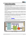
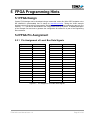
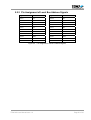
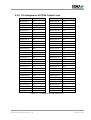
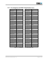
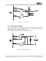
The Embedded I/O Company
TPMC630
Reconfigurable FPGA
with 64 TTL I/O / 32 Differential I/O Lines
Version 1.0
User Manual
Issue 1.6
February 2008
D76630800
TEWS TECHNOLOGIES GmbH
Am Bahnhof 7
Phone: +49-(0)4101-4058-0
25469 Halstenbek, Germany
Fax: +49-(0)4101-4058-19
www.tews.com
e-mail: [email protected]
TEWS TECHNOLOGIES LLC
9190 Double Diamond Parkway,
Suite 127, Reno, NV 89521, USA
www.tews.com
Phone: +1 (775) 850 5830
Fax: +1 (775) 201 0347
e-mail: [email protected]
TPMC630-10
64 TTL I/O Lines, XC2S300E-6 Spartan-IIE
FPGA
TPMC630-11
32 Differential I/O Lines, XC2S300E-6 SpartanIIE FPGA
TPMC630-12
32 TTL I/O and 16 Differential I/O Lines,
XC2S300E-6 Spartan-IIE FPGA
This document contains information, which is
proprietary to TEWS TECHNOLOGIES GmbH. Any
reproduction without written permission is forbidden.
TEWS TECHNOLOGIES GmbH has made any
effort to ensure that this manual is accurate and
complete. However TEWS TECHNOLOGIES GmbH
reserves the right to change the product described
in this document at any time without notice.
TPMC630-20
TEWS TECHNOLOGIES GmbH is not liable for any
damage arising out of the application or use of the
device described herein.
64 TTL I/O Lines, XC2S600E-6 Spartan-IIE
FPGA
Style Conventions
TPMC630-21
Hexadecimal characters are specified with prefix 0x,
i.e. 0x029E (that means hexadecimal value 029E).
32 Differential I/O Lines, XC2S600E-6 SpartanIIE FPGA
TPMC630-22
32 TTL I/O and 16 Differential I/O Lines,
XC2S600E-6 Spartan-IIE FPGA
For signals on hardware products, an ‚Active Low’ is
represented by the signal name with # following, i.e.
IP_RESET#.
Access terms are described as:
W
Write Only
R
Read Only
R/W
Read/Write
R/C
Read/Clear
R/S
Read/Set
©2005-2008 by TEWS TECHNOLOGIES GmbH
TPMC630 User Manual Issue 1.6
Page 2 of 46
Issue
Description
Date
1.0
First Issue
July 2005
1.1
Technical Specifications added
September 2005
1.2
Default Pull Up Voltage changed
October 2005
1.3
TTL Transceivers changed
March 2006
1.4
Pin out description for each variant
May 2006
1.5
New address TEWS LLC
September 2006
1.6
New module variants -2x
February 2008
TPMC630 User Manual Issue 1.6
Page 3 of 46
Table of Contents
1
2
3
PRODUCT DESCRIPTION ......................................................................................... 8
TECHNICAL SPECIFICATION................................................................................... 9
LOCAL SPACE ADDRESSING................................................................................ 10
3.1 PCI9030 Local Space Configuration ...........................................................................................10
3.2 FPGA Example Design Register Space ......................................................................................10
3.2.1 Output Register 0 (OUT_REG0; 0x00)...............................................................................11
3.2.2 Output Register 1 (OUT_REG1; 0x04)...............................................................................12
3.2.3 Input Register 0 (IN_REG0; 0x08)......................................................................................13
3.2.4 Input Register 1 (IN_REG1; 0x0C) .....................................................................................14
3.2.5 Output Enable Register 0 (OE_REG0; 0x10).....................................................................15
3.2.6 Output Enable Register 1 (OE_REG1; 0x14).....................................................................16
3.2.7 Interrupt Status Register (ISR; 0x18) .................................................................................17
3.2.8 Positive Edge Interrupt Enable Register (PIER; 0x1C) ......................................................17
3.2.9 Negative Edge Interrupt Enable Register (NIER; 0x20) .....................................................18
3.2.10 RAM Address Map Register (RAMR; 0x24) .....................................................................19
3.2.11 RAM Space.......................................................................................................................19
4
PCI9030 TARGET CHIP........................................................................................... 20
4.1 PCI Configuration Registers (PCR) .............................................................................................20
4.1.1 PCI9030 Header .................................................................................................................20
4.1.2 PCI Base Address Initialization ..........................................................................................21
4.2 Local Configuration Register (LCR)............................................................................................22
4.3 Configuration EEPROM ................................................................................................................23
4.4 Local Software Reset....................................................................................................................24
4.5 Local Bus .......................................................................................................................................24
5
FPGA PROGRAMMING HINTS ............................................................................... 25
5.1 FPGA Design .................................................................................................................................25
5.2 FPGA Pin Assignment ..................................................................................................................25
5.2.1 Pin Assignment of Local Bus Data Signals ........................................................................25
5.2.2 Pin Assignment of Local Bus Address Signals...................................................................26
5.2.3 Pin Assignment of Local Bus Control Signals ....................................................................27
5.2.4 Pin Assignment of Clock Signals........................................................................................27
5.2.5 Pin Assignment of FPGA Input Lines .................................................................................28
5.2.6 Pin Assignment of FPGA Output Lines ..............................................................................29
5.2.7 Pin Assignment of FPGA Output Enable Lines ..................................................................30
6
CONFIGURATION HINTS ........................................................................................ 31
6.1 Big / Little Endian..........................................................................................................................31
6.2 Clock Programming ......................................................................................................................33
7
INSTALLATION........................................................................................................ 35
7.1 Pull Up Voltage..............................................................................................................................35
7.2 I/O Interface ...................................................................................................................................35
7.2.1 TTL I/O Interface.................................................................................................................35
7.2.2 Differential I/O Interface......................................................................................................36
7.3 Back I/O Configuration .................................................................................................................37
7.4 FPGA Debug Connector ...............................................................................................................39
8
PIN ASSIGNMENT – I/O CONNECTOR .................................................................. 40
TPMC630 User Manual Issue 1.6
Page 4 of 46
8.1 Front Panel I/O Connector ...........................................................................................................40
8.1.1 Front I/O Assignment TPMC630-x0 ...................................................................................41
8.1.2 Front I/O Assignment TPMC630-x1 ...................................................................................42
8.1.3 Front I/O Assignment TPMC630-x2 ...................................................................................43
8.2 Back I/O PMC Connector..............................................................................................................44
8.2.1 Back I/O Assignment TPMC630-x0....................................................................................44
8.2.2 Back I/O Assignment TPMC630-x1....................................................................................45
8.2.3 Back I/O Assignment TPMC630-x2....................................................................................46
TPMC630 User Manual Issue 1.6
Page 5 of 46
Table of Figures
FIGURE 1-1 : BLOCK DIAGRAM......................................................................................................................8
FIGURE 2-1 : TECHNICAL SPECIFICATION...................................................................................................9
FIGURE 3-1 : PCI9030 LOCAL SPACE CONFIGURATION ..........................................................................10
FIGURE 3-2 : FPGA EXAMPLE DESIGN REGISTER SPACE ......................................................................10
FIGURE 3-3 : OUTPUT REGISTER 0 (OUT_REG0) .....................................................................................11
FIGURE 3-4 : OUTPUT REGISTER 1 (OUT_REG1) .....................................................................................12
FIGURE 3-5 : INPUT REGISTER 0 (IN_REG0)..............................................................................................13
FIGURE 3-6 : INPUT REGISTER 1 (IN_REG1)..............................................................................................14
FIGURE 3-7 : OUTPUT ENABLE REGISTER 0 (OE_REG0).........................................................................15
FIGURE 3-8 : OUTPUT ENABLE REGISTER 1 (OE_REG1).........................................................................16
FIGURE 3-9 : INTERRUPT STATUS REGISTER (ISR).................................................................................17
FIGURE 3-10: POSITIVE EDGE INTERRUPT ENABLE REGISTER (PIER) ................................................17
FIGURE 3-11: NEGATIVE EDGE INTERRUPT ENABLE REGISTER (NIER)...............................................18
FIGURE 3-12: ADDRESS MAP REGISTER (RAMR).....................................................................................19
FIGURE 4-1 : DEFAULT PCI9030 HEADER ..................................................................................................20
FIGURE 4-2 : PCI9030 PCI BASE ADDRESS USAGE..................................................................................21
FIGURE 4-3 : PCI9030 LOCAL CONFIGURATION REGISTER ....................................................................22
FIGURE 4-4 : CONFIGURATION EEPROM TPMC630 .................................................................................23
FIGURE 4-5 : DEFAULT VALUES OF SPACE 0 REGION DESCRIPTOR....................................................24
FIGURE 5-1 : PIN ASSIGNMENT LOCAL BUS DATA SIGNALS ..................................................................25
FIGURE 5-2 : PIN ASSIGNMENT LOCAL BUS ADDRESS SIGNALS ..........................................................26
FIGURE 5-3 : PIN ASSIGNMENT LOCAL BUS CONTROL SIGNALS ..........................................................27
FIGURE 5-4 : PIN ASSIGNMENT CLOCK INPUTS .......................................................................................27
FIGURE 5-5 : PIN ASSIGNMENT FPGA INPUT LINES.................................................................................28
FIGURE 5-6 : PIN ASSIGNMENT FPGA OUTPUT LINES.............................................................................29
FIGURE 5-7 : PIN ASSIGNMENT FPGA OUTPUT ENABLE LINES .............................................................30
FIGURE 6-1 : LOCAL BUS LITTLE/BIG ENDIAN...........................................................................................31
FIGURE 6-2 : DEFAULT VALUES OF CLOCK OUTPUTS (AT DELIVERY) .................................................33
FIGURE 6-3 : DEFAULT REGISTER VALUES (AT DELIVERY)....................................................................34
FIGURE 7-1 : PULL UP VOLTAGE JUMPER SETTING ................................................................................35
FIGURE 7-2 : TTL I/O INTERFACE ................................................................................................................36
FIGURE 7-3 : DIFFERENTIAL I/O INTERFACE.............................................................................................36
FIGURE 7-4 : JUMPER POSITIONS FOR GROUND OPTION......................................................................37
FIGURE 7-5 : JUMPER POSITIONS FOR BACK I/O OPTIONS....................................................................38
FIGURE 7-6 : DEBUG CONNECTOR (BOTTOM VIEW) ...............................................................................39
FIGURE 8-1 : FRONT PANEL I/O CONNECTOR NUMBERING ...................................................................40
FIGURE 8-2 : PIN ASSIGNMENT FRONT I/O CONNECTOR TPMC630-X0 ................................................41
FIGURE 8-3 : PIN ASSIGNMENT FRONT I/O CONNECTOR TPMC630-X1 ................................................42
FIGURE 8-4 : PIN ASSIGNMENT FRONT I/O CONNECTOR TPMC630-X2 ................................................43
FIGURE 8-5 : PIN ASSIGNMENT P14 I/O CONNECTOR TPMC630-X0 ......................................................44
TPMC630 User Manual Issue 1.6
Page 6 of 46
FIGURE 8-6 : PIN ASSIGNMENT P14 I/O CONNECTOR TPMC630-X1 ......................................................45
FIGURE 8-7 : PIN ASSIGNMENT P14 I/O CONNECTOR TPMC630-X2 ......................................................46
TPMC630 User Manual Issue 1.6
Page 7 of 46
1 Product Description
The TPMC630 is a standard single-width 32 bit PMC module providing a user configurable FPGA with
300,000 (TPMC630-1x) or 600,000 (TPMC630-2x) system gates. All local signals from the PCI
controller are routed to the FPGA.
The TPMC630-x0 has 64 ESD-protected TTL lines; the TPMC630-x1 provides 32 differential I/O lines
using EIA-422 / EIA-485 compatible, ESD-protected line transceivers. The TPMC630-x2 provides 32
TTL and 16 differential I/Os. All lines are individually programmable as input, output or tri-state. The
receivers are always enabled, which allows determining the state of each I/O line at any time. This can
be used as read back function for lines configured as outputs. Each TTL I/O line has a pull-up resistor.
The pull-up voltage is selectable to be either +3.3V or +5V. The differential I/O lines are terminated by
120Ω resistors.
The FPGA is configured by a serial Flash. The Flash device is in-system programmable via driver
software over the PCI bus. An in-circuit debugging option is available via an optionally mountable
JTAG header (on the backside of the board) for readback and real-time debugging of the FPGA
design (using Xilinx “ChipScope”).
A programmable clock generator provides up to six different clock output frequencies between
200 kHz and 166 MHz. All outputs are available at the FPGA; one clock source is in addition used as
the local clock signal for the PCI controller. The clock generator settings are stored in an EEPROM
and can be changed by the driver software through the PCI Target Controller.
The configuration EEPROM of the PCI Target Controller can also be modified by the driver software,
to adapt address spaces etc.
User applications can be developed using the design software ISE WebPACK which can be
downloaded free of charge from www.xilinx.com.
The TPMC630 provides front panel I/O via a HD68 SCSI-3 type connector and rear panel I/O via P14.
P14
Programmable
Clocks
Serial
Flash
XILINX FPGA
SPARTAN IIE
XC2S300 E
(TPMC630-1x)
or XC2S600E
(TPMC630-2x)
PCI
Controller
P12
P12
64 x TTL I/O
Drivers
(TPMC630-10)
or 32 x
Differential
Drivers
(TPMC630-11)
or
32 x TTL I/O
and 16 x
Differential
Drivers
(TPMC630-12)
P11
HD68 Connector
For First Time Users the Engineering Documentation is recommended, it includes schematics, data
sheets of the components and well documented sample VHDL source code.
JTAG Header
Figure 1-1 : Block Diagram
TPMC630 User Manual Issue 1.6
Page 8 of 46
2 Technical Specification
PMC Interface
Mechanical Interface
PCI Mezzanine Card (PMC) Interface
Single Size
Electrical Interface
PCI Rev. 2.1 compliant
33 MHz / 32 bit PCI
3.3V and 5V PCI Signaling Voltage
On Board Devices
PCI Target Chip
PCI9030 (PLX Technology)
Local Control Logic
TPMC630-1x: FPGA Spartan-IIE XC2S300E-6 FG456 I (Xilinx)
TPMC630-2x: FPGA Spartan-IIE XC2S600E-6 FG456 I (Xilinx)
TTL Line Transceivers
74LVT126
I/O Interface
Number of Channels
64 TTL I/O (TPMC630-x0),
32 differential I/O (TPMC630-x1) or
32 TTL I/O and 16 differential I/O (TPMC630-x2)
TTL signaling voltage level (maximum current:+/-32 mA)
or EIA-422/-485 signaling level
I/O Connectors
Front I/O HD68 SCSI-3 type Connector
(AMP 787082-7 or compatible)
PMC P14 I/O (64 pin Mezzanine Connector)
Physical Data
Power Requirements
(with Example Design)
TPMC630-x0: 160mA typical (no load) @ +3.3V DC
TPMC630-x1: 110mA typical (no load) @ +3.3V DC
TPMC630-x2: 120mA typical (no load) @ +3.3V DC
10mA typical @ +5V DC (TPMC630-x0, when used as pull up
voltage)
(+5V DC not used on TPMC630-x1)
10mA typical @ +5V DC (TPMC630-x2, when used as pull up
voltage)
Temperature Range
Operating
Storage
-40°C to +85°C
-40°C to +85°C
MTBF
TPMC630-x0: 407000 h
TPMC630-x1: 451000 h
TPMC630-x2: 428000 h
Humidity
5 – 95 % non-condensing
Weight
80 g
Figure 2-1 : Technical Specification
TPMC630 User Manual Issue 1.6
Page 9 of 46
3 Local Space Addressing
3.1 PCI9030 Local Space Configuration
The local on board addressable regions are accessed from the PCI side by using the PCI9030 local
spaces.
PCI9030
Local
Space
PCI9030
PCI Base Address
(Offset in PCI
Configuration
Space)
PCI
Space
Mapping
Size
(Byte)
Port
Width
(Bit)
Endian
Mode
Description
0
2 (0x18)
MEM
16 M
32
BIG
FPGA Example
Design
Register Space
1
3 (0x1C)
-
-
-
-
Not Used
2
4 (0x20)
-
-
-
-
Not Used
3
5 (0x24)
-
-
-
-
Not Used
Figure 3-1 : PCI9030 Local Space Configuration
3.2 FPGA Example Design Register Space
The TPMC630 is delivered with a FPGA example design in the configuration memory.
PCI Base Address:
PCI9030 PCI Base Address 2 (Offset 0x18 in PCI Configuration Space).
Offset to PCI
Base Address 2
Register Name
Size
(Bit)
0x00
OUTPUT REGISTER 0 (OUT_REG0)
32
0x04
OUTPUT REGISTER 1 (OUT_REG1)
32
0x08
INPUT REGISTER 0 (IN_REG0)
32
0x0C
INPUT REGISTER 1 (IN_REG1)
32
0x10
OUTPUT ENABLE REGISTER 0 (OE_REG0)
32
0x14
OUTPUT ENABLE REGISTER 1 (OE_REG1)
32
0x18
INTERRUPT STATUS REGISTER (ISR)
32
0x1C
POSITIVE EDGE INTERRUPT ENABLE REGISTER
(PIER)
32
0x20
NEGATIVE EDGE INTERRUPT ENABLE REGISTER
(NIER)
32
0x24
RAM ADDRESS MAP REGISTER (RAMR)
32
0x28 .. 0xFFFFFF
256 x 32 bit RAM Space
32
Figure 3-2 : FPGA Example Design Register Space
TPMC630 User Manual Issue 1.6
Page 10 of 46
3.2.1 Output Register 0 (OUT_REG0; 0x00)
Bit
Symbol
31
OUT_REG_BIT_31
Description
30
OUT_REG_BIT_30
29
OUT_REG_BIT_29
28
OUT_REG_BIT_28
27
OUT_REG_BIT_27
26
OUT_REG_BIT_26
25
OUT_REG_BIT_25
24
OUT_REG_BIT_24
23
OUT_REG_BIT_23
22
OUT_REG_BIT_22
21
OUT_REG_BIT_21
20
OUT_REG_BIT_20
19
OUT_REG_BIT_19
18
OUT_REG_BIT_18
17
OUT_REG_BIT_17
16
OUT_REG_BIT_16
15
OUT_REG_BIT_15
14
OUT_REG_BIT_14
13
OUT_REG_BIT_13
12
OUT_REG_BIT_12
11
OUT_REG_BIT_11
10
OUT_REG_BIT_10
9
OUT_REG_BIT_9
8
OUT_REG_BIT_8
7
OUT_REG_BIT_7
6
OUT_REG_BIT_6
5
OUT_REG_BIT_5
4
OUT_REG_BIT_4
3
OUT_REG_BIT_3
2
OUT_REG_BIT_2
1
OUT_REG_BIT_1
0
OUT_REG_BIT_0
Output Port Bit 31-0 Data
(see notes below)
Access
Reset Value
R/W
0
Figure 3-3 : Output Register 0 (OUT_REG0)
TPMC630-x0: Output Port Bits 0 - 31 are written to IO_0 - IO_31 (TTL)
TPMC630-x1: Output Port Bits 0 - 31 are written to IO_0A/B - IO_31A/B (Differential)
TPMC630-x2: Output Port Bits 0 - 15 are written to IO_0A/B - IO_15A/B (Differential)
Output Port Bits 16 - 31 are not used
TPMC630 User Manual Issue 1.6
Page 11 of 46
3.2.2 Output Register 1 (OUT_REG1; 0x04)
Bit
Symbol
Description
63
OUT_REG_BIT_63
62
OUT_REG_BIT_62
61
OUT_REG_BIT_61
60
OUT_REG_BIT_60
59
OUT_REG_BIT_59
58
OUT_REG_BIT_58
57
OUT_REG_BIT_57
56
OUT_REG_BIT_56
55
OUT_REG_BIT_55
54
OUT_REG_BIT_54
53
OUT_REG_BIT_53
52
OUT_REG_BIT_52
51
OUT_REG_BIT_51
50
OUT_REG_BIT_50
49
OUT_REG_BIT_49
48
OUT_REG_BIT_48
47
OUT_REG_BIT_47
46
OUT_REG_BIT_46
45
OUT_REG_BIT_45
44
OUT_REG_BIT_44
43
OUT_REG_BIT_43
42
OUT_REG_BIT_42
41
OUT_REG_BIT_41
40
OUT_REG_BIT_40
39
OUT_REG_BIT_39
38
OUT_REG_BIT_38
37
OUT_REG_BIT_37
36
OUT_REG_BIT_36
35
OUT_REG_BIT_35
34
OUT_REG_BIT_34
33
OUT_REG_BIT_33
32
OUT_REG_BIT_32
Output Port Bit 63-32 Data
(see notes below)
Access
Reset
Value
R/W
0
Figure 3-4 : Output Register 1 (OUT_REG1)
TPMC630-x0: Output Port Bits 32 - 63 are written to IO_32 - IO_63 (TTL)
TPMC630-x1: Output Port Bits 32 - 63 are not used
TPMC630-x2: Output Port Bits 32 - 63 are written to IO_32 - IO_63 (TTL)
TPMC630 User Manual Issue 1.6
Page 12 of 46
3.2.3 Input Register 0 (IN_REG0; 0x08)
Read directly from the I/O lines 31 to 0.
Bit
Symbol
31
IN_REG_BIT_31
30
IN_REG_BIT_30
29
IN_REG_BIT_29
28
IN_REG_BIT_28
27
IN_REG_BIT_27
26
IN_REG_BIT_26
25
IN_REG_BIT_25
24
IN_REG_BIT_24
23
IN_REG_BIT_23
22
IN_REG_BIT_22
21
IN_REG_BIT_21
20
IN_REG_BIT_20
19
IN_REG_BIT_19
18
IN_REG_BIT_18
17
IN_REG_BIT_17
16
IN_REG_BIT_16
15
IN_REG_BIT_15
14
IN_REG_BIT_14
13
IN_REG_BIT_13
12
IN_REG_BIT_12
11
IN_REG_BIT_11
10
IN_REG_BIT_10
9
IN_REG_BIT_9
8
IN_REG_BIT_8
7
IN_REG_BIT_7
6
IN_REG_BIT_6
5
IN_REG_BIT_5
4
IN_REG_BIT_4
3
IN_REG_BIT_3
2
IN_REG_BIT_2
1
IN_REG_BIT_1
0
IN_REG_BIT_0
Description
Input Port Bit 31-0 Data
(see notes below)
Access
Reset Value
R
-
Figure 3-5 : Input Register 0 (IN_REG0)
TPMC630-x0: Input Port Bits 0 - 31 are read from IO_0 - IO_31 (TTL)
TPMC630-x1: Input Port Bits 0 - 31 are read from IO_0A/B - IO_31A/B (Differential)
TPMC630-x2: Input Port Bits 0 - 15 are read from IO_0A/B - IO_15A/B (Differential)
Input Port Bits 16 - 31 are not used
TPMC630 User Manual Issue 1.6
Page 13 of 46
3.2.4 Input Register 1 (IN_REG1; 0x0C)
Read directly from the I/O lines 63 to 32.
Bit
Symbol
63
IN_REG_BIT_63
62
IN_REG_BIT_62
61
IN_REG_BIT_61
60
IN_REG_BIT_60
59
IN_REG_BIT_59
58
IN_REG_BIT_58
57
IN_REG_BIT_57
56
IN_REG_BIT_56
55
IN_REG_BIT_55
54
IN_REG_BIT_54
53
IN_REG_BIT_53
52
IN_REG_BIT_52
51
IN_REG_BIT_51
50
IN_REG_BIT_50
49
IN_REG_BIT_49
48
IN_REG_BIT_48
47
IN_REG_BIT_47
46
IN_REG_BIT_46
45
IN_REG_BIT_45
44
IN_REG_BIT_44
43
IN_REG_BIT_43
42
IN_REG_BIT_42
41
IN_REG_BIT_41
40
IN_REG_BIT_40
39
IN_REG_BIT_39
38
IN_REG_BIT_38
37
IN_REG_BIT_37
36
IN_REG_BIT_36
35
IN_REG_BIT_35
34
IN_REG_BIT_34
33
IN_REG_BIT_33
32
IN_REG_BIT_32
Description
Input Port Bit 63-32 Data
(see notes below)
Access
Reset
Value
R
-
Figure 3-6 : Input Register 1 (IN_REG1)
TPMC630-x0: Input Port Bits 32 - 63 are read from IO_32 - IO_63 (TTL)
TPMC630-x1: Input Port Bits 32 - 63 are not used
TPMC630-x2: Input Port Bits 32 - 63 are read from IO_32 - IO_63 (TTL)
TPMC630 User Manual Issue 1.6
Page 14 of 46
3.2.5 Output Enable Register 0 (OE_REG0; 0x10)
Bit
Symbol
Description
31
OE_REG_BIT_31
30
OE_REG_BIT_30
29
OE_REG_BIT_29
28
OE_REG_BIT_28
27
OE_REG_BIT_27
26
OE_REG_BIT_26
25
OE_REG_BIT_25
24
OE_REG_BIT_24
23
OE_REG_BIT_23
22
OE_REG_BIT_22
21
OE_REG_BIT_21
20
OE_REG_BIT_20
19
OE_REG_BIT_19
18
OE_REG_BIT_18
17
OE_REG_BIT_17
16
OE_REG_BIT_16
15
OE_REG_BIT_15
14
OE_REG_BIT_14
13
OE_REG_BIT_13
12
OE_REG_BIT_12
11
OE_REG_BIT_11
10
OE_REG_BIT_10
9
OE_REG_BIT_9
8
OE_REG_BIT_8
7
OE_REG_BIT_7
6
OE_REG_BIT_6
5
OE_REG_BIT_5
4
OE_REG_BIT_4
3
OE_REG_BIT_3
2
OE_REG_BIT_2
1
OE_REG_BIT_1
0
OE_REG_BIT_0
Access
Reset
Value
R/W
0
Output Enable Bit 31-0
(see notes below)
0: disables the output transceiver
1: enables the output transceiver
Figure 3-7 : Output Enable Register 0 (OE_REG0)
TPMC630-x0: Output Enable Bits 0 - 31 control Output 0 – Output 31 (TTL)
TPMC630-x1: Output Enable Bits 0 - 31 control Output 0 – Output 31 (Differential)
TPMC630-x2: Output Enable Bits 0 - 15 control Output 0 – Output 15 (Differential)
Output Enable Bits 16 - 31 are not used
TPMC630 User Manual Issue 1.6
Page 15 of 46
3.2.6 Output Enable Register 1 (OE_REG1; 0x14)
Bit
Symbol
Description
63
OE_REG_BIT_63
62
OE_REG_BIT_62
61
OE_REG_BIT_61
60
OE_REG_BIT_60
59
OE_REG_BIT_59
58
OE_REG_BIT_58
57
OE_REG_BIT_57
56
OE_REG_BIT_56
55
OE_REG_BIT_55
54
OE_REG_BIT_54
53
OE_REG_BIT_53
52
OE_REG_BIT_52
51
OE_REG_BIT_51
50
OE_REG_BIT_50
49
OE_REG_BIT_49
48
OE_REG_BIT_48
47
OE_REG_BIT_47
46
OE_REG_BIT_46
45
OE_REG_BIT_45
44
OE_REG_BIT_44
43
OE_REG_BIT_43
42
OE_REG_BIT_42
41
OE_REG_BIT_41
40
OE_REG_BIT_40
39
OE_REG_BIT_39
38
OE_REG_BIT_38
37
OE_REG_BIT_37
36
OE_REG_BIT_36
35
OE_REG_BIT_35
34
OE_REG_BIT_34
33
OE_REG_BIT_33
32
OE_REG_BIT_32
Access
Reset
Value
R/W
0
Output Enable Bit 63-32
(see notes below)
0: disables the output transceiver
1: enables the output transceiver
Figure 3-8 : Output Enable Register 1 (OE_REG1)
TPMC630-x0: Output Enable Bits 32 - 63 control Output 32 – Output 63 (TTL)
TPMC630-x1: Output Enable Bits 32 - 63 are not used
TPMC630-x2: Output Enable Bits 32 - 63 control Output 32 – Output 63 (TTL)
TPMC630 User Manual Issue 1.6
Page 16 of 46
3.2.7 Interrupt Status Register (ISR; 0x18)
The Interrupt Status Register signals the lines on which an interrupt event occurred. The example
design supports interrupts only for line 0 to 7.
Bit
Symbol
31: 8
-
7
INT_7
6
INT_6
5
INT_5
4
INT_4
3
INT_3
2
INT_2
1
INT_1
0
INT_0
Description
Reserved (0 for reads)
Line 7-0 Interrupt Request Status
0 = no active interrupt request
1 = active interrupt request
Access
Reset
Value
-
0
R/W
0
Figure 3-9 : Interrupt Status Register (ISR)
3.2.8 Positive Edge Interrupt Enable Register (PIER; 0x1C)
Bit
Symbol
31: 8
-
Description
Reserved (0 for reads)
7
PIE_7
6
PIE _6
5
PIE _5
4
PIE _4
3
PIE _3
2
PIE _2
1
PIE _1
0
PIE _0
Line 7-0 Rising Edge Interrupt Enable
0 = disabled
1 = enabled
Access
Reset
Value
-
0
R/W
0
Figure 3-10: Positive Edge Interrupt Enable Register (PIER)
TPMC630 User Manual Issue 1.6
Page 17 of 46
3.2.9 Negative Edge Interrupt Enable Register (NIER; 0x20)
Bit
Symbol
31: 8
-
7
NIE_7
6
NIE _6
5
NIE _5
4
NIE _4
3
NIE _3
2
NIE _2
1
NIE _1
0
NIE _0
Description
Reserved (0 for reads)
Line 7-0 Falling Edge Interrupt Enable
0 = disabled
1 = enabled
Access
Reset
Value
-
0
R/W
0
Figure 3-11: Negative Edge Interrupt Enable Register (NIER)
TPMC630 User Manual Issue 1.6
Page 18 of 46
3.2.10 RAM Address Map Register (RAMR; 0x24)
The RAM Address Map Register determines at which address the 256 x 32 bit RAM space begins,
within the 16 MByte address space. If RAMR is set to 0x0, the addresses from 0x0 to 0x24 are
occupied by the registers. Only 32 bit accesses are possible.
Description
Access
Reset
Value
-
0
Bit
Symbol
31:24
-
23
RAM_ADD_MAP_BIT_23
0
22
RAM_ADD_MAP_BIT_22
0
21
RAM_ADD_MAP_BIT_21
0
20
RAM_ADD_MAP_BIT_20
0
19
RAM_ADD_MAP_BIT_19
0
18
RAM_ADD_MAP_BIT_18
0
17
RAM_ADD_MAP_BIT_17
16
RAM_ADD_MAP_BIT_16
15
RAM_ADD_MAP_BIT_15
0
14
RAM_ADD_MAP_BIT_14
0
13
RAM_ADD_MAP_BIT_13
0
12
RAM_ADD_MAP_BIT_12
0
11
RAM_ADD_MAP_BIT_11
0
10
RAM_ADD_MAP_BIT_10
1
9:0
-
Reserved (0 for reads)
Address Map Bit 23 - 10
Reserved (0 for reads)
R/W
-
0
0
0
Figure 3-12: Address Map Register (RAMR)
3.2.11 RAM Space
There is a 256 x 32 bit RAM space available; it is accessed if the address bits match to the content of
the RAM Address Map Register (See Description of RAMR). Only 32 bit accesses are possible.
TPMC630 User Manual Issue 1.6
Page 19 of 46
4 PCI9030 Target Chip
4.1 PCI Configuration Registers (PCR)
4.1.1 PCI9030 Header
PCI CFG
Register
Address
Write ‘0’ to all unused (Reserved) bits
31
24
23
16
15
PCI
Initial Values
writeable (Hex Values)
8
7
0
0x00
Device ID
Vendor ID
N
0276 1498
0x04
Status
Command
Y
0280 0000
Revision ID
N
118000 00
Cache Line
Size
Y[7:0]
00 00 00 00
0x08
0x0C
Class Code
BIST
Header Type
PCI Latency
Timer
0x10
PCI Base Address 0 for MEM Mapped Config. Registers
Y
FFFFFF80
0x14
PCI Base Address 1 for I/O Mapped Config. Registers
Y
FFFFFF81
0x18
PCI Base Address 2 for Local Address Space 0
Y
FF000000
0x1C
PCI Base Address 3 for Local Address Space 1
Y
00000000
0x20
PCI Base Address 4 for Local Address Space 2
Y
00000000
0x24
PCI Base Address 5 for Local Address Space 3
Y
00000000
0x28
PCI CardBus Information Structure Pointer
N
00000000
0x2C
Subsystem ID
0x30
PCI Base Address for Local Expansion ROM
0x34
Reserved
0x38
0x3C
Subsystem Vendor ID
Max_Lat
0x40
Min_Gnt
PM Cap.
0x44
PM Data
PM CSR EXT
0x48
Reserved
HS CSR
0x4C
New Cap. Ptr.
Reserved
VPD Address
0x50
N
s.b.
1498
Y
00000000
N
000000 40
N
00000000
00 00 01 00
Interrupt Pin
Interrupt Line
Y[7:0]
PM Nxt Cap.
PM Cap. ID
N
4801 00 01
Y
00 00 0000
PM CSR
HS Nxt Cap.
HS Cap. ID
Y[23:16]
00 00 00 06
VPD Nxt Cap.
VPD Cap. ID
Y[31:16]
0000 00 03
Y
00000000
VPD Data
Figure 4-1 : Default PCI9030 Header
Subsystem-ID Value (Offset 0x2E): TPMC630-10
0x000A
TPMC630-11
0x000B
TPMC630-12
0x000C
TPMC630-20
0x0014
TPMC630-21
0x0015
TPMC630-22
0x0016
TPMC630 User Manual Issue 1.6
Page 20 of 46
4.1.2 PCI Base Address Initialization
PCI Base Address Initialization is scope of the PCI host software.
PCI9030 PCI Base Address Initialization:
1. Write 0xFFFF_FFFF to the PCI9030 PCI Base Address Register.
2. Read back the PCI9030 PCI Base Address Register.
3. For PCI Base Address Registers 0:5, check bit 0 for PCI Address Space.
Bit 0 = '0' requires PCI Memory Space mapping
Bit 0 = '1' requires PCI I/O Space mapping
For the PCI Expansion ROM Base Address Register, check bit 0 for usage.
Bit 0 = ‘0’: Expansion ROM not used
Bit 0 = ‘1’: Expansion ROM used
4. For PCI I/O Space mapping, starting at bit location 2, the first bit set determines the size of the
required PCI I/O Space size.
For PCI Memory Space mapping, starting at bit location 4, the first bit set to '1' determines the size
of the required PCI Memory Space size.
For PCI Expansion ROM mapping, starting at bit location 11, the first bit set to '1' determines the
required PCI Expansion ROM size.
For example, if bit 5 of a PCI Base Address Register is detected as the first bit set to ‘1’, the
PCI9030 is requesting a 32 byte space (address bits 4:0 are not part of base address decoding).
5. Determine the base address and write the base address to the PCI9030 PCI Base Address
Register. For PCI Memory Space mapping the mapped address region must comply with the
definition of bits 3:1 of the PCI9030 PCI Base Address Register.
After programming the PCI9030 PCI Base Address Registers, the software must enable the
PCI9030 for PCI I/O and/or PCI Memory Space access in the PCI9030 PCI Command Register
(Offset 0x04). To enable PCI I/O Space access to the PCI9030, set bit 0 to '1'. To enable PCI
Memory Space access to the PCI9030, set bit 1 to '1'.
Offset in Config.
Description
Usage
0x10
PCI9030 LCR’s MEM
Used
0x14
PCI9030 LCR’s I/O
Used
0x18
PCI9030 Local Space 0
Used
0x1C
PCI9030 Local Space 1
Not used
0x30
Expansion ROM
Not used
Figure 4-2 : PCI9030 PCI Base Address Usage
TPMC630 User Manual Issue 1.6
Page 21 of 46
4.2 Local Configuration Register (LCR)
After reset, the PCI9030 Local Configuration Registers are loaded from the on board serial
configuration EEPROM.
The PCI base address for the PCI9030 Local Configuration Registers is PCI9030 PCI Base
Address 0 (PCI Memory Space) (Offset 0x10 in the PCI9030 PCI Configuration Register Space)
or PCI9030 PCI Base Address 1 (PCI I/O Space) (Offset 0x14 in the PCI9030 PCI Configuration
Register Space).
Please be very careful when changing any hardware dependent bit settings in the PCI9030
Local Configuration Registers.
Offset from
PCI Base
Address
Register
Default Value
Description
0x00
Local Address Space 0 Range
0x0F00_0000
Defines size of space
0x04
Local Address Space 1 Range
0x0000_0000
0x08
Local Address Space 2 Range
0x0000_0000
0x0C
Local Address Space 3 Range
0x0000_0000
0x10
Local Exp. ROM Range
0x0000_0000
0x14
Local Re-map Register Space 0
0x0000_0001
0x18
Local Re-map Register Space 1
0x0000_0000
0x1C
Local Re-map Register Space 2
0x0000_0000
0x20
Local Re-map Register Space 3
0x0000_0000
0x24
Local Re-map Register ROM
0x0000_0000
0x28
Local Address Space 0 Descriptor
0x1581_20A0
0x2C
Local Address Space 1 Descriptor
0x0000_0000
0x30
Local Address Space 2 Descriptor
0x0000_0000
0x34
Local Address Space 3 Descriptor
0x0000_0000
0x38
Local Exp. ROM Descriptor
0x0000_0000
0x3C
Chip Select 0 Base Address
0x0080_0001
0x40
Chip Select 1 Base Address
0x0000_0002
0x44
Chip Select 2 Base Address
0x0000_0002
0x48
Chip Select 3 Base Address
0x0000_0002
0x4C
Interrupt Control/Status
0x0041
0x4E
EEPROM Write Protect Boundary
0x0030
0x50
Miscellaneous Control Register
0x0078_0000
0x54
General Purpose I/O Control
0x0000_0240
0x70
Hidden1 Power Management data
select
0x0000_0000
0x74
Hidden 2 Power Management data
scale
0x0000_0000
Defines local address of space
Defines properties of space
Defines range for Chip Select
Figure 4-3 : PCI9030 Local Configuration Register
TPMC630 User Manual Issue 1.6
Page 22 of 46
4.3 Configuration EEPROM
After power-on or PCI reset, the PCI9030 loads initial configuration register data from the on board
configuration EEPROM.
The configuration EEPROM contains the following configuration data:
• Address 0x00 to 0x27 : PCI9030 PCI Configuration Register Values
• Address 0x28 to 0x87 : PCI9030 Local Configuration Register Values
• Address 0x88 to 0xFF : Reserved
See the PCI9030 Manual for more information.
The following table shows the default content of the EEPROM.
Address
Offset
0x00
0x02
0x04
0x06
0x08
0x0A
0x0C
0x0E
0x00
0x0276
0x1498
0x0280
0x0000
0x1180
0x0000
s.b.
0x1498
0x10
0x0000
0x0040
0x0000
0x0100
0x4801
0x0001
0x0000
0x0000
0x20
0x0000
0x0006
0x0000
0x0003
0x0F00
0x0000
0x0000
0x0000
0x30
0x0000
0x0000
0x0000
0x0000
0x0000
0x0000
0x0000
0x0001
0x40
0x0000
0x0000
0x0000
0x0000
0x0000
0x0000
0x0000
0x0000
0x50
0x1581
0x20A0
0x0000
0x0000
0x0000
0x0000
0x0000
0x0000
0x60
0x0000
0x0000
0x0080
0x0001
0x0000
0x0002
0x0000
0x0002
0x70
0x0000
0x0002
0x0030
0x0041
0x0078
0x0000
0x0000
0x0240
0x80
0x0000
0x0000
0x0000
0x0000
0xFFFF
0xFFFF
0xFFFF
0xFFFF
0x90
0xFFFF
0xFFFF
0xFFFF
0xFFFF
0xFFFF
0xFFFF
0xFFFF
0xFFFF
0xA0
0xFFFF
0xFFFF
0xFFFF
0xFFFF
0xFFFF
0xFFFF
0xFFFF
0xFFFF
0xB0
0xFFFF
0xFFFF
0xFFFF
0xFFFF
0xFFFF
0xFFFF
0xFFFF
0xFFFF
0xC0
0xFFFF
0xFFFF
0xFFFF
0xFFFF
0xFFFF
0xFFFF
0xFFFF
0xFFFF
0xD0
0xFFFF
0xFFFF
0xFFFF
0xFFFF
0xFFFF
0xFFFF
0xFFFF
0xFFFF
0xE0
0xFFFF
0xFFFF
0xFFFF
0xFFFF
0xFFFF
0xFFFF
0xFFFF
0xFFFF
0xF0
0xFFFF
0xFFFF
0xFFFF
0xFFFF
0xFFFF
0xFFFF
0xFFFF
0xFFFF
Figure 4-4 : Configuration EEPROM TPMC630
Subsystem-ID Value (Offset 0x0C): TPMC630-10
0x000A
TPMC630-11
0x000B
TPMC630-12
0x000C
TPMC630-20
0x0014
TPMC630-21
0x0015
TPMC630-22
0x0016
Highlighted values can be modified by the driver software.
TPMC630 User Manual Issue 1.6
Page 23 of 46
4.4 Local Software Reset
The PCI9030 Local Reset Output LRESETo# is used to reset the on board local logic.
The PCI9030 local reset is active during PCI reset or if the PCI Adapter Software Reset bit is set in the
PCI9030 local configuration register CNTRL (offset 0x50).
CNTRL[30] PCI Adapter Software Reset:
Value of ‘1’ resets the PCI9030 and issues a reset to the Local Bus (LRESETo# asserted). The
PCI9030 remains in this reset condition until the PCI Host clears this bit. The contents of the PCI9030
PCI and Local Configuration Registers are not reset. The PCI9030 PCI Interface is not reset.
4.5 Local Bus
The PCI9030 Local Bus is a 32 bit non-multiplexed bus. Many parameters of the local interface can be
configured, such as wait states, delays, etc. (see PCI9030 Data Book).
The default values of the Local Address Space 0 Bus Region Descriptor (LAS0BRD; 0x28) for the
example design are:
Default
Value
Bit
Description
Local Address Space 0 Burst Enable
0
Bursting disabled
Local Address Space 0 READY# Input Enable
0
READY# input disabled
Local Address Space 0 BTERM# Input Enable
0
BTERM# input disabled
Prefetch Count
00
Do not prefetch (disable)
Prefetch Counter Enable
1
Set to 1 (disabled by Prefetch Count=0)
NRAD Wait States
00010
NRDD Wait States
00
Read Address to Data wait states
Read Data to Data wait states
NXDA Wait States
01
NWAD Wait States
00010
Read/Write Data to Address wait states
NWDD Wait States
00
Local Address Space 0 Local Bus Width
10
32 bit bus width
Byte Ordering
1
Big Endian
Big Endian Byte Lane Mode
0
Use lanes [15:0], [7:0] in non 32 bit modes
Read Strobe Delay
01
Delay until assertion of RD#
Write Strobe Delay
01
Delay until assertion of WR#
Write Cycle Hold
00
Hold data after
Write Address to Data wait states
Write Data to Data wait states
Figure 4-5 : Default values of Space 0 Region Descriptor
TPMC630 User Manual Issue 1.6
Page 24 of 46
5 FPGA Programming Hints
5.1 FPGA Design
Custom FPGA designs can be developed using a commercial version like Xilinx ISE Foundation or the
ISE WebPACK, downloadable free of charge at www.xilinx.com/ise. Taking the VHDL example
provided with the Engineering Documentation would be a good basis. After implementing the logic, the
resulting .xsvf file can be downloaded to the configuration flash by the driver. A detailed description
of the example files and how to generate the configuration bit stream file is part of the Engineering
Documentation.
5.2 FPGA Pin Assignment
5.2.1 Pin Assignment of Local Bus Data Signals
Signal
Pin
Signal
Pin
LD 0
W7
LD 16
AB13
LD 1
V7
LD 17
Y11
LD 2
AA10
LD 18
P6
LD 3
P5
LD 19
N5
LD 4
Y10
LD 20
L3
LD 5
M4
LD 21
N4
LD 6
W10
LD 22
M3
LD 7
K3
LD 23
Y9
LD 8
M5
LD 24
AB10
LD 9
N6
LD 25
AA9
LD 10
V11
LD 26
P4
LD 11
AB15
LD 27
T5
LD 12
AA14
LD 28
AB9
LD 13
U10
LD 29
V6
LD 14
W11
LD 30
Y7
LD 15
U9
LD 31
AB8
Figure 5-1 : Pin Assignment Local Bus Data Signals
TPMC630 User Manual Issue 1.6
Page 25 of 46
5.2.2 Pin Assignment of Local Bus Address Signals
Signal
Pin
Signal
Pin
LA 2
P3
LA 13
V4
LA 3
W6
LA 14
AB5
LA 4
T4
LA 15
R3
LA 5
AA7
LA 16
T3
LA 6
U4
LA 17
U3
LA 7
AB7
LA 18
V3
LA 8
AA6
LA 19
W3
LA 9
W5
LA 20
AB3
LA 10
AB6
LA 21
AA3
LA 11
Y5
LA 22
W2
LA 12
AA5
LA 23
V2
Figure 5-2 : Pin Assignment Local Bus Address Signals
TPMC630 User Manual Issue 1.6
Page 26 of 46
5.2.3 Pin Assignment of Local Bus Control Signals
Signal
Pin
Description
LRESET#
T2
Local Reset
LRD#
W1
Local Read
LWR#
P1
Local Write
LADS#
L1
Local Address Strobe
LBE0#
AA18
Local Byte Enable 0
LBE1#
AB16
Local Byte Enable 1
LBE2#
Y13
Local Byte Enable 2
LBE3#
AA11
Local Byte Enable 3
LCS0#
R1
Local Chip Select 0
LCS1#
R2
Local Chip Select 1
LCS2#
L2
Local Chip Select 2
LCS3#
U1
Local Chip Select 3
LINT1#
T1
Local Interrupt 1
LINT2#
U2
Local Interrupt 2
LBLAST#
M1
Local Burst Last
LRDY#
N2
Local Ready
LW_R#
Y2
Local Write/Read (low active for reads,
high for writes)
LBTERM#
P2
Local Burst Terminate
Figure 5-3 : Pin Assignment Local Bus Control Signals
In the VHDL example code, low active signals have an ‘n’ as last character, instead of the ‘#’.
5.2.4 Pin Assignment of Clock Signals
Signal
Pin
Description
Default values
BCLK
AA12
Buffered PCI Clock
PCI Clock from Carrier
CLK1
AB12
CLK1 Output of Clock Generator
50 MHz
CLK2
A11
CLK2 Output of Clock Generator
20 MHz
CLK3
C11
CLK3 Output of Clock Generator
10 MHz
CLK4
AB21
CLK4 Output of Clock Generator
1 MHz
CLK5
W22
CLK5 Output of Clock Generator
200 kHz
CLK6
U21
CLK6 Output of Clock Generator
(Off)
Figure 5-4 : Pin Assignment Clock Inputs
TPMC630 User Manual Issue 1.6
Page 27 of 46
5.2.5 Pin Assignment of FPGA Input Lines
Signal
Pin
Signal
Pin
FPGA_IN 0
F1
FPGA_IN 32
E19
FPGA_IN 1
C1
FPGA_IN 33
E20
FPGA_IN 2
D2
FPGA_IN 34
F11
FPGA_IN 3
D3
FPGA_IN 35
F19
FPGA_IN 4
G3
FPGA_IN 36
N18
FPGA_IN 5
C5
FPGA_IN 37
N19
FPGA_IN 6
F5
FPGA_IN 38
J4
FPGA_IN 7
B7
FPGA_IN 39
M18
FPGA_IN 8
A9
FPGA_IN 40
M20
FPGA_IN 9
C8
FPGA_IN 41
J5
FPGA_IN 10
A14
FPGA_IN 42
L18
FPGA_IN 11
C12
FPGA_IN 43
H4
FPGA_IN 12
C9
FPGA_IN 44
U13
FPGA_IN 13
B10
FPGA_IN 45
V15
FPGA_IN 14
C15
FPGA_IN 46
U14
FPGA_IN 15
D15
FPGA_IN 47
V16
FPGA_IN 16
E10
FPGA_IN 48
V20
FPGA_IN 17
E13
FPGA_IN 49
L6
FPGA_IN 18
M19
FPGA_IN 50
U20
FPGA_IN 19
L20
FPGA_IN 51
T18
FPGA_IN 20
A15
FPGA_IN 52
AA13
FPGA_IN 21
B14
FPGA_IN 53
V12
FPGA_IN 22
L22
FPGA_IN 54
AB17
FPGA_IN 23
K22
FPGA_IN 55
U12
FPGA_IN 24
J22
FPGA_IN 56
AB18
FPGA_IN 25
A18
FPGA_IN 57
Y16
FPGA_IN 26
R21
FPGA_IN 58
W15
FPGA_IN 27
R22
FPGA_IN 59
AB20
FPGA_IN 28
E16
FPGA_IN 60
AA8
FPGA_IN 29
E17
FPGA_IN 61
N3
FPGA_IN 30
V21
FPGA_IN 62
W9
FPGA_IN 31
V22
FPGA_IN 63
V9
Figure 5-5 : Pin Assignment FPGA Input Lines
TPMC630 User Manual Issue 1.6
Page 28 of 46
5.2.6 Pin Assignment of FPGA Output Lines
Signal
Pin
Signal
Pin
FPGA_OUT 0
E2
FPGA_OUT 32
B19
FPGA_OUT 1
E3
FPGA_OUT 33
C14
FPGA_OUT 2
B5
FPGA_OUT 34
C17
FPGA_OUT 3
B3
FPGA_OUT 35
D14
FPGA_OUT 4
A4
FPGA_OUT 36
K21
FPGA_OUT 5
F4
FPGA_OUT 37
J17
FPGA_OUT 6
A6
FPGA_OUT 38
J19
FPGA_OUT 7
C6
FPGA_OUT 39
J20
FPGA_OUT 8
A8
FPGA_OUT 40
G5
FPGA_OUT 9
B8
FPGA_OUT 41
F9
FPGA_OUT 10
D10
FPGA_OUT 42
G18
FPGA_OUT 11
A17
FPGA_OUT 43
G20
FPGA_OUT 12
A10
FPGA_OUT 44
V17
FPGA_OUT 13
D8
FPGA_OUT 45
U18
FPGA_OUT 14
D13
FPGA_OUT 46
U19
FPGA_OUT 15
D16
FPGA_OUT 47
K4
FPGA_OUT 16
D21
FPGA_OUT 48
T20
FPGA_OUT 17
E15
FPGA_OUT 49
K5
FPGA_OUT 18
L17
FPGA_OUT 50
J3
FPGA_OUT 19
K17
FPGA_OUT 51
P18
FPGA_OUT 20
D9
FPGA_OUT 52
Y15
FPGA_OUT 21
B12
FPGA_OUT 53
W14
FPGA_OUT 22
G21
FPGA_OUT 54
AA17
FPGA_OUT 23
E21
FPGA_OUT 55
AB19
FPGA_OUT 24
F22
FPGA_OUT 56
Y17
FPGA_OUT 25
D22
FPGA_OUT 57
W16
FPGA_OUT 26
N21
FPGA_OUT 58
W17
FPGA_OUT 27
N22
FPGA_OUT 59
Y19
FPGA_OUT 28
B15
FPGA_OUT 60
W8
FPGA_OUT 29
B17
FPGA_OUT 61
V8
FPGA_OUT 30
T21
FPGA_OUT 62
V10
FPGA_OUT 31
T22
FPGA_OUT 63
AB14
Figure 5-6 : Pin Assignment FPGA Output Lines
TPMC630 User Manual Issue 1.6
Page 29 of 46
5.2.7 Pin Assignment of FPGA Output Enable Lines
Signal
Pin
Signal
Pin
FPGA_OE 0
D1
FPGA_OE 32
B18
FPGA_OE 1
A3
FPGA_OE 33
C13
FPGA_OE 2
A5
FPGA_OE 34
C16
FPGA_OE 3
F2
FPGA_OE 35
D12
FPGA_OE 4
F3
FPGA_OE 36
K18
FPGA_OE 5
B4
FPGA_OE 37
G4
FPGA_OE 6
D5
FPGA_OE 38
J18
FPGA_OE 7
B6
FPGA_OE 39
F20
FPGA_OE 8
C7
FPGA_OE 40
J21
FPGA_OE 9
D7
FPGA_OE 41
H18
FPGA_OE 10
B13
FPGA_OE 42
F10
FPGA_OE 11
A16
FPGA_OE 43
G19
FPGA_OE 12
B9
FPGA_OE 44
W18
FPGA_OE 13
E7
FPGA_OE 45
V19
FPGA_OE 14
C18
FPGA_OE 46
K6
FPGA_OE 15
E8
FPGA_OE 47
P19
FPGA_OE 16
E12
FPGA_OE 48
T19
FPGA_OE 17
E14
FPGA_OE 49
R18
FPGA_OE 18
J6
FPGA_OE 50
P17
FPGA_OE 19
L21
FPGA_OE 51
N20
FPGA_OE 20
C10
FPGA_OE 52
V13
FPGA_OE 21
A13
FPGA_OE 53
AA16
FPGA_OE 22
H21
FPGA_OE 54
Y18
FPGA_OE 23
F21
FPGA_OE 55
AA20
FPGA_OE 24
H22
FPGA_OE 56
V14
FPGA_OE 25
E22
FPGA_OE 57
AA19
FPGA_OE 26
P21
FPGA_OE 58
M6
FPGA_OE 27
M21
FPGA_OE 59
L5
FPGA_OE 28
A19
FPGA_OE 60
R5
FPGA_OE 29
B16
FPGA_OE 61
W13
FPGA_OE 30
P20
FPGA_OE 62
Y14
FPGA_OE 31
U22
FPGA_OE 63
AA15
Figure 5-7 : Pin Assignment FPGA Output Enable Lines
TPMC630 User Manual Issue 1.6
Page 30 of 46
6 Configuration Hints
6.1 Big / Little Endian
• PCI – Bus (Little Endian)
Byte 0
AD[7..0]
Byte 1
AD[15..8]
Byte 2
AD[23..16]
Byte 3
AD[31..24]
• Every Local Address Space (0...3) and the Expansion ROM Space can be programmed to operate
in Big or Little Endian Mode.
Big Endian
Little Endian
32 Bit
32 Bit
Byte 0
D[31..24]
Byte 0
D[7..0]
Byte 1
D[23..16]
Byte 1
D[15..8]
Byte 2
D[15..8]
Byte 2
D[23..16]
Byte 3
D[7..0]
Byte 3
D[31..24]
16 Bit upper lane
16 Bit
Byte 0
D[31..24]
Byte 0
D[7..0]
Byte 1
D[23..16]
Byte 1
D[15..8]
16 Bit lower lane
Byte 0
D[15..8]
Byte 1
D[7..0]
8 Bit upper lane
8 Bit
Byte 0
Byte 0
D[31..24]
D[7..0]
8 Bit lower lane
Byte 0
D[7..0]
Figure 6-1 : Local Bus Little/Big Endian
TPMC630 User Manual Issue 1.6
Page 31 of 46
Standard use of the TPMC630 example design:
Local Address Space 0
32 bit bus in Big Endian Mode
Local Address Space 1
not used
Local Address Space 2
not used
Local Address Space 3
not used
Expansion ROM Space
not used
To change the Endian Mode use the Local Configuration Registers for the corresponding Space. Bit
24 of the according register sets the mode. A value of 1 indicates Big Endian and a value of 0
indicates Little Endian.
For further information please refer to the PCI9030 manual which is also part of the TPMC630-ED
Engineering Documentation.
Use the PCI Base Address 0 + Offset or PCI Base Address 1 + Offset:
Short cut
Offset Name
LAS0BRD
0x28
Local Address Space 0 Bus Region Description Register
LAS1BRD
0x2C
Local Address Space 0 Bus Region Description Register
LAS2BRD
0x30
Local Address Space 0 Bus Region Description Register
LAS3BRD
0x34
Local Address Space 0 Bus Region Description Register
EROMBRD
0x38
Expansion ROM Bus Region Description Register
You could also use the PCI - Base Address 1 I/O Mapped Configuration Registers.
TPMC630 User Manual Issue 1.6
Page 32 of 46
6.2 Clock Programming
A Cypress CY27EE16 can be used for generating up to six clock frequencies, an oscillator provides
the reference clock of 20 MHz.
The CY27EE16 is programmed over a serial 2-wire programming interface with the serial clock signal
SCLK and the serial data signal SDAT. These two signals are directly controlled by the PLX PCI9030,
the SDA signal by GPIO7 and SCL by EESK. Because of the shared EESK signal, the serial
configuration EEPROM and the CY27EE16 cannot be accessed simultaneously.
The CY27EE16 is addressed as a group of ten slave devices on the 2-wire bus. The address of the
clock configuration EEPROM is 0x68. Changes of the clock configuration by writing to the SRAM at
address 0x69 should only be done with caution, as these changes take immediately effect at the clock
outputs. This could cause problems by the occurrence of glitches. Especially the LCLK input of the
PCI9030, which is the CLK1 signal on the board, should never be changed during operation
(recommendation by PLX).
For the same reason a soft reset of the device should not be activated after reprogramming the
CY27EE16 clock configuration EEPROM. Soft reset is generated by setting the MSB in the SRAM
space at offset 0x00 followed by an I2C stop. This will update the SRAM as it is done at power-up.
The CLK1 output of the CY27EE16 must never be switched off (Off or Hi-Z) and the frequency
has to be within 0-60 MHz. When the local clock is switched off, the PCI9030 will not work and
the CY27EE16 can’t be reprogrammed any more. The board would have to be sent to the
manufacturer for repair.
A detailed register description and the exact programming timing can be found in the datasheet of the
CY27EE16. This is part of the TPMC630-ED Engineering Documentation and is also available at
www.cypress.com, as well as the ‘CyberClocks’ software, a tool which helps calculating the register
values.
The drivers available from TEWS TECHNOLOGIES provide routines for easy setting of the CY27EE16
registers.
Description
Default values
CLK1 Output of Clock Generator
50 MHz
CLK2 Output of Clock Generator
20 MHz
CLK3 Output of Clock Generator
10 MHz
CLK4 Output of Clock Generator
1 MHz
CLK5 Output of Clock Generator
200 kHz
CLK6 Output of Clock Generator
(Off)
Figure 6-2 : Default values of clock outputs (at delivery)
TPMC630 User Manual Issue 1.6
Page 33 of 46
Offset
Description
Default values
0x09
CLKOE control
0x6F
0x0C
DIV1SRC mux and DIV1N divider
0x64
0x10
Input Pin Control Registers
0x50
0x11
Write Protect Registers
0x04
0x12
Input crystal oscillator drive control
0x20
0x13
Input load capacitor control
0x00
0x14
ADC Register
0x00
0x40
Charge Pump and PB counter
0xC0
0x41
Charge Pump and PB counter
0x03
0x42
PO counter, Q counter
0x81
0x44
Crosspoint switch matrix control
0x42
0x45
Crosspoint switch matrix control
0x9F
0x46
Crosspoint switch matrix control
0x3F
0x47
DIV2SRC mux and DIV2N divider
0xE4
Figure 6-3 : Default register values (at delivery)
TPMC630 User Manual Issue 1.6
Page 34 of 46
7 Installation
7.1 Pull Up Voltage
The voltage of the pull up resistors can be 3.3V or alternatively 5V, specified by jumper J1. The default
pull up voltage is 3.3V.
J1 Jumper Position
Pull Up Voltage
1–2
3.3V (default)
2–3
5V
Figure 7-1 : Pull Up Voltage Jumper Setting
7.2 I/O Interface
7.2.1 TTL I/O Interface
Each of the 64 (TPMC630-x0) or 32 (TPMC630-x2) TTL I/O lines is realized with two 74LVT126 bus
buffers as an interface to the FPGA pins. The logic levels of the buffers are TTL compatible, meaning
that the minimum high level is 2.0V and the maximum low level is 0.8V. The nominal output high
voltage is 3.3V.
The buffer outputs are followed by 47Ω serial resistors for signal integrity reasons. The 4.7kΩ pull up
resistors guaranty a high level when outputs are tristate and not driven externally.
As an option the pull up voltage can be set to 5V by jumper J1 to (weakly) drive a higher voltage than
3.3V by setting the output to tristate. This means, instead of toggling the corresponding bit of the
output register, the output enable register bit is set to 0 for an output high level or 1 to pull the output
low (the OUT_REG bit is ‘0’). For example when connecting to a standard 5V CMOS logic input (not
TTL compatible levels), a high level of minimum 3.5V is required.
Please note that the pull up resistor can only drive high impedance inputs.
A TVS array protects against ESD shocks.
See the following figure for more information of the TTL I/O circuitry.
Please note that the length (and consequently the capacitance) of a flat cable, connected to the
TPMC630 module, should be kept as short as possible to prevent large cross talk.
To reduce the cross talk on the TPMC630, not all 64 I/O lines should be switched at the same
time. The output lines could be switched in 8 groups of 8 signals in steps of 12.5ns (@ 40 MHz
clock), as shown in the VHDL example. After about 100ns the switching process is completed.
TPMC630 User Manual Issue 1.6
Page 35 of 46
5V or 3.3V
FPGA_OEx
74LVT126
FPGA_OUTx
.
.
.
4k7
47R
1 TTL Line
X1 / P14
XILINX
FPGA
3.3V
MSMF05
(Protection)
FPGA_INx
.
.
.
74LVT126
Figure 7-2 : TTL I/O Interface
7.2.2 Differential I/O Interface
Each of the 32 (TPMC630-x1) or 16 (TPMC630-x2) differential I/O line pairs is realized with an input,
output and output enable pin at the XILINX FPGA, connected to a MAX3078E, an ESD-protected
RS485/RS422 transceiver, and a 120Ω termination resistor.
See the following figure for more information of the differential I/O circuitry.
Figure 7-3 : Differential I/O Interface
TPMC630 User Manual Issue 1.6
Page 36 of 46
7.3 Back I/O Configuration
The configuration of P14 64 pin Mezzanine “Back I/O” connector lines [57..64] can be changed to
ground instead of port 7 signals by change of zero ohm resistors.
For removing/mounting zero ohm resistors, work on a grounded, static free work surface.
P14
Figure 7-4 : Jumper positions for ground option
TPMC630 User Manual Issue 1.6
Page 37 of 46
Back I/O Line
Signal
Jumper Position
ground
R70
57
IO_56 / IO_28A/(default)
R72
ground
R66
58
I/O_57 / IO_28B/+
(default)
R67
ground
R74
59
I/O_58 / IO_29A/(default)
R76
ground
R71
60
I/O_59 / IO_29B/+
(default)
R73
ground
R78
61
I/O_60 / IO_30A/(default)
R80
ground
R75
62
I/O_61 / IO_30B/+
(default)
R77
ground
R82
63
I/O_62 / IO_31A/(default)
R83
ground
R79
64
I/O_63 / IO_31B/+
(default)
R81
Figure 7-5 : Jumper positions for Back I/O options
Caution: Never make simultaneous connections on both jumper positions of one I/O line.
Serious damage of the module is possible.
TPMC630 User Manual Issue 1.6
Page 38 of 46
7.4 FPGA Debug Connector
The FPGA in-circuit debug connector X2 is not populated by default. It lets the user directly connect a
JTAG interface cable to the JTAG pins of the FPGA for readback and real-time debugging of the
FPGA design (using Xilinx “ChipScope”). The Platform Flash is not part of this JTAG chain; it is only
programmable via the PCI9030 GPIO.
A through hole, vertical connector with 7 x 2 pins and 2mm pitch (e.g.: Molex 87831-1420, or others)
can be mounted.
Attention: the connector has to be soldered from the bottom side to be accessible when the
PMC is mounted and to have the correct pinning for Xilinx cables (e.g. Parallel Cable IV, or
others). Pin 1 is marked by a squared pad (see next figure).
This is of cause a violation of the maximum component height given by the CMC specification,
be sure that there is enough space to neighboring cards.
Figure 7-6 : Debug Connector (Bottom View)
TPMC630 User Manual Issue 1.6
Page 39 of 46
8 Pin Assignment – I/O Connector
8.1 Front Panel I/O Connector
AMP 787082-7 or compatible
Pin 34
Pin 1
Pin 68
Pin 35
Figure 8-1 : Front Panel I/O Connector Numbering
TPMC630 User Manual Issue 1.6
Page 40 of 46
8.1.1 Front I/O Assignment TPMC630-x0
Pin
Signal
Level
Pin
Signal
Level
1
IO_0
TTL
35
IO_1
TTL
2
IO_2
TTL
36
IO_3
TTL
3
IO_4
TTL
37
IO_5
TTL
4
IO_6
TTL
38
IO_7
TTL
5
IO_8
TTL
39
IO_9
TTL
6
IO_10
TTL
40
IO_11
TTL
7
IO_12
TTL
41
IO_13
TTL
8
IO_14
TTL
42
IO_15
TTL
9
GND
GND
43
GND
GND
10
IO_16
TTL
44
IO_17
TTL
11
IO_18
TTL
45
IO_19
TTL
12
IO_20
TTL
46
IO_21
TTL
13
IO_22
TTL
47
IO_23
TTL
14
IO_24
TTL
48
IO_25
TTL
15
IO_26
TTL
49
IO_27
TTL
16
IO_28
TTL
50
IO_29
TTL
17
IO_30
TTL
51
IO_31
TTL
18
IO_32
TTL
52
IO_33
TTL
19
IO_34
TTL
53
IO_35
TTL
20
IO_36
TTL
54
IO_37
TTL
21
IO_38
TTL
55
IO_39
TTL
22
IO_40
TTL
56
IO_41
TTL
23
IO_42
TTL
57
IO_43
TTL
24
IO_44
TTL
58
IO_45
TTL
25
IO_46
TTL
59
IO_47
TTL
26
GND
GND
60
GND
GND
27
IO_48
TTL
61
IO_49
TTL
28
IO_50
TTL
62
IO_51
TTL
29
IO_52
TTL
63
IO_53
TTL
30
IO_54
TTL
64
IO_55
TTL
31
IO_56
TTL
65
IO_57
TTL
32
IO_58
TTL
66
IO_59
TTL
33
IO_60
TTL
67
IO_61
TTL
34
IO_62
TTL
68
IO_63
TTL
Figure 8-2 : Pin Assignment Front I/O Connector TPMC630-x0
TPMC630 User Manual Issue 1.6
Page 41 of 46
8.1.2 Front I/O Assignment TPMC630-x1
Pin
Signal
Level
Pin
Signal
Level
1
IO_0A/-
Diff. -
35
IO_0B/+
Diff. +
2
IO_1A/-
Diff. -
36
IO_1B/+
Diff. +
3
IO_2A/-
Diff. -
37
IO_2B/+
Diff. +
4
IO_3A/-
Diff. -
38
IO_3B/+
Diff. +
5
IO_4A/-
Diff. -
39
IO_4B/+
Diff. +
6
IO_5A/-
Diff. -
40
IO5B/+
Diff. +
7
IO_6A/-
Diff. -
41
IO6B/+
Diff. +
8
IO_7A/-
Diff. -
42
IO_7B/+
Diff. +
9
GND
GND
43
GND
GND
10
IO_8A/-
Diff. -
44
IO_8B/+
Diff. +
11
IO_9A/-
Diff. -
45
IO_9B/+
Diff. +
12
IO_10A/-
Diff. -
46
IO_10B/+
Diff. +
13
IO_11A/-
Diff. -
47
IO_11B/+
Diff. +
14
IO_12A/-
Diff. -
48
IO_12B/+
Diff. +
15
IO_13A/-
Diff. -
49
IO_13B/+
Diff. +
16
IO_14A/-
Diff. -
50
IO_14B/+
Diff. +
17
IO_15A/-
Diff. -
51
IO_15B/+
Diff. +
18
IO_16A/-
Diff. -
52
IO_16B/+
Diff. +
19
IO_17A/-
Diff. -
53
IO_17B/+
Diff. +
20
IO_18A/-
Diff. -
54
IO_18B/+
Diff. +
21
IO_19A/-
Diff. -
55
IO_19B/+
Diff. +
22
IO_20A/-
Diff. -
56
IO_20B/+
Diff. +
23
IO_21A/-
Diff. -
57
IO_21B/+
Diff. +
24
IO_22A/-
Diff. -
58
IO_22B/+
Diff. +
25
IO_23A/-
Diff. -
59
IO_23B/+
Diff. +
26
GND
GND
60
GND
GND
27
IO_24A/-
Diff. -
61
IO_24B/+
Diff. +
28
IO_25A/-
Diff. -
62
IO_25B/+
Diff. +
29
IO_26A/-
Diff. -
63
IO_26B/+
Diff. +
30
IO_27A/-
Diff. -
64
IO_27B/+
Diff. +
31
IO_28A/-
Diff. -
65
IO_28B/+
Diff. +
32
IO_29A/-
Diff. -
66
IO_29B/+
Diff. +
33
IO_30A/-
Diff. -
67
IO_30B/+
Diff. +
34
IO_31A/-
Diff. -
68
IO_31B/+
Diff. +
Figure 8-3 : Pin Assignment Front I/O Connector TPMC630-x1
TPMC630 User Manual Issue 1.6
Page 42 of 46
8.1.3 Front I/O Assignment TPMC630-x2
Pin
Signal
Level
Pin
Signal
Level
1
IO_0A/-
Diff. -
35
IO_0B/+
Diff. +
2
IO_1A/-
Diff. -
36
IO_1B/+
Diff. +
3
IO_2A/-
Diff. -
37
IO_2B/+
Diff. +
4
IO_3A/-
Diff. -
38
IO_3B/+
Diff. +
5
IO_4A/-
Diff. -
39
IO_4B/+
Diff. +
6
IO_5A/-
Diff. -
40
IO5B/+
Diff. +
7
IO_6A/-
Diff. -
41
IO6B/+
Diff. +
8
IO_7A/-
Diff. -
42
IO_7B/+
Diff. +
9
GND
GND
43
GND
GND
10
IO_8A/-
Diff. -
44
IO_8B/+
Diff. +
11
IO_9A/-
Diff. -
45
IO_9B/+
Diff. +
12
IO_10A/-
Diff. -
46
IO_10B/+
Diff. +
13
IO_11A/-
Diff. -
47
IO_11B/+
Diff. +
14
IO_12A/-
Diff. -
48
IO_12B/+
Diff. +
15
IO_13A/-
Diff. -
49
IO_13B/+
Diff. +
16
IO_14A/-
Diff. -
50
IO_14B/+
Diff. +
17
IO_15A/-
Diff. -
51
IO_15B/+
Diff. +
18
IO_32
TTL
52
IO_33
TTL
19
IO_34
TTL
53
IO_35
TTL
20
IO_36
TTL
54
IO_37
TTL
21
IO_38
TTL
55
IO_39
TTL
22
IO_40
TTL
56
IO_41
TTL
23
IO_42
TTL
57
IO_43
TTL
24
IO_44
TTL
58
IO_45
TTL
25
IO_46
TTL
59
IO_47
TTL
26
GND
GND
60
GND
GND
27
IO_48
TTL
61
IO_49
TTL
28
IO_50
TTL
62
IO_51
TTL
29
IO_52
TTL
63
IO_53
TTL
30
IO_54
TTL
64
IO_55
TTL
31
IO_56
TTL
65
IO_57
TTL
32
IO_58
TTL
66
IO_59
TTL
33
IO_60
TTL
67
IO_61
TTL
34
IO_62
TTL
68
IO_63
TTL
Figure 8-4 : Pin Assignment Front I/O Connector TPMC630-x2
TPMC630 User Manual Issue 1.6
Page 43 of 46
8.2 Back I/O PMC Connector
8.2.1 Back I/O Assignment TPMC630-x0
Pin
Signal
Level
Pin
Signal
Level
1
IO_0
TTL
33
IO_32
TTL
2
IO_1
TTL
34
IO_33
TTL
3
IO_2
TTL
35
IO_34
TTL
4
IO_3
TTL
36
IO_35
TTL
5
IO_4
TTL
37
IO_36
TTL
6
IO_5
TTL
38
IO_37
TTL
7
IO_6
TTL
39
IO_38
TTL
8
IO_7
TTL
40
IO_39
TTL
9
IO_8
TTL
41
IO_40
TTL
10
IO_9
TTL
42
IO_41
TTL
11
IO_10
TTL
43
IO_42
TTL
12
IO_11
TTL
44
IO_43
TTL
13
IO_12
TTL
45
IO_44
TTL
14
IO_13
TTL
46
IO_45
TTL
15
IO_14
TTL
47
IO_46
TTL
16
IO_15
TTL
48
IO_47
TTL
17
IO_16
TTL
49
IO_48
TTL
18
IO_17
TTL
50
IO_49
TTL
19
IO_18
TTL
51
IO_50
TTL
20
IO_19
TTL
52
IO_51
TTL
21
IO_20
TTL
53
IO_52
TTL
22
IO_21
TTL
54
IO_53
TTL
23
IO_22
TTL
55
IO_54
TTL
24
IO_23
TTL
56
IO_55
TTL
25
IO_24
TTL
57
IO_56 | GND
TTL | GND
26
IO_25
TTL
58
IO_57 | GND
TTL | GND
27
IO_26
TTL
59
IO_58 | GND
TTL | GND
28
IO_27
TTL
60
IO_59 | GND
TTL | GND
29
IO_28
TTL
61
IO_60 | GND
TTL | GND
30
IO_29
TTL
62
IO_61 | GND
TTL | GND
31
IO_30
TTL
63
IO_62 | GND
TTL | GND
32
IO_31
TTL
64
IO_63 | GND
TTL | GND
Figure 8-5 : Pin Assignment P14 I/O Connector TPMC630-x0
TPMC630 User Manual Issue 1.6
Page 44 of 46
8.2.2 Back I/O Assignment TPMC630-x1
Pin
Signal
Level
Pin
Signal
Level
1
IO_0A/-
Diff. -
33
IO_16A/-
Diff. -
2
IO_0B/+
Diff. +
34
IO_16B/+
Diff. +
3
IO_1A/-
Diff. -
35
IO_17A/-
Diff. -
4
IO_1B/+
Diff. +
36
IO_17B/+
Diff. +
5
IO_2A/-
Diff. -
37
IO_18A/-
Diff. -
6
IO_2B/+
Diff. +
38
IO_18B/+
Diff. +
7
IO_3A/-
Diff. -
39
IO_19A/-
Diff. -
8
IO_3B/+
Diff. +
40
IO_19B/+
Diff. +
9
IO_4A/-
Diff. -
41
IO_20A/-
Diff. -
10
IO_4B/+
Diff. +
42
IO_20B/+
Diff. +
11
IO_5A/-
Diff. -
43
IO_21A/-
Diff. -
12
IO_5B/+
Diff. +
44
IO_21B/+
Diff. +
13
IO_6A/-
Diff. -
45
IO_22A/-
Diff. -
14
IO_6B/+
Diff. +
46
IO_22B/+
Diff. +
15
IO_7A/-
Diff. -
47
IO_23A/-
Diff. -
16
IO_7B/+
Diff. +
48
IO_23B/+
Diff. +
17
IO_8A/-
Diff. -
49
IO_24A/-
Diff. -
18
IO_8B/+
Diff. +
50
IO_24B/+
Diff. +
19
IO_9A/-
Diff. -
51
IO_25A/-
Diff. -
20
IO_9B/+
Diff. +
52
IO_25B/+
Diff. +
21
IO_10A/-
Diff. -
53
IO_26A/-
Diff. -
22
IO_10B/+
Diff. +
54
IO_26B/+
Diff. +
23
IO_11A/-
Diff. -
55
IO_27A/-
Diff. -
24
IO_11B/+
Diff. +
56
IO_27B/+
Diff. +
25
IO_12A/-
Diff. -
57
IO_28A/- | GND
Diff. - | GND
26
IO_12B/+
Diff. +
58
IO_28B/+ | GND
Diff. + | GND
27
IO_13A/-
Diff. -
59
IO_29A/- | GND
Diff. - | GND
28
IO_13B/+
Diff. +
60
IO_29B/+ | GND
Diff. + | GND
29
IO_14A/-
Diff. -
61
IO_30A/- | GND
Diff. - | GND
30
IO_14B/+
Diff. +
62
IO_30B/+ | GND
Diff. + | GND
31
IO_15A/-
Diff. -
63
IO_31A/- | GND
Diff. - | GND
32
IO_15B/+
Diff. +
64
IO_31B/+ | GND
Diff. + | GND
Figure 8-6 : Pin Assignment P14 I/O Connector TPMC630-x1
TPMC630 User Manual Issue 1.6
Page 45 of 46
8.2.3 Back I/O Assignment TPMC630-x2
Pin
Signal
Level
Pin
Signal
Level
1
IO_0A/-
Diff. -
33
IO_32
TTL
2
IO_0B/+
Diff. +
34
IO_33
TTL
3
IO_1A/-
Diff. -
35
IO_34
TTL
4
IO_1B/+
Diff. +
36
IO_35
TTL
5
IO_2A/-
Diff. -
37
IO_36
TTL
6
IO_2B/+
Diff. +
38
IO_37
TTL
7
IO_3A/-
Diff. -
39
IO_38
TTL
8
IO_3B/+
Diff. +
40
IO_39
TTL
9
IO_4A/-
Diff. -
41
IO_40
TTL
10
IO_4B/+
Diff. +
42
IO_41
TTL
11
IO_5A/-
Diff. -
43
IO_42
TTL
12
IO_5B/+
Diff. +
44
IO_43
TTL
13
IO_6A/-
Diff. -
45
IO_44
TTL
14
IO_6B/+
Diff. +
46
IO_45
TTL
15
IO_7A/-
Diff. -
47
IO_46
TTL
16
IO_7B/+
Diff. +
48
IO_47
TTL
17
IO_8A/-
Diff. -
49
IO_48
TTL
18
IO_8B/+
Diff. +
50
IO_49
TTL
19
IO_9A/-
Diff. -
51
IO_50
TTL
20
IO_9B/+
Diff. +
52
IO_51
TTL
21
IO_10A/-
Diff. -
53
IO_52
TTL
22
IO_10B/+
Diff. +
54
IO_53
TTL
23
IO_11A/-
Diff. -
55
IO_54
TTL
24
IO_11B/+
Diff. +
56
IO_55
TTL
25
IO_12A/-
Diff. -
57
IO_56 | GND
TTL | GND
26
IO_12B/+
Diff. +
58
IO_57 | GND
TTL | GND
27
IO_13A/-
Diff. -
59
IO_58 | GND
TTL | GND
28
IO_13B/+
Diff. +
60
IO_59 | GND
TTL | GND
29
IO_14A/-
Diff. -
61
IO_60 | GND
TTL | GND
30
IO_14B/+
Diff. +
62
IO_61 | GND
TTL | GND
31
IO_15A/-
Diff. -
63
IO_62 | GND
TTL | GND
32
IO_15B/+
Diff. +
64
IO_63 | GND
TTL | GND
Figure 8-7 : Pin Assignment P14 I/O Connector TPMC630-x2
TPMC630 User Manual Issue 1.6
Page 46 of 46