1
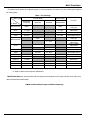
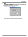
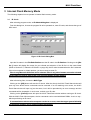
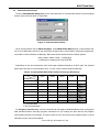
M16C Flash Start
User’s manual
MITSUBISHI ELECTRIC SEMICONDUCTOR SYSTEMS CORPORATION
Z1-MSA0806.E Rev.C
Windows 95 and Windows 98 are registered trademarks of Microsoft Corporation, US.
PC/AT is a registered trademark of IBM Corporation, US.
Revisions
Rev.A Published Sep.1999
Rev.B Published Dec.1999
Rev.C Published Jan.2000
Publisher Notes
(1) Copyright. All rights reserved. No part of this document may be reproduced without the express written
permission of MITSUBISHI ELECTRIC SEMICONDUCTOR SYSTEMS CORPORATION.
(2) The information in this document is subject to change without notice and does not represent a commitment
on the part of MITSUBISHI ELECTRIC SEMICONDUCTOR SYSTEMS CORPORATION.
(3) Should you notice anything incorrect, strange or missing in this document, contact MITSUBISHI ELECTRIC
SEMICONDUCTOR SYSTEMS CORPORATION.
(4) MITSUBISHI ELECTRIC SEMICONDUCTOR SYSTEMS CORPORATION shall assume no responsibility
whatsoever for troubles arising from the use of this product, regardless of item (3) above.
For inquiries
MITSUBISHI ELECTRIC SEMICONDUCTOR SYSTEMS CORPORATION
ENGINEERING SECTION E
ENGINEERING DEPARTMENT A
OSAKA SEMICONDUCTOR APPLICATION CENTER
FAX: (06) 6338-5193
E-mail: [email protected]
- TABLE OF CONTENTS 1 OUTLINE...............................................................................................1
2 STARTUP..............................................................................................3
3 INTERNAL FLASH MEMORY MODE..................................................4
3.1 ID Check ............................................................................................................... 4
3.2 Communications Setup....................................................................................... 5
3.3 Device Command................................................................................................. 6
•
Load (ID) ....................................................................................................... 7
•
Blank ............................................................................................................. 7
•
Read.............................................................................................................. 7
•
Status ............................................................................................................ 7
•
E.P.R ............................................................................................................. 8
•
B.P.R ............................................................................................................. 8
•
Program ........................................................................................................ 8
•
Erase............................................................................................................. 8
•
Setting ........................................................................................................... 8
•
Download ...................................................................................................... 8
•
Version .......................................................................................................... 8
•
Exit ................................................................................................................ 8
4 M16C/80 BOOT LOADER MODE........................................................9
4.1 Selecting a File .................................................................................................... 9
4.2 Communications Setup....................................................................................... 9
4.3 Device Command............................................................................................... 10
•
Load ............................................................................................................ 11
•
Blank (Note1) .............................................................................................. 11
•
Read (Note1)............................................................................................... 11
•
Status (Note1) ............................................................................................. 11
•
E.P.R (Note1) .............................................................................................. 11
•
B.P.R (Note1) .............................................................................................. 11
•
Program (Note1).......................................................................................... 11
•
Erase (Note1) .............................................................................................. 11
•
Setting ......................................................................................................... 11
•
Download .................................................................................................... 12
•
Version ........................................................................................................ 12
•
Exit .............................................................................................................. 12
5 APPENDIX ......................................................................................... 13
5.1 Memory Map....................................................................................................... 13
5.1.1 M30624FGA............................................................................................. 13
5.1.2 M30800FC ............................................................................................... 13
5.1.3 M30220FC ............................................................................................... 14
5.1.4 M30201F6 ................................................................................................ 14
5.1.5 M30802SGP ............................................................................................ 15
5.2 Standard serial I/O Mode ................................................................................... 16
5.2.1 M30800FCFP........................................................................................... 16
5.2.2 M30624FGAFP ........................................................................................ 17
5.2.3 M30220FC ............................................................................................... 18
5.2.4 M30220FC ............................................................................................... 19
5.3 About the ID Check............................................................................................ 20
5.4 Messages ........................................................................................................... 22
5.5 Example of Target Board Circuit ...................................................................... 23
5.5.1 Using High-speed Serial Cable ................................................................ 23
5.5.2 Using RS-232C Cable .............................................................................. 24
M16C Flash Start
1 Outline
M16C Flash Start (FlashSta.exe) is the software to operate on M16C microcomputers that contain internal
flash memory or those which have external M16C/80 ROM from an Windows version personal computer
(PC/AT). It has two modes of operation:
• Internal Flash Memory Mode
In this mode, the software operates on an M16C microcomputer that contains internal flash memory to
program or erase its internal flash memory.
• M16C/80 Boot Loader Mode
It allows you to download into the internal RAM of a microcomputer which comes with external
M16C/80 ROM, as well as program and erase the external flash memory (limited to only
M5M29T160BVP) mounted on the target system.
If you want to operate on external flash memory other than M5M29T160BVP, please prepare a
control program suitable for the flash memory you are using and transfer it into the internal
RAM of the microcomputer using the download function.
The following shows the operating environment for M16C Flash Start.
(1) IBM PC/AT-compatible computer running Windows 95 or later
(2) 1 serial port
M16C Flash Start requires an RS-232C serial communications cable and a voltage converter circuit that
can convert voltage to the cable's output level. (Refer to Section 5.5, "Example of Target Board Circuit" on
page 23.)
1
M16C Flash Start
The table below shows the supported types of microcomputers and how to set the related pins required
for writing data.
Table 1. Pin Settings
Internal Flash
MCU Type
Boot Loader
Function
M16C/62A
M16C/80
M16C/22
M16C/20
M30802SGP
BUSY(RTS1)
Open
-
-
Open
CLK1
“L” input
-
-
“L” input
RxD1
PC TxD
-
-
PC TxD
TxD1
PC RxD
-
-
PC RxD
-
Open
-
-
-
-
“L” input
-
-
“L” input
-
-
-
-
Vcc input
-
Serial data output
Operation monitoring pin
Switch to M16C
Flash Start
Switch to M16C
Flash Start
Mode entry
RxD0
-
PC TxD
PC TxD
-
Serial data input
TxD0
-
PC RxD
PC RxD
-
Serial data output
CNVss
Vcc input
Vpp input (*2)
Vpp input (*2)
“L” input
Mode entry
CE(*1)
Vcc input
-
-
-
Mode entry
EPM(*1)
“L” input
Reset input
Reset input
Reset input
Mode entry
RESET
Reset input
Reset input
Vcc
Vcc
Vcc
Vcc
Vcc
Power input
Vss
GND
GND
GND
GND
GND
Pin Name
BUSY(RTS0)
CLK0
Operation monitoring pin
Switch to M16C
Flash Start
Serial data input
*1: Refer to "5.2 Standard serial I/O Mode" on page 16 for pin assign.
*2: Refer to flash microcomputer datasheets.
M16C Flash Start can communicate with the target microcomputer in the range of main clock input oscillation frequencies shown below.
2 MHz to the maximum input oscillation frequency
2
M16C Flash Start
2 Startup
Execute M16C Flash Start (FlashSta.exe), and the environment setup screen shown below will appear.
Use this screen to choose program mode and serial port (COM1-4).
After selecting the above, go to each program mode.
Figure 1. Environment Setup Screen
When select "OK" button, it will take a few seconds untill next screen appears.
3
M16C Flash Start
3 Internal Flash Memory Mode
The following explains how to operate in internal flash memory mode.
3.1
ID Check
After selecting program mode, an ID Check dialog box is displayed.
From this dialog box, choose the program file to be operated on, enter ID code, and choose the type of
MCU used.
Figure 2. ID Check Dialog Box
Input the file name in the File Path field box and the ID code in the ID field box. Clicking on the [Refer…] button will display file names for your referral and selection. If the ID file is in the same folder
(Refer to Section 5.3, "About the ID Check" on page 20), the ID code is loaded when the file is selected.
If the microcomputer is a blank product, you do not need to enter ID.
Files in only Motorola S2 format can be selected. Files in any other formats cannot be selected.
The ID code you need to enter is the code currently written in flash memory.
After referencing files, choose the MCU Type.
Clicking on the [OK] button will start the ID check. After the check, the M16C Flash Start window will
open up, from where device commands can be executed. If an ID matching error occurs, the M16C
Flash Start window will open up just the same, but it will be preceded by an error message and the
commands will be inoperable. In such case, recheck your ID code.
Clicking on the [Cancel] button will open the M16C Flash Start window without running an ID check.
With the M16C Flash Microcomputer, device commands can be used with blank ROMs - that is to say without performing an ID check.
If communication with the microcomputer results in an error, reset the target system following
the messages and then set up communication back again.
4
M16C Flash Start
3.2
Communications Setup
From the Set baudrate dialog box, set the rate with which to communicate with the microcomputer
and the time interval at which to send data.
Figure 3. Communications Setup
Set a communication rate for Baud rate (bps). At the M16C Flash Start startup, communication status is set at 9600 bps. After that, the previously set baud rate is used. Before exiting the programmer,
return MCU communications to 9600 bps. Baud rate can be selected from the below speeds.
9600, 19200, 38400, 57600, *115200 (bps)
*115200 bps is supported for only M16C/80.
Depending on the microcomputer's main clock input oscillation frequency or MCU type, the selected
baud rate may result in communication error. In such a case, choose another baud rate.
Table 2. Communicable Baud Rates at Each Frequency (Reference)
Baud rate
(bps)
Xin(MHz)
9600
19200
38400
57600
115200
20
O
O
O
O
O
16
O
O
O
O
10
O
O
X
O
8
O
O
O
O
6
O
O
O
X
4
O
O
X
X
3
O
O
O
X
2
O
X
X
X
O: Communicable
X: Not communicable
For Program_intervals (ms), set a time interval from one page of data transferred to the next page of
data transferred when executing program commands. As you change the time interval, the program
commands execution time changes. The time interval is set to 40 ms when the program starts. It can be
selected from the values listed below.
5 ms to 50 ms; at intervals of 5 ms
5
M16C Flash Start
Depending on the microcomputer's operating frequency or MCU type, the time in which data is written
to flash memory varies. If a communication error occurs when executing program commands, increase
the time interval.
3.3
Device Command
The Device command dialog box is for executing device commands.
Figure 4. Device Command Dialog Box
If the flash ROM is blank, the device commands can be used even without running an ID check. With
written ROMs, until the ID check is run and completed, only the [Load (ID)], [Status], [Setting] and
[Version] commands can be used.
When the [Program] and other commands are selected, the Input Address dialog box opens up.
Enter the address range to be operated on by the command. The default address input values are the
upper-limit and lower-limit addresses in the file that was specified during ID check. (When no file is selected, the start and end addresses of M16C/62A flash memory are assumed.)
Input an address within the setting range. (Refer to Section 5.1, "Memory Map" on page 13.)
Figure 5. Input Address Dialog Box
6
M16C Flash Start
•
Load (ID)
Refer to Section 3.1, "ID Check" on page 4.
•
Blank
Checks internal flash memory for blank.
•
Read
Compares the program file specified for Load (ID) with the content written in flash memory.
•
Status
Displays the status of the flash memory.
Figure 6. Status Display Screen
The table below lists the content of each item.
Table 3. Contents of Status
Item
1
Write state machine
status
2
ID check
3
Erase
4
Program
After block
5
6
Check sum
7
Data receive timeout
Content of Processing
Shows operating status of flash memory.
[Ready]
: Program/erase ready
[Busy]
: Program/erase in progress
Shows ID check status of flash memory.
[Not Yet] : Not verified
[Not match] : Verification mismatch
[Match]
: Verified
Shows erase status of flash memory.
[Error] : Terminated in error
[Right] : Terminated normally
Shows programming status of flash memory.
[Error] : Terminated in error
[Right] : Terminated normally
Shows excessive write status when writing pages.
[Error] : Excessively written
[Right] : No excessive write
Shows boot program transfer result.
[Match]
: Checksum matched
[Not Match] : Checksum mismatched
Shows time-out occurrence status when receiving data.
[Time Out] : Time-out occurred when receiving
[Right]
: Received data normally
7
M16C Flash Start
•
E.P.R
Sequentially executes erase, program, and read commands.
•
B.P.R
Sequentially executes blank, program, and read commands.
•
Program
Writes the program file specified for Load (ID) into flash memory.
•
Erase
Unlocks each block of flash memory and then erases the entire area of flash memory.
•
Setting
Refer to Section 3.2, "Communications Setup" on page 5.
•
Download
Upgrades the control program version. The updating control program specified for Load (ID) is
downloaded into the internal RAM of the microcomputer. When the download is completed, the program transferred into the internal RAM starts operating.
•
Version
Outputs version information on the microcomputer's control program.
Figure 7. Version Information
•
Exit
Changes the communication rate to 9600 bps before quitting M16C Flash Start.
8
M16C Flash Start
4 M16C/80 Boot Loader Mode
This section explains how to use M16C/80 boot loader.
4.1
Selecting a File
After selecting program mode, a Program/Download File Select dialog box is displayed. Enter the
file name to be downloaded into the internal RAM or with which to program external flash memory.
Figure 8. Selecting a File
Input the file name in the File Path field box. Clicking on the [Refer…] button will display file names
for your referral and selection. Files in only Motorola S2 format can be selected. Files in any other
formats cannot be selected.
Click on [OK] button, and a device command dialog box will appear after completing file selection.
When you click on [Cancel] button, a device command dialog box is displayed after canceling file selection.
If communication with the microcomputer results in an error, reset the target system following
the messages and then set up communication back again.
4.2
Communications Setup
Refer to Section 3.2, "Communications Setup" on page 5.
9
M16C Flash Start
4.3
Device Command
From the Device command dialog box, execute device commands to download files into the internal
RAM, program external flash memory, etc.
Figure 9. Device Command Dialog Box
When the [Program] and other commands are selected, the Input Address dialog box opens up.
Enter the address range to be operated on by the command. The default address input values are the
upper-limit and lower-limit addresses in the file that was specified during ID check. (When no file is selected, the start and end addresses of M16C/62 flash memory are assumed.)
Enter addresses within the range in which external flash memory is located.
(Refer to Section 5.1.5, " M30802SGP" on page 15.)
Figure 10. Input Address Dialog Box
10
M16C Flash Start
•
Load
Refer to Section 4.1, "Selecting a File" on page 9.
•
Blank (Note1)
Checks external flash memory for blank.
•
Read (Note1)
Compares the program file specified for Load (ID) with the content written in external flash memory.
•
Status (Note1)
Displays the status of the external flash memory(the M5M29T160BVP). (Refer to Section 3.3,
"Status" on page 6.)
•
E.P.R (Note1)
Sequentially executes erase, program, and read commands for external flash memory.
•
B.P.R (Note1)
Sequentially executes blank, program, and read commands for external flash memory.
•
Program (Note1)
Writes the program file specified for Load (ID) into flash memory.
•
Erase (Note1)
Erases the entire area of external flash memory. However, blocks in locked state whose lock bit =
0 are not erased.
•
Setting
Refer to Section 3.2, "Communications Setup" on page 5.
(Note1) Please do not use this command except when connect specified external flash memory.
11
M16C Flash Start
•
Download
Transfers the file selected in Section 4.1, "Selecting a File," into the internal RAM of the microcomputer. When the download is completed, the program transferred into the internal RAM starts operating.
When creating a downloading program, be sure to set a version number (eight characters) at the
beginning of the program. Also, set address 000600h for the start address of the program, and make
sure the program size is within the downloadable area (000600h to 0029FFh).
[Example of downloading program]
; **********************************************************************
;
M16C/80 Flash Micon Test Program.
*
;
CPU
: M16C/80 (Xin=20.0MHZ) *
;
FUNCTION
: Port2 Rotate Output Test. *
;
CODED BY
: (Mr.Sawa)1999-05-11
*
; **********************************************************************
;------ Include Defined. ----------------------------------------------.LIST
OFF
.INCLUDE SFR80.INC
.LIST
ON
;------ Symbol Defined. -----------------------------------------------VSTACK . EQU
VRAM
. EQU
VPRO
. EQU
0002B00H; Stack-Point (ISP)
0000400H
; Internal RAM Area (0000400H - 00005FFH)
0000600H
; Download Program Area (0000600H– 00029FFH)
. SECTION
. ORG
VRAM
RAMDATA, DATA
. SECTION
. ORG
VPRO
PROGRAM, CODE
RESET:
. byte
"VER.0.05"
; Set Firmware VersionNO.
mov.b
mov.b
#0ffh,
#001h,
mov.w
sbjnz.w
#0FFFFh, R0
#1,R0,?-
; Wait
rot.b
jmp
#1,
LOOP
; Rotate P2
; Loop
PD2
P2
LOOP:
?:
P2
.END
•
Version
Outputs version information on the microcomputer's control program.
•
Exit
Changes the communication rate to 9600 bps before quitting M16C Flash Start.
12
M16C Flash Start
5 Appendix
5.1
Memory Map
5.1.1
M30624FGA
0C_0000h
Block 6: 64 Kbytes
0D_0000h
Block 5: 64 Kbytes
0E_0000h
Block 4: 64 Kbytes
0F_0000h
Block 3: 32 Kbytes
0F_8000h
Block 2: 8 Kbytes
0F_A000h
Block 1: 8 Kbytes
0F_C000h
Block 0: 16 Kbytes
0F_FFFFh
5.1.2
M30800FC
FE_0000h
Block 4: 64 Kbytes
FF_0000h
Block 3: 32 Kbytes
FF_8000h
Block 2: 8 Kbytes
FF_A000h
Block 1: 8 Kbytes
FF_C000h
Block 0: 16 Kbytes
FF_FFFFh
13
M16C Flash Start
5.1.3
5.1.4
M30220FC
0E_0000h
Block 1: 32 Kbytes
0E_8000h
Block 2: 32 Kbytes
0F_0000h
Block 3: 32 Kbytes
0f_8000h
Block 4: 32 Kbytes
M30201F6
0F_0000h
48 Kbytes
0F_FFFFh
14
M16C Flash Start
5.1.5
M30802SGP
The diagram below shows the area that can be downloaded into M16C/80 flash microcomputers using
this program.
000000h
SFR area
0003FFh
000400h
0005FFh
000600h
Internal RAM
area
0029FFh
002A00h
Downloadable area
(9K bytes)
002BFFh
002C00h
007FFFh
008000h
Internal reserved area
External area
(*)
External flash memory
connectable area
FFFFFFh
(*) For details about memory mapping, refer to M16C/80 datasheets.
.
15
M16C Flash Start
5.2
Standard serial I/O Mode
5.2.1
M30800FCFP
81
82
83
84
85
86
87
88
P0 7 /D 7
P0 6 /D 6
P0 5 /D 5
P0 4 /D 4
P0 3 /D 3
P0 2 /D 2
P0 1 /D 1
89
90
91
92
P0 0 /D 0
P1 07 / AN 7 / KI3
P1 06 / AN 6 / KI2
P1 05 / AN 5 / KI1
93
94
95
96
97
8
80 79 7 8 7 7 76 75 74 73 72 71 7 0 6 9 6 8 6 7 66 65 6 4 63 62 61 6 0 5 9 58 5 7 56 55 54 53 52 51
3
BYTE
CN Vss
P8 7 /X CIN
P 8 6 / X CO U T
R ES ET
98
P9 4 /D A 1 /TB4 IN /C TS 4 /RT S 4 /SS 4
P9 3 /D A 0 /TB 3 IN /C TS 3 / RT S 3 /SS 3
P9 2 /TB2 IN /T X D 3 / SDA 3 / SRxD 3
P9 1 /T B1IN /R X D 3 /SC L 3 /STxD 3
P9 0 /T B0 IN/ CL K 3
2
P7 6 /TA3 O U T
P7 5 /T A2I N/ W
P7 4 /T A2O U T/ W
P7 3 /C TS 2 /R TS 2 / TA 1 IN /V
P7 2 /C LK 2 / TA1 O UT /V
P7 1 /R xD 2 /SC L 2 /TA0 IN /TB 5 IN
P70 / T X D 2 /SD A 2 /TA 0 O U T
9 10 1 1 1 2 1 3 1 4 15 16 1 7 1 8 19 20 21 22 23 24 2 5 2 6 2 7 28 29 30
P 8 0 /TA4 O U T/U
P7 7/TA 3 IN
7
P 84 /IN T 2
P83 / IN T1
P 82 /IN T 0
P8 1 /TA4 IN/U
6
V SS
X IN
VCC
P8 5 /N M I
5
XOU T
4
Co nnec t
circu it
os cilla tio n
R ESET
P9 6/ ANEX 1/T X D 4 / SDA 4 / SRxD 4
P9 5 /AN EX0/ CL K 4
1
C N Vss
Vcc
P104 /AN 4/ KI0
P10 3 /AN 3
P10 2 /AN 2
P10 1 /AN 1
AV SS
CE
Vss
Vss >> Vcc
99
R ESET
P10 0 /AN 0
VRE F
AVc c
EPM
Va lu e
Vcc
100
C NVss
P9 7 /A D TRG / RX D 4 /SC L 4 /STxD 4
M o de se tt ing
S ign a l
M 16C /8 0(10 0-p in ) Gr ou p
F las h M em o ry V ers io n
(100 P 6S )
50
49
P4 4 /C S3/ A20 (M A12)
P4 5 /C S2/A 21
P5 0 /W R L /WR/C AS L
P4 6 /C S1/A 22
P4 7 /C S0/A 23
48
47
P5 1 /W R H /BH E/CASH
P5 2 /R D/DW
P5 3 /BC LK/ ALE/CLK OU T
P5 4 /H LD A/AL E
P5 5 /H OLD
P5 6 /AL E/R AS
P5 7 /R DY
P6 0 /C TS 0/R TS 0
P6 1 /CLK 0
P6 2 /R xD 0
P6 3 /TXD 0
P6 4 /C TS 1 /R TS 1/CT S 0 /C LKS 1
P6 5 /CLK 1
P6 6 /RxD 1
P6 7 /T XD 1
46
45
44
43
42
41
40
39
38
37
36
35
34
33
32
31
CE
EPM
BUSY
RxD
Vss
Vcc
SC L K
TxD
Figure 11. Pin Connections for Serial I/O Mode (1)
16
P1 0/D 8
P1 1/D 9
P1 2/D 10
P1 3/D 11
P1 4/D 12
P1 5/D 13 /IN T3
P1 6/D 14 /IN T4
P1 7/D 15 /IN T5
P2 0/A 0 (/D 0 )
P2 1/A 1 (/D 1 )
P2 2/A 2 (/D 2 )
P2 3/A 3 (/D 3 )
P2 4/A 4 (/D 4 )
P2 5/A 5 (/D 5 )
P2 6/A 6 (/D 6 )
P2 7/A 7 (/D 7 )
Vss
P3 0/A 8 (M A0 )(/D 8 )
Vcc
P3 1/A 9 (M A1 )(/D 9 )
P3 2/A 10 (M A2 )(/D 10 )
P3 3/A 11 (M A3 )(/D 11 )
P3 4/A 12 (M A4 )(/D 12 )
P3 5/A 13 (M A5 )(/D 13 )
P3 6/A 14 (M A6 )(/D 14 )
P3 7/A 15 (M A7 )(/D 15 )
P4 0/A 16 (M A8 )
P4 1/A 17 (M A9 )
P4 2/A 18 (M A1 0)
P4 3/A 19 (M A1 1)
M16C Flash Start
5.2.2
M30624FGAFP
CE
P0 7/D 7
P0 6/D6
P0 5/D5
P0 4/D 4
P0 3/D3
P0 2/D 2
P0 1/D 1
P0 0/D0
P107/AN7/KI3
P106/AN6/KI2
P105/AN5/KI1
P104/AN4/ KI0
P10 3/AN 3
P10 2/AN 2
P10 1/AN 1
AVSS
P10 0/AN 0
VRE F
AVcc
P9 7/ADTRG/S IN4
Mode setup method
Value
Signal
CNVss
Vcc
EPM
Vss
RESET
Vss to Vcc
Vcc
81
82
83
84
85
86
87
88
89
90
91
92
93
94
95
96
97
2 3
4 5
6 7 8 9 10 11 12 13 14 15 16 17 18 19 20 21 22 23 24 25 26 27 28 29 30
Connect
oscillator
circuit.
80 79 78 77 76 75 74 73 72 71 70 69 68 67 66 65 64 63 62 61 60 59 58 57 56 55 54 53 52 51
1
RESET
98
99
100
CNVss
P96/ANEX1/SOUT4
P9 5/ANEX0/CLK4
P94/DA1/TB4 IN
P93/DA0/TB3 IN
P92/TB2 IN/SOUT3
P91/TB1 IN/SIN3
P90/TB0 IN/CLK3
BYTE
CNVss
P8 7/XCIN
P8 6/X COUT
RESET
X OUT
VSS
XIN
VCC
P8 5/NMI
P84/INT2
P83/INT1
P82/INT0
P8 1/TA4 IN/U
P8 0/TA4OUT/U
P7 7/TA3IN
P76/TA3 OUT
P7 5/TA2IN/W
P74/TA2OUT/W
P7 3/CTS 2/RTS2/TA1 IN /V
P7 2/CLK2/TA1 OUT /V
P71/RxD 2/SCL/TA0IN /TB5 IN
P70/TXD 2/SDA/TA0 OUT
M1 6C/6 2A fla sh
me mor y ve rsi o n
(100 P6S)
50
49
48
47
46
45
44
43
42
41
40
39
38
37
36
35
34
33
32
31
P4 4/CS0
P4 5/CS1
P4 6/CS2
P4 7/CS3
P50/WRL/WR
P51/WRH/BHE
P52/RD
P53/BCLK
P5 4/HLDA
P5 5/HOLD
P56/ALE
P5 7/RDY/CLKOUT
P60/CTS0/RTS0
P6 1/CLK0
P6 2/RxD0
P6 3/TXD 0
P6 4/CTS1/RTS1/CTS0/CLKS1
P6 5/CLK1
P66/RxD1
P67/TXD 1
CE
EPM
BUSY
RxD
Vss
Vcc
SCLK
TxD
Figure 12. Pin Connections for Serial I/O Mode (2)
17
P10/D 8
P11/D 9
P12/D 10
P13/D 11
P14/D 12
P15/D 13/INT3
P16/D 14/INT4
P17/D 15/INT5
P2 0/A0(/D 0/-)
P2 1/A1(/D 1/D0)
P2 2/A2(/D 2/D1)
P2 3/A3(/D 3/D2)
P2 4/A4(/D 4/D3)
P2 5/A5(/D 5/D4)
P26/A6(/D6/D 5)
P27/A7(/D7/D 6)
Vss
P30/A8(/-/D7)
Vcc
P31/A9
P3 2/A10
P3 3/A11
P3 4/A12
P3 5/A13
P3 6/A14
P3 7/A15
P4 0/A16
P4 1/A17
P4 2/A18
P4 3/A19
M16C Flash Start
M30220FC
74
73
75
76
77
79
78
80
81
83
82
84
85
86
88
87
89
90
91
93
92
94
95
97
96
98
100
99
102
101
103
104
106
105
110
72
71
111
70
112
113
69
114
67
66
109
68
115
116
117
65
118
63
62
64
119
120
121
61
122
59
58
60
123
57
124
125
M30220 flash memory version
(144P6Q-A, 144PFB-A)
126
127
128
129
56
55
54
53
52
130
51
131
50
49
132
133
48
134
47
135
46
45
136
137
44
138
43
139
42
41
140
141
40
142
39
143
38
37
TxD
CE
No te1
RESET
No te2
VPP
Mode setup method
Signal
CNVss
RESET
CE
Value
4.5V to 5.5V
Vss
Vcc
Vcc
Note 1: Connect oscillator ci rcui t.
Note 2: Connect to V CC when V CC = 4.5V to 5.5 V.
Connect to Vpp (=4.5V to 5.5 V) when V CC = 2.7V to 4.5 V.
Figure 13. Pin Connections for Serial I/O Mode (3)
18
BUSY
RxD
SCLK
36
35
34
32
33
31
30
29
27
28
26
25
23
24
22
21
20
18
19
17
16
14
15
13
12
11
9
10
8
7
5
6
4
3
P1 5/KI5
P1 6/KI6
P1 7/KI7
P2 0/KI8
P2 1/KI9
P2 2/KI1 0
P2 3/KI1 1
P2 4/KI1 2
P2 5/KI1 3
P2 6/KI1 4
P2 7/KI1 5
P3 0/KI1 6
P3 1/KI1 7
P3 2/KI1 8
P3 3/KI1 9
P3 4
P3 5
P4 0/TA0OUT
P4 1/TA0IN
P4 2/TA1OUT
P4 3/TA1IN
P4 4/TA2OUT
P4 5/TA2IN
P4 6/TA3OUT/INT4
P4 7/TA3IN /INT4
P5 0/TB0IN
P5 1/TB1IN
P5 2/TB2IN
P5 3/TB3IN
P5 4/TB4IN
P5 5/TB5IN
P5 6/INT3
P5 7/CK OU T
P60/CTS0/RTS 0
P61/CLK0
P62/RxD0
P9 6/AN6
P9 5/AN5
P94/AN4
P9 3/AN3
P9 2/AN2
P9 1/AN1
P9 0/AN0
P8 7/TA7 IN
P86 /TA7OUT
P85/TA6IN
P84 /TA6OUT
P8 3/TA5 IN
P82 /TA5OUT
P8 1 /TA4IN/INT 5
P80/TA4OUT/INT 5
CNV SS
X CIN
X COUT
RESET
XOUT
V SS
X IN
VCC
P7 7/NMI
P76/INT 2
P75/INT 1
P74/INT 0
P7 3/CTS2 /RTS2
P72/CLK2
P71/RXD2/SCL
P70/TXD2/SDA
P67/TxD1
P66/RxD1
P65/CLK1
P64 /CTS 1/RTS1/CTS 0/CLKS1
P63/TxD0
2
144
1
SEG 18/P102
SEG 17/P101
SEG 16/P10 0
SEG1 5
SEG14
SEG13
SEG12
SEG1 1
SEG10
SEG 9
SEG8
SEG 7
SEG 6
SEG 5
SEG 4
SEG 3
SEG 2
SEG 1
SEG 0
COM3
COM2
COM1
COM0
C2
C1
VL 3
VL 2
VL1
Vss
P13 2/DA 2
P13 1/DA 1
AV SS
P130 /ADTRG /DA0
VREF
AVCC
P97/AN7
107
108
SEG 19/P10 3
SEG 20/P10 4
SEG 21/P10 5
SEG 22/P10 6
SEG 23/P10 7
SEG 24/P11 0
SEG 25/P11 1
SEG 26/P11 2
SEG 27/P11 3
SEG 28/P11 4
SEG 29/P11 5
SEG 30/P11 6
SEG 31/P11 7
SEG 32/P12 0
SEG 33/P12 1
V SS
SEG 34/P1
2V2CC
SEG 35/P12 3
SEG 36/P12 4
SEG 37/P12 5
SEG 38/P12 6
SEG 39/P12 7
SEG 40/P00
SEG 41/P01
SEG 42/P02
SEG 43/P03
SEG 44/P04
SEG 45/P05
SEG 46/P06
SEG 47/P07
P10/KI0
P11/KI1
P12/KI2
P1 3/KI3
P14/KI4
5.2.3
VCC
VSS
M16C Flash Start
M30201F6
Mode setup method
P45/ TX2INOUT
P6 6/AN6
P6 1/AN1
P6 2/AN2
P6 3/AN3
P6 4/AN4
P6 5/AN5
P6 0/AN0
AV SS
30
29
P4 2/RXD1
P4 1/TA0OUT
P4 0/TA0IN/TXD 1
15
16
P4 4/INT1/TX1INOUT
P4 3/INT0/TX0INOUT
9
10
11
12
13
14
26
27
28
VC C
VSS
XIN
VCC
M30201F6FP
M30201F6TFP
P15 (LED 5)
P14 (LED 4)
VSS
6
7
8
39
38
37
36
35
34
33
32
31
P3 0
P17 (LED 7)
P16 (LED 6)
N.C.
XOUT
42
41
40
P3 3
P3 2
P3 1
RESET
P7 1/TB1IN/X CIN
P70 /TB0IN/XCOUT
RESET
1
2
3
4
5
20
21
22
23
24
25
CNVSS
P5 1/RXD 0/AN 51
P5 0/TXD 0/ AN 50
CNVSS
N.C.
P3 5
P3 4
TXD
17
18
19
R XD
49
48
47
46
45
44
43
N.C.
AV CC
VREF
VSS
VCC
BUSY
VC C
SCLK
VPPH
VSS
56
55
54
53
52
51
50
RESET
P5 2/CLK0/AN52
Value
CNVSS
P5 3/CLKS/AN 53
P5 4/CKOUT/AN54
Signal
Connect oscillator
circuit.
5.2.4
Figure 13. Pin Connections for Serial I/O Mode (3)
19
P6 7/AN7
N.C.
P0 0/KI0
P0 1/KI1
P0 2/KI2
P0 3/KI3
P0 4/KI4
P0 5/KI5
P0 6/KI6
P0 7/KI7
P10 (LED 0)
P11 (LED 1)
P12 (LED 2)
P13 (LED 3)
M16C Flash Start
5.3
About the ID Check
The ID check compares the ID code stored in the flash ROM against the ID code sent via serial com-
munications. Unless the two ID codes match, certain commands are disabled. The table below lists the
areas in which ID code is stored.
Table 4. ID Address
MCU
Type
M16C/62A
M16C/20
M16C/80
ID Address
ROM code protect information
0FFFDFh,0FFFE3h,0FFFEBh,0FFFEFh,0FFFF3h,0FFFF7h,
0FFFFBh
0FFFFDFh,0FFFFE3h,0FFFFEBh,0FFFFEFh,0FFFFF3h,
0FFFFF7h,0FFFFFBh
0FFFFFh
0FFFFFFh
S2140FFFB0E8C5EEC5F4C5FAC500C606C60CC612C619
S2140FFFC018C61EC624C62AC630C636C63CC642C685
S2100FFFD048C64EC654C65AC660C665C664
S2140FFFDCCDC60F0050C70F00D8C70F00CFC80F00E5
S2140FFFEC13CA0F005BC80F004DCB0F004ECB0F0084
S2080FFFFC18CD0F00F9
S804000000FB
Figure 14. Motorola S2 File – ID Address (M16C/62A)
By creating an ID file with an ID code and ROM code protect information (ROM protect during parallel
writing), the ID code is automatically loaded when your work file is selected in the ID Check dialog box
(Refer to Section 3.1, "ID Check" on page 4).
The ID file can be created with the -ID option of LMC30 (LMC308). The ROM code protect can be set
with the -protect option.
LMC30 (LMC308) is included in Mitsubishi's NC30 (NC308) compiler and AS30 (AS308) assembler
for M16C and are supported in following versions.
LMC30
; V.3.10.00
LMC308
; V.1.00.01
It is explained here following how to set IDs, create files and protect data with LMC30.
(1) ID Setting
• The ID code is set with the -ID option. Only capital letters "ID" are accepted.
• Immediately after inputting "-ID", input an ID code as # plus a hexadecimal number or in singlebyte alphabetic characters.
• "H" is not needed to indicate the hexadecimal number.
• An error occurs if the ID code exceeds 56 bits.
20
M16C Flash Start
• To set an ID code as a hexadecimal number, add # after inputting "-ID". Numbered codes can be
up to 14 digits long.
• To set an ID code in single-byte alphabet input the text string after inputting "-ID". Lettered codes
can be up to seven characters long and must be single-byte ASCII code (30h - 39h, 41h - 5Ah and
61h – 7Ah).
Example: -ID#1234
The ID is 12340000000000. It is stored as "12h" in address FFFDFh, "34h" in address FFFE3h
and "00h" in addresses FFFEBh, FFFEFh, FFFF3h, FFFF7h and FFFFBh.
Example: -IDCODE
The ID is 434F4445000000. It is stored as "43h" in address FFFDFh, "4Fh" in address FFFE3h,
"44h" in address FFFEBh, "45h" in address FFFEFh and "00h" in addresses FFFF3h, FFFF7h
and FFFFBh.
(2) ID File Output
When the -ID option is input, LMC30 creates a file containing the ID code and ROM code protect
information (address FFFFFh), and names it with the HEX file (Motorola S2 format) ".id" extension.
Example: LMC30 -ID#1234 samp
A file with the below contents will be created under the name “samp.id”.
-ID1234
FFFDF
FFFE3
FFFEB
FFFEF
FFFF3
FFFF7
FFFFB
FFFFF
:
:
:
:
:
:
:
:
12
34
00
00
00
00
00
FF
Figure 15. ID File Contents
*The ID code input at LMC30 startup is output on the first line, while all of the ID addresses and
the code values set for each are output on the following lines.
*If the -protect option has been input, "-protect" is output on the first line.
(3) Protect Option
• The protect function is set using the -protect option. Only small case letters are accepted.
• At LMC30 startup, "30" is set for address FFFFFh if the -protect option is used. Otherwise, "FFh" is
set for address FFFFFh.
If LMC30 cannot create an ID file, create one like that in Figure 15.
21
M16C Flash Start
5.4
Messages
The below messages are displayed when device commands are executed or errors occur.
Table 5. Messages
Type
No.
1
Can not communicate.
Description
Communications were not established with
the target MCU.
Remedial action
Check the following.
* That power to the target MCU is ON.
* That the communications cable is correctly
connected.
* Whether SCLK and CNVss are correctly set.
2
Can not communicate to outside.
Communications with the target MCU are
not possible.
3
Timeout.
Push RESET.
The target MCU did not reply before the
communication time limit ran out.
4
Communication error.
Push RESET.
A communication error other than the above
time-out has occurred.
The error could be caused by something
other than this programmer.
5
Can not set baudrate to 9600bps.
The baud rate was not returned to 9600 bps
before exiting the programmer.
To continue using this programmer, reset the
target MCU.
6
Can not set default baudrate.
Baudrate is last baudrate.
Baud rate could not be set to 9600 when the
programmer was started up.
7
Can not set last boudrate.
Baudrate is 9600bps. Now.
At startup, the last used baud rate could not
be set. Baud rate remains the same 9600
bps for establishing communications.
8
Can not set new baudrate.
Baudrate is last baudrate now.
The programmer could not update the baud
rate.
Use a lower baud rate.
9
Can not use the Micon.
Close this program.
The target MCU did not reply during the
communication check run at startup.
See Nos. 1- 3.
10
This program is already runninig.0
11
Did not pass ID.
The ID code did not match that of the target
MCU.
12
Download Completed.
Downloading the selected file terminated
normally.
13
Download not completed.
Please retry Download.
Error occurred when downloading the selected file.
14
Erase error.
The programmer could not erase the target
MCU.
-
15
Erase OK.
The programmer has finished erasing the
target MCU.
-
16
Find not blank at address
[ADDRESS].
Blank check error. There is an area without
an FFh address.
17
Find not match at address
[ADDRESS].
Read verify error. The selected content is
different from the written content.
18
Not match ID.
The wrong ID code was input.
19
Program error.
Programming has failed.
-
20
Stop downloading.
Download operation has been suspended.
-
21
Stop programming.
Programming has been suspended.
-
22
Too higher end address (0x2A00).
The last address of the file to be downloaded
exceeds address "2A00h."
Correct the file to be downloaded.
23
Too small start address.
The start address is larger than the end
address.
Set an effective address.
24
Can not accept this file.
The selected file cannot be loaded.
The file is of the wrong format. Select a
Motorola S2 file.
25
Can not found the ID file.
The ID file was not found during the file
check.
Check whether there is an ID file in the folder
or not.
26
Do not input filename.
A file was not selected for the ID check.
Input a file name.
27
Do not match ID style.
The ID code is of the wrong style.
Input an ID code of the correct style.
Communication
Device
command
File operation
Message
Reset the target MCU as instructed in messages.
-
22
Run an ID check.
-
Execute downloading the file again.
The ROM is already written. Erase it.
Input the correct ID code.
M16C Flash Start
5.5
Example of Target Board Circuit
5.5.1
Using High-speed Serial Cable
(When using high-speed serial cable included in the MSA0806)
0.1uF
Vcc
0.1uF
10-9 Cable
Vcc
1
14
64
RxD
IBM PC/AT
96
38
GND
37
TxD
Vcc
AVs
s
P60/CTS0/
RTS0
P61/CLK0
P62/RxD 0
35
P63/TxD0
34
P64/CTS1/RTS1/CTS0/
CLK1
P65/CLK1
32
31
30
29
28
27
26
25
24
23
5k
Vcc
Vss
36
33
Connector Type
Straight (HIF3FC-10PA-2.54DSA)
Angle (HIF3FC-10PA-2.54DS)
Vss
P66/RxD 1
P67/TxD1
P70/TxD2/SDA/
TA0out
P71/RxD 2/TA0in/TB5in
P72/CLK2/RTS2/TA1out/
V
P73/CTS2/RTS2/TA1in/
*
P7
V 4/TA2out/W
P75/TA2in/*W
P76/TA3out
P77/TA3in
99
P20/A0(/D0/-)
P2 1/A1(/D1/D 0)
P2 2/A2(/D3/D 2)
P2 3/A3(/D3/D 2)
P2 4/A4(/D4/D 3)
P2 5/A5(/D5/D 4)
P2 6/A6(/D6/D 5)
P2 7/A7(/D7/D 6)
72
71
70
69
68
67
66
65
P30/A8(/-/D7)
P31/A9
P3 2/A10
P3 3/
A12
P3 4/A
11
P3 5/A13
P3 6/A14
P3 7/A15
Signal
22
Vcc
21
P81/TA4in/*U
2
20
P82/INT0
P10/D 8
3
19
Pin No
Port
1
4
p6_6
Vcc
RxD
18
5k
5
17
6
11
10
7
6
5
4
3
2
1
100
7
GND
8
9
10
p6_7
TxD
97
30pF
Vcc
10MHz
30pF
5k
0.1uF
P85/NMI
P86/Xcout
P87/Xcin
P91/TB1in/Sin3
P90/TB0in/CLK3
P92/TB2in/Sout3
P93/DA0/TB3in
P94/DA1/TB4in
P95/ANEX0/CLK4
P96/ANEX1/Sout4
P97/ADTRG/Sin4
P1 2/D 10
P1 3/
D11
P1 4/
D12
P1 5/D 13/INT3
P1 6/D 14/INT4
Xin
13
Xout
RESET
BYTE
CNVss
P1 7/D 15/INT5
P4 0/
P4 1/A
A17
16
P4 2/A18
P4 3/
A
P4 4/CS0
19
P4 5/
CS1
P4 6/
P4 7/
CS2
CS3
P50/WRL/
WR
P51/WRH/
P5 2BHE
/RD
P53/BCLK/
CLKout
P5 4/
P55/HOLD
HLDA
P5 6/
P5 7/
ALE
RDY
M30624FGAFP
JUMPER
5k
Figure 16. Example of Target Board Circuit 1
23
63
61
60
59
58
57
56
55
Vcc(5V)
DIODE
0.1uF
88
87
86
85
84
83
82
81
80
79
78
77
76
75
74
73
54
53
52
51
50
49
48
47
CON1
1
2
2pin
P100/AN0
15
9
5k
P11/D 9
98
P84/INT2
P101/AN1
P102/AN2
P103/AN3
P104/AN4/KI0
P105/AN5/KI1
P106/AN6/KI2
P107/AN7/KI3
8
Vcc
P83/INT1
95
94
93
92
91
90
89
12
Push
SW
P80/TA4out/U
62
AVc
c
AVref
P0 0/
P0D10/
P02/D
D21
P03/D 3
P04/D 4
P05/D 5
P06/D 6
P07/D 7
Pin Assignment
16
Vcc
5k
46
45
44
43
42
41
40
39
5k
M16C Flash Start
5.5.2
Using RS-232C Cable
0.1uF
VCC
D-SUB9
CONNECTOR
IBM PC/AT
GND 5
TDR 4
TxD 3
RxD 2
6
16
DSR
0.1uF
CTS
0.1uF
7
8
9
1
RS-232C
straight
0.1uF
0.1uF Extermal condensor
+5V RS-2324 Transceivers
(MAX202)
0.1uF
2
6
VC
C
C1+
1
14
Vss
Vcc
64
Vss
Vcc
3
96
4
38
AVs
s
P6 0/CTS0/
RTS0
P6 1/CLK0
0.1uF
V+
C1-
V-
C2+
0.1uF
15
14
13
7
8
GN
D
T1OU
T
C2T1IN
R1IN
R1OUT
T2OU
T2IN
T
R2IN
R2OU
37
5
36
11
35
12
34
10
33
32
9
T
5k
P7 0/TxD2/SDA/
TA0out
P7 1/RxD 2/TA0in/TB5in
P7 2/CLK2/RTS 2/TA1out/
V7 3/CTS2/RTS2/TA1in/
P
*
P7
V 4/TA2out/W
P7 5/TA2in/*W
P7 6/TA3out
P7 7/TA3in
30pF
5k
P1 0/D8
95
94
93
92
91
90
89
P8 6/Xcout
P8 7/Xcin
P9 1/TB1in/Sin3
P9 0/TB0in/CLK3
P9 2/TB2in/Sout3
P9 3/DA0/TB3in
P9 4/DA1/TB4in
P9 5/ANEX0/CLK4
P9 6/ANEX1/Sout4
P9 7/ADTRG/Sin4
Xout
RESET
BYTE
CNVss
P1 2/D10
P1 3/
D11
P1 4/
D12
P1 5/D13/INT3
P1 6/D14/INT4
P1 7/D15/INT5
P4 0/
P4 1/A
A17
16
P4 2/A18
P4 3/
A19
P4 4/CS0
P4 5/
CS1
P4 6/
P4 7/
CS2
CS3
P50/WRL/
WR
P5 1/WRH/
P5 2BHE
/RD
P5 3/BCLK/
CLKout
P5 4/
P55/HOLD
HLDA
P5 6/
P5 7/
ALE
RDY
M30624FGAFP
JUMPE
R
5k
Figure 17. Example of Target Board Circuit 2
24
63
61
60
59
58
57
56
55
Vcc(5V
)
DIODE
0.1uF
CON1
1
2
2pin
88
87
86
85
84
83
82
81
80
79
78
77
76
75
74
P100/AN0
P101/AN1
P102/AN2
P103/AN3
P104/AN4/KI0
P105/AN5/KI1
P106/AN6/KI2
P107/AN7/KI3
13
9
5k
P8 5/NMI
Xin
8
Vcc
P1 1/D9
98
P8 4/INT2
15
12
0.1uF
P3 0/A8(/-/D7)
P3 1/A9
P3 2/A10
P3 3/
A12
P3 4/A
11
P3 5/A13
P3 6/A14
P3 7/A15
P8 2/INT0
97
10MH
z
72
71
70
69
68
67
66
65
P8 1/TA4in/*U
11
10
7
6
5
4
3
2
1
100
Vcc
P2 0/A0(/D0/-)
P2 1/A1(/D1/D0)
P2 2/A2(/D3/D2)
P2 3/A3(/D3/D2)
P2 4/A4(/D4/D3)
P2 5/A5(/D5/D4)
P2 6/A6(/D6/D5)
P2 7/A7(/D7/D6)
20
P8 3/INT1
62
99
21
P8 0/TA4out/U
16
AVc
c
AVref
P0 0/
P0D10/
P0 2/D
D21
P0 3/D3
P0 4/D4
P0 5/D5
P0 6/D6
P0 7/D7
17
30pF
P6 6/RxD 1
30
29
28
27
26
25
24
23
18
5k
P6 3/TxD0
P6 4/CTS1/RTS1/CTS 0/
CLK1
P6 5/CLK1
P6 7/TxD1
19
Vcc
P6 2/RxD 0
31
22
Push
SW
Vcc
73
54
53
52
51
50
49
48
47
Vcc
5k
46
45
44
43
42
41
40
39
5k
M16C Flash Start
25
M16C Flash Start User’s manual Rev.C
Published Jan. 2000
Edited by
MITSUBISHI ELECTRIC SEMICONDUCTOR SYSTEMS CORPORATION
Published by
MITSUBISHI ELECTRIC SEMICONDUCTOR SYSTEMS CORPORATION
This book, or parts thereof, may not be reproduced in any form without permission of Mitsubishi Electric Semiconductor Systems Corporation.
©1999 MITSUBISHI ELECTRIC SEMICONDUCTOR SYSTEMS CORPORATION