1
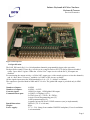
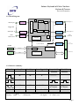
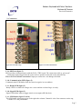
Istituto Nazionale di Fisica Nucleare
Sezione di Ferrara
Servizio Elettronico
Istituto Nazionale di Fisica Nucleare
Sez di Ferrara.
-------------------- PAX PS Board User Manual ---------------
Author:…………………………………………………………………………………Roberto Malaguti
Project by:…………………………………………………. Angelo Cotta Ramusino, Roberto Malaguti
Via Saragat 1
44100 Ferrara
http://www.fe.infn.it/servizi/elettronica/
printed in Ferrara 10 April 2008
Version 1.1
Pag.1
Istituto Nazionale di Fisica Nucleare
Sezione di Ferrara
Servizio Elettronico
Index
1.0: Specification.................................................................................................................. 4
1.1: Block Diagram.............................................................................................................. 5
1.2: Behavior summary....................................................................................................... 5
1.3: Simulations diagrams: ................................................................................................. 6
2. Connectors: ...................................................................................................................... 7
2.1.a: SPI Port (figure 5) .........................................................................................................................7
2.1.b: Communication LED (figure 5) ...................................................................................................7
2.1.c: Ready LED (figure 5) ....................................................................................................................7
2.1.d: Signal LED (figure 5) ....................................................................................................................7
2.1.e: NIM Inputs (figure 5 and 6)..........................................................................................................7
2.1.f: NIM Outputs (figure 5 and 6) .......................................................................................................8
2.1.g: Veto in (figure 6)............................................................................................................................8
2.1.h: Global OR output (figure 6) .........................................................................................................8
2.1.i: ECL Outputs (figure 6)..................................................................................................................8
2.1.j: ECL spare Outputs (figure 6) .......................................................................................................8
2.1.k: UART + JTAG port (figure 7) .....................................................................................................8
2.1.l: In-System Programming of Serial Configuration Device (figure 7)..........................................8
2.1.m: CPLD JTAG port (figure 8)........................................................................................................8
2.1.n: J1 VME connector (figure 9)........................................................................................................9
2.1.o: Push button Reset (figure 10) .......................................................................................................9
3.0: Before installation:..................................................................................................... 10
4.0: Operating instructions:.............................................................................................. 11
4.1: Presentation message coming from PAX_PS at reset:................................................................11
4.2: Choice “a”:
Parametric Setting Menu.....................................................................................12
4.3: Choice “b”: Diagnostic menu ....................................................................................................12
4.4: Choice “c”: Listen to PAX_SPI commands ............................................................................12
4.5: Choice “a+a”: Parametric Setting Menu / Set a parameter on board ..................................12
4.6: Choice “a+b”: Parametric Setting Menu / Read Rate Meters Counters ...............................13
4.7: Choice “a+c”: Parametric Setting Menu / Read and Print all parameters stored on board.
13
4.8: Choice “a+d”: Parametric Setting Menu / Store all parameters previously read from board
to Non Volatile Memory........................................................................................................................13
4.9: Choice “a+e”: Parametric Setting Menu / Read and Print all parameters present in Non
Volatile Memory
14
4.10: Choice “a+f”: Parametric Setting Menu / Configure board with parameters read from
Non Volatile Memory. ...........................................................................................................................14
5: Measurements................................................................................................................ 15
5.1 NIM & ECL signals:........................................................................................................................15
5.2 Timing:..............................................................................................................................................15
Table 2: Board “1” time measurement................................................................................................17
Table 3: Board “2” time measurement................................................................................................18
5.3: TDC time jitter evaluation: ...........................................................................................................19
6:Schematic Diagrams inside the CPLD:........................................................................ 20
6.1: The Global OR output ...................................................................................................................20
Pag.2
Istituto Nazionale di Fisica Nucleare
Sezione di Ferrara
Servizio Elettronico
6.2 The Prescaler Counter (1 of 16) .....................................................................................................20
6.3 The Rate Meter Counter (1 of 16) ..................................................................................................20
7.0: Board Schematic. ....................................................................................................... 21
7.1: The input circuit .............................................................................................................................21
7.2: The output circuit...........................................................................................................................22
7.3:The NIOS processor ........................................................................................................................22
Pag.3
Istituto Nazionale di Fisica Nucleare
Sezione di Ferrara
Servizio Elettronico
Figure 1: Board picture
1.0: Specification
The PAX_PS board (fig.1) is a 16 independent channels programmable trigger pulse prescaler.
Each prescaler counter (Count Reg.) can be set in a range from 0 to 65535 or can be software disabled
with a “Input Mask” register. When the “Global Veto” input is active all the PAX_PS outputs are
disabled.
For monitoring the output activity a “Global OR” output port (with a mask register to select the channels)
and 16 “Rate Meters Counters” readable via UART or SPI port are available.
All the signals inputs meet the NIM standard level (0 = 0V, 1= -800mV on 50ohm).
The outputs are provided both in NIM and ECL levels. The global OR output is provided only in NIM
level.
Numbers of inputs :
Numbers of outputs:
Controls signals:
Communications port:
Board Dimension:
Weight:
Power supply:
16 NIM.
16 NIM + 16 ECL.
1 NIM Veto input, 1 NIM global-OR output.
1x UART (115200bps 8–N-1),
2x JTAG ports (J7= CPLD , J6= FPGA),
1x Active Serial Programming port (J5)
1x SPI communication (J2),
1x parallel private BUS on P2 VME connector (not jet implemented).
VME 6U (233.35 x 160 mm) .
450gr.
5V (+/- 5%) 2Amp (from standard VME P2 backplane). Forced ventilation
is recommended.
Pag.4
Istituto Nazionale di Fisica Nucleare
Sezione di Ferrara
Servizio Elettronico
1.1: Block Diagram
N
NIM-input 1
Count Reg
AND
Nim to LVTTL
INPUT MASK
Trigger INs
NIM-Output 1
LVTTL to NIM
Trigger OUT
N
Count Reg
NIM-input 16
NIM
Global Veto
AND
Nim to LVTTL
Nim to LVTTL
OR
LVTTL to NIM
NIM-Output 16
LVTTL to NIM
NIM
Global OR
COUNT,,MASK
set & read
16
LVTTL to ECL
Cyclone II FPGA
SPI-BUS
SPI BUS
connector
UART
16 x
Trig ECL OUT
16 x RateMeters
Counters
SPI
NIOS processor
P2 DATA BUS
RS-232
P2 Connector
connector
ECL Connector
MAX II CLPD
AUX BUS 8bit
1.2: Behavior summary
IN 0~15
X
N pulse
Glossary:
Veto IN
“1”
Mask Reg.
X
Count Reg. 0~15
X
“0”
“0”
X
“0”
“1”
0x0000
“0”
“1”
0x0001
“0”
“1”
M = 1 To 65535
= NIM pulse.
= No signal.
Output 0~15
N / (M+1)
Global OR
N / (M+1)
X = Don’t care.
Pag.5
Istituto Nazionale di Fisica Nucleare
Sezione di Ferrara
Servizio Elettronico
1.3: Simulations diagrams:
Fig. 2: Mask Register (in simulation called “Enable”) stops the prescaler counting (last row in diagram)
and disables the trigger output.
Figure 2
Fig.3: When a new prescaler factor is set, it has effect only when the previous count is completed.
Figure 3
Fig:4: Veto input disables PAX_PS trigger outputs, the trigger count is non affected.
Figure 4
Pag.6
Istituto Nazionale di Fisica Nucleare
Sezione di Ferrara
Servizio Elettronico
2. Connectors:
Figure 5: Front Panel Top
Figure 6: Front Panel Bottom
2.1.a: SPI Port (figure 5)
SPI Port allows communication with the PAX_CTRL board. The connection cable is “pin to pin”.
Different boards plugged into the same crate are parallel connected to the same SPI bus.
This is NOT a Ethernet connection! Improper connection can damage the board.
2.1.b: Communication LED (figure 5)
Communication LED blinks when the board recognise its own address.
2.1.c: Ready LED (figure 5)
Ready LED is on when all voltages are correct and the on-board logic is ready.
2.1.d: Signal LED (figure 5)
Signal LED blinks when a trigger transit on an output (OR function).
2.1.e: NIM Inputs (figure 5 and 6)
The NIM inputs connectors group is the right side column. Channel 0 is the first connector on the top,
Channel 15 is the penultimate.
Pag.7
Istituto Nazionale di Fisica Nucleare
Sezione di Ferrara
Servizio Elettronico
2.1.f: NIM Outputs (figure 5 and 6)
The NIM outputs connectors group is the left side column. Channel 0 is the first connector on the top,
Channel 15 is the penultimate.
2.1.g: Veto in (figure 6)
The Veto input is the last connector on the right. An active signal on this input set all the NIM output at
level “0”, but the counters are still running. (i.e. when the Veto input is active the incoming triggers are
counted but the triggers outputs are disabled).
2.1.h: Global OR output (figure 6)
The Global OR output is active whenever an output is active.
2.1.i: ECL Outputs (figure 6)
The ECL outputs are the faithful copy of the corresponding NIM output. Signals are in differential pair,
positive signals are on odd pins, negative signals are on even pins (The white arrow on the connector
marks pin number 1). Channel 0 is on pins 1 and 2, channel 2 is on pins 3 and 4 and so on. Pins 33 and
34 are connect to board Ground.
2.1.j: ECL spare Outputs (figure 6)
The ECL Spare connector is recessed respect the board front panel. This connector and the ECL
connector on the board edge are connected in parallel.
Figure 7: J6 and J5 connectors
Figure 8: J7 connector (CPLD JTAG port)
2.1.k: UART + JTAG port (figure 7)
Connector J6 is the JTAG port for the FPGA logic programming (firmware download). It’s also the
UART (RS-232 standard) port. Pinout and communication standard is described on paragraph 4.
2.1.l: In-System Programming of Serial Configuration Device (figure 7)
The “Cyclone” FPGA firmware is store into a Serial Configuration device type EPCS64. This memory
can be directly programmed using the “Active Serial Mode” through J5 connector.
2.1.m: CPLD JTAG port (figure 8)
The “Max II” CPLD firmware can be downloaded through the JTAG port J7.
Pag.8
Istituto Nazionale di Fisica Nucleare
Sezione di Ferrara
Servizio Elettronico
Figure 9: J1 VME Connector
Figure 10: Reset push button
2.1.n: J1 VME connector (figure 9)
The PAX_PS board meet the VME P2 connector standard regarding the power supply but bus
communication standard is not implemented. (In any case this board doesn’t interfere with VME
communications.)
2.1.o: Push button Reset (figure 10)
The Reset button is placed behind the SPI connector and LEDs. It can be pressed with a thin screwdriver.
Pag.9
Istituto Nazionale di Fisica Nucleare
Sezione di Ferrara
Servizio Elettronico
3.0: Before installation:
The dip-switch SW1 must be set before the board installation:
Figura 11: switch 1 is on the left
SW #
Function
1
Board Address 2 (OFF = 1)
-
2
Board Address 21 (OFF = 2)
Board Address 22 (OFF = 4)
-
3
4
Board Address 23 (OFF = 8)
5
ON= Disable UART
communications
Not used
6~8
0
-
Switch 1 to 4 sets the board address (from 0 to 15).
Each board placed in the same crate must have a
different board address.
When Switch 5 is OFF at power on the PAX_PS
accept commands coming from the UART port.
When Switch 5 is ON at power-on the PAX_PS
accept commands coming from the SPI port.
Pag.10
Istituto Nazionale di Fisica Nucleare
Sezione di Ferrara
Servizio Elettronico
4.0: Operating instructions:
How to configure the PAX_PS with the UART port:
- Terminal Configuration: 115200bps 8-N-1
- SW1.5:
OFF
- Adaptor cable from J6 connector to RS232 connector:
DB9 pin 2 connect to J6 pin 8.
DB9 pin 3 connect to J6 pin 7.
DB9 pin 5 connect to J6 pin 10 or 2 or both.
DB9 pin D-SUB Female (solder side)
Pin DB9
Name
10 pin IDC connector J6
Direction
Description
PIN J6
1
CD
«—
Carrier Detect
2
RXD
«—
Receive Data
8
3
TXD
—»
Transmit Data
7
4
DTR
—»
Data Terminal
Ready
5
GND
6
DSR
«—
Data Set Ready
7
RTS
—»
Request to Send
8
CTS
«—
Clear to Send
9
RI
«—
Ring Indicator
System Ground
10, 2
4.1: Presentation message coming from PAX_PS at reset:
At power-on the Flash memory data are checked and loaded into the working registers, a “Main
Menu” page is displayed.
ValidDataInFlash: 1
Using data in Non Volatile Memory to configure the board
XferParamTOBoard passed. Number of Mismatches: 0
Board Configuration done!
---PAX_PS Board on-board configuration & diagnostics
------- ver 1.1 28 March 2008 INFN-FE - R. Malaguti, A. Cotta Ramusino ---Flash Parameters Valid Flag: 1
PAX_SPI_BoardID
: 3
Main Menu
a: Parameters Setting Menu
b: Diagnostic Menu
c: Listen to PAX_SPI commands
q: Exit
---------------------------------Select Choice (a-c): [Followed by <enter>]
Pag.11
Istituto Nazionale di Fisica Nucleare
Sezione di Ferrara
Servizio Elettronico
4.2: Choice “a”:
Parametric Setting Menu
A menu with 5 option regarding parameter reading and setting is proposed
---PAX_PS Board on-board configuration & diagnostics
------- ver 1.0 20 Feb 2008 INFN-FE - R. Malaguti, A. Cotta Ramusino ---Flash Parameters Valid Flag: 1
PAX_SPI_BoardID
: 3
Console commands to work on Board Parameters
a: Set a parameter on board
b: Read Rate Meters Counters
c: Read and Print all parameters stored on board
d: Store all parameters previously read from board to Non Volatile Memory
e: Read and Print all parameters present in Non Volatile Memory
f: Configure board with parameters read from Non Volatile Memory
q: Exit
---------------------------------Select Choice (a-f): [Followed by <enter>]
4.3: Choice “b”:
Diagnostic menu
This diagnostic menu allows to initialize the board with a pre-configured diagnostic setup and to
modify the “Beam activity Flag”.
---PAX_PS Board on-board configuration & diagnostics
------- ver 1.0 20 Feb 2008 INFN-FE - R. Malaguti, A. Cotta Ramusino ---Flash Parameters Valid Flag: 1
PAX_SPI_BoardID
: 3
Basic Diagnostic Functions Menu
a: Initialize board registers with a debug pattern
b: Set signal simulating beam activity
q: Exit
---------------------------------Select Choice (a-b): [Followed by <enter>]
4.4: Choice “c”:
Listen to PAX_SPI commands
Stop UART communication and switch to SPI communication.
4.5: Choice “a+a”:
Parametric Setting Menu / Set a parameter on board
PAX_PS display the list of available parameters and prompt for modification.
---===== Target Registers IDs: =====--PRESC_00
addr=0x01
PRESC_01
addr=0x02
PRESC_02
addr=0x03
PRESC_03
addr=0x04
PRESC_04
addr=0x05
PRESC_05
addr=0x06
PRESC_06
addr=0x07
PRESC_07
addr=0x08
PRESC_08
addr=0x09
PRESC_09
addr=0x0A
PRESC_10
addr=0x0B
PRESC_11
addr=0x0C
PRESC_12
addr=0x0D
PRESC_13
addr=0x0E
PRESC_14
addr=0x0F
PRESC_15
addr=0x10
IN_MASK
addr=0x20
OUT_OR_MASK
addr=0x21
CPLD_FakeBeamFlags addr=0x22
Enter ID of Target Parameter (hex): 0x01
Enter Data (hex) for Target Parameter : 0x00
ConsoleSetOneParamOnBoard TargetAdr: 0x1; SetValue: 0x0; ReadBack Value: 0x0
Pag.12
Istituto Nazionale di Fisica Nucleare
Sezione di Ferrara
Servizio Elettronico
Note: IN_MASK and OUT_OR_MASK are 16 bit wide words, a “zero” written into these registers
disable the corresponding channel, a “unos” enable the corresponding channel.
(But for simplicity the numbers are shown in hexadecimal format.)
4.6: Choice “a+b”:
Parametric Setting Menu / Read Rate Meters Counters
Rate Meters shows the number of trigger for each channel given per second.
Counters are 24+1bit deep: 24bit is the counter and 1 bit is the overflow flag. For counts greater than
16.777.215 an overflow occurs.
RM_00
RM_01
RM_02
RM_03
RM_04
RM_05
RM_06
RM_07
RM_08
RM_09
RM_10
RM_11
RM_12
RM_13
RM_14
RM_15
:
:
:
:
:
:
:
:
:
:
:
:
:
:
:
:
0
0
0
0
0
0
0
0
0
0
0
0
0
0
0
0
4.7: Choice “a+c”:
Parametric Setting Menu / Read and Print all parameters stored on
board.
This function shows all the registers address and current value.
Adr:0x01 : PRESC00
: 10
Adr:0x02 : PRESC01
: 20
Adr:0x03 : PRESC02
: FA
Adr:0x04 : PRESC03
: 8
Adr:0x05 : PRESC04
: 5
Adr:0x06 : PRESC05
: 5B1
Adr:0x07 : PRESC06
: 10
Adr:0x08 : PRESC07
: 10
Adr:0x09 : PRESC08
: 40
Adr:0x0a : PRESC09
: 80
Adr:0x0b : PRESC10
: 100
Adr:0x0c : PRESC11
: 30
Adr:0x0d : PRESC12
: 6B
Adr:0x0e : PRESC13
: AA
Adr:0x0f : PRESC14
: 1B
Adr:0x10 : PRESC15
: 0
Adr:0x20 : IN_MASK
: ffff
Adr:0x21 : OUT_OR_MASK : ffff
Beam Activity Flag is : OFF
4.8: Choice “a+d”:
Parametric Setting Menu / Store all parameters previously read from
board to Non Volatile Memory
This function stores all the current working registers into the Non Volatile Memory.
Confirm Store parmeters to Non Volatile Memory (y/n)?
q: Exit
---------------------------------Select Choice (n-y): [Followed by <enter>] y
"ParamFromBoard" table copied to Non Volatile Memory done!
Pag.13
Istituto Nazionale di Fisica Nucleare
Sezione di Ferrara
Servizio Elettronico
4.9: Choice “a+e”:
Parametric Setting Menu / Read and Print all parameters present in
Non Volatile Memory
This Function shows the Non Volatile Memory data.
ValidDataInFlash: 1
1: PRESC00
: 0
2: PRESC00
: 2
3: PRESC00
: 4
4: PRESC00
: 8
5: PRESC00
: 10
6: PRESC00
: 20
7: PRESC00
: 40
8: PRESC00
: 80
9: PRESC00
: 100
10: PRESC00
: 200
11: PRESC00
: 400
12: PRESC00
: 800
13: PRESC00
: 1000
14: PRESC00
: 2000
15: PRESC00
: 4000
16: PRESC00
: 8000
17: IN_MASK
: ffff
18: OUT_OR_MASK : ffff
Beam Activity Flag is : OFF
4.10: Choice “a+f”:
Parametric Setting Menu / Configure board with parameters read from
Non Volatile Memory.
This function copies the data from the Non Volatile Memory into the working registers.
XferParamTOBoard passed. Number of Mismatches: 0
ConsoleConfigureBoardFROMFlash was successful!
Pag.14
Istituto Nazionale di Fisica Nucleare
Sezione di Ferrara
Servizio Elettronico
5: Measurements
5.1 NIM & ECL signals:
For a better ECL output signal corresponding NIM output must be terminated on 50ohm.
Figure 12: NO Delay on rising edge.
Figure 13: NIM output unconnected and the ECL output with a slow rising edge.
When only the NIM output is required the ECL outputs can be left unconnected.
Figure 12: NIM output terminated
Figure 13: NIM output unconnected
Channel 2 (light blue): Test input signal (NIM)
Channel 3 (magenta):
Trigger Out NIM signal “0” = 0 Volt,
“1” = -774mV on 50ohm.
Channel 4 (green):
Trigger Out ECL signal “0” = -0,79Volt
“1” = -1.75Volt .
(Channel4 comes from a differential to single-ended probe with an attenuation factor =10).
5.2 Timing:
All timings measurements are performed with a TDC (Time to Digital Converter) model C.A.E.N.
V1290A with a time resolution of 25pS.
The measurement set-up was so arranged: A NIM pulse is sent to the PAX_PS inputs, the same pulse
(but ECL level) is send to TDC input#1, the PAX_PS NIM output is connect to the TDC Start
trigger and the same ECL output channel from the PAX_PS board is send to the TDC input#2.
The time difference between input#2 and input#1 represent the delay time introduced by the PAX_PS
board plus the cables. (figure 14).
5000 measurement (input#2 – input#1) for each channel are recorded for time jitter evaluation .
Figure 15 show the set-up for valuate the TDC measure precision: the same signal was send at input#1
and input#2, the measured time difference is plotted on figure 16.
Pag.15
Istituto Nazionale di Fisica Nucleare
Sezione di Ferrara
Servizio Elettronico
PULSE GEN.
PAX_PS
TDC CAEN V1290A
NIM out
START
NIM in /out
ECL out
#2
ECL out
#1
Figura 14: Set-up for Evaluating the PAX_PS propagation delay
PULSE GEN.
TDC CAEN V1290A
NIM out
START
#2
ECL out
#1
Figura 15: Set-up for evaluating theTDC intrinsic precision
So far we have made 2 PAX_PS boards, table 2 and table 3 represents the measurements coming from
board 1 and board 2 respectively.
Pag.16
Istituto Nazionale di Fisica Nucleare
Sezione di Ferrara
Servizio Elettronico
Table 2: Board “1” time measurement.
0.0900
Board "1"
Simulated Measured
Delay
Delay
#
0.0800
Dev.Stand.
0.0700
Channel 0
5.006
13.143
0.0573
Channel 1
3.814
11.667
0.0530
0.0600
Channel 2
4.390
12.346
0.0600
0.0500
Channel 3
5.999
14.700
0.0694
Channel 4
5.154
13.059
0.0611
Channel 5
4.767
11.958
0.0636
Channel 6
4.947
13.018
0.0606
Channel 7
3.891
11.950
0.0646
Channel 8
5.046
12.451
0.0629
Channel 9
4.363
11.935
0.0642
Channel 10
3.804
11.500
0.0658
Channel 11
5.724
15.241
0.0667
Channel 12
4.582
11.987
0.0618
Channel 13
4.294
14.230
0.0732
Channel 14
4.568
12.356
0.0612
Channel 15
4.250
13.093
0.0628
0.206
0.0483
12.790
0.0630
0.0400
Channel 11
Channel 12
Channel 13
Channel 14
Channel 15
Channel 11
Channel 12
Channel 13
Channel 14
Channel 15
Channel 10
Channel 9
Channel 8
Channel 7
Channel 6
Channel 5
Channel 4
Channel 3
Channel 1
Channel 2
Channel 10
Channel 9
Channel 8
Channel 7
Channel 6
Channel 5
Channel 4
Channel 3
Channel 2
4.662
18.000
16.000
14.000
12.000
10.000
8.000
6.000
4.000
2.000
0.000
Channel 0
Average
Board 1, Standard Deviation
Channel 1
Only-Cables
Channel 0
0.0300
Board 1, Average delay
Delay time and Standard Deviation unit is nS (10-9 seconds).
Simulated Delay column value are obtained from CPLD simulation.
Delay time values comprise the cables delay, for this reason the actually channel transition time is less
than the indicate value. These value are reported only for channel to channel delay comparison.
Pag.17
Istituto Nazionale di Fisica Nucleare
Sezione di Ferrara
Servizio Elettronico
Table 3: Board “2” time measurement.
Board "2"
0.0800
0.0750
15.483
0.0619
0.0450
Channel 5
4.767
13.297
0.0567
0.0400
Channel 6
4.947
14.358
0.0574
0.0350
Channel 7
3.891
12.690
0.0565
0.0300
Channel 8
5.046
13.852
0.0551
Channel 9
4.363
13.250
0.0570
Channel 10
3.804
15.034
0.0678
Channel 11
5.724
16.535
0.0616
Channel 12
4.582
13.412
0.0553
Channel 13
4.294
15.674
0.0732
Channel 14
4.568
13.302
0.0629
Channel 15
4.250
13.843
0.0559
0.206
0.0479
14.228
0.0597
Channel 15
Channel 10
Channel 9
Channel 8
Channel 7
Channel 6
Channel 5
Channel 4
Channel 3
4.662
18.000
16.000
14.000
12.000
10.000
8.000
6.000
4.000
2.000
0.000
Channel 2
Average
Board 2, Standard Deviation
Channel 1
Only-Cable
Channel 15
5.154
Channel 14
Channel 4
Channel 14
0.0500
Channel 13
0.0574
Channel 13
14.580
Channel 12
5.999
Channel 12
Channel 3
Channel 11
0.0550
Channel 11
0.0647
Channel 10
14.572
Channel 9
4.390
Channel 8
0.0600
Channel 2
Channel 7
0.0507
Channel 6
12.924
Channel 5
3.814
Channel 4
0.0650
Channel 1
Channel 3
0.0605
Channel 2
14.846
Channel 0
5.006
Channel 1
0.0700
Channel 0
Channel 0
Simulated Measured
Dev.Stand.
Delay
Delay
#
Board 2, Average Delay
Delay time and Standard Deviation unit is nS (10-9 seconds).
Simulated Delay column value are obtains from CPLD simulation.
Delay time values comprise the cables delay, for this reason the actually channel transition time is less
than the indicate value. These value are reported only for channel to channel delay comparison.
Pag.18
Istituto Nazionale di Fisica Nucleare
Sezione di Ferrara
Servizio Elettronico
5.3: TDC time jitter evaluation:
1200
1000
800
600
400
Average=
0.206 nS
Standard Deviation =
0.0483 nS
Number of samples=
0.950
0.875
0.800
0.725
0.650
0.575
0.500
0.425
0.350
0.275
0.200
0.125
0.050
- 0.025
- 0.100
- 0.175
- 0.250
- 0.325
- 0.400
- 0.475
- 0.550
- 0.625
- 0.700
- 0.775
- 0.850
- 0.925
0
- 1.000
200
5000
Figure 16: TDC Jitter measure
To valuate the TDC precision on figure 16 is show the measurement obtained connecting both TDC
input at the same signal and plotting the time difference histogram.
Pag.19
Istituto Nazionale di Fisica Nucleare
Sezione di Ferrara
Servizio Elettronico
6:Schematic Diagrams inside the CPLD:
6.1: The Global OR output
The Global OR output is the result of the 16 trigger outputs, a zero in the “Mask_OR” register hides the
correspondent channel into the “Global_OR” output result .
Figure 17: Global OR schematic
6.2 The Prescaler Counter (1 of 16)
The “DATA[15..0] set the counter module. One cycle (trigger pulse) before the “lpm_counter0” reaches the
end of the counting the output “cout” became active.
When the “cout” signal is active the “trig_in” signal can pass to the “Trig_out” output.
The “cout” signal also active the “sload” input, this input re-loads the “lpm_counter0” with the counter
module “Presc_Reg[15..0]” at the rising edge of the “clock” signal.
Figure 18: Prescaler programmable Counter (simplified schematic)
6.3 The Rate Meter Counter (1 of 16)
The trigger inputs are sampled with a 80MHz clock and feed a 24bit wide counter. Every 1 second the
Load_latch signal copies the lpm_counter1 measure into lpm_ff1. The count_aCLR pulse fellows the
Load_latch pulse and clear the counter. The lpm_FF1 keeps rate meter measure available for reading.
Pag.20
Istituto Nazionale di Fisica Nucleare
Sezione di Ferrara
Servizio Elettronico
Figure 19 Rate meter logic
7.0: Board Schematic.
7.1: The input circuit
Figure 20: input circuit
The input circuit converts NIM level signals coming from the front panel LEMO connectors to LowVoltage TTL signals for the CPLD logic.
It’s based on a ECL to TTL converter (MC10ELT25) and a level adapter transistor (BRF450).
The signal is reduced at 3.3V maximum with the SN74CB3T1G125.
Pag.21
Istituto Nazionale di Fisica Nucleare
Sezione di Ferrara
Servizio Elettronico
7.2: The output circuit
Figure 20: LVTTL to NIM / ECL Converter
The LVTLL signals coming from the CPLD outputs is converted in differential ECL levels by the
MC10ELT24. The transistors BRF450 also provide the NIM conversion.
7.3:The NIOS processor
Figure 21: NIOS schematic diagram
The NIOS processor is build into the Cyclone II logic, the program is executed from an extern
memory and its clock come from a 20Mhz clock multiplied 5/2 by the FPGA PLL unit. The NIOS
function is to govern the communication, store the function parameter (input Mask and counters
module) and read the rate meters counters.
Pag.22
Istituto Nazionale di Fisica Nucleare
Sezione di Ferrara
Servizio Elettronico
Pag.23