1
User Manual
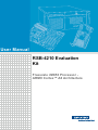
RSB-4210 Evaluation
Kit
Freescale i.MX53 Processor ARM® Cortex™ A8 Architecture
Copyright
The documentation and the software included with this product are copyrighted 2012
by Advantech Co., Ltd. All rights are reserved. Advantech Co., Ltd. reserves the right
to make improvements in the products described in this manual at any time without
notice. No part of this manual may be reproduced, copied, translated or transmitted
in any form or by any means without the prior written permission of Advantech Co.,
Ltd. Information provided in this manual is intended to be accurate and reliable. However, Advantech Co., Ltd. assumes no responsibility for its use, nor for any infringements of the rights of third parties, which may result from its use.
Acknowledgements
ARM is trademarks of ARM Corporation.
Freescale is trademarks of Freescale Corporation.
Microsoft Windows are registered trademarks of Microsoft Corp.
All other product names or trademarks are properties of their respective owners.
Product Warranty (2 years)
Advantech warrants to you, the original purchaser, that each of its products will be
free from defects in materials and workmanship for two years from the date of purchase.
This warranty does not apply to any products which have been repaired or altered by
persons other than repair personnel authorized by Advantech, or which have been
subject to misuse, abuse, accident or improper installation. Advantech assumes no
liability under the terms of this warranty as a consequence of such events.
Because of Advantech’s high quality-control standards and rigorous testing, most of
our customers never need to use our repair service. If an Advantech product is defective, it will be repaired or replaced at no charge during the warranty period. For outof-warranty repairs, you will be billed according to the cost of replacement materials,
service time and freight. Please consult your dealer for more details.
If you think you have a defective product, follow these steps:
1. Collect all the information about the problem encountered. (For example, CPU
speed, Advantech products used, other hardware and software used, etc.) Note
anything abnormal and list any onscreen messages you get when the problem
occurs.
2. Call your dealer and describe the problem. Please have your manual, product,
and any helpful information readily available.
3. If your product is diagnosed as defective, obtain an RMA (return merchandize
authorization) number from your dealer. This allows us to process your return
more quickly.
4. Carefully pack the defective product, a fully-completed Repair and Replacement
Order Card and a photocopy proof of purchase date (such as your sales receipt)
in a shippable container. A product returned without proof of the purchase date
is not eligible for warranty service.
5. Write the RMA number visibly on the outside of the package and ship it prepaid
to your dealer.
RSB-4210 User Manual
Part No. 2002421000
Edition 1
Printed in Taiwan
December 2012
ii
Packing List
Before setting up the system, check that the items listed below are included and in
good condition. If any item does not accord with the table, please contact your dealer
immediately.
RSB-4210 (P/N: RSB-4210CF-A78AAE)
7" LED PANEL 320N 4WR T/S 800X480(G), 97G070V1N0F-2, P/N: 96LEDKA070WV32RB1)
LCD Backlight Cable (P/N: 1700019577)
LVDS Cable (P/N: 1700014418)
Touch Cable (P/N: 1700000194)
SQFlash SD Card SLC 2G, 2CH(-40 ~ 85° C) (P/N: SQF-ISDS2-2G-ETE)
A CABLE SATA 15P/1*4P-2.5 35cm for AIMB-213 (P/N: 1700018785)
M Cable SATA 7P/SATA 7P 8CM C=R 180/180 (P/N:1700004711)
Mini USB Host Cable (P/N: 1700019076)
Mini USB Client Cable (P/N: 1700019077)
USB Type-A Cable (P/N: 1700019129)
ADAPTER 100-240 V 65 W 19 V 3.42 A 9NA0651256 (P/N: 1757003734)
A Cable 2*8P-2.0/SPEAKER*2+DC JACK*3 40CM(P/N: 1700019546-11)
F Cable IDE#2 10P-2.0/D-SUB 9P(M) 25CM (P/N: 1700100250)
Terminal connector 9P Female (P/N: 1654909900)
DVD-ROM for RSB-4210 Evaluation Kit (P/N: 2062421011)
RS-232 and RS-485 cable (P/N: 1700019474)
RS-422 cable (P/N: 1700019476)
Power Cord (Optional)
3 pin Power Cord for USA standard (P/N: 1700001524)
3 pin Power Cord for Europe standard (P/N: 170203183C)
3 pin Power Cord for UK standard (P/N: 170203180A)
Charger Board & Battery (Optional)
A cable 1*6P-2.5/1*6P-2.5 140 mm (P/N: 1700018394)
A cable 2*4P-2.0/2*4P-2.0 90 mm (P/N: 1700018395)
PCM-739 Battery charger Board (P/N: 969K073900E)
Battery 11.1 V 6300 mAh 3S3P (P/N: 1760001300)
iii
RSB-4210 User Manual
Safety Instructions
1.
2.
3.
4.
5.
6.
7.
8.
9.
10.
11.
12.
13.
14.
Read these safety instructions carefully.
Keep this User Manual for later reference.
Disconnect this equipment from any AC outlet before cleaning. Use a damp
cloth. Do not use liquid or spray detergents for cleaning.
For plug-in equipment, the power outlet socket must be located near the equipment and must be easily accessible.
Keep this equipment away from humidity.
Put this equipment on a reliable surface during installation. Dropping it or letting
it fall may cause damage.
The openings on the enclosure are for air convection. Protect the equipment
from overheating. DO NOT COVER THE OPENINGS.
Make sure the voltage of the power source is correct before connecting the
equipment to the power outlet.
Position the power cord so that people cannot step on it. Do not place anything
over the power cord.
All cautions and warnings on the equipment should be noted.
If the equipment is not used for a long time, disconnect it from the power source
to avoid damage by transient overvoltage.
Never pour any liquid into an opening. This may cause fire or electrical shock.
Never open the equipment. For safety reasons, the equipment should be
opened only by qualified service personnel.
If one of the following situations arises, get the equipment checked by service
personnel:
The power cord or plug is damaged.
Liquid has penetrated into the equipment.
The equipment has been exposed to moisture.
The equipment does not work well, or you cannot get it to work according to
the user's manual.
The equipment has been dropped and damaged.
The equipment has obvious signs of breakage.
RSB-4210 User Manual
iv
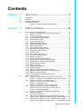
Contents
Chapter
Chapter
1
Overview...............................................1
1.1
1.2
1.3
1.4
Introduction ............................................................................................... 2
Features .................................................................................................... 2
Hardware Specifications ........................................................................... 3
Board Block Diagram ................................................................................ 4
Figure 1.1 RSB-4210 Board Block Diagram ................................ 4
2
H/W Installation....................................5
2.1
Development Kit H/W Installation.............................................................. 6
Figure 2.1 RSB-4210 Development Kit Assembly ....................... 7
2.1.1 RSB-4210 (Part-A)........................................................................ 7
2.1.2 7" LVDS LCD Module (Part-B1).................................................... 7
2.1.3 LCD Backlight Cable (Part-B2) ..................................................... 8
2.1.4 LVDS Cable (Part-B3)................................................................... 8
2.1.5 Touch Cable (Part-B4) .................................................................. 8
2.1.6 SQFlash SD Card (Part-C) ........................................................... 8
2.1.7 SATA Power Cable (Part-D) ......................................................... 8
2.1.8 SATA Cable (Part-E)..................................................................... 8
2.1.9 Mini USB Host Cable (Part-F)....................................................... 8
2.1.10 Mini USB Client Cable (Part-G) .................................................... 8
2.1.11 USB Type-A Cable (Part-H).......................................................... 8
2.1.12 Jumper (Part-I).............................................................................. 8
2.1.13 Null modem cable (Part-J) ............................................................ 8
2.1.14 19 V Power Adapter (Part-K) ........................................................ 8
2.1.15 Power Cord (Part-L)...................................................................... 9
2.1.16 Speaker & Audio Cables (Part-M)................................................. 9
2.1.17 Power Cable for Charger Board (Part-N1).................................... 9
2.1.18 Signal Cable for Charger Board (Part-N2) .................................... 9
2.1.19 Charger Board (Part-N3)............................................................... 9
2.1.20 Battery (Part-N4)........................................................................... 9
2.1.21 Keypad Cable (Part-O1) ............................................................... 9
2.1.22 Keypad (Part-O2).......................................................................... 9
2.1.23 Cable for Suspend/Reset Button (Part-P)..................................... 9
2.1.24 COM Port Cable (D-SUB 9P to Housing) (Part-Q) ....................... 9
2.1.25 RS-232 Loopback (Part-R) ........................................................... 9
2.1.26 Terminal Block for CAN/RS-485 (Part-S)...................................... 9
RSB-4210 Connectors ............................................................................ 10
2.2.1 Wafer for 4-wire Resistive Type Touch Screen (CN1)............... 10
Figure 2.2 Wafer for 4-wire Resistive Type Touch Screen ....... 11
2.2.2 Phoenix Connector for CAN Bus (CN2)...................................... 11
Figure 2.3 Phoenix Connector for CAN Bus .............................. 11
Figure 2.4 CAN Application ....................................................... 12
Figure 2.5 Schematics of CAN on RSB-4210............................ 12
2.2.3 Phoenix Connector for COM3, RS-485 (CN3) ............................ 12
Figure 2.6 Phoenix Connector for COM3, RS-485 .................... 12
Figure 2.7 RS-485 Application................................................... 13
Figure 2.8 Schematics of RS-485 on RSB-4210 ....................... 13
2.2.4 System Bus (CN4) ...................................................................... 13
Figure 2.9 System Bus .............................................................. 13
2.2.5 Pin Header for COM5, RS-232 (TX/RX/RTS/CTS) (CN5) .......... 14
Figure 2.10Pin Header for COM5, RS-232 (TX/RX/RTS/CTS) .. 14
2.2.6 Pin Header for COM4, 3.3V TTL (TX/RX/RTS/CTS) (CN6)........ 15
Figure 2.11Pin Header for COM4, 3.3V TTL (TX/RX/RTS/CTS) 15
2.2
v
RSB-4210 User Manual
2.2.7
2.2.8
2.2.9
2.2.10
2.2.11
2.2.12
2.2.13
2.2.14
2.2.15
2.2.16
2.2.17
2.2.18
2.2.19
2.2.20
2.2.21
2.2.22
2.2.23
2.2.24
2.2.25
2.2.26
2.2.27
2.2.28
2.2.29
2.2.30
2.2.31
2.2.32
2.2.33
2.2.34
RSB-4210 User Manual
Pin Header for I2S (CN7)............................................................ 15
Figure 2.12Pin Header for I2S.................................................... 15
LVDS0 LCD Connector (CN8) .................................................... 16
Figure 2.13LVDS0 LCD Connector ............................................ 16
Pin Header for COM1, RS-232 (TX/RX) (CN9) .......................... 17
Figure 2.14Pin Header for COM1, RS-232 (TX/RX)................... 17
Pin Header for SD2 (CN10) ........................................................ 17
Figure 2.15Pin Header for SD2 .................................................. 18
Wafer for Backlight Power and Controller (CN11) ...................... 18
Figure 2.16Wafer for Backlight Power and Controller ................ 18
MiniPCIe Connector-Latch (CN12) and Connector (CN13)........ 19
Figure 2.17MiniPCIe Connector-Latch (CN12) and Connector
(CN13)...................................................................... 19
LVDS1 LCD Connector (CN14) .................................................. 20
Figure 2.18LVDS1 LCD Connector ............................................ 20
Pin Header for Jtag (CN15) ........................................................ 21
Figure 2.19Pin Header for Jtag .................................................. 21
Wafer for SATA power (CN16) ................................................... 21
Figure 2.20Wafer for SATA power ............................................. 21
Wafer for Power ON/OFF (CN17)............................................... 22
Figure 2.21Pin Header for Power Button.................................... 22
Ethernet LAN1&2 Connector (CN18).......................................... 22
Figure 2.22Ethernet LAN1 & LAN2 Connector........................... 23
Wafer for Coin Battery (CN19).................................................... 23
Figure 2.23Wafer for Coin Battery.............................................. 23
SIM Card slot (CN20) ................................................................. 24
Figure 2.24SIM Card slot............................................................ 24
Pin Header for Reset (RST_BTN1) ............................................ 24
Figure 2.25Pin Header for Reset................................................ 24
Pin Header for Suspend (SUS_BTN1) ....................................... 25
Figure 2.26Pin Header for Suspend ........................................... 25
Pin Header for Matrix Keypad (KEYPAD1)................................. 25
Figure 2.27Pin Header for Matrix Keypad .................................. 26
Pin Header for I2C/SPI (CN21)................................................... 26
Figure 2.28Pin Header for I2C/SPI............................................. 26
Pin Header for 20x pins GPIO (GPIO1)...................................... 27
Figure 2.29Pin Header for GPIO ................................................ 27
SATA Connector (SATA_CN1)................................................... 28
Figure 2.30SATA Connector ...................................................... 28
Pin Header for USB_HUB1 (USB1)............................................ 28
Figure 2.31Pin Header for USB_HUB1 ...................................... 28
Wafer for Battery Charger Board - Power (BAT_CN1) ............... 29
Figure 2.32Wafer for Battery Charger Board - Power ................ 29
Wafer for Battery Charger Board -Control Signal (BAT_CN2).... 29
Figure 2.33Wafer for Battery Charger Board - Control Signal.... 29
USB OTG MINI-AB Connector (USB_OTG1)............................. 30
Figure 2.34USB OTG MINI-AB Connector ................................. 30
USB HUB_2&3 (Standard Type-A) (USB2) ................................ 30
Figure 2.35USB CSB_HUB_2&3 (Standard Type-A) ................. 30
VGA Connector (CRT1).............................................................. 31
Figure 2.36VGA Connector (D-SUB15)...................................... 31
HDMI Connector (HDMI_CN1) ................................................... 31
Figure 2.37HDMI Connector....................................................... 31
Box Header for LINE-OUT, LINE-IN, MIC-IN and L&R Speakers
(AUDIO1) .................................................................................... 32
Figure 2.38Box Header for LINE-OUT, LINE-IN, MIC-IN and L&R
Speakers .................................................................. 32
D-Sub9 Connector for COM2, RS-232 (TX/RX/RTS/ CTS)
(COM1) ....................................................................................... 32
Figure 2.39D-Sub9 Connector for COM2, RS-232 (TX/RX/RTS/
vi
Chapter
2.3
CTS) ......................................................................... 32
2.2.35 DC-IN Power Jack(DCIN1) ......................................................... 33
Figure 2.40DC-IN Power Jack .................................................... 33
2.2.36 SD Card Slot (SD1)..................................................................... 33
Figure 2.41SD card Slot ............................................................. 33
Mechanical .............................................................................................. 34
2.3.1 Connector Location..................................................................... 34
Figure 2.42RSB-4210 Connector Position (Top) ........................ 34
Figure 2.43RSB-4210 Connector Position (Bottom)................... 34
2.3.2 RSB-4210 Board Dimension....................................................... 35
Figure 2.44RSB-4210 Board Dimension .................................... 35
3
Software Functionality ......................37
3.1
The Bootloader........................................................................................ 38
3.1.1 Communication settings.............................................................. 38
3.1.2 Startup of the bootloader ............................................................ 38
3.1.3 Change Display Output Resolution............................................. 39
WinEC7 Startup Procedure..................................................................... 40
3.2.1 WinEC7 Bootup Steps ................................................................ 41
3.2.2 Booting form On Board Flash or SATA....................................... 44
Utilities..................................................................................................... 44
3.3.1 Test Utility ................................................................................... 44
Figure 3.1 Test Utility................................................................. 44
3.3.2 Startup Execution........................................................................ 45
3.3.3 Platform Setting .......................................................................... 45
Figure 3.2 General Information.................................................. 45
Figure 3.3 Display Configuration ............................................... 46
Figure 3.4 Watchdog Timer ....................................................... 47
Figure 3.5 Audio Settings .......................................................... 48
Figure 3.6 Miscellaneous Settings............................................ 49
Network ................................................................................................... 50
Figure 3.7 Networking via Ethernet ........................................... 50
BSP Carried Tools .................................................................................. 50
3.5.1 Display and Video Testing Tools ................................................ 50
Figure 3.8 Display Driver GUI.................................................... 51
3.5.2 AudioRouting .............................................................................. 53
3.5.3 Graphics Processing Unit Testing Tools..................................... 53
Figure 3.9 Tiger Test ................................................................. 54
Figure 3.10Cube Test ................................................................. 54
Figure 3.11Triangle Test............................................................. 55
3.5.4 Application Tool for USB Device Class Select............................ 55
Figure 3.12USB Device Class Switch User Interface ................. 55
Binary BSP introduction .......................................................................... 56
3.6.1 Build WinEC7 OS Image............................................................. 56
3.6.2 Windows CE Startup Procedure ................................................. 57
3.6.3 U-boot development.................................................................... 57
SDK introduction ..................................................................................... 57
3.7.1 Create a new Windows EC 7 project .......................................... 57
3.7.2 How to use SUSI......................................................................... 59
Connect Device with PC with Activesync................................................ 61
Implement Break Points .......................................................................... 63
SUSI Library............................................................................................ 64
3.10.1 Package Contents....................................................................... 67
3.10.2 Additional Programs.................................................................... 68
Figure 3.13General Information.................................................. 68
3.10.3 SUSI API Programmer's Documentation .................................... 75
3.2
3.3
3.4
3.5
3.6
3.7
3.8
3.9
3.10
vii
RSB-4210 User Manual
Appendix A
API Error Code .................................. 93
A.1
A.2
A.3
Function Index Code............................................................................... 94
Library Error Code .................................................................................. 96
Driver Error Code.................................................................................... 98
RSB-4210 User Manual
viii
Chapter
1
1
Overview
This chapter briefly introduces the
RSB-4210 Platform and RSB-4210
Evaluation Kit.
1.1 Introduction
In order to offer potential RISC-based Design-to-Order-Service (DTOS) project customers with a more efficient and low risk evaluation tool, Advantech provides a variety of RISC-based evaluation kits. Before DTOS projects kick-off, customers can
check their designs with these kits in detail more easily. The evaluation kits are
already equipped with all of the necessary H/W and S/W parts which customers will
need, thus reducing design effort and speeding up application development.
The RSB-4210 is designed as a single board computer (SBC) solution, with a Freescale i.MX53 processor based on ARM® Cortex™ A8 architecture, which is a complete 32-bit, up to 1GHz speed SoC engine. It provides customers with a high
performance board subsystem based on ARM® Cortex™ A8 which is ready-to-run,
compact, and easy-to-expand in order to meet customers' versatile needs. With flexible I/O interfaces and complete hardware and software solutions, RSB-4210 is a fast
time-to-market platform for customers to develop their applications and products easily without considering system integration.
The RSB-4210 Evaluation Kit is a complete system designed for customers to evaluate RSB-4210. It integrates all of the solutions that developers will need into a package for project evaluation, application development, and solution feasibility testing
that decreases lead-time and lowers initial expense. All the functions included in the
kit have been certified under Linux, ensuring that project development is more simple, less risky and easier to implement.
1.2 Features
RSB-4210 incorporates a Freescale i.MX53 Processor - ARM® Cortex™ A8 architecture as its SoC solution. The main features of this platform are a heatsink-less and
compact design, and great reliability and power management making it suitable for
the following applications:
Economical HMI (Human Machine Interface)
Self Service / Access Control
Fleet management / Navigation
Hand-held data collector
And the main features of Freescale i.MX53 processor are shown as follows:
ARM® Cortex™-A8 1GHz high performance processor
Supports OpenGL ES 2.0 and OpenVG® 1.1 hardware accelerators
Supports full HD 1080p video decode and HD 720p video encode hardware
engine Freescale Smart Speed® Technology support low power consumption
I/O through 3.3 V I/O voltage and wide working temperature by industrial design
concept
Rich I/O for high expansion capability: UART(5), Dual LVDS, Audio, USB Host,
USB OTG, Dual LAN, SD(2), SATA(1), GPIO(20), I2C(2), SPI(1), I2S(1),
CAN(1), Keypad 6X6, Touch, Mini PCI-E and System Bus
Supports SATA storage interface and CAN bus for vehicle application
Supports Android2.3, Embedded Linux2.6 and Windows Embedded Compact 7
Support wide working temperature -40 ~ 85° C operation temperature
(optional)
RSB-4210 User Manual
2
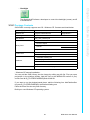
Item
Chapter 1
1.3 Hardware Specifications
Description
Kernel
Freescale i.MX53 1GHz (ARM Cortex A8)
2D/3D Accelerators
Support OpenGL ES 2.0 and OpenVG™ 1.1 hardware accelerators
System RAM
512 MB (Optional: 256 MB)
Onboard Flash
2 GB (Optional: None)
RTC
Yes
Watchdog Timer
Yes
Reset
H/W reset & S/W reset
I/O
COM
COM 1, RS-232, 2–wire(TX/RX), Pin header, (Debug port)
COM 2, RS-232, D-Sub9 Connector(TX/RX/RTS/CTS)
COM 3, RS-485, 2-pin Phoenix Connector
COM 4, 3.3 V TTL, 4–wire(TX/RX/RTS/CTS), Pin header
COM 5, RS-232, 4–wire(TX/RX/RTS/CTS), Pin header
Ethernet LAN
2 x 10/100 BASE-T (RJ-45)
USB Port
3 x USB 2.0 (High speed)
USB OTG
1 x USB 2.0 OTG (High speed)
SD/MMC
2 x SDIO/MMC interface (SD slot x 1+ pin header x 1)
Mini PCI-E
1 x (Controlled by USB interface only)
SIM Card slot
1
SATA
1
Touch Screen
1 x 4 - wire resistive type interface
System Bus
Yes (Address: 25 pins, data: 16 pins)
2
I C Interface
2
I2S Interface
1
SPI Interface
1
CAN BUS
1
Hotkey/
Matrix keypad
Support 6 x 6 matrix keypad
GPIO
20 pins 3.3 V TTL level GPIOs
Buzzer control
Yes
Multimedia
Graphic Chip
CPU internal LCD controller
LCD Resolution
Default: 800 x 480 7” WVGA
Optional: 320 x 240 ~ 1920 x 1080
Dual LVDS
2 x 24-bit LVDS
HDMI
1 x (Co-lay with VGA)
VGA
1 x (Co-lay with HDMI)
Brightness/
Backlight Control
Yes
Audio
Line-in(Stereo),Line-out(Stereo),Speak-Out(Stereo)&Mic-in(Mono)
Power
DC-input
9 ~ 24 V 5%
Battery Support
Yes (With external battery and charger board thru connector)
3
RSB-4210 User Manual
Overview
CPU
Power Consumption
Normal Run ~2.3 W
Full Run ~3.8 W
Power Control
1 x Power ON/OFF Pin header
1 x H/W reset Pin header
1 x Suspend Pin header
Power Management
-Standard mode
-Idle mode
Mechanical and Environmental
Board size
146 x 102 x 20 mm (PCB thickness 1.6 mm; 8 layer)
Weight
110 g
Operation Temperature
0 ~ 60° C (32 ~ 140° F)
(-40 ~ 85° C by component change)
Operating Humidity
5% ~ 95% Relative Humidity, non condensing
Vibration
3.5 G, 1000 times
Others
RoHS
Yes
Certification
CE/FCC Class A
O.S
Embedded Linux 2.6.35 (Default), Android 2.3.4,
and Windows Embedded Compact 7
1.4 Board Block Diagram
Figure 1.1 RSB-4210 Board Block Diagram
RSB-4210 User Manual
4
Chapter
2
2
H/W Installation
This chapter introduces the setup
procedures of the RSB-4210 hardware, including instructions on
setting jumpers and connecting
peripherals, switches, indicators
and mechanical drawings.
Be sure to read all safety precautions before you begin this installation procedure.
2.1 Development Kit H/W Installation
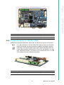
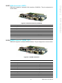
The Figure 2-1 is RSB-4210 Evaluation Kit Assembly, and the detail descriptions with
Advantech P/N are shown as below.
Item
Description
Advantech P/N
Part-A
RSB-4210
(P/N: RSB-4210CF-A78AAE)
Part-B1
7” LCD-LED Backlight, LVDS, 800x480, T/S,
97G070V1N0F-2
(P/N: 96LEDK-A070WV32RB1)
Part-B2
LCD Backlight Cable
(P/N: 1700019577)
Part-B3
LVDS Cable
(P/N: 1700014418)
Part-B4
Touch Cable
(P/N: 1700000194)
Part-C
SQFlash SD Card, SLC 2GB, (-40~85°C)
(P/N: SQF-ISDS2-2G-ETE)
Part-D
SATA Power Cable
(P/N: 1700018785)
Part-E
SATA Cable
(P/N: 1700004711)
Part-F
Mini USB Host Cable
(P/N: 1700019076)
Part-G
Mini USB Client Cable
(P/N: 1700019077)
Part-H
USB Type-A Cable
(P/N: 1700019129)
Part-I
Mini Jumper
(P/N:1653302122)
Part-J
Null modem cable
(P/N: 1700091002)
Part-K
ADAPTER, 100-240V, 19V, 3.42A.
(P/N: 1757003734)
Part-L
3 pin Power Cord (USA Standard) [Optional]
3 pin Power Cord (Europe standard) [Optional]
3 pin Power Cord (UK standard) [Optional]
(P/N: 1700001524)
(P/N: 170203183C)
(P/N: 170203180A)
Part-M
Speaker & Audio Cables
(P/N: 1700019546-11)
Part-N1
Power Cable for Charger Board [Optional]
(P/N: 1700018394)
Part-N2
Signal Cable for Charger Board [Optional]
(P/N: 1700018395)
Part-N3
Charger Board [Optional]
(P/N: 969K073900E)
Part-N4
Battery [Optional]
(P/N: 1760001300)
Part-O1
8*8 Keypad Cable [Optional]
(P/N: 1703200180)
Part-O2
8*8 Keypad [Optional]
(P/N: 96969315A0E)
Part-P
Suspend/Reset button cable [Optional]
(P/N:1700003414)
Part-Q
COM Port Cable
(P/N: 1700100250)
Part-R
RS-232 Loopback
(P/N: 1654909900)
Part-S
Terminal Block for CAN/RS-485
(P/N: 1652002209)
RSB-4210 User Manual
6
Chapter 2
H/W Installation
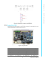
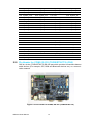
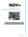
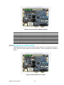
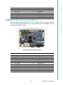
Figure 2.1 RSB-4210 Development Kit Assembly
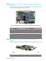
2.1.1 RSB-4210 (Part-A)
RSB-4210 is a cost-effective, low-power, and high-performance SBC (Single Board
Computer) without a heatsink, geared to satisfy the needs of industrial computing
applications. Based on the Freescale i.MX53 Processor - ARM® Cortex™ A8 architecture, RSB-4210 comes with DDR3, and iNAND flash. RSB-4210 offers convenient
connector layout, simple assembly, multiple common I/Os, and includes dual 10/
100Mbps Ethernet, three USB (Universal Serial Bus) 2.0 connectors and five serial
ports for easy system expansibility.
2.1.2 7" LVDS LCD Module (Part-B1)
The 7.0 inch Color TFT-LCD Module uses a 4-wire resistive type touch sensor. The
module is designed with a wide viewing angle; wide operating temperature and long
life LED backlight which is well suited for Industrial Applications. An LED driving
board for backlight unit is included in this panel and the structure of the LED units is
replaceable. It also has a built in timing controller and LVDS interface. The display
supports the WVGA (800 (H) x 480(V)) screen format and 16.2 M colors (RGB
24bits) or 262 K (RGB 18 bits) selectable.
7
RSB-4210 User Manual
2.1.3 LCD Backlight Cable (Part-B2)
The LVDS backlight cable connects RSB-4210 (CN11) with the LCD backlight connector of 7" LVDS LCD Module.
2.1.4 LVDS Cable (Part-B3)
The LVDS cable connects RSB-4210 LVDS0 connector (CN8) with the LCD signal
connector of 7" LVDS LCD Module.
2.1.5 Touch Cable (Part-B4)
The touch cable connects RSB-4210 (CN1) with the touch connector of 7" LVDS LCD
Module.
2.1.6 SQFlash SD Card (Part-C)
The SQFlash SD card is a standard SD device. It is the flash-based solid-state drive
available and uses SLC NAND flash memory, making it ideal as an embedded SSD
solution. It connects on SD1 of RSB-4210.
2.1.7 SATA Power Cable (Part-D)
The SATA power cable provides the power signal for SATA HDD by connecting RSB4210 (CN16) and the SATA HDD.
2.1.8 SATA Cable (Part-E)
The SATA cable provides the control signal with SATA HDD by connecting RSB-4210
(SATA_CN1) with the SATA HDD.
2.1.9 Mini USB Host Cable (Part-F)
The mini USB Host cable connects RSB-4210 (USB_OTG1) with one USB client
device. For example, USB mouse/keyboard.
2.1.10 Mini USB Client Cable (Part-G)
The mini USB Client cable connects RSB-4210 (USB_OTG1) with PC or NB.
2.1.11 USB Type-A Cable (Part-H)
The USB extend cable provide Type-A for USB device. For example, USB mouse/
keyboard.
2.1.12 Jumper (Part-I)
When plug-in the adapter with the wafer (CN17) shorted by this jumper, the system
will power-on.
2.1.13 Null modem cable (Part-J)
The null modem cable connects RSB-4210 COM ports with a serial device.
2.1.14 19 V Power Adapter (Part-K)
The AC-to-DC power device provides a 19 V DC output (65 W max) with constant
voltage sources (100 V ~ 240 V).
RSB-4210 User Manual
8
3P Power Cord (USA, Europe or UK standard) for 19 V Power Adapter AC input.
2.1.16 Speaker & Audio Cables (Part-M)
The cable connects with RSB-4210 (AUDIO1) and LINE-OUT, LINE-IN, MIC-IN and
L&R Speakers.
Chapter 2
2.1.15 Power Cord (Part-L)
2.1.17 Power Cable for Charger Board (Part-N1)
2.1.18 Signal Cable for Charger Board (Part-N2)
The cable provides the control signal for charger board. It connects RSB-4210
(BAT_CN2) with the charger board (CN1).
2.1.19 Charger Board (Part-N3)
The charger board provides 12v power to charge the battery when plug-in a 19v
adapter, and RSB-4210 can read the battery status through this charger board.
Note!
It is necessary to use 19v adapter for charger board rather than 12v.
2.1.20 Battery (Part-N4)
The battery can provide the power with RSB-4210 without any adapter.
2.1.21 Keypad Cable (Part-O1)
The keypad cable connects RSB-4210 (KEYPAD1) with the keypad.
2.1.22 Keypad (Part-O2)
8*8 arrays of 64 normally open single-pole switches. (6*6 region of keypad are available when using RSB-4210.)
2.1.23 Cable for Suspend/Reset Button (Part-P)
The cable is used to extend the Suspend/Reset function by a specific button.
2.1.24 COM Port Cable (D-SUB 9P to Housing) (Part-Q)
The cable is used to extend COM port 9pin header from RSB-4210 to D-SUB 9P
serial port connector.
2.1.25 RS-232 Loopback (Part-R)
The terminal connector 9P female is used to test RS-232 loopback function.
2.1.26 Terminal Block for CAN/RS-485 (Part-S)
The terminal block can be extended with extra two cables to connect RSB-4210
CAN/RS-485 function with the others CAN/RS-485 devices.
9
RSB-4210 User Manual
H/W Installation
The cable provides the power for charger board. It connects RSB-4210 (BAT_CN1)
with the charger board (CN2).
2.2 RSB-4210 Connectors
The following table shows the connector list of RSB-4210.
2.2.1
Connector
Description
CN 1
Wafer for 4-wire Resistive Type Touch Screen
CN 2
Phoenix Connector for CAN Bus
CN 3
Phoenix Connector for COM3, RS-485
CN 4
System Bus
CN 5
Pin Header for COM5, RS-232 (TX/RX/RTS/CTS)
CN 6
Pin Header for COM4, 3.3V TTL (TX/RX/RTS/CTS)
CN 7
Pin Header for I2S
CN 8
LVDS0 LCD Connector
CN 9
Pin Header for COM1, RS-232 (TX/RX)
CN 10
Pin Header for SD2
CN 11
Wafer for Backlight Power and Controller
CN 12
MiniPCIe Connector-Latch
CN 13
MiniPCIe Connector
CN 14
LVDS1 LCD Connector
CN 15
Pin Header for Jtag
CN 16
Wafer for SATA Power
CN 17
Wafer for Power ON/OFF
CN 18
Ethernet LAN1&2 Connector
CN 19
Wafer for Coin Battery
CN 20
SIM Card Slot
RST_BTN1
Pin Header for Reset
SUS_BTN1
Pin Header for Suspend
KEYPAD1
Pin Header for Matrix Keypad
CN21
Pin Header for I2C/SPI
GPIO1
Pin Header for 20x pins GPIO
SATA_CN1
SATA Connector
USB1
Pin Header for USB_HUB1
BAT_CN1
Wafer for Battery Charger Board – Power
BAT_CN2
Wafer for Battery Charger Board – Control Signal
USB_OTG1
USB OTG MINI-AB Connector
USB2
USB_HUB_2&3 (Standard Type-A)
CRT1
VGA Connector
HDMI_CN1
HDMI Connector
AUDIO1
Box Header for LINE-OUT, LINE-IN, MIC-IN and L&R Speakers
COM1
D-Sub9 Connector for COM2, RS-232 (TX/RX/RTS/CTS)
DCIN1
DC-IN Power Jack
SD1
SD Card Slot
Wafer for 4-wire Resistive Type Touch Screen (CN1)
The touch screen interface performs all sampling, averaging, ADC range checking,
and control for a wide variety of analog resistive touch screens. This controller only
interrupts the processor when a meaningful change occurs.
RSB-4210 User Manual
10
Chapter 2
Pin
Description
Pin
Description
1
Touch_Y-
2
Touch_Y+
3
Touch_X-
4
Touch_X+
2.2.2 Phoenix Connector for CAN Bus (CN2)
RSB-4210 supports one CAN bus, while CN2 is a phoenix connector for CAN bus.
Note!
For CAN applications, the two ends of the cable will have a termination
resistor connected across the two wires. Without termination resistors,
reflections of fast driver edges can cause multiple data edges that can
cause data corruption. Please refer to Figure 2.4 and Figure 2.5 to adding a termination resistor (120 ohms) on your end device (R271 of RSB4210, default is none) to avoid this situation.
Figure 2.3 Phoenix Connector for CAN Bus
Pin
Description
Pin
Description
1
CAN_D+
2
CAN_D-
11
RSB-4210 User Manual
H/W Installation
Figure 2.2 Wafer for 4-wire Resistive Type Touch Screen
Figure 2.4 CAN Application
Figure 2.5 Schematics of CAN on RSB-4210
2.2.3 Phoenix Connector for COM3, RS-485 (CN3)
RSB-4210 supports one RS-485 interface, while CN3 is a phoenix connector for RS485.
Note!
For RS-485 applications, the two ends of the cable will have a termination resistor connected across the two wires. Without termination resistors, reflections of fast driver edges can cause multiple data edges that
can cause data corruption. Please refer to Figure 2.7 and Figure 2.8 to
adding a termination resistor (120 ohms) on your end device (R289 of
RSB-4210, default is 120 ohms) to avoid this situation.
Figure 2.6 Phoenix Connector for COM3, RS-485
Pin
Description
Pin
Description
1
RS485_TXD-
2
RS485_TXD+
RSB-4210 User Manual
12
Chapter 2
Figure 2.7 RS-485 Application
H/W Installation
Figure 2.8 Schematics of RS-485 on RSB-4210
2.2.4 System Bus (CN4)
The RSB-4210 provides system bus via PCI104+ connector for extended device use.
The pin assignments are shown below in Fig 2.9.
Figure 2.9 System Bus
Pin Description
Pin Description
Pin Description
Pin Description
A1
N/C
B1
GND
C1
N/C
D1
N/C
A2
GND
B2
N/C
C2
DIO_3V3
D2
DIO_3V3
A3
EX_GPIO_8
B3
IMX_GPIO4
C3
IMX_GPIO3
D3
IMX_GPIO2
A4
N/C
B4
N/C
C4
DIO_3V3
D4
DIO_3V3
A5
SysBus_A0
B5
SysBus_A1
C5
SysBus_A15
D5
SysBus_A14
A6
SysBus_A2
B6
SysBus_A3
C6
SysBus_A13
D6
SysBus_A12
13
RSB-4210 User Manual
A7
SysBus_A4
B7
SysBus_A5
C7
SysBus_A11
D7
SysBus_A10
A8
SysBus_A6
B8
SysBus_A7
C8
SysBus_A9
D8
SysBus_A8
A9
SysBus_A16
B9
SysBus_A17
C9
SysBus_A24
D9
N/C
A10 SysBus_A18
B10 SysBus_A19
C10 N/C
D10 SysBus_OE
A11 SysBus_A20
B11 SysBus_A21
C11 SysBus_RW
D11 GND
A12 SysBus_A22
B12 SysBus_A23
C12 N/C
D12 N/C
A13 DIO_3V3
B13 N/C
C13 SysBus_CS0
D13 SysBus_CS1
A14 SysBus_D0
B14 SysBus_D1
C14 SysBus_D15
D14 SysBus_D14
A15 SysBus_D2
B15 SysBus_D3
C15 SysBus_D13
D15 SysBus_D12
A16 SysBus_D4
B16 SysBus_D5
C16 SysBus_D11
D16 SysBus_D10
A17 SysBus_D6
B17 SysBus_D7
C17 SysBus_D9
D17 SysBus_D8
A18 N/C
B18 N/C
C18 N/C
D18 N/C
A19 N/C
B19 N/C
C19 N/C
D19 N/C
A20 N/C
B20 N/C
C20 N/C
D20 N/C
A21 N/C
B21 N/C
C21 N/C
D21 N/C
A22 N/C
B22 N/C
C22 SysBus_BCLK
D22 GND
A23 N/C
B23 N/C
C23 N/C
D23 GND
A24 N/C
B24 N/C
C24 SysBus_EB1
D24 DIO_3V3
A25 N/C
B25 N/C
C25 N/C
D25 DIO_3V3
A26 SysBus_nEB0
B26 N/C
C26 N/C
D26 N/C
A27 N/C
B27 SysBus_LBA
C27 5 V_EXT
D27 5V_EXT
A28 SysBus_WP
B28 N/C
C28 SysBus_Wait
D28 N/C
A29 N/C
B29 N/C
C29 N/C
D29 N/C
A30 SysBus_Wait
B30 N/C
C30 GND
D30 N/C
2.2.5 Pin Header for COM5, RS-232 (TX/RX/RTS/CTS) (CN5)
CN5 is a 4-wire (TX/RX/RTS/CTS) RS-232 port which provides connections between
serial devices (For example, GPS, GSM and Bluetooth devices etc.) or a communication network.
Figure 2.10 Pin Header for COM5, RS-232 (TX/RX/RTS/CTS)
RSB-4210 User Manual
14
Description
Pin
Description
1
N/C
2
N/C
3
COM5_RXD
4
COM5_RTS
5
COM5_TXD
6
COM5_CTS
7
N/C
8
N/C
9
GND
10
N/C
CN6 is a 4-wire (TX/RX/RTS/CTS) 3.3 V TTL signal which provides connections
between serial devices (For example, GPS, GSM and Bluetooth devices etc.) or a
communication network.
Figure 2.11 Pin Header for COM4, 3.3V TTL (TX/RX/RTS/CTS)
2.2.7 Pin Header for I2S (CN7)
RSB-4210 provides one I2S interface for users to expand their applications, and CN7
is the pin header for the I2S interface.
Figure 2.12 Pin Header for I2S
15
RSB-4210 User Manual
H/W Installation
2.2.6 Pin Header for COM4, 3.3V TTL (TX/RX/RTS/CTS) (CN6)
Chapter 2
Pin
Pin
Description
Pin
Description
1
AUDIO_CLK
2
AUD3_TXD
3
AUD3_TXC
4
N/C
5
AUD3_TXFS
6
N/C
7
AUD3_RXD
8
N/C
9
GND
10
DIO_3V3
2.2.8 LVDS0 LCD Connector (CN8)
RSB-4210 supports dual LVDS LCD Interfaces (24+24 bit), in which CN8 is LVDS0
(24-bit) while CN14 is LVDS1 (24-bit). The pin assignment of LVDS0 (CN8) is shown
as below.
Figure 2.13 LVDS0 LCD Connector
Pin
Description
Pin
Description
1
3.3 V
2
3.3 V
3
3.3 V
4
3.3 V
5
LVDS0_TX0-
6
LVDS0_TX0+
7
GND
8
LVDS0_TX1-
9
LVDS0_TX1+
10
GND
11
LVDS0_TX2-
12
LVDS0_TX2+
13
GND
14
LVDS0_CLK-
15
LVDS0_CLK+
16
GND
17
3.3 V
18
N/C
19
LVDS0_TX3-
20
LVDS0_TX3+
RSB-4210 User Manual
16
CN9 is a 2-wire (TX/RX) RS-232 port which provides connections between serial
devices (For example, GPS, GSM and Bluetooth devices etc.) or a communication
network.
Chapter 2
2.2.9 Pin Header for COM1, RS-232 (TX/RX) (CN9)
H/W Installation
Figure 2.14 Pin Header for COM1, RS-232 (TX/RX)
Pin
Description
Pin
Description
1
N/C
2
N/C
3
COM1_RXD
4
N/C
5
COM1_TXD
6
N/C
7
N/C
8
N/C
9
GND
10
N/C
2.2.10 Pin Header for SD2 (CN10)
The SD/MMC Slots are 3.3 V powered, which are able to be extended for SD slot
module and SDIO interface module with the following features:
Fully compatible with the MMC system specification version 3.2
Compatible with the SD Memory Card specification 1.01, and SD I/O specification 1.1 with 1/4 channel(s)
Block-based data transfer between MMC card and SDHC (stream mode not
supported)
100 Mbps maximum data rate in 4-bit mode, SD bus clock up to 25MHz
17
RSB-4210 User Manual
Figure 2.15 Pin Header for SD2
Pin
Description
Pin
Description
1
GND
2
GND
3
SD4_DATA1
4
SD4_CLK
5
SD4_DATA0
6
SD4_CMD
7
SD4_DATA3
8
SD4_CD
9
SD4_DATA2
10
3V3
11
N/C
12
N/C
2.2.11 Wafer for Backlight Power and Controller (CN11)
This wafer provides DC +12 V, DC +5 V, back-light on/off control signal and 0 ~ 5 V
PWM dimming control to inverter. We suggest users choose an inverter so that dimming control is by PWM to fit development kit design.
Figure 2.16 Wafer for Backlight Power and Controller
RSB-4210 User Manual
18
Description
Pin
Description
1
GND
2
GND
3
BLK_PWR_EN
4
BLK_PWR_EN
5
Brightness
6
PWM1
7
12 V
8
5V
Chapter 2
Pin
2.2.12 MiniPCIe Connector-Latch (CN12) and Connector (CN13)
Figure 2.17 MiniPCIe Connector-Latch (CN12) and Connector (CN13)
Pin
Description
Pin
Description
1
nWAKE
2
DIO_3V3
3
N/C
4
N/C
5
N/C
6
IO_1V5
7
nCLKREQ
8
UIM_PWR
9
GND
10
UIM_DATA
11
PCIe_CLK_N
12
UIM_CLK
13
PCIe_CLK_P
14
UIM_RESET
15
GND
16
UIM_VPP
17
N/C
18
GND
19
N/C
20
N/C
21
GND
22
nRESET_OUT
23
PCIe_RX0_N
24
DIO_3V3
25
PCIe_RX0_P
26
GND
27
GND
28
IO_1V5
29
GND
30
PCIe_SMBCLK
31
PCIe_TX0_N
32
PCIe_SMBDAT
33
PCIe_TX0_P
34
GND
35
GND
36
USB_HUB4_D-
37
GND
38
USB_HUB4_D+
19
RSB-4210 User Manual
H/W Installation
RSB-4210 supports a MiniPCIe Interface. The pin assignment is shown below.
39
N/C
40
GND
41
N/C
42
LED_WWAN
43
GND
44
LED_WLAN
45
N/C
46
LED_WPAN
47
N/C
48
IO_1V5
49
N/C
50
GND
51
N/C
52
DIO_3V3
53
N/C
54
N/C
55
GND
56
GND
2.2.13 LVDS1 LCD Connector (CN14)
RSB-4210 supports dual LVDS LCD Interfaces (24+24bit), in which CN8 is LVDS0
(24 bit) while CN14 is LVDS1 (24 bit). The pin assignment of LVDS1 (CN14) is shown
below.
Figure 2.18 LVDS1 LCD Connector
Pin
Description
Pin
Description
1
5V
2
5V
3
5V
4
5V
5
LVDS1_TX0-
6
LVDS1_TX0+
7
GND
8
LVDS1_TX1-
9
LVDS1_TX1+
10
GND
11
LVDS1_TX2-
12
LVDS1_TX2+
13
GND
14
LVDS1_CLK-
15
LVDS1_CLK+
16
GND
17
N/C
18
N/C
19
LVDS1_TX3-
20
LVDS1_TX3+
RSB-4210 User Manual
20
RSB-4210 provides one Jtag interface for debugging CPU. CN15 is the pin header
for Jtag interface.
H/W Installation
Figure 2.19 Pin Header for Jtag
Pin
Description
Pin
Description
1
JTAG_TCK
2
GND
3
JTAG_TMS
4
GND
5
JTAG_TDO
6
GND
7
JTAG_TDI
8
IO_3V3
9
JTAG_TRST
10
N/C
2.2.15 Wafer for SATA power (CN16)
CN16 provides DC +5 V for SATA device. The pin assignment is shown as below.
Figure 2.20 Wafer for SATA power
21
Chapter 2
2.2.14 Pin Header for Jtag (CN15)
RSB-4210 User Manual
Pin
Description
Pin
Description
1
SATA_5 V
2
GND
3
GND
4
N/C
2.2.16 Wafer for Power ON/OFF (CN17)
When plug-in the adapter with CN17 shorted by a jumper, the system will power-on.
Or you can connect this wafer with an external button to control the power ON/OFF.
Note!
If your system cannot power-on with an adapter, please check this
wafer in advance. There should be a jumper or external power switch on
the wafer.
Figure 2.21 Pin Header for Power Button
Pin
Description
Pin
Description
1
PWR_BTN+
2
PWR_BTN-
2.2.17 Ethernet LAN1&2 Connector (CN18)
RSB-4210 supports dual LAN. One is extended from CPU module board directly and
another is extended from system bus. Both of them support 10/100 Mbps transfer
rates and are compliant with IEEE 802.3.
Note!
LAN connector with LED indicator: green LED indicates Ethernet active,
while yellow LED indicates Ethernet speed 10/100.
RSB-4210 User Manual
22
Chapter 2
2.2.18 Wafer for Coin Battery (CN19)
CN19 is used for a coin battery. The pin assignment is shown as below.
Figure 2.23 Wafer for Coin Battery
Pin
Description
Pin
Description
1
COIN_RTC
2
GND
23
RSB-4210 User Manual
H/W Installation
Figure 2.22 Ethernet LAN1 & LAN2 Connector
2.2.19 SIM Card slot (CN20)
RSB-4210 provides a SIM card slot for MiniPCIe devices.
Figure 2.24 SIM Card slot
2.2.20 Pin Header for Reset (RST_BTN1)
RST_BTN1 is used for resetting the system. You can connect it with an external button for application. The pin assignment are shown below.
Figure 2.25 Pin Header for Reset
Pin
Description
Pin
Description
1
nRESET
2
GND
RSB-4210 User Manual
24
SUS_BTN1 is used to making system entering into suspend mode or resume from
suspend mode. You can connect it with an external button for applications. The pin
assignment is shown as below.
Chapter 2
2.2.21 Pin Header for Suspend (SUS_BTN1)
H/W Installation
Figure 2.26 Pin Header for Suspend
Pin
Description
Pin
Description
1
nSUSPEND
2
GND
2.2.22 Pin Header for Matrix Keypad (KEYPAD1)
The keypad circuitry scans a 6*6 array of 36 normal-open, single-pole switches. Any
one or two keys depressed will be de-bounced and decoded. An interrupt is generated whenever a stable set of depressed keys is detected. The keypad interface:
Provides scanning, de-bounce, and decoding for a 36-key switch array
Scans a 6-row by 6-column matrix
May decode 2 keys at once
Generates an interrupt when a new stable key is determined
Generates a 3-key reset interrupt as well
25
RSB-4210 User Manual
Figure 2.27 Pin Header for Matrix Keypad
Pin
Description
Pin
Description
1
KEY_COL2
2
KEY_ROW2
3
KEY_COL3
4
KEY_ROW3
5
KEY_COL4
6
KEY_ROW4
7
KEY_COL5
8
KEY_ROW5
9
KEY_COL6
10
KEY_ROW6
11
KEY_COL7
12
KEY_ROW7
2.2.23 Pin Header for I2C/SPI (CN21)
RSB-4210 provides two I2C and one SPI interface with user to expand their applications. CN21 is the pin header for I2C/SPI interface. The pin assignment is shown as
below.
Figure 2.28 Pin Header for I2C/SPI
RSB-4210 User Manual
26
Description
Pin
Description
1
GND
2
SPI_IRQ
3
I2C1_SCL
4
SPI_MISO
5
I2C1_SDA
6
SPI_MOSI
7
I2C3_SCL
8
SPI_CS0
9
I2C3_SDA
10
SPI_CLK
11
DIO_3V3
12
DIO_3V3
GPIO1 is extended for 20x pins 3.3V TTL Level GPIO. GPIO1~4 pins are coming
from CPU directly while GPIO5~20 pins are extended from IC PCA9555. The pin
assignment is shown as below.
Figure 2.29 Pin Header for GPIO
Pin
Description
Pin
Description
1
GND
2
DIO_3V3
3
IMX_GPIO1
4
IMX_GPIO2
5
IMX_GPIO3
6
IMX_GPIO4
7
EX_GPIO_5
8
EX_GPIO_6
9
EX_GPIO_7
10
EX_GPIO_8
11
EX_GPIO_9
12
EX_GPIO_10
13
EX_GPIO_11
14
EX_GPIO_12
15
EX_GPIO_13
16
EX_GPIO_14
17
EX_GPIO_15
18
EX_GPIO_16
19
EX_GPIO_17
20
EX_GPIO_18
21
EX_GPIO_19
22
EX_GPIO_20
27
RSB-4210 User Manual
H/W Installation
2.2.24 Pin Header for 20x pins GPIO (GPIO1)
Chapter 2
Pin
2.2.25 SATA Connector (SATA_CN1)
RSB-4210 supports one SATA Interface thru SATA_CN1. (Both SATA DOM and
SATA HDD support.) The pin assignment is shown in Fig 2.30 below.
Figure 2.30 SATA Connector
Pin
Description
Pin
Description
1
GND
2
SATA_TX+
3
SATA_TX-
4
GND
5
SATA_RX-
6
SATA_RX+
7
GND
2.2.26 Pin Header for USB_HUB1 (USB1)
The USB port is extended from USB_HUB1. The pin assignment is shown below.
Figure 2.31 Pin Header for USB_HUB1
Pin
Description
Pin
Description
1
5V
2
CSB_HUB1_Data -
3
CSB_HUB1_Data +
4
GND
5
GND (Chassis Ground)
RSB-4210 User Manual
28
BAT_CN1 provides the power with battery charger board. +VIN_ADP is the voltage
from adapter to battery charge board; +VIN is the voltage from battery charge board
to RSB-4210. The pin assignment is shown below.
Chapter 2
2.2.27 Wafer for Battery Charger Board - Power (BAT_CN1)
H/W Installation
Figure 2.32 Wafer for Battery Charger Board - Power
Pin
Description
Pin
Description
1
+VIN_ADP (For Battery)
2
+VIN_ADP (For Battery)
3
GND
4
GND
5
+VIN (For RSB-4210)
6
+VIN (For RSB-4210)
2.2.28 Wafer for Battery Charger Board -Control Signal (BAT_CN2)
BAT_CN2 provides the I2C control signal with battery charger board. The pin assignment is shown below.
Figure 2.33 Wafer for Battery Charger Board - Control Signal
29
RSB-4210 User Manual
Pin
Description
Pin
Description
1
3.3 V_STB
2
GND
3
I2C3_SCL_BAT
4
N/C
5
I2C3_SDA_BAT
6
N/C
7
Charger_board_IN#
8
N/C
2.2.29 USB OTG MINI-AB Connector (USB_OTG1)
The RSB-4210 has a single USB OTG mini-AB port which can be used as a USB client to link with PC or a USB host device. For USB client applications, users could
upload or download files to any folder in Windows CE and create a synchronous
folder between PC and RSB-4210 thru this connector. For USB host applications,
users can connect with USB devices, for example, USB mouse and USB keypad.
Figure 2.34 USB OTG MINI-AB Connector
Pin
Description
Pin
Description
1
5V
2
Data -
3
Data +
4
USBOTG_ID
5
GND
2.2.30 USB HUB_2&3 (Standard Type-A) (USB2)
The USB interface provides full speed serial communications ports, which includes
the following features:
Compliance with the USB 2.0 specification
Transceiver buffers integrated, over-current protection on ports
Supports power management
Operates as a master on the bus
Figure 2.35 USB CSB_HUB_2&3 (Standard Type-A)
RSB-4210 User Manual
30
RSB-4210 supports a standard VGA Interface (D-SUB15). The pin assignment is
shown below.
Pin
Description
Pin
Description
1
CRT_R
2
CRT_G
3
CRT_B
4
N/C
5
GND
6
GND
7
GND
8
GND
9
+5 V
10
GND
11
N/C
12
DDC_SD_CRT
13
HSYNC
14
VSYNC
15
DDC_SC_CRT
2.2.32 HDMI Connector (HDMI_CN1)
RSB-4210 supports a standard HDMI Interface. The pin assignment is shown below.
Figure 2.37 HDMI Connector
Pin
Description
Pin
Description
1
HDMI_TD2+
2
GND
3
HDMI_TD2-
4
HDMI_TD1+
5
GND
6
HDMI_TD1-
7
HDMI_TD0+
8
GND
9
HDMI_TD0-
10
HDMI_CLK+
11
GND
12
HDMI_CLK-
13
HDMI_CEC
14
HDMI_Reserved
15
DDC_SC_HD
16
DDC_SD_HD
17
GND
18
+5V_HDMI
19
HPD
31
RSB-4210 User Manual
H/W Installation
Figure 2.36 VGA Connector (D-SUB15)
Chapter 2
2.2.31 VGA Connector (CRT1)
2.2.33 Box Header for LINE-OUT, LINE-IN, MIC-IN and L&R Speakers
(AUDIO1)
The box header is used for audio input / output signal port, and the speaker-out uses
a 2W amplifier. The pin assignment is shown below.
Figure 2.38 Box Header for LINE-OUT, LINE-IN, MIC-IN and L&R Speakers
Pin
Description
Pin
Description
1
LINE_OUT_R
2
SPK_R-
3
LINE_OUT_L
4
SPK_L-
5
SPK_R+
6
SPK_L+
7
N/C
8
AGND
9
LINE_IN_R
10
LINE_IN_L
11
N/C
12
AGND
13
N/C
14
N/C
15
MIC_IN
16
AGND
2.2.34 D-Sub9 Connector for COM2, RS-232 (TX/RX/RTS/ CTS)
(COM1)
COM1 port supports RS-232 (TX/RX/RTS/CTS). The pin assignment is shown below.
Figure 2.39 D-Sub9 Connector for COM2, RS-232 (TX/RX/RTS/CTS)
Pin
Description
RSB-4210 User Manual
Pin
32
Description
N/C
2
COM2_RXD
3
COM2_TXD
4
N/C
5
GND
6
N/C
7
COM2_RTS
8
COM2_CTS
9
N/C
2.2.35 DC-IN Power Jack(DCIN1)
Chapter 2
1
The DC-in power jack DCIN1 provides the power with RSB-4210 (+9 ~ 24 V).
H/W Installation
Figure 2.40 DC-IN Power Jack
2.2.36 SD Card Slot (SD1)
The SD card Slot (SD1) is powered with 3.3 V, which includes the following features:
Fully compatible with the MMC system specification version 3.2
Compatible with the SD Memory Card specification 1.01, and SD I/O specification 1.1 with 1/4 channel (s)
Block-based data transfer between MMC card and SDHC (stream mode not
supported)
100 Mbps maximum data rate in 4-bit mode, SD bus clock up to 25 MHz
Figure 2.41 SD card Slot
33
RSB-4210 User Manual
2.3 Mechanical
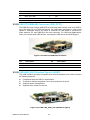
2.3.1 Connector Location
Figure 2.42 RSB-4210 Connector Position (Top)
Figure 2.43 RSB-4210 Connector Position (Bottom)
RSB-4210 User Manual
34
Chapter 2
2.3.2 RSB-4210 Board Dimension
35
RSB-4210 User Manual
H/W Installation
Figure 2.44 RSB-4210 Board Dimension
RSB-4210 User Manual
36
Chapter
3
3
Software Functionality
This chapter details the Linux
operating system on RSB-4210
platform.
The RSB-4210 platform is one embedded system with Windows Embedded Compact
7 (WinEC7). The WinEC7 architecture is a variation of the Windows operating system for minimalistic computers and embedded systems. The preconfigured kernel is
allowed to write applications without creating own operating system kernels. It offers
the possibility to reduce the time to market phase. The purpose of this chapter is to
introduce you how to boot up WinEC7 and some basic utilities on RSB-4210 platform.
3.1 The Bootloader
The main task of the bootloader is to download a WINCE-Image to the platform and
starting WinCE on it. The bootloader can be services to achieve this work through a
terminal running on a host PC. To do so, the host PC has to be connected to the
serial port (UART Port 1) at the platform. There are two kinds of bootloader for RSB4210 WinEC7. One is uboot, and another one is eboot. However, now uboot is the
default bootloader for RSB-4210 WinEC7, eboot is an option bootloader if you want
to use Ethernet KITL at WinEC7 environment.
3.1.1 Communication settings
Please set the host PC's serial port communication and connect to target platform. A
standard serial cable can be used to connect between UART port on the target platform and the development host PC. Any terminal emulation application can be used
to display messages sent from the serial port of the target. Configure the terminal
application with the following communications parameters:
Baudrate
115200 bps
Data bits
8
Stop bits
1
Parity
none
Handshake none
3.1.2 Startup of the bootloader
You can put bootloader (default is uboot) in your favorite boot device including on
board flash (iNand), SD Card, or SATA device. Power on platform will let bootloader
startup, you can press "Enter" to get into uboot command mode as shown in below
figure.
RSB-4210 User Manual
38
Example:
Below is 44 display panel types list table.
Value
Name
Value
Name
Value
Name
0
WUXGA60
15
1440x900RDC
30
720P60
1
UXGA60
16
1440x900P60
31
720P50
2
1080P60
17
WXGA75
32
WSVGA60
3
1080P50
18
WXGA60
33
WSVGA_YING
4
1080I60
19
1366x768P60
34
SVGA85
5
1080I50
20
1366x768CTM
35
SVGA75
6
WSXGA+60
21
1360x768P60
36
SVGA60
7
SXGA+75
22
1280x768P75
37
PAL-TV
8
SXGA+60
23
1280x768RDC
38
NTSC-TV
9
SXGA85
24
1280x768VESA 39
VGA85
10
SXGA75
25
1280x768TV
VGA75
11
SXGA60
26
XGA85
41
VGA72
12
SXGA50
27
XGA75
42
VGA60
13
1280x960P60 28
XGA70
43
720x400P85
14
1440x900P75 29
XGA60
44
640x400P85
255
auto mode
Note!
40
Auto mode: 1280x720 HDMI/1024x768 VGA output, and LVDS output
1280x720 resolution.
39
RSB-4210 User Manual
Software Functionality
RSB-4210 has a build-in CH7033B HDTV/VGA/DVI Encoder. With its advanced
video encoder and flexible scaling engine, the CH7033B satisfies manufactures'
products display requirements. There are 44 display panel types and auto mode can
be chosen as default in RSB-4210. To set default display panel type, just enter uboot
command mode and type below commands:
ch7033cfg set (setting value) : set display panel type
ch7033cfg get : get setting value
reset: reset platform
Chapter 3
3.1.3 Change Display Output Resolution
3.2 WinEC7 Startup Procedure
Windows CE image can be loaded from three devices including SD storage card,
onboard flash chip, and SATA. There is only one device will be the default booting
device. There are two major files that you need to boot WinEC7: u-boot.bin and
NK.nb0. During boot up phase, u-boot will copy WinEC7 image (NK.nb0) to DRAM
and launch it from DRAM from same bootup device. This chapter will introduce you to
how to bootup WinEC7 on RSB-4210 from SD/MMC, on board flash, or SATA device.
Required Files (Please refer to released Software package):
Directory
Files
Note
u-boot.bin
01_First_WinCE
ulogo.bmp
_Boot_No_Hive
NK_VGA_20120621_noHive.nb0
Platform might default be linux. Need
to format on board flash to support
Hive Based WinEC7
02_WinCE_Hive
u-boot.bin
NK.nb0
The latest WinEC7 image and corresponding uboot
03_Cfimager
cfimager.exe
flashSD.bat
eboot.nb0
NK.nb0
NK_VGA_20120621_noHive.nb0
u-boot.bin
Freescale Flash tool to support eboot
and KITL function.
04_Others
--
Other backup files
iMX53_WinEC7_NewArch_bootup_SOP: i.MX53 WinEC7 bootup SOP
Note!
The u-boot in different folder has different functionality, do not use uboot.bin in 01_First_WinCE_Boot_No_Hive folder to boot image in
02_WinCE_Hive folder, vice versa.
RSB-4210 User Manual
40
Please follow bellow steps to boot WinEC7.
1) Platform might default be Linux. Need to format on board flash to support Hive
Based WinEC7.
Insert a boot SD Card to your host pc, and format it to FAT32 Files System.
Chapter 3
3.2.1 WinEC7 Bootup Steps
Software Functionality
Copy 3 files: u-boot.bin, ulogo.bmp, and NK_VGA_20120621_noHive.nb0 from
directory 01_First_WinCE_Boot_No_Hive to your boot SD Card.
Open the Hyperterminal or your telnet program at your working PC.
Setting serial port
41
RSB-4210 User Manual
Insert this bootup SD Card to i.MX53 platform and power on platform.
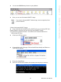
Enter uboot command mode. Set uboot variables >>setenv bootos 'win';
saveenv;
Restart platform, then you can see uboot logo and WinEC7 bootup.
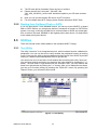
2) Format On Board Flash
Choose the control panel
Choose MMC Card (OnBoardFlash), and create a new partition. Select properties
Dismount -> Format -> Mount
RSB-4210 User Manual
42
Now, you can use Hive-based WinEC7 image.
Note!
If you want to bootup WinEC7 without logo, remove ulogo.bmp from
your boot device.
3) Boot Hive-based WinEC7 image
Copy u-boot.bin and nk.nb0 from 02_WinCE_Hive to your bootup SD Card.
Restart platform, then you can see uboot logo and WinEC7 bootup.
4) If you want to use KITL function. You need to use Freescale flash tool to
flash bootup SD Card.
Check your SD Slot symbol.
Change folder to 03_Cfimager. Edit the flashSD.bat. Modify the SDdevice =
"your SD slot symbol"
Excute the flashSD.bat
User can see the below window. And please press any key to continue
43
RSB-4210 User Manual
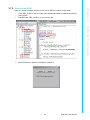
Software Functionality
You can see MMCMemory device on your platform
Chapter 3
The SD card will be formatted. Press any key to continue.
Please check if the "u-boot.bin", "NK.nb0", and
"NK_VGA_20120621_noHive.nb0" had been copied to your SD card successfully.
Now you can use this bootup SD card to try KITL function.
For more detail about KITL usage, please contact Advantech RISC Team.
3.2.2 Booting form On Board Flash or SATA
If you can boot WinEC7 from SD/MMC device, you can try to boot WinEC7 on board
flash or SATA. Before you using these devices, remember to format it to FAT32 files
system. Just copy u-boot.bin and NK.nb0 to on board flash or SATA and restart platform to achieve this task. SD/MMC is the highest priority boot device. On board flash
is the lowest priority boot device.
3.3 Utilities
There are several useful utilities added in the released WinEC7 image.
3.3.1 Test Utility
The utility "Auto.exe" is an integrated test tool, which includes function validation for
peripherals. You can use this tool to verify whether the peripheral function is working
or not. Just copy this utility to storage device and then launch from WinCE by double
clicking it. Please contact Adavantech FAEs to get this tool.
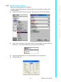
You should see a lot of test items in left window after launching this utility "Auto.exe".
You can insert enough test items you want into the right window by pressing the ">>"
button. The test items in right window will be executed. Also, you can remove test
items from right window by clicking the "<<" button. After you've added the test items,
you can go to function testing by pressing the "RUN ALL" button. By pressing the
"Report" button, you will see the test results.
Figure 3.1 Test Utility
RSB-4210 User Manual
44
The RSB-4210 platform has a useful function called "Startup execution". After the
system boot up, the startup execution function would automatically perform. This
function is useful for controlling the system to do the initialization processes or some
other procedures. In RSB-4210 platform, follow below method to perform the
"Startup" function.
Example:
Copy executable files "AdvRebootCounter.exe" in "\SD Memory\Startup", and then
reboot the system. After the system boots up, the executable files would automatically execute.
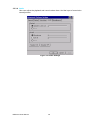
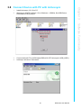
3.3.3 Platform Setting
The Platform Setting utility is an outstanding utility designed by Advantech Windows® CE software team. It is an integrated environment where users can get useful
system information as well as configure favorite system settings and apply system
control functions on demand. The Platform Setting icon is on the desktop. The following sections illustrate the functions of Platform Setting.
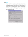
3.3.3.1 General
'General' page shows the memory information including DRAM and iNAND. Platform
name and System Software version are also in here.
Figure 3.2 General Information
45
RSB-4210 User Manual
Software Functionality
Method:
Step 1. Create a folder named "Startup" in a storage media (onboard flash or SD storage card).
Step 2. Copy executable files to "Startup" folder that is created by Step 1.
Chapter 3
3.3.2 Startup Execution
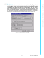
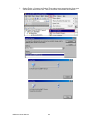
3.3.3.2 Display
From time to time it is unnecessary to turn on the display attached to the RSB-4210
all day long. The Display page provides several frequently used functions such as
turning off the LCD and backlight to elongate the display repair period, adjusting
brightness. Furthermore, users can click the "Turn Off" button to turn off the backlight
of the display panel immediately without waiting. Once the backlight is off, there are
three inputs to turn it on: (1) mouse; (2) keyboard; (3) touch-screen; users can use
any one of them to turn on the display. The lower "Brightness" block has scroll bars
by which users can fine tune the brightness levels of the LCD. You can also change
resolution by selecting VGA group check button. However, this feature is only for
Hive-based image and you need to restart platform to change resolution. To customize your own resolution, you need get Binary BSP from Advantech FAEs. The default
custom resolution is 800x600 now.
Figure 3.3 Display Configuration
RSB-4210 User Manual
46
47
RSB-4210 User Manual
Software Functionality
Figure 3.4 Watchdog Timer
Chapter 3
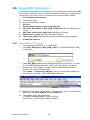
3.3.3.3 WatchDog Timer
It is important in industrial applications that control systems rarely crash, or are capable of self-resetting if they hang or stop functioning. The Watchdog function for automatic system resetting is therefore provided in RSB-4210. There is a timer inside the
watchdog function. User's AP could invoke the associated APIs in the Watchdog
function to start the timer, then the Watchdog function would repeat the countdown of
the specified period of time to reboot the system if the user's AP does not clear the
timer in time periodically. The Watchdog function in the RSB-4210 provides eight different time intervals: 1 second, 5 seconds, 10 seconds, 15 seconds, 20 second, 25
seconds, and 30 seconds. The "Enable" button is used to start the Watchdog function. Pressing the "Sleep" button will cause the system into suspend mode. Pressing
the "ReBoot" button will cause the system to cold boot.
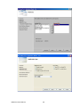
3.3.3.4 Audio
User can adjust the playback and record volume here. And the input of record also
can adjust here.
Figure 3.5 Audio Settings
RSB-4210 User Manual
48
Chapter 3
3.3.3.5 Miscellaneous
The Misc page provides several functions as described below. The "Registry" block
provides registry save and registry clean functions. Pressing the "Save" button, the
registry settings will be saved to persistent storage as on-board flash. Pressing
"Clean" button, the registry setting will return to default settings. The "Start Service"
button invokes ActiveSync to the host computer. The "Ethernet Information" block
shows the network MAC address. The Memory Management block will check if memory size needs to be allocated automatically during boot. Once this is checked, program memory will be allocated half, and storage memory will occupy the rest.
Software Functionality
Figure 3.6 Miscellaneous Settings
49
RSB-4210 User Manual
3.4 Network
RSB-4210 has two builds in 10/100Base-T Ethernet controller. It appears at "Control
Panel/Network and Dial-up Connections". User can configure its Ethernet support as
follows:
1. Click "Start/Settings/Control Panel".
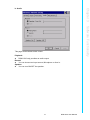
2. Double click "Network and Dial-up Connections".
3. If the RSB-4210 is a node of the LAN with DHCP servers, it is now available.
3.9.3. If the RSB-4210 is a node of the LAN with fixed IP, the user has to consult with
MIS to get specific IP addresses. Then fill them into the associated fields of the Properties Dialog, then press the registry save button to save this changed registry.
Reboot the system, and the Ethernet functions would be available as the previous
configuration.
Figure 3.7 Networking via Ethernet
3.5 BSP Carried Tools
The Freescale board support package (BSP) is based on the Microsoft Windows
Embedded Compact 7 operating system. It has some build-in tools to verify WinEC7
functionality and BSP's drivers. This section will introduce these tools.
3.5.1 Display and Video Testing Tools
The Windows Embedded Compact 7 BSP display driver is based on the Microsoft
DirectDraw Graphics Primitive Engine (DDGPE) classes and supports the Microsoft
DirectDraw interface. This driver combines the functionality of a standard LCD display with DirectDraw support.
RSB-4210 User Manual
50
51
RSB-4210 User Manual
Software Functionality
Figure 3.8 Display Driver GUI
Chapter 3
3.5.1.1 Using The Display Driver Control Panel Application
A control panel application provides access to additional display driver functionality.
Look for the icon shown in Figure 3.8 in Windows CE control panel.
The control panel application supports the following display driver features:
Rotation between 0°, 90°, 180°, and 270°.
Gamma correction configuration for a synchronous display device, The gamma
value may be set between 0.5 and 3.5. The default gamma value is 1.0.
Display mode configuration with a drop-down box listing all of the display modes
supported by the display driver. Each display mode is listed as a combination of
the mode width, height, and frequency. For example, 800×480@60Hz represents the WVGA panel LCD mode, and 720×480@50Hz represents NTSC TV
mode. The resolution of the current mode is displayed in the box. However, you
can't change resolution when kernel running. This application is located
under \Startup\Settings\Control Panel\Freescale display driver.
3.5.1.2 Running the PlayWnd tests
For PlayWnd testing, there are no build steps required. playwnd.exe always is
included in the image. This sample is an interactive audio/video media file player. It
uses DirectShow to play any supported audio or video media file (MPG, AVI, QT,
WAV, AU, SND, MID, etc.). The video will appear in a window on the screen, and you
can use a mouse to move the window. If the media has a video component, PlayWnd
will read the video's default size and adjust the player's client area to allow the video
to play at its exact default size (taking into account the size of caption bar & borders).
When the media file is playing, the menu bar will disappear, giving you keyboard control with 'P' and 'S' for pause/play and stop/reset. This application is located under
\Windows\ PlayWnd.exe.
RSB-4210 User Manual
52
If both the SGTL5000 stereo audio driver and the SPDIF driver occur, the default
audio device may be SGTL5000. The default audio device can be chosen by the
AudioRouting application. Now SGTL5000 support input and output, and SPDIF only
support output. This application is located under \Windows\ AudioRouting.exe.
Chapter 3
3.5.2 AudioRouting
Software Functionality
3.5.3 Graphics Processing Unit Testing Tools
The Graphics Processing Unit (GPU) is a graphics accelerator targeting embedded
2D/3D graphics applications. The GPU3D (3D graphics processing unit) is based on
the AMD Z430 core, which is an embedded engine capable of DirectX9 Shader
Model 3.0+ program execution and accelerates user level graphics APIs such as
OpenGL ES 1.1 and 2.0.. The GPU2D (2D graphics processing unit) is based on the
AMD Z160 core, which is an embedded 2D and vector graphics accelerator targeting
the OpenVG 1.1 graphics API and feature set The GPU driver is delivered only as
binary code.
53
RSB-4210 User Manual
3.5.3.1 Tiger Test
This test application verifies the basic functionality of OpengVG 1.1. It is included into
the release image and is located under \Windows\tiger.exe. Click to launch this test
and a rotating tiger appears on the screen as shown in follow figure.
Figure 3.9 Tiger Test
3.5.3.2 Cube Test
This test application verifies the basic functionality of OpengGL ES 1.1. It is included
in the release image and is located under \Windows\cube.exe. Click to launch this
test and a rotating cube appears on the screen as shown in follow figure. Press ESC
to exit this application.
Figure 3.10 Cube Test
RSB-4210 User Manual
54
3.5.4 Application Tool for USB Device Class Select
There are three types of USB device classes: ActiveSync, MSC and RNDIS. An
application with a GUI is provided to switch between the three classes. Figure X
shows the tool to switch the USB device class. Make sure the OTG port is operating
under the USB device mode (by connecting the mini-B connector of the USB OTG
cable to the OTG port in the board) before pressing the Apply button to switch USB
device class.
Figure 3.12 USB Device Class Switch User Interface
55
RSB-4210 User Manual
Software Functionality
Figure 3.11 Triangle Test
Chapter 3
3.5.3.3 Triangle Test
This test application verifies the basic functionality of OpengGL ES 2.0. It is included
in the release image and is located under \Windows\triangle.exe. Click to launch this
test and a triangle appears on the screen as shown in follow figure. Press ESC to exit
this application.
3.6 Binary BSP introduction
The purpose of this section is to show you how to use Advantech WinCE Binary BSP
to develop your WinCE system for i.MX53 series platform. Before you begin this document's step, you need to check a development environment listed as below:
1. PC development environment.
Visual Studio 2008
Windows Embedded Compact 7
2. SD Card.
3. Released BSP package contains following files:
ADV_RSB_4210.pbxml (or ADV_ROM_1210.pbxml): WinCE OSDesing Project file.
ADV_RSB_4210(or ADV_ROM_1210): BSP Binary Package.
RSB_4210xx_x_(date)_S: Image and bootup package
uboot_logo_(date): uboot source code and programming guide package.
4. A RSB-4210 Platform.
3.6.1 Build WinEC7 OS Image
1.
2.
Assume default WinCE path is "C:\WINCE700".
Copy ADV_RSB_4210 (or ADV_ROM_1210) to "C:\WINCE700\PLATFORM",
for example
3.
Place ADV_ROM_1210.pbxml to OSDesigns\[create a sub-folder]\ , for example: C:\WINCE700\osdesigns\ADV_ROM_1210\ ADV_ROM_1210.pbxml
Double Click "ADV_ROM_1210.pbxml". Start a VS2008 WinCE Platform
Builder. It will create OSDesigns files.
Select Build -> Configuration Manager from your Visual Studio 2008 menu
bar. Choose "Freescale i_MX53 SMD ARMV7 Release"
4.
5.
Make Run-Time Image: Select Build -> Build Solution from your Visual Studio
2008 menu bar. Never Rebuild, or Clean solution !!
The WinEC7 image will be placed at
"C:\WINCE700\osdesigns\ADV_ROM_1210\RelDir\Freescale_i_MX53_SMD_ARMV7_Release"
RSB-4210 User Manual
56
Please refer to Section 3.2. Copy the compiled NK.nb0 image to your boot device.
Follow Section 3.2 to boot up your platform.
3.6.3 U-boot development
Please refer to RSB-4210 Linux Eva-kit user manual and winec7-uboot-programingguide_(date) to develop u-boot if you want to customize it.
The purpose of this document is to introduce the method of remote debug a Visual
C++ program of Windows Embedded Compact 7 (Windows EC7) Smart Device by
using Activesync utility connection. Before you begin this document's step, you need
to setup a development environment listed as below:
1. Visual Studio 2008 development environment on your Desktop PC.
(Visual Studio 2008 SP1)
2. Install target device SDK
(For example, ROM-1210.msi for RSB-4210 platform)
3. Windows Embedded Compact 7.0 device.
3.7.1 Create a new Windows EC 7 project
1.
2.
3.
4.
5.
6.
Select File -> New -> Project... from your Visual Studio 2008 menu bar.
Select Project Types: Smart Device of Visual C++.
Select Visual Studio Installed Templates: MFC Smart Device Application.
Type "Project Name"
Select Target platform SDK: ROM-1210.
Base on your application to choice Application Type, EX:"Dialog Based".
57
RSB-4210 User Manual
Software Functionality
3.7 SDK introduction
Chapter 3
3.6.2 Windows CE Startup Procedure
RSB-4210 User Manual
58
Here is a simple example show you how to use SUSI to control buzzer beep.
1. Copy REL_SUSI.H, and susi.lib to your application folder and add these files to
your project.
2. Add #include "REL_SUSI.H" to your source file.
Chapter 3
3.7.2 How to use SUSI
Software Functionality
3.
Draw 2 buttons in previous example in Section 2.
59
RSB-4210 User Manual
4.
Add following code to enable SUSI init
5.
Add following code to control buzzer
6.
7.
Then you can Start Debugging with ActiveSync to try SUSI API.
Other SUSI API please refer to RSB-4210-SUSI_User_Maunal document.
RSB-4210 User Manual
60
Install Activesync 3.9.3.5 on PC
Startup your WinEC7 platform. Go to Windows -> USBSet, Set USB Device
Class Select to Active Sync.
3.
4.
Connect device & PC via USB cable (RSB-4210 OTG client port is USB_ORG1)
Activesync will show "Connected"
Software Functionality
1.
2.
Chapter 3
3.8 Connect Device with PC with Activesync
61
RSB-4210 User Manual
5.
Select Tools -> Connect to Device (Then select your target device) from your
Visual Studio 2008 menu bar. Then it will show "Connection succeeded"
RSB-4210 User Manual
62
1.
2.
3.
4.
5.
Set breakpoints at you code, for example, code linesCfsl_tset_20110805Dlg::OnBnClickedButton26; SusiCoreSetBuzzer(1);
Then press "F5' to Start Debugging
Then you can see that it will stop at the breakpoint you set.
Then press "F5' to Continues Debugging, it will go to next breakpoint you set.
Finally, you can see you AP shown at the LCD screen of device
Chapter 3
3.9 Implement Break Points
Software Functionality
63
RSB-4210 User Manual
3.10 SUSI Library
SUSI - A Bridge to Simplify & Enhance H/W & Application Implementation Efficiency
When developers want to write an application that involves hardware access, they
have to study the specifications to write the drivers. This is a time-consuming job and
requires lots of expertise.
Advantech has done all the hard work for our customers with the release of a suite of
APIs (Application Programming Interfaces), called the Secured & Unified Smart Interface (SUSI).
SUSI provides not only the underlying drivers required but also a rich set of userfriendly, intelligent and integrated interfaces, which speeds development, enhances
security and offers add-on value for Advantech platforms. SUSI plays the role of catalyst between developer and solution, and makes Advantech embedded platforms
easier and simpler to adopt and operate with customer applications.
RSB-4210 User Manual
64
SUSI Contains 5 + 1 Categories of Features:
Control
Control the devices connected to GPIO and I2C.
Display
Adjust the brightness of LCD panels or turn on/off the power of display devices.
Monitor
Monitor the system status, including voltage, temperature, fan speed and
Watchdog function to restart if the system freezes or crashes.
Power Saving
Power Saving utility and API for software developers.
Security
API for AES encryption, RNG (random number generator), SRAM mirror feature
and security ID storage.
Debug
Easier debugging with SUSI; when a SUSI API call fails, error codes help programmers know what exactly the error is. All the possible errors have been
listed.
SUSI-RISC supports Control, Display and Monitor functions.
Control
– GPIO
General Purpose Input/Output is a flexible parallel interface that allows a variety of custom connections. It supports various Digital I/O devices - input
devices like buttons, switches; output devices such as cash drawers, LED
lights etc. And, allows users to monitor the level of signal input or set the output status to switch on/off the device.
65
RSB-4210 User Manual
Software Functionality
Faster Time to Market
SUSI's unified API helps developers write applications to control the hardware
without knowing the hardware specs of the chipsets and driver architecture.
Reduced Project Effort
When customers have their own devices connected to the onboard bus, they
can either: study the data sheet and write the driver & API from scratch, or they
can use SUSI to start the integration with a 50% head start. Developers can reference the sample program on the CD to see and learn more about the software
development environment.
Enhances Hardware Platform Reliability
SUSI provides a trusted custom ready solution which combines chipset and
library function support, controlling application development through SUSI
enhances reliability and brings peace of mind.
Flexible Upgrade Possibilities
SUSI supports an easy upgrade solution for customers. Customers just need to
install the new version SUSI that supports the new functions.
Chapter 3
Benefits
– Programmable GPIO
The Programmable GPIO API allows developers to dynamically set the GPIO
input or output status, GPIO in/out status is usually defined in BIOS, if customers need to have different settings, they must modify the BIOS. Now with
the new Programmable GPIO, customers can change the settings in their
application by calling the SUSI API; greatly saving development time.
– I2C
I2C is a bi-directional two wire bus that was developed by Philips for use in
their televisions in the 1980s. Today, I2C is used in all types of embedded
systems. The I2C API allows a developer to interface a CE PC to a downstream embedded system environment and transfer serial messages using
the I2C protocols, allowing multiple simultaneous device control.
Monitor
– Watchdog
A watchdog timer (WDT) is a device or electronic card that performs a specific operation after a certain period of time if something goes wrong with an
electronic system and the system does not recover on its own.
A watchdog timer can be programmed to perform a warm boot (restarting the
system) after a certain number of seconds during which a program or computer fails to respond following the most recent mouse click or keyboard
action.
Display
– Brightness Control
The Brightness Control API allows a developer to interface Windows CE PC
to easily control brightness.
RSB-4210 User Manual
66
The Backlight API allows a developer to control the backlight (screen) on/off
in Windows CE.
SUSI-RISC currently supports one OS - Windows CE. Contents are listed below:
Operating System
Windows CE
Directory
User Manual
Location
Installation
\Program Files\SUSI\V30
Image Built-in *
Contents
SUSI_User_Manual.pdf
Susi.lib
Function export
Library Files
Susi.dll
Dynamic link library
Include Files
Susi.h
ioctrl.h / REL_SUSI.h
AdvPlatformSetting.exe
SusiDemo
Demo program execution file
Susi.dll
Dynamic link library
SusiDemo\SRC\ C
Source code of SusiDemo program in EVC
* Windows CE manual installation:
You can add the SUSI Library into the image by editing any bib file. First you open
project.bib in the platform builder. Add this line to the MODULES section of project.bib Susi.dll $(_FLATRELEASEDIR)\Susi.dll NK SH
If you want to run the window-based demo, add the following line: AdvPlatformSetting.exe $(_FLATRELEASEDIR)\ AdvPlatformSetting.exe
Place the three files into any files directory.
Build your new Windows CE operating system.
67
RSB-4210 User Manual
Software Functionality
3.10.1 Package Contents
Chapter 3
– Backlight
3.10.2 Additional Programs
3.10.2.1 Demo Program
The SUSI demo program demonstrates how to incorporate SUSI library into the
user's own applications. The program is written in EVC programming language and
based on Windows Embedded Compact 7.
3.10.2.2 AdvPlatformSetting.exe
The execution file, AdvPlatformSetting.exe, released with source code can be run on
Windows EC7.
The following pages are a detailed introduction to the AdvPlatformSetting program:
i. General
Figure 3.13 General Information
All platform information is showed in this page.
Platform Information
Show H/W platform information.
Memory Size
Show memory information.
Show NAND Flash information
System Software
Show information about the Operating System
Show information about Boot Loader.
Show information about platform.
RSB-4210 User Manual
68
Chapter 3
ii. Display
69
RSB-4210 User Manual
Software Functionality
This page is about VGA control. You can control Backlight, Brightness and Screen
resolution. ROM-1210 does not support to adjust contrast.
Backlight:
Turn ON/OFF backlight.
Brightness:
Change the brightness from 0 up to 255.
VGA:
Change screen resolution.
iii. Watchdog
This page contains "Watchdog" and "Power Management".
Watchdog Timer:
A configurable time out counter with Time-out periods from 0.5 seconds up to
128 seconds.
Time resolution of 0.5 seconds.
Before the timer counts down, you may reset the timer by clicking the "Trigger"
button. "Stop" function is not supported in SUSI-RISC.
Power Management:
This part implements Sleep function and Reboot function.
RSB-4210 User Manual
70
Chapter 3
iv. Audio
Software Functionality
This page demonstrates audio control.
Playback:
ROM-1210 only provides an audio output.
Record:
You can choose two input source, Microphone or Line In.
Speaker:
You can turn ON/OFF the speaker.
71
RSB-4210 User Manual
v. Miscellaneous
Miscellaneous page contains Registry Control, ActiveSync, Ethernet Information and
Touch Panel Calibrate.
Registry:
Our BSP supports hive-based registry. With the hive-based registry, you may
save the changes in files on a storage device. For performance reasons, the
registry changes saved after you had called "RegFlushKey".
ActiveSync:
ActiveSync allows you to transfers files from your PC to the Windows Mobile
platform, and opens up a gateway to synchronizing data from your phone with
your desktop computer.
Ethernet Information:
This part shows MAC Address of Ethernet chipset.
Touch Panel:
You can calibrate the touch screen.
RSB-4210 User Manual
72
3.10.2.3 Programming Overview
Header Files
SUSI.H includes API declaration, constants and flags that are required for programming.
DEBUG.H / ERRDRV.H / ERRLIB.H are for debug code definitions.
DEBUG.H - Function index codes
ERRLIB.H - Library error codes ERRDRV.H - Driver error codes
Chapter 3
Library Files
Susi.lib is for library import and Susi.dll is a dynamic link library that exports all the
API functions.
Software Functionality
Installation File
In Windows CE, the files and drivers mentioned above are already built-in to the
image.
Dll functions
SusiDll- APIs are driver-independent, i.e. they can be called without any drivers. In
Windows CE, after drivers having been installed, users have to call SusiDllInit for initialization before using any other APIs that are not SusiDll-prefixed. Before the application terminates, call SusiDllUnInit to free allocated system resources.
When an API call fails, use SusGetLastError to get an error report. An error value will
be either
Function Index Code + Library Error Code, or
Function Index Code + Driver Error Code
The Function Index Code indicates which API the error came from and the library /
Driver Error Code indicates the actual error type, i.e. whether it was an error in a
library or driver. For a complete list of error codes, please refer to the Appendix.
Core functions
SusiCore- APIs are available for all Advantech SUSI-enabled platforms to provide
board information such as the platform name and BIOS version. New
SusiCoreAccessBootCounter and SusiCoreAccessBootCounter APIs are Boot Logger features that enable monitoring of system reboot times, total OS run time and
continual run time.
Watchdog (WD) functions
The hardware watchdog timer is a common feature among all Advantech platforms.
In user applications, call SusiWDSetConfig with specific timeout values to start the
watchdog timer countdown, meanwhile create a thread or timer to periodically refresh
the timer with SusiWDTrigger before it expires. If the application ever hangs, it will fail
to refresh the timer and the watchdog reset will cause a system reboot.
73
RSB-4210 User Manual
GPIO (IO) functions
There are two sets of GPIO functions. It is highly recommended to use the new one.
With pin read and write, more flexibility has been added to allow easy pin direction
change as needed, as well as the capability of reading output pin status.
GPIO function set:
Refer to Appendix for pin allocation and their default direction.
IIC functions
The APIs here cover IIC standard mode operations with a 7-bit device address:
The slave address is expressed as a 7-bit hex number between 0x00 to 0x7F, however the actual addresses used for R/W are 8?bit write address = 7?bit address <<1
(left shift one) with LSB 0 (for write)
8-bit read address = 7-bit address <<1 (left shift one) with LSB 1 (for read)
E.g. Given a 7-bit slave address 0x20, the write address is 0x40 and the read
address is 0x41.
Here in all APIs, parameter SlaveAddress is the 8-bit address and users don't need
to care about giving it as a read or write address, since the actual R/W is taken care
by the API itself, i.e. you could even use a write address, say 0x41 for APIs with write
operation and get the right result, and vice versa.
For more details on platform IIC/SMBus support, please refer to Appendix A.
VGA Control (VC) functions
SusiVC- functions support VGA signal ON/OFF on all SUSI-enabled platforms and
also LCD brightness adjustment. One application of SusiVCScreenOn and SusiVCScreenOff is to have the display signal disabled when system idles after certain
period of time to expand the panel life span.
RSB-4210 User Manual
74
All APIs return the BOOL data type except Susi*Available and some special cases
that are of type int. If any function call fails, i.e. a BOOL value of FALSE, or an int
value of -1, the error code can always be retrieved by an immediate call to SusiGetLastError.
3.10.3.1 SusiDllInit
Initialize the Susi Library.
BOOL SusiDllInit(void)
Return Value
TRUE (1) indicates success; FALSE (0) indicates failure.
Remarks
An application must call SusiDllInit before calling any other non SusiDll functions.
3.10.3.2 SusiDllUnInit
Unload the Susi Library.
BOOL SusiDllUnInit(void)
Parameters
None.
Return Value
TRUE (1) indicates success; FALSE (0) indicates failure.
Remarks
Before an application terminates, it must call SusiDllUnInit if it has successfully called
SusiDllInit. Calls to SusiDllInit and SusiDllUnInit can be nested but must be paired.
75
RSB-4210 User Manual
Software Functionality
Parameters
None.
Chapter 3
3.10.3 SUSI API Programmer's Documentation
3.10.3.3 SusiDllGetVersion
Retrieve the version numbers of SUSI Library.
void SusiDllGetVersion(WORD *major, WORD *minor)
Parameters
major
[out] Pointer to a variable containing the major version number.
minor
[out] Pointer to a variable containing the minor version number.
Return Value
None.
Remarks
This function returns the version numbers of SUSI. It's suggested to call this function
first and compare the numbers with the constants SUSI_LIB_VER_MJ and
SUSI_LIB_VER_MR in header file SUSI.H to ensure the library compatibility.
3.10.3.4 SusiDllGetLastError
This function returns the last error code value.
int SusiDllGetLastError(void)
Parameters
None.
Return Value
The code of error reason for the last function call with failure.
Remarks
You should call the SusiDllGetLastError immediately when a function's return value
indicates failure.
The return error code will be either
Function Index Code + Library Error Code, or
Function Index Code + Driver Error Code
The Function Index Code distinguishes which API the error resulted from and the
library / Driver Error Code indicates the actual error type, i.e. if it is an error in a library
or driver. For a complete list of error codes, please refer to the Appendix.
RSB-4210 User Manual
76
Chapter 3
3.10.3.5 SusiCoreAvailable
Check if Core driver is available.
int SusiCoreAvailable (void)
Parameters
None.
Value
-1
0
1
Meaning
The function fails.
The function succeeds; the platform does not support
SusiCore- APIs.
The function succeeds; the platform supports Core.
Remarks
After calling SusiDllInit successfully, all Susi*Available functions are used to check if
the corresponding features are supported by the platform or not. So it is suggested to
call Susi*Available before using any Susi*- functions.
3.10.3.6 SusiCoreGetPlatformName
Get the current platform name.
BOOL SusiCoreGetPlatformName(TCHAR *PlatformName, DWORD
*size)
Parameters
PlatformName
[out] Pointer to an array in which the platform name string is returned.
size
[in/out] Pointer to a variable that specifies the size, in TCHAR, of the array
pointed to by the PlatformName parameter.
If PlatformName is given as NULL, when the function returns, the variable
will contain the array size required for the platform name.
Return Value
TRUE (1) indicates success; FALSE (0) indicates failure.
Remarks
Call the function twice, first by giving PlatformName as NULL to get the array size
required for the string. Then allocate a TCHAR array with the size required and give
the array with its size as parameters to get the platform name. Note that the platform
name cannot be correctly retrieved if the BIOS is a release version.
77
RSB-4210 User Manual
Software Functionality
Return Value
3.10.3.7 SusiCoreSoftReset
Software reset function.
BOOL SusiCoreSoftReset(void)
Parameters
None.
Return Value
TRUE(1) indicates success; FALSE(0) indicates failure.
Remarks
Call this function to do software reset.
3.10.3.8 SusiCoreGetImageInfo
Get image information, including WinCE image version, WinCE image build date,
Boot loader image version, and Boot loader image build date.
BOOL SusiCoreGetImageinfo(PIMGINFO pInfo)
Paramete
pInfo
[out] Retrieve image information
ImageInfo structure definition :
typedef struct {
TCHAR
*WinCEImageVersion;
TCHAR
*WinCEBuiltDate;
TCHAR
*BootloaderVersion;
TCHAR
*BootloaderDate;
} PIMGINFO, *PIMGINFO
Return Value
TRUE(1) indicates success; FALSE(0) indicates failure.
Remarks
Programmer can adjust program memory size in Mbytes by using this function. The
format of WinCEBuiltDate & BootloaderDate is yyyymmdd.
RSB-4210 User Manual
78
Parameters
MACAddr
[out] Pointer to a byte array containing the MAC address of LAN chip.
Software Functionality
Return Value
TRUE(1) indicates success; FALSE(0) indicates failure.
3.10.3.10SusiCoreSetMACAddr
Set MAC Address of LAN chip.
BOOL SusiCoreSetMACAddr (BYTE *MACAddr)
Parameters
MACAddr
[in] Pointer to a byte array which is the new MAC address.
Return Value
TRUE(1) indicates success; FALSE(0) indicates failure.
3.10.3.11SusiCoreRegistrySave
Save registry.
BOOL SusiCoreRegistrySave(void)
Parameters
None.
Return Value
TRUE(1) indicates success; FALSE(0) indicates failure.
Remarks
Call this function to save registry.
79
Chapter 3
3.10.3.9 SusiCoreGetMACAddr
Get MAC Address of LAN chip.
BOOL SusiCoreGetMACAddr (BYTE *MACAddr)
RSB-4210 User Manual
3.10.3.12SusiCoreRegistryClean
Clean registry to default.
BOOL SusiCoreRegistryClean(void)
Parameters
None.
Return Value
TRUE(1) indicates success; FALSE(0) indicates failure.
Remarks
Call this function to clean registry to default value, and then reset platform.
3.10.3.13SusiWDGetRange
Get the step, minimum and maximum values of the watchdog timer.
BOOL SusiWDGetRange(DWORD *minimum, DWORD
DWORD *stepping)
*maximum,
Parameters
Minimum
[out] Pointer to a variable containing the minimum timeout value in
milliseconds
Maximum
[out] Pointer to a variable containing the maximum timeout value in
milliseconds
Stepping
[out] Pointer to a variable containing the stepping timeout value in
milliseconds
Return Value
TRUE (1) indicates success; FALSE (0) indicates failure.
Remarks
The values may vary from platform to platform; depending on the hardware implementation of the watchdog timer. For example, if the minimum timeout is 1000, the
maximum timeout is 63000, and the step is 1000, it means the watchdog timeout will
count 1, 2, 3 … 63 seconds.
RSB-4210 User Manual
80
Return Value
TRUE (1) indicates success; FALSE (0) indicates failure
Remarks
Once the watchdog has been activated, its timer begins to count down. The application has to periodically call SusiWDTrigger to refresh the timer before it expires, i.e.
reload the watchdog timer within the specified timeout or the system will reboot when
it counts down to 0.
Actually a subsequent call to SusiWDTrigger equals a call to SusiWDSetConfig with
delay 0 and the original timeout value, so if you want to change the timeout value, call
SusiWDSetConfig with new timeout value instead of SusiWDTrigger.
Use SusiWDGetRange to get the acceptable timeout values.
3.10.3.15SusiWDTrigger
Reload the watchdog timer to the timeout value given in SusiWDSetConfig to prevent
the system from rebooting.
BOOL SusiWDTrigger(void)
Parameters
None.
Return Value
TRUE (1) indicates success; FALSE (0) indicates failure.
Remarks
A watchdog protected application has to call SusiWDTrigger continuously to indicate
that it is still working properly and prevent a system restart. The first call to SusiWDTrigger in the middle of a delay resulting from a previous call to SusiWDSetConfig
causes the delay timer to be canceled immediately and starts the watchdog timer
countdown from the timeout value. It is always a good choice for users to have a longer delay time in SusiWDSetConfig.
81
RSB-4210 User Manual
Software Functionality
Parameters
delay
[in] Specifies a value in milliseconds which will be added to "the first" timeout
period. This allows the application to have sufficient time to do initialization
before the first call to SusiWDTrigger and still be protected by the watchdog.
timeout
[in] Specifies a duration in milliseconds for the watchdog timeout.
Chapter 3
3.10.3.14SusiWDSetConfig
Start watchdog timer with specified timeout value.
BOOL SusiWDSetConfig(DWORD delay, DWORD timeout)
3.10.3.16SusiIOAvailable
Check if GPIO driver is available.
int SusiCoreAvailable (void)
Parameters
None.
Return Value
Value
-1
0
1
Meaning
The function fails.
The function succeeds; the platform does not support
SusiIO- APIs.
The function succeeds; the platform supports GPIO.
Remarks
After calling SusiDllInit successfully, all Susi*Available functions are used to check if
the corresponding features are supported by the platform or not. It is suggested to
call Susi*Available before using any Susi*- functions.
RSB-4210 User Manual
82
Query the current number of input and output pins.
BOOL SusiIOCountEx(DWORD *inCount, DWORD *outCount)
Return Value
TRUE (1) indicates success; FALSE (0) indicates failure.
Remarks
The number of GPIO pins equals the number of input pins plus the number of output
pins. The number of input and output pins may vary in accordance with the current
pin direction.
3.10.3.18SusiIOSetDirection
Set direction of one GPIO pin as input or output.
BOOL SusiIOSetDirection(BYTE PinNum,
DirMask)
BYTE
IO,
DWORD *Pin-
Parameters
PinNum
[in] Specifies the GPIO pin to be changed, ranging from 0 ~ (total number of
GPIO pins minus 1).
IO
[in] Specifies the pin direction to be set.
PinDirMask
[out] Pointer to a variable in which the function returns the latest direction
mask after the pin direction is set.
Return Value
TRUE (1) indicates success; FALSE (0) indicates failure.
Remarks
Use an IO value of 1 to set a pin as an input or 0 to set a pin as an output.
The function can only set the direction of one of the pins that are direction configurable. If the pin number specified is an invalid pin or a pin that can only be configured
as an input, the function call will fail and return FALSE.
83
RSB-4210 User Manual
Software Functionality
Parameters
inCount
[out] Pointer to a variable in which this function returns the count of
input pins.
outCount
[out] Pointer to a variable in which this function returns the count of
output pins.
Chapter 3
3.10.3.17SusiIOCountEx
3.10.3.19SusiIOReadEx
Read current status of one GPIO input or output pin.
BOOL SusiIOReadEx(BYTE PinNum, BOOL *status)
Parameters
PinNum
[in] Specifies the GPIO pin demanded to be read, ranging from 0 ~ (total
number of GPIO pins minus 1).
status
[out] Pointer to a variable in which the pin status returns.
Return Value
TRUE (1) indicates success; FALSE (0) indicates failure.
Remarks
If the pin is in status high, the value got in status will be 1. If the pin is in status low, it
will be zero. The function is capable of reading the status of either an input pin or an
output pin.
3.10.3.20SusiIOWriteEx
Set one GPIO output pin as status high or low.
BOOL SusiIOWriteEx(BYTE PinNum, BOOL status)
Parameters
PinNum
[in] Specifies the GPIO pin demanded to be written, ranging from 0 ~ (total
number of GPIO pins minus 1).
status
[in]Specifies the GPIO status to be written.
Return Value
TRUE (1) indicates success; FALSE (0) indicates failure.
Remarks
The function can only set the status of one of the output pins. If the pin number specified is an input pin or an invalid pin, the function call will fail and return with FALSE. A
status with 1 to set the pin as output high, 0 to set the pin as output low.
RSB-4210 User Manual
84
Parameters
None.
Chapter 3
3.10.3.21SusiIICAvailable
Check if I2C driver is available and also get the IIC type supported.
int SusiIICAvailable()
Return Value
0
SUSI_IIC_TYPE_PRIMARY (1)
SUSI_IIC_TYPE_SMBUS (2)
SUSI_IIC_TYPE_BOTH (3)
Meaning
The function fails.
The function succeeds; the platform does not
support any SusiIIC - APIs.
The function succeeds; the platform supports
only primary IIC.
The function succeeds; the platform supports
only SMBus implemented IIC.
The function succeeds; the platform supports
both primary IIC and SMBus IIC.
Remarks
After calling SusiDllInit successfully, all Susi*Available functions are use to check if
the corresponding features are supported by the platform or not. So it is suggested to
call Susi*Available before using any Susi*- functions.
85
RSB-4210 User Manual
Software Functionality
Value
-1
3.10.3.22SusiIICRead
Read bytes of data from the target slave device in the I2C bus.
SUSI_API BOOL SusiIICRead(DWORD IICType, BYTE SlaveAddress,
BYTE *RegInx, BYTE *ReadBuf, DWORD ReadLen)
Parameters
IICType
[in]Specifies that I2C type, the value can either be
SUSI_IIC_TYPE_PRIMARY (1)
SUSI_IIC_TYPE_SMBUS (2)
SlaveAddress
[in] Specifies the 8-bit device address, ranging from 0x00 - 0xFF.
Whether to give a 1 (read) or 0 (write) to the LSB of SlaveAddress could
be ignored.
RegInx
[in] Registry Index.
ReadBuf
[out] Pointer to a variable in which the function reads the bytes of data.
ReadLen
[in] Specifies the number of bytes to be read.
Return Value
TRUE (1) indicates success; FALSE (0) indicates failure.
Remarks
Call SusiIICAvailable first to make sure the support I2C type. For more information
about how to use this API, and the relationship between IIC and SMBus, please refer
to "Programming Overview", parts "SMBus functions" to "IIC versus SMBus - compatibility"
RSB-4210 User Manual
86
Return Value
TRUE (1) indicates success; FALSE (0) indicates failure.
Remarks
Call SusiIICAvailable first to make sure the support I2C type. For more information
about how to use this API, and the relationship between IIC and SMBus, please refer
to "Programming Overview", parts "SMBus functions" to "IIC versus SMBus - compatibility".
87
RSB-4210 User Manual
Software Functionality
Parameters
IICType
[in] Specifies the I2C type, the value can either be
SUSI_IIC_TYPE_PRIMARY (1)
SUSI_IIC_TYPE_SMBUS (2)
SlaveAddress
[in] Specifies the 8-bit device address, ranging from 0x00 - 0xFF.
Whether to give a 1 (read) or 0 (write) to the LSB of SlaveAddress could
be ignored.
RegInx
[in] Registry Index.
WriteBuf
[in] Pointer to a byte array which contains the bytes of data to be written.
WriteLen
[in] Specifies the number of bytes to be written.
Chapter 3
3.10.3.23SusiIICWrite
Write bytes of data to the target slave device in the I2C bus.
BOOL SusiIICWrite(DWORD IICType, BYTE SlaveAddress, BYTE
BYTE *RegInx, *WriteBuf, DWORD WriteLen)
3.10.3.24SusiIICWriteReadCombine
A sequential operation to write bytes of data followed by bytes read from the target
slave device in the I2C bus.
BOOL SusiIICWriteReadCombine(DWORD IICType, BYTE
SlaveAddress, BYTE *RegInx, BYTE *WriteBuf, DWORD WriteLen, BYTE
*ReadBuf,DWORD ReadLen)
Parameters
IICType
[in] Specifies the I2C type, the value can either be
SUSI_IIC_TYPE_PRIMARY (1)
SUSI_IIC_TYPE_SMBUS (2)
SlaveAddress
[in] Specifies the 8-bit device address, ranging from 0x00 - 0xFF.
Whether to give a 1 (read) or 0 (write) to the LSB of SlaveAddress could
be ignored.
RegInx
[in] Registry Index.
WriteBuf
[in] Pointer to a byte array which contains the bytes of data to be written.
WriteLen
[in] Specifies the number of bytes to be written.
ReadBuf
[out] Pointer to a variable in which the function reads the bytes of data.
ReadLen
[in]Specifies the number of bytes to be read
Return Value
TRUE (1) indicates success; FALSE (0) indicates failure.
Remarks
The function is mainly for EEPROM I2C devices - the bytes written first are used to
locate to a certain address in ROM, and the following bytes read will retrieve the data
bytes starting from this address.
Call SusiIICAvailable first to make sure the support I2C type. For more information
about how to use this API, and the relationship between IIC and SMBus, please refer
to "Programming Overview", parts "SMBus functions" to "IIC versus SMBus - compatibility"
RSB-4210 User Manual
88
Parameters
None.
Chapter 3
3.10.3.25SusiVCAvailable
Check if VC driver is available and also get the feature support information.
BOOL SusiVCAvailable(void)
Return Value
Meaning
The function fails.
The function succeeds; the platform
does not support any SusiVC- APIs.
The function succeeds; the platform
SUSI_VC_BRIGHT_CONTROL_AVAILABLE (1)
supports only brightness APIs.
The function succeeds; the platform
SUSI_VC_VGA_CONTROL_AVAILABLE (2)
supports only screen on/off APIs.
The function succeeds; the platform
SUSI_VC_BOTH_AVAILABLE (3)
supports all SusiVC- APIs.
Remarks
After calling SusiDllInit successfully, all Susi*Available functions are use to check if
the corresponding features are supported by the platform or not. So it is suggested to
call Susi*Available before using any Susi*-functions.
3.10.3.26SusiVCGetBrightRange
Get the step, minimum and maximum values in brightness adjustment.
BOOL SusiVCGetBrightRange(BYTE *minimum, BYTE *maximum, BYTE
*stepping)
Parameter
minimum
[out]Pointer to a variable to get the minimum brightness value. maximum
[out]Pointer to a variable to get the maximum brightness value. stepping
[out]Pointer to a variable to get the step of brightness up and down
Return Value
TRUE (1) indicates success; FALSE (0) indicates failure.
Remarks
Call SusiVCAvailable first to make sure if the brightness control is available. The values may vary from platform to platform; depend on the hardware implementations of
brightness control. For example, if minimum is 0, maximum is 255, and stepping is 5,
it means the brightness can be 0, 5, 10, …, 255.
89
RSB-4210 User Manual
Software Functionality
Value
-1
0
3.10.3.27SusiVCGetBright
Get the current panel brightness.
BOOL SusiVCGetBright(BYTE *brightness)
Parameters
brightness
[out]Pointer to a variable in which this function returns the brightness.
Return Value
TRUE (1) indicates success; FALSE (0) indicates failure.
Remarks
Call SusiVCAvailable first to make sure if the brightness control is available.
3.10.3.28SusiVCSetBright
Set current panel brightness.
BOOL SusiVCSetBright(BYTE brightness)
Parameters
brightness
[in] Specifies the brightness value to be set.
Return Value
TRUE (1) indicates success; FALSE (0) indicates failure.
Remarks
Call SusiVCAvailable first to make sure if the brightness control is available. In some
implementations, the higher the brightness value, the higher the voltage fed to the
panel. So please make sure the voltage toleration of your panel prior to the API use.
3.10.3.29SusiVCScreenOn
Turn on VGA display signal.
BOOL SusiVCScreenOn(void)
Parameters
None.
Return Value
TRUE (1) indicates success; FALSE (0) indicates failure.
Remarks
The function enables both the LCD and CRT display signals.
RSB-4210 User Manual
90
Chapter 3
3.10.3.30SusiVCScreenOff
Turn off VGA display signal.
BOOL SusiVCScreenOff(void)
Parameters
None.
Remarks
The function disables both the LCD and CRT display signals.
3.10.3.31SusiSPIAvailable
Check if SPI driver is available.
int SusiSPIAvailable (void)
Parameters
None.
Return Value
Value
-1
0
1
Meaning
The function fails.
The function succeeds; the platform does not support
SusiIO- APIs.
The function succeeds; the platform supports SPI.
Remarks
After calling SusiDllInit successfully, all Susi*Available functions are used to check if
the corresponding features are supported by the platform or not. It is suggested to
call Susi*Available before using any Susi*- functions.
91
RSB-4210 User Manual
Software Functionality
Return Value
TRUE (1) indicates success; FALSE (0) indicates failure.
3.10.3.32SusiSPISetBusConfig
Set SPI channel, frequency and data rate for SPI control..
void SusiSPISetBusConfig(BYTE ch, BYTE freq, BYTE dataRate)
Parameters
ch
[in] Specifies the channel value to be set.
freq
[in] Specifies the frequency value to be set.
dataRate
[in] Specifies the data rate value to be set.
Return Value
None
Remarks
The default parameters list below.
Parameter
ch
frqy
dataRate
Value
0
16000000
32
3.10.3.33SusiSPIExchange
This function performs SPI exchange operations.
BOOL SusiSPIExchange(DWORD *txBuf, DWORD *rxBuf)
Parameters
txBuf
[in] Pointer to the SPI Tx data buffer in the Packet
rxBuf
[in] Pointer to the SPI Rx data buffer in the Packet
Return Value
TRUE (1) indicates success; FALSE (0) indicates failure.
Remarks
The max size for Tx/Rx data buffer is 1024 bytes.
RSB-4210 User Manual
92
Appendix
A
API Error Code
A
An error value will be either
Function Index Code + Library Error Code, or
Function Index Code + Driver Error Code.
If you call an API and returns with fail. The Function Index Code in its error code
combination does not necessarily equal to the index code of the API. This is because
the API may make a call to another API.
A.1 Function Index Code
Index Code
Function Index
DLL
00100000
00200000
00300000
00400000
00500000
00600000
00700000
10100000
10200000
10300000
10400000
10500000
10600000
10700000
10800000
20100000
20200000
20300000
20400000
20500000
20600000
RSB-4210 User Manual
ESusiInit
ESusiUnInit
ESusiGetVersion
ESusiDllInit
ESusiDllUnInit
ESusiDllGetVersion
ESusiDllGetLastError
Core
ESusiCoreInit
ESusiCoreAvailable
ESusiCoreGetBIOSVersion
ESusiCoreGetPlatformName
ESusiCoreAccessBootCounter
ESusiCoreAccessRunTimer
ESusiCoreRebootSystem
ESusiReserved8000000
Watchdog
ESusiWDInit
ESusiWDAvailable
ESusiWDDisable
ESusiWDGetRange
ESusiWDSetConfig
ESusiWDTrigger
94
40100000
40200000
40300000
40400000
40500000
40600000
40700000
40800000
40900000
41000000
41100000
41200000
41300000
41400000
41500000
50100000
50200000
50300000
50400000
50500000
50600000
Appendix A API Error Code
30100000
30200000
30300000
30400000
30500000
30600000
30700000
30800000
30900000
31000000
31100000
31200000
31300000
31400000
31500000
31600000
GPIO
ESusiIOInit
ESusiIOAvailable
ESusiIOCount
ESusiIOInitial
ESusiIORead
ESusiIOReadMulti
ESusiIOWrite
ESusiIOWriteMulti
ESusiIOCountEx
ESusiIOQueryMask
ESusiIOSetDirection
ESusiIOSetDirectionMulti
ESusiIOReadEx
ESusiIOReadMultiEx
ESusiIOWriteEx
ESusiIOWriteMultiEx
SMBus (N/A in SUSI‐RISC)
ESusiSMBusInit
ESusiSMBusAvailable
ESusiSMBusReadByte
ESusiSMBusReadByteMulti
ESusiSMBusReadWord
ESusiSMBusWriteByte
ESusiSMBusWriteByteMulti
ESusiSMBusWriteWord
ESusiSMBusReceiveByte
ESusiSMBusSendByte
ESusiSMBusWriteQuick
ESusiSMBusReadQuick
ESusiSMBusScanDevice
ESusiSMBusWriteBlock
ESusiSMBusReadBlock
IIC
ESusiIICInit
ESusiIICAvailable
ESusiIICReadByte
ESusiIICWriteByte
ESusiIICWriteReadCombine
ESusiIICRead
95
RSB-4210 User Manual
50700000
50800000
50900000
51000000
60100000
60200000
60300000
60400000
60500000
60600000
60700000
70100000
70200000
70300000
70400000
70500000
70600000
ESusiIICWrite
ESusiIICScanDevice
ESusiIICWriteRegister
ESusiIICReadRegister
VGA Control
ESusiVCInit
ESusiVCAvailable
ESusiVCGetBright
ESusiVCGetBrightRange
ESusiVCScreenOff
ESusiVCScreenOn
ESusiVCSetBright
Hardware Monitor (N/A in SUSI‐RISC)
ESusiHWMInit
ESusiHWMAvailable
ESusiHWMGetFanSpeed
ESusiHWMGetTemperature
ESusiHWMGetVoltage
ESusiHWMSetFanSpeed
A.2 Library Error Code
Error Code
00000001
00000002
00000004
00000008
00000016
00000032
00000000
00000001
00000002
00000003
00000004
00000005
00000006
00000007
00000008
RSB-4210 User Manual
Error Type
Driver Open Errors
ERRLIB_CORE_OPEN_FAIL
ERRLIB_WDT_OPEN_FAIL
ERRLIB_GPIO_OPEN_FAIL
ERRLIB_SMB_OPEN_FAIL
ERRLIB_VC_OPEN_FAIL
ERRLIB_HWM_OPEN_FAIL
DLL Functions
ERRLIB_SUCCESS
ERRLIB_RESERVED1
ERRLIB_RESERVED2
ERRLIB_LOGIC
ERRLIB_RESERVED4
ERRLIB_SUSIDLL_NOT_INIT
ERRLIB_PLATFORM_UNSUPPORT
ERRLIB_API_UNSUPPORT
ERRLIB_RESERVED8
96
97
RSB-4210 User Manual
Appendix A API Error Code
ERRLIB_API_CURRENT_UNSUPPORT
ERRLIB_LIB_INIT_FAIL
ERRLIB_DRIVER_CONTROL_FAIL
ERRLIB_INVALID_PARAMETER
ERRLIB_INVALID_ID
ERRLIB_CREATEMUTEX_FAIL
ERRLIB_OUTBUF_RETURN_SIZE_INCORRECT
ERRLIB_RESERVED16
ERRLIB_ARRAY_LENGTH_INSUFFICIENT
ERRLIB_RESERVED32
ERRLIB_BRIGHT_CONTROL_FAIL
ERRLIB_BRIGHT_OUT_OF_RANGE
ERRLIB_RESERVED64
ERRLIB_RESERVED128
ERRLIB_RESERVED256
Core Functions
ERRLIB_CORE_BIOS_STRING_NOT_FOUND
00000510
ERRLIB_RESERVED512
00000512
Watchdog Functions
ERRLIB_RESERVED1024
00001024
GPIO Functions (N/A)
SMBus Functions (N/A in SUSI‐RISC)
ERRLIB_SMB_MAX_BLOCK_SIZE_MUST_WITHIN_32
00001400
IIC Functions
ERRLIB_IIC_GETCPUFREQ_FAIL
00001600
VGA Control Functions (N/A)
Hardware Monitor Functions (N/A in SUSI‐RISC)
ERRLIB_HWM_CHECKCPUTYPE_FAIL
00002000
ERRLIB_HWM_FUNCTION_UNSUPPORT
00002001
ERRLIB_HWM_FUNCTION_CURRENT_UNSUPPORT
00002002
ERRLIB_HWM_FANDIVISOR_INVALID
00002003
ERRLIB_RESERVED2048
00002048
Reserved Functions
ERRLIB_RESERVED4096
00004096
ERRLIB_RESERVED8192
00008192
00000009
00000010
00000011
00000012
00000013
00000014
00000015
00000016
00000017
00000032
00000050
00000051
00000064
00000128
00000256
A.3 Driver Error Code
Error code
00000000
00010000
00010001
00010002
00010003
00010004
00010005
00010006
00010007
00010008
00010009
00010010
00010011
00011200
00011201
00011202
00011203
00011204
00011205
00011206
00011207
00011208
00011209
00011400
00011401
00011402
00011403
00011404
00011405
00011406
00011407
00011408
00011409
RSB-4210 User Manual
Error Type
ERRDRV_SUCCESS
Common to all Drivers
ERRDRV_CTRLCODE
ERRDRV_LOGIC
ERRDRV_INBUF_INSUFFICIENT
ERRDRV_OUTBUF_INSUFFICIENT
ERRDRV_STOPTIMER_FAILED
ERRDRV_STARTTIMER_FAILED
ERRDRV_CREATEREG_FAILED
ERRDRV_OPENREG_FAILED
ERRDRV_SETREGVALUE_FAILED
ERRDRV_GETREGVALUE_FAILED
ERRDRV_FLUSHREG_FAILED
ERRDRV_MEMMAP_FAILED
Core Driver (N/A)
Watchdog Driver (N/A)
GPIO Driver
ERRDRV_GPIO_PIN_DIR_CHANGED
ERRDRV_GPIO_PIN_INCONFIGURABLE
ERRDRV_GPIO_PIN_OUTPUT_UNREADABLE
ERRDRV_GPIO_PIN_INPUT_UNWRITTABLE
ERRDRV_GPIO_INITIAL_FAILED
ERRDRV_GPIO_GETINPUT_FAILED
ERRDRV_GPIO_SETOUTPUT_FAILED
ERRDRV_GPIO_GETSTATUS_IO_FAILED
ERRDRV_GPIO_SETSTATUS_OUT_FAILED
ERRDRV_GPIO_SETDIR_FAILED
SMBus Driver (N/A in SUSI‐RISC)
ERRDRV_SMB_RESETDEV_FAILED
ERRDRV_SMB_TIMEOUT
ERRDRV_SMB_BUSTRANSACTION_FAILED
ERRDRV_SMB_BUSCOLLISION
ERRDRV_SMB_CLIENTDEV_NORESPONSE
ERRDRV_SMB_REQUESTMASTERMODE_FAILED
ERRDRV_SMB_NOT_MASTERMODE
ERRDRV_SMB_BUS_ERROR
ERRDRV_SMB_BUS_STALLED
ERRDRV_SMB_NEGACK_DETECTED
98
00011600
00011601
00011602
00011603
00011604
00011605
00011606
00011607
00011608
00011609
00011610
00011611
00011612
00011800
00011801
00011802
00011803
ERRDRV_SMB_TRANSMITMODE_ACTIVE
ERRDRV_SMB_TRANSMITMODE_INACTIVE
ERRDRV_SMB_STATE_UNKNOWN
IIC Driver
ERRDRV_IIC_RESETDEV_FAILED
ERRDRV_IIC_TIMEOUT
ERRDRV_IIC_BUSTRANSACTION_FAILED
ERRDRV_IIC_BUSCOLLISION
ERRDRV_IIC_CLIENTDEV_NORESPONSE
ERRDRV_IIC_REQUESTMASTERMODE_FAILED
ERRDRV_IIC_NOT_MASTERMODE
ERRDRV_IIC_BUS_ERROR
ERRDRV_IIC_BUS_STALLED
ERRDRV_IIC_NEGACK_DETECTED
ERRDRV_IIC_TRANSMITMODE_ACTIVE
ERRDRV_IIC_TRANSMITMODE_INACTIVE
ERRDRV_IIC_STATE_UNKNOWN
VGA Control Driver
ERRDRV_VC_FINDVGA_FAILED
ERRDRV_VC_FINDBRIGHTDEV_FAILED
ERRDRV_VC_VGA_UNSUPPORTED
ERRDRV_VC_BRIGHTDEV_UNSUPPORTED
Hardware Monitor Driver (N/A)
99
RSB-4210 User Manual
Appendix A API Error Code
00011410
00011411
00011412
www.advantech.com
Please verify specifications before quoting. This guide is intended for reference
purposes only.
All product specifications are subject to change without notice.
No part of this publication may be reproduced in any form or by any means,
electronic, photocopying, recording or otherwise, without prior written permission of the publisher.
All brand and product names are trademarks or registered trademarks of their
respective companies.
© Advantech Co., Ltd. 2012