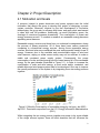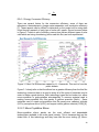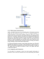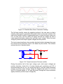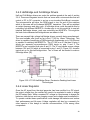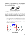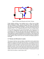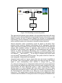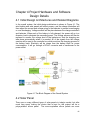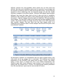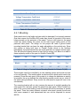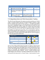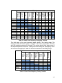
1
DEPARTMENT OF
ELECTRICAL & COMPUTER ENGINEERING
UNIVERSITY OF CENTRAL FLORIDA
EEL 4914
Senior Design I
Integrated Renewable Power System Controller
Group 28
Karel Castex
Julio Lara
David Wade
Jing Zou
Sponsored by Progress Energy
i
Table of Content
1.0 Executive Summary
2.0 Project Description
2.1 Motivation and Goals
2.2 Objectives
2.2.1 Small-Scaled
2.2.2 Self-Sustained
2.2.3 Efficiency
2.2.4 Environmentally Friendly
2.2.5 Low Maintence and User Friendly
2.2.6 Input 1: Solar Power
2.2.7 Input 2: Wind Power
2.2.8 Control Box
2.2.9 Energy Storage
2.2.10 Output
2.3 Project Requirements and Specifications
3.0 Research
3.1 Related Projects
3.2 Solar Power
3.2.1 Advantages and Limitations
3.2.2 Solar Cells and Manufacturing Technology
3.2.2.1 Mono-Crystalline Silicon
3.2.2.2 Polycrystalline Silicon
3.2.2.3 Thin Film and Amorphous Silicon
3.2.2.4 Copper Indium Gallium (de)Selenide (CIGS)
3.3.2.5 Cadmium Telluride CdTe Thin Film Panel
3.2.2.6 Gallium Arsenide GaAs Thin Film Panel
3.2.3 Photovoltaic Effect in Solar Cells
3.2.4 Photovoltaic Panel Performance
3.2.5 Solar Radiation
3.3 Wind Power
3.3.1 Advantages and Limitations
3.3.2 Wind Power Mechanism
3.3.3 Wind power Performance
3.3.4 Capacity and production
3.3.5 Distribution of Wind Speed
3.4 Charge Controllers
3.4.1 Shunt Controller
3.4.2 Series Controller
3.4.3 Maximum Power Point Tracking (MPPT)
1
2
2
3
3
3
3
3
4
4
4
5
5
5
5
8
8
8
8
9
10
11
11
12
12
13
13
14
15
17
17
18
19
19
22
22
24
24
26
ii
3.4.3.1 Perturb and Observe Method
3.4.3.2 Incremental Conductance Method
3.4.3.3 Constant Voltage Method
3.5 Rectifier
3.6 Voltage Regulator (DC/DC converter)
3.6.1 Buck Converter
3.6.2 Boost Converter
3.6.3 Inverting Buck-Boost Converter
3.6.4 Non-Inverting Buck-Boost Converter
3.6.5 Half-Bridge and Full-Bridge Drivers
3.6.6 Linear Regulator
3.6.6.1 78XX Three Terminal Linear Regulator
3.6.6.2 Zener Diode Regulator
3.7 Dump and Diversion Loads
3.8 DC/AC Inverter
3.8.1 Inverter Efficiency
3.9 Sensors
3.9.1 Voltage Sensor
3.9.2 Current Sensor
3.9.2.1 ACS712 Current Sensor
3.9.2.2 MAX4172 Current Sensor
3.9.2.3 CSLA2CD Current Sensor
3.9.3 Temperature Sensors
3.9.3.1 TMP3e6 Temperature Sensor
3.9.3.2 DS1624 Temperature Sensor
3.10 Microcontrollers Unit
3.10.1 Atmel ATmega328
3.10.2 Atmel AT91SAM7X512
3.10.3 Texas Instruments MSP430
3.10.4 PIC24 from Microchip
3.11 LCD Display
3.12 Analyzing Source Threshold Algorithm
3.13 Batteries
3.13.1 Types of Batteries
3.13.2 Lead Acid Battery
3.13.2.1 Limitations
3.13.2.2 Advantages
3.13.2.3 Types of Lead-Acid Batteries
3.13.3 Lithium Ion Battery
3.13.3.1 Limitations
27
28
29
30
33
34
35
36
37
39
39
40
41
42
43
44
45
45
46
46
48
49
50
50
51
52
53
53
54
54
55
56
58
59
60
60
60
60
61
61
iii
3.13.3.2 Advantages
3.13.4 Battery Charging Algorithm
4.0 Project Hardware and Software Design Details
4.1 Initial Design Architectures and Related Diagrams
4.2 Solar Panel
4.2.1 Mounting
4.3 Wind Power Generation
4.4 Controller Box
4.5 Monitoring System Design
4.5.1 Microcontrollers Units
4.5.2 Algorithm Implementation
4.5.3 LCD Display
4.5.4 Sensor Implementation
4.5.4.1 Voltage Sensor
4.5.4.2 Current Sensor
4.5.4.3 Temperature Sensor
4.6 Battery Bank
4.7 PCB Design
4.7.1 Design Equations for Printed Circuit Boards
4.8 DC/AC Inverters
4.9 Dump and Diversion Loads
5.0 Design Summary of Hardware and Software
5.1 Hardware Summary
5.2 Software Summary
6.0 Project Prototype Construction Plan
7.0 Project Prototype Testing
7.1 Solar Testing
7.2 Wind Testing
7.3 Microcontrollers and PCB testing
7.4 Sensor Testing
7.5 Integrating Solar and Wind Generation Testing
7.6 Storage Testing
7.7 Wind Generator Rectifier Testing
7.8 Voltage Regulator Testing
7.9 DC/AC inverting and Power Output Testing
7.10 Dump and Diversion Load Testing
8.0 Administrative Content
8.1 Milestone Discussion
8.2 Budget and Finance Discussion
8.2.1 Budget
61
62
65
65
65
67
68
71
75
75
77
80
81
81
83
84
85
88
90
92
93
96
96
96
101
103
103
104
106
107
109
110
111
112
112
113
114
114
118
118
iv
8.2.2 Finance Discussion
8.2.2.1 Final Client Price
8.2.2.2 Analysis of Profitability
Appendices
Appendix A - References
Appendix B - Copyright Permissions
Appendix C - Figures
Appendix D - Tables
119
121
123
i
iv
xvi
xviii
v
Chapter 1: Executive Summary
As the demand of renewable energy increases, solar and wind have become
more and more popular among all of the energy sources. However, due to the
unstable and uncontrollable nature of natural resources, relying on solar or wind
source solely may not be able to produce enough power to meet the demand.
Moreover, the performance of a solar or wind system independently can be quite
inconsistent. Therefore, in general, wind and solar are integrated together in a
power system synergistically to improve the overall stability. Nevertheless, in
reality, it is difficult to charge the battery using both wind and solar energy at the
same time. This is because source impedances of the wind generator and the
solar cell are very different. Moreover, wind and solar increase power system
variability and uncertainty. As a result, the group is motivated to design a
controller that will make the isolated integrated renewable power system more
efficient and stable.
The goal of this project is to design a controller that optimizes the performance of
an energy-efficient, standalone, renewable-energy-sourced integrated power
system. The group’s intention is to design a controller that is able to optimize the
performance of both energy sources, control the charging process, and monitor
the system in various conditions. The microcontroller-based controller will detect
the instantaneous variations of both wind and solar source, and then optimize the
charging operation through proper charge controllers. As a result, the entire
system of the integrated renewable power system (IRPS) contains a solar panel,
wind mill, control box, battery bank, and a power outlet to the loads.
In the overall system, the wind turbine and solar panels will collect powers and
feed them to the control box. Then control box will send the inverted power to the
battery bank for storage, or it will pass the power and feed it directly to the load
bus. The wind power charge controller has a rectifier that will convert AC power
which collected from the turbine into DC power and then store the power in the
Battery Bank. At the same time, Solar PV panels have a different and separate
solar charge controller. This controller will control the power coming from the
panels to the battery bank. The batteries will supply electricity when the wind
turbine and solar panel do not produce sufficient energy for the power
consumptions. Since most appliances and other house loads are usually run by
AC power, an inverter will be inserted to take DC power from the batteries and
convert it to 120 volt AC. Furthermore, for the excess power that cannot be
stored in the battery bank, a dump and diversion unit will divert it to a resistive
load.
Within the control box, several features will be added to make the operation on
the system more user-friendly and will facilitate the testing process in this project.
Three LCD screens, including a High Contrast LCD battery voltage, High
Contrast LCD turbine amperage meter, and Battery status LCD, will be attached
to the control box. The LCD screens will display the current live metrics of the
system to users as feedback.
1
Chapter 2: Project Description
2.1 Motivation and Goals
A common interest in power electronics and power systems was the initial
motivation that directs the group to develop this project of designing a power
system controller. Moreover, inspired by the fast development of innovative
technologies, the group aim to advance with times, and apply what was learned
in class with real life problems. Additionally, as world population grows, the
shortage of resources increases dramatically. The consumption of power and
energy increases as well. To conduct a research on renewable energy becomes
appealing more than ever.
Renewable energy sources are those have no undesired consequences during
the process of power production. All of them have lower carbon emissions
comparing to conventional energy sources. Among those renewable energy
sources, wind and solar are considered the most environmental friendly forms of
energy. However, due to the unstable and uncontrollable nature of wind and
solar resource, relying on either source solely may not be sufficient to make a
stable and consistent power supply system. Consequently, the power
consumption of solar and wind energy are the lowest among all of the renewable
energy for the past decade (illustrated in Figure 2.1). In order to increase the
consumption of solar and wind energy, a much more stable, consistent, and
reliable solar and wind power system need to be developed. One way to improve
the overall performance of the system is by integrating those two energy sources
together.
Figure 2.1 Monthly Consumption of renewable energy by fuel type, Jan 2000 –
Apr 2011. Permission requested from the U.S. Energy Information Administration
(2011).
While integrating the two energy source together may seem to be more reliable
of the single sourced system, there still exist elements that will influence the
2
overall stability and consistency of the power system. Therefore, in this project,
the goal is to design a controller that can optimize the overall performance of an
energy-efficient, standalone, renewable-energy-sourced integrated power system.
2.2 Objectives
The primary objectives of the overall system are small-scaled, self-sustained,
energy efficient, environmental friendly, low maintenance, and user friendly. All
elements within the system, such as microcontrollers, sensors, and monitoring
electronics devices should consume the lowest amount of power as possible.
2.2.1 Small-Scaled
The system will be small-scaled, and the purpose is to illustrate the idea of green
energy production for average home use.
2.2.2 Self-Sustained
One of the major objectives of the project is that the power system operates
independently from other power sources. The system will not be connected to the
power grid as well.
2.2.3 Efficiency
The most important purpose of the project is to design a controller that will
optimize the performance of the integrated system. In other words, it is to make
the system work more efficiently. With the intention of doing that, it is essential
for the controller to monitor the charging process of the battery and implement a
more efficient battery charging algorithm.
To make the charging process more efficient and easier to implement, the case
study conducted by Mu-Kuen Chen, Department of Electrical Engineering, at St.
John's University, Taiwan was adopted. In his conference paper “The Integrated
Operation of Renewable Power System,” he emphasizes the difficulty in
integrating wind and solar source with respect to the effect of source impedance.
He suggests setting different charging modes to optimize the charging operation
[1]. Therefore, the system will be able to charge the battery bank by using both
sources sufficiently.
2.2.4 Environmentally Friendly
The entire system should not produce any undesired consequences to the
environment. The use of renewable energy sources will reduce greenhouse gas
emission.
3
2.2.5 Low Maintenance and User Friendly
The system will be portable so that the user will be able to set up the system in a
remote location without any external power sources. The controller box will be
small in size. There will be three or more LCD screens on the controller box to
show the current live metrics of the system, including the input voltage, output
voltage, input voltage, output current, and battery charging status. Users can
monitor the system any time they want. Moreover, there will be buttons or
switches for the user to turn on or shut down the system manually as desired.
Minimum connections will be kept to the controller box so that there will be little
confusion at the set up process.
2.2.6 Input 1: Solar Power
Solar Power will be generated by a solar voltaic panel. This is rapidly becoming a
mainstream way to generate power in the commercial world as well as residential.
The main objective of this system is to charge and store energy efficiently into a
battery. Therefore the objective of the solar panel will be to help accomplish this
task. However the panel alone will not be the only component to complete this
task. The charge controller and voltage regulators attached to the output of the
solar panel will play just as big if not bigger role than the panel itself. With this
aside the goal for the solar panel will be to research as many different types of
panels and determine which one will be the most efficient choice for our region of
the country.
2.2.7 Input 2: Wind Power
Over the last few decades renewable energy has started to gain its ground. Of all
the different kinds of alternative energy sources available, the use of wind power
has been growing steadily. Wind generators are available for homeowners in the
market today, most of them relative easy to assemble. More homeowners chose
to have a wind generator to work along with PV panels to make their system
more productive. To make a wind generator working efficiently, homeowners also
need to purchase some extra equipment necessary such as, rectifiers to stabilize
the output AC current, charger controller to distribute the energy where most
needed, power divert, and DC-AC converter. However, among all these
components the most important in terms of efficiency is the charger controller.
Most of the charger controllers nowadays are composed of either simple
electrical components or are switch controlled systems. These systems usually
are wasting energy by distributing the excess current to the dump load or simply
do not charge the batteries efficiently. This design proposes a new way of
managing resources by implementing microcontrollers with smart algorithms that
charge the batteries faster and efficiently. For this reason a wind generator was
added to the design, to show that combined with PV panels the smart controller
will handle both sources smartly and efficiently
4
2.2.8 Control Box
Control box is the project definition for the consolidation of microcontroller unit(s)
and sensors which make possible to be knowledgeable about system status. The
sensors duty is being on top of system measurements at every moment and be
able to feed microcontroller inputs to allow data to be analyzed. Having the
microcontroller aware about what is happening in the system will create whole
system reliability since critical decision can be taken dodging painful situations
where some components can be seriously damaged and further causing system
malfunctioning. The control box is the brain with the responsibility of
accomplishing this project’s main purpose of maximizing energy harvested and
making the system work under optimal conditions.
2.2.9 Energy Storage
The performance of the batteries in a renewable energy system is the key to its
success. The main objective of the batteries is to maintain the consistency and
balance of energy within the renewable energy system. There will be two
batteries used in our Integrated Renewable Power (IRP) System to store the
energy that is collected by both the solar panel and the wind turbine when there
is an excess of supply. Both of the batteries will be used when the power collect
by solar panel and wind turbine is not sufficient enough to supply the loads, as
well. Therefore, the battery is required to have a large capacity so that users can
run the loads at any time as they desire. The battery-bank helps stabilize the
system by ensuring that there will be sufficient power supply to the load. The
batteries should be low cost, technological matured, and efficient.
2.2.10 Output
The output of the system should reach between 110 and 120 Volts in AC power
for the user to plug in electronic devices and run them. The outlet should be safe
for both the users and the electronic devices.
2.3 Project Requirements and Specifications
The operation of the system is required to be able to produce steady output
power and charging the batteries twenty-four hours a day in spite of the
variations of the solar and wind strength. All of the internal components should
consume as little power as possible. Moreover, the system must be safe both for
the user to operate on and the appliances to work with.
There are three categories of specifications, including power generation, control
box, and power charge, storage and delivery specifications. The input and output
of each component in every category are related with respect to the amount of
power flow in the system. The power generation specifications are shown in table
2.1 below.
5
Solar Panel
Output Power
>75W
Open Circuit Output Voltage
>12V
Short Circuit Output Current
>4A
Weight
< 20lb
Wind Turbine
Output Voltage
>12V
Output Power
> 450W
Generates power at
> 8mph
Size
Small
Table 2.1 Power Generation Specifications
The most important part of this project is the design of the control box. It major
parts of the control box are the microprocessor and the LED display. The
implementation of the design will be constructed on a custom ordered printed
circuit board (PCB). Table 2.2 shows the specifications of the microcontroller and
the LED in the control box.
Microcontroller
Clock Frequency
Low
Serial Ports
Yes
Programming Language
High level similar to C
Programming Memory
≥16K
Analog Pins
Yes
Digital input/output Pins
Yes
PWM Output Pins
Yes
Programming Debugging
Yes
Power consumption
Low, good sleep mode
LCD
Current Draw
Low
Voltage
Low
Lines Needed
1 to 3
Table 2.2 Control Box Specifications
In order to charge the battery, the power produced by both sources has to meet
the input requirement of the battery bank. Therefore, a DC/DC inverter will be
inserted at the input of the batteries. While with the purpose of powering
electronic devices with AC power, a DC/AC inverter needs to be inserted at the
out of the batteries.
6
Battery Bank
Voltage
12V
Depth of Discharge
75%
Lifespan Cycles
1000-2000
Efficiency
72-78%
Cost
Low
DC/DC Inverter (Voltage Regulator)
Maximum Voltage
> 15V
Output Voltage
> 12V
DC/AC Inverter
Continuous Max Power
1200 - 1500W
Input Voltage
12V
Output Voltage
110-120VAC
Table 2.3 Power Charge, Storage and Delivery Specifications
7
Chapter 3 Research
3.1 Related Projects
As the fast increasing demand of renewable energy, there are numerous
researches on making a more stable, consistent, and efficient. Among the
renewable energy related projects conducted by undergraduate university
students, almost 80 percent of the projects are on solar energy or wind energy
alone. Due to the intermittent and unpredictable nature of the renewable energy
source, depending either solar or wind energy source solely is considered
unstable and inefficient. Therefore, it was decided to improve the overall stability
and consistency by integrating the two energy source together.
A project conducted by a group of senior design students in University of Central
Florida has involved in integrating renewable energy. However, their design
involves human powered mechanism as one of the inputs [2]. This will increase
the system size and cost as a stand-alone renewable power system. Another
disadvantage in this project is that the group did not implement an efficient
battery charging algorithm. This disadvantage will lower the overall efficiency and
quality of the power system.
In addition, another group of senior design students provided more insight to the
maximum power point tracking for the solar system which satisfied the
requirements of the university’s senior design. The format of this paper will be a
reference of this documentation.
There is also a project that designed by University of Alaska Fairbanks. The
project is to develop a stand-alone generation system for an off-grid remote
community in Alaska by integrating renewable energy sources with existing fossil
fuel based generating system [3]. This project is designed for a larger scale.
Moreover, by integrating with the fossil fuel based generation, there will be more
emission produced by the system.
3.2 Solar Power
3.2.1 Advantages and Limitations
Solar power is an alternative power source that is both abundant and clean.
However solar power has a limitation which is the main reason it only accounts
for about 4% of the world’s electricity [1]. The biggest advantage to solar power is
that it emits no greenhouse gases, which makes it an incredibly attractive energy
source to help curb climate change effects on our planet. A good example of this
feat is Italy’s Montalto di Castro solar park which avoids 20000 tons of carbon
emissions a year [2]. Another enormous advantage for solar power is infinite free
energy. Solar does not require any raw materials such as coal or oil to be
continuously transported to the power plant adding more cost to the product.
8
The labor cost is also significantly lower at a solar power plant than a fossil fuel
one because the sun and the solar semi-conductors do most of the work. Solar
power is largely unaffected by the politics that endlessly drive the price of fossil
fuels up. The US gets a large amount of its oil from regions of the world that are
extremely volatile or unfriendly to US interests. Prices of fossil fuels have more
than doubled in the past decade due to price manipulation through wars and
politics [2]. However the sun is an unlimited source of energy and the price has
halved in the last decade, and will continue to decrease as the technology to
harvest it increases. Furthermore solar power doesn’t require us to mine raw
materials which destroy the environment. A terrible example of this is Canada’s
tar sands which is currently destroying the Boreal forest in Alberta which
accounts for 25% of the world’s intact forest. It also creates toxic pools of
byproducts that are large enough to see from space [3].
Despite all of the advantages that solar power has, there are just as many
disadvantages that hinder solar power’s use as a major power source. The most
obvious disadvantage is that solar energy cannot be harvested at night. This is a
big problem because during the winter months there are more hours of night than
that of day. Sometimes we are unable to collect the suns energy even during the
day due to weather and atmospheric disturbances. Another limitation is the
inefficiency of the solar panels ability to collect the sun’s the light. Currently solar
panel efficiency is around 22% which means a large quantity of surface area is
required to produce a significant amount of energy [2]. However technology is
tirelessly improving this number and will eventually no longer be a limitation to
solar power, but at this time it must be listed as a disadvantage. Another
limitation lies in the storage process which has not yet reached its potential. The
current solar drip feed batteries available are more suited for home use instead
of large scale solar power production [2]. The final and most important limitation
is the cost of installing solar panels. There is a large upfront cost and is the
equivalent to paying for 30 years’ worth of power just to install the system [2].
However technology will eventually help bring down this cost as it increases and
energy subsidies are put in place by governments around the world.
3.2.2 Solar Cells and Manufacturing Technology
There are many different types of materials used to make solar cells. All of them
vary in their cost and efficiency characteristics. For this project the design will be
looking for as high efficiency as can be possibly achieved while staying inside the
budget. The system will need to charge the batteries as quickly as possible
because there are only so many hours of day light each day. Solar panels are
broken up into two different categories, silicon and thin film. Silicon has been
around and studied much longer making it the more reliable of the two
technologies. The efficiency of the solar panels by definition is the ratio of
electrical output power to the amount of sunlight received. The equation for the
energy conversion efficiency can be seen below in EQ: 3-1 where 𝑃𝑚 (in W) is
the maximum power point, 𝐸 (in W/m2) is input light, and 𝐴𝑐 (in m2) is the surface
area of the panel [7].
9
∈=
EQ: 3-1 Energy Conversion Efficiency
𝑃𝑚
𝐸 ∗ 𝐴𝑐
There are several factors for the conversion efficiency; some of them are
reflectance, thermodynamic, charge carrier separation, and conduction efficiency
[7]. These aspects can be difficult to determine so the project will be using data
found through research of each type of solar cell’s specs. As can be seen below
in Figure 3.1 which is plot of efficiency versus time the two different types of solar
cells which are being considering (silicon and thin film) are both represented.
Figure 3.1 Best Cell Efficiencies created by L.L. Kazmerski. This work is from the
public domain.
Figure 3.1 clearly tells us that the silicon has a greater efficiency than the thin film
technology; however there is a need to study all of the types of materials used in
order to make a good decision. Both technology types can be broken into either
mono-crystalline or polycrystalline subcategories. A common material used in
making mono-crystalline thin film panels is gallium arsenide (GaAs) . Some
materials used to create polycrystalline thin film panels are; cadmium telluride
(CdTe), amorphous silicon (A-Si), and copper indium gallium selenide (CIGS) [8].
3.2.2.1 Mono-Crystalline Silicon
Mono-crystalline silicon panels are the most efficient and dependable
technologies available in the solar panel industry. This is because they are the
oldest form of this technology and they have had the most testing [4]. Mono10
crystalline solar cells tend to be around 17% efficiency and the other types
(polycrystalline and thin cell) are usually about 10% efficiency [9]. This high
efficiency means that mono-crystalline silicon will get the most watts per square
foot. Since the design will be limited on space and require high efficiency, monocrystalline silicon seems to be a good choice for this project. However despite the
high efficiency of this type of solar cell they can be very expensive. Monocrystalline panels are also difficult to install because they are extremely fragile
which can be an issue when the panels are being shipped to us as well [4].
3.2.2.2 Polycrystalline Silicon
Polycrystalline silicon as the name suggests is made of multiple silicon crystals
molded together to make one silicon panel. Polycrystalline or multiple crystal
panels are popular for residential use because of their low cost and average
efficiency [9]. As stated above the efficiency is not as high as mono-crystalline so
it has always been assumed that the mono-crystalline are superior, but this is not
necessarily true. After much time spent looking at different companies specs on
their products, it is clear that polycrystalline panels vary quite a bit from each
other and should be considered on a case by case basis. Some of the examples
that have been found include Conergy’s Powerplus P series modules have a
maximum efficiency of14.13% and Suntech’s polycrystalline Pluto technology
has been able to achieve a 20.3% [10]. These numbers were of course reached
in laboratory conditions, however they are still impressive. The prices for this type
of solar panels are perfect for our budget and will most likely be the panel type
used for this project.
3.2.2.3 Thin Film and Amorphous Silicon
Thin film and amorphous silicon panels are the newest generation of solar
technology. Thin film panels can be produced out of many different compounds
that were mentioned earlier in this chapter. Once the thin film is manufactured it
is usually placed between two glass panels to protect it, this will make the thin
film panel quite a bit heavy then its silicon counterparts. The semiconductor is
place between the glass plates. A flexible laminate can also be used to protect
the semiconductor. The laminate is becoming more commonly used in thin film
panels making them cheaper and faster to produce, because the entire panel is
considered a solar cell.
There are many advantages to using thin film technology. The laminate makes
them flexible and easier to mount on uneven surfaces. This means that thin film
panels are also more durable from weather damage. If a thin film panel is
damaged it will still work at a lesser rate. This is not true with silicon solar panels,
when one cell is damaged the entire panel will not work at all. The use of
laminate thin cells can also be more useful in residential applications because
the traditional roofing materials can be replaced all together with the thin film
panels. This is possible because of how much less thin cells weigh compared to
its silicon counterpart. Thin film panels also work much better under hot
conditions. They will not lose nearly as much efficiency as the temperature
11
increases. This makes thin film cells a good choice for hotter climates such as
the Southwestern region of the United States. Thin film panels also perform
better than the competition in the shade and low light conditions. However thin
film and amorphous silicon also have some disadvantages.
The most significant of those disadvantages is their efficiency. Thin film panels
range around 4% - 7% efficiency [11]. This means that more than twice as many
thin film panels are required to produce the same amount of power as its silicon
competitors. This is the main reason thin film technology has not replaced the
silicon technology. The efficiency has not quite matured yet, but it could surpass
the efficiency of the silicon panels by 2020 [11]. As exciting as this new
technology is it will be difficult to implement it in this project at its current
efficiency level. The silicon panels will be needed for more testing due to the
inherent inefficiencies of thin film technology.
3.2.2.4 Copper Indium Gallium (de)Selenide (CIGS) Thin Film
Copper Indium Gallium Selenide or CIGS is another type of thin film
semiconductor material. CIGS is a material that strongly absorbs sunlight thus
requiring a much thinner film than other semiconductor materials. CIGS
absorption coefficient (105/cm for 1.5 eV) is higher than any other semiconductor
used for solar panels. CIGS is mainly used in the form of polycrystalline thin films
and the best efficiency was achieved in December of 2005 at 19.5% [17]. Higher
efficiencies around 30% can be achieved with the use optics to concentrate the
sunlight onto the panels. The market grew for this PV at a 60% annual rate from
2002 to 2007 [16]. Like other thin film panels the CIGS compound is layered on a
glass back plate. Since so little of the material is needed the CIGS thin film
panels are extremely light weight. Due to the ever increasing efficiency
associated with CIGS panels their production is projected to increase rapidly in
the future. Unfortunately these panels tend to be extremely expensive due to
their vacuum based fabrication process [17]. Therefore CIGS thin film panels will
not be considered for the solar panel of the project.
3.3.2.5 Cadmium Telluride CdTe Thin Film Panel
Cadmium Telluride or CdTe was one of the orginal materials used in thin film
technology to try and improve the low efficiencies experienced with amorphous
silicon. Like CIGS, CdTe is also manufactured on a glass substrate. CdTe is the
most common and the most cost effective type of thin film technology on the
market currently. Similar to CIGS CdTe panels perform better in the shade and
low light conditions than silicon does. Unfortunately CdTe panel’s efficiency
maxed out in 2001 at 16.5%, and their average efficiency is around 7% to 12%
[18]. Another disadvantage to the CdTe thin film technology is that Cadmium is
extremely toxic and Tellurium supplies are scarce. This leads to CdTe panels
being exceedingly expensive and toxic to people and the environment.
12
3.2.2.6 Gallium Arsenide GaAs Thin Film Panel
The final type of solar panel to be discussed in this research is Gallium Arsenide
or GaAs thin film panels. Like CdTe panels, GaAs panels are extremely
expensive and toxic. Gallium is an extremely rare material and Arsenic is a very
poisonous substance. People can become very sick and possibly die if the panel
gets damaged and the semiconductor is exposed. However the efficiency of a
GaAs thin film solar panel is quite a bit higher than that of a CdTe panel. GaAs
efficiency averages around 20% to 25%, with a record near the 30% mark [19].
This is because GaAs as a semiconductor material has a nearly ideal band gap.
Like the other thin film types of material, GaAs has insensitivity to heat thus
helping the efficiency rating. Not only is GaAs resistant to heat, but it is also
resistant to radiation. This makes GaAs solar panels ideal for space applications.
However the disadvantages of GaAs far outweigh the benefits and will not be
further pursued for this project.
3.2.3 Photovoltaic Effect in Solar Cells
To help make the decision of which type of solar panel would fit the needs of this
project this paper will have to discuss how the solar cell actually works briefly.
Solar cells are made of semi-conductors which respond to the sun’s light. The
determining factor of how the semi-conductor will respond is the band gap [13].
Silicon or Germanium is the most common types used because they are
abundant and engineers understand how they respond quite well. The sun’s light
is made up of different types of light which have different energies levels. There
is the low energy infra-red light, the intermediate energy visible light, and the high
energy ultra-violet light. The Earth’s atmosphere and magnetic field protect us
from the harmful ultra-violet light so solar panels on the surface of the planet
don’t need to worry about this type as much. No one semi-conductor has a band
gap that can respond to the full range of the sun’s light [13]. Solar panels have
been invented that can respond to the full spectrum of the sun’s light by layering
different types of semi-conductors with different band gaps in series [13].
However the manufacturing process of these panels is extremely difficult and
expensive, therefore they are not readily available to the consumer market.
The solar panels which are in the consumer market are usually made up of one
or two types of semi-conductors which can have their band gaps modified by
different doping techniques [12]. When the photons hit the solar cells the semiconductors will absorb the photons that have energy equal to or greater than that
of the band gap. This promotes electrons in the conduction band which is how
energy is produced in the cell. If the photon’s energy far exceeds the band gap
the energy will be dissipated off as heat and if the energy is much smaller the
photon will just pass through the solar panel and no energy will be collected from
it [12]. Obviously the goal of the solar panel is to produce power so the solar
panel needs to create current and voltage from the photons to make power.
13
There are two important parameters for both the current and the voltage. The
current has Isc (short-circuit current) and Imp (maximum-power current), the
voltage has Voc (open-circuit voltage) and Vmp (maximum-power voltage). Vmp
and Imp are the parameters that best express the performance of the solar cells
which is called the fill factor. The fill factor should be around 80%-90% for high
efficiency solar cells. The ultimate goal is to choose a semi-conductor material
that has an optimal band gap near the middle of the energy spectrum. This will
ensure that the panel can collect the highest possible amount of solar radiation
that the selected material is capable of obtaining.
3.2.4 Photovoltaic Panel Performance
Solar cells can be extremely inefficient which was talked about in the previous
sections. Further research will be needed to examine the other factors that will
affect the panel outside of the physics of the semi-conductors and ascertain any
possible ways to increase the performance of the panels. Some of the issues
being examined are the electron-hole recombination rate, temperature effect, and
the light absorption efficiency. The impurity concentration of the polycrystalline
silicon will increase the electron-hole rate which will result in a decrease of the
panel efficiency. This is the main reason mono-crystalline panels perform better
than polycrystalline [14].
Temperature is another factor that can negatively affect the performance of the
solar panel. Contrary to popular belief, the efficiency of the solar panel decreases
as the temperature increases [14]. This occurs because the magnitude of the
electric field at the p-n junction is reduced due to the temperature increasing the
conductivity of the semi-conductor. This will result in a disruption of the charge
separation causing a lower voltage across the cell [14]. However the higher
temperature will cause the electron mobility to increase which will cause a slight
increase in current, but this is insignificant in comparison to the voltage loss. The
optimal environment for a solar panel to operate is sunny and cold temperatures.
Unfortunately for this system it is being built in an area that does not get cold
often. Some improvements could be added such as adding a coolant system to
the back of the panel, but this is costly and time consuming. The temperature
effect will have to be kept in mind for any inefficiencies that are noticed. Most
solar panel manufactures will include a temperature coefficient in the specs of
their product to allow the customer to have an idea of the panel’s efficiency in
certain temperatures. Figure 3.2 depicts the temperature effect on PV panels
below.
14
Figure 3.2 Temperature effect on PV panel performance with permission of
solarpower2day.net
The last inefficiency is light absorption which was discussed in the earlier section.
The semi-conductors can only absorb photons that have energy equal to or
greater than their band gap. This results in quite a bit of lost energy due to light
having a different energy. Many solar panel companies will engage in band gap
engineering which will maximize the amount of light the solar panel is able to
absorb. The design engineer can choose to create smaller band gaps to capture
the lower energy photon. However the lower energy light will result in a lower
voltage. The engineer could increase the band gap to gather more of the higher
energy photons, but the panel will not absorb the lower energy level photons
causing a lower current. A balance has of these two different ways of band gap
engineering must be found to ensure an optimal solar panel. Another thing to
remember is that much of the light is lost due to reflection. This is why most solar
panels will have a layer of anti-reflection material on top of them to minimize this
negative effect.
3.2.5 Solar Radiation
Solar radiation is the electromagnetic radiation that is emitted from the sun and is
collected by the solar panel to produce power. Solar radiation is measure in
kilowatt-hours per square meter per day (kWh/ m2/day). Figure 3.3 below shows
the annual solar radiation of the United States. As can be seen in the figure the
best location for solar power in the country is the southwestern region with
around 7.5-8.0 kWh/ m2/day. Central Florida averages per year around 5.5-6.0
kWh/ m2/day according to the figure below [15].
15
Figure 3.3 Annual Solar Radiation of the United States with permission from
NREL.
There are many different methods to optimize the solar radiation collected by the
solar panel. Some of those methods include preprogramed angles for each hour
of daylight, solar tracking/ light concentration, and MPPT (Maximum Power Point
Tracking). The first method is exactly how it sounds. The solar panel is mounted
on a double axis mechanism and is moved to pre-determined angles for each
hour of day light. Solar tracking also requires the solar panel to be mounted on a
double axis mechanism with its movement controlled by the sun’s intensity. The
light concentration implements mirrors or lenses around the panel to intensify the
light’s concentration. The MPPT system is a more indirect approach that controls
the photovoltaic output voltage and current to optimize the efficiency. An
example would be if the battery requires a larger voltage the MPPT system will
recognize this and increase the output voltage while decreasing the output
current to maintain the same photovoltaic power level.
16
3.3 Wind Power
3.3.1 Advantages and Limitations
Wind power is a natural resource that is free, unlimited and renewable. Welldesigned blades can capture wind more efficiently to maximize rotor’s output
current. All this energy produced by the turbines it’s free of any type of emissions
or other pollutants that may create greenhouse gases.
Since wind turbines come in a wide range of sizes, they can be used by anyone
to produce their own additional input power for their household use. Usually,
private companies create wind farms to produce up to 1000MW of electricity.
However, remote areas that are not connected to the electricity power grid can
create their own wind farm to supply their own demand of electric power.
Due that the space required to install a wind turbine is very minimum, wind farms
can have hundreds of wind turbines. Wind farms do not use very much surface
space; in the case of agriculture, this allows to farmers performing ground
activities without complications.
Many land owners benefit from wind turbines when a company plans to create
wind farm. Companies have to pay for the space that their wind turbines use.
This is a great, complementary, source of income that boosts local economies. In
addition, many people view wind farms as an interesting feature that enhance the
landscape.
As there are great benefits from the generation of electric power through wind
turbines, there are some limitations and disadvantages. Wind has an immense
power but is not continuous and constant. Winds may vary from zero to hurricane
force winds. This factor unleashes other subsequences. The production of
electricity is not constant and cannot be predictable all the times. Moreover, if a
wind turbine gets exposed for long periods to strong winds, this can break apart
the whole wind turbine and reduce production of electric power.
One major challenge to the industry of wind power generation is that to create
enough electricity for a small community of 50,000 people they need to install
hundreds of wind turbines. How many wind turbines would be required to satisfy
the demand of larger community for instance 120,000 people? Space is a key
factor that will always be taken into consideration when building new wind farms.
Some people argue that wind turbines, when active, produce high level of noise.
This can get challenging to solve when all wind turbines are combine to create
wind farms. However, technology has improved wind turbines and now they are
much more quiet machines.
Some other people think that wind farms are grotesque in form and shape. They
feel that the landscape is being changed completely by the creation of wind
farms. Natural view of countryside and coastal landscape are not enjoyable
17
because they are being corrupted by large and tall structures that never
belonged to the country side.
3.3.2 Wind Power Mechanism
Generating electricity from wind is relatively simple. All effective wind turbines
often have 3 blades that are aerodynamically constructed to easily create a
rotating movement as air blows. The blades spin a shaft that is linked to a
generator that creates the electricity.
When the wind blows, the blades create a lift, similar to the wings of airplanes
and the blades begin to rotate. When the blades rotate, a low-speed shaft is
spanned 30 to 60 times in a minute. This low-speed shaft is connected with a
gearbox or a high-speed shaft that accelerates the rotation to 1000 to 1800
rotation in a minute. The high-speed shaft drives the generator and produces
electricity. The generator is then connected to an electric power grid.
Generating the Power:
Four factors determining the electricity capacity of a wind turbine is wind velocity,
tower height, air density and blade radius.
Wind velocity determines energy generated. Wind is never even, sometimes
strong and other times weak. However, wind turbines do not operate in too
strong or weak winds. If the speed is too low, for example, below 8 miles per
hour the turbines will not work. The ideal speed is winds in the range of 25 to 55
mph. If the wind goes above 55mph the turbine is switched off as damage can be
caused.
A tall turbine is usually more efficient. There are two reasons for this, being that
more winds can be captured at higher altitudes and there is less turbulence
(winds are more constant).
Air density determines the kinetic energy of winds. The more dense the winds the
more capacity do they have to propel the turbine to turn. In high-altitudes the air
pressure is lower, in other words the air is lighter and is thus less effective
location for wind turbine to operate. In lower-altitudes such as near the sea level,
the air is dense and heavy making it much more effective to turn the wind turbine.
The radius of the blades determines the amount of wind that can be harvested. A
large blade will be able to yield much more wind and thus the diameter of the
blade can as substantially establish power levels. [20]
18
Figure 3.4 Wind Generator Mechanisms
3.3.3 Wind power Performance
Ideally, our project would work for a combined system of wind power and solar
energy that both combine will deliver up 1.5 kW for a typical household. To
satisfy this demand, a wind turbine capable to deliver up 1KW at 24 V will be
needed. There are many products in the market that with such specification that
would fit for our project. However, the prices of an standard wind turbine that
delivers up to 1KW range from $800 to $1000. Our budget is very limited and
acquiring such turbine will leave us in negative. Since, our main goal for this
project is to build an integrated circuit box that controls input power from solar
and wind energy, stores the energy, manage the excess of energy, and delivers
energy efficiently; the wind turbine will be scaled down.
For testing and illustration purposes, a wind turbine that delivers from 250 to 400
Watts will work perfectly for our project. These turbines vary in price from $130 to
$400. This input power combined with solar energy will be enough to change the
12V battery bank and deliver the excess to load if the system has some
components plugged in.
3.3.4 Capacity and Production
For this project it is important to know how much capacity wind power is
produced in the US since the controller box can be utilized along with installed
19
wind turbines. Capacity and production are two of the main factors that make
wind power more attractive as an alternative source of electricity, today.
According to the Global Wind Energy Council or GWEC, the new global total
capacity at the end of 2011 was 238 GW, representing cumulative market growth
of more than 20%, an excellent industry growth rate given the economic climate,
even though it is lower than the average over the last 10 years, which is about 28%
[21]. In the United States, the posted annual market growth of more than 30% in
2011, adding 6,810 MW in 31 states for a total installed capacity of almost 47
GW, and cumulative market growth of nearly 17%. While the US market
struggles with uncertainty surrounding the extension of the federal Production
Tax Credit (PTC), wind power is now established in 38 states, and the footprint of
the US turbine and component manufacturing industry covers 43 states. This
means that US manufacturers were able to supply about 60% of the content for
the US market in 2011, up from just 25% a few years ago. All things point
towards more growth in 2012, although this is clouded by dim prospects for the
2013 market, depending on the fate of the PTC [22].
So far this year, according to the AWEA, 2,800 megawatts (MW) of wind, along
with 1,400 wind turbines have been installed across the US, helping the wind
industry reach this fantastic achievement. Many of the new installations have
come from new projects in Nevada, Idaho, Iowa, Hawaii Oklahoma, and
California. Some of the key projects that are going in across six of these states,
according to the AWEA include: Pattern Energy’s Spring Valley wind farm, 30
miles east of Ely, Nevada (151.8 MW). Enel Green Power North America’s Rocky
Ridge wind farm in Oklahoma (148.8 MW). enXco’s Pacific Wind project in Kern
County, California (140 MW). Utah Associated Municipal Power’s Horse Butte
project in Idaho (57.6 MW). First Wind’s Kaheawa Wind II wind farm in Hawaii
(21 MW) [23].
What has occurred in the wind industry with the US reaching that plateau is quite
remarkable. Consider that between 1981 and 2003, 5 GW of wind power was
generated. That number doubled to 10 GW by 2006, then 25 GW by 2008, and
now 50 GW in 2012. Also, Nuclear energy was the last new energy technology to
reach 50 GW, done in the late 1970’s and 1980’s.
Wind potential is enough to take out coal power plants in the US. 50 GW of wind
provides the same amount of energy as 44 coal fire power plants, or 11 nuclear
power plants. The future potential to move at a lightning-fast pace and replace
these sunset energy sources is very realistic, especially when you consider that
39 states now have utility-sized wind farms, according to the AWEA.
20
Figure 3.5 AWEA Infographic
In August of 2012, the Energy Department released a new report highlighting
strong growth in the U.S. wind energy market in 2011, increasing the U.S. share
of clean energy and supporting tens of thousands of jobs, and underscoring the
importance of continued policy support and clean energy tax credits to ensure
that the manufacturing and jobs associated with this booming global industry
remain in America According to the 2011 Wind Technologies Market Report, the
United States remained one of the world’s largest and fastest growing wind
markets in 2011, with wind power representing a remarkable 32 percent of all
new electric capacity additions in the United States last year and accounting for
$14 billion in new investment. According the report, the percentage of wind
equipment made in America also increased dramatically. Nearly seventy percent
of the equipment installed at U.S. wind farms last year – including wind turbines
and components like towers, blades, gears, and generators - is now
from domestic manufacturers, doubling from 35 percent in 2005. The growth in
the industry has also led directly to more American jobs throughout a number of
sectors and at factories across the country. According to industry estimates, the
wind sector employs 75,000 American workers, including workers at
manufacturing facilities up and down the supply chain, as well as engineers and
construction workers who build and operate the wind farms.
21
Technical innovation allowing for larger wind turbines with longer, lighter blades
has steadily improved wind turbine performance and increased the efficiency of
power generation from wind energy. At the same time, wind project capital and
maintenance costs continue to decline, driving U.S. manufacturing
competitiveness on the global market. For new wind projects deployed last year,
the price of wind under long-term power purchase contracts with utilities
averaged 40 percent lower than in 2010 and about 50 percent lower than in 2009,
making wind competitive with a range of wholesale power prices seen in 2011.
Despite these recent technical and infrastructure improvements and continued
growth in 2012, the report finds that 2013 may see a dramatic slowing of
domestic wind energy deployment due in part to the possible expiration of federal
renewable energy tax incentives. The Production Tax Credit (PTC), which
provides an important tax credit to wind producers in the United States and has
helped drive the industry’s growth, is set to expire at the end of this year. The
wind industry projects that 37,000 jobs could be lost if the PTC expires. Working
in tandem with the PTC, the Advanced Energy Manufacturing Tax Credit
provides a 30 percent investment credit to manufacturers who invest in capital
equipment to make components for clean energy projects in the United States.
President Obama has called for an extension of these successful tax credits to
ensure America leads the world in manufacturing the clean energy technologies
of the future. [24]
3.3.5 Distribution of Wind Speed
The strength of wind varies, and an average value for a given location does not
alone indicate the amount of energy a wind turbine could produce there. To
assess the frequency of wind speeds at a particular location, a probability
distribution function is often fit to the observed data. Different locations will have
different wind speed distributions. The Weibull model closely mirrors the actual
distribution of hourly wind speeds at many locations. The Weibull factor is often
close to 2 and therefore a Rayleigh distribution can be used as a less accurate,
but simpler model.
Power generation from winds usually comes from winds very close to the surface
of the earth. Winds at higher altitudes are stronger and more consistent. Recent
years have seen significant advances in technologies meant to generate
electricity from high altitude winds. [25]
3.4 Charge Controllers
The main reason a system needs a charge controller is to protect the battery
from overcharge and over discharge. Systems that have small, predictable, and
continuous loads may be able to operate without a charge controller [26].
However solar and wind power are nowhere near being predictable or continuous
so the design will need to implement charge controllers to help our batteries
charge efficiently and without damaging them. As was discussed in earlier parts
22
of this chapter, solar disadvantages are when the sun is not out, the weather is
interfering, and the wind is not continuously blowing. Implementing an efficient
charge controller will allow us to overcome the inherent shortcomings of wind and
solar power. A correctly operating charge controller will also prevent overcharge
or over discharge of the battery regardless of temperature or seasonal change in
the load profile, which will be another major reason for applying this component
into our system.
There are many different algorithms used for the different types of charge
controllers, but they all have the same basic parameters. The manufacturer will
usually give you these parameters in their spec data sheets which give the limits
such as load currents, losses, set points, and set point hysteresis values. The set
points are usually dependent on the temperature of the controller and the
magnitude of the battery current [22]. There are four basic charge controller set
points which are; Voltage Regulation set point (VR), Voltage Regulation
Hysteresis (VRH), Low Voltage Disconnect (LVD), and Low Voltage Disconnect
Hysteresis (LVDH).
The voltage regulation set point is the maximum voltage that the controller will
allow the battery to reach. The controller will either discontinue battery charging
or begin to regulate the amount of current being sent to the battery once this
point has been hit [27]. The voltage regulation hysteresis is the difference
between the VR set point and the voltage at which the full array current is
reapplied. The greater this voltage span, the longer the array current is
interrupted from charging the battery. If the VRH is too small, then the control unit
will oscillate, possibly harming the switching element or any loads attached to the
system [26]. This is an extremely important factor to the entire system and will
have to be monitored closely or the charging effectiveness of the controller will
suffer.
The low voltage disconnect is the voltage point at which load is disconnected
from the battery to prevent over discharge. In other words the LVD is the actual
allowable maximum depth of discharge and available capacity of the battery.
The LVD does not have to be temperature compensated unless the battery is
operating below 0°C [26]. Similar to the VRH the LVDH is the difference between
the LVD set point and voltage at which the load is reconnected to the battery. If
the LVDH is too small, the load will rapidly cycle on and off at low battery stateof-charge which can damage the controller. If the LVDH is too large, the load
may remain off until the array fully recharges the battery [26]. A large LVDH
could increase battery health due reduced battery cycling. However the
availability of the load would be sacrificed. All four of the set points described
above will have to be analyzed in depth as the charge controller is put through
the design phase of the project. The set points are crucial to the health of the
battery and charge controller.
23
3.4.1 Shunt Controller
After discussing the basic theory of the charge controller above the methods of
actually controlling the charging of the battery should be examined. There are
two basic methods that could be utilized for this project and they are series and
shunt regulation. Both of these methods can be highly effective for the charge
controller with each having benefits and limitations. First the shunt controller
method, which is tends to be designed for PV systems with currents less than
20A. The shunt controller interrupts the current by short-circuiting the array to
regulate the charging of the battery. This could cause the battery to short-circuit
as well so a blocking diode will be needed in series between the battery and the
switching element. This controller type also requires a large heat sink to dissipate
the excess power [26]. The shunt controller can be split into two different
algorithm types; linear and interrupting. The shunt linear algorithm maintains the
battery at a fixed voltage by using a control element in parallel with the battery.
This relatively simple design is usually implemented with a Zener power diode
which can drive the cost up and limit the power ratings of the controller [22]. The
shunt interrupting algorithm is a more typical use of a shunt controller by simply
short-circuiting the PV array to terminate battery charging. Shunt interrupting
method is also known as pulse charging [27]. The figure below depicts the daily
profile of the shunt interrupting controller.
Figure 3.6: The Daily Charge Profile of a Shunt-Interrupting Controller.
Permission from American Technical Publishers Pending
3.4.2 Series Controller
The series controller uses some type of control element in series between the
solar array and the battery. The series controllers, like shunt controllers can be
broken down into two different subcategories; interrupting and linear. The
interrupting series controller typically will use a blocking diode for the switching
element and the controller will open the circuit to terminate the battery from
24
charging. There are many different algorithms for the interrupting series controller
such as 2-step constant current, 2-step dual set point, pulse width modulation,
and sun-array switching. All these different algorithms essentially accomplish the
same task inside the charge controller. The daily charge profile of the
interrupting series controller can be seen in the figure below.
Figure 3.7: The Daily Charge Profile of a Series-Interrupting Controller.
Permission from American Technical Publishers Pending
The second type of the series controller is the linear series. The linear series
controller has two subcategories which are; constant voltage and constant
current modified. The constant voltage algorithm will dissipate the balance of the
power that is not used to charge the battery. This type of algorithm is highly
effective for a system that is using a valve regulated (sealed) battery [26]. This is
the type of battery that will most likely be used for this project therefore this type
of algorithm will be the first one to be tested for the charge controller. The last
series algorithm is the constant current one. This is a multi-step algorithm that
switches to a preset constant current rate to control the charging of the battery.
The battery voltage is then set to a specific voltage which depends on the
chemistry of the battery. The charge rate will then return to constant current
linearly as the battery voltage decreases [27]. The daily charge profile of the
series linear controller can be seen below.
25
Figure 3.8: The Daily Charge Profile of a Series-Linear Controller. Permission
from American Technical Publishers Pending
3.4.3 Maximum Power Point Tracking (MPPT)
Maximum power point tracking or MPPT is a technique used in a charge
controller for getting the maximum voltage possible out of the solar array. Solar
cells have a non-linear output voltage which is known as the I-V curve. This is
due the complex relationship between the solar cell, solar irradiation,
temperature, and total resistance. It is the purpose of the MPPT system to
sample the output of the cells and apply the proper resistance (load) to obtain
maximum power for any given environmental conditions [37]. The fill factor is a
parameter that deals with this non-linear electrical behavior. The fill factor (FF) is
defined as the ratio between maximum power of the solar cell to the product of
the open circuit voltage (Voc) and the short circuit current (Isc). Therefore the
maximum power can be calculated with this equation 3.2 shown below [37].
𝑃 = 𝐹𝐹 ∗ 𝑉𝑜𝑐 ∗ 𝐼𝑠𝑐
Equation 3.2- Formula for Maximum Power
Now that the maximum power has been explained it is easier to understand
where the maximum power point is located. Since P=V*I the maximum power
point location can be determined through simple calculus. Therefore the
maximum power point location can be defined as dP/dV=0 [37]. This means that
the maximum power point location is at the knee of the I-V curve. The purpose of
the MPPT system is to track this location for the maximum power. The MPPT can
be seen below in Figure 3.9 intersecting all the I-V curves at the maximum power
location during varying sunlight.
26
Figure 3.9: Solar Cell I-V Curve in Varying Sunlight. Permission from Creative
Commons
There are several common methods that are used to implement maximum power
point tracking. These approaches all vary on complexity based on the type of
tracking they utilize. The three most common types that will be talked about in
this research paper are: Perturb and Observe Method, Incremental Conductance
Method, and Fixed Voltage Method [37].
3.4.3.1 Perturb and Observe Method
This method of power point tracking constantly checks the voltage or current
(depending on the system) and continuing to increase the voltage as long as the
power continues to increase [38]. After the maximum power point has been
passed the algorithm will notice the power dropping and start to decrease the
voltage to compensate. Figure 3.10 depicts the algorithm iterating over the power
curve.
27
Figure 3.10: MPPT Perturb and Observe Method Permission from American
Technical Publishers
The main disadvantage of the Perturb and Observe algorithm is that it has
difficulties when dealing with low irradiance. This is due to the algorithm
oscillating around the maximum power point which inevitably leads to
inefficiencies. Another disadvantage is when the power curve flattens out the
Perturb and Observe Method has trouble determining where the maximum power
point actually is located. The final disadvantage to be discussed is that the
algorithm has difficulty dealing with rapidly changing conditions. This can
sometimes lead to the algorithm to take iterations in the wrong direction [39].
Despite all the disadvantages, this algorithm is the most commonly used MPPT
method because of its simplistic design.
3.4.3.2 Incremental Conductance Method
Another MPPT algorithm that is a bit more accurate and complex is the
Incremental Conductance Method. The main idea of this algorithm is to compare
the differentiation of the power with respect of voltage to zero and determine if it
is greater than or less than zero. This algorithm can be seen in Figure 3.11,
notice how the differential is less than zero after the maximum power point
location and is greater than zero before it.
28
Figure 3.11: MPPT Incremental Conductance Method Permission from American
Technical Publishers
The algorithm will know when the maximum power point location has been found
when dP/dV=0 [39]. Unlike the perturb and observe method, a discreet value is
determined for the maximum power point location in Incremental Conductance
method. This system will remain at this point until it undergoes a change in the
environmental conditions affecting the power [39]. The big advantage in this
method over the perturb and observe method is that the inequality determine
from calculating the derivative gives a direction. This will prevent the algorithm
from incrementing in the wrong direction.
3.4.3.3 Constant Voltage Method
Constant Voltage Method is the simplest of the three common MPPT algorithms.
This algorithm operates as a constant voltage value based of the open circuit
voltage. There is a range of accepted approximations for the operating voltage
which in between 73% and 80% [39]. Figure 3.12 below illustrated the algorithm
at a constant voltage of 76% of the Voc.
29
Figure 3.12: MPPT Constant Voltage Method Permission from American
Technical Publishers
The constant voltage algorithm will temporarily set the solar panel current to zero
to determine the open circuit voltage. The operating voltage is then is then based
of the ratio of the constant voltage to that of the open circuit voltage. This is
where the system will begin moving. A specified time must be entered into the
algorithm to tell the system when to isolate the source and begin the operation
again [39]. This method is not as efficient as the perturb and observe or the
incremental conductance methods. When the current is set to zero by the
system significant losses of efficiency occur because so much energy is wasted.
The only advantage to this algorithm is that is much more simple and spends
less time on the computations within the system [39].
3.5 Rectifier
Wind generators do not produce DC electricity, so a device called a rectifier is
used to convert the turbine's output current to DC. This is the first stage in the
battery charger circuit. Some turbines have a rectifier built in. In most cases
though, the rectifier is supplied as a separate component that must be installed
between the wind turbine and the battery charger. Often, the rectifier is combined
with a charge controller into one complete wind turbine control unit
Rectification is the process of converting an alternating (AC) voltage into one that
is limited to one polarity. The diode is useful for this function because of its
nonlinear characteristics, that is, current exists for one voltage polarity, but is
essentially zero for the opposite polarity. Rectification is classified as half-wave
or full-wave; with half-wave being the simpler and full-wave is being more
efficient.
30
Figure 3.13 Rectified Sine Wave. Permission Pending.
The full-wave rectifier inverts the negative portions of the sine wave so that a
unipolar output signal is generated during both halves of the input sinusoid. The
input of the rectifier consist of a power transformer, in which the input varies from
0 to 15 volts (rms), and 0 to 60Hz AC signal, and the two outputs are from a
center-tapped secondary winding that provides equal voltage. When the input
voltage is positive both output signals voltages are also positive.
The input power transformer also provides electrical isolation between the power
line circuit and the electronic circuit to be biased by the rectifier. This isolation
reduces the risk of electrical shock.
Np
C0
D2
Figure 3.14: Texas Instruments Full-wave rectifier
During the positive half of the input voltage cycle, both output voltages are
positive; therefore, diode D1 is forward biased and conducting and D2 is
reversed biased and cut off. The current through D1 and the output resistance
produce a positive output voltage. During the negative half cycle, D1 is cut off
and D2 is forward biased, or “on” and the current through the output resistance
again produces a positive output voltage [28].
31
Another alternative for rectifying input ac signal is the full-wave bridge rectifier.
This circuit, which still provides electrical isolation between the input aa powerline
and the rectifier output, but does not require a center-tapped secondary winding.
However, it does use four diodes, compared to only two for the regular full-wave
rectifier circuit. During the positive half of the input voltage cycle, the voltage
across the rectifier input is positive, and D1 and D2 are forward biased, D3 and
D4 are reversed biased, and the direction of the current is towards D1 and D2.
During the negative half-cycle of the input voltage, the voltage across the rectifier
input is negative, and D3 and D4 are forward biased. The direction of the current
towards D3 and D4 produces the same output voltage polarity as before. Since
the full-wave bridge rectifier is more efficient when delivering converted ac power,
this will be used for the project.
Q3
Q2
D1
+
+
L1
C0
Np
D2
Q4
Q1
Figure 3.15 Texas Instruments Full Bridge Controller
As the voltage runs through the diodes it becomes a form of DC voltage, along
with pulsations of up and downs, which is called as ripple voltage. For this project
the charging circuit requires a steady state DC input free from ripple voltage. A
RC circuit can be added that soothes out these ripples and improve quality of
rectified output.
32
Figure 3.16 RMS Ripple Voltage
3.6 Voltage Regulator (DC/DC Converter)
Voltage regulators or DC to DC converters are necessary because the DC
voltage coming off the solar panels are not a constant throughout the day. Also in
order to optimally charge a battery the input voltage must be regulated because
the battery voltage will change depending on the load connected to it. These two
reasons make the use of a voltage regulator an essential component to this
system. For each stage of the battery charge level the voltage will need to be
ramped up or down. This is known as a switching regulator where a diode,
capacitor, and inductor are usually used to alter the voltage accordingly. Both
active and passive switches are used in a switching regulator. A passive switch
tends to be just a diode, and an active switch will usually be a MOSFET
transistor. The active MOSFET can be an extremely efficient way to switch
between the voltage stages because it a digital signal can be used to control the
MOSFET. This is accomplished through the use pulse width modulation (PWM)
to control the frequency and duty cycle of the MOSFET’s on and off switch. This
will eliminate the need for a digital to analog converter between the
microcontroller and the MOSFET. The digital signal will also be less susceptible
to noise which could cause the switch to have an error.
Voltage regulators do not produce any power, they actually consume a little bit of
the input power accordingly to their efficiency rating. Since the DC to DC
converter consumes some input power, this research will be mostly on switched
converters instead of linear converters. This is because the switched converter
tends to be around 80% efficiency which is much higher than linear converters
[27]. The goal is to keep the power level from moving as much as possible;
therefore the current will also be affected by the voltage changes since they are
proportional to the power level. Some examples of the different modes of a
voltage regulator are: In buck mode the voltage decreases as the current
33
increases, and boost mode the voltage is increased as the current decreases.
This way the power level will remain the same as it passes through the voltage
regulator. Some types of DC to DC converters that will be discussed in this
research paper are: Buck Converters, Boost Converters, Inverting Buck-Boost
Converter, and Non-inverting Buck-Boost Converter.
3.6.1 Buck Converter
The Buck converter or step down converter is a very popular switch mode
regulator. The Buck converter can operate in three different stages. The first
stage the switch is on and the diode is off. During this stage the inductor is
acquiring energy because the source voltage is greater than the output voltage.
This causes the current to rise in the inductor and the capacitor to charge. The
figure below illustrates this stage of the Buck converter and has the equations
which
dictate
the
behavior
of
the
circuit.
𝑉𝑂
𝑑𝑉𝑂 𝑖𝐿 − 𝑅
=
𝑑𝑡
𝐶
𝑑𝑖𝐿 𝑉𝑠 − 𝑉𝑂
=
𝑑𝑡
𝐿
Figure 3.17: On-State of a Buck Converter with permission from Creative
Commons
During the second stage of the Buck converter the switch is off and the diode is
on. The current in the inductor freely flows through the diode and the energy in
the inductor is given to the RC network on the output. The current will become
zero and tends to reverse, however the diode will prevent conduction in the
opposite direction [29]. The inductor will also discharge in this state, a figure of
the second state and the equations that govern it can be seen below.
𝑉𝑂
𝑑𝑉𝑂 𝑖𝐿 − 𝑅
=
𝑑𝑡
𝐶
𝑑𝑖𝐿 −𝑉𝑂
=
𝑑𝑡
𝐿
Figure 3.18: Off-State of a Buck Converter with permission from Creative
Commons
The third stage of the Buck converter the switch and the diode are both off. The
capacitor is discharging and the inductor is at rest with no energy in it. The
34
inductor will not acquire or discharge any energy during this stage [29]. A
diagram of this stage and the equation of the voltage behavior can be seen
below.
𝑉𝑂
𝑑𝑉𝑂
=− 𝑅
𝑑𝑡
𝐶
Figure 3.19: 3rd State of a Buck Converter with permission from Creative
Commons
There are five basic components to the switched Buck converter: Inductor,
capacitor, diode, PWM controller, and a transistor switch [29]. The inductor is
placed in series with the load resistor to reduce ripple in the output current. This
reduction occurs because the current in the inductor cannot change suddenly. An
inductor tends to act like a source when the current level drops. The inductors
used in most Buck converters tend to be wound on toroidal cores, and made of
ferrite or powdered iron core with distributed air-gap to minimize core losses at
high frequencies [29].
The capacitor is installed in parallel with the load resistor to reduce ripple in the
output voltage. Switched power regulators usually have high current therefore a
capacitor must be chosen to minimize loss. Capacitors experience a loss
because of internal series resistance and inductance. A good capacitor for this
circuit must have good effective series resistance (ESR) and solid tantalum
capacitors are best in this respect [29]. Another way to achieve a low enough
ESR is to parallel capacitors.
The diode in a switched Buck converter is also known as a free-wheeling or
catch diode. The purpose of this diode is to always ensure that there is a path for
the current to flow to the inductor. It is necessary for this diode to be able turn off
rapidly; a fast recovery diode would be perfect for this application [29].
To regulate the output with a PWM control an IC will be necessary. The transistor
switch will control the power to the load and a power MOSFET is more suited
than a BJT [29]. Transistors with fast switching times will need to be implemented
to be able to handle the voltage spikes produced by the inductor.
3.6.2 Boost Converter
The boost converter or step up converter is used when the output voltage is
greater than the input voltage. Again like the buck converter the boost converter
the inductor is used because it resists change in the current. The biggest
difference from the Buck converter is that the inductor is on the other side of the
switch in series with the input source. The Boost converter has two distinct
35
stages it operates in. Below is a figure of a Boost converter that will be used in
the description of the three different stages.
Figure 3.20: Schematic of a General Boost Converter with permission from
Creative Commons
The first stage the switch is closed and the diode is off, the current runs in a
clockwise direction. During this stage the inductor is charging and acquiring
energy. The switch short-circuits and effectively disables the RC part of the
circuit. Since the diode is off it will prevent the capacitor from charging [30].
During the second stage the switch opens and the diode turns on. This will make
the impedance higher thus causing the current to slow down. The inductor will try
to resist this change and it will cause the current to move in the opposite direction.
This will cause to act like a source which in turn makes the capacitor charge due
to the two sources which are in series (input source and inductor). As a result the
output voltage will increase as the current decreases [30].
3.6.3 Inverting Buck-Boost Converter
The inverting Buck-Boost Converter is as the name implies a mixture of both the
Buck and Boost topologies. This converter uses the same components as the
converters described above. The inductor is placed in parallel with the load
capacitor, the switch is in between the source and the inductor, and the diode is
placed between the inductor and the load capacitor. A general inverting BuckBoost convertor can be seen below in figure 3.21.
Figure 3.21: Inverting Buck-Boost Converter with Permission from Creative
Commons
36
The Buck-Boost converter runs in two distinct stages. When the converter is
operating in the ON-mode the diode will not allow the current to reach the load
side of the circuit because it is operating in reverse bias. This is also the mode
that the inductor will begin to increase the energy stored in it due to the increase
of the current from the input source. During this stage the capacitor will be used
to power the load and the circuit as a whole is behaving like a Boost convertor
[26]. A diagram illustrating the ON state can be seen below in figure 3.22.
Figure 3.22: Inverting Buck-Boost Converter ON-State
The second state of the inverting Buck-Boost converter is known as the OFFstate. During this state the inductor’s energy is used to supply the load side of the
circuit. This state is where the inverting Buck-Boost convertor received its name.
The current from the inductor will be the opposite polarity of the input voltage
causing the output voltage signal to be inverted. The OFF-state diagram of the
converter can be seen below in figure 3.23. The biggest advantage to this
topology is how little components are needed. This drastically reduces any
losses that might occur throughout the circuit. The biggest disadvantage is this
circuit can only be used in a system that the polarity of the output does not matter.
The other disadvantage is that this circuit will only operate in Buck-Boost mode. If
Buck or Boost mode only is needed in the system, this circuit will be of no use.
Figure 3.23: Inverting Buck-Boost Converter OFF-State
3.6.4 Non-Inverting Buck-Boost Converter
The non-inverting Buck-Boost converter will not invert the polarity of the output
voltage. As a result the circuit topology is much more complex than that of the
inverting version. The circuit to be analyzed will use four transistors for the active
switches. They will be used to include both the Buck and Boost topologies thus
allowing this circuit to perform as; Buck-only, Boost-only, or Buck-Boost
converter. The circuit being discussed can be seen in figure 3.20 below.
Transistor Q1 is placed in between the input source and Q2. The inductor is
placed between Q2 and Q3, while Q4 will be placed in between Q3 and the load
capacitor.
37
Figure 3.24: Non-Inverting Buck-Boost Converter Topology
In Boost-only mode Q3 is used as a switching MOSFET while Q4 acts as the
diode. Q1 is always ON while Q2 is OFF, and Q3 and Q4 form the boost
switching leg. In Buck-only mode Q1 is the switching transistor and Q2 will
behave as the diode from the Buck topology. Q3 will be OFF and Q4 is always
ON, while Q1 and Q2 act as the buck switching leg. In Buck-Boost mode Q1 and
Q3 are both ON at the same time during the switching cycle or ON time. Q2 and
Q4 will both be ON at the same time during the opposite switching cycle called
OFF time. In other words Q1 and Q3 are both ON when the inductor is getting
charged while Q2 and Q4 are OFF. When Q2 and Q4 are both ON the inductor is
charging the load capacitor while Q1 and Q3 are both OFF [31].
This topology is very advantageous to the system being built because it utilizes
all the topologies discussed so far. However the biggest disadvantage to this
topology is the relatively large number of components that are required for its
design. This will raise production cost and it must be discussed if the advantages
outweigh the cost.
Another disadvantage to this circuit is the large number of switches being used.
This will twice as large switching losses than that of the Buck or Boost converters.
This is because of the use of four switches instead of two switches. The inductor
will also have to be larger in this topology to accommodate for the larger current
that must be used in the circuit. Furthermore the load capacitor must have a
lower equivalent series resistance. This is due to the fact that the capacitor will
carry the full output current during the PWM ON-time and the charge current
during the PWM OFF-time.
It seems best to use a four switch DC to DC converter that changes its mode
accordingly by observing the input and output voltages. A microcontroller can be
programed to make the circuit operate as a Buck converter when the input
voltage is greater than the output voltage. Also the microcontroller will make the
circuit behave like a Boost converter when the output voltage is greater than the
input voltage. The microcontroller should make the circuit operate in a BuckBoost mode when the input voltage is approximately equal to the output voltage.
This will make the inductor create a continuous current because of the direct
connection between output and input. This will prevent the high peak current that
is experienced in the classic Buck-Boost converter. It also minimizes stress on
both of the input and output capacitors as well as reducing ripple voltage [32].
38
3.6.5 Half-Bridge and Full-Bridge Drivers
Half and Full-Bridge drivers can solve the problem posed at the end of section
3.6.4. These are integrated circuits that can come with a microcontroller that will
control a DC to DC converter to act as a non-inverting Buck-Boost converter.
The microcontroller will drive the PWM signal to turn on and off the switches
which in this case will be N-channel MOSFET transistors. They will be switched
at certain frequency and duty cycle. A full-bridge driver could accomplish this by
controlling four different MOSFETs. Another way to do this would be to use two
identical half-bridge drivers, each one controlling two MOSFETs. This might be
the best choice because half-bridge drivers are easier to find.
There are several high voltage half-bridge drivers currently being manufactured.
The most suitable one found so far is the LT1160 by Linear Technology. This
driver is capable of amplifying a PWM signal with frequencies up to 100 kHz and
is capable of switching the MOSFETs. The LT1160 is an IC that has 24 pins; it
allows two separate non-synchronous PWM inputs on pins 2 and 3. The
MOSFETs are controlled from pins 9 and 13. The IC can handle source voltage
between 10V and 15V which is connected to pins 1 and 10. Figure 3.21 shows a
typical set up for this half-bridge driver. Two of them will be needed to make a
full-bridge driver [33].
Figure 3.25: LT1160 Half-Bridge Driver. Permission Pending from Linear
Technologies
3.6.6 Linear Regulator
Once the AC signal from the wind generator has been rectified to a DC signal,
the output voltage from the rectifier still need to be regulated in order to charge
the DC battery bank. While a constant DC voltage is a requirement to charge the
batteries, other factors such as charging current and voltage must be adhered to.
To operate outside these specifications could damage the batteries and reduce
their performance and life span. Voltage regulation will also be a necessity for
other aspects of this design to include: microcontrollers, LCDs among other
components
39
The simplest way to reduce a DC signal is to use a linear regulator in an
integrated circuit (IC) form. The most common types are the T0220 package
which is a three terminal IC with the legs protruding from a plastic case with a
metal back plate for bolting to a heat sink.
Figure 3.26 TO-220 transistor packages.
3.6.6.1 78XX Three Terminals Linear Regulator
One set of linear regulators that are commonly used is the 78XX three terminal
linear regulator families, where XX gives the output voltage of the regulator. Both
the input and output voltages of these regulators are positive. For example, a
7805 voltage regulator produces an output voltage +5volts. For negative output
voltages, the 79XX regulators are available. By adding additional circuitry, fixed
output IC regulators can be made adjustable. Two common ways of doing this is
are as follows:
a) Adding a zener diode or resistor between the IC’s ground terminal and
ground. If the ground current is not constant a resistor should not be used.
By switching in different values for the components the output voltage can
be made adjustable in a step-wise fashion.
b) By placing a potentiometer in series with the IC’s ground the output
voltage can be varied. But once again if the ground current is not constant
this method will degrade regulation.
LINE
VOLTAGE
VREG
COMMON
+
V1
IR1
+
IQ
C1
C2
IR2
GND
R1
GND
R3
R2
GND
GND
GND
Figure 3.27 A circuit diagram to make linear voltage regulator adjustable.
Electronics 2 lab manual
40
3.6.6.2 Zener Diode Regulator
Another form of linear regulators is the zener diode regulator. In this design a
zener diode is placed in parallel with the load and a regulating resistor is placed
in series with the diode and source voltage. Once the current is sufficient to take
the zener diode into its breakdown region the diode will maintain a constant
voltage across itself. Here the output voltage should remain constant even with a
varying output load resistance and the ripple input voltage from the rectified AC
signal. For proper operation of this circuit, the power dissipation of the diode
must not exceed its rated value, meaning when the current in the diode is a
minimum, the load current is a maximum, and the source voltage is a minimum.
The inverse of this should also hold true. The minimum designed current should
be greater than the minimum zener diode current, which can be estimated to be
approximately 1/20 the maximum diode safe operating current. With an
appropriate zener diode selected for the voltage drop needed for the battery, the
remaining parameters for the circuit can be calculated with the following
equations with Ri the input resistance, Vs source voltage, Vz zener diode voltage,
Pz power of the diode, Iz and Il diode and load current respectively:
𝑅𝑖 = (𝑉𝑠 − 𝑉𝑧 )/𝐼𝑧 + 𝐼𝑙
𝑃𝑧 𝑚𝑎𝑥 = 𝑉𝑧 𝑚𝑎𝑥 ∗ 𝐼𝑧 𝑚𝑎𝑥
𝐼𝑧 𝑚𝑎𝑥 ⁄20 < 𝐼𝑧 𝑚𝑖𝑛
𝐼𝑧 𝑚𝑎𝑥 = 𝐼𝑙 𝑚𝑎𝑥 (𝑉𝑠 𝑚𝑎𝑥 − 𝑉𝑧 ) − 𝐼𝑙 𝑚𝑖𝑛 (𝑉𝑠 𝑚𝑖𝑛 − 𝑉𝑧 )/𝑉𝑠 𝑚𝑖𝑛 − 0.9𝑉𝑧 − 0.1𝑉𝑠 𝑚𝑎𝑥
The zener diode regulator can be made to regulate much better by adding an
emitter follower stage which forms a simple series voltage regulator. In this circuit
the load current is now connected to a transistor whose base is connected to the
zener diode. The transistor base current (IB) now forms the load current for the
zener diode and is much smaller than the load current. This forms a very light
load on the zener minimizing the effects of variation in the load, it is still however,
sensitive to load and supply variation. It is also important to note that the output
voltage will always be about 0.6V to 0.7V less than the zener because of the
transmitter VBE drop. The circuit is referred to as series because the regulating
elements (transistor and diode) are in series with the load. Ri still determines the
zener current and can be calculated by the following formula where hFEmin is the
minimum acceptable DC current gain for the transistor and K is equal to 1.2 to 2
which ensures Ri is low enough for an adequate IB:
𝑅𝑖 = (𝑉𝑠 − 𝑉𝑧 )/𝐼𝑧 + 𝐾 ∙ 𝐼𝐵
𝐼𝐵 = 𝐼𝑙 /ℎ𝐹𝐸 𝑚𝑖𝑛
41
Q1
I1
Ib
R
Iz
V
Vz
RL
50%
D1
Figure 3.28 Zener Diode Regulator with Emitter Follower
Linear regulators whether in the integrated circuit or diode form are cheap,
readily available and reliable. They are also simple to design and implement.
There are drawbacks to linear regulators however; they are not very efficient as
they waste a lot of energy by heat dissipation. This loss of energy by heat will be
very pronounced here because of the high current that will be produced by the
alternators. With P = I2R, I2 being the driving force for the loss in energy by heat,
it can be easily seen that the loss will rise exponentially. The compact size of an
IC could be a disadvantage because all the heat would be dissipated in a
concentrated area. There are also other factors that will disqualify the use of
linear regulators for the charging/regulating of the batteries. There will be a large
voltage difference between the alternators and the batteries, linear regulator are
not usually well suited for this situation and as such they would not be used here.
Linear regulators will be used for the micro-controllers and display segments of
the design.
3.7 Dump and Diversion Loads
The dump and diversion loads are design to deal with the excess power that is
generated from the solar panel and the wind turbine. The solar panels and wind
turbines are designed to be under loads when they are operating. The load is
usually an electrical load which is drawing electricity that is generated by the
solar panel or the wind turbine. There are two most common loads for those to
generation systems. They are battery bank and electrical grid. Those electrical
loads keep the solar panel and the wind turbine within their designed operation
ranges. The wind turbine can be self-destructed under high wind conditions if it
operates without loads. For the safety of the operation, it is necessary for a wind
turbine and a solar panel to operate under a load.
42
Generally, since wind turbines are used to charge battery banks or feed an
electrical grid, both of the applications need dump loads to consume the excess
power. The batteries in a battery bank will be charged until reach fully charged by
the wind turbine. Depending on the type of batteries that are used, the full charge
voltage could be up to 14 volts for a 12-volt battery bank. Since overcharging of
the battery can make permanent damage to the battery itself and may cause
safety issues, it is necessary to stop charging the battery bank when it is fully
charged. However, the wind turbine needs to operate under at least one
electrical load. Thus a diversion load will be implemented to the system for this
purpose [34].
The control box will be monitoring the voltage of the battery bank. The battery
bank will be disconnected to the wind turbine or the solar panel when the
controller senses that its voltage level reaches the predetermined fully charge
voltage. Moreover, the control box will then switch the connection to the diversion
load to keep the wind turbine or solar panel operating under a constant electrical
load. Once the control box sense the voltage of the battery bank drops under a
pre-set level, it will switch the connection back to the battery bank. This repeated
process is essential for the health of the batteries, the solar panels and the wind
turbine since it can keep the battery bank from overcharging and the solar panel,
or the wind turbine always operating under an electrical load [34].
3.8 DC/AC Inverter
Many small electronics such as cell phones and I-pods can run adequately off of
DC voltage which can be generated from a car’s cigarette lighter. However for
this project, household type electronics will be powered from the system which
tends to require more power. This means that AC voltage of the same quality as
an electrical outlet will be required to power these appliances. This will be the
final component of the system allowing it to accomplish the ultimate goal of
powering electronics from a battery that has been charged with solar and wind
power.
The main function of the inverter is take 12V (DC) from the battery and step up
the voltage to 120V and convert it to AC voltage which will be delivered through a
3-prong electrical wall outlet. This will require high rated cables due to the high
amperage coming from the connections. A DC to AC invertor can easily be built
with a transformer, a couple of transistors, and some resistors. However this
project is more concentrated on the control aspect of the whole system, so some
of the prebuilt DC to AV inverters should be researched. There are four main
concerns that one should have when shopping the internet for a good DC/AC
invertor and they are:
What type of devices are being powered: This is a major concern because an
inverter with the appropriate wattage will be needed to prevent the electronic
devices being damaged. The system being built for this project was determined
43
by the group to be able to handle 1200W-1500W maximum. The invertor that will
be purchased must have an output that exceeds the maximum wattage needed.
Voltage of the invertor: Two 12V batteries are being used for this system
therefore the DC/AC invertor must be rated for 24V. This is an extremely
important factor because if the inverter does not meet this requirement, it might
get burned up by the input voltage and possibly destroy whatever electronic
device is plugged into it.
Surge: The surge rating is the initial amount of power required by a device when
it powers up. The initial startup of some equipment can draw much higher energy
then when the device is running. Every piece of electronics should have this
rating in the manufacturer specs. The DC/AC invertor’s wattage threshold needs
to be able to handle the surge of whatever type of device that is plugged into the
system.
Wave output: When an AC signal comes out of an electrical outlet it will have a
perfect sine wave. This is not necessarily true when an AC signal outputs the
invertor. When a DC signal is inputted into the invertor it will boost the voltage up
and convert it to an AC signal. After this process is done the signal looks more
like a square wave than a sine wave. The wave output factor of a commercially
purchased DC to AC invertor is the quality of the output sine wave. Since
household electronics will be plugged into this systems output, the output voltage
will not need to be a perfect sine wave but it cannot be a square wave either. A
square wave could damage the appliances that have been plugged in, so a midquality invertor will need to be purchased or some filters will be required to clean
up the output waveform.
These are the four main factors to consider for purchasing a manufactured DC to
AC invertor. Several different brands will be compared later and the most
appropriate model that fits the budget will get be picked.
3.8.1 Inverter Efficiency
By efficiency the real meaning is, what percentage of the power that goes into
the inverter comes out as usable AC current (nothing is ever 100% efficient;
there will always be some losses in the system). This efficiency figure will vary
according to how much power is being used at the time, with the efficiency
generally being greater when more power is used. Efficiency may vary from
something just over 50% when a trickle of power is being used, to something
over 90% when the output is approaching the inverters rated output. An inverter
will use some power from the batteries even when there is not any component
drawing any AC power from it. This results in the low efficiencies at low power
levels. A 3Kw inverter may typically draw around 20 watts from the batteries
when no AC current is being used. It would then follow that if you are using 20
watts of AC power, the inverter will be drawing 40 watts from the batteries and
the efficiency will only be 50%. A small 200W inverter may on the other hand
only draw 25 watts from the battery to give an AC output of 20 watts, resulting in
44
an efficiency of 80%. Larger inverters will generally have a facility that could be
named a Sleep Mode to increase overall efficiency. This involves a sensor within
the inverter sensing if AC power is required. If not, it will effectively switch the
inverter off, continuing to sense if power is required. This can usually be adjusted
to ensure that simply switching a small light on is sufficient to turn the inverter on.
This does of course mean that appliances cannot be left in stand-by mode, and it
may be found that some appliances with timers (eg washing machine) reach a
point in their cycle where they do not draw enough power to keep the inverter
switched on, unless something else, i.e. a light, is on at the same time. Another
important factor involves the wave form and inductive loads (i.e. an appliance
where an electrical coil is involved, which will include anything with a motor). Any
waveform that is not a true sine wave (i.e. is a square, or modified square wave)
will be less efficient when powering inductive loads - the appliance may use 20%
more power than it would if using a pure sine wave. Together with reducing
efficiency, this extra power usage may damage, or shorten the life of the
appliance, due to overheating.
3.9 Sensors
3.9.1 Voltage Sensors
For our project is crucial to monitor input voltage coming from renewable sources
and battery bank to display corresponding values to LCD screen. Microcontroller
unit will be constantly receiving voltage and analyzing such reading, processing
accordingly and sending it out to external LCD screen. However, if this is just
implemented straight out the box, it is going to be discovered that microcontroller
could be potentially damaged due to overcoming maximum voltage specification.
Most microcontrollers have a more reasonable 5V tolerance and taking voltage
directly from sources will peak over microcontroller threshold and cause system
to overheat and fail.
In order to manage the voltage reading a voltage sensor will be placed before our
microcontroller analog input and as it name indicates, this sensor will be
responsible to calculate and step down maximum voltage to a more reasonable
range below 5V. Sensor will be placed in parallel with PV panel voltage output
acting as a voltage divider to not interfere with reading coming into Voltage
Regulator. Complete configuration would be two resistors R1 and R2 connected
in series and their value will be determined based on solar panel maximum
power. Essentially, R1 would have a higher resistance value to guarantee not
having high flows of current passing to microcontroller port. Furthermore, voltage
after R2, let’s designated V2, would be the safe output voltage to be analyzed by
our microcontroller. Having this sensor filtering the voltage before passing over
microcontroller port will drastically reduce chances of damaging our system but
one step more has to be taken to guarantee a complete safeness. The
component to be included would be a 5.1V Zener diode which is going to be
placed in parallel to microcontroller. Zener diode will control spikes in voltages
caused by possible lightning, which are very common in Florida as one of the
45
state/region with more electric thunderstorm activity, or any other reason that
could make solar panels and wind turbine conduct over expected maximum
capacity; Zener diode will be our last resource to enforce a safe voltage to be
given to microcontroller analog input. Once our sensor emit a safe output voltage
ready to be measured, MCU will find itself ineffective to receive correct signal
without having and analog-to-digital converter (ADC), which it will be a
requirement to be present when discuss appropriate microcontroller for our
hybrid energy system.
A second voltage sensor will be used for our wind turbine, connected on series to
corresponding input at Voltage Regulator, and it will follow previous configuration
and logic, only changing resistors R1 and R2 values based on maximum output
voltage specification dictated by our project wind turbine. Final output reading for
this sensor will use a second ADC port from microcontroller, will be processed
and displayed to LCD.
A third voltage sensor will be placed between batteries and microcontroller in
order to be able to check charging level and to display to LCD. Once again
resistors values R1 and R2 would be altered according our battery bank
specifications [35].
3.9.2 Current Sensors
Current sensors are very important for this integrated energy harvest design
since the project will implement a detail tracking of maximum power delivered as
well as current reading. Voltage measurement will be covered by the previous
specified voltage sensors, and then the current flow is desired to be captured as
well. Both current flows coming from wind turbine and solar panel will be
analyzed, processed and feed to microcontroller in order to display values on the
LCD screen. It was decided to seek for a prebuilt ready for production current
sensor on the market rather than build a custom version to maximize the system
efficiency. Research came across with some possible solutions being our first
one the Allegro ACS712 current sensor family, MAX4172 from Maxim integrated,
and CSLA2CD clamp sensor from Honeywell.
3.9.2.1 ACS712 Current Sensor
The Allegro ACS712 is a practical and very well defined solution to measure AC
or DC current in several industrial applications. It is a fully integrated Hall-EffectBased linear current sensor with a great voltage isolation of 2.1 kVRMS, which it
comes very handy to IRPS project specification [36]. The ACS712 comes in a
small surface ideally to be mounted on standard free printed circuit board; its
breakout is pictured in below Figure 3.29.
46
Figure 3.29 ACS712 breakout board. Reproduced permission pending.
Previous configuration of ACS712 sensor contains a thick copper conductor and
signal traces allowing the sensor handle up to 5 times the overcurrent without
tampering against proper functionality. ACS712 is flexible to configure its
bandwidth and this is done set via FILTER pin clearly described in above Figure
3.29. Also, this sensor depend upon on a DC 5V in the Vcc in order to function
and it should feature some filter capacitors to avoid any noise signals coming
from supplied voltage. [37]
The sensor compose a precise low-offset circuit where an applied current flowing
through copper conduction path develop a magnetic field which is sensed by the
integrated Hall IC and converted into a proportional voltage which would be
provided to ADC placed before microcontroller [36].ACS712 features a package
of 5 Amp, 20 Amp, and 30 Amp version which guarantee a good variety from
where to be chosen based on our project design. Additionally, Allegro specifies
that one should expect only having a 1.5% output error at 25 degree C when
sensors can fully operates from -40 to 85 degree C and that device is Pb-free
being exempt from RoHS. Combining the fact of sensor having an internal
resistance of 1.2 mΩ which ensure low power loss with previously explained
sensor’s versatile, design integration, precision, acquisition price makes the
ACS712 current sensor a very good candidate to be used in our system design.
Part specifications which support sensor efficiency are shown in below Table 3.1.
ACS712
Supply Voltage
Operating Temperature
4.5V – 5.5V
-40°C - 85°C
Bandwidth
80kHz
Output Sensitivity
66 mV/A – 185 mV/A
Output Rise Time
5µs
Internal conductor Resistance
1.2 mΩ
Table 3.1 – ACS712 current sensor key characteristics
47
3.9.2.2 MAX4172 Current Sensor
MAX4172 is a high-sense current amplifier ideally for systems where battery DC
power line controlling is essential. Sensor features a wide bandwidth, ground
sensing capability, operates between 3.0V to 32V supply voltage in the Vcc, and
is available in a space-saving, 8-pin μMAX® or SO package [38]. In order to gain
a high level of flexibility the MAX4172 works with an external sense resistor to
establish the load current to be checked. Additionally, Maxim specifies that a
user should expect only having a 2% output error at 25 degree C when sensors
can fully operates from -40 to 85 degree C .A detailed pin configuration to bring
more information about how this current sensor could be integrated with our
system is shown in below Figure 3.30.
Figure 3.30 MAX4172 pin configuration. (Derived from Maxim Integrated ®
MAX4172 Datasheet)
MAX4172 possess some advantages if the system would work with high currents
flow which it could be the case once the system starts to be designed.
Unfortunately, this sensor only works with DC current limiting the flexibility of
using it in all places where current is desired to be measured; however, its
potential could be very helpful to be used on specific output where
microcontroller is waiting for data to be analyzed/ displayed. Part specifications
which support sensor usability are shown in below Table 3.2.
MAX4172
Supply Voltage
Operating Temperature
3V – 32V
-40°C - 85°C
Bandwidth
800kHz
Output Sensitivity
6.25 mV – 100 mV
Output Rise Time
5µs
Maximum Output Voltage
Iout≤1.5mA
Table 3.2 – MAX4172 current sensor key characteristics
48
3.9.2.3 CSLA2CD Current Sensor
The CSLA2CD is an AC/DC current sensor made by Honeywell which
empowered the advantages of being a Hall Effect current sensor transducer. One
of its several advantages for this project is the fact that these types of sensors
can be totally isolated from another high voltage electrical component eliminating
risk of malfunctioning and help toward safety policies. Previous asseveration is
based on sensor functionality core of detecting magnetic field around the wire
excepting any electrical contact between components. This is a considerate
benefit over current sensor using precision resistors [39]. Second main
advantage is that if our signal is weak and this cannot get the desired output, the
wire has to be looped as many times as amplification falls into expected range.
For the sake of example if our system output signal is 0.05A and the signal
needs to be strengthened, then the cable is looped 10 times around sensor
clamp and a reading of 0.5A will be obtained; everything is done as previously
stated and without having any heat dissipation effect since this types of sensor
don’t touch electrical element and never get hot. Additionally, Honeywell
specifies that a user should expect only having a 2% output error at 25 degree C
when sensors can fully operates from -40 to 85 degree C A typical application
using this current sensor is shown below in Figure 3.31.
Figure 3.31 Typical application using CSLA2CD Current Sensor. Permission
Pending.
No everything is bright about this current for our project and some specs must be
taken into consideration if it is decided to use this sensor in our circuit. One
consideration is the price of the sensor in the market which is tagged as $29 in
Amazon as an example; this price is considerably over what our project budgeted
to spend in sensors taking into account that more than one would be used. Also,
CSLA2CD describes a bulky size taking some considerable space in our pending
to be designed board. Part specifications which support sensor usability are
shown in below Table 3.3.
49
CSLA2CD
Supply Voltage
Operating Temperature
6V – 12V
-25°C - 85°C
Sensed Current(Peak)
72A
Output Sensitivity
32.7 mV N* ±3.0 mV N* @ 8 Vdc
Output Rise Time
3µs
Output Type
Voltage
Table 3.3 – CSLA2CD current sensor key characteristics
3.9.3 Temperature Sensors
In spite of providing IRPS controller the actual temperature of environment where
batteries are located, a temperature sensor would be placed on to capture
current ambient temperature. The aim of this sensor is to be classified as an
inexpensive solution which would be easy to integrate to microcontroller analog
input port and delivery an accurate reading of temperature under humid
conditions. One desirable aspect of the temperature sensor to have would be the
fact to be easily exchangeable in case of malfunctioning.
3.9.3.1 TMP36 Temperature Sensor
These types of sensors are very precise since they implement a voltage drop
between base and emitter methodology which is very viable. This approach
overcomes other traditional methods using mercury (old thermometers),
bimetallic strips (home thermometers), or thermistors (temperature sensitive
resistors), and it is very suitable for IRPS proposed design [44]. As a result of not
having moving parts, TMP36 is very precise, don’t need calibration, never wears
out, work under stressful environment, and it is an inexpensive, easy to use,
alternative. The structure of sensor is shown in below Figure 3.32.
Figure 3.32 TMP36 functioning diagram. Permission pending from Adafruit
TMP36 measure the temperature using an effortless method where left pin is
connected to power (2.7 – 5.5V), right pin to ground and the middle pin will
output the analog voltage linearly proportional to the current temperature [44]. In
order to obtain the current temperature in Celsius grades, below formula is used:
50
Temp in °C = [(Vout in mV) - 500] / 10
So as an example if the voltage out is 2V that means that the temperature is
((2000mV-500)/10) =150°C. Taking into account that sensor cost is $2 each at
Adafruit store, and IRPS will need two, the total cost of this alternative would be
only $4. The only drawback found until here is that two sensors TMP36 will
occupied two analog pins in the microcontroller, and it is very critical for IRPS
design.
3.9.3.2 DS1624 Temperature Sensor
DS1624 is a Maxim digital thermometer sensor that is very effortless to use as
well. DS1624 is well designed to be fully integrated directly with microcontroller
without the need of using other external components. This sensor use 𝐼 2 𝐶 bus as
method of communication with microcontroller which is a very advantageous
feature to have. Briefly, 𝐼 2 𝐶 bus permits multiple devices to be connected to a
single bus excluding the situation of having to use multiple analog pins in the
microcontroller. However, it is noticed that a maximum of eight DS1624 can be
connected to 𝐼 2 𝐶 bus.
In this case the pins serving temperature sensing purpose are Pins 1 and 2, SDA
and SCL respectively, which send data back and forth. Serial-Data (SDA) is the
actual pin where data associated with temperature is send to the microcontroller
once this information has been requested. The microcontroller use previous
configuration as it is shown in below Figure 3.33 to make the request for this
information through this same pin. The Serial-Clock (SCL) is the pin that is
responsible for clocking in and out the data that is sent through the SDA pin [45].
DS1624 device comes with an identifier of 4 bit unique code which describes
only this sensor to differentiate from others devices connected to 𝐼 2 𝐶 bus.
Moreover, DS1624 have 3 pins (7, 6, 5) which are combined to create a 3 bit
unique address assigned to each sensor to be included, range from 000 to 111
giving a total of eight combinations as it was previously explained. Therefore,
there is a well-defined structure for microcontroller being able to communicate
with different devices connected to 𝐼 2 𝐶 bus, and this case in order to reach each
DS1624 sensor, microcontroller will send an address first to identify which sensor
is wanted and then will send the request. These sensors have a high
temperature tolerance from -55 to +125 °C. Despite of their market price around
$9, DS1624 offers an attractive solution to implement using 𝐼 2 𝐶 bus and saving
analog inputs for others sensors.
51
DS1624
SDA
1
8
SCL
2
3
7
6
Gnd
4
5
Vdd
Figure 3.33 DS1624 functioning diagram
3.10 Microcontroller
Microcontroller unit would be the brain of the IRPS since its duties will be
monitoring the status of different components and take decision to regulate the
safeness of those. Microcontroller will continually execute requests to a variety of
sensors in IRPS. Such interaction will allow a continuous monitoring of IRPS
performance and possible failures or prevent failures to occur. Chosen
microcontroller must be capable to run a fast clock speed, being low power
consumption device, having enough appropriate analog and digital I/O ports to
interact with sensors and LCD display, and have small size to be integrated on
designed board. At this moment, our project have identified the need of having 3
voltage sensors ,2 current sensors, and 1 temperature sensors, total to be used
could increase or decrease, and also it was identified that some output ports are
necessary to display readings to LCD. Since our system will be fed by two
renewable sources and some extensive monitoring is desired, it is devised that
probably more than one microcontroller will be needed to split the load and gain
a close multitasking operation. Decision about if one unit or more are needed will
depend on balanced between cost, performance and overall safety; nevertheless,
it is aimed that selected microcontroller unit meet the following model:
•
•
•
•
•
•
•
•
•
•
•
Low cost on the unit and desirable on the development board as well
Low power consumption
A high level language to be programmed similar to C/C++
Sufficient memory, +16K of flash memory
Enough amount of analog I/O ports
JTAG debugging
Convenient software, libraries, IDE
Processor speed exceeding our routines/tasks
Practical to be integrated with external peripherals (Wireless, data
logging, LCD)
Good community support is not mandatory but desirable
Good sleep mode when it is not in use
3.10.1 Atmel ATmega328
The option of ATmega328 from Atmel is a microcontroller featuring 14 digitals I/O
pins, 6 of them PWM outputs, 6 analog inputs, 32k flash memory, and 16 MHz
52
clock speed. Since the Atmega328 microcontroller could be pre-loaded in the
development board Arduino Uno – R3, it can be programmed using the Arduino
language which is similar to C [40]. The microcontroller on the board is
programmed using the Arduino programming language (based on Wiring) and
the Arduino development environment (based on Processing) [41].
The Arduino board can be powered using 5V USB port or an external DC power
line (7V-12V) and chip by itself consume 5V DC. At the same time the board is
capable to provide 5V and 3.3V DC output to feed sensors or others low power
components. Ability of outputting some power is vital to test ATmega328 working
in conjunction with sensors during the development phase. Arduino language
and IDE are protected under the open source copyright which means if
ATmega328 microcontroller is selected, project only have to make budget for the
microcontroller, components and development board because all software use to
develop the code are free. Moreover, the community has developed very useful
libraries to interact with sensors, LCD, communications, and others devices;
having previous community support will ease the programming of algorithms and
speed up the testing of our complete IRPS. A picture detailing the Arduino Uno
R3 board comes with a price of $29.95 which is on our budget range and it is a
good guidance to follow at the time of assembling the final controller box design.
3.10.2 Atmel AT91SAM7X512
Microcontroller AT91SAM7X512 from Atmel is featuring a very powerful ARM7
Thumb processor with high performance 32 bit RISC architecture. Also,
AT91SAM7X512 performs at 48 MHz clock speed with an expansion of 20
GPIOS with SPI,𝐼 2 𝐶, and 4 PWM [42]. An expansion of 14 digital I/O pins and 6
analog inputs leave plenty room to decide if combine all monitoring process into
one microcontroller instead having multiple units. In addition, the 512 KB space
for code storage and 128 KB SRAM establish a comfortable condition to work
with. Since this unit possess 𝐼 2 𝐶 bus communication, it would be perfect if
chosen temperature sensors are compatible with 𝐼 2 𝐶 too; this would save analog
inputs for others requirements. As its relative but more discrete ATmega328,
AT91SAM7X512 could be powered by an enhanced development board named
Netduino.
This single board is a derivate version of original Arduino board with the main
difference that the Netduino is an open source electronics platform using
the .NET Microsoft Framework. Preferred IDE is Visual Studio and language
programming is C# which is a very sophisticated modern high language. Even
though IDE is proprietary software from Microsoft and license is far from being
accessible from IRPS budget, a totally full license is ready to be used from
DreamSpark, which is an agreement between Microsoft Corporation and
University of Central Florida. For that reason, if AT91SAM7X512 microcontroller
is chosen, IDE would be available for no cost and could be easily integrated to
Netduino development board. Some members of IRPS carry a good expertise on
the .Net framework from Microsoft, and having this alternative, which could be
53
very suitable, was attractive enough to be considered. Netduino board is a
couple of dollars expensive than its predecessor coming at $34.95 yet is on the
budget range.
3.10.3 Texas Instruments® MSP430
The MSP430 is a well-known low cost microcontroller from Texas Instrument;
this unit has been familiar to every member of this group through academic
courses. Texas Instrument has exposed several renewable energy harvesting
projects based on the technology of this microcontroller based on its
characteristics: Low operating voltage, 16 bit architecture, integrated ADC for
measurements, and low standby current when idle. Combining this
microcontroller with a RF system on chip the system will obtain a result of CC430
family alternative for our project. CC430 features a 32k flash memory, 4k of ram,
12 bit A/D converter, 16 ADC channels, and integrated LCD driver for up to 160
segments, and a very small size to integrate into our PCB. The microcontroller
itself is a very cheap solution but the downside here is that evaluation debugging
board can reach the $100 and IDE to load the code has to be purchased as well
for about $400, however, free open source alternative software is available but
not really the best option. Furthermore, Texas Instruments proprietary IDE has a
free version with full capability but bears a limitation of 16 KB of total code.
Despites price to be invested on the software, this MCU is considered as a good
alternative because its features and low power consumption.
3.10.4 PIC24 from Microchip ®
Last alternative for microcontroller is the Pic24 family under a 16 – bit
architecture. This family of microcontroller is compatible with high language
C/C++ and also could be accessible on assembly too. The low power PIC24F
performance at 3.3V and has from 64k to 96k of flash memory varying based on
the version but either one leave plenty of room for algorithm code and necessary
libraries. The chip itself is very affordable for a few dollars and a point up to a
very good 28 ADC inputs of 10- bit channels, and despite his large pin size
Pic24F comes with an efficient XLP technology to sleep when current is at low as
20nA [42].
Research over this microcontroller family yielded that Microchip offers a vast
package of documentation, libraries, examples, tutorial, datasheet, and diagrams
about how to use and interact with this microcontroller. Having those elements at
hand will ease any development that could take effect over PIC24F. Downside of
previous advantages is that a complete development board along with MPLAB
IDE comes to the price around $70 based on Microchip website. Even though
IDE itself is given at free charge by Microchip, this IDE is completely based on
some proprietary C compiler which license must be purchased. Final price is not
discouraging the possible decision of using PIC24 family because microcontroller
comes with a good variety of ports, speed, and desirable characteristics and not
to mention that is flexible to integrate in a PCB solution.
54
3.11 LCD Display
Our integrated energy harvested system would ease the output reading if only
one LCD display is used to combine all metrics there. Therefore, our aim
regarding output display is targeting toward having a low cost, low power
consumption LCD device capable of showing all reading in one place, including
the batteries status. In order to do so, our searching will be focus to acquire a
LCD with more than 4 lines and suited to hold up to 20 characters per line; that
space would be enough to exposure all sensors reading plus battery checking. In
total there will be the following parameters:
•
•
•
•
•
•
Solar – Power, voltage, current
Wind turbine – Power, voltage , current
Battery 1 – Status, level of charge, voltage
Battery 2 – Status, level of charge, voltage
Any custom message displaying system status
Alerts
In addition, it is highly desired that chosen LCD will be compatible with
microcontroller unit to make process smoothly integrated and at the same time to
have its own light to make it visible even at dark places. Backlight feature seems
to be necessary based on the projection that our controller box should be under
roof to avoid get the components wet or damage by inclemency of weather, then
a little enhancement to make the LCD readable at any time is deemed to be
necessary even at the cost or increase LCD power consumption.
Two types of LCD being considered are the alphanumeric and Dot matrix.
Alphanumeric type is very simple to interact with as well as it comes with many
symbols to be used. Downside part of this version is the limitation of information
to be displayed since any data not complying with existing symbols cannot be
interpreted, then the flexibility at the time of representing the output is not the
strong argument on alphanumeric LCD. On the other hand, dot matrix LCD
possess the capability of receiving a wider range of characters and to choose
where to positioning them in the matrix coordinate [row, column]. Dot matrix
version increase the degree of freedom when programing against the LCD at the
time of accommodating; it increases the success of compacting all output reading
in one LCD screen. One possible disadvantage for both types is not having the
potential to show images, icons or create custom graphics interface [39]. Last
parameter to be analyzed over which LCD would be appropriate to use is the
preference of having a monochrome or color screen. Widely known is the fact
that color screens are more expensive that their relative monochrome family then
is almost certain that a monochrome version will be more suitable.
A third type of LCD being excluded by default because not complying with our
targeting goals are the ones classified as “Graphical LCD.” Even though this
option is not being considered, it is mentioned due to the fact that graphical LCD
is greatly used nowadays on a large variety of user output information screen.
55
Graphical LCD has to use more layers of cell to bring the rich appearance of
colors, which is equal to more power devoured from our harvested renewable
energy. Regardless of our project aim to maintain power consumption at the
lowest, it is given the credit that having a graphic LCD as user screen will
potentially enhance user experience when interpreting the data shown; not even
limiting that making such LCD touchscreen capable will catapult application
interaction to the next level. Despite not being considered as an option, it is
leaving as a viable alternative to the design phase to decide whether it should be
included on the integrated control.
3.12 Analyzing Source Threshold Algorithm
Integrate two different renewable energy sources in one solution would be
always challenging at the time of designing the platform due to incomparable
sources impedances, in this case wind turbine and solar panel. In order to
implement such feature in this project, study has been conducted to not only
integrate both sources but also to maximize the charging system. Research to be
conducted for proper threshold analysis will be enduring and extending article
study “The Integrated Operation of a Renewable Power System” by Mu-Kuen
Chen presented to “IEEE Canada Electrical Power Conference” in 2007. Chen’s
work demonstrated through theoretical analysis and field experiment that
traditional method couldn’t be used to charge batteries from wind power and
solar energy if used at the same time [1]. The truthful study by Chen was
conducted almost five years ago giving time to this implementation being settled,
then current research will pick from there and look towards an enhanced
microcontroller based solution.
Due to large output fluctuation on both sources based on weather condition and
itself efficiency, it is debatable whether the best solution would be to combine
both existent sources alternating charging cycles or to create two separate bank
of batteries, one dedicate to solar collection and the second one to wind energy
collection. Wind turbine output voltage is defined as 𝑉𝑜𝑤𝑖𝑛𝑑 and solar panel as
𝑉𝑜𝑠𝑜𝑙𝑎𝑟 for a better understanding of below explanation.
First alternative, being an apparent union of two renewable energy sources to
charge one bank of batteries will need a switch system to control charging cycle.
It is a fact that both sources output cannot coexist as one unique voltage
combined cause of intrinsic nature of energy. Then, the correct approach here
would be to adjust the charging duty cycle ratio of two energy sources to obtain a
maximum input to battery bank [1]. Notice that no microcontroller unit would be
needed to make this alternative works, a clear sketch is picture in below Figure
3.34.
56
Vo_solar
Vo_wind
Switch
Battery
Bank
Figure 3.34 Alternating sources using switch
This approach will definitely works based on the solid basis that switch will timely
alternate sources allowing batteries being charged through solar panels or wind
turbine; however the lack of decision making, the structure as unchangeable
methodology, and the drawback of an inefficient performance would lead to not a
really competent system and a big waste of possible energy harvested.
Second alternative under consideration would be based on Mu-Kuen Chen
proposal where previous charging methodology will be redesigned removing
switch component and adding a microcontroller. Microcontroller unit selected will
analyze both available sources to determine what would be the charging
procedure at that moment; such algorithm will be implemented with the aid of
sensors to detect spontaneous discrepancy and to maximize battery bank
charging. This time, two separate banks of batteries would be implemented, first
one named Esolar and second Ewind; for the sake of simplicity this project would
use one battery representing each sub group. The system would run under two
main categories: independent and integrated.
Integrated mode would be if sensor reports that only one source is available at
the moment, then microcontroller would analyze the data and send the proper
signal to open corresponding circuit switches to charge both Esolar and
Ewindusing one energy source. Independent mode would be if sensors report that
both sources are available and wind turbine is working under threshold limit, then
microcontroller will send appropriate signal to open corresponding switches
allowing bank Esolar being charged with solar panel output and Ewind being
charged with wind turbine output. A third mode, an extension of independent, is
the “wind-enhanced” mode which is not falling into a new category but rather
improving it. This special case is depicted as heritance from independent mode
conditions with the addition of having wind turbine running beyond threshold limit.
57
Furthermore, the intention of this scenario would be solar panel charge Esolar
bank and wind turbine output charge Ewind and also Esolar bank; energy sources
are maximized and fluctuations in the wind power generating are decreased [1].
Second alternative is sketched in below Figure 3.35 where it can be observed
how the microcontroller will be in the middle of the charge decision making. In
addition, there is a completed and resumed scenario situations depicted in below
Table 3.4.
Vo_solar
Control
Box
Vo_wind
Power Splitter
E_solar
bank
E_wind
bank
Figure 3.35 Microcontroller Alternative to Maximize Efficiency
Energy Source
Solar Energy
𝐄𝐰𝐢𝐧𝐝
𝐄𝐬𝐨𝐥𝐚𝐫
Win Energy
Solar and Wind Energy(low wind
speed)
Solar and Wind Energy(high wind
speed)
Table 3.4 - Microcontroller Alternative Charging Modes
3.13 Batteries
Battery is the most popular and technologically matured energy storage option. It
is very important to adapt batteries within the stand-alone IRP system, especially
hybrid solar and wind power generation system. The battery bank balances the
energy within the IRP system. It also improves the overall efficiency and
consistency of the system by ensuring that there is sufficient supply for the load.
58
3.13.1 Types of Battery
Cell batteries are the most commonly used form of energy storage. There are
various forms and types of cell batteries. Based on the material, cell batteries
categorized to the following:
•
•
•
•
•
Lead Acid Batteries: They are the cheapest and most popular. The
tolerance of depth of discharge is 75%, and the life span on this depth of
charge is 1000 to 2000 cycles.
Lithium Ion (Li Ion) Batteries: They have a very high efficiency of 100%,
more cycles of life span, 3000 cycles, and greater depth of discharge,
80%. They have negligible self-discharge. However, they are very
expansive.
Sodium Sulphur (NaS) Batteries: They are very efficient in the use of daily
charge and discharge. They also have negligible self-discharge. However,
they must be kept at 300 ˚C. This increases the difficulty of maintaining
the system.
Nickel Cadmium (NiCd): They have a very large capacity which can be up
to 27 MW of power. In addition, they have more life span cycles and
greater depth of discharge then the Lead Acid Batteries. Nevertheless,
they are expansive and toxic, and their self-discharge is high.
Zinc Bromine (ZnBr) Batteries: They have high power and energy density,
but the technology is less matures then the others. They are also toxic.
Therefore, in the IRPS, the best option will be Lead Acid Batteries comparing
with other battery types considering the combination of performance and cost. A
summarized battery characteristics table is shown below [48].
Attributes
Depth of
Discharge
Cost
Lead Acid
75%
Li Ion
80%
NaS
100%
Ni-Cd
100%
Zn-Br
100%
Low
Very High
High
High
Lifespan
(Cycles)
Efficiency
Selfdischarge
Maturity of
Technology
1000
3000
High and
auxiliary
heating
systems
needed
2500
3000
2000
72-78%
Average
100%
Negligible
89%
Negligible
72-78%
High
75%
Negligible
Mature
Immature
Mature
Mature
Immature
Table 3.5 Key Battery Attributes Comparison [48].
59
3.13.2 Lead-Acid Battery
Lead-Acid batteries are the most commonly used form of batteries among all of
the rechargeable batteries in power application. Nevertheless, there are still
some limiting factors that affect the power efficiency in a stand-alone power
generation.
3.13.2.1 Limitation
The limitations are the following:
•
•
•
Due to the limited power density of the Lead-Acid batteries, the time that
will take the battery to be charged is considerable. Furthermore, the
amount of energy will be able to deliver to the system is significant.
Lead-Acid batteries have a life span of 1000 to 2000 cycles on its depth of
discharge of 75%. It is relatively shorter comparing to the other four forms
of batteries. As a consequence, Lead-Acid batteries need to be replaced
regularly [48].
Lead-Acid batteries are large in size relative to the other forms of batteries.
They have a very low energy-to-weight ratio and a low energy-to-volume
ratio.
3.13.2.2 Advantages
Despite the limiting factors of Lead-Acid batteries, their advantages over other
types of batteries still make Lead-Acid batteries the most popular form in standalone power generation at present. The advantages are the following:
•
•
•
Low cost. The price of a 12-volts Lead-Acid battery can be as low as 15
dollars while the average price of a Lithium Ion battery is over one
hundred dollars [49].
Lead-acid batteries have the most matured battery technology [50]. They
are well developed and studied.
Because of the ability to supply high surge currents, lead-acid batteries
are able to uphold a relative large power-to-weight ratio. Thus, it is more
efficient among all of the battery forms.
3.13.2.3 Types of Lead-Acid Battery
There are two basic types of lead-acid batteries: starting and deep-cycle battery.
The starting lead-acid is designed to start a car and typically used in starting
automotive engines. They are lighter in weight comparing to deep-cycle batteries.
This type of batteries achieves low resistance and high surface area by adding
many thin lead plates in parallel. This allows the batteries to have a maximum
high current output. The starting lead-acid batteries are useful for applications
that need a high current, such as several hundred amperes, to boost in relatively
short period of time. However, it cannot be deep cycled. The battery will be
damaged if it is repeatedly deep discharged, and it will lose its capacity as well.
60
Continuous float charge will also damage the battery in premature failure. On the
other hand, the deep-cycle lead-acid battery will allow batteries to be periodically
charge and discharge. They are normally used for photovoltaic systems and
electrical vehicles. They are also widely used as continuous power supplies.
This type of batteries is designed to have large capacity and high cycle count, but
the batteries have a relative low current output [49]. Therefore, deep-cycle
battery is preferred for this project.
Thus, even though there are many rechargeable batteries can be found in the
market, deep-cycle lead-acid battery will be used in this project because of the
combination of cost and performance.
3.13.3 Lithium Ion Battery
Lithium ion batteries are one of the commonly used batteries in consumer
electronics. They are also one of the most popular among the rechargeable
batteries, especially for portable electrical equipment. Moreover, the Li-ion
batteries are used in military, electric vehicles, and aerospace applications. This
type of batteries has advantages over other batteries as well as some
disadvantages.
3.13.3.1 Limitation
The limitations are the following:
•
•
Li-ion batteries are much more expensive than the lead acid batteries.
They tend to have one of the highest cost-per-watt-hour ratios.
There are also more safety requirements need to be concerned for li-ion
batteries. They are quite sensitive to the temperature. Overheating or
overcharging may cause the battery to suffer thermal runaway and cell
rupture [47]. What is worse, combustion can also occur by some extreme
conditions. It may lead to unsafe circumstances when the cell is shortcircuited by deep discharging.
3.13.3.2 Advantage
Despite the cost and safety requirements, Li-ion batteries have a lot of
advantages over other types of batteries.
•
•
•
They have the best energy density which makes them have a very high
efficiency of almost 100%
Self-discharge rate for a li-ion battery is negligible. It is approximately 5 to
10 percent per month.
The li-ion batteries also have advantages on weight and size. They are
much lighter than other rechargeable batteries, and have a wide variety of
shapes and sizes which makes them fit in a large range of electronic
devices.
61
•
The components of the battery are environmental friendly since the li-ion
battery will not release lithium metal [48].
3.13.4 Battery Charging Algorithm
There are various charging methods for lead-acid batteries. The battery charging
process will be terminated when certain responses occur based on closed loop
techniques that communicate with the battery.
Lead-acid battery charging adopts a voltage-based charging algorithm. The
charge time for lead-acid batteries vary. For sealed large stationary lead-acid
battery, the charge time is 12 to16 hours. It can be up to 36 to 48 hours. However,
the charge time can be downgraded to 10 hours or less if the higher charge
currents and multi-stage charge methods are applied, but the completion of the
topping charge may sacrificed. Lead-acid batteries cannot be charged as fast as
other types of batteries due to their lethargic nature.
There are three charge stages implemented by lead-acid batteries. They are
constant current charge, topping charge and float charge. The first stage is the
constant current charge stage, also called the bulk charging stage. This stage
uses up approximately half of the required charge time. The only requirement for
this stage is that the charging voltage must be set to exceed the battery’s current
voltage. The function of this stage is to discharge battery to around up to 70% of
its capacity in about 5 to 8 hours. The batteries that will be used in IRPS have
12V nominal battery voltage. When the battery discharges below roughly 10.5V,
it can be permanently damaged. Therefore, it is important for the charge
controller to monitor the status of the battery especially in this stage [49].
The second stage is the topping stage. This stage is important for the health of
the battery. The battery will lose its ability of being fully charged eventually if
proper cares are not taken. It begins when the voltage of the battery reaches a
predetermined level, and charges the remaining 30% of the battery in around 7 to
10 hours. During the topping stage, the battery at a lower current and the voltage
saturates on a constant value. The current decreases during the process
because the internal resistance increases as the battery charges up fully charged
[49].
The third stage is the float charging stage. The charging voltage is constant for
this stage as well. However, the charging voltage is lower than the voltage level
in the topping stage. The loss of power caused by self-discharge is compensated
in this stage [49]. Figure 3.36 illustrates the voltage and current level in each
charging stage.
62
Figure 3.36 Voltage and Current in the three charging Stages. Permission
Pending.
It is shown in the figure that the transition between the first and second charging
stage are seamless. This transition occurs when the voltage of the battery
reaches the pre-determined level. However, the switch point of the current in
between the first two stages is very clear. The current decreases rapidly to three
percent level of the rated current of the battery.
It is essential to set the correct charge voltage. Compromises need to be made
when setting the threshold voltage. This is because it is desired for the battery to
be fully charged to its maximum capacity in order to avoid sulfation while this
may cause grid corrosion on the positive plate and induce gassing. Moreover, the
battery voltage varies with temperature. Marginally lower voltage thresholds are
required in warmer surroundings; vice versa, a higher threshold lever is needed
for a cold environment. Lower voltage threshold is preferred for safety reasons.
However, to optimize the charge efficiency, temperature sensors should be
included to the chargers to adjust the charge voltage when the chargers are
exposed to temperature fluctuations [49]. Table 3.5 shows the advantages and
disadvantages of different voltage threshold settings.
63
2.30V to 2.35V/cell
Advantages
Maximum service life;
battery stays cool; charge
temperature can exceed
30°C (86°F).
Disadvantages Slow charge time; capacity
readings may be
inconsistent and declining
with each cycle. Sulfation
may occur without
equalizing charge.
2.40V to 2.45V/cell
Faster charge times; higher
and more consistent
capacity readings; less
sulfation.
Subject to corrosion and
gassing. Needs constant
water. Not suitable for
charging at high room
temperatures, causing
severe overcharge.
Table 3.6 Effects of charge voltage on a small lead acid battery (SLA). [49]
The sealed batteries have lower ability to tolerate overcharge than the flooded
type. Therefore, it is crucial for this type of batteries not to stay at the topping
voltage for more than 48 hours and reduce to the float voltage level. For large
stationary lead-acid batteries, it is recommended to set the float voltage between
2.25V per cell at 25°C. Lower float charge voltage should be set when the battery
is at temperatures above 29°C, which is temperature in Florida most time of the
year and will be used in the IRPS.
When the battery is full, the hysteresis charge will disconnect the float current in
order to reduce stress. Batteries should be topping charged every six months so
that the voltage level will not be under 2.10V per cell and cause sulfation.
Open circuit voltage (OCV) method can provide indication of the battery’s stateof-charge. A battery that has 90 percent voltage level at room temperature only
needs a brief full charge before use. If the voltage drops below 90 percent of
charge, the battery must be charged to prevent damage. The storage
temperature is also necessary to be monitored. A warm battery highers the
voltage slightly and a cold one lowers it. It works best to estimate the state-ofcharge to use the OCV method when the battery has been resting for a few
hours. This is because the battery will be agitated by the charge or discharge
resulting in distorting the voltage.
64
Chapter 4 Project Hardware and Software
Design Details
4.1 Initial Design Architectures and Related Diagrams
In the overall system, the initial design architecture is shown in Figure 4.1. The
wind turbine and solar panels will collect powers, and the charge controllers will
then adjust the current and voltage going to the batteries to prevent overcharging
or over discharging. Voltage sensors will be place between the charge controllers
and batteries. When each of the battery is fully charged, the power will go to a
diversion load to dissipate the exceeding power. The voltage sensors will also be
replaced to monitor the voltage level of the batteries so that the charging can
take place automatically when it is needed. All of the signals from the voltage
sensors will be sent to the controller box which monitors the charging process of
the battery bank. Electricity will be drawn from the battery bank for power
consumptions. It will go through a DC/AC converter and a transformer to the
power outlet.
Figure 4.1 The Block Diagram of the Overall System
4.2 Solar Panel
There are so many different types of solar panels in today’s market, but after
much time spent looking the choice that is best for this project will be a
polycrystalline silicon panel. The mono-crystalline silicon panels are more
65
efficient; however the poly-crystalline silicon panels are not that much less
efficient. Also the mono-crystalline panels are too expensive for our budget and
the extra bit of efficiency does not seem worth the extra money. The thin film and
amorphous silicon technology has not matured enough yet and has terrible
efficiency compared to the silicon panels. Although GaAs panels have excellent
efficiency they have also been ruled out due to price and lack of availability.
SunWize is the company that builds a solar panel that best suites the needs of
this project. Table 4.1 below shows the specs of SunWize’s SW polycrystalline
silicon panels. The SW-S85P model is the model that has been selected for this
system. This model is within our budget and it has close to the 100W output that
was originally desired. The best price that has been found online is at
solarhome.org at $249.85 which is much cheaper than the $375.00 price at the
manufacturer’s website.
Model
Rated
Power
(W)
Rated
Voltage
(Vmp)
Rated
Open
Current Circuit
Voltage
(Imp)
(Voc)
Short
Circuit
Current
(Isc)
Weight
(lbs)
SWS55P
55
17.4V
3.15A
22.0V
3.3A
14.0
SWS65P
65
17.4V
3.7A
22.0V
4.1A
14.1
SWS85P
85
17.4V
4.9A
22.0V
5.4A
18.0
SWS110P
110
17.4V
6.3A
22.0 V
6.6A
21.4
SWS130P
130
17.4V
7.4A
22.0V
8.1A
25.4
Table 4.1: SunWize SW Series Polycrystalline Silicon Panels [47]
As discussed in chapter 3.3.4 temperature can be a large negative factor in the
solar panel as far as voltage loss is concerned. The electrical and thermal
parameters for the SW-S85P solar panel must be kept in mind if the system
starts to show signs of voltage loss due to the Florida temperatures. The
SunWize panel was chosen because it was believed to be a good model for
dealing with the climate here in Florida. The electrical and thermal parameters
from the manufacturer’s specs can be seen on table 4.2 below.
66
Max System Voltage
600Vdc
Series Fuse Rating
10A
Voltage Temperature Coefficient
-0.35%/C
Current Temperature Coefficient
0.065%/C
Power Temperature Coefficient
-0.5%/C
Peak Power Tolerance
±5%
Table 4.2: Electrical and Thermal Parameters of SW-S85P [47]
4.2.1 Mounting
Solar panels tend to be fragile and can easily be damaged if not properly secured.
One main reason the SunWize SW series was chosen is because of the mount
holes premade on the perimeter of the panel. Trying to drill holes into the panel
could very easily destroy the panel, so this was a good selling point on this
particular solar panel. The design for this project will need a ground based
mounting bracket that can have the angle adjustable on the vertical axis. Since
this system is being built here in Central Florida which is the Northern
Hemisphere, the panel should face due south and have an optimal vertical angle.
This will allow the optimal amount of sun light for energy use. Below is a table of
these angles by month of the year for Orlando Florida [48].
Month
Month
Jan
Feb
Mar
Apr
May
June
46°
54°
62°
70°
78°
86°
Jul
Aug
Sept
Oct
Nov
Dec
78°
70°
62°
54°
46°
38°
Table 4.3 Angle of Vertical Axis on Mounting Bracket for Orlando FL [48].
These angles could be controlled by a solar tracking system and would not have
to be set manually. This would require an electric motor which would need to be
powered. Since the main goal of this project is to charge the batteries as quickly
as possible, the group decided the solar tracking system would use too much of
the power being produced. Every month the solar panel’s angle will have to be
set manually.
The mounting bracket will not only increase the amount of sunlight reaching the
solar panel, but it will also protect the panel from high winds. Since Florida is an
area of the country that tends to have hurricanes this will be necessary to protect
the panel. There are many different universal solar panel ground mounts and
after some research it was determined that one can be acquired for around
$50.00.
67
4.3 Wind Power Generation
So far there are two main options that fit our specifications.
1st option: THE WORKHORSE 250 watt $129
The first option is a low budget wind generator that delivers 250 Watts It is sold
widely on eBay by various vendors. The price for this unit is $129,it includes rotor,
blades, tail, protective diode, generator and screws. This unit will be purchased in
case our budget gets reduced. This unit is designed to charge a 12 volt dc auto
or marine style battery in low wind areas with very little installation time or
experience. A 15 mph wind will give 15 volts, which is enough to begin charging
your batteries. The higher the wind - the faster your batteries will charge. The unit
has a tail section which simply screws together with the body and then the blades
bolt onto the hub. A 10 amp diode is included with the unit, which keeps the
motor from draining your battery when the wind is not blowing. The assembled
wing span of the blades with the hub is 33” to install the unit, simply run your
charging wires up a 1” i.e. pipe or conduit and connects the turbine’s 2 wire
output to your charging wires. It produces 6v – 120vdc 2450
rpm produces 120vdc direct drive Stall at 120v draws 3.21 A . 200
RPM produces over 12VDC.
The main drawback of this unit is that requires winds higher than 9 miles per hour
to start generating power. This factor is very important for the project because
when both input sources work at least at %60 of its capacity the system needs to
be tested. If at least half of its capacity is not achieved, the batteries will not get
charged.
68
Figure 4.2 THE WORKHORSE 250 watt. Permission Granted from
WORKHORSE.
2nd option: Apollo 550W 12V DC ( 3 Blades) $438.00
http://www.greenergystar.com/shop/
This wind generator will meet our needs for the project. The price for this unit is
$438. It starts producing energy at 8 mph, which is perfect for Orlando whose
average wind speed is about 9.2 mph. According to the vendor, GreenergyStar's
Apollo Wind Turbine is the most mechanically advanced generator in the market
today. It features many upgrades that solve performance issues that our
competitors struggle with. The following list will summarize its major features:
•
•
•
•
•
•
•
•
•
With 49" swept area when mounted on a 5" Hub
Incorporates highly efficient, true airfoil
Quiet performance with minimal vibration
Can generate 800 watts or more depending on PMA efficiency
Manufactured using a precision injection molding process that produces
blades of exceptional consistency
Made with new thermoplastic to increase durability
Smoother and more durable than any blades you can find in the market
Adjustable blade degree with included degree adjusters / shims (see
picture
below)
High resistance to bending (over 150 degrees)
69
Figure 4.3 Voltage & Amp vs RPM. P
Generator Specification:
Body Material
Aluminum
Rotor Diameter
124.5cm (49 inches)
Starting Wind Speed
3.5m/s (8 mph)
Rated Wind Speed
13m/s
Survival Wind Speed
45m/s
Voltage
12 VAC
Rated Power
450W
Maximum Power
550W
Weight
7.88kg (17.39 lb)
Mount
1.5 in schedule 40
Table 4.4 Apollo 550W 12V D Specification
70
Figure 4.4 Apollo 550W 12V DC blade configuration. Permission pending.
Body Specification:
Material
Length
Tail Height
Tail surface
Upgradable
Blades
Aluminum
62 cm
33 cm
225 cm^2
Yes
6
Table 4.5 Apollo 550W 12V D Blades specifications. Permission pending.
4.4 Controller Box
Controller box is the IRPS concept for the encapsulation of some components
and functionalities. IRPS will perform some actions directly related to
microcontroller both in the input and output direction. However, it is important to
highlight that the reason of having some components forming part of controller
box concept doesn’t mean that they will be physical located next to
microcontroller in the prototype implementation. Rather, controller box
encapsulate them as grouping similar actions to easily explain most of IRPS
actions. Being controller box one important part of IRPS circuitry but not the
whole board, several electrical components are left out of its design and they are
detailed in their own design section. Controller box concept encompassed the
microcontroller, voltage sensors, current sensor, temperature sensor, LCD
display, and a USB interface. An overall design of controller box is described in
below Figure 4.5.
71
LCD SCREEN
Load program
code
Temperature
Sensor
Voltage
Sensor
Micro
Controller
Current
Sensor
Voltage
Sensor
Voltage
Sensor
Voltage
Sensor
Figure 4.5 Overall Controller Box Diagram.
First and more important component as core of controller box is the
microcontroller depicted as the dark grey box in the middle of Figure 4.5;
microcontroller chosen was the Atmel AT91SAM7X512 with Netduino boot loader.
Orange box at the top left of diagram is describing the temperature sensor to be
used in the IRPS; temperature sensor chosen is DS1624 and will use
microcontroller 𝐼 2 𝐶 bus to provide actual readings. Light blue boxes are referring
to voltage sensors in IRPS where each one of them will consume one analog
input of microcontroller. Light green box is ACS712 current sensor from Allegro
which is going to be placed at IRPS output line; current sensor will consume
another analog input of microcontroller. Dark green rectangle is representing the
LCD display which is going to display every important reading produced from
microcontroller and any last time message or alert. LCD screen will be
communicated with microcontroller through serial communication or more
specific TX and RX microcontroller pins. Lastly, an USB interface will interact
with microcontroller allowing updating program code; USB interface will be
represented by a USB-to-TTL integrated circuit.
Controller box possess a pre-defined block diagram of how logically will perform
as a whole. Previous statement allows project development to be more
72
transparent and accessible to follow. An overall controller box block diagram is
described in below Figure 4.6.
System Start
Sensor
Sensors
PV
Wind Turbine
Check
Temperature
Check Batteries
Sensor
System Output
Sensors
Threshold
Algorithm
Solar Bank
Error
Wind Bank
Exist
Error
Storage Bank
Charging Procedure
LCD Display
Figure 4.6 Controller Box Block Functionality Diagram
Controller box functionality diagram is shown in above Figure 4.6 and it is divided
by using symbolical colors. Blue boxes and arrows means logical stages and
system direction flow. Light oranges boxes are used to describe physical
components which interact with some stages. Red boxes and arrows are
specially used to denote critical system errors status and action to take upon it.
Finally, green boxes and arrows are meant to define successful checking of
some components correct availability.
Once system is ready to be functional, it will reach the symbolic step of “System
Start”. After this point, controller box will begin its pre-defined flow checking all
required sensors. As first stage, controller box will enter in “Check Batteries”
mode where a single request will be made to each battery bank voltage sensor;
an existent battery bank status will be taken into account. At the same time, both
“PV” and “Wind Turbine” voltage sensor will be requested to measure actual
energy sources output. In the same line, controller box will request the value of
environment temperature sensor on “Check Temperature” mode which value is
highly valuable for further stages. If controller box fails on getting previous value
into the system, then predefined limits will be established by default to not stop
73
IRPS flow. It is noticed that IRPS will not perform at its best efficiency at later
stages if no actual temperature is obtained, however, default values will enable
that IRPS to continue rather than stop all processes. As last step in the first stage,
controller box will retrieve IRPS actual output, using a current sensor, when is in
the “System Output” mode; value is marked to be displayed later.
Second stage will be composed of two main modes: “Threshold Algorithm” and
“Storage Bank”. Threshold algorithm mode will take both “PV” and “Wind
Turbine” voltage sensor values and evaluate the strength of both results to
determine if actual IRPS threshold status is classified as Integrated, Independent,
or Independent – Wind enhanced. Previous statement is indeed asseverating
that IRPS will use Mu-Kuen Chen proposal where charging methodology will be
designed using a microcontroller. Therefore, result will be established as
No_source,
Integrated_source,
Independent_source,
and
IndependentWE_source. Second mode to be implemented is “Storage Bank”
where controller box will state what bank of batteries is available to be charged
up. IRPS prototype will implement one battery representing each sub-bank but it
is deemed that production version will have more than battery in each sub-bank.
In the current mode, if one or more sub-bank follows the green arrows then it will
mean that controller box will have at least one sub-bank to look up at further
stages. Results will be established as All_banks if two are present, Wind_bank if
only wind sub-bank is available, and Solar_bank if only solar sub-bank is
available. Whichever is the result, it will be marked to be displayer later.
Contradictory, if any of the sub-banks is observed in error state due to complete
discharge, overcharge, damage, sensor not working properly, or only connection
missing then status will be marked to be displayed as alert and status
SBank_error or WBank_error will be set. Moreover, if both sub-banks are found
to be in error status, then “Storage Bank” will output a No_bank status and an
alert will be marked to be displayed later.
Third stage or “Charging Procedure” is the most complex in the functionality
diagram. In this mode, controller box will check that Storage Bank is not at the
status of No_bank because if this status is present then it means that both subbanks are found as unavailable. Therefore, controller box will emit the
appropriate signal to close charging circuit to each bank and start deviating
voltage coming to respective dissipative load. If this check is successfully passed
then next step will be to check if Threshold Algorithm is not at No_source status
because there will be not voltage coming to the system. Being at that state will
means that even though Storage Bank is at some accepted status, controller box
will have to emit appropriate signal to close charging circuit to sub-bank batteries
to avoid losing any voltage coming out from batteries back to the source. In the
expected scenario where Threshold Algorithm is not at No_source status and
Storage Bank is not at No_bank status, then “Charging Procedure” will begin the
valid logic of the stage. First, voltage value coming in from Threshold Algorithm
will be compared with each sub-bank voltage presented in Storage Bank and in
case that first one is greater than any one on the second set, then controller box
is setup to start charging procedure to respective sub-bank, otherwise controller
74
box will deviate coming voltage not going to specific sub-bank and not allowing
inappropriate discharging. Second, in this phase controller box knows what subbank is needed of charging, what charging mode has been set, and voltage
coming is greater that sub-bank current voltage. Hence, either the value from
Check Temperature or default specification is analyzed joined with sub-bank
current voltage to determine at what specific charging cycle are appropriate subbank batteries. At this point controller box will send appropriate signal to
assigned charge controller informing at what charging mode he will operate. Also,
controller box will stop any voltage deviation to dissipative load.
Fourth stage or “LCD Display” will wrap around any variable value or alert to
make a custom format message and will interact with LCD device to display final
outcome. Values to be presented are current IRPS output, each sub-bank status
or charge level, and IRPS charging operating mode. Notice that if any
malfunctioning raises an emergent alert, no standard format message would be
displayed rather the emergency itself.
4.5 Monitoring System Design
4.5.1 Microcontrollers Units
The Atmel AT91SAM7X512 microcontroller would be used in IRPS pre-loaded
with the preference of Netduino boot loader. This microcontroller contains the
adequate hardware and software for all design goals, providing enough digital
and analog pins to handle all sensors, LCD, and battery charging check,
meanwhile at the same time being able to control the IRPS circuitry using pulsewidth modulation (PWM) outputs. A list of specifications for the AT91SAM7X512
is given below: [40]
•
•
•
•
•
•
•
•
•
•
•
•
32-bit microcontroller
48 MHZ clock speed
512 KB flash memory
128 KB SRAM
Two pins UART
14 digital I/O pins
6 analog inputs pins
4 PWM channels
SPI Interface
I2C bus communication
Input power 7.5 – 12 V DC
Output power 5 V DC
The six analog pins would be utilized in IRPS. In order to enable 𝐼 2 𝐶
communication in this microcontroller, analog pins 4 and 5 are going to be used.
Occupying two analog inputs will reduce the available number of analog inputs to
four cause of IRPS will utilize two 𝐼 2 𝐶 components (DS1624 temperature
75
sensors). One analog current sensor and four analog voltage sensors take up the
leftover four analog input pins. Every 𝐼 2 𝐶 device carries a unique address to
allow a precise identification on the bus and up to 127 unique peripherals may be
contained on a single 𝐼 2 𝐶 bus. Hence, if any extra device needs to interact with
microcontroller, 𝐼 2 𝐶 compatible parts would be highly recommendable over
analog devices. In case that only analog device can be further implemented due
to certain limitations, then it is deemed necessary to include analog-to-digital
converter in order to be in harmony with 𝐼 2 𝐶 bus.
In the microcontroller output pins implementation, most of the pins will be
assigned to specific functions. First, it is attributed the digital pins 0 and 1 to the
LCD since it uses serial transmission; such pins are better described as TX and
RX and are part of the UART. Auxiliary, microcontroller will have another two
UART pins located in digital pins 2 and 3 in case that an expansion is desire to
IRPS and another serial transmit device is implemented. Finally, the four PWM
output located at pins 5, 6,9,10 will be controlling the circuitry logic focused in the
charge controllers to implement the right stage of charging, the addressing of
voltage flow to batteries or dump, the threshold energy source charging
mechanism, and all others function in the IRPS.
The Atmel AT91SAM7X512 microcontroller is a perfect election for IRPS since
contain all hardware required and leave plenty room of processing and memory
to add future expansions. The natural choice with this microcontroller would be
using AVR’s IDE (AVR Studio) and programming language; in this case code
would be implemented in either a C-like or in assembly language. The principal
deficiency with this alternative is the fact an external programmer is needed to
load new code to the chip flash memory. IRPS would use an enclosed chassis
design to protect components then the situation of physically accessing to
microcontroller every time that an update must be implemented it is highly
inapplicable. On top of previous disadvantage, it is certainty that removing
microcontroller can incur in further damage to board causing bending pins,
electrostatic discharge every time the chip is removed from a socket. All
combined will result an impractical deployment of IRPS controller box to a final
scenario such as small location, then the current approach is discarded as the
best method to implement AT91SAM7X512 microcontroller.
Instead, the Netduino development board procedure is chosen to implement
algorithms in AT91SAM7X512. Netduino boot loader permits direct programming
using USB interface, removing the demand of a separate hardware to implement
an update. In consideration of this implementation, a USB interface would be
included in PCB design such as a USB-to-TTL integrated circuit (IC) would allow
to update code in microcontroller after every components is integrated in IRPS
PCB board. A handy alternative is to use one ATmega8U2, reprogrammed as a
USB-to-Serial converter, to communicate AT91SAM7X512 microcontroller and
IDE where is programmed the chip. Second major fact supporting the Netduino
method as microcontroller implementation is the available IDE and programming
language. The commodity of having the C# language at hand to implement
76
microcontroller is a plus taking into consideration existent familiarity with
language. The language is both easy to use and robust, sustaining all the
functionality needed for interfacing with analog sensors, 𝐼 2 𝐶 components, and
TTL serial peripherals among others. Also, Visual Studio as IDE chosen is
proprietary software but full license is available and ready to be used, which will
take the topic off the discussion. The community support for microcontroller
implementations using Netduino development board is very large and
consistently updated shorting the learning curve at time of implement dedicated
algorithms needed for IRPS. There are several built libraries concerning sensors,
motors, LEDs, communication tutorials, etc. are readily available on the Netduino
website. Finally, IDE software would be the Microsoft Visual Studio 2010,
and .NET Micro Framework SDK 4.1 is going to be downloaded from Netduino
website in order to override the AT91SAM7X512 to load and interpret the C#
code compiled.
4.5.2 Algorithm Implementation
Microcontroller will execute specific algorithms which are going to perform IRPS
core functions. Algorithm order is established based on priority criteria of those
components which are more critical if occur a malfunctioning and can propagate
a system error if they are not taken care at the right step. In below Figure 4.7 is
depicted a sequential flow diagram referring to main algorithms or methods to be
implemented in the microcontroller.
77
System Start
Check Storage
Check
Temperature
Check PV
Check Wind
Threshold
Analysis
Charging
Procedure
System Output
Display Status
Figure 4.7 Algorithm Implementation Flow
Microcontroller will continuously execute the sequence above and loop over it at
same cycle time which is defined by the best execution model. Above Figure 4.7
enumerate the main logical methods describing consequent steps to be
implement, however, those main methods will use others sub-methods serving
as helpers. Necessary sub-methods are not present in flow diagram because
some changes are expected when IRPS platform start to be developed. All main
methods and sub-methods will be listed as table form after IRPS reach the
prototype assembling phase and algorithm logic is considered close to final
shape. Currently, methods describe in above Figure 4.7 will perform the following
logic:
•
System Start: It is defined as the beginning of sequential flow, it will be
represented by an infinite cycle such as instruction While (true) and will
78
•
•
•
•
•
•
•
•
embrace the rest of the methods. Also, initial variables are supposed to
be declared and initialized here.
Check Storage: This method will check both battery banks status using
the voltage sensors. It will use two sub methods to check each
corresponding battery (Solar, Wind). After both batteries status have been
retrieved, all results would be saved in different “battery objects”
belonging to battery class. Some attributes to be recorded are current
charge level, current charge stage, and if need more charging.
Check Temperature: this method will interact with temperature sensor
linked to IRPS output to retrieve current environment temperature. Result
would be saved in one variable to be further used in “Charging Procedure”
Check PV: This method will interact with voltage sensor linked to solar
panel output to retrieve the current voltage status. Result would be saved
in variables to further use.
Check Wind: This method will interact with voltage sensor linked to wind
turbine output to retrieve the current voltage status. Result would be
saved in variables to further use.
Threshold Analysis: In this step microcontroller will use previous two
steps results to analyze at what mode IRPS should operate (Integrated
Solar, Integrated Wind, Independent, Independent Wind Enhanced). Also,
it will request information from temperature sensor to pre-establish current
threshold limits. Current mode would be set at one variable for later use.
Charging Procedure: This step is critical and hold a high degree of
importance to maintain IRPS circuit stability and avoid board physical
damage. At this stage, method will determine what source should be used
and how. It will read previously created battery objects and combining
with decided threshold mode, it will act upon the correct charging
procedure. Furthermore, as an example if battery solar object need
charge and it is at bulk charging stage, battery wind object indicate full
charge, and threshold method define that IRPS should operate at
Integrated solar mode, then microcontroller will send the signal to solar
charge controller stating bulk charging mode to be effectuated and it will
deviate energy to not charge the wind battery to avoid overcharging. As
protective trigger, IRPS could be at any charging mode but if both
batteries are full or unreachable for system to know current status, then
microcontroller begin to deviate the coming voltage to either Heat Sink or
Dump Load.
System Output: This method will request current IRPS output reading
from sensor placed at that location. Result will be saved in variable to be
displayed on the LCD.
Display Status: This method will compile all previous necessary variables
and build a custom friendly message to be displayed in the LCD.
Important variables will be each battery charge status, IRPS output
reading, and operating mode. After this step, microcontroller can be either
put to idle mode for some period of time or directly jump to “System Start”
flag.
79
4.5.3 LCD Display
As an important design requirement of the IRPS board is that the elements
included should use as little power as possible, as not to detract from the power
available for charging the battery. ARM microcontroller selected draws more
energy that some smaller alternative but also reduce the chance of having to use
two units instead of one and further complicate the logic of IRPS design. Then, it
is decided to do some saving in energy consumed from others devices to be
integrated; therefore, the graphical display was opted out. On details, a graphical
display might consume hundreds of mA while a character LCD would consume
less than 100 mA when fully backlit. Additionally, graphic LCD would introduce
more complexity on interaction since it requires not only more programming and
testing to make it work but also more I/O pins from microcontroller. IRPS is not
gaining big enhancements from incorporating this element and it is decided to
better go to other type of LCD. However, it is noticed that opting out from
graphical LCD will bring as constraint that no touchscreen capability will be
offered from IRPS.
The power consumption was the main reason not to select the graphical LCD
however even though the segmented/alphanumeric LCD consumes the least
amount of power, it does a poor flexibility for IRPS and is therefore eliminated as
well. The 14-segment characters are generally very large per character and do
not allow the system to display detailed messages, which is very desirable for
IRPS performance feedback. The segmented LCD option was deemed inefficient
because it could not display several status values such as current and voltage
simultaneously.
With not so many discussed alternatives left, it is clear that a character LCD
screen would be the more suitable solution for IRPS. It provides the adequate
balance of power consumption and image size/quality making it the most viable
option. As it was discussed on the research portion, backlighting is still a
necessary feature to be part of the LCD so that the status could be read in any
lighting situation. Backlighting makes the screen more versatile and allows the
user to quickly and easily view the text in varying conditions.
Taking into account the arrived conclusion, 20x4 characters LCD is chosen for
implementation into the IRPS design. This should provide enough room to
display several quantitative values as well as any custom message or alert that
need to be displayed. The display model selected is the serial enabled LCD09568 from vendor SparkFun Electronics, shown in Figure 4.8. The actual LCD is
87.3 x 41.8 mm while the PCB footprint measures 105 x 59.9 mm. This display is
monochrome (black on green) and has adjustable backlighting. Serial type LCD
is selected over parallel similar models cause of their simplification of use and
reduction in the number of pins that they use. Parallel LCD device can be
acquired at lower price but its added complexity at programming and the greater
amount of microcontroller pins needed, won’t make up the money saving worth.
80
4.5.4 Sensor Implementation
4.5.4.1 Voltage Sensor
Voltage sensors to be used in IRPS system would be a voltage divider
implementation along with a voltage follower to separate components and a low
pass filter shielded final signal to avoid voltage spikes. AT91SAM7X512 has a
5V tolerance and taking voltage directly from sources will peak over
microcontroller threshold and cause system to overheat and fail. Overall sensor
design is described in below Figure 4.8.
Figure 4.8 Voltage Sensor Operational Flow
The voltage across resistor R2 is the voltage that is monitored and measured for
the IRPS; consequently it will work with electrical specifications of the Solar PV
Panel and the microcontroller to prevent any damage or malfunctioning of the
system. The appropriate resistor values are calculated as following given the
conditions:
𝑅1 = 1𝑀Ω
𝑉2 =
𝑅2
𝑉 (1)
𝑅1 + 𝑅2 𝑝
In above formula 𝑉2 represents the voltage drop across 𝑅2 as a function
depending of 𝑉𝑝 which represents the voltage generated by the solar panel. Solar
panel maximum output voltage is 17.4V; that number would be taken into
account in below formula to find the value of 𝑅2 . 𝑉2 is the important result here
since would be the reading provided to microcontroller, and design shown above
will enforce that 𝑉2 value won’t be ever greater than 5V. Taking above formula 1
and maximum voltage value assigned to 𝑉2, it is calculated the necessary resistor
𝑅2 value to finish the custom voltage divider circuit.
5𝑉 =
𝑅2
17.4𝑉
1𝑀Ω + 𝑅2
81
𝑅2 = 403.2𝑘Ω ≌ 400𝑘Ω (𝑐𝑙𝑜𝑠𝑒𝑠𝑡 𝑎𝑣𝑎𝑖𝑙𝑎𝑏𝑙𝑒 𝑟𝑒𝑠𝑖𝑠𝑡𝑜𝑟)
Having set resistors values, voltage divider circuit is prepared to deliver no more
than 5V output to microcontroller under current solar panel specs. Output from
voltage divider will be fed into a voltage follower which is a safety net to separate
components in the voltage sensor circuit to avoid interference between them.
Next, voltage value would be fed to chosen capacitor with the only function of
attenuate the fluctuation and regulate possible spikes before provide output
voltage to microcontroller.
In below Figure 4.9 voltage sensor circuit is simulated using Multisim as proof of
previous explanations and calculations. A maximum power of 17.4 has been set
in the simulation to act like maximum voltage output to sensor circuit. First
voltmeter in the simulation display voltage across 𝑅2 as of 4.97 V confirming that
circuit first step is stepping down voltage below AT91SAM7X512 maximum
voltage tolerance of 5V. Second and third voltmeters display the filtered voltages
and it is observed that difference is only just 5 mV after the voltage follower.
Figure 4.9 Voltage sensor circuit worst case simulation
Simulated components validate that IRPS worst scenario to be experienced
would count to a total of 4.975 V and it is demonstrated that circuit last part or
Low-pass filter is not affecting voltage value but attenuating the final signal.
Furthermore, it is expected to have a slight different output voltage once sensor
is implemented with real components due to internal elements variations;
however, voltage can never exceed the 5 V thresholds, otherwise 𝑅2 has to be
revised and changed to a different value to obtain a simulated small voltage than
4.97 V taking into account the physicals components signal offset.
82
Implementation starting at above formula (1) will be repeated when measuring
voltage in the wind turbine and batteries. 𝑅2 value will change for both cases
since 𝑉𝑝 is different depending on their specs, then formula (1) must be recalculated entering each set of values and simulation similar to above Figure 4.9
has to be implemented for both cases to ensure that no more than 5 V is coming
out from particular case sensor.
4.5.4.2 Current Sensor
The Allegro ACS712 current sensor from Allegro Microsystems is the final
election from all possible choices to be integrated in IRPS. It is very helpful that
sensor can measure AC or DC current allowing to be moved from one place to
another if needed. One main advantage of this election is the fact ACS712 is fully
adaptable to custom PCB design which is very desirable. Current sensor comes
in a variety of configurations and IRPS is decided to use ACS712ELCTR-20A-T
version. ACS712 sensor contains a thick copper conductor and signal traces
allowing the sensor handle up to 5 times the overcurrent without tampering
against proper functionality. At the moment, it is devised to use one current
sensor to measure final converted IRPS system output to a supposedly electric
main line; such reading will be displayed in the LCD. One sensor will occupied
one analog input in the microcontroller. A typical application for ACS712 current
sensor can be observed in below Figure 4.10.
Figure 4.10 Rectified Output to 3.3 V scaling and rectification application.
Derived from ACS712 datasheet
The important features that ACS712 is bringing to IRPS are:
•
•
•
•
•
•
5 μs output rise time in response to step input current
80 kHz bandwidth
Total output error of 1.5% at Temperature ambient of 25°C
1.2 mΩ internal conductor resistance
5.0 V, single supply operation
66 to 185 mV/A output sensitivity
83
•
Extremely stable output offset voltage
4.5.4.3 Temperature Sensor
The DS1624 Thermometer from Maxim is a digital temperature sensor that fits all
of the desire characteristics that are needed in IRPS. DS1624 is well designed to
be fully integrated directly with microcontroller without the need of using other
external components. At the moment, it is devised that one DS1624 would be
used to measure environmental temperature; such information will allow to
microcontroller to decide limits on battery thresholds since they vary by weather
season. The main features important for IRPS design are:
•
•
•
•
•
Communication type: I2C Bus
VDD of 2.7 to 5.5 V input power
Range of temperature is of -55°C to +125°C
The temperature is read as 13-bit value
8- pin DIP
The ample temperature range where sensor operates brings the advantage to be
exposed to high temperatures and still providing accurate readings. Since sensor
use 𝐼 2 𝐶 bus for communications, will enable the possibility to implement this
channel and have the advantage of having already set if more 𝐼 2 𝐶 devices
compatible are aimed to be added later.
As it was argument on DS1624 research chapter and referring to below Table 4.5,
DS1624 pins are configured on the best interest of IRPS design. Pin 1 and 2 are
in charge of the communication so they are connected directly with the
microcontroller 𝐼 2 𝐶 bus. Pin 3 is a pin that is not used therefore is left
unconnected. Pin 4 and 8 are responsible for powering the chip and grounding
the chip respectively. The voltage applied at the VDD should be between 2.7 to
5.5 volts. Finally pins 5, 6 and 7 are used to assign different address to the
DS1624 sensors so there will be not identification misdirect between sensor and
microcontroller request.
Pin
Symbol
Reference
1
SDA
Data input/output
2
SCL
Clock input/output
3
NC
No connect
4
GND
Ground
5
A2
Address input pin
6
A1
Address input pin
7
A0
Address input pin
8
VDD
Supply voltage
Table 4.6 Temperature sensor DS1624 pin description
84
4.6 Battery Bank
Energy storage must be optimized to ensure the most effective sizing of each of
the system components. When choosing a battery type for the integrated
renewable energy applications, there are many factors must be taken into
account. Those important comparison criteria are possible depth of discharge of
the battery, cost, number of charge or discharge cycles the battery can tolerate,
efficiency, self-discharge, energy density, cost, size, weight and technology
maturity. It is found in the research that lead-acid and lithium-ion chemistries are
the most popular types of batteries for renewable energy systems. Therefore, a
comparison of these two types of batteries will be break down into the above
criterion in the table below.
Attributes
DeepCycle
Lead-Acid
75%
Lithiumion
Depth of
80%
Discharge
Cost
Low
Very High
Lifespan
1000
3000
(Cycles)
Efficiency
72-78%
100%
SelfAverage
Negligible
discharge
Energy
30-50
100-200
Density
(Wh/kg)
Charge
12-16
1-4
Time (hr)
Maturity of
Mature
Immature
Technology
Table 4.7 Lead-Acid vs. Li-Ion Batteries
Currently, the most popular type of batteries leading the battery market is the
lithium-ion batteries. They are mostly used within portable electrical devices,
such as laptops, cell phones and music players. This is because they have very
high efficiency of close to 100 percent and they have a very high energy density
which stores a lot of energy for a small amount of weight. In addition, they have a
lifespan of 3000 cycles at a depth of discharge of 80 percent. Nevertheless, they
are very expensive; therefore, they are not currently considered for larger energy
storage applications. On the other hand, lead-acid batteries are the cheapest and
most technological matured type of batteries. Comparing to the li-ion batteries,
they fit much better in the IRPS project in an economical manner. Hence, deepcycle lead-acid batteries will be used in the project design.
Among the deep-cycle lead-acid batteries, flooded, gel-electrolyte, and absorbed
glass mat (AGM) batteries are the most commonly used ones. While flooded
85
lead-acid batteries are the cheapest type, they require maintenance and special
shipping methods in transporting due to the risk of acid leakage. Gelled
electrolyte batteries eliminate the potential of acid leaking, but they must be
charged at a slower rate (C/20) to prevent excess gas from damaging the cells.
Another disadvantage of this type of batteries is that they must be charged at a
lower voltage than the other two types.
In this IRPS project, AGM batteries will be used for energy storage. AGM is a
newer type of sealed batteries. This type of batteries possesses all of the
advantages of the gelled electrolyte batteries, but they are much durable. They
cannot spill, even if broken. As a result, they can be transported using normal
shipping methods. This will lead to a lower shipping cost. In addition, they can
practically resist damage from freezing since there is no liquid to freeze. Water
loss is also negligible because hydrogen and oxygen are recombined back to
water inside the battery while charging at a very efficient rate. There is no need
to adjust the charging voltage. Due to the extremely low internal resistance, there
will be almost no heating of the battery even under heavy charge and discharge
current. The only short coming of the AGM batteries is that they cost almost two
to three time higher than the flooded batteries.
The battery chosen for IRPS is the Universal Power Group (UPG) UB12180
D5745 Sealed AGM-type Lead-Acid Battery shown in figure 4.11. The battery will
be bought from Amazon.com for $35.75. The battery is rated for nominal 12 volts
and 18Ah capacity at a 20 hour (0.90A) charge rate. The battery has an internal
resistance of 18 mille-ohms, and should be charged under constant voltage. For
cycle, at 25˚C, the set point of the voltage level should be 2.45V per cell, and the
maximum charge current should within 0.30˚C. For standby, at 25˚C, the set
point of the voltage level should be 2.30V per cell, and the allowable range is
between 2.27 to 2.30 volts. The final discharge voltage per cell is 1.75 volts. The
battery has the dimensions 7.13 x 3.01 x 6.50 cubic inches and weighs 11.9 lbs.
This battery has an average battery life of four years. It can be used in security,
medical mobility, solar, emergency lighting, uninterruptible power supplies,
electric gates or fences, garage door backup battery, and portable medical
devices. The battery will not leak even if it is broken, and it can withstand
freezing temperatures. Moreover, the battery also features small self-discharge
of 3 to 6 percent per month, and no need for additional water. It is efficient and
reliable energy storage for this project. [49]
86
Figure 4.11: Universal Power Group (UPG) UB12180 D5745 Sealed AGM-type
Lead-Acid Battery. Permission requested pending.
The charging algorithm used for this type of battery specified by the Universal
Power Group is similar to the lead-acid charging algorithm reached in chapter 3.
Three stages will be included. The bulk charging stage will use up approximately
half of the charge time, and charge up to 70 percent of the capacity. When the
voltage of the battery reaches the predetermined voltage lever, which is set to be
between 14.5 to 14.9 volts varying with the temperature, the second stage,
topping stage begins. During this stage, the remaining 30 percent of the battery
will be charged in around 7 hours. When the current of the battery has dropped
to 0.3 ampere, the battery is considered fully charged. Then the third charging
stage, floating charge, begins. The voltage is dropped to between 13.6 to 13.8
volts. The purpose of this stage is to offset the loss due to self-discharge. The
specifications of the UPG UB12180 D5745 AGM lead-acid battery is summarized
in table 4.7.
Battery Bank Specification
Value
Nominal Voltage
12V
Nominal Capacity
25˚C
20-hr. (0.90A)
18Ah
10-hr. (1.67A)
16.74Ah
5-hr. (3.06A)
15.30Ah
1-hr. (10.80A)
10.80Ah
Approximate Weight
11.9 lbs (5.4kgs)
Internal Resistance (approx..)
18mΩ
Shelf Life
3-6%
Cycle Use
Initial Current
≤5A
Control Voltage
14.5-14.9V
Float Use
Control Voltage
13.6-13.8V
Table 4.8: UPG UB12180 D5745 Sealed AGM-type Lead-Acid Battery
Specification
87
4.7 PCB Design
One of the most important issues that come into constructing our Renewable
Source Controlling System box is the printed circuit board design. Printed circuit
boards are necessary because it allows all of our integrated circuit chips as well
as the Display screens, resistors, capacitors, memory devices and other
electronic circuits to be soldered by surface mount technology directly to the PCB.
Without the surface mounting process, everything would have to be manually
connected to the board by a soldering iron and the process would take too much
time. Nowadays PCB’s are assembled step by step using computer based
programs. The software used for these computer programs are great to utilize
because they allow for flexibility in board design layout as well as editing in case
you make a mistake.
Sunstone Circuits are chosen to get all the design sources to print our circuit
board process http://www.sunstone.com. The Sunstone's PCB Design Software
PCB123 was downloaded. When comparing this software to other existing
software available out there, this one best suite our needs. The software acts as
a prototype for the Renewable Source Controlling System so it can refer to it
often in case for it needs help. Once the detailed design specifications are filled
in for the PCB it can be directly ordered from the PCB software. Procedure for
designing a new printed circuit board using Sunstone's PCB Design Software
PCB123 V3 for our Renewable Source Controlling System:
1) Call the board any name that you want.
2) Make a net list file for your printed circuit board. A net list file will tell the
manufacturer in an organized fashion all of the listed individual
components, their numbered terminal ports, and where they should be
placed on the board.
3) Next step is to define your board size in terms of width and height of the
printed circuit board. Make sure to choose a good width and height so that
102 you give yourself enough workspace to add more electronic
components if necessary.
4) After that the PCB designer must select the number of layers that he
wants for his design. The designer can choose from 2 layers, 4 layers, or
6 layers. 2 layers are mostly used for simple designs, 4 layers is
preferably applied for medium-density designs, and 6 layers mainly works
for high density or complex designs.
5) If the user/designer determines that he would like to select either 4 layers
or 6 layer PCB board then they have option for adding additional plane
layers. Plane layers are sheets of copper material.
6) Subsequently the board has additional features such as coating for the
PCB. The designer can decide whether he would want a solder mask or a
silkscreen. Our best bet when designing our PCB is to use solder mask,
which is a green coating on the circuit board.
88
7) Then there is an option of choosing which thickness is desired. On the
PCB123 software, you can select either 0.031 inches or 0.062 inches. For
our design which should use 0.062 inches as it is most recommended.
8) And the copper weight is the next factor in the development of the printed
circuit board. There are two alternatives to select from for the type of
copper weight that you want: the 1 – oz or the 2.5 oz. The Renewable
Source Controlling System will want a 1-oz to make the finished product
for our PCB. [62]
The common standard that is referred to for the design of PCB’s is IPC-2221A.
IPC stands for the Institute for Interconnecting and Packaging Electronic Circuits
which is the authoritative figure that controls every aspect of PCB design,
manufacturing, and testing. The key document that describes PCB design is IPC
- 2221 which is specifically titled “Generic Standard on Printed Board Design.”
When fabricating the PCB, the rules that must be considered when making the
foundation for every component being surface mounted on entails board size
(tracks), trace width and spacing, pad sizes, holes sizes, and hole spacing. You
may ask yourself, what are the factors that involve picking an accurate board size
(track) for your PCB? These parameters depend upon the electrical requirements
of the Renewable Source Controlling System design, the routing clearance and
space available, and your own preference. Standard board spacing for routing is
0.3 inches with an additional 1 to 2 inch border on the board for processing.
Larger track width is preferred more because they have low direct current
resistance and relatively small inductance. Lower limit of the track width will
depend upon the track resolution that the manufacturer for the printed circuit
board is capable of producing. Also the size of the board will have a particular
amount of resistance given off. Finally, the thickness of the copper substrate will
have a huge effect on the printed circuit board when soldered upon.103 Pads are
defined as a portion of a pattern on PCB‟s that are selected for the purpose of
surface mounting electrical components.
The important topics concerning pads involve their sizes, shapes, and
dimensions. Pads heavily rely upon the manufacturing process used to make the
printed circuit board as well as a person’s solder ability. Another factor that is
used to evaluate pads on a PCB is known as the pad or hole ratio. More
generally the pad or hole ratio is referring to the pad size to hole size. The rule of
thumb for the pad on the PCB should be 1.8 times the diameter of the hole
because it will let the alignment tolerances on the drill. Using the PCB 123
software, the manufacturer has the option of choosing which whole sizes he
prefers best to implement on the printed circuit board. Make sure to notice that
when picking a hole size the plate-through will directly result in making a hole
narrow. These plate-through thickness of the holes range from 0.001 inches to
0.003 inches. Another design rule to consider when making a PCB is trace width
and spacing. The trace width of the PCB depends upon the maximum
temperature rise of current and as well as the impedance tolerance. The least
width of trace and spacing are factored upon the x/y rules. X stands for the least
trace width and y is the least trace spacing. Tracing spacing is an important
89
parameter to discuss when trying to make a PCB. It will tell the designer how to
layout the traces width and spacing between the holes. When a manufacturer
makes a PCB he has to make sure that you are given adequate spacing, so if the
traces are adjacent to the holes there is a possibility that they will be shorted and
therefore the board will be no longer good to use. To calculate the spacing
requirements one must determine the peak voltage and then plug it into the
formula described below.
Spacing (mm) = 0.6+Vpeak×0.005
Vpeak = Vrms * ( 2 )^1/2 (in Volts)
Often when setting a workspace for the development of the PCB, people must
lay your board on a fixed grid, called a “snap grid.”This will function in order to
make all the components on the PCB snap into their permanent positions on the
grid. Another grid to question whether a developer would want to use is a visible
grid. A visible grid consist of an on-screen grid of solid lines or dots. Here are
some facts to bear in mind when working on grids for the design of PCB’s. [63]
•
•
•
A snap grid is crucial because the workspace for the PCB will allow the
parts being placed on the board to be neat and well organized.
Another aspect about a snap grid is that it will make editing, movement
of tracks, and components easier to do because the board will
eventually expand in size.
There are two types of grids in a PCB package that a developer in
electronics can choose from: a visible grid or a snap grid.
4.7.1 Design Equations for Printed Circuit Boards
The first design factor for printed circuit boards to discuss about is the conductor
capacitance. The conductor capacitance is necessary because it will tell the
designer how much electrical energy is stored for a given potential. Finding the
capacitance is easy to figure out once you are given the thickness of the
conductor, the conductor width, and the distance between conductors. To attain
the value of the dielectric constant for the substrate that can be looked up in a
table with other materials.
Conductor Capacitance
d = distance between conductors (inches)
b = conductor width (inches)
C= Q/V
k = substrate dielectric constant
a = thickness of the conductor (inches)
90
Another concept that is prevalent in printed circuit board design for
manufacturers is conductor resistance. Conductor resistance is affected by the
thickness of a wire, length, temperature, and the conductivity of the base material
being used. The thickness of the wire is basically the cross sectional area of the
substance being fabricated. Area in this case is length of the material times the
width of the material. In order to determine the conductor resistance the only
specification that a designer needs to take into consideration is the conductor
width.
Conductor Resistance
W = conductor width (inch)
The characteristic impedance of an electric structure is the ratio of amplitudes of
voltage and current waves moving along an infinitely long line. Characteristic
impedance comes into view as resistance due to them having the same SI units.
The power of the infinitely long line is accounted for since it is being generated
on one end of the line and transmitted through the line as well. For a printed
circuit board this is the formula used to determine the characteristic impedance of
an infinitely long line.
Characteristic Impedance
C = capacitance (F)
L = inductance ( H)
Zo = impedance (Ω)
R = resistance (Ω)
G = conductivity per unit length of line (Ω ^-1)
A microstrip is an electric medium that can be made using a PCB. The cross
sectional surface representation of a microstrip can be divided up into 4
components. These components are the conductor, the upper dielectric,
dielectric substrate, and the ground plane. Some drawbacks to the microstrip are
that they have minimal power handling capacity and high losses.
A is known as the top conductor, B is the upper dielectric medium, C is defined
as the dielectric substrate or level between the dielectric and the conductor, D is
referred to as the ground plane Illustrated below is the method to calculate the
characteristic impedance of a microstrip line. The impedance of the microstrip
line is altered with the frequency of the material being used. The quasi-static
characteristic impedance can affect how the frequency rises or falls for the
substrate.[64]
91
h = dielectric thickness
W = microstrip width
Er = substrates dielectric constant
4.8 DC/AC Inverters
There are basically three kinds of dc-ac inverters: square wave, modified sine
wave, and pure sine wave. The square wave is the simplest and the least
expensive type, but nowadays it is practically not used commercially because of
low quality of power. The modified sine wave topologies (which are actually
modified square waves) produce square waves with some dead spots
between positive and negative half-cycles. They are suitable for many electronic
loads and are the most popular low-cost inverters on the consumer market today.
Pure sine-wave inverters produce AC voltage with low total harmonic distortion
(typically below 3%). They are used when there is a need for clean sine-wave
outputs for some sensitive devices such as medical equipment, laser printers,
stereos, etc. [50]
A basic inverter design includes a transformer and a switch. A DC current is
driven through the center of the primary winding and the switch rapidly switches
back and forth, as the inductor charges and discharges, allowing the current to
go back to the DC source. The inverting current direction produces alternating
current. Recent inverter designs use pulse width modulation to produce a pulsed
waveform that can be filtered easily to achieve a good approximation to a sine
wave. The advantage of PWM is that the switching techniques result in high
efficiency. Significant control circuitry and high-speed switching are required to
make the pulse width vary according to the amplitude of a sine wave. This is
because the PWM signal has to be filtered out effectively so the frequency of the
PWM has to be much higher than the frequency of the sine wave to be
synthesized. Filtering for the modified sine wave inverter can be further
augmented to produce a more approximate sine wave by assimilating another
waveform to remove the unwanted harmonics. The switching stage could be
implemented with a combination of bridge and half bridge components. Some
DC-AC inverters are also designed using the popular 555 Timer IC. The 555
inverter in Figure xx connects the IC in mono-stable mode and uses it as a low
frequency oscillator. It has a tunable frequency range of 50-60Hz using the
potentiometer. It feeds output through two transistors to the transformer. The
circuit suggests that it produces a virtual sine wave due to the fact that the
capacitor and coil filter the input.
92
Figure 4.12 Inverter circuit with a LM555 timer
4.9 Dump and Diversion Loads
Two questions should be kept in mind to determine the size of the dump loads.
First, what the voltage of the generation system will be. Second, what current at
maximum power the wind turbine will produce. Once this information is known,
the calculation can take place.
Ohm’s Law will be applied to the calculation. The dump load system needs to be
able to dissipate the maximum power of the wind turbine and solar panels used.
Ohm’s law states that the power dissipated is equal to the product of the voltage
and the current shown in equation 4.1. The voltage of the batteries charged by
the wind turbine and the solar panels will be 12-volt batteries. The current at the
maximum power is approximately to be 30 amperes. In this occasion, the voltage
of the system is the battery bank voltage, which is approximately 14 volt for a
fully charged 12-volt battery, and the currents of the wind turbine and solar
panels are approximately 32 amperes and 5 amperes.
Equation4.1: Power = Voltage x Current
Therefore, by plugging in the values into the equation, the maximum power that
will be dumped by the diversion load to be 448 watts for the wind turbine and 70
watts for the solar panels is obtained. 12-volt dump load resistors will be used in
this project. The resistors have an internal resistance rating of 0.73 ohms.
Therefore, the amount of power the resistor will consume can be calculated by
applying Ohm’s Law one more time. By manipulating Ohm’s Law equation,
equation 4.2 is derived as below.
Equation 4.2: Current = Voltage / Resistance
Current = Battery Bank Voltage / Resistor’s resistance
93
Plug in the values into equation 4.2, the current is then calculated to be 19.18
amperes. Hence, 268 watts power will flow through one of the WindyNation 12
volt dump load resistors. It is important to make sure that the dump load are
going to be used has the capacity of 268 watts at continuous duty to avoid
dangerous fire hazard. The WindyNation 12 volt dump loads have the ability to
hold up to 312 watts of power continuously. Therefore, they can be used in this
project.
As recalled, the capacity of the dump load system is calculated to be 448 watts.
To use a 268 watt dump load resistor, one way is to wire multiple 268 watt
resistors in parallel. Then the wattage of the dump load is the sum of each load.
Consequently, the equation below can be derived.
Equation 4.3: Total Watts of the dump load system need to consume = (268
watts) x (the number of 0.73 ohm resistors in parallel)
448 watts = (268 watts) x (number of 0.73 Ohm resistors needed in parallel)
Solve the equation above by using simple algebra, the number of 2.9 Ohm
resistors needed in parallel is calculated to be
(# of 2.9 Ohm resistors needed in parallel) = 1.67
Since the resistors only come in whole units, 1.67 resistors have to round up to
two sets of dump load resistors for consuming 448 watts of power. Two of the
WindyNation 0.73 ohm resistors wired in parallel will give a total dump load
capacity of 536 watts. According to the user manual, to protect the expensive
wind generator, battery bank and alternative energy system from potential
destruction, it is necessary to choose a dump load that exceeds the maximum
output of your complete system by at least 20 percent. Use the equation below to
calculate the exceed power percentage, two parallel WindyNation 0.73 ohm
resistors can consume about 19.6 percent more power than the maximum output
of the complete system [51].
Equation 4.4: (power consumed by the dump load – maximum output of the
complete system) / (maximum output of the complete system)
94
Figure 4.13: Two Dump Load Resistors Connected in Parallel
Similarly, the same process can be applied to calculate the dump load for the
solar system. Since the 0.73 ohm dump load resistors can consume 268 watts of
power, and the capacity of the dump load needed is only 70 watts, one
WindyNation 0.73 ohm resistors will be sufficient for the design.
95
Chapter 5 Design Summary of Hardware and
Software
5.1 Hardware Summary
To summarize the hardware design of the Renewable Source Controlling System
it is first described the essential elements that will generate power. As input
power source would be used 12VDC 85W PV panels, and 15VAC 450W wind
generators. Since the battery charging system will only use VDC, the ac signal
produced by the wind generator will have to be rectified. To do this is going to be
added an AC/DC rectifier to the ac line to produce a rippled dc signal. Although,
system can technically use this rectified dc signal, it is still needed to regulate it in
case that wind generator produces more power that is expected to. In order to
maintain VDC at a voltage suitable to charge the batteries without over passing
the max battery voltage, it is going to be added a voltage regulator to the rectifier
output line; this voltage regulator circuit will maintain the voltage at a maximum of
15VDC.
Once IRPS have the refined DC from the wind generator, it will be connected
both PV panels and wind generator to the controller box. Within this box the
microcontroller, voltage sensors, current sensor, temperature sensor, LCD
display, and USB interface will be located. The microcontroller will determine
which input source is the most productive when both sources are in operation, to
do this it is placed a voltage sensor in each source line to determine which input
is the higher. This will help the charging system to choose the input source with
greater power to maximize the charging system. Once the batteries are fully
charged the microcontroller will have to divert the excess power to a dump load.
The load is usually an electrical load which is drawing electricity that is generated
by the solar panel or the wind turbine.
The final stage of IRPS is the output. When a load is connected to the system the
microcontroller will send the power stored to the supply the load. However, since
most appliances use ac power, the system has to invert the batteries VDC to
VAC. The main function of the inverter is to take 12V (DC) from the battery and
step up the voltage to 120V and convert it to AC voltage The output of the
system should reach between 110 and 120 Volts in AC power for the user to plug
in electronic devices and use them. The outlet should be safe for both the users
and the electronic devices.
5.2 Software Summary
Controller box is the IRPS concept for the encapsulation of some components
and functionalities. IRPS will perform some actions directly related to
microcontroller both in the input and output direction. Controller box concept
encompassed the microcontroller, voltage sensors, current sensor, temperature
96
sensor, LCD display, and a USB interface. An overall design of controller box is
described in below Figure 5.2.1.
LCD SCREEN
Load program
code
Temperature
Sensor
Voltage
Sensor
Micro
Controller
Current
Sensor
Voltage
Sensor
Voltage
Sensor
Voltage
Sensor
Figure 5.1 Overall Controller Box Diagram.
Depicted as the dark grey box in the middle of Figure 5.1 is the microcontroller
chosen, which was the Atmel AT91SAM7X512 with Netduino boot loader.
Orange box at the top left of diagram is describing the temperature sensor to be
used in the IRPS; temperature sensor chosen is DS1624 and will use
microcontroller 𝐼 2 𝐶 bus to provide actual readings. Light blue boxes are referring
to voltage sensors in IRPS where each one of them will consume one analog
input of microcontroller. Light green box is ACS712 current sensor from Allegro
which is going to be placed at IRPS output line. Dark green rectangle is
representing the LCD display which is going to display every important reading
produced from microcontroller and any last time message or alert. LCD screen
will be communicated with microcontroller through serial communication or more
specific TX and RX microcontroller pins. An usb interface will interact with
microcontroller allowing updating program code; usb interface will be represented
by a USB-to-TTL integrated circuit.
97
Controller box possess a pre-defined block diagram of how logically will perform
as a whole. An overall controller box block diagram is described in below Figure
5.2.
System Start
Sensor
Sensors
PV
Wind Turbine
Check
Temperature
Check Batteries
Sensor
System Output
Sensors
Threshold
Algorithm
Solar Bank
Error
Wind Bank
Exist
Error
Storage Bank
Charging Procedure
LCD Display
Figure 5.2 Controller Box Block Functionality Diagram
Controller box functionality diagram is shown in above Figure 5.2 and it is divided
by using symbolical colors. Blue boxes and arrows means logical stages and
system direction flow. Light oranges boxes are used to describe physical
components which interact with some stages. Red boxes and arrows are
specially used to denote critical system errors status and action to take upon it.
Finally, green boxes and arrows are meant to define successful checking of
some components correct availability.
Controller box will perform fourth main stages and each one of them includes
more than one mode or procedure. First stage is composed by “Check Batteries”
mode, “Check Temperature” mode, and “System Output” mode. Second stage
will be composed of two main modes: “Threshold Algorithm” and “Storage Bank”.
Third stage or “Charging Procedure” is the most complex in the functionality
diagram. Finally, fourth stage or “LCD Display” will wrap around any variable
value or alert to make a custom format message and will interact with LCD
device to display final outcome.
98
As it was mentioned previously, the Atmel AT91SAM7X512 microcontroller would
be used in IRPS, pre-loaded with the preference of Netduino boot loader. This
microcontroller contains the adequate hardware and software for all design goals,
providing enough digital and analog pins to handle all sensors, LCD, and battery
charging check, meanwhile at the same time being able to control the IRPS
circuitry using pulse-width modulation (PWM) outputs.
LCD chosen was 20x4 characters LCD-09568 from vendor SparkFun Electronics.
The actual LCD is 87.3 x 41.8 mm while the PCB footprint measures 105 x 59.9
mm. This display is monochrome (black on green) and has adjustable
backlighting which is desired in the system to enhance final user experience.
Using a voltage divider configuration circuit as a voltage sensor in the design was
extremely convenient. The resistor values used in the circuit were relatively easy
to calculate, which makes the overall implementation of the circuit easy to modify
and/or adjust as required if needed in the future.
The Allegro ACS712 current sensor from Allegro Microsystems is the final
election. Current sensor can measure AC or DC current allowing to be moved
from one place to another if needed. It is fully adaptable to custom PCB design
and does not require complicated circuitry to operate.
On the temperature sensor side, the DS1624 Thermometer from Maxim is a
digital temperature sensor that fits all of the desire characteristics that are
needed. DS1624 is well designed to be fully integrated directly with
microcontroller without the need of using other external components. This sensor
has the capacity to be assigned a digital address which allows up to eight
temperature sensors to be use in the design and they can all be accessed from
the microcontroller through the same I2C bus line.
Microcontroller will execute specific algorithms which are going to perform IRPS
core functions. Algorithm order is established based on priority criteria of those
components which are more critical if occur a malfunctioning and can propagate
a system. Below Figure 5.3 pictures the flow diagram of main methods to be
executed.
99
System Start
Check Storage
Check
Temperature
Check PV
Check Wind
Threshold
Analysis
Charging
Procedure
System Output
Display Status
Figure 5.3 Algorithm Implementation Flow Diagram
Microcontroller will continuously execute the sequence above and loop over it at
same cycle time which is defined by the best execution model. Above Figure 5.3
enumerate the main logical methods describing consequent steps to be
implement, however, those main methods will use others sub-methods serving
as helpers. Necessary sub-methods are not present in flow diagram because
some changes are expected when IRPS platform start to be developed.
100
Chapter 6 Project Prototype Construction Plan
All of the components will be placed on printed circuit boards and since the price
of the printed circuit boards is dependent on the size, the design will be as space
efficient as possible. In order to keep the PCB as small as possible, the smallest
part available that meets our criteria will be chosen. The plan is to surface
mounting as many of the components as possible, so when there are options, the
product that is made to be surface mounted will be selected. It has been decided
that this design should go with as many surface mount products as possible. This
is because they are generally smaller than their through hole counterparts and
more cost effective. The main microcontroller will be small and only account for
a small percentage of the overall layout of the main control unit printed circuit
board design. All of the PCB hardware will be purchased from 4PCB.com.
4PBC.com offers reasonable prices for the needs of this project. Among their
good offers, two offers match the requirements for this design.
The first one is the 2-Layer Printed Circuit Board Designs for $33 each. The
specifications are shown in table 6.1. The maximum size is 60 square inches,
and the minimum line space and size of the hole are 0.006 inch and 0.015 inch
respectively. There are maximum 35 drilled holes on a square inch.
Min. qty. 4 Boards
Lead Time 5 Days
2-Layersm FR-4, 0.062’’, 1 oz. cu.
Plate
Lead FREE Solder Finish
Min. 0.006’’ line/space
Min. 0.015’’ hole size
White Legend (1 or 2 sides)
1 Part Number Per Order (extra 50
charge for multiple parts or step &
repeat)
Max. size 60 sq. inches
No slots (or overlapping drill hits)
No Internal routing (cutouts)
No scoring, tab rout or drilled hole
board separation
Routed to Overall Dimensions
Max. 35 drilled holes per sq. inch
All Holes Plated
Green LPI Mask
Credit Card Order Only
Table 6.1: 2-Layer Printed Circuit Board Specification.
The second type is the 4-Layer Designs which is $66 each. The specifications
are shown in Table 6.2 below. Comparing to the 2-layer PCB, the 4-layer one
has a maximum size of 30 square inches. The minimum line space, size of the
hole, and maximum drilled holes per square inch are the same as the 2-lay board.
101
Min. Qty. 4 Boards
Lead Time 5 Days
White Legend (1 or 2 sides)
1 Part Number per Order (extra $50
charge for multiple parts or step &
repeat)
Lead Time 5 Days
Max. Size 30 sq. inches
Lead Free Solder Finish
No Slots (or overlapping drill hits)
Min. 0.006’’ line/space
No Internal Routing (cutouts)
Min 0.015’’ hole size
No Scoring, tab rout, or drilled hole
board separations
All Holes Plated
Routed to Overall Dimensions
Max. 35 drilled holes per sq. inch
Green LPI Mask
Credit Card Orders Only
Does not include Blind/Buried Vias
Table 6.2 4-Layer Printed Circuit Board Specification
102
Chapter 7 Project Prototype Testing
7.1 Solar Testing
The group will spend time on the UCF campus testing the solar panel outside the
Engineering building. It is important for the group to understand how the
purchased solar panel will react to different daylight hours and weather situations.
This can be observed by the output voltage of the panel during those different
times of the day. This will allow the group to become familiar with the fluctuations
in the output voltage.
A direct power source from the senior design laboratory will be used to test the
solar power circuits which include the power charger and voltage regulators. This
way the group can observe how the circuits are reacting to different types of
controlled input voltages. This will allow for future knowledge of how the circuits
will react to the non-linear output voltage from the solar panel. Once this is
understood, these circuits will be attached to the solar panel and tested outside
on the UCF campus if the weather permits.
The solar panel needs to be tested to make sure that it has not been damaged in
the delivery, and that it is close to the manufacturers specs listed in the
datasheet. The first spec to be tested will be the open circuit voltage (Voc).
According to the model’s datasheet the SunWize SW-S85P should have 22.0V
for the Voc. This can be tested by putting a voltmeter to the terminals on the back
of the solar panel. This is where some precaution needs to be taken. A solar
panel is always active when sunlight is present. Therefore there is voltage
running through the panel and it is enough to severely injure a person. With this
is mind the solar panel should be turned to a southern direction. Make sure the
voltmeter is on DC voltage and the probes are in the voltmeter inputs. Put the
probes on the voltage out terminals on the panel and take a reading. While the
voltmeter is reading the output voltage tilt the solar panel to the optimal angle
with the sun [52]. This should give a reading that is close to 22.0V for this panel.
Next the short circuit current (Isc) should be tested. This will be tested again with
the multi-meter. The multi-meter should be set to DC amps and the probes
moved to the amperage input. Turn the panel in a northern direction and attach
the probes to the output of the solar panel. While the probes are attached slowly
turn the solar panel to the south and tilt it to the optimal angle with the sun. The
multi-meter should show the amperage increasing until it reaches the value from
the spec sheets [52]. According to the manufacturer this value should be near
5.4A for the SunWize SW-S85P.
These steps should properly ensure that the solar panel was not damaged in the
delivery. This will also give the group a good idea of the average open circuit
voltage and short circuit current of the SunWize SW-S85P. With these figures
known the circuits used on the solar side of the system can be more accurately
simulated inside the lab.
103
7.2 Wind Testing
The wind generator is going to be tested so it can be measured the power curves
advertised by the vendors. This power curves can be found in the manufacture’s
website, magazines where the manufacture publish their product or in the
manuals that come with the hardware. Power curve is a graph indicating how
much power (in watts or kilowatts) a wind generator will produce at any given
wind speed. Power is presented on the vertical axis; wind speed on the
horizontal axis. Wind generators reach their rated or nominal power at their rated
wind speed in mph or meters per second (m/s). Rated power is not synonymous
with peak power, though they are occasionally the same. Rated power and peak
power are just two points on a power curve. Typically the peak power of a small
wind generator is greater than its rated power. For example, the rated power of
THE WORKHORSE 250 is 250 watts at 15 mph. Yet its peak power is nearly 400
watts at 33 mph. Similarly, the Apollo 550W 12V DC is rated at 550 watts, but the
manufacturer says it will produce up to 800 watts.
To measure the wind speed it will be used an anemometer, which will have to be
placed below the wind generator. If the anemometer is in the wake of the tower,
the anemometer will see less wind than the wind generator. This will tend to
boost the relative performance of the wind generator in the manufacturer's favor.
For example, if the anemometer sees 9 mph, but 10 mph winds strike the rotor,
the wind generator will produce proportionally more electricity than it would at 9
mph. The recording system will log production from actual winds of 10 mph in the
loggers 9 mph register. The power curve will appear better than it really is.
Standard test procedures call for erecting an anemometer mast separate from
and upwind of the wind generator. The intent is to place the anemometer in the
free stream just upwind of the wind generator's rotor. The American Wind Energy
Associations or as well known as AWEA has a standard to place the
anemometers to measure wind generator’s speed. Their standard is to place the
anemometer 1.5 to 6 rotor diameters upwind of the wind generator rotor's
centerline [53].
Air density has a significant effect on wind generator performance. The power
available in the wind is directly proportional to air density. As air density
increases the power available also increases. Air density is a function of air
pressure and temperature. Published power curves are typically presented for
standard conditions of temperature and pressure so they are readily comparable
with one another. At a standard temperature of 288 degrees Kelvin (273.15
degrees K plus 15 degrees Celsius) and pressure of 760 mm Hg or 1013.25 mb,
air density is 1.225 kg/m3 in SI units. Standard conditions in the English system
occur at a temperature of 59 degrees Fahrenheit and 29.92 in Hg. Both
temperature and pressure decrease with increasing elevation. Consequently
changes in elevation produce a profound effect on air density.
While changes in barometric pressure affect air density slightly, temperature has
a more discernible effect. Air density decreases with increasing temperature.
104
During the winter months average daytime temperatures in Orlando may average
70 degrees Fahrenheit (21 degrees C) or more. This can reduce air density by
some 2% relative to standard conditions. Consequently it's important to account
for temperature as well elevation during power curve measurements.
There are several ways to measure power: separately measuring voltage and
current (volts x amps = watts), or measuring voltage and current together with a
power (or watt) transducer. AWEA's standard recommends (though it doesn't
require), using a watt transducer. Hall-effect sensors and their signal amplifiers
are found in clamp-on ammeters. They are easy to use. You just pass the
conductor being measured through the sensor doughnut. The objective is to
measure the generator's power after all internal losses, so that only power
delivered to the load is measured according to AWEA's performance standard. In
a battery charging wind system this occurs between the charge controller and the
batteries as it is more recommendable. In a real world application what is crucial
is the energy saved to batteries, not what's being produced at the top of the
tower.
In a typical application, battery storage is finite. When batteries are fully charged,
wind generator charge controllers switch off the load to avoid overcharging and
damaging the batteries. Clearly it's futile to try and measure the wind generator's
performance when the charge controller has stopped charging and unloaded the
wind generator. Consequently there must be sufficient load on the batteries so
they never become fully charged during the test period. This often entails a
diversion controller and a diversion load.
Voltage is a good state-of-charge indicator for lead-acid batteries. Voltage
decreases as batteries become discharged, and increases as they are charged.
In a typical renewable energy system, battery voltage constantly fluctuates with
the state-of-charge.
Unfortunately, the performance of battery-charging wind generator is partly a
function of battery voltage. Scoraig Electric's Hugh Piggott notes that a wind
generator's low wind performance improves as voltage decreases. He says that
permanent-magnet alternators need to reach a certain speed to produce the
necessary voltage to begin charging the batteries. When battery voltage is low
the alternator speed at which charging begins is accordingly lower and the wind
generator's "cut-in" wind speed is lower. In high winds, Piggott says, losses
depend on current and you can get more power out of a given current when
voltage is high because power is the product of voltage and current [53]. In
addition, on the battery charge controller side the losses are proportional to the
type of material (copper has less resistance than aluminum), diameter (thick
cable has less resistance than thin cable) and distance to the batteries (short
cables have less resistance than long cables). These resistive losses are
reflected in the voltage drop between the wind generator and the batteries. The
length, diameter, and material used in the cables connecting the wind generator
to the batteries determine the resistive losses between the wind generator and
the batteries. Manufacturers specify the cable size and material for a range of
105
distances between the wind generator and the batteries that will allow their wind
generator to perform as designed.
7.3 Microcontrollers and PCB Testing
Microcontroller and LCD test plan will be encompassed together based on the
need of verifying data processed or calculated and the displaying of the same.
Current scenario will allow constantly debugging algorithm performance and
correcting output. Microcontroller test plan would be based on steps, expected
result and current status wanted from algorithm flow diagram. Meanwhile, same
criteria would be applied to LCD test plan in order to assure the device
functionality correctness. In below Table 7.1 and Table 7.2 we can observe a
detailed test plan for microcontroller, consequently Table 7.3 will describe test
plan for LCD unit.
Step
Procedure
Expected Result
1
Netduino development board Proper functioning and
correctly functioning with programing code uploading
necessary libraries
Check Storage (Hard code)
Algorithm
take
correct
decision based on value
captured
Check Temperature (Hard Algorithm save entered
code)
value or default one is
assumed
Check PV (Hard code)
Algorithm save entered
value or default one is
assumed
Check Wind (Hard code)
Algorithm save entered
value or default one is
assumed
Threshold Analysis
Algorithm will determine the
correct charging mode
Charging Procedure
Algorithm will use previous
values
to
determine
different charging states
System Output (Hard code)
Algorithm save entered
value to be displayed
Display Status
Algorithm conform correct
custom message to be
displayed
Actual
Result
Microcontroller (AT91SAM7X512) Part 1
2
3
4
5
6
7
8
9
In progress
Pending
Pending
Pending
Pending
Pending
Pending
Pending
Pending
Table 7.1 Microcontroller Testing Plan Part 1
106
Step
Procedure
Expected Result
Actual
Result
Microcontroller (AT91SAM7X512) Part 2
10
11
12
13
Repeat Steps 2-5, 8 using Each sensor should deliver
corresponding sensors
some
reading
and
algorithms will perform
same result as 2-5, 8
Repeat step 6 using step 10 Algorithm will determine the
result
correct charging mode
Repeat step 7 using step 10- Microcontroller will correctly
11 result
interact with circuitry to set
correct charging state
Repeat step 9 using 10-12 Identical result as step 9
result
Development phase
PCB
phase
microcontroller
Pending
Pending
Pending
Pending
integration
Table 7.2 Microcontroller Testing Plan Part 2
Step
Procedure
Expected Result
1
LCD
connected
microcontroller
Actual Result
LCD
2
3
to LCD and microcontroller Pending
should
communicate
effectively
Hard-code values forming a Text displayed on LCD
Pending
custom message
Conform alert message
Text displayed on LCD
Pending
Table 7.3 LCD Testing Plan
7.4 Sensor Testing
Sensors would be tested based on particular functionality parameters which will
reinforce the assurance of having the components working at the top
performance. The goal is to detect factory defects or malfunctioning before
sensors are implemented in IRPS PCB board. The following tables contain each
sensor that is going to be tested followed by the test plan that was established for
each type of sensor, then the expected results, and finally the status of the test.
107
Step
Procedure
Expected Result
Actual Result
Voltage Sensor
1
2
3
4
5
Build
appropriate
divider configuration
voltage Not
consumed
implement it
Calculate appropriate resistor
values based on the Solar
panel, Wind Turbine, batteries
and microcontroller specs
Build each sensor circuit in
Multisim
time Solar
sensor
to Complete
Wind
turbine
Pending
Batteries - Pending
R1= MΩ value
Solar
Sensor
R2= kΩ value
Calculated
Vout < 5 V in worst Wind
Turbine
case scenario
Pending
Batteries - Pending
Circuit simulated
Solar
Sensor
output shouldn’t
Complete
exceed 5V
Wind
turbine
Pending
Batteries - Pending
Build a voltage follower Vout must be
equal at the
connected to low pass filter
desired point and <
5V
Build physical sensor and test Outcome must be
it
equal to simulated
version
Solar
Sensor
Complete
Wind
turbine
Pending
Batteries - Pending
Pending
–
–
–
–
–
–
–
–
Table 7.4 Voltage sensor Testing Plan
Step Procedure
Expected Result
Actual Result
Current Sensor (ACS712)
1
2
3
Implement ACS712 current
sensor in custom circuit design
Current value would be
compared
between
microcontroller reading and
voltmeter
Apply current value close to
sensor threshold
Sensor should be in series Pending
with voltage source
Both readings have to Pending
coincide
Sensor should hold while
current < threshold
Pending
Table 7.5 Current sensor Testing Plan
108
Step Procedure
Expected Result
Actual Result
Temperature Sensor (DS1624)
1
2
3
Temperature
sensor
is
connected to microcontroller
Sensor
is
tested
room
temperature and compare with
thermometer
Some output should be Pending
received
Both readings have to Pending
coincide
A heat source would be Increased
temperature Pending
applied to both thermometer reading should be equal in
and temperature sensor
thermometer and DS1624
Table 7.6 Temperature sensor Testing Plan
7.5 Integrating Solar and Wind Generation Testing
This will be the test that proves if the system as a whole is working or not. As the
system is currently designed there are four distinct modes of operation. These
modes of operation can be seen below in Table 7.7. The batteries are labeled
Esolar for the solar bank and Ewind for the wind bank. In the first mode only the
solar panel is generating voltage so the microcontroller will switch the solar
voltage to charge both Esolar and Ewind banks. The second mode is wind only and
the voltage from the turbine will charge both Esolar and Ewind banks. In the third
mode the solar panel and the wind turbine are generating voltage however the
wind speed is low which will be less than 3 m/s. In this mode Esolar and Ewind
banks will be charged by their respective source. The fourth and final mode is the
same as mode three, but the wind speed is high which will be above 3 m/s. In
this case the Ewind will be charged by the turbine while Esolar will be charged by
both the solar panel and the wind turbine.
Energy Source
Solar Energy
𝐄𝐰𝐢𝐧𝐝
𝐄𝐬𝐨𝐥𝐚𝐫
Wind Energy
Solar and Wind Energy(low wind speed)
Solar and Wind Energy(high wind
speed)
Table 7.7: Microcontroller Alternative Charging Modes
All four of the modes reviewed above will need to be tested to make sure that
they are not only working, but working efficiently. An oscilloscope will be used to
measure the charging current and voltage and a current probe will also be used
as well. The first mode will be tested outside on a sunny day with the wind
turbine not connected. The oscilloscope will give accurate reading for the
charging current and voltages to both Esolar and Ewind to make sure they are both
being charged by the solar panel. The second mode will be done at night or the
solar panel will be disconnected. In Central Florida it is hard sometimes to get a
109
good flow of wind. Therefore a shop fan will be used to control the speed of the
wind and keep it constant for the duration of tests utilizing the wind turbine. Once
the wind turbine is the only source running the oscilloscope will record the
charging current and voltage. The third and fourth modes will tested the same
only the wind speed will be increased. The most interesting aspect of mode four
is to check if Esolar charge current and voltage significantly increase. This will
indicate that the microcontroller is in fact charging this battery with both the wind
turbine and the solar panel.
Several days of testing under different solar conditions will give all the data
needed to determine if the system is integrating both energy sources effectively.
All of the data will be recorded and analyzed within the conclusion of this project.
7.6 Storage Testing
There will be two important parts of battery testing. One of them is the testing of
the time needed to charge up the battery from panel to fully charge. This
charging time will mostly depending on the output power of the solar panel and
the wind turbine. The other part of the battery testing is the time need for the
battery will be the time to discharge. The discharging time is essential to
determine the maximum charge supplied to the inverter.
To test the charging time of the batteries, the following steps will be implemented.
1) Test the battery when there is no load in the system. If the battery is
connected correctly, the charging process of the battery should start.
2) The voltage of the battery should then be checked by connecting a multimeter. The multi-meter should have the voltage reading that
corresponding to the charging stage.
3) The current going through the battery should also be checked by using a
multi-meter. The current reading should coincide with the charging stage
current as well.
4) The time taken for the battery to reach the float charging stage should be
monitored during the process. The float charging stage voltage level and
current level are referenced as the battery manual. According to the
battery and charge controller ratings, it should take approximately eight
hours.
To test the discharging time of the battery, the following steps should be taken.
1) A predetermined load is needed. The battery should be connected to the
inverter with the predetermined load. For the expected result, the battery
should start to slowly discharge.
2) Connecting a multi-meter to check the voltage of the battery during the
discharging process. The voltage reading on the multi-meter should
decrease gradually from fully charge.
110
3) The current going through the battery should also be checked by using a
multi-meter. The current that is drawn from the battery should show on the
multi-meter reading.
4) The time taken for the battery to reach its final discharge stage should be
monitored closely as well. According to the battery and load ratings, the
time it takes for the battery to discharge to its final discharging current at
3.0 CA is eight hours. The monitor the time should match the expected
time.
7.7 Wind Generator Rectifier Testing
In order to ensure the quality and effectiveness of the rectified ac signal, several
steps will be taken to analyze the bridge rectifier.
First, the wind generator rotor needs to be stopped and be maintained off of
operation. This ensures the bridge rectifier is without power. Check the rectifier to
confirm that it is set up correctly. Diodes should be placed in the circuit with the
silver band end in the negative direction. The circuit will not operate properly if
the diodes in the rectifier are not installed in the correct direction.
Figure 7.1 Bridge Rectifier
Secondly, set the multi-meter to the diode setting. This setting is generally
directly before the lowest resistance measurement setting. The diode setting sets
a potential between the test probes and measures the voltage drop through the
diode. This is much more efficient than simply measuring the resistance of the
diode in multiple directions because the diode is not actually operating when the
resistances are measured.
Last, when the test probes are connected as shown. The DMM will read either
OL indicating an open circuit; or a voltage of 0.7 volts DC or less. Switch the
DMM leads. An operational bridge rectifier diode shows a reading opposite of the
previous reading. Perform this test on each adjacent pair of bridge rectifier pins.
The bridge rectifier is faulty if the readings are the same for any of the individual
diodes.
111
7.8 Voltage Regulator Testing
LM79xx and LM78xx-series regulators have built-in thermal and over current
protection, and will limit output to a safe (but hot) level if the load is too heavy.
Although, the voltage regulator is protected for overheat is good to check is the
device is defective before we assemble the main circuit. The following steps will
help us determine whether the voltage regulator is defective or not.
•
•
•
•
•
•
•
•
•
Verify variable DC power supply is off
Connect converter to variable DC power supply and multimeter
Double check connections of circuitry and equipment.
Power on variable DC power supply and multimeter
Vary power supply through expected DC voltage range
Check circuit for temperature
Measure and record DC output throughout range of inputs
Power off equipment before disconnecting
The efficiency of a voltage regulator defines the percentage of power that
is delivered to the load and is given by
Note: The steps above will help us testing the buck converter as well.
7.9 DC/AC Inverting and Power Output Testing
By efficiency, the actual meaning is the percentage of the power that goes into
the inverter comes out as usable AC current (nothing is ever 100% efficient;
there will always be some losses in the system). This efficiency figure will vary
according to how much power is being used at the time, with the efficiency
generally being greater when more power is used. The efficiency of the inverter
may vary from something just over 50% when a trickle of power is being used, to
something over 90% when the output is approaching the inverters rated output.
The inverter will use some power from your batteries even when you are not
drawing any AC power from it. This results in the low efficiencies at low power
levels. A 3 KW inverter may typically draw around 20 watts from the batteries
when no AC current is being used. It would then follow that if you are using 20
watts of AC power, the inverter will be drawing 40 watts from the batteries and
the efficiency will only be 50%. A small 200W inverter may on the other hand
only draw 25 watts from the battery to give an AC output of 20 watts, resulting in
an efficiency of 80%. Larger inverters will generally have a facility that could be
named a "Sleep Mode" to increase overall efficiency. This involves a sensor
within the inverter sensing if AC power is required. If not, it will effectively switch
the inverter off, continuing to sense if power is required. This can usually be
adjusted to ensure that simply switching a small light on is sufficient to "turn the
112
inverter on". This means that appliances cannot be left in "stand-by" mode, and it
may be found that some appliances with timers (eg washing machine) reach a
point in their cycle where they do not draw enough power to keep the inverter
"switched on", unless something else, eg a light, is on at the same time. Another
important factor involves the wave form and inductive loads (ie an appliance
where an electrical coil is involved, which will include anything with a motor). Any
waveform that is not a true sine wave (ie is a square, or modified square wave)
will be less efficient when powering inductive loads - the appliance may use 20%
more power than it would if using a pure sine wave. Together with reducing
efficiency, this extra power usage may damage, or shorten the life of the
appliance, due to overheating. The following steps will help us determine whether
the DC/AC inverter is defective or not.
•
•
•
•
•
•
•
•
•
Verify the batteries are not connected when measuring system
Connect converter to variable DC power supply and multimeter
Double check connections of circuitry and equipment.
Power on variable DC power supply and multimeter
Vary power supply through expected AC voltage range
Check circuit for temperature
Measure and record AC output throughout range of inputs
Power off equipment before disconnecting
The efficiency of a voltage regulator defines the percentage of power that
is delivered to the load and is given by
7.10 Dump and Diversion Load Testing
Two scenarios should be considered with respect to testing the dump and
diversion load. First scenario is to test if the dump load resistors work properly
solely without connecting to the system when expected output power of the solar
panel and wind turbine are applied. The voltage across the dump load resistors
and current going through them should be measured by using multi-meters. The
power that the dump load resistors dissipate should match the calculated result
from section 4.11. Each set of the load resistors will be tested for both the wind
power generation and solar power generation.
The second scenario is to test if the dump load resistors work properly when
connecting to the system. When the battery is charging, there should be no
current going to the dump load resistors. The dump load is expected to be
disconnected from the output of the charge controller. When the battery has
reached the fully charge, the dump load should start to work. The output of the
charge controller should be connected to the dump load, and the voltage across
the dump load resistors and the current going through it should match the
expected result calculated from section 4.11.
113
Chapter 8 Administrative Content
8.1 Milestone Discussion
The senior design project has been break down to two semesters of work. In
Senior Design 1, takes place from August to December 2012, the primary
subjects should be focused on is defining the project, conduction thorough
research on related topics, and proposing a complete design of the project. All of
these should be well-documented for Senior Design 1 documentation. Table 8.1
shows the research timeline of the project. The research has been divided into
nine sections. Each of the members has assigned two or more sections. A
thorough research builds a good foundation for the design stage.
Voltage
Regulators
Inverters
Dump
Loads
Batteries
Sensors
Microcontrollers
Charge
Controllers
Wind
Power
Solar
Power
Research
Sept-17
Sept-24
Oct-01
Oct-08
Oct-15
Oct-22
Oct-29
Nov-05
Nov-12
Table 8.1 Gantt Chart Depicting Research Timeline.
The second stage is the design stage. The initial design will be conducted in the
fall semester and slightly overlapping with the research stage. According to each
research section, electrical components of the project will be chosen for
purchasing. Table 8.2 below shows a tentative schedule of the design stage. The
initial design concepts should be presented in the documentation at the end of
the fall semester. The design process will continue through the first month of the
Senior Design II semester.
114
Voltage
Regulators
Inverters
Sensors
Microcontrollers
Charge
Controllers
Wind
Power
Solar
Power
Design
Nov-19
Nov-26
Dec-03
Dec-10
Dec-17
Dec-31
Jan-07
Jan-14
Jan-21
Jan-28
Feb-04
Feb-11
Feb-18
Feb-25
Table 8.2 Gantt Chart Depicting Design Timeline
During the winter break, parts may be purchased for early prototyping in the
beginning of spring semester. All of the parts except those are necessary for the
packaging of the final circuit board and electronics, solar panel, and wind turbine
should be purchased before the first half of February. The input of the system
can be assembled by using the function generator in the laboratory. Table 8.3
shows the timeline of the parts acquisition stage. The final board can then be
fabricated once the design has been tested and the test results have been
verified.
115
Wind
Turbine
Solar
Panels
Packaging
Voltage
Regulator
Inverters
Dump
Load
Batteries
Sensors
Display
MPPT
Microcontrollers
Parts Acquisition
Dec-10
Dec-17
Dec-31
Jan-07
Jan-14
Jan-21
Jan-28
Feb-04
Feb-11
Feb-18
Feb-25
Mar-04
Mar-11
Mar-18
Mar-25
Table 8.3 Gantt Chart Depicting Parts Acquisition Timeline
The next section is the prototyping stage. Table 8.4 shows the tentative schedule
for prototyping. This stage will begin once the necessary parts have received.
Tests on each individual part will be conducted before implementing to the circuit
design. All of the components should work properly by themselves, especially the
sensors. The results from the component testing should match the data from the
manuals. The packaging of the entire circuit design will not be finalized until the
testing results of the module are correct.
116
Packaging
Wind
Turbine
Solar
Panels
Voltage
Regulator
Inverters
Dump
Load
Batteries
Display
Sensors
MPPT
Microcontrollers
Prototype
Jan-14
Jan-21
Jan-28
Feb-04
Feb-11
Feb-18
Feb-25
Mar-04
Mar-11
Mar-18
Mar-25
Apr-01
Apr-08
Table 8.4 Gantt Chart Depicting Prototyping Timeline
The final stage is the most important stage, which is the testing stage. The
testing process will follow closely to chapter 7. All of the components, modules,
and the complete system will be tested. The testing should start when some of
the acquired parts are received. Testing will occur during the prototyping, and it
will continue through April. Table 8.5 shows the timeline of the testing stage.
Packaging
Outlet
Dump
Loads
Battery
Charging
MPPT
Wind
Turbine
Solar
Panel
Testing
Mar-18
Mar-25
Apr-01
Apr-08
Apr-15
Apr-22
Apr-29
Table 8.5 Gantt Chart Depicting Testing Timeline
117
8.2 Budget and Finance Discussion
8.2.1 Budget
The concepts of IRPS controller design will be verified by establishing a fully
functional sustainable system. The budget is presented in table 8.6 below. All of
the required parts for creating the IRPS controller are included. This project is
sponsored by Progress Energy through University of Central Florida Foundation.
The cost of miscellaneous has not included in the table.
Cost per
Part
Number
of Parts
Total
Cost
Solar Panels
SW-S85P Solar Panels
Mounting Braket
$249.85
$50.00
1
1
$249.85
$50.00
Wind Turbine
Apollo 550Watt 12V DC
$435
1
$435
Charge Controller
SM72442 Prog MPPT
Printed Circuit Board (Student Special)
DS1624 Temperature Sensor
ACS712 Current Sensor
Voltage Sensor
LCD Screens
Free
$33.00
$9.00
$9.95
$5.00
$29.95
2
4
1
1
4
2
Free
$132.00
$9.00
$9.95
$20.00
$59.90
Battery
UPG UB12180 AGM-type Battery
$49.98
2
$99.96
Dump Load Resistors
300 Watt Dump Load for 12 Volt Systems
$21.98
3
$65.94
Converter/Outputs
DC/AC
LT1160 Half-Bridge Drive
$50.00
$3.00
1
2
$50.00
$6.00
Microcontroller / Development Board
Atmel AT91SAM7X512
Netduino
$21.51
$34.95
2
1
$43.02
$34.95
Total:
$1265.67
Parts List
Table 8.6 Anticipated Budgets.
118
8.2.2 Finance Discussion
The main objective of IRPS project is to design a top efficient integrated power
system as a proof of standalone system using the benefits of solar and wind
energy. The following budget presented in Table 8.6 above includes the required
parts that were obtained to create an off-the-grid integrated energy system.
The project can be divided into fourth major sections. First section embraces a
550 W 12V DC wind turbine and SW-S85P 100 W 12 V solar panel. Second
partition includes the PCB board with converters, inverters, charge controllers
and other electronics. Third section is dedicated to controller box with all
components. Fourth partition is mainly composed by wind and solar banks using
AGM batteries. Project has performed a period of designing and documenting as
part of the first cycle. It is deemed that second phase will count with a period of
testing and building the circuit on a solder less plug-in breadboard. The funding
for this project is provided through a grant from Progress Energy. The grant is
based on renewable energy programs and was intended to support senior design
projects working on projects in these industries. Groups were required to provide
a proposal and an initial budget for their project in order to apply for the funding.
The group was funded based on the proposed budget provided to Progress
Energy.
Since IRPS carries good characteristics of being a finalized product to be
launched into the market, it was conducted an exhaustive study about energy
savings for clients and long-term profitability for large scale production. Economic
analysis was managed by IRPS in coordination with UCF graduate student
cursing a master program with focus area in Project Management. Implemented
economic analysis will refer to how feasible is to create the mentioned integrated
renewable energy system for residential and small businesses.
Taken into account average energy consuming in households and small
business, it was decided to run a complete analysis with an integrated system
capable of delivering 1.5 kW which represent a larger model than IRPS prototype
capacity. To develop this analysis, study accounted for the system final price as
well as the determination of how feasible is for the final client to make an
investment of this nature. Also, study covers on how advantageous would be the
large scale production for this type of system. To reach final conclusion of these
studies Net Present Values (NPV) were estimated considering today and
forecast’s market situation. Study relies on computer simulations to calculate the
power output of the whole system. These simulations were modeled using Homer
software which is a tool for designing and analyzing hybrid power systems.
Homer contain predetermined conventional generators, wind turbines, solar
photovoltaic, batteries and other inputs, system was modeled with customized
elements taking into account
the characteristics of the equipment and
components to be utilized on the construction of this hybrid system. Below it can
be found some of the relevant information used for this purpose:
119
•
•
•
•
•
•
•
11 solar panels 75-watt 12 V for a total of 825 W of power
6 Battery 12V 7AH
A converter / controller box capable of convert from DC to up to 1.5 KW of
AC
The Derate Factor to convert form DC to AC was 0.770
The primary load connected to the system was approximately of 1.5 Kw/d
with a peak of 63 W.
The project life time was set to 30 years.
The operation and maintenance was determined to be approximately a 0.5%
of the initial investment per year.
Simulations are created for each state of USA taking into consideration the
geographic characteristics for wind [55] and solar [54]. Factors such as longitude,
altitude, average altitude above sea level, wind speed annual average and hour
of peak wind speed are considered when simulating possible power output per
state; Figure 8.1 below shows the result of state of Connecticut as example.
Figure 8.1 Solar resources entered to simulate power output for state of
Connecticut.
Each state average power output was calculated, then it was proceeded to do
the economic analysis given the average annual consumption (KWH) in each US
state for both, residential and small businesses. In addition, it was considered the
price per kilowatt hours given that each state has its own rate [56]. The analysis
was based on 30 years of project life and both financed and paid off systems; for
financed system we only took into consideration a fixed 10% of down payment.
120
8.2.2.1 Final Client Price
Toward calculating final client price, we used the cost plus pricing strategy which
according to Godfrey it “determines the expense associated with producing a
product and add an additional amount to that number to generate profit.” and “is
relatively simple, as it only requires the unit cost and desired profit margin for
calculation. Unit cost consists of all fixed and variable costs associated with
making a product and bringing it to market –including raw materials, labor,
utilities, packaging, transportation, marketing, and overhead. Profit margin is the
markup on each unit sold, which can vary for retail and wholesale sales. [57]”
Given the above concept, for this pricing strategy it was calculated the system
cost based on the list of elements required to build the system. The system cost
was estimated at $3,810.8, thus we set the margin profit to a 20 % of this cost,
and a 10% for installation costs, leading us to an approximated price before sale
taxes for the final client.
Final price = System costs + margin profit + installation costs
Final price = $3810.8 + 0.2($3810.8) + 0.1($3810.8)
Final price = $4954.04
Holding up to calculated final price for client and consider that “an investment is
measured by its impact over time—positive or negative—on the organization’s
cash position [58],” this analysis would be based on the Net Present Value (NPV).
Two main distinct states would be considered based on that “positive cash flow
indicates an inflow of cash or the equivalent reduction in cash expenditures.
Negative cash flow designates an investment of cash or a reduction in cash
receipts [58].” In order to calculate de NPV we established a discount rate of a 7%
which has been set by the US Department of Energy for this type of investment
on residential and small businesses [59]. NVP formula is described below.
NPV = ∑𝑛
𝑖=1
𝐴𝐶𝐹
(1+𝑟)𝑖
ACF stands for annual cash flow for each year that the project is supposed to be
implemented. To calculate the annual cash flow we used the initial investment
along with the financing and tax credits that government has been giving on this
type of investments. The tax credit used was 30% of the total of net project cost
on the first year [60]; we also took into consideration the annual costs of
operation and maintenance (O&M), so the formula used was:
ACF = -ALP + TxCr – O&M + NES
ALP: Annual Loan Payment
TxCr: Tax Credit
O&M: Costs of operation and maintenance
121
NES = Net Energy Saving
To calculate annual loan payments we used the PMT formula existent in excel
which can be translated as follows:
ALP =
𝑃𝑉∗𝑖
1
)
(1+𝑖)𝑛
1−(
PV: present value = loan amount
i: Interest rate of the loan – was used 6% for residential and 7.5% for commercial
n: loan term
It was determined that annual costs of operation and maintenance was
approximately of 0.5% of the initial investments with an inflation rate of 3 %, so
O&M cost were computed with the following formula:
O&M = 𝑃𝐼𝐶 ∗ (1 + 𝑂𝑀𝐼𝑅)𝑦
PIC: present value of operation and maintenance costs (percent of installed costs)
OMIR: Operation and maintenance inflation rate
y: number of years that project has been implemented
Finally, in the case of net energy savings was used an energy inflation rate of 2%
based on historical data from US Energy Information Administration. Formula
used to compute this value was:
NES =SPO * ER * (1 + 𝐸𝐼𝑅)𝑦
SPO: Year based system power output (KWH)
ER: Energy rate (cents per KWH)
EIR: Energy inflation rate
Using excel spread sheet was developed a complete set of tables with numerical
result whose numbers represent each state in the residential and small business
field. Figure 8.2 allows to quick observing the compiled outcome for NPV
calculations stating at what state it is profitable for clients to invest on large scale
version of IRPS.
122
Figure 8.2 NPV for systems on commercial and residential sector in each USA
regional division and state
From the economic analysis perspective after NPVs calculation and observing
above Figure 8.2, it is conclude that scaled up IRPS version possess a more
secure market on the residential sector, given that is a system with not enough
power produced to cover commercial sector, although in the New England, some
states of Middle Atlantic and Pacific Noncontiguous USA regional divisions could
have a great acceptance on the small businesses arena as well given the
climatic conditions and high energy rates.
8.2.2.2 Analysis of Profitability
Based on previous market analysis, it is chosen to focus on development for the
residential sector, so now the profitability of the project in the residential sector
must be analyzed. The main competition is the traditional photovoltaic system.
This analysis seeks to improve on the traditional model by adding wind energy
generating capabilities to provide energy in different types of weather. Because
PV systems were identified as the competition, they were used to project sales
for scaled up IRPS. From the Open PV Project, the following Table 8.7 shows the
number of PV installations in the United States by year. It also shows an
approximated number of installations per manufacturer, given that there are
around 30 major manufacturers of PV systems [61].
123
Year
Number of Installs
Installs/Manufacturer
2002
2537
85
2003
3418
114
2004
5223
175
2005
5242
175
2006
8503
284
2007
15785
527
2008
16528
551
2009
26544
885
2010
38262
1276
2011
34352
1146
Table 8.7 PV installations in the United States
From above Table 8.7, it is apparent that there is increasing growth in the
number of installed PV units. Because of incentives such as government tax
credits for these systems and increased environmental concern, it is expected
that this upward growth continues. A conservative estimate of the amount of units
to be manufactured and sold in the first year would be 1000 units; this number is
only useful for further estimations. The U.S. Energy Information Administration
provides data on the number of PV systems shipped. From this data, an industry
growth rate of 46.34% is projected for the residential sector. Overall, the average
growth rate in the residential sector between 2000 and 2010 is 46.34%. Using
this rate, the number of units sold in subsequent years can be projected as
presented in the following table. Assuming that material and manufacturing costs
do not change, costs and revenues can also be projected as it is shown in below
Table 8.8.
Year Units Sold
(46.34% Growth)
1
1000
Cost ($3810.80)
$ 3,810,800.00
Revenue
($4954.40)
$ 4,954,040.00
2
1464
$ 5,579,011.20
$ 7,252,714.56
3
2143
$ 8,166,544.40
$ 10,616,507.72
4
3137
$ 11,954,479.60
$ 15,540,823.48
5
4591
$ 17,495,382.80
$ 22,743,997.64
Profit
$
1,143,240.00
$
1,673,703.36
$
2,449,963.32
$
3,586,343.88
$
5,248,614.84
Table 8.8 Units sold projection
Indeed, the NPV of the profit is calculated to demonstrate the worth of the project
today, using the discount rate of 7%. The NPV equals $11,008,420.21. This
124
project’s positive NPV shows that large scale IRPS prototype would be worth
pursuing.
125
Appendices
Appendix A: Work Cited
[1] M. Chen, "The Integrated Operation of Renewable Power System," IEEE
Canada Electrical Power Conference, 314-319, 2007.
[2] http://exploringgreentechnology.com/solar-energy/advantages-anddisadvantages-of-solar-energy/
[3] http://www.nrdc.org/energy/dirtyfuels_tar.asp
[4] http://www.solar-facts-and-advice.com/monocrystalline.html
[5] http://en.wikipedia.org/wiki/File:PV_Technology.png#filelinks
[6] ^ Mark Z. Jacobson (2009). Review of Solutions to Global Warming, Air
Pollution, and Energy Security p. 4.
[7] "Photovoltaic Cell Conversion Efficiency". U.S. Department of Energy.
Retrieved 17 October 2012.
[8] "Thin-Film Cost Reports". pvinsights.com. 2011 [last update]. Retrieved 17
October, 2012.
[9] Georgia Tech, SmartTech Search
[10] http://www.solarchoice.net.au/blog/monocrystalline-vs-polycrystalline-solarpanels-busting-myths/
[11] BI Research (2011). "Thin Film Photovoltaic PV Cells Market Analysis to
2020 CIGS Copper Indium Gallium Diselenide to Emerge as the Major
Technology by 2020" gbiresearch.com. Retrieved 25 October 2012.
[12] http://photochemistry.epfl.ch/EDEY/NREL.pdf
[13] http://infogreenglobal.com/the-practical-full-spectrum-solar-cell-comescloser/#more-2162
[14] http://www.solarpower2day.net/solar-cells/efficiency/
[15] http://www.nrel.gov/gis/solar.html
[16] ^ Thin-Film wins PV market share: Three New Plants in Germany Total
Almost 50 MW. Sustainableenergyworld.eu (2009-03-14). Retrieved on 2011-0913.
[17] ^ a b c d e f "The staus and future of the photovoltaics industry". David E.
Carlson Chief Scientist BP Solar 14 March 2010. Retrieved 10 February 2011.
[18] ^ X. Wu et al. (October 2001). High Efficiency CTO/ZTO/CdS/CdTe
Polycrystalline Thin Film Solar Cells. NREL/CP-520-31025.
[19] http://www.azom.com/article.aspx?ArticleID=1166
[20] http://www.renewablepowernews.com/archives/884
[21]http://www.gwec.net/global-figures/wind-energy-global-status/
[22] http://www.gwec.net/north-america/
i
[23]http://cleantechnica.com/2012/08/10/us-reaches-50-gw-of-wind-energycapacity-in-q2-of-2012/#bstX2X19xVWKhJBK.99
[24]http://energy.gov/articles/energy-report-us-wind-energy-production-andmanufacturing-surges-supporting-jobs-and
[25] http://en.wikipedia.org/wiki/Wind_power
[26] Hattington/ Ktech Corp, Steve, and James Dunlop/ Florida Solar Energy
Center. "Battery Charge Controller Characteristics in Photovoltaic Systems."
IEEE AES Magazine Aug. 1992: 15-21. IEEE Explore. Web. 8 Nov. 2012.
<http://ucf.edu>.
[27]
http://www.atperesources.com/PVS_Resources/PDF/ChargeControllerProfiles
[28] Microelectronis Circuit Analysis and Design, 4th ed, Neamen
[29] http://services.eng.uts.edu.au/~venkat/pe_html/ch07s1/ch07s1p1.htm
[30] “Boost Converter Operation.” LT1070 Design Manual, Carl Nelson & Jim
Williams
[31] http://www.ti.com/lit/an/snosb84b/snosb84b.pdf
[32] http://ptm2.cc.utu.fi/~ptmusta/kuvat/elektroniikka/mc34063/IEEEXplore.pdf
[33] http://www.linear.com/product/LT1160
[34] http://www.windynation.com/articles/charge-controller/wind-turbine-dumpand-diversion-loads-what-they-do-and-how-choose-right-s
[35] http://bama.ua.edu/~bwbuckley/projects/mppt.html
[36] http://www.allegromicro.com/Products/Current-Sensor-ICs/Zero-To-FiftyAmp-Integrated-Conductor-Sensor-ICs/ACS712.aspx
[37] "MAXIMUM POWER POINT TRACKING". qwiki.com. Retrieved 2011-06-10.
[38] http://www.dimec.unisa.it/leonardo_new/en/mppt.php
[39] Hohm, D. P.; Ropp, M. E. “Comparative Study of Maximum Power Point
Tracking Algorithms.” Progress in Photovoltaics: Research and Applications, vol.
11, pp. 47–62, June 2002.
[40] https://www.sparkfun.com/products/11021
[41] http://arduino.cc/en/
[42]
http://www.microchip.com/pagehandler/enus/family/16bit/architecture/pic24f.html
[43] http://www.altadox.com/lcd/knowledge/lcd_display_types.htm
[44] http://learn.adafruit.com/tmp36-temperature-sensor
[45] http://www.maximintegrated.com/datasheet/index.mvp/id/2738
[46] http://www.netduino.com/netduino/specs.htm
[47] Spotnitz, R.; Franklin, J. (2003). "Abuse behavior of high-power, lithium-ion
cells". Journal of Power Sources (Elsevier) 113: 81–100. doi:10.1016/S0378
7753(02)00488-3
[48]Coppez, G.; Chowdhury, S.; Chowdhury, S.P.; , "The importance of energy
storage in Renewable Power Generation: A review," Universities Power
ii
Engineering Conference (UPEC), 2010 45th International , vol., no., pp.1-5, Aug.
31 2010-Sept. 3 2010
[49]http://batteries.batterymart.com
[50]K.C.Divya and J.Østergaard, "Battery energy storage technology for power
systems—An overview", Electric Power Systems Research, Vol.79, No.4,
pp.511-520, 2009.
[47]
http://www.sunwize.com/index.cfm?page=product_successstories&crid=22&scrid
=336
[48] http://solarelectricityhandbook.com/solar-angle-calculator.html
[49]
http://upgi.com/Themes/leanandgreen/images/UPG/ProductDownloads/D5745.p
df
[50] http://electricalplan.blogspot.com/2008/10/power-inverter-dc-acdefinition.html
[51] http://www.windynation.com/manuals/300-watt-dump-load-12-volt-technicalspecification
[52] http://www.youtube.com/watch?v=fkook28HhWI
[53] http://www.wind-works.org/articles/PowerCurves.html
[54] NASA SSE website (n.d).http://eosweb.larc.nasa.gov/sse/
[55] Wind Powering America (n.d.). http://geocommons.com/maps/67683
[56] www.eia.gov/electricity/sales_revenue_price/xls/
[57] Godfrey, E. (February 24th, 2012). What is a Cost-Plus Pricing Strategy?
http://smallbusiness.yahoo.com/advisor/cost-plus-pricing-strategy120017163.html
[58] ENERGY STAR Building Manual (July, 2007). Chapter 3: Investment
Analysis [Adobe Digital Edition Version].
[59] U.S. Department of Energy (January, 2012). Rulemaking overview and
preliminary market and technology assessment: energy efficiency program for
consumer products: Set-top Boxes and Network Equipment [Adobe Digital
Edition Version].
[60] Database of States Incentives for Renewable & Efficiency (DSIRE). (2012).
Financial Incentives. http://www.dsireusa.org/incentives/
[61] EnergyBible.Com (2012). Solar Panel Manufacturers.
http://energybible.com/solar_energy/Solar%20Manufacturers.html
[62] http://www.sunstone.com
[63] http://www.smps.us/pcb-design.html
[64]http://www.radio-electronics.com/info/electronics-design/pcb/pcb-designlayout-guidelines.php
iii
Appendix B: Copyright Permissions
eia.gov
iv
NREL.gov
v
American Technical Publishing americantech.net
vi
Creative Commons
vii
HyperPhysics
Figure 3.26 Permission Granted
viii
State Energy Conservation Office
ix
AWEA
x
Workhorse
xi
Green Energy Star
https://www.sparkfun.com
xii
http://scienceshareware.com
Adafruit Industries
xiii
http://batteryuniversity.com/
xiv
http://upgi.com
xv
Appendix C: Figures
Figure 2.1 - Monthly Consumption of renewable energy by fuel type, Jan
2000 – Apr 2011
Figure 3.1 - Best Cell Efficiencies created by L.L. Kazmerski
Figure 3.2 - Temperature effect on PV panel performance
Figure 3.3 - Annual Solar Radiation of the United States
Figure 3.4 - Wind Generator Mechanism
Figure 3.5 - AWEA Infographic
2
Figure 3.6 - The Daily Charge Profile of a Shunt-Interrupting Controller
Figure 3.7 - The Daily Charge Profile of a Series-Interrupting Controller
Figure 3.8 - The Daily Charge Profile of a Series-Linear Controller
Figure 3.9- Solar Cell I-V Curve in Varying Sunlight
Figure 3.10- MPPT Perturb and Observe Method
Figure 3.11- MPPT Incremental Conductance Method
Figure 3.12- MPPT Constant Voltage Method
Figure 3.13 - Rectified Sine Wave
Figure 3.14 - Full-wave rectifier
Figure 3.15 - Full Bridge Controller
Figure 3.16 - RMS Ripple Voltage
Figure 3.17 - On-State of a Buck Converter
Figure 3.18 - Off-State of a Buck Converter
Figure 3.19 - 3rd State of a Buck Converter
Figure 3.20 - Schematic of a General Boost Converter
Figure 3.21 - Inverting Buck-Boost Converter
Figure 3.22 - Inverting Buck-Boost Converter ON-State
Figure 3.23 - Inverting Buck-Boost Converter OFF-State
Figure 3.24 - Non-Inverting Buck-Boost Converter Topology
Figure 3.25 - LT1160 Half-Bridge Driver
Figure 3.26 - TO-220 Transistor Package
Figure 3.27 - A Circuit Diagram to Make Linear Voltage Regulator
Adjustable
Figure 3.28 - Zener Diode Regulator with Emitter Follower
Figure 3.29 - ACS712 Breakout Board
Figure 3.30 - MAX4172 Pin Configuration
Figure 3.31 - Typical Application Using CSLA2CD Current Sensor
Figure 3.32 - TMP36 Functioning Diagram
Figure 3.33 - DS1624 Functioning Diagram
Figure 3.34 - Alternating Sources Using Switch
24
25
26
27
28
29
30
31
31
32
33
34
34
35
36
36
37
37
38
39
40
41
10
15
16
19
21
42
47
48
49
51
52
57
xvi
Figure 3.35 - Microcontroller Alternative to Maximize Efficiency
Figure 3.36 - Voltage and Current in the three charging Stages
Figure 4.1 - The Block Diagram of the Overall System
Figure 4.2 - THE WORKHORSE 250 watt
Figure 4.3 - Voltage & Amp vs RPM
Figure 4.4 - Apollo 550W 12V DC blade configuration
Figure 4.5 - Overall Controller Box Diagram
Figure 4.6 - Controller Box Block Functionality Diagram
Figure 4.7 - Algorithm Implementation Flow
Figure 4.8 - Voltage Sensor Operational Flow
Figure 4.9 - Voltage sensor circuit worst case simulation
Figure 4.10 - Rectified Output to 3.3 V scaling and rectification application
Figure 4.11 - Universal Power Group (UPG) UB12180 D5745 Sealed
AGM-type Lead-Acid Battery
Figure 4.12 - Inverter circuit with a LM555 timer
Figure 4.13 - Two Dump Load Resistors Connected in Parallel
Figure 5.1 - Overall Controller Box Diagram
Figure 5.2 - Controller Box Block Functionality Diagram
Figure 5.3 - Algorithm Implementation Flow diagram
Figure 7.1 - Bridge Rectifier
Figure 8.1 - Solar resources entered to simulate power output for state
of Connecticut
Figure 8.2 - NPV for systems on commercial and residential sector in
each USA regional division and state
58
63
65
69
70
71
72
73
78
81
82
83
87
93
95
97
98
100
111
120
123
xvii
Appendix D: Tables
Table 2.2 - Control Box Specifications
Table 2.3 - Power Charge, Storage and Delivery Specifications
Table 3.1 - ACS712 current sensor key characteristics
Table 3.2 - MAX4172 current sensor key characteristics
Table 3.3 - Typical application using CSLA2CD Current Sensor
Table 3.4 - Microcontroller Alternative Charging Modes
Table 3.5 - Key Battery Attributes Comparison
Table 3.6 - Effects of charge voltage on a small lead acid battery (SLA)
Table 4.1 - SunWize SW Series Polycrystalline Silicon Panels
Table 4.2 - Electrical and Thermal Parameters of SW-S85P
Table 4.3 - Angle of Vertical Axis on Mounting Bracket for Orlando FL
Table 4.4 - Apollo 550W 12V D Specification
Table 4.5 - Apollo 550W 12V D Blades specifications
Table 4.6 - Temperature sensor DS1624 pin description
Table 4.7 - Lead-Acid vs. Li-Ion Batteries
Table 4.8 - UPG UB12180 D5745 Sealed AGM-type Lead-Acid Battery
Specification
Table 6.1 - 2-Layer Printed Circuit Board Specification
Table 6.2 - 4-Layer Printed Circuit Board Specification
Table 7.1 - Microcontroller Testing Plan Part 1
Table 7.2 - Microcontroller Testing Plan Part 2
Table 7.3 - LCD Testing Plan
Table 7.4 - Voltage sensor Testing Plan
Table 7.5 - Current sensor Testing Plan
Table 7.6 - Temperature sensor Testing Plan
Table 7.7 - Microcontroller Alternative Charging Modes
Table 8.1 - Gantt Chart Depicting Research Timeline
Table 8.2 - Gantt Chart Depicting Design Timeline
Table 8.3 - Gantt Chart Depicting Parts Acquisition Timeline
Table 8.4 - Gantt Chart Depicting Prototyping Timeline
Table 8.5 - Gantt Chart Depicting Testing Timeline
Table 8.6 - Anticipated Budgets
Table 8.7 - PV installations in the United States
Table 8.8 - Units Sold Projection
6
7
48
49
50
58
60
64
66
67
67
70
71
84
85
87
100
101
106
107
107
108
108
109
109
114
115
116
117
117
118
124
124
xviii