1
RM0031
Reference manual
STM8L15xx and STM8L162x microcontroller family
Introduction
This reference manual targets application developers. It provides complete information on
how to use the STM8L15xx and STM8L162x microcontroller memory and peripherals.
The STM8L15xx/STM8L162x is a family of microcontrollers with different memory densities,
packages and peripherals.
■
The low density STM8L15x devices are the STM8L151C2/K2/G2/F2,
STM8L151C3/K3/G3/F3 microcontrollers with a 4-Kbyte or 8-Kbyte Flash memory
density.
Refer to the product datasheet for the complete list of available peripherals.
■
The medium density STM8L15xx devices are the STM8L151C4/K4/G4,
STM8L151C6/K6/G6, STM8L152C4/K4/G4 and STM8L152C6/K6/G6 microcontrollers
with a 16-Kbyte or 32-Kbyte Flash memory density.
Refer to the product datasheet for the complete list of available peripherals.
■
The medium+ density STM8L15xx devices are the STM8L151R6 and STM8L152R6
microcontrollers with a 32-Kbyte Flash memory density.
They offer a wider range of peripherals than the medium density devices.
Refer to the product datasheet for the complete list of available peripherals.
■
The high density STM8L15xx devices are the STM8L151x8 and STM8L152x8
microcontrollers with a Flash memory density equal to 64 Kbytes.
They offer the same peripheral set as medium+ density devices.
Refer to the product datasheet for the complete list of available peripherals.
■
The high density STM8L162x devices are the STM8L162x8 microcontrollers where the
Flash memory density is equal to 64 Kbytes. They offer the same peripheral set as high
density STM8L152 devices plus the AES hardware accelerator.
Refer to the product datasheet for the complete list of available peripherals.
They are designed for ultralow power applications.
For ordering information, pin description, mechanical and electrical device characteristics,
please refer to the product datasheet.
For information on the STM8 SWIM communication protocol and debug module, please refer
to the user manual (UM0470).
For information on the STM8 core, please refer to the STM8 CPU programming manual
(PM0044).
For information on programming, erasing and protection of the internal Flash memory
please refer to the STM8L Flash programming manual (PM0054).
June 2011
Doc ID 15226 Rev 8
1/566
www.st.com
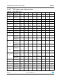
Contents
RM0031
Contents
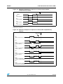
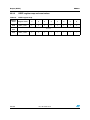
1
Central processing unit (CPU) . . . . . . . . . . . . . . . . . . . . . . . . . . . . . . . . 30
1.1
Introduction . . . . . . . . . . . . . . . . . . . . . . . . . . . . . . . . . . . . . . . . . . . . . . . 30
1.2
CPU registers . . . . . . . . . . . . . . . . . . . . . . . . . . . . . . . . . . . . . . . . . . . . . . 30
1.3
1.2.1
Description of CPU registers . . . . . . . . . . . . . . . . . . . . . . . . . . . . . . . . . 30
1.2.2
STM8 CPU register map . . . . . . . . . . . . . . . . . . . . . . . . . . . . . . . . . . . . 34
Global configuration register (CFG_GCR) . . . . . . . . . . . . . . . . . . . . . . . . 34
1.3.1
Activation level . . . . . . . . . . . . . . . . . . . . . . . . . . . . . . . . . . . . . . . . . . . . 34
1.3.2
SWIM disable . . . . . . . . . . . . . . . . . . . . . . . . . . . . . . . . . . . . . . . . . . . . . 35
1.3.3
Description of global configuration register (CFG_GCR) . . . . . . . . . . . . 35
1.3.4
Global configuration register map and reset values . . . . . . . . . . . . . . . . 35
2
Boot ROM . . . . . . . . . . . . . . . . . . . . . . . . . . . . . . . . . . . . . . . . . . . . . . . . . 36
3
Flash program memory and data EEPROM . . . . . . . . . . . . . . . . . . . . . 37
3.1
Introduction . . . . . . . . . . . . . . . . . . . . . . . . . . . . . . . . . . . . . . . . . . . . . . . 37
3.2
Glossary . . . . . . . . . . . . . . . . . . . . . . . . . . . . . . . . . . . . . . . . . . . . . . . . . . 37
3.3
Main Flash memory features . . . . . . . . . . . . . . . . . . . . . . . . . . . . . . . . . . 38
3.4
Memory organization . . . . . . . . . . . . . . . . . . . . . . . . . . . . . . . . . . . . . . . . 39
3.5
3.6
3.4.1
Low density device memory organization . . . . . . . . . . . . . . . . . . . . . . . 39
3.4.2
Medium density device memory organization . . . . . . . . . . . . . . . . . . . . 40
3.4.3
Medium+ density device memory organization . . . . . . . . . . . . . . . . . . . 41
3.4.4
High density device memory organization . . . . . . . . . . . . . . . . . . . . . . . 42
3.4.5
Proprietary code area (PCODE) . . . . . . . . . . . . . . . . . . . . . . . . . . . . . . 43
3.4.6
User boot area (UBC) . . . . . . . . . . . . . . . . . . . . . . . . . . . . . . . . . . . . . . 43
3.4.7
Data EEPROM (DATA) . . . . . . . . . . . . . . . . . . . . . . . . . . . . . . . . . . . . . . 46
3.4.8
Main program area . . . . . . . . . . . . . . . . . . . . . . . . . . . . . . . . . . . . . . . . 46
3.4.9
Option bytes . . . . . . . . . . . . . . . . . . . . . . . . . . . . . . . . . . . . . . . . . . . . . . 46
Memory protection . . . . . . . . . . . . . . . . . . . . . . . . . . . . . . . . . . . . . . . . . . 46
3.5.1
Readout protection . . . . . . . . . . . . . . . . . . . . . . . . . . . . . . . . . . . . . . . . 46
3.5.2
Memory access security system (MASS) . . . . . . . . . . . . . . . . . . . . . . . 47
3.5.3
Enabling write access to option bytes . . . . . . . . . . . . . . . . . . . . . . . . . . 48
Memory programming . . . . . . . . . . . . . . . . . . . . . . . . . . . . . . . . . . . . . . . 48
3.6.1
2/566
Read-while-write (RWW) . . . . . . . . . . . . . . . . . . . . . . . . . . . . . . . . . . . . 48
Doc ID 15226 Rev 8
RM0031
4
5
Contents
7
Byte programming . . . . . . . . . . . . . . . . . . . . . . . . . . . . . . . . . . . . . . . . . 49
3.6.3
Word programming . . . . . . . . . . . . . . . . . . . . . . . . . . . . . . . . . . . . . . . . 49
3.6.4
Block programming . . . . . . . . . . . . . . . . . . . . . . . . . . . . . . . . . . . . . . . . 50
3.6.5
Option byte programming . . . . . . . . . . . . . . . . . . . . . . . . . . . . . . . . . . . 51
3.7
Flash low power modes . . . . . . . . . . . . . . . . . . . . . . . . . . . . . . . . . . . . . . 52
3.8
ICP and IAP . . . . . . . . . . . . . . . . . . . . . . . . . . . . . . . . . . . . . . . . . . . . . . . 52
3.9
Flash registers . . . . . . . . . . . . . . . . . . . . . . . . . . . . . . . . . . . . . . . . . . . . . 57
3.9.1
Flash control register 1 (FLASH_CR1) . . . . . . . . . . . . . . . . . . . . . . . . . 57
3.9.2
Flash control register 2 (FLASH_CR2) . . . . . . . . . . . . . . . . . . . . . . . . . 57
3.9.3
Flash program memory unprotecting key register (FLASH_PUKR) . . . 58
3.9.4
Data EEPROM unprotection key register (FLASH_DUKR) . . . . . . . . . . 58
3.9.5
Flash status register (FLASH_IAPSR) . . . . . . . . . . . . . . . . . . . . . . . . . . 59
3.9.6
Flash register map and reset values . . . . . . . . . . . . . . . . . . . . . . . . . . . 60
Single wire interface module (SWIM) and debug module (DM) . . . . . 61
4.1
Introduction . . . . . . . . . . . . . . . . . . . . . . . . . . . . . . . . . . . . . . . . . . . . . . . 61
4.2
Main features . . . . . . . . . . . . . . . . . . . . . . . . . . . . . . . . . . . . . . . . . . . . . . 61
4.3
SWIM modes . . . . . . . . . . . . . . . . . . . . . . . . . . . . . . . . . . . . . . . . . . . . . . 61
Memory and register map . . . . . . . . . . . . . . . . . . . . . . . . . . . . . . . . . . . 62
5.1
6
3.6.2
Register description abbreviations . . . . . . . . . . . . . . . . . . . . . . . . . . . . . . 62
Power control (PWR) . . . . . . . . . . . . . . . . . . . . . . . . . . . . . . . . . . . . . . . . 63
6.1
Power supply . . . . . . . . . . . . . . . . . . . . . . . . . . . . . . . . . . . . . . . . . . . . . . 63
6.2
Power-on reset (POR)/power-down reset (PDR) . . . . . . . . . . . . . . . . . . . 64
6.3
Brownout reset (BOR) . . . . . . . . . . . . . . . . . . . . . . . . . . . . . . . . . . . . . . . 65
6.4
Programmable voltage detector (PVD) . . . . . . . . . . . . . . . . . . . . . . . . . . . 66
6.5
Internal voltage reference (VREFINT) . . . . . . . . . . . . . . . . . . . . . . . . . . . 67
6.6
Voltage regulator . . . . . . . . . . . . . . . . . . . . . . . . . . . . . . . . . . . . . . . . . . . 68
6.7
PWR registers . . . . . . . . . . . . . . . . . . . . . . . . . . . . . . . . . . . . . . . . . . . . . 69
6.7.1
Power control and status register 1 (PWR_CSR1) . . . . . . . . . . . . . . . . 69
6.7.2
PWR control and status register 2 (PWR_CSR2) . . . . . . . . . . . . . . . . . 70
6.7.3
PWR register map and reset values . . . . . . . . . . . . . . . . . . . . . . . . . . . 70
Low power modes . . . . . . . . . . . . . . . . . . . . . . . . . . . . . . . . . . . . . . . . . . 71
7.1
Slowing down the system clocks . . . . . . . . . . . . . . . . . . . . . . . . . . . . . . . 72
Doc ID 15226 Rev 8
3/566
Contents
RM0031
7.2
Peripheral clock gating (PCG) . . . . . . . . . . . . . . . . . . . . . . . . . . . . . . . . . 72
7.3
Wait mode (WFI or WFE mode) . . . . . . . . . . . . . . . . . . . . . . . . . . . . . . . . 72
7.4
Wait for interrupt (WFI) mode . . . . . . . . . . . . . . . . . . . . . . . . . . . . . . . . . . 73
7.5
Wait for event (WFE) mode . . . . . . . . . . . . . . . . . . . . . . . . . . . . . . . . . . . 73
7.6
WFE register map and reset values . . . . . . . . . . . . . . . . . . . . . . . . . . . . 79
Low power run mode . . . . . . . . . . . . . . . . . . . . . . . . . . . . . . . . . . . . . . . . 80
7.6.1
Entering Low power run mode . . . . . . . . . . . . . . . . . . . . . . . . . . . . . . . . 80
7.6.2
Exiting Low power run mode . . . . . . . . . . . . . . . . . . . . . . . . . . . . . . . . . 80
7.8
Halt mode . . . . . . . . . . . . . . . . . . . . . . . . . . . . . . . . . . . . . . . . . . . . . . . . . 81
7.8.1
Entering Halt mode . . . . . . . . . . . . . . . . . . . . . . . . . . . . . . . . . . . . . . . . 81
7.8.2
Exiting Halt mode . . . . . . . . . . . . . . . . . . . . . . . . . . . . . . . . . . . . . . . . . . 81
Active-halt mode . . . . . . . . . . . . . . . . . . . . . . . . . . . . . . . . . . . . . . . . . . . . 82
Reset (RST) . . . . . . . . . . . . . . . . . . . . . . . . . . . . . . . . . . . . . . . . . . . . . . . 83
8.1
“Reset state” and “under reset” definitions . . . . . . . . . . . . . . . . . . . . . . . . 83
8.2
External reset (NRST pin) . . . . . . . . . . . . . . . . . . . . . . . . . . . . . . . . . . . . 83
8.4
4/566
7.5.2
Low power wait mode . . . . . . . . . . . . . . . . . . . . . . . . . . . . . . . . . . . . . . . . 80
8.3
9
WFE registers . . . . . . . . . . . . . . . . . . . . . . . . . . . . . . . . . . . . . . . . . . . . 74
7.7
7.9
8
7.5.1
8.2.1
Asynchronous external reset description . . . . . . . . . . . . . . . . . . . . . . . . 83
8.2.2
Configuring NRST/PA1 pin as general purpose output . . . . . . . . . . . . . 84
Internal reset . . . . . . . . . . . . . . . . . . . . . . . . . . . . . . . . . . . . . . . . . . . . . . 84
8.3.1
Power-on reset (POR) . . . . . . . . . . . . . . . . . . . . . . . . . . . . . . . . . . . . . . 84
8.3.2
Independent watchdog reset . . . . . . . . . . . . . . . . . . . . . . . . . . . . . . . . . 84
8.3.3
Window watchdog reset . . . . . . . . . . . . . . . . . . . . . . . . . . . . . . . . . . . . . 84
8.3.4
SWIM reset . . . . . . . . . . . . . . . . . . . . . . . . . . . . . . . . . . . . . . . . . . . . . . 84
8.3.5
Illegal opcode reset . . . . . . . . . . . . . . . . . . . . . . . . . . . . . . . . . . . . . . . . 84
RST registers . . . . . . . . . . . . . . . . . . . . . . . . . . . . . . . . . . . . . . . . . . . . . . 85
8.4.1
Reset pin configuration register (RST_CR) . . . . . . . . . . . . . . . . . . . . . . 85
8.4.2
Reset status register (RST_SR) . . . . . . . . . . . . . . . . . . . . . . . . . . . . . . 85
8.4.3
RST register map and reset values . . . . . . . . . . . . . . . . . . . . . . . . . . . . 86
Clock control (CLK) . . . . . . . . . . . . . . . . . . . . . . . . . . . . . . . . . . . . . . . . . 87
9.1
Introduction . . . . . . . . . . . . . . . . . . . . . . . . . . . . . . . . . . . . . . . . . . . . . . . 87
9.2
HSE clock . . . . . . . . . . . . . . . . . . . . . . . . . . . . . . . . . . . . . . . . . . . . . . . . . 88
9.3
HSI clock . . . . . . . . . . . . . . . . . . . . . . . . . . . . . . . . . . . . . . . . . . . . . . . . . 90
Doc ID 15226 Rev 8
RM0031
Contents
9.4
LSE clock . . . . . . . . . . . . . . . . . . . . . . . . . . . . . . . . . . . . . . . . . . . . . . . . . 90
9.5
LSI clock . . . . . . . . . . . . . . . . . . . . . . . . . . . . . . . . . . . . . . . . . . . . . . . . . . 91
9.6
System clock sources . . . . . . . . . . . . . . . . . . . . . . . . . . . . . . . . . . . . . . . . 91
9.6.1
System startup . . . . . . . . . . . . . . . . . . . . . . . . . . . . . . . . . . . . . . . . . . . . 91
9.6.2
System clock switching procedures . . . . . . . . . . . . . . . . . . . . . . . . . . . . 92
9.7
Peripheral clock gating (PCG) . . . . . . . . . . . . . . . . . . . . . . . . . . . . . . . . . 95
9.8
Clock security system (CSS) . . . . . . . . . . . . . . . . . . . . . . . . . . . . . . . . . . 95
9.8.1
Clock security system on HSE . . . . . . . . . . . . . . . . . . . . . . . . . . . . . . . . 95
9.8.2
Clock security system on LSE . . . . . . . . . . . . . . . . . . . . . . . . . . . . . . . . 96
9.8.3
CSS on LSE control and status register (CSSLSE_CSR) . . . . . . . . . . . 97
9.8.4
CSS on LSE register map and reset values . . . . . . . . . . . . . . . . . . . . . 98
9.9
RTC and LCD clock . . . . . . . . . . . . . . . . . . . . . . . . . . . . . . . . . . . . . . . . . 98
9.10
BEEP clock . . . . . . . . . . . . . . . . . . . . . . . . . . . . . . . . . . . . . . . . . . . . . . . . 98
9.11
Configurable clock output capability (CCO) . . . . . . . . . . . . . . . . . . . . . . . 98
9.12
Clock-independent system clock sources for TIM2/TIM3 . . . . . . . . . . . . . 99
9.13
CLK interrupts . . . . . . . . . . . . . . . . . . . . . . . . . . . . . . . . . . . . . . . . . . . . . 99
9.14
CLK registers . . . . . . . . . . . . . . . . . . . . . . . . . . . . . . . . . . . . . . . . . . . . . 100
9.14.1
System clock divider register (CLK_CKDIVR) . . . . . . . . . . . . . . . . . . . 100
9.14.2
Clock RTC register (CLK_CRTCR) . . . . . . . . . . . . . . . . . . . . . . . . . . . 100
9.14.3
Internal clock register (CLK_ICKCR) . . . . . . . . . . . . . . . . . . . . . . . . . . 101
9.14.4
Peripheral clock gating register 1 (CLK_PCKENR1) . . . . . . . . . . . . . . 102
9.14.5
Peripheral clock gating register 2 (CLK_PCKENR2) . . . . . . . . . . . . . . 103
9.14.6
Peripheral clock gating register 3 (CLK_PCKENR3) . . . . . . . . . . . . . . 104
9.14.7
Configurable clock output register (CLK_CCOR) . . . . . . . . . . . . . . . . 105
9.14.8
External clock register (CLK_ECKCR) . . . . . . . . . . . . . . . . . . . . . . . . 106
9.14.9
System clock status register (CLK_SCSR) . . . . . . . . . . . . . . . . . . . . . 107
9.14.10 System clock switch register (CLK_SWR) . . . . . . . . . . . . . . . . . . . . . . 108
9.14.11 Switch control register (CLK_SWCR) . . . . . . . . . . . . . . . . . . . . . . . . . 108
9.14.12 Clock security system register (CLK_CSSR) . . . . . . . . . . . . . . . . . . . . 109
9.14.13 Clock BEEP register (CLK_CBEEPR) . . . . . . . . . . . . . . . . . . . . . . . . . 110
9.14.14 HSI calibration register (CLK_HSICALR) . . . . . . . . . . . . . . . . . . . . . . 110
9.14.15 HSI clock calibration trimming register (CLK_HSITRIMR) . . . . . . . . . . 111
9.14.16 HSI unlock register (CLK_HSIUNLCKR) . . . . . . . . . . . . . . . . . . . . . . . 111
9.14.17 Main regulator control status register (CLK_REGCSR) . . . . . . . . . . . . 112
9.14.18 CLK register map and reset values . . . . . . . . . . . . . . . . . . . . . . . . . . . 113
Doc ID 15226 Rev 8
5/566
Contents
10
RM0031
General purpose I/O ports (GPIO) . . . . . . . . . . . . . . . . . . . . . . . . . . . . 114
10.1
Introduction . . . . . . . . . . . . . . . . . . . . . . . . . . . . . . . . . . . . . . . . . . . . . . 114
10.2
GPIO main features . . . . . . . . . . . . . . . . . . . . . . . . . . . . . . . . . . . . . . . . 114
10.3
Port configuration and usage . . . . . . . . . . . . . . . . . . . . . . . . . . . . . . . . . 115
10.3.2
Output modes . . . . . . . . . . . . . . . . . . . . . . . . . . . . . . . . . . . . . . . . . . . 117
Reset configuration . . . . . . . . . . . . . . . . . . . . . . . . . . . . . . . . . . . . . . . . 117
10.5
Unused I/O pins . . . . . . . . . . . . . . . . . . . . . . . . . . . . . . . . . . . . . . . . . . . 117
10.6
Low power modes . . . . . . . . . . . . . . . . . . . . . . . . . . . . . . . . . . . . . . . . . 117
10.7
Input mode details . . . . . . . . . . . . . . . . . . . . . . . . . . . . . . . . . . . . . . . . . 117
10.9
10.7.1
Alternate function input . . . . . . . . . . . . . . . . . . . . . . . . . . . . . . . . . . . . 117
10.7.2
Interrupt capability . . . . . . . . . . . . . . . . . . . . . . . . . . . . . . . . . . . . . . . . 117
Output mode details . . . . . . . . . . . . . . . . . . . . . . . . . . . . . . . . . . . . . . . . 118
10.8.1
Alternate function output . . . . . . . . . . . . . . . . . . . . . . . . . . . . . . . . . . . 118
10.8.2
Slope control . . . . . . . . . . . . . . . . . . . . . . . . . . . . . . . . . . . . . . . . . . . . 118
GPIO registers . . . . . . . . . . . . . . . . . . . . . . . . . . . . . . . . . . . . . . . . . . . . 119
10.9.1
Port x output data register (Px_ODR) . . . . . . . . . . . . . . . . . . . . . . . . . 119
10.9.2
Port x pin input register (Px_IDR) . . . . . . . . . . . . . . . . . . . . . . . . . . . . 119
10.9.3
Port x data direction register (Px_DDR) . . . . . . . . . . . . . . . . . . . . . . . 120
10.9.4
Port x control register 1 (Px_CR1) . . . . . . . . . . . . . . . . . . . . . . . . . . . . 120
10.9.5
Port x control register 2 (Px_CR2) . . . . . . . . . . . . . . . . . . . . . . . . . . . . 121
10.9.6
Peripheral alternate function remapping . . . . . . . . . . . . . . . . . . . . . . . 121
10.9.7
GPIO register map and reset values . . . . . . . . . . . . . . . . . . . . . . . . . . 121
Routing interface (RI) and system configuration
controller (SYSCFG) . . . . . . . . . . . . . . . . . . . . . . . . . . . . . . . . . . . . . . . 122
11.1
Introduction . . . . . . . . . . . . . . . . . . . . . . . . . . . . . . . . . . . . . . . . . . . . . . 122
11.2
RI main features . . . . . . . . . . . . . . . . . . . . . . . . . . . . . . . . . . . . . . . . . . . 122
11.3
RI functional description . . . . . . . . . . . . . . . . . . . . . . . . . . . . . . . . . . . . . 124
11.4
6/566
Input modes . . . . . . . . . . . . . . . . . . . . . . . . . . . . . . . . . . . . . . . . . . . . . 116
10.4
10.8
11
10.3.1
11.3.1
I/O groups . . . . . . . . . . . . . . . . . . . . . . . . . . . . . . . . . . . . . . . . . . . . . . 124
11.3.2
TIM1 input capture routing . . . . . . . . . . . . . . . . . . . . . . . . . . . . . . . . . . 126
11.3.3
TIM2 & TIM3 routing . . . . . . . . . . . . . . . . . . . . . . . . . . . . . . . . . . . . . . 127
11.3.4
Comparator routing . . . . . . . . . . . . . . . . . . . . . . . . . . . . . . . . . . . . . . . 128
11.3.5
DAC routing . . . . . . . . . . . . . . . . . . . . . . . . . . . . . . . . . . . . . . . . . . . . . 128
11.3.6
Internal reference voltage routing . . . . . . . . . . . . . . . . . . . . . . . . . . . . 130
RI interrupts . . . . . . . . . . . . . . . . . . . . . . . . . . . . . . . . . . . . . . . . . . . . . . 130
Doc ID 15226 Rev 8
RM0031
Contents
11.5
RI registers . . . . . . . . . . . . . . . . . . . . . . . . . . . . . . . . . . . . . . . . . . . . . . . 130
11.5.1
Timer input capture routing register 1 (RI_ICR1) . . . . . . . . . . . . . . . . . 130
11.5.2
Timer input capture routing register 2 (RI_ICR2) . . . . . . . . . . . . . . . . . 131
11.5.3
I/O input register 1 (RI_IOIR1) . . . . . . . . . . . . . . . . . . . . . . . . . . . . . . . 131
11.5.4
I/O input register 2 (RI_IOIR2) . . . . . . . . . . . . . . . . . . . . . . . . . . . . . . . 131
11.5.5
I/O input register 3 (RI_IOIR3) . . . . . . . . . . . . . . . . . . . . . . . . . . . . . . . 132
11.5.6
I/O control mode register 1 (RI_IOCMR1) . . . . . . . . . . . . . . . . . . . . . . 132
11.5.7
I/O control mode register 2 (RI_IOCMR2) . . . . . . . . . . . . . . . . . . . . . . 132
11.5.8
I/O control mode register 3 (RI_IOCMR3) . . . . . . . . . . . . . . . . . . . . . . 133
11.5.9
I/O switch register 1 (RI_IOSR1) . . . . . . . . . . . . . . . . . . . . . . . . . . . . . 133
11.5.10 I/O switch register 2 (RI_IOSR2) . . . . . . . . . . . . . . . . . . . . . . . . . . . . . 134
11.5.11 I/O switch register 3 (RI_IOSR3) . . . . . . . . . . . . . . . . . . . . . . . . . . . . . 135
11.5.12 IO group control register (RI_IOGCR) . . . . . . . . . . . . . . . . . . . . . . . . . 136
11.5.13 Analog switch register 1 (RI_ASCR1) . . . . . . . . . . . . . . . . . . . . . . . . . 138
11.5.14 Analog switch register 2 (RI_ASCR2) . . . . . . . . . . . . . . . . . . . . . . . . . 139
11.5.15 Resistor control register (RI_RCR) . . . . . . . . . . . . . . . . . . . . . . . . . . . 140
11.5.16 Control register (RI_CR) . . . . . . . . . . . . . . . . . . . . . . . . . . . . . . . . . . . 140
11.5.17 IO mask register 1 (RI_IOMR1) . . . . . . . . . . . . . . . . . . . . . . . . . . . . . . 141
11.5.18 IO mask register 2 (RI_IOMR2) . . . . . . . . . . . . . . . . . . . . . . . . . . . . . . 141
11.5.19 IO mask register 3 (RI_IOMR3) . . . . . . . . . . . . . . . . . . . . . . . . . . . . . . 143
11.5.20 IO mask register 4 (RI_IOMR4) . . . . . . . . . . . . . . . . . . . . . . . . . . . . . . 143
11.5.21 I/O input register 4 (RI_IOIR4) . . . . . . . . . . . . . . . . . . . . . . . . . . . . . . . 144
11.5.22 I/O control mode register 4 (RI_IOCMR4) . . . . . . . . . . . . . . . . . . . . . . 144
11.5.23 I/O switch register 4 (RI_IOSR4) . . . . . . . . . . . . . . . . . . . . . . . . . . . . . 145
11.5.24 RI register map and reset values . . . . . . . . . . . . . . . . . . . . . . . . . . . . . 147
11.6
12
SYSCFG registers . . . . . . . . . . . . . . . . . . . . . . . . . . . . . . . . . . . . . . . . . 149
11.6.1
SYSCFG remap control register 1 (SYSCFG_RMPCR1) . . . . . . . . . . 149
11.6.2
SYSCFG remap control register 2 (SYSCFG_RMPCR2) . . . . . . . . . . 150
11.6.3
SYSCFG remap control register 3 (SYSCFG_RMPCR3) . . . . . . . . . . 151
11.6.4
SYSCFG register map and reset values . . . . . . . . . . . . . . . . . . . . . . . 152
Interrupt controller (ITC) . . . . . . . . . . . . . . . . . . . . . . . . . . . . . . . . . . . . 153
12.1
ITC introduction . . . . . . . . . . . . . . . . . . . . . . . . . . . . . . . . . . . . . . . . . . . 153
12.2
Interrupt masking and processing flow . . . . . . . . . . . . . . . . . . . . . . . . . . 153
12.3
12.2.1
Servicing pending interrupts . . . . . . . . . . . . . . . . . . . . . . . . . . . . . . . . 154
12.2.2
Interrupt sources . . . . . . . . . . . . . . . . . . . . . . . . . . . . . . . . . . . . . . . . . 155
Interrupts and low power modes . . . . . . . . . . . . . . . . . . . . . . . . . . . . . . 156
Doc ID 15226 Rev 8
7/566
Contents
RM0031
12.4
Activation level/low power mode control . . . . . . . . . . . . . . . . . . . . . . . . . 157
12.5
Concurrent and nested interrupt management . . . . . . . . . . . . . . . . . . . 157
12.5.1
Concurrent interrupt management mode . . . . . . . . . . . . . . . . . . . . . . . 157
12.5.2
Nested interrupt management mode . . . . . . . . . . . . . . . . . . . . . . . . . . 158
12.6
External interrupts . . . . . . . . . . . . . . . . . . . . . . . . . . . . . . . . . . . . . . . . . 159
12.7
Interrupt instructions . . . . . . . . . . . . . . . . . . . . . . . . . . . . . . . . . . . . . . . . 160
12.8
Interrupt mapping . . . . . . . . . . . . . . . . . . . . . . . . . . . . . . . . . . . . . . . . . . 160
12.9
ITC and EXTI registers . . . . . . . . . . . . . . . . . . . . . . . . . . . . . . . . . . . . . . 161
12.9.1
CPU condition code register interrupt bits (CCR) . . . . . . . . . . . . . . . . 161
12.9.2
Software priority register x (ITC_SPRx) . . . . . . . . . . . . . . . . . . . . . . . . 161
12.9.3
External interrupt control register 1 (EXTI_CR1) . . . . . . . . . . . . . . . . . 162
12.9.4
External interrupt control register 2 (EXTI_CR2) . . . . . . . . . . . . . . . . . 163
12.9.5
External interrupt control register 3 (EXTI_CR3) . . . . . . . . . . . . . . . . . 164
12.9.6
External interrupt control register 4 (EXTI_CR4) . . . . . . . . . . . . . . . . . 165
12.9.7
External interrupt status register 1 (EXTI_SR1) . . . . . . . . . . . . . . . . . 165
12.9.8
External interrupt status register 2 (EXTI_SR2) . . . . . . . . . . . . . . . . . 166
12.9.9
External interrupt port select register (EXTI_CONF1) . . . . . . . . . . . . . 167
12.9.10 External interrupt port select register (EXTI_CONF2) . . . . . . . . . . . . . 168
12.9.11 ITC and EXTI register map and reset values . . . . . . . . . . . . . . . . . . . . 169
13
Direct memory access controller (DMA) . . . . . . . . . . . . . . . . . . . . . . . 170
13.1
DMA introduction . . . . . . . . . . . . . . . . . . . . . . . . . . . . . . . . . . . . . . . . . . 170
Glossary . . . . . . . . . . . . . . . . . . . . . . . . . . . . . . . . . . . . . . . . . . . . . . . . . . . . . . . . 170
8/566
13.2
DMA main features . . . . . . . . . . . . . . . . . . . . . . . . . . . . . . . . . . . . . . . . . 171
13.3
DMA functional description . . . . . . . . . . . . . . . . . . . . . . . . . . . . . . . . . . 172
13.3.1
DMA transactions . . . . . . . . . . . . . . . . . . . . . . . . . . . . . . . . . . . . . . . . 172
13.3.2
DMA arbiter . . . . . . . . . . . . . . . . . . . . . . . . . . . . . . . . . . . . . . . . . . . . . 173
13.3.3
DMA channels . . . . . . . . . . . . . . . . . . . . . . . . . . . . . . . . . . . . . . . . . . . 173
13.3.4
DMA1 request mapping . . . . . . . . . . . . . . . . . . . . . . . . . . . . . . . . . . . . 180
13.3.5
DMA hardware request description . . . . . . . . . . . . . . . . . . . . . . . . . . . 182
13.4
DMA low power modes . . . . . . . . . . . . . . . . . . . . . . . . . . . . . . . . . . . . . 183
13.5
DMA interrupts . . . . . . . . . . . . . . . . . . . . . . . . . . . . . . . . . . . . . . . . . . . . 184
13.6
DMA registers . . . . . . . . . . . . . . . . . . . . . . . . . . . . . . . . . . . . . . . . . . . . . 184
13.6.1
DMA global configuration & status register (DMA_GCSR) . . . . . . . . . 184
13.6.2
DMA global interrupt register 1 (DMA_GIR1) . . . . . . . . . . . . . . . . . . . 185
13.6.3
DMA channel configuration register (DMA_CxCR) . . . . . . . . . . . . . . . 185
Doc ID 15226 Rev 8
RM0031
Contents
13.6.4
DMA channel status & priority register (DMA_CxSPR) . . . . . . . . . . . . 187
13.6.5
DMA number of data to transfer register (DMA_CxNDTR) . . . . . . . . . 188
13.6.6
DMA peripheral address high register (DMA_CxPARH) . . . . . . . . . . . 188
13.6.7
DMA peripheral address low register (DMA_CxPARL) . . . . . . . . . . . . 189
13.6.8
DMA channel 3 peripheral address high & memory 1 address high
register (DMA_C3PARH_C3M1ARH) . . . . . . . . . . . . . . . . . . . . . . . . . 189
13.6.9
DMA channel 3 peripheral address low & memory 1 address low
register (DMA_C3PARL_C3M1ARL) . . . . . . . . . . . . . . . . . . . . . . . . . . 190
13.6.10 DMA memory 0 address high register (DMA_CxM0ARH) . . . . . . . . . . 190
13.6.11 DMA memory 0 address low register (DMA_CxM0ARL) . . . . . . . . . . . 191
13.6.12 DMA channel 3 memory 0 extended address register
(DMA_C3M0EAR) . . . . . . . . . . . . . . . . . . . . . . . . . . . . . . . . . . . . . . . . 191
13.6.13 DMA register map and reset values . . . . . . . . . . . . . . . . . . . . . . . . . . . 192
14
Analog-to-digital converter (ADC) . . . . . . . . . . . . . . . . . . . . . . . . . . . . 194
14.1
ADC introduction . . . . . . . . . . . . . . . . . . . . . . . . . . . . . . . . . . . . . . . . . . 194
14.2
ADC main features . . . . . . . . . . . . . . . . . . . . . . . . . . . . . . . . . . . . . . . . . 194
14.3
ADC functional description . . . . . . . . . . . . . . . . . . . . . . . . . . . . . . . . . . . 195
14.3.1
General description . . . . . . . . . . . . . . . . . . . . . . . . . . . . . . . . . . . . . . . 195
14.3.2
Number of analog channels . . . . . . . . . . . . . . . . . . . . . . . . . . . . . . . . . 196
14.3.3
ADC on-off control . . . . . . . . . . . . . . . . . . . . . . . . . . . . . . . . . . . . . . . . 196
14.3.4
Single conversion mode . . . . . . . . . . . . . . . . . . . . . . . . . . . . . . . . . . . . 196
14.3.5
Continuous conversion mode . . . . . . . . . . . . . . . . . . . . . . . . . . . . . . . 198
14.3.6
ADC clock . . . . . . . . . . . . . . . . . . . . . . . . . . . . . . . . . . . . . . . . . . . . . . 198
14.3.7
Analog watchdog . . . . . . . . . . . . . . . . . . . . . . . . . . . . . . . . . . . . . . . . . 198
14.3.8
Interrupts . . . . . . . . . . . . . . . . . . . . . . . . . . . . . . . . . . . . . . . . . . . . . . . 199
14.3.9
Channel selection (Scan mode) . . . . . . . . . . . . . . . . . . . . . . . . . . . . . . 199
14.3.10 Data integrity . . . . . . . . . . . . . . . . . . . . . . . . . . . . . . . . . . . . . . . . . . . . 200
14.3.11 DMA transfer . . . . . . . . . . . . . . . . . . . . . . . . . . . . . . . . . . . . . . . . . . . . 200
14.3.12 Configurable resolution . . . . . . . . . . . . . . . . . . . . . . . . . . . . . . . . . . . . 200
14.3.13 Data alignment . . . . . . . . . . . . . . . . . . . . . . . . . . . . . . . . . . . . . . . . . . . 200
14.3.14 Programmable sampling time . . . . . . . . . . . . . . . . . . . . . . . . . . . . . . . 201
14.3.15 Schmitt trigger disabling . . . . . . . . . . . . . . . . . . . . . . . . . . . . . . . . . . . 202
14.3.16 Temperature sensor . . . . . . . . . . . . . . . . . . . . . . . . . . . . . . . . . . . . . . . 202
14.3.17 Internal reference voltage conversion . . . . . . . . . . . . . . . . . . . . . . . . . 203
14.4
ADC low power modes . . . . . . . . . . . . . . . . . . . . . . . . . . . . . . . . . . . . . . 203
14.5
ADC interrupts . . . . . . . . . . . . . . . . . . . . . . . . . . . . . . . . . . . . . . . . . . . . 203
Doc ID 15226 Rev 8
9/566
Contents
RM0031
14.6
ADC registers . . . . . . . . . . . . . . . . . . . . . . . . . . . . . . . . . . . . . . . . . . . . . 204
14.6.1
ADC configuration register 1 (ADC_CR1) . . . . . . . . . . . . . . . . . . . . . . 204
14.6.2
ADC configuration register 2 (ADC_CR2) . . . . . . . . . . . . . . . . . . . . . . 205
14.6.3
ADC configuration register 3 (ADC_CR3) . . . . . . . . . . . . . . . . . . . . . . 205
14.6.4
ADC status register (ADC_SR) . . . . . . . . . . . . . . . . . . . . . . . . . . . . . . 207
14.6.5
ADC data register high (ADC_DRH) . . . . . . . . . . . . . . . . . . . . . . . . . . 208
14.6.6
ADC data register low (ADC_DRL) . . . . . . . . . . . . . . . . . . . . . . . . . . . 208
14.6.7
ADC high threshold register high (ADC_HTRH) . . . . . . . . . . . . . . . . . 209
14.6.8
ADC high threshold register low (ADC_HTRL) . . . . . . . . . . . . . . . . . . 209
14.6.9
ADC low threshold register high (ADC_LTRH) . . . . . . . . . . . . . . . . . . 209
14.6.10 ADC low threshold register low (ADC_LTRL) . . . . . . . . . . . . . . . . . . . 210
14.6.11 ADC channel sequence 1 register (ADC_SQR1) . . . . . . . . . . . . . . . . 210
14.6.12 ADC channel sequence register 2 (ADC_SQR2) . . . . . . . . . . . . . . . . 211
14.6.13 ADC channel select scan 3 (ADC_SQR3) . . . . . . . . . . . . . . . . . . . . . . 211
14.6.14 ADC channel select scan 4 (ADC_SQR4) . . . . . . . . . . . . . . . . . . . . . . 212
14.6.15 ADC trigger disable 1 (ADC_TRIGR1) . . . . . . . . . . . . . . . . . . . . . . . . 212
14.6.16 ADC trigger disable 2 (ADC_TRIGR2) . . . . . . . . . . . . . . . . . . . . . . . . 213
14.6.17 ADC trigger disable 3 (ADC_TRIGR3) . . . . . . . . . . . . . . . . . . . . . . . . 213
14.6.18 ADC trigger disable 4 (ADC_TRIGR4) . . . . . . . . . . . . . . . . . . . . . . . . 213
14.6.19 ADC register map and reset values . . . . . . . . . . . . . . . . . . . . . . . . . . . 214
15
Digital-to-analog converter (DAC) . . . . . . . . . . . . . . . . . . . . . . . . . . . . 215
15.1
DAC introduction . . . . . . . . . . . . . . . . . . . . . . . . . . . . . . . . . . . . . . . . . . 215
15.2
DAC main features . . . . . . . . . . . . . . . . . . . . . . . . . . . . . . . . . . . . . . . . . 215
15.3
DAC functional description . . . . . . . . . . . . . . . . . . . . . . . . . . . . . . . . . . . 217
15.3.1
DAC channel x enable . . . . . . . . . . . . . . . . . . . . . . . . . . . . . . . . . . . . . 217
15.3.2
DAC output buffer enable . . . . . . . . . . . . . . . . . . . . . . . . . . . . . . . . . . . 217
15.3.3
DAC output switch configuration . . . . . . . . . . . . . . . . . . . . . . . . . . . . . 217
15.3.4
DAC data format . . . . . . . . . . . . . . . . . . . . . . . . . . . . . . . . . . . . . . . . . 218
15.3.5
DAC conversion sequence . . . . . . . . . . . . . . . . . . . . . . . . . . . . . . . . . . 218
15.3.6
DAC output voltage . . . . . . . . . . . . . . . . . . . . . . . . . . . . . . . . . . . . . . . 218
15.3.7
DAC trigger selection . . . . . . . . . . . . . . . . . . . . . . . . . . . . . . . . . . . . . . 218
15.3.8
DAC DMA request . . . . . . . . . . . . . . . . . . . . . . . . . . . . . . . . . . . . . . . . 219
15.3.9
DAC DMA underrun interrupt . . . . . . . . . . . . . . . . . . . . . . . . . . . . . . . . 219
15.3.10 Noise generation . . . . . . . . . . . . . . . . . . . . . . . . . . . . . . . . . . . . . . . . . 219
15.3.11 Triangle-wave generation . . . . . . . . . . . . . . . . . . . . . . . . . . . . . . . . . . . 220
15.3.12 Dual DAC conversion . . . . . . . . . . . . . . . . . . . . . . . . . . . . . . . . . . . . . . 221
10/566
Doc ID 15226 Rev 8
RM0031
Contents
15.4
DAC registers . . . . . . . . . . . . . . . . . . . . . . . . . . . . . . . . . . . . . . . . . . . . . 225
15.4.1
DAC channel x control register 1 (DAC_CHxCR1) . . . . . . . . . . . . . . . 225
15.4.2
DAC channel x control register 2 (DAC_CHxCR2) . . . . . . . . . . . . . . . 226
15.4.3
DAC software trigger register (DAC_SWTRIGR) . . . . . . . . . . . . . . . . . 227
15.4.4
DAC status register (DAC_SR) . . . . . . . . . . . . . . . . . . . . . . . . . . . . . . 227
15.4.5
DAC channel x right aligned data holding register high
(DAC_RDHRH) . . . . . . . . . . . . . . . . . . . . . . . . . . . . . . . . . . . . . . . . . . 228
15.4.6
DAC channel x right aligned data holding register low
(DAC_CHxRDHRL) . . . . . . . . . . . . . . . . . . . . . . . . . . . . . . . . . . . . . . . 228
15.4.7
DAC channel x left aligned data holding register high
(DAC_CHxLDHRH) . . . . . . . . . . . . . . . . . . . . . . . . . . . . . . . . . . . . . . . 228
15.4.8
DAC channel x left aligned data holding register low
(DAC_CHxLDHRL) . . . . . . . . . . . . . . . . . . . . . . . . . . . . . . . . . . . . . . . 229
15.4.9
DAC channel x 8-bit data holding register
(DAC_CHxDHR8) . . . . . . . . . . . . . . . . . . . . . . . . . . . . . . . . . . . . . . . . 229
15.4.10 DAC channel x dual mode right aligned data holding register high
(DAC_DCHxRDHRH) . . . . . . . . . . . . . . . . . . . . . . . . . . . . . . . . . . . . . 230
15.4.11 DAC channel x dual mode right aligned data holding register low
(DAC_DCHxRDHRL) . . . . . . . . . . . . . . . . . . . . . . . . . . . . . . . . . . . . . . 230
15.4.12 DAC channel x dual mode left aligned data holding register high
(DAC_DCHxLDHRH) . . . . . . . . . . . . . . . . . . . . . . . . . . . . . . . . . . . . . . 231
15.4.13 DAC channel x left aligned data holding register low
(DAC_DCHxLDHRL) . . . . . . . . . . . . . . . . . . . . . . . . . . . . . . . . . . . . . . 231
15.4.14 DAC channel x dual mode 8-bit data holding register
(DAC_DCHxDHR8) . . . . . . . . . . . . . . . . . . . . . . . . . . . . . . . . . . . . . . . 232
15.4.15 DAC channel x data output register high
(DAC_CHxDORH) . . . . . . . . . . . . . . . . . . . . . . . . . . . . . . . . . . . . . . . . 232
15.4.16 DAC channel x data output register low
(DAC_CHxDORL) . . . . . . . . . . . . . . . . . . . . . . . . . . . . . . . . . . . . . . . . 232
15.4.17 DAC register map and reset values . . . . . . . . . . . . . . . . . . . . . . . . . . . 233
16
Comparators (COMP) . . . . . . . . . . . . . . . . . . . . . . . . . . . . . . . . . . . . . . 236
16.1
COMP introduction . . . . . . . . . . . . . . . . . . . . . . . . . . . . . . . . . . . . . . . . . 236
16.2
COMP main features . . . . . . . . . . . . . . . . . . . . . . . . . . . . . . . . . . . . . . . 238
16.3
Comparator 1 (COMP1) . . . . . . . . . . . . . . . . . . . . . . . . . . . . . . . . . . . . . 239
16.4
Comparator 2 (COMP2) . . . . . . . . . . . . . . . . . . . . . . . . . . . . . . . . . . . . . 240
16.5
Using the comparators in window mode . . . . . . . . . . . . . . . . . . . . . . . . 241
16.6
COMP low power modes . . . . . . . . . . . . . . . . . . . . . . . . . . . . . . . . . . . . 242
16.7
COMP interrupts . . . . . . . . . . . . . . . . . . . . . . . . . . . . . . . . . . . . . . . . . . 242
16.8
COMP registers . . . . . . . . . . . . . . . . . . . . . . . . . . . . . . . . . . . . . . . . . . . 243
Doc ID 15226 Rev 8
11/566
Contents
17
RM0031
16.8.1
Comparator control and status register 1 (COMP_CSR1) . . . . . . . . . . 243
16.8.2
Comparator control and status register 2 (COMP_CSR2) . . . . . . . . . . 244
16.8.3
Comparator control and status register 3 (COMP_CSR3) . . . . . . . . . . 245
16.8.4
Comparator control and status register 4 (COMP_CSR4) . . . . . . . . . . 246
16.8.5
Comparator control and status register 5 (COMP_CSR5) . . . . . . . . . . 246
16.8.6
COMP register map and reset values . . . . . . . . . . . . . . . . . . . . . . . . . 247
LCD controller . . . . . . . . . . . . . . . . . . . . . . . . . . . . . . . . . . . . . . . . . . . . 248
17.1
LCD controller introduction . . . . . . . . . . . . . . . . . . . . . . . . . . . . . . . . . . . 248
17.1.1
18
12/566
Definitions . . . . . . . . . . . . . . . . . . . . . . . . . . . . . . . . . . . . . . . . . . . . . . 248
17.2
LCD controller main features . . . . . . . . . . . . . . . . . . . . . . . . . . . . . . . . . 249
17.3
LCD functional description . . . . . . . . . . . . . . . . . . . . . . . . . . . . . . . . . . . 250
17.3.1
General description . . . . . . . . . . . . . . . . . . . . . . . . . . . . . . . . . . . . . . . 250
17.3.2
Frequency generator . . . . . . . . . . . . . . . . . . . . . . . . . . . . . . . . . . . . . . 251
17.3.3
Common driver . . . . . . . . . . . . . . . . . . . . . . . . . . . . . . . . . . . . . . . . . . 254
17.3.4
Segment driver . . . . . . . . . . . . . . . . . . . . . . . . . . . . . . . . . . . . . . . . . . 262
17.3.5
Enabling a segment . . . . . . . . . . . . . . . . . . . . . . . . . . . . . . . . . . . . . . . 263
17.3.6
Blink . . . . . . . . . . . . . . . . . . . . . . . . . . . . . . . . . . . . . . . . . . . . . . . . . . . 263
17.3.7
Multiplexing COM[7:4] and SEG[43:40], SEG[39:36], or SEG[31:28] . 263
17.3.8
Generation of LCD voltage levels . . . . . . . . . . . . . . . . . . . . . . . . . . . . 264
17.4
LCD controller low power modes . . . . . . . . . . . . . . . . . . . . . . . . . . . . . . 266
17.5
LCD controller interrupts . . . . . . . . . . . . . . . . . . . . . . . . . . . . . . . . . . . . 266
17.6
LCD controller registers . . . . . . . . . . . . . . . . . . . . . . . . . . . . . . . . . . . . . 267
17.6.1
Control register 1 (LCD_CR1) . . . . . . . . . . . . . . . . . . . . . . . . . . . . . . . 267
17.6.2
Control register 2 (LCD_CR2) . . . . . . . . . . . . . . . . . . . . . . . . . . . . . . . 268
17.6.3
Control register 3 (LCD_CR3) . . . . . . . . . . . . . . . . . . . . . . . . . . . . . . . 269
17.6.4
Frequency selection register (LCD_FRQ) . . . . . . . . . . . . . . . . . . . . . . 270
17.6.5
Port mask registers (LCD_PM) . . . . . . . . . . . . . . . . . . . . . . . . . . . . . . 270
17.6.6
Control register 4 (LCD_CR4) . . . . . . . . . . . . . . . . . . . . . . . . . . . . . . . 271
17.6.7
LCD display memory (LCD_RAM) . . . . . . . . . . . . . . . . . . . . . . . . . . . . 272
17.6.8
LCD register map and reset values . . . . . . . . . . . . . . . . . . . . . . . . . . . 274
Timer overview . . . . . . . . . . . . . . . . . . . . . . . . . . . . . . . . . . . . . . . . . . . 276
18.1
Timer feature comparison . . . . . . . . . . . . . . . . . . . . . . . . . . . . . . . . . . . 277
18.2
Glossary of timer signal names . . . . . . . . . . . . . . . . . . . . . . . . . . . . . . . 277
Doc ID 15226 Rev 8
RM0031
19
Contents
16-bit advanced control timer (TIM1) . . . . . . . . . . . . . . . . . . . . . . . . . . 279
19.1
Introduction . . . . . . . . . . . . . . . . . . . . . . . . . . . . . . . . . . . . . . . . . . . . . . 279
19.2
TIM1 main features . . . . . . . . . . . . . . . . . . . . . . . . . . . . . . . . . . . . . . . . 280
19.3
TIM1 time base unit . . . . . . . . . . . . . . . . . . . . . . . . . . . . . . . . . . . . . . . . 282
19.4
19.5
19.3.1
Reading and writing to the 16-bit counter . . . . . . . . . . . . . . . . . . . . . . 283
19.3.2
Write sequence for 16-bit TIM1_ARR register . . . . . . . . . . . . . . . . . . . 283
19.3.3
Prescaler . . . . . . . . . . . . . . . . . . . . . . . . . . . . . . . . . . . . . . . . . . . . . . . 283
19.3.4
Up-counting mode . . . . . . . . . . . . . . . . . . . . . . . . . . . . . . . . . . . . . . . . 284
19.3.5
Down-counting mode . . . . . . . . . . . . . . . . . . . . . . . . . . . . . . . . . . . . . . 286
19.3.6
Center-aligned mode (up/down counting) . . . . . . . . . . . . . . . . . . . . . . 288
19.3.7
Repetition down-counter . . . . . . . . . . . . . . . . . . . . . . . . . . . . . . . . . . . 290
TIM1 clock/trigger controller . . . . . . . . . . . . . . . . . . . . . . . . . . . . . . . . . . 292
19.4.1
Prescaler clock (CK_PSC) . . . . . . . . . . . . . . . . . . . . . . . . . . . . . . . . . . 292
19.4.2
Internal clock source (fSYSCLK) . . . . . . . . . . . . . . . . . . . . . . . . . . . . . 293
19.4.3
External clock source mode 1 . . . . . . . . . . . . . . . . . . . . . . . . . . . . . . . 293
19.4.4
External clock source mode 2 . . . . . . . . . . . . . . . . . . . . . . . . . . . . . . . 295
19.4.5
Trigger synchronization . . . . . . . . . . . . . . . . . . . . . . . . . . . . . . . . . . . . 296
19.4.6
Synchronization between timers . . . . . . . . . . . . . . . . . . . . . . . . . . . . . 300
TIM1 capture/compare channels . . . . . . . . . . . . . . . . . . . . . . . . . . . . . . 306
19.5.1
Write sequence for 16-bit TIM1_CCRi registers . . . . . . . . . . . . . . . . . 307
19.5.2
Input stage . . . . . . . . . . . . . . . . . . . . . . . . . . . . . . . . . . . . . . . . . . . . . . 308
19.5.3
Input capture mode . . . . . . . . . . . . . . . . . . . . . . . . . . . . . . . . . . . . . . . 309
19.5.4
Output stage . . . . . . . . . . . . . . . . . . . . . . . . . . . . . . . . . . . . . . . . . . . . 311
19.5.5
Forced output mode . . . . . . . . . . . . . . . . . . . . . . . . . . . . . . . . . . . . . . . 312
19.5.6
Output compare mode . . . . . . . . . . . . . . . . . . . . . . . . . . . . . . . . . . . . . 312
19.5.7
PWM mode . . . . . . . . . . . . . . . . . . . . . . . . . . . . . . . . . . . . . . . . . . . . . 314
19.5.8
Using the break function . . . . . . . . . . . . . . . . . . . . . . . . . . . . . . . . . . . 321
19.5.9
Clearing the OCiREF signal on an external event . . . . . . . . . . . . . . . . 324
19.5.10 Encoder interface mode . . . . . . . . . . . . . . . . . . . . . . . . . . . . . . . . . . . . 325
19.5.11 Timer input XOR function . . . . . . . . . . . . . . . . . . . . . . . . . . . . . . . . . . 327
19.5.12 Interfacing with Hall sensors . . . . . . . . . . . . . . . . . . . . . . . . . . . . . . . . 327
19.6
TIM1 interrupts . . . . . . . . . . . . . . . . . . . . . . . . . . . . . . . . . . . . . . . . . . . . 329
19.6.1
19.7
TIM1 wait-for-event capability . . . . . . . . . . . . . . . . . . . . . . . . . . . . . . . 329
TIM1 DMA . . . . . . . . . . . . . . . . . . . . . . . . . . . . . . . . . . . . . . . . . . . . . . . 329
19.7.1
DMA single mode . . . . . . . . . . . . . . . . . . . . . . . . . . . . . . . . . . . . . . . . 329
19.7.2
DMA burst mode . . . . . . . . . . . . . . . . . . . . . . . . . . . . . . . . . . . . . . . . . 330
Doc ID 15226 Rev 8
13/566
Contents
RM0031
19.8
TIM1 registers . . . . . . . . . . . . . . . . . . . . . . . . . . . . . . . . . . . . . . . . . . . . 331
19.8.1
Control register 1 (TIM1_CR1) . . . . . . . . . . . . . . . . . . . . . . . . . . . . . . 331
19.8.2
Control register 2 (TIM1_CR2) . . . . . . . . . . . . . . . . . . . . . . . . . . . . . . 333
19.8.3
Slave mode control register (TIM1_SMCR) . . . . . . . . . . . . . . . . . . . . . 334
19.8.4
External trigger register (TIM1_ETR) . . . . . . . . . . . . . . . . . . . . . . . . . . 335
19.8.5
DMA request enable register (TIM1_DER) . . . . . . . . . . . . . . . . . . . . . 337
19.8.6
Interrupt enable register (TIM1_IER) . . . . . . . . . . . . . . . . . . . . . . . . . . 338
19.8.7
Status register 1 (TIM1_SR1) . . . . . . . . . . . . . . . . . . . . . . . . . . . . . . . 339
19.8.8
Status register 2 (TIM1_SR2) . . . . . . . . . . . . . . . . . . . . . . . . . . . . . . . 340
19.8.9
Event generation register (TIM1_EGR) . . . . . . . . . . . . . . . . . . . . . . . . 341
19.8.10 Capture/compare mode register 1 (TIM1_CCMR1) . . . . . . . . . . . . . . . 342
19.8.11 Capture/compare mode register 2 (TIM1_CCMR2) . . . . . . . . . . . . . . . 345
19.8.12 Capture/compare mode register 3 (TIM1_CCMR3) . . . . . . . . . . . . . . . 346
19.8.13 Capture/compare mode register 4 (TIM1_CCMR4) . . . . . . . . . . . . . . . 347
19.8.14 Capture/compare enable register 1 (TIM1_CCER1) . . . . . . . . . . . . . . 348
19.8.15 Capture/compare enable register 2 (TIM1_CCER2) . . . . . . . . . . . . . . 351
19.8.16 Counter high (TIM1_CNTRH) . . . . . . . . . . . . . . . . . . . . . . . . . . . . . . . 351
19.8.17 Counter low (TIM1_CNTRL) . . . . . . . . . . . . . . . . . . . . . . . . . . . . . . . . 352
19.8.18 Prescaler high (TIM1_PSCRH) . . . . . . . . . . . . . . . . . . . . . . . . . . . . . . 352
19.8.19 Prescaler low (TIM1_PSCRL) . . . . . . . . . . . . . . . . . . . . . . . . . . . . . . . 352
19.8.20 Auto-reload register high (TIM1_ARRH) . . . . . . . . . . . . . . . . . . . . . . . 353
19.8.21 Auto-reload register low (TIM1_ARRL) . . . . . . . . . . . . . . . . . . . . . . . . 353
19.8.22 Repetition counter register (TIM1_RCR) . . . . . . . . . . . . . . . . . . . . . . . 353
19.8.23 Capture/compare register 1 high (TIM1_CCR1H) . . . . . . . . . . . . . . . . 354
19.8.24 Capture/compare register 1 low (TIM1_CCR1L) . . . . . . . . . . . . . . . . . 354
19.8.25 Capture/compare register 2 high (TIM1_CCR2H) . . . . . . . . . . . . . . . . 355
19.8.26 Capture/compare register 2 low (TIM1_CCR2L) . . . . . . . . . . . . . . . . . 355
19.8.27 Capture/compare register 3 high (TIM1_CCR3H) . . . . . . . . . . . . . . . . 356
19.8.28 Capture/compare register 3 low (TIM1_CCR3L) . . . . . . . . . . . . . . . . . 356
19.8.29 Capture/compare register 4 high (TIM1_CCR4H) . . . . . . . . . . . . . . . . 357
19.8.30 Capture/compare register 4 low (TIM1_CCR4L) . . . . . . . . . . . . . . . . . 357
19.8.31 Break register (TIM1_BKR) . . . . . . . . . . . . . . . . . . . . . . . . . . . . . . . . . 358
19.8.32 Deadtime register (TIM1_DTR) . . . . . . . . . . . . . . . . . . . . . . . . . . . . . . 359
19.8.33 Output idle state register (TIM1_OISR) . . . . . . . . . . . . . . . . . . . . . . . . 360
19.8.34 DMA control register 1 (TIM1_DCR1) . . . . . . . . . . . . . . . . . . . . . . . . . 360
19.8.35 DMA control register 2 (TIM1_DCR2) . . . . . . . . . . . . . . . . . . . . . . . . . 361
19.8.36 DMA address for burst mode (TIM1_DMAR) . . . . . . . . . . . . . . . . . . . . 361
14/566
Doc ID 15226 Rev 8
RM0031
Contents
19.8.37 TIM1 register map and reset values . . . . . . . . . . . . . . . . . . . . . . . . . . 362
20
16-bit general purpose timers (TIM2, TIM3, TIM5) . . . . . . . . . . . . . . . 364
20.1
Introduction . . . . . . . . . . . . . . . . . . . . . . . . . . . . . . . . . . . . . . . . . . . . . . 364
20.2
TIMx main features . . . . . . . . . . . . . . . . . . . . . . . . . . . . . . . . . . . . . . . . . 364
20.3
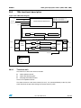
TIMx functional description . . . . . . . . . . . . . . . . . . . . . . . . . . . . . . . . . . 365
20.3.1
Time base unit . . . . . . . . . . . . . . . . . . . . . . . . . . . . . . . . . . . . . . . . . . . 365
20.3.2
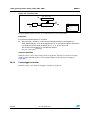
Clock/trigger controller . . . . . . . . . . . . . . . . . . . . . . . . . . . . . . . . . . . . . 366
20.3.3
Capture/compare channels . . . . . . . . . . . . . . . . . . . . . . . . . . . . . . . . . 367
20.3.4
Timer input XOR function . . . . . . . . . . . . . . . . . . . . . . . . . . . . . . . . . . 369
20.4
TIMx interrupts . . . . . . . . . . . . . . . . . . . . . . . . . . . . . . . . . . . . . . . . . . . . 369
20.5
TIMx registers . . . . . . . . . . . . . . . . . . . . . . . . . . . . . . . . . . . . . . . . . . . . . 370
20.5.1
Control register 1 (TIMx_CR1) . . . . . . . . . . . . . . . . . . . . . . . . . . . . . . . 370
20.5.2
Control register 2 (TIMx_CR2) . . . . . . . . . . . . . . . . . . . . . . . . . . . . . . . 371
20.5.3
Slave mode control register (TIMx_SMCR) . . . . . . . . . . . . . . . . . . . . . 372
20.5.4
External trigger register (TIMx_ETR) . . . . . . . . . . . . . . . . . . . . . . . . . . 373
20.5.5
DMA request enable register (TIMx_DER) . . . . . . . . . . . . . . . . . . . . . 374
20.5.6
Interrupt enable register (TIMx_IER) . . . . . . . . . . . . . . . . . . . . . . . . . . 375
20.5.7
Status register 1 (TIMx_SR1) . . . . . . . . . . . . . . . . . . . . . . . . . . . . . . . 376
20.5.8
Status register 2 (TIMx_SR2) . . . . . . . . . . . . . . . . . . . . . . . . . . . . . . . 377
20.5.9
Event generation register (TIMx_EGR) . . . . . . . . . . . . . . . . . . . . . . . . 378
20.5.10 Capture/compare mode register 1 (TIMx_CCMR1) . . . . . . . . . . . . . . . 379
20.5.11 Capture/compare mode register 2 (TIMx_CCMR2) . . . . . . . . . . . . . . . 381
20.5.12 Capture/compare enable register 1 (TIMx_CCER1) . . . . . . . . . . . . . . 382
20.5.13 Counter high (TIMx_CNTRH) . . . . . . . . . . . . . . . . . . . . . . . . . . . . . . . 383
20.5.14 Counter low (TIMx_CNTRL) . . . . . . . . . . . . . . . . . . . . . . . . . . . . . . . . 384
20.5.15 Prescaler register (TIMx_PSCR) . . . . . . . . . . . . . . . . . . . . . . . . . . . . . 384
20.5.16 Auto-reload register high (TIMx_ARRH) . . . . . . . . . . . . . . . . . . . . . . . 384
20.5.17 Auto-reload register low (TIMx_ARRL) . . . . . . . . . . . . . . . . . . . . . . . . 385
20.5.18 Capture/compare register 1 high (TIMx_CCR1H) . . . . . . . . . . . . . . . . 385
20.5.19 Capture/compare register 1 low (TIMx_CCR1L) . . . . . . . . . . . . . . . . . 386
20.5.20 Capture/compare register 2 high (TIMx_CCR2H) . . . . . . . . . . . . . . . . 386
20.5.21 Capture/compare register 2 low (TIMx_CCR2L) . . . . . . . . . . . . . . . . . 386
20.5.22 Break register (TIMx_BKR) . . . . . . . . . . . . . . . . . . . . . . . . . . . . . . . . . 387
20.5.23 Output idle state register (TIMx_OISR) . . . . . . . . . . . . . . . . . . . . . . . . 389
20.5.24 TIMx register map and reset values . . . . . . . . . . . . . . . . . . . . . . . . . . . 389
Doc ID 15226 Rev 8
15/566
Contents
21
RM0031
8-bit basic timer (TIM4) . . . . . . . . . . . . . . . . . . . . . . . . . . . . . . . . . . . . . 391
21.1
Introduction . . . . . . . . . . . . . . . . . . . . . . . . . . . . . . . . . . . . . . . . . . . . . . 391
21.2
TIM4 main features . . . . . . . . . . . . . . . . . . . . . . . . . . . . . . . . . . . . . . . . 391
21.3
TIM4interrupts . . . . . . . . . . . . . . . . . . . . . . . . . . . . . . . . . . . . . . . . . . . . 391
21.4
TIM4 clock selection . . . . . . . . . . . . . . . . . . . . . . . . . . . . . . . . . . . . . . . . 392
21.5
TIM4 registers . . . . . . . . . . . . . . . . . . . . . . . . . . . . . . . . . . . . . . . . . . . . 392
21.5.1
Control register 1 (TIM4_CR1) . . . . . . . . . . . . . . . . . . . . . . . . . . . . . . 392
21.5.2
Control register 2 (TIM4_CR2) . . . . . . . . . . . . . . . . . . . . . . . . . . . . . . 393
21.5.3
Slave mode control register (TIM4_SMCR) . . . . . . . . . . . . . . . . . . . . . 393
21.5.4
DMA request enable register (TIM4_DER) . . . . . . . . . . . . . . . . . . . . . 395
21.5.5
Interrupt enable register (TIM4_IER) . . . . . . . . . . . . . . . . . . . . . . . . . . 395
21.5.6
Status register 1 (TIM4_SR) . . . . . . . . . . . . . . . . . . . . . . . . . . . . . . . . 395
21.5.7
Event generation register (TIM4_EGR) . . . . . . . . . . . . . . . . . . . . . . . . 396
21.5.8
Counter (TIM4_CNTR) . . . . . . . . . . . . . . . . . . . . . . . . . . . . . . . . . . . . 396
21.5.9
Prescaler register (TIM4_PSCR) . . . . . . . . . . . . . . . . . . . . . . . . . . . . . 397
21.5.10 Auto-reload register (TIM4_ARR) . . . . . . . . . . . . . . . . . . . . . . . . . . . . 397
21.5.11 TIM4 register map and reset values . . . . . . . . . . . . . . . . . . . . . . . . . . 398
22
23
Infrared (IRTIM) interface . . . . . . . . . . . . . . . . . . . . . . . . . . . . . . . . . . . 399
22.1
Introduction . . . . . . . . . . . . . . . . . . . . . . . . . . . . . . . . . . . . . . . . . . . . . . 399
22.2
Main features . . . . . . . . . . . . . . . . . . . . . . . . . . . . . . . . . . . . . . . . . . . . . 399
22.3
IRTIM register . . . . . . . . . . . . . . . . . . . . . . . . . . . . . . . . . . . . . . . . . . . . . 400
Control register (IR_CR) . . . . . . . . . . . . . . . . . . . . . . . . . . . . . . . . . . . 400
22.3.2
IRTIM register map and reset values . . . . . . . . . . . . . . . . . . . . . . . . . . 400
Beeper (BEEP) . . . . . . . . . . . . . . . . . . . . . . . . . . . . . . . . . . . . . . . . . . . . 401
23.1
Introduction . . . . . . . . . . . . . . . . . . . . . . . . . . . . . . . . . . . . . . . . . . . . . . 401
23.2
BEEP functional description . . . . . . . . . . . . . . . . . . . . . . . . . . . . . . . . . . 402
23.3
16/566
22.3.1
23.2.1
Beeper operation . . . . . . . . . . . . . . . . . . . . . . . . . . . . . . . . . . . . . . . . . 402
23.2.2
Beeper calibration . . . . . . . . . . . . . . . . . . . . . . . . . . . . . . . . . . . . . . . . 402
23.2.3
LSI clock frequency measurement . . . . . . . . . . . . . . . . . . . . . . . . . . . . 402
BEEP registers . . . . . . . . . . . . . . . . . . . . . . . . . . . . . . . . . . . . . . . . . . . . 403
23.3.1
BEEP control/status register 1 (BEEP_CSR1) . . . . . . . . . . . . . . . . . . 403
23.3.2
BEEP control/status register 2 (BEEP_CSR2) . . . . . . . . . . . . . . . . . . 403
23.3.3
BEEP register map and reset values . . . . . . . . . . . . . . . . . . . . . . . . . . 404
Doc ID 15226 Rev 8
RM0031
24
Contents
Real-time clock (RTC) . . . . . . . . . . . . . . . . . . . . . . . . . . . . . . . . . . . . . . 405
24.1
Introduction . . . . . . . . . . . . . . . . . . . . . . . . . . . . . . . . . . . . . . . . . . . . . . 405
24.2
RTC main features . . . . . . . . . . . . . . . . . . . . . . . . . . . . . . . . . . . . . . . . . 406
24.3
RTC functional description . . . . . . . . . . . . . . . . . . . . . . . . . . . . . . . . . . . 406
24.3.1
Clock and prescalers . . . . . . . . . . . . . . . . . . . . . . . . . . . . . . . . . . . . . . 407
24.3.2
Real-time clock and calendar . . . . . . . . . . . . . . . . . . . . . . . . . . . . . . . . 409
24.3.3
Programmable alarm . . . . . . . . . . . . . . . . . . . . . . . . . . . . . . . . . . . . . . 410
24.3.4
Periodic auto-wakeup . . . . . . . . . . . . . . . . . . . . . . . . . . . . . . . . . . . . . 410
24.3.5
RTC initialization and configuration . . . . . . . . . . . . . . . . . . . . . . . . . . . 411
24.3.6
Reading the calendar . . . . . . . . . . . . . . . . . . . . . . . . . . . . . . . . . . . . . . 412
24.3.7
Resetting the RTC . . . . . . . . . . . . . . . . . . . . . . . . . . . . . . . . . . . . . . . . 413
24.3.8
RTC synchronization (low, medium+ and high density devices only) . 413
24.3.9
RTC smooth digital calibration (low, medium+ and high
density devices only) . . . . . . . . . . . . . . . . . . . . . . . . . . . . . . . . . . . . . . 414
24.3.10 Tamper detection (low, medium+ and high density devices only) . . . . 416
24.3.11 Calibration clock output . . . . . . . . . . . . . . . . . . . . . . . . . . . . . . . . . . . . 416
24.3.12 Alarm output . . . . . . . . . . . . . . . . . . . . . . . . . . . . . . . . . . . . . . . . . . . . 417
24.4
RTC low power modes . . . . . . . . . . . . . . . . . . . . . . . . . . . . . . . . . . . . . . 417
24.5
RTC interrupts . . . . . . . . . . . . . . . . . . . . . . . . . . . . . . . . . . . . . . . . . . . . 417
24.6
RTC registers . . . . . . . . . . . . . . . . . . . . . . . . . . . . . . . . . . . . . . . . . . . . . 418
24.6.1
Time register 1 (RTC_TR1) . . . . . . . . . . . . . . . . . . . . . . . . . . . . . . . . . 418
24.6.2
Time register 2 (RTC_TR2) . . . . . . . . . . . . . . . . . . . . . . . . . . . . . . . . . 418
24.6.3
Time register 3 (RTC_TR3) . . . . . . . . . . . . . . . . . . . . . . . . . . . . . . . . . 418
24.6.4
Date register 1 (RTC_DR1) . . . . . . . . . . . . . . . . . . . . . . . . . . . . . . . . . 419
24.6.5
Date register 2 (RTC_DR2) . . . . . . . . . . . . . . . . . . . . . . . . . . . . . . . . . 419
24.6.6
Date register 3 (RTC_DR3) . . . . . . . . . . . . . . . . . . . . . . . . . . . . . . . . . 420
24.6.7
Subsecond register high (RTC_SSRH) . . . . . . . . . . . . . . . . . . . . . . . . 420
24.6.8
Subsecond register low (RTC_SSRL) . . . . . . . . . . . . . . . . . . . . . . . . . 421
24.6.9
Control register 1 (RTC_CR1) . . . . . . . . . . . . . . . . . . . . . . . . . . . . . . . 421
24.6.10 Control register 2 (RTC_CR2) . . . . . . . . . . . . . . . . . . . . . . . . . . . . . . . 422
24.6.11 Control register 3 (RTC_CR3) . . . . . . . . . . . . . . . . . . . . . . . . . . . . . . . 423
24.6.12 Initialization and status register 1 (RTC_ISR1) . . . . . . . . . . . . . . . . . . 424
24.6.13 Initialization and status register 2 (RTC_ISR2) . . . . . . . . . . . . . . . . . . 425
24.6.14 Synchronous prescaler register high (RTC_SPRERH) . . . . . . . . . . . . 426
24.6.15 Synchronous prescaler register low (RTC_SPRERL) . . . . . . . . . . . . . 427
24.6.16 Asynchronous prescaler register (RTC_APRER) . . . . . . . . . . . . . . . . 427
Doc ID 15226 Rev 8
17/566
Contents
RM0031
24.6.17 Wakeup timer register high (RTC_WUTRH) . . . . . . . . . . . . . . . . . . . . 427
24.6.18 Wakeup timer register low (RTC_WUTRL) . . . . . . . . . . . . . . . . . . . . . 428
24.6.19 Write protection register (RTC_WPR) . . . . . . . . . . . . . . . . . . . . . . . . . 428
24.6.20 RTC shift control register high (RTC_SHIFTRH) . . . . . . . . . . . . . . . . . 429
24.6.21 RTC shift control register low (RTC_SHIFTRL) . . . . . . . . . . . . . . . . . . 429
24.6.22 Alarm A register 1 (RTC_ALRMAR1) . . . . . . . . . . . . . . . . . . . . . . . . . 430
24.6.23 Alarm A register 2 (RTC_ALRMAR2) . . . . . . . . . . . . . . . . . . . . . . . . . 430
24.6.24 Alarm A register 3 (RTC_ALRMAR3) . . . . . . . . . . . . . . . . . . . . . . . . . 431
24.6.25 Alarm A register 4 (RTC_ALRMAR4) . . . . . . . . . . . . . . . . . . . . . . . . . 432
24.6.26 Alarm A sub second register high (RTC_ALRMASSRH) . . . . . . . . . . . 432
24.6.27 Alarm A sub second register low (RTC_ALRMASSRL) . . . . . . . . . . . . 433
24.6.28 Alarm A subsecond masking register (RTC_ALRMASSMSKR) . . . . . 433
24.6.29 Calibration register high (RTC_CALRH) . . . . . . . . . . . . . . . . . . . . . . . 434
24.6.30 Calibration register low (RTC_CALRL) . . . . . . . . . . . . . . . . . . . . . . . . 435
24.6.31 Tamper control register 1 (RTC_TCR1) . . . . . . . . . . . . . . . . . . . . . . . . 435
24.6.32 Tamper control register 2 (RTC_TCR2) . . . . . . . . . . . . . . . . . . . . . . . . 436
24.6.33 RTC register map and reset values . . . . . . . . . . . . . . . . . . . . . . . . . . . 437
25
26
18/566
Independent watchdog (IWDG) . . . . . . . . . . . . . . . . . . . . . . . . . . . . . . 440
25.1
Introduction . . . . . . . . . . . . . . . . . . . . . . . . . . . . . . . . . . . . . . . . . . . . . . 440
25.2
IWDG functional description . . . . . . . . . . . . . . . . . . . . . . . . . . . . . . . . . . 440
25.3
IWDG registers . . . . . . . . . . . . . . . . . . . . . . . . . . . . . . . . . . . . . . . . . . . . 442
25.3.1
Key register (IWDG_KR) . . . . . . . . . . . . . . . . . . . . . . . . . . . . . . . . . . . 442
25.3.2
Prescaler register (IWDG_PR) . . . . . . . . . . . . . . . . . . . . . . . . . . . . . . 442
25.3.3
Reload register (IWDG_RLR) . . . . . . . . . . . . . . . . . . . . . . . . . . . . . . . 443
25.3.4
IWDG register map and reset values . . . . . . . . . . . . . . . . . . . . . . . . . . 443
Window watchdog (WWDG) . . . . . . . . . . . . . . . . . . . . . . . . . . . . . . . . . 444
26.1
Introduction . . . . . . . . . . . . . . . . . . . . . . . . . . . . . . . . . . . . . . . . . . . . . . 444
26.2
WWDG main features . . . . . . . . . . . . . . . . . . . . . . . . . . . . . . . . . . . . . . 444
26.3
WWDG functional description . . . . . . . . . . . . . . . . . . . . . . . . . . . . . . . . 444
26.4
How to program the watchdog timeout . . . . . . . . . . . . . . . . . . . . . . . . . . 446
26.5
WWDG low power modes . . . . . . . . . . . . . . . . . . . . . . . . . . . . . . . . . . . 446
26.6
Hardware watchdog option . . . . . . . . . . . . . . . . . . . . . . . . . . . . . . . . . . . 447
26.7
WWDG interrupts . . . . . . . . . . . . . . . . . . . . . . . . . . . . . . . . . . . . . . . . . . 447
26.8
WWDG registers . . . . . . . . . . . . . . . . . . . . . . . . . . . . . . . . . . . . . . . . . . 447
Doc ID 15226 Rev 8
RM0031
Contents
26.9
27
26.8.1
Control register (WWDG_CR) . . . . . . . . . . . . . . . . . . . . . . . . . . . . . . . 447
26.8.2
Window register (WWDG_WR) . . . . . . . . . . . . . . . . . . . . . . . . . . . . . . 448
Window watchdog register map and reset values . . . . . . . . . . . . . . . . . 448
AES hardware accelerator (AES) . . . . . . . . . . . . . . . . . . . . . . . . . . . . . 449
27.1
Introduction . . . . . . . . . . . . . . . . . . . . . . . . . . . . . . . . . . . . . . . . . . . . . . 449
27.2
AES main features . . . . . . . . . . . . . . . . . . . . . . . . . . . . . . . . . . . . . . . . . 449
27.3
AES functional description . . . . . . . . . . . . . . . . . . . . . . . . . . . . . . . . . . . 450
27.4
Modes of operation . . . . . . . . . . . . . . . . . . . . . . . . . . . . . . . . . . . . . . . . . 451
27.4.1
Mode 1: encryption . . . . . . . . . . . . . . . . . . . . . . . . . . . . . . . . . . . . . . . 451
27.4.2
Mode 2: Key derivation . . . . . . . . . . . . . . . . . . . . . . . . . . . . . . . . . . . . 452
27.4.3
Mode 3: decryption . . . . . . . . . . . . . . . . . . . . . . . . . . . . . . . . . . . . . . . 452
27.4.4
Mode 4: key derivation and decryption . . . . . . . . . . . . . . . . . . . . . . . . 453
27.5
AES DMA interface . . . . . . . . . . . . . . . . . . . . . . . . . . . . . . . . . . . . . . . . 454
27.6
Error flags . . . . . . . . . . . . . . . . . . . . . . . . . . . . . . . . . . . . . . . . . . . . . . . . 455
27.7
Processing time . . . . . . . . . . . . . . . . . . . . . . . . . . . . . . . . . . . . . . . . . . . 455
27.8
AES low power modes . . . . . . . . . . . . . . . . . . . . . . . . . . . . . . . . . . . . . . 456
27.9
AES interrupts . . . . . . . . . . . . . . . . . . . . . . . . . . . . . . . . . . . . . . . . . . . . 456
27.10 AES registers . . . . . . . . . . . . . . . . . . . . . . . . . . . . . . . . . . . . . . . . . . . . . 457
27.10.1 AES control register (AES_CR) . . . . . . . . . . . . . . . . . . . . . . . . . . . . . . 457
27.10.2 AES status register (AES_SR) . . . . . . . . . . . . . . . . . . . . . . . . . . . . . . 458
27.10.3 AES data input register (AES_DINR) . . . . . . . . . . . . . . . . . . . . . . . . . 459
27.10.4 AES data output register (AES_DOUTR) . . . . . . . . . . . . . . . . . . . . . . 459
27.10.5 AES register map and reset values . . . . . . . . . . . . . . . . . . . . . . . . . . . 460
28
Inter-integrated circuit (I2C) interface . . . . . . . . . . . . . . . . . . . . . . . . . 461
28.1
Introduction . . . . . . . . . . . . . . . . . . . . . . . . . . . . . . . . . . . . . . . . . . . . . . 461
28.2
I2C main features . . . . . . . . . . . . . . . . . . . . . . . . . . . . . . . . . . . . . . . . . . 462
28.3
I2C general description . . . . . . . . . . . . . . . . . . . . . . . . . . . . . . . . . . . . . . 463
28.4
I2C functional description . . . . . . . . . . . . . . . . . . . . . . . . . . . . . . . . . . . . 465
28.4.1
I2C slave mode . . . . . . . . . . . . . . . . . . . . . . . . . . . . . . . . . . . . . . . . . . 465
28.4.2
I2C master mode . . . . . . . . . . . . . . . . . . . . . . . . . . . . . . . . . . . . . . . . . 467
28.4.3
Error conditions . . . . . . . . . . . . . . . . . . . . . . . . . . . . . . . . . . . . . . . . . . 473
28.4.4
SDA/SCL line control . . . . . . . . . . . . . . . . . . . . . . . . . . . . . . . . . . . . . . 474
28.4.5
SMBus . . . . . . . . . . . . . . . . . . . . . . . . . . . . . . . . . . . . . . . . . . . . . . . . . 475
Doc ID 15226 Rev 8
19/566
Contents
RM0031
28.4.6
DMA requests . . . . . . . . . . . . . . . . . . . . . . . . . . . . . . . . . . . . . . . . . . . 477
28.4.7
Packet error checking . . . . . . . . . . . . . . . . . . . . . . . . . . . . . . . . . . . . . 479
28.5
I2C
28.6
I2C interrupts . . . . . . . . . . . . . . . . . . . . . . . . . . . . . . . . . . . . . . . . . . . . . 480
28.7
I2C registers . . . . . . . . . . . . . . . . . . . . . . . . . . . . . . . . . . . . . . . . . . . . . . 481
low power modes . . . . . . . . . . . . . . . . . . . . . . . . . . . . . . . . . . . . . . . 479
28.7.1
Control register 1 (I2C_CR1) . . . . . . . . . . . . . . . . . . . . . . . . . . . . . . . . 481
28.7.2
Control register 2 (I2C_CR2) . . . . . . . . . . . . . . . . . . . . . . . . . . . . . . . . 482
28.7.3
Frequency register (I2C_FREQR) . . . . . . . . . . . . . . . . . . . . . . . . . . . . 483
28.7.4
Own address register LSB (I2C_OAR1L) . . . . . . . . . . . . . . . . . . . . . . 484
28.7.5
Own address register MSB (I2C_OAR1H) . . . . . . . . . . . . . . . . . . . . . . 484
28.7.6
Own address register 2 (I2C_OAR2) . . . . . . . . . . . . . . . . . . . . . . . . . . 485
28.7.7
Data register (I2C_DR) . . . . . . . . . . . . . . . . . . . . . . . . . . . . . . . . . . . . 485
28.7.8
Status register 1 (I2C_SR1) . . . . . . . . . . . . . . . . . . . . . . . . . . . . . . . . . 485
28.7.9
Status register 2 (I2C_SR2) . . . . . . . . . . . . . . . . . . . . . . . . . . . . . . . . . 488
28.7.10 Status register 3 (I2C_SR3) . . . . . . . . . . . . . . . . . . . . . . . . . . . . . . . . . 489
28.7.11 Interrupt and DMA register (I2C_ITR) . . . . . . . . . . . . . . . . . . . . . . . . . 491
28.7.12 Clock control register low (I2C_CCRL) . . . . . . . . . . . . . . . . . . . . . . . . 492
28.7.13 Clock control register high (I2C_CCRH) . . . . . . . . . . . . . . . . . . . . . . . 493
28.7.14 TRISE register (I2C_TRISER) . . . . . . . . . . . . . . . . . . . . . . . . . . . . . . . 494
28.7.15 PEC register (I2C_PECR) . . . . . . . . . . . . . . . . . . . . . . . . . . . . . . . . . . 495
28.7.16 I2C register map and reset values . . . . . . . . . . . . . . . . . . . . . . . . . . . . 495
29
Universal synchronous/asynchronous receiver
transmitter (USART) . . . . . . . . . . . . . . . . . . . . . . . . . . . . . . . . . . . . . . . 497
29.1
USART introduction . . . . . . . . . . . . . . . . . . . . . . . . . . . . . . . . . . . . . . . . 497
29.2
USART main features . . . . . . . . . . . . . . . . . . . . . . . . . . . . . . . . . . . . . . . 497
29.3
USART functional description . . . . . . . . . . . . . . . . . . . . . . . . . . . . . . . . 498
29.3.1
USART character description . . . . . . . . . . . . . . . . . . . . . . . . . . . . . . . 501
29.3.2
Transmitter . . . . . . . . . . . . . . . . . . . . . . . . . . . . . . . . . . . . . . . . . . . . . . 502
29.3.3
Receiver . . . . . . . . . . . . . . . . . . . . . . . . . . . . . . . . . . . . . . . . . . . . . . . . 505
29.3.4
High precision baud rate generator . . . . . . . . . . . . . . . . . . . . . . . . . . . 508
29.3.5
USART receiver’s tolerance to clock deviation . . . . . . . . . . . . . . . . . . 511
29.3.6
Parity control . . . . . . . . . . . . . . . . . . . . . . . . . . . . . . . . . . . . . . . . . . . . 511
29.3.7
Multi-processor communication . . . . . . . . . . . . . . . . . . . . . . . . . . . . . . 512
29.3.8
USART synchronous communication . . . . . . . . . . . . . . . . . . . . . . . . . 514
29.3.9
Single wire half duplex communication . . . . . . . . . . . . . . . . . . . . . . . . 516
29.3.10 Smartcard . . . . . . . . . . . . . . . . . . . . . . . . . . . . . . . . . . . . . . . . . . . . . . 516
20/566
Doc ID 15226 Rev 8
RM0031
Contents
29.3.11 IrDA SIR ENDEC block . . . . . . . . . . . . . . . . . . . . . . . . . . . . . . . . . . . . 518
29.3.12 Continuous communication using DMA . . . . . . . . . . . . . . . . . . . . . . . . 520
29.4
USART low power modes . . . . . . . . . . . . . . . . . . . . . . . . . . . . . . . . . . . 523
29.5
USART interrupts . . . . . . . . . . . . . . . . . . . . . . . . . . . . . . . . . . . . . . . . . . 523
29.6
USART registers . . . . . . . . . . . . . . . . . . . . . . . . . . . . . . . . . . . . . . . . . . 524
29.6.1
Status register (USART_SR) . . . . . . . . . . . . . . . . . . . . . . . . . . . . . . . . 524
29.6.2
Data register (USART_DR) . . . . . . . . . . . . . . . . . . . . . . . . . . . . . . . . . 525
29.6.3
Baud rate register 1 (USART_BRR1) . . . . . . . . . . . . . . . . . . . . . . . . . 526
29.6.4
Baud rate register 2 (USART_BRR2) . . . . . . . . . . . . . . . . . . . . . . . . . 526
29.6.5
Control register 1 (USART_CR1) . . . . . . . . . . . . . . . . . . . . . . . . . . . . . 526
29.6.6
Control register 2 (USART_CR2) . . . . . . . . . . . . . . . . . . . . . . . . . . . . . 528
29.6.7
Control register 3 (USART_CR3) . . . . . . . . . . . . . . . . . . . . . . . . . . . . . 529
29.6.8
Control register 4 (USART_CR4) . . . . . . . . . . . . . . . . . . . . . . . . . . . . . 530
29.6.9
Control register 5 (USART_CR5) . . . . . . . . . . . . . . . . . . . . . . . . . . . . . 530
29.6.10 Guard time register (USART_GTR) . . . . . . . . . . . . . . . . . . . . . . . . . . . 531
29.6.11 Prescaler register (USART_PSCR) . . . . . . . . . . . . . . . . . . . . . . . . . . . 532
29.6.12 USART register map and reset values . . . . . . . . . . . . . . . . . . . . . . . . 532
30
Serial peripheral interface (SPI) . . . . . . . . . . . . . . . . . . . . . . . . . . . . . . 534
30.1
Introduction . . . . . . . . . . . . . . . . . . . . . . . . . . . . . . . . . . . . . . . . . . . . . . 534
30.2
SPI main features . . . . . . . . . . . . . . . . . . . . . . . . . . . . . . . . . . . . . . . . . . 534
30.3
SPI functional description . . . . . . . . . . . . . . . . . . . . . . . . . . . . . . . . . . . . 535
30.3.1
General description . . . . . . . . . . . . . . . . . . . . . . . . . . . . . . . . . . . . . . . 535
30.3.2
Configuring the SPI in slave mode . . . . . . . . . . . . . . . . . . . . . . . . . . . . 539
30.3.3
Configuring the SPI master mode . . . . . . . . . . . . . . . . . . . . . . . . . . . . 539
30.3.4
Configuring the SPI for simplex communications . . . . . . . . . . . . . . . . 539
30.3.5
Data transmission and reception procedures . . . . . . . . . . . . . . . . . . . 540
30.3.6
CRC calculation . . . . . . . . . . . . . . . . . . . . . . . . . . . . . . . . . . . . . . . . . . 546
30.3.7
Status flags . . . . . . . . . . . . . . . . . . . . . . . . . . . . . . . . . . . . . . . . . . . . . 547
30.3.8
Disabling the SPI . . . . . . . . . . . . . . . . . . . . . . . . . . . . . . . . . . . . . . . . . 548
30.3.9
SPI communication using DMA (direct memory addressing) . . . . . . . 550
30.3.10 Error flags . . . . . . . . . . . . . . . . . . . . . . . . . . . . . . . . . . . . . . . . . . . . . . 551
30.3.11 SPI low power modes . . . . . . . . . . . . . . . . . . . . . . . . . . . . . . . . . . . . . 552
30.3.12 SPI interrupts . . . . . . . . . . . . . . . . . . . . . . . . . . . . . . . . . . . . . . . . . . . . 553
30.4
SPI registers . . . . . . . . . . . . . . . . . . . . . . . . . . . . . . . . . . . . . . . . . . . . . . 553
30.4.1
SPI control register 1 (SPI_CR1) . . . . . . . . . . . . . . . . . . . . . . . . . . . . . 553
Doc ID 15226 Rev 8
21/566
Contents
RM0031
30.5
31
22/566
30.4.2
SPI control register 2 (SPI_CR2) . . . . . . . . . . . . . . . . . . . . . . . . . . . . . 554
30.4.3
SPI interrupt control register (SPI_ICR) . . . . . . . . . . . . . . . . . . . . . . . . 555
30.4.4
SPI status register (SPI_SR) . . . . . . . . . . . . . . . . . . . . . . . . . . . . . . . . 556
30.4.5
SPI data register (SPI_DR) . . . . . . . . . . . . . . . . . . . . . . . . . . . . . . . . . 557
30.4.6
SPI CRC polynomial register (SPI_CRCPR) . . . . . . . . . . . . . . . . . . . . 557
30.4.7
SPI Rx CRC register (SPI_RXCRCR) . . . . . . . . . . . . . . . . . . . . . . . . . 557
30.4.8
SPI Tx CRC register (SPI_TXCRCR) . . . . . . . . . . . . . . . . . . . . . . . . . 558
SPI register map and reset values . . . . . . . . . . . . . . . . . . . . . . . . . . . . . 558
Revision history . . . . . . . . . . . . . . . . . . . . . . . . . . . . . . . . . . . . . . . . . . 559
Doc ID 15226 Rev 8
RM0031
List of tables
List of tables
Table 1.
Table 2.
Table 3.
Table 4.
Table 5.
Table 6.
Table 7.
Table 8.
Table 9.
Table 10.
Table 11.
Table 12.
Table 13.
Table 14.
Table 15.
Table 16.
Table 17.
Table 18.
Table 19.
Table 20.
Table 21.
Table 22.
Table 23.
Table 24.
Table 25.
Table 26.
Table 27.
Table 28.
Table 29.
Table 30.
Table 31.
Table 32.
Table 33.
Table 34.
Table 35.
Table 36.
Table 37.
Table 38.
Table 39.
Table 40.
Table 41.
Table 42.
Table 43.
Table 44.
Table 45.
Table 46.
Interrupt levels . . . . . . . . . . . . . . . . . . . . . . . . . . . . . . . . . . . . . . . . . . . . . . . . . . . . . . . . . . 33
CPU register map . . . . . . . . . . . . . . . . . . . . . . . . . . . . . . . . . . . . . . . . . . . . . . . . . . . . . . . . 34
CFG_GCR register map . . . . . . . . . . . . . . . . . . . . . . . . . . . . . . . . . . . . . . . . . . . . . . . . . . . 35
Block size . . . . . . . . . . . . . . . . . . . . . . . . . . . . . . . . . . . . . . . . . . . . . . . . . . . . . . . . . . . . . . 51
Memory access versus programming method
(low density devices) . . . . . . . . . . . . . . . . . . . . . . . . . . . . . . . . . . . . . . . . . . . . . . . . . . . . . 53
Memory access versus programming method (medium density devices) . . . . . . . . . . . . . 54
Memory access versus programming method
(medium+ and high density devices) . . . . . . . . . . . . . . . . . . . . . . . . . . . . . . . . . . . . . . . . . 55
Flash register map . . . . . . . . . . . . . . . . . . . . . . . . . . . . . . . . . . . . . . . . . . . . . . . . . . . . . . . 60
List of abbreviations . . . . . . . . . . . . . . . . . . . . . . . . . . . . . . . . . . . . . . . . . . . . . . . . . . . . . . 62
Internal voltage reference status during Halt/Active-halt mode . . . . . . . . . . . . . . . . . . . . . 67
PWR interrupt requests . . . . . . . . . . . . . . . . . . . . . . . . . . . . . . . . . . . . . . . . . . . . . . . . . . . 68
PWR register map and reset values . . . . . . . . . . . . . . . . . . . . . . . . . . . . . . . . . . . . . . . . . . 70
Low power mode summary. . . . . . . . . . . . . . . . . . . . . . . . . . . . . . . . . . . . . . . . . . . . . . . . . 71
WFE register map . . . . . . . . . . . . . . . . . . . . . . . . . . . . . . . . . . . . . . . . . . . . . . . . . . . . . . . . 79
RST register map and reset values . . . . . . . . . . . . . . . . . . . . . . . . . . . . . . . . . . . . . . . . . . 86
CSS on LSE in low power modes . . . . . . . . . . . . . . . . . . . . . . . . . . . . . . . . . . . . . . . . . . . . 97
CSS on LSE register map. . . . . . . . . . . . . . . . . . . . . . . . . . . . . . . . . . . . . . . . . . . . . . . . . . 98
CLK interrupt requests . . . . . . . . . . . . . . . . . . . . . . . . . . . . . . . . . . . . . . . . . . . . . . . . . . . . 99
Peripheral clock gating bits (PCKEN 10 to PCKEN 17) . . . . . . . . . . . . . . . . . . . . . . . . . . 102
Peripheral clock gating bits ((PCKEN 20 to PCKEN 27). . . . . . . . . . . . . . . . . . . . . . . . . . 103
Peripheral clock gating bits (PCKEN 30 to PCKEN 35) . . . . . . . . . . . . . . . . . . . . . . . . . . 104
CLK register map and reset values . . . . . . . . . . . . . . . . . . . . . . . . . . . . . . . . . . . . . . . . . 113
I/O port configuration summary . . . . . . . . . . . . . . . . . . . . . . . . . . . . . . . . . . . . . . . . . . . . 116
Effect of low power modes on GPIO ports . . . . . . . . . . . . . . . . . . . . . . . . . . . . . . . . . . . . 117
GPIO register map . . . . . . . . . . . . . . . . . . . . . . . . . . . . . . . . . . . . . . . . . . . . . . . . . . . . . . 121
I/O groups and selection . . . . . . . . . . . . . . . . . . . . . . . . . . . . . . . . . . . . . . . . . . . . . . . . . . 125
TIM1 input capture routing . . . . . . . . . . . . . . . . . . . . . . . . . . . . . . . . . . . . . . . . . . . . . . . . 127
RI interrupt requests . . . . . . . . . . . . . . . . . . . . . . . . . . . . . . . . . . . . . . . . . . . . . . . . . . . . . 130
Routing interface register map . . . . . . . . . . . . . . . . . . . . . . . . . . . . . . . . . . . . . . . . . . . . . 147
Register map . . . . . . . . . . . . . . . . . . . . . . . . . . . . . . . . . . . . . . . . . . . . . . . . . . . . . . . . . . 152
Software priority levels . . . . . . . . . . . . . . . . . . . . . . . . . . . . . . . . . . . . . . . . . . . . . . . . . . . 154
Vector address map versus software priority bits . . . . . . . . . . . . . . . . . . . . . . . . . . . . . . . 159
External interrupt sensitivity . . . . . . . . . . . . . . . . . . . . . . . . . . . . . . . . . . . . . . . . . . . . . . . 160
Dedicated interrupt instruction set . . . . . . . . . . . . . . . . . . . . . . . . . . . . . . . . . . . . . . . . . . 160
ITC and EXTI register map . . . . . . . . . . . . . . . . . . . . . . . . . . . . . . . . . . . . . . . . . . . . . . . . 169
Source and destination addresses . . . . . . . . . . . . . . . . . . . . . . . . . . . . . . . . . . . . . . . . . . 179
DMA1 channel request mapping . . . . . . . . . . . . . . . . . . . . . . . . . . . . . . . . . . . . . . . . . . . 180
SPIx/USARTx DMA requests . . . . . . . . . . . . . . . . . . . . . . . . . . . . . . . . . . . . . . . . . . . . . . 182
I2C1 DMA requests . . . . . . . . . . . . . . . . . . . . . . . . . . . . . . . . . . . . . . . . . . . . . . . . . . . . . 183
TIMx DMA requests . . . . . . . . . . . . . . . . . . . . . . . . . . . . . . . . . . . . . . . . . . . . . . . . . . . . . 183
DMA behavior in low power modes . . . . . . . . . . . . . . . . . . . . . . . . . . . . . . . . . . . . . . . . . 183
DMA interrupt requests . . . . . . . . . . . . . . . . . . . . . . . . . . . . . . . . . . . . . . . . . . . . . . . . . . . 184
DMA register map . . . . . . . . . . . . . . . . . . . . . . . . . . . . . . . . . . . . . . . . . . . . . . . . . . . . . . . 192
Flag/interrupt configuration . . . . . . . . . . . . . . . . . . . . . . . . . . . . . . . . . . . . . . . . . . . . . . . . 199
Authorized sampling cycles . . . . . . . . . . . . . . . . . . . . . . . . . . . . . . . . . . . . . . . . . . . . . . . 201
Behavior in low power modes . . . . . . . . . . . . . . . . . . . . . . . . . . . . . . . . . . . . . . . . . . . . . 203
Doc ID 15226 Rev 8
23/566
List of tables
Table 47.
Table 48.
Table 49.
Table 50.
Table 51.
Table 52.
Table 53.
Table 54.
Table 55.
Table 56.
Table 57.
Table 58.
Table 59.
Table 60.
Table 61.
Table 62.
Table 63.
Table 64.
Table 65.
Table 66.
Table 67.
Table 68.
Table 69.
Table 70.
Table 71.
Table 72.
Table 73.
Table 74.
Table 75.
Table 76.
Table 77.
Table 78.
Table 79.
Table 80.
Table 81.
Table 82.
Table 83.
Table 84.
Table 85.
Table 86.
Table 87.
Table 88.
Table 89.
Table 90.
Table 91.
Table 92.
Table 93.
Table 94.
Table 95.
Table 96.
24/566
RM0031
Interrupt requests . . . . . . . . . . . . . . . . . . . . . . . . . . . . . . . . . . . . . . . . . . . . . . . . . . . . . . . 203
Register map . . . . . . . . . . . . . . . . . . . . . . . . . . . . . . . . . . . . . . . . . . . . . . . . . . . . . . . . . . 214
DAC output switch configuration. . . . . . . . . . . . . . . . . . . . . . . . . . . . . . . . . . . . . . . . . . . . 217
DAC output switch configuration (medium and medium+ and high density
devices) . . . . . . . . . . . . . . . . . . . . . . . . . . . . . . . . . . . . . . . . . . . . . . . . . . . . . . . . . . . . . . 217
Sources of conversion trigger (medium, medium+ and high density devices) . . . . . . . . . 219
Sources of conversion trigger . . . . . . . . . . . . . . . . . . . . . . . . . . . . . . . . . . . . . . . . . . . . . . 219
DAC register map (medium, medium+ and high density devices) . . . . . . . . . . . . . . . . . . 233
Window interrupts/wakeup modes . . . . . . . . . . . . . . . . . . . . . . . . . . . . . . . . . . . . . . . . . . 242
Behavior of comparators in low power modes . . . . . . . . . . . . . . . . . . . . . . . . . . . . . . . . . 242
Comparator interrupt requests . . . . . . . . . . . . . . . . . . . . . . . . . . . . . . . . . . . . . . . . . . . . . 242
Comparators and routing Interface register map . . . . . . . . . . . . . . . . . . . . . . . . . . . . . . . 247
Typical frame rate calculation for input frequency of 16.384 kHz . . . . . . . . . . . . . . . . . . . 253
Typical frame rate calculation for input frequency of 500 kHz . . . . . . . . . . . . . . . . . . . . . 254
SEG and COM signal mapping. . . . . . . . . . . . . . . . . . . . . . . . . . . . . . . . . . . . . . . . . . . . . 264
LCD behavior in low power modes . . . . . . . . . . . . . . . . . . . . . . . . . . . . . . . . . . . . . . . . . . 266
LCD interrupt requests . . . . . . . . . . . . . . . . . . . . . . . . . . . . . . . . . . . . . . . . . . . . . . . . . . . 267
LCD register map . . . . . . . . . . . . . . . . . . . . . . . . . . . . . . . . . . . . . . . . . . . . . . . . . . . . . . . 274
Timer characteristics. . . . . . . . . . . . . . . . . . . . . . . . . . . . . . . . . . . . . . . . . . . . . . . . . . . . . 276
Timer feature comparison . . . . . . . . . . . . . . . . . . . . . . . . . . . . . . . . . . . . . . . . . . . . . . . . . 277
Glossary of internal timer signals . . . . . . . . . . . . . . . . . . . . . . . . . . . . . . . . . . . . . . . . . . . 277
Explanation of indices‘i’, ‘n’, and ‘x’ . . . . . . . . . . . . . . . . . . . . . . . . . . . . . . . . . . . . . . . . . 278
Counting direction versus encoder signals . . . . . . . . . . . . . . . . . . . . . . . . . . . . . . . . . . . . 325
Output control for complementary OCi and OCiN channels with break feature . . . . . . . . 349
TIM1 register map. . . . . . . . . . . . . . . . . . . . . . . . . . . . . . . . . . . . . . . . . . . . . . . . . . . . . . . 362
TIMx internal trigger connection . . . . . . . . . . . . . . . . . . . . . . . . . . . . . . . . . . . . . . . . . . . . 372
Output control bit for OCi channels with break feature (break feature
implemented, complementary output not implemented) . . . . . . . . . . . . . . . . . . . . . . . . . . 388
TIMx register map . . . . . . . . . . . . . . . . . . . . . . . . . . . . . . . . . . . . . . . . . . . . . . . . . . . . . . . 389
TIM4 register map. . . . . . . . . . . . . . . . . . . . . . . . . . . . . . . . . . . . . . . . . . . . . . . . . . . . . . . 398
IR register map . . . . . . . . . . . . . . . . . . . . . . . . . . . . . . . . . . . . . . . . . . . . . . . . . . . . . . . . . 400
BEEP register map . . . . . . . . . . . . . . . . . . . . . . . . . . . . . . . . . . . . . . . . . . . . . . . . . . . . . . 404
Effect of low power modes on RTC . . . . . . . . . . . . . . . . . . . . . . . . . . . . . . . . . . . . . . . . . 417
Interrupt control bits . . . . . . . . . . . . . . . . . . . . . . . . . . . . . . . . . . . . . . . . . . . . . . . . . . . . . 417
RTC register map and reset values . . . . . . . . . . . . . . . . . . . . . . . . . . . . . . . . . . . . . . . . . 437
Minimum/maximum values of IWDG timeout period (LSI clock frequency = 38 kHz). . . . 441
IWDG register map . . . . . . . . . . . . . . . . . . . . . . . . . . . . . . . . . . . . . . . . . . . . . . . . . . . . . . 443
Window watchdog timing example . . . . . . . . . . . . . . . . . . . . . . . . . . . . . . . . . . . . . . . . . . 446
Effect of low power modes on WWDG . . . . . . . . . . . . . . . . . . . . . . . . . . . . . . . . . . . . . . . 446
WWDG register map and reset values . . . . . . . . . . . . . . . . . . . . . . . . . . . . . . . . . . . . . . . 448
Processing time (in clock cycles) . . . . . . . . . . . . . . . . . . . . . . . . . . . . . . . . . . . . . . . . . . . 455
Effect of low power modes on AES . . . . . . . . . . . . . . . . . . . . . . . . . . . . . . . . . . . . . . . . . 456
AES interrupt requests . . . . . . . . . . . . . . . . . . . . . . . . . . . . . . . . . . . . . . . . . . . . . . . . . . . 456
AES register map and reset values . . . . . . . . . . . . . . . . . . . . . . . . . . . . . . . . . . . . . . . . . 460
SMBus vs. I2C . . . . . . . . . . . . . . . . . . . . . . . . . . . . . . . . . . . . . . . . . . . . . . . . . . . . . . . . . 475
I2C interface behavior in low power modes . . . . . . . . . . . . . . . . . . . . . . . . . . . . . . . . . . . 479
I2C Interrupt requests . . . . . . . . . . . . . . . . . . . . . . . . . . . . . . . . . . . . . . . . . . . . . . . . . . . . 480
I2C_CCR values for SCL frequency table (fSYSCLK= 10 MHz or 16 MHz). . . . . . . . . . . 494
I2C register map . . . . . . . . . . . . . . . . . . . . . . . . . . . . . . . . . . . . . . . . . . . . . . . . . . . . . . . . 495
Noise detection from sampled data . . . . . . . . . . . . . . . . . . . . . . . . . . . . . . . . . . . . . . . . . 507
Baud rate programming and error calculation . . . . . . . . . . . . . . . . . . . . . . . . . . . . . . . . . 509
Baud rate programming and error calculation . . . . . . . . . . . . . . . . . . . . . . . . . . . . . . . . . 510
Doc ID 15226 Rev 8
RM0031
Table 97.
Table 98.
Table 99.
Table 100.
Table 101.
Table 102.
Table 103.
Table 104.
Table 105.
Table 106.
Table 107.
List of tables
Baud rate programming and error calculation . . . . . . . . . . . . . . . . . . . . . . . . . . . . . . . . . 510
USART receiver’s tolerance when USART_DIV is 0 . . . . . . . . . . . . . . . . . . . . . . . . . . . . 511
USART receiver’s tolerance when USART_DIV is different from 0 . . . . . . . . . . . . . . . . . 511
Frame formats . . . . . . . . . . . . . . . . . . . . . . . . . . . . . . . . . . . . . . . . . . . . . . . . . . . . . . . . . 511
USART interface behavior in low power modes . . . . . . . . . . . . . . . . . . . . . . . . . . . . . . . . 523
USART interrupt requests. . . . . . . . . . . . . . . . . . . . . . . . . . . . . . . . . . . . . . . . . . . . . . . . . 523
USART register map. . . . . . . . . . . . . . . . . . . . . . . . . . . . . . . . . . . . . . . . . . . . . . . . . . . . . 532
SPI behavior in low power modes . . . . . . . . . . . . . . . . . . . . . . . . . . . . . . . . . . . . . . . . . . 552
SPI interrupt requests . . . . . . . . . . . . . . . . . . . . . . . . . . . . . . . . . . . . . . . . . . . . . . . . . . . . 553
SPI register map and reset values . . . . . . . . . . . . . . . . . . . . . . . . . . . . . . . . . . . . . . . . . . 558
Document revision history . . . . . . . . . . . . . . . . . . . . . . . . . . . . . . . . . . . . . . . . . . . . . . . . 559
Doc ID 15226 Rev 8
25/566
List of figures
RM0031
List of figures
Figure 1.
Figure 2.
Figure 3.
Figure 4.
Figure 5.
Figure 6.
Figure 7.
Figure 8.
Figure 9.
Figure 10.
Figure 11.
Figure 12.
Figure 13.
Figure 14.
Figure 15.
Figure 16.
Figure 17.
Figure 18.
Figure 19.
Figure 20.
Figure 21.
Figure 22.
Figure 23.
Figure 24.
Figure 25.
Figure 26.
Figure 27.
Figure 28.
Figure 29.
Figure 30.
Figure 31.
Figure 32.
Figure 33.
Figure 34.
Figure 35.
Figure 36.
Figure 37.
Figure 38.
Figure 39.
Figure 40.
Figure 41.
Figure 42.
Figure 43.
Figure 44.
Figure 45.
Figure 46.
Figure 47.
26/566
Programming model . . . . . . . . . . . . . . . . . . . . . . . . . . . . . . . . . . . . . . . . . . . . . . . . . . . . . . 31
Stacking order. . . . . . . . . . . . . . . . . . . . . . . . . . . . . . . . . . . . . . . . . . . . . . . . . . . . . . . . . . . 32
Low density STM8L15x Flash program and data EEPROM. . . . . . . . . . . . . . . . . . . . . . . . 39
Medium density STM8L15xx Flash program and data EEPROM
organization . . . . . . . . . . . . . . . . . . . . . . . . . . . . . . . . . . . . . . . . . . . . . . . . . . . . . . . . . . . . 40
Medium+ density STM8L15xx/16x Flash program and data EEPROM organization . . . . . 41
High density STM8L15xx/16x Flash program and data EEPROM organization. . . . . . . . . 42
UBC area size definition for low density STM8L15xx devices . . . . . . . . . . . . . . . . . . . . . . 44
UBC area size definition for medium density STM8L15xx devices. . . . . . . . . . . . . . . . . . . 44
UBC area size definition for medium + STM8L15xx devices . . . . . . . . . . . . . . . . . . . . . . . 45
UBC area size definition for high density STM8L15xx/16x devices . . . . . . . . . . . . . . . . . . 45
SWIM pin connection . . . . . . . . . . . . . . . . . . . . . . . . . . . . . . . . . . . . . . . . . . . . . . . . . . . . . 61
Power supply overview . . . . . . . . . . . . . . . . . . . . . . . . . . . . . . . . . . . . . . . . . . . . . . . . . . . . 63
Power on reset/power down reset waveform . . . . . . . . . . . . . . . . . . . . . . . . . . . . . . . . . . . 65
VDD voltage detection: BOR threshold . . . . . . . . . . . . . . . . . . . . . . . . . . . . . . . . . . . . . . . 66
PVD threshold. . . . . . . . . . . . . . . . . . . . . . . . . . . . . . . . . . . . . . . . . . . . . . . . . . . . . . . . . . . 67
Reset circuit . . . . . . . . . . . . . . . . . . . . . . . . . . . . . . . . . . . . . . . . . . . . . . . . . . . . . . . . . . . . 83
Clock structure . . . . . . . . . . . . . . . . . . . . . . . . . . . . . . . . . . . . . . . . . . . . . . . . . . . . . . . . . . 87
HSE clock sources . . . . . . . . . . . . . . . . . . . . . . . . . . . . . . . . . . . . . . . . . . . . . . . . . . . . . . . 89
Clock switching flowchart (automatic mode example) . . . . . . . . . . . . . . . . . . . . . . . . . . . . 93
Clock switching flowchart (manual mode example without interrupt) . . . . . . . . . . . . . . . . . 94
Clock switching flowchart (manual mode example with interrupt) . . . . . . . . . . . . . . . . . . . 94
GPIO block diagram . . . . . . . . . . . . . . . . . . . . . . . . . . . . . . . . . . . . . . . . . . . . . . . . . . . . . 115
Routing interface (RI) block diagram (medium, medium+ and high density devices). . . . 123
Routing interface (RI) block diagram (low density devices) . . . . . . . . . . . . . . . . . . . . . . . 124
TIM2 and TIM3 interconnections . . . . . . . . . . . . . . . . . . . . . . . . . . . . . . . . . . . . . . . . . . . 128
DAC interconnections . . . . . . . . . . . . . . . . . . . . . . . . . . . . . . . . . . . . . . . . . . . . . . . . . . . . 129
Internal reference voltage output . . . . . . . . . . . . . . . . . . . . . . . . . . . . . . . . . . . . . . . . . . . 130
Interrupt processing flowchart . . . . . . . . . . . . . . . . . . . . . . . . . . . . . . . . . . . . . . . . . . . . . 154
Priority decision process . . . . . . . . . . . . . . . . . . . . . . . . . . . . . . . . . . . . . . . . . . . . . . . . . 155
Concurrent interrupt management . . . . . . . . . . . . . . . . . . . . . . . . . . . . . . . . . . . . . . . . . . 158
Nested interrupt management . . . . . . . . . . . . . . . . . . . . . . . . . . . . . . . . . . . . . . . . . . . . . 159
DMA block diagram . . . . . . . . . . . . . . . . . . . . . . . . . . . . . . . . . . . . . . . . . . . . . . . . . . . . . 172
Endianess in 16-bit mode . . . . . . . . . . . . . . . . . . . . . . . . . . . . . . . . . . . . . . . . . . . . . . . . . 174
Regular channel (medium density devices) . . . . . . . . . . . . . . . . . . . . . . . . . . . . . . . . . . . 176
Regular channel (medium+ and high density devices) . . . . . . . . . . . . . . . . . . . . . . . . . . . 176
Memory channel with MEM=0 (medium density devices). . . . . . . . . . . . . . . . . . . . . . . . . 177
Memory channel with MEM=0 (medium+ and high density devices) . . . . . . . . . . . . . . . . 177
Memory channel with MEM=1 (medium density devices). . . . . . . . . . . . . . . . . . . . . . . . . 178
Memory channel with MEM=1 (medium+ and high density devices) . . . . . . . . . . . . . . . . 178
DMA1 request mapping (medium density devices) . . . . . . . . . . . . . . . . . . . . . . . . . . . . . 181
DMA1 request mapping (medium+ and high density devices) . . . . . . . . . . . . . . . . . . . . 181
ADC block diagram . . . . . . . . . . . . . . . . . . . . . . . . . . . . . . . . . . . . . . . . . . . . . . . . . . . . . . 195
ADC external triggers . . . . . . . . . . . . . . . . . . . . . . . . . . . . . . . . . . . . . . . . . . . . . . . . . . . . 198
Sequence example . . . . . . . . . . . . . . . . . . . . . . . . . . . . . . . . . . . . . . . . . . . . . . . . . . . . . 200
Resolution and data alignment . . . . . . . . . . . . . . . . . . . . . . . . . . . . . . . . . . . . . . . . . . . . . 201
DAC channel block diagram (medium density devices). . . . . . . . . . . . . . . . . . . . . . . . . . 216
DAC channel block diagram (medium+ and high density devices) . . . . . . . . . . . . . . . . . 216
Doc ID 15226 Rev 8
RM0031
Figure 48.
Figure 49.
Figure 50.
Figure 51.
Figure 52.
Figure 53.
Figure 54.
Figure 55.
Figure 56.
Figure 57.
Figure 58.
Figure 59.
Figure 60.
Figure 61.
Figure 62.
Figure 63.
Figure 64.
Figure 65.
Figure 66.
Figure 67.
Figure 68.
Figure 69.
Figure 70.
Figure 71.
Figure 72.
Figure 73.
Figure 74.
Figure 75.
Figure 76.
Figure 77.
Figure 78.
Figure 79.
Figure 80.
Figure 81.
Figure 82.
Figure 83.
Figure 84.
Figure 85.
Figure 86.
Figure 87.
Figure 88.
Figure 89.
Figure 90.
Figure 91.
Figure 92.
Figure 93.
Figure 94.
Figure 95.
Figure 96.
Figure 97.
Figure 98.
Figure 99.
List of figures
DAC LFSR register calculation algorithm . . . . . . . . . . . . . . . . . . . . . . . . . . . . . . . . . . . . . 220
DAC triangle wave generation . . . . . . . . . . . . . . . . . . . . . . . . . . . . . . . . . . . . . . . . . . . . . 221
Comparator block diagram . . . . . . . . . . . . . . . . . . . . . . . . . . . . . . . . . . . . . . . . . . . . . . . . 237
COMP1 interconnections . . . . . . . . . . . . . . . . . . . . . . . . . . . . . . . . . . . . . . . . . . . . . . . . . 239
COMP2 interconnections . . . . . . . . . . . . . . . . . . . . . . . . . . . . . . . . . . . . . . . . . . . . . . . . . 240
COMP2 output redirection . . . . . . . . . . . . . . . . . . . . . . . . . . . . . . . . . . . . . . . . . . . . . . . . 241
Configuring the comparators in window mode . . . . . . . . . . . . . . . . . . . . . . . . . . . . . . . . . 241
Medium + and high density LCD controller block diagram . . . . . . . . . . . . . . . . . . . . . . . 250
Medium density LCD controller block diagram . . . . . . . . . . . . . . . . . . . . . . . . . . . . . . . . 251
1/3 bias, 1/4 duty . . . . . . . . . . . . . . . . . . . . . . . . . . . . . . . . . . . . . . . . . . . . . . . . . . . . . . . 255
Static duty . . . . . . . . . . . . . . . . . . . . . . . . . . . . . . . . . . . . . . . . . . . . . . . . . . . . . . . . . . . . . 257
Liquid crystal display and terminal connection (static duty) . . . . . . . . . . . . . . . . . . . . . . . 258
Liquid crystal display and terminal connection (1/2 duty, 1/2 bias). . . . . . . . . . . . . . . . . . 259
Liquid crystal display and terminal connection (1/3 duty, 1/3 bias). . . . . . . . . . . . . . . . . . 260
Liquid crystal display and terminal connection (1/4 duty, 1/3 bias). . . . . . . . . . . . . . . . . . 261
Liquid crystal display and terminal connection (1/8 duty, 1/4 bias). . . . . . . . . . . . . . . . . . 262
Resistive network . . . . . . . . . . . . . . . . . . . . . . . . . . . . . . . . . . . . . . . . . . . . . . . . . . . . . . . 265
Contrast control . . . . . . . . . . . . . . . . . . . . . . . . . . . . . . . . . . . . . . . . . . . . . . . . . . . . . . . . 266
SOF interrupt signal . . . . . . . . . . . . . . . . . . . . . . . . . . . . . . . . . . . . . . . . . . . . . . . . . . . . . 267
TIM1 general block diagram . . . . . . . . . . . . . . . . . . . . . . . . . . . . . . . . . . . . . . . . . . . . . . 281
Time base unit . . . . . . . . . . . . . . . . . . . . . . . . . . . . . . . . . . . . . . . . . . . . . . . . . . . . . . . . . 282
16-bit read sequence for the counter (TIM1_CNTR) . . . . . . . . . . . . . . . . . . . . . . . . . . . . 283
Counter in up-counting mode . . . . . . . . . . . . . . . . . . . . . . . . . . . . . . . . . . . . . . . . . . . . . . 284
Counter update when ARPE = 0 (ARR not preloaded) with prescaler = 2 . . . . . . . . . . . . 285
Counter update event when ARPE = 1 (TIM1_ARR preloaded). . . . . . . . . . . . . . . . . . . . 285
Counter in down-counting mode . . . . . . . . . . . . . . . . . . . . . . . . . . . . . . . . . . . . . . . . . . . . 286
Counter update when ARPE = 0 (ARR not preloaded) with prescaler = 2 . . . . . . . . . . . . 287
Counter update when ARPE = 1 (ARR preloaded), with prescaler = 1 . . . . . . . . . . . . . . 287
Counter in center-aligned mode . . . . . . . . . . . . . . . . . . . . . . . . . . . . . . . . . . . . . . . . . . . . 288
Counter timing diagram, fCK_CNT = fCK_PSC, TIM1_ARR = 06h, ARPE = 1 . . . . . . . . . . . 289
Update rate examples depending on mode and TIM1_RCR register settings . . . . . . . . . 291
Clock/trigger controller block diagram . . . . . . . . . . . . . . . . . . . . . . . . . . . . . . . . . . . . . . . 292
Control circuit in normal mode, fCK_PSC = fSYSCLK . . . . . . . . . . . . . . . . . . . . . . . . . . . . . . 293
TI2 external clock connection example. . . . . . . . . . . . . . . . . . . . . . . . . . . . . . . . . . . . . . . 293
Control circuit in external clock mode 1 . . . . . . . . . . . . . . . . . . . . . . . . . . . . . . . . . . . . . . 294
External trigger input block diagram . . . . . . . . . . . . . . . . . . . . . . . . . . . . . . . . . . . . . . . . . 295
Control circuit in external clock mode 2 . . . . . . . . . . . . . . . . . . . . . . . . . . . . . . . . . . . . . . 295
Control circuit in trigger mode . . . . . . . . . . . . . . . . . . . . . . . . . . . . . . . . . . . . . . . . . . . . . . 296
Control circuit in trigger reset mode . . . . . . . . . . . . . . . . . . . . . . . . . . . . . . . . . . . . . . . . . 297
Control circuit in trigger gated mode . . . . . . . . . . . . . . . . . . . . . . . . . . . . . . . . . . . . . . . . . 298
Control circuit in external clock mode 2 + trigger mode . . . . . . . . . . . . . . . . . . . . . . . . . . 299
Timer chaining system implementation example . . . . . . . . . . . . . . . . . . . . . . . . . . . . . . . 300
Trigger/master mode selection blocks . . . . . . . . . . . . . . . . . . . . . . . . . . . . . . . . . . . . . . . 301
Master/slave timer example . . . . . . . . . . . . . . . . . . . . . . . . . . . . . . . . . . . . . . . . . . . . . . . 301
Gating timer B with OC1REF of timer A . . . . . . . . . . . . . . . . . . . . . . . . . . . . . . . . . . . . . . 302
Gating timer B with the counter enable signal of timer A (CNT_EN) . . . . . . . . . . . . . . . . 303
Triggering timer B with the UEV of timer A (TIMERA-UEV) . . . . . . . . . . . . . . . . . . . . . . . 304
Triggering timer B with counter enable CNT_EN of timer A . . . . . . . . . . . . . . . . . . . . . . . 305
Triggering Timer A and B with Timer A TI1 input . . . . . . . . . . . . . . . . . . . . . . . . . . . . . . . 306
Capture/compare channel 1 main circuit . . . . . . . . . . . . . . . . . . . . . . . . . . . . . . . . . . . . . 306
16-bit read sequence for the TIM1_CCRi register in capture mode . . . . . . . . . . . . . . . . . 307
Channel input stage block diagram . . . . . . . . . . . . . . . . . . . . . . . . . . . . . . . . . . . . . . . . . 308
Doc ID 15226 Rev 8
27/566
List of figures
Figure 100.
Figure 101.
Figure 102.
Figure 103.
Figure 104.
Figure 105.
Figure 106.
Figure 107.
Figure 108.
Figure 109.
Figure 110.
Figure 111.
Figure 112.
Figure 113.
Figure 114.
Figure 115.
Figure 116.
Figure 117.
Figure 118.
Figure 119.
Figure 120.
Figure 121.
Figure 122.
Figure 123.
Figure 124.
Figure 125.
Figure 126.
Figure 127.
Figure 128.
Figure 129.
Figure 130.
Figure 131.
Figure 132.
Figure 133.
Figure 134.
Figure 135.
Figure 136.
Figure 137.
Figure 138.
Figure 139.
Figure 140.
Figure 141.
Figure 142.
Figure 143.
Figure 144.
Figure 145.
Figure 146.
Figure 147.
Figure 148.
Figure 149.
Figure 150.
Figure 151.
28/566
RM0031
Input stage of TIM 1 channel 1 . . . . . . . . . . . . . . . . . . . . . . . . . . . . . . . . . . . . . . . . . . . . . 308
PWM input signal measurement . . . . . . . . . . . . . . . . . . . . . . . . . . . . . . . . . . . . . . . . . . . . 310
PWM input signal measurement example . . . . . . . . . . . . . . . . . . . . . . . . . . . . . . . . . . . . 311
Channel output stage block diagram . . . . . . . . . . . . . . . . . . . . . . . . . . . . . . . . . . . . . . . . 311
Detailed output stage of channel with complementary output (channel 1) . . . . . . . . . . . . 312
Output compare mode, toggle on OC1 . . . . . . . . . . . . . . . . . . . . . . . . . . . . . . . . . . . . . . . 313
Edge-aligned counting mode PWM mode 1 waveforms (ARR = 8) . . . . . . . . . . . . . . . . . 315
Center-aligned PWM waveforms (ARR = 8) . . . . . . . . . . . . . . . . . . . . . . . . . . . . . . . . . . . 316
Example of one pulse mode . . . . . . . . . . . . . . . . . . . . . . . . . . . . . . . . . . . . . . . . . . . . . . . 317
Complementary output with deadtime insertion . . . . . . . . . . . . . . . . . . . . . . . . . . . . . . . . 319
Deadtime waveforms with a delay greater than the negative pulse . . . . . . . . . . . . . . . . . 319
Deadtime waveforms with a delay greater than the positive pulse . . . . . . . . . . . . . . . . . . 319
Six-step generation, COM example (OSSR = 1) . . . . . . . . . . . . . . . . . . . . . . . . . . . . . . . 321
Behavior of outputs in response to a break (channel without complementary output) . . . 323
Behavior of outputs in response to a break (TIM1 complementary outputs) . . . . . . . . . . 323
OCREFCLR activation . . . . . . . . . . . . . . . . . . . . . . . . . . . . . . . . . . . . . . . . . . . . . . . . . . . 324
Example of counter operation in encoder interface mode . . . . . . . . . . . . . . . . . . . . . . . . 326
Example of encoder interface mode with IC1 polarity inverted. . . . . . . . . . . . . . . . . . . . . 326
Example of Hall sensor interface . . . . . . . . . . . . . . . . . . . . . . . . . . . . . . . . . . . . . . . . . . . 328
DMA burst modes example . . . . . . . . . . . . . . . . . . . . . . . . . . . . . . . . . . . . . . . . . . . . . . . 330
TIMx block diagram . . . . . . . . . . . . . . . . . . . . . . . . . . . . . . . . . . . . . . . . . . . . . . . . . . . . . 365
Time base unit . . . . . . . . . . . . . . . . . . . . . . . . . . . . . . . . . . . . . . . . . . . . . . . . . . . . . . . . . 366
Input stage block diagram. . . . . . . . . . . . . . . . . . . . . . . . . . . . . . . . . . . . . . . . . . . . . . . . . 367
Input stage of TIM 2 channel 1 . . . . . . . . . . . . . . . . . . . . . . . . . . . . . . . . . . . . . . . . . . . . . 367
Output stage . . . . . . . . . . . . . . . . . . . . . . . . . . . . . . . . . . . . . . . . . . . . . . . . . . . . . . . . . . . 368
Output stage of channel 1. . . . . . . . . . . . . . . . . . . . . . . . . . . . . . . . . . . . . . . . . . . . . . . . . 368
TIM4 block diagram . . . . . . . . . . . . . . . . . . . . . . . . . . . . . . . . . . . . . . . . . . . . . . . . . . . . . 391
IR internal hardware connections with TIM2 and TIM3. . . . . . . . . . . . . . . . . . . . . . . . . . . 399
BEEP block diagram . . . . . . . . . . . . . . . . . . . . . . . . . . . . . . . . . . . . . . . . . . . . . . . . . . . . . 401
RTC block diagram (low density devices). . . . . . . . . . . . . . . . . . . . . . . . . . . . . . . . . . . . . 408
RTC block diagram (medium density devices) . . . . . . . . . . . . . . . . . . . . . . . . . . . . . . . . . 408
RTC block diagram (medium+ and high density devices) . . . . . . . . . . . . . . . . . . . . . . . . 409
Independent watchdog (IWDG) block diagram . . . . . . . . . . . . . . . . . . . . . . . . . . . . . . . . 440
Watchdog block diagram . . . . . . . . . . . . . . . . . . . . . . . . . . . . . . . . . . . . . . . . . . . . . . . . . 445
Window watchdog timing diagram . . . . . . . . . . . . . . . . . . . . . . . . . . . . . . . . . . . . . . . . . . 446
Block diagram . . . . . . . . . . . . . . . . . . . . . . . . . . . . . . . . . . . . . . . . . . . . . . . . . . . . . . . . . . 450
Mode 1: encryption . . . . . . . . . . . . . . . . . . . . . . . . . . . . . . . . . . . . . . . . . . . . . . . . . . . . . . 451
Mode 2: key derivation . . . . . . . . . . . . . . . . . . . . . . . . . . . . . . . . . . . . . . . . . . . . . . . . . . . 452
Mode 3: decryption . . . . . . . . . . . . . . . . . . . . . . . . . . . . . . . . . . . . . . . . . . . . . . . . . . . . . . 453
Mode 4: key derivation and decryption . . . . . . . . . . . . . . . . . . . . . . . . . . . . . . . . . . . . . . . 453
DMA requests and data transfers during input phase (AES_IN) . . . . . . . . . . . . . . . . . . . 454
DMA requests during output phase (AES_OUT) . . . . . . . . . . . . . . . . . . . . . . . . . . . . . . . 455
I2C bus protocol . . . . . . . . . . . . . . . . . . . . . . . . . . . . . . . . . . . . . . . . . . . . . . . . . . . . . . . . 463
I2C block diagram . . . . . . . . . . . . . . . . . . . . . . . . . . . . . . . . . . . . . . . . . . . . . . . . . . . . . . . 464
Transfer sequence diagram for slave transmitter . . . . . . . . . . . . . . . . . . . . . . . . . . . . . . . 466
Transfer sequence diagram for slave receiver . . . . . . . . . . . . . . . . . . . . . . . . . . . . . . . . . 466
Transfer sequence diagram for master transmitter. . . . . . . . . . . . . . . . . . . . . . . . . . . . . . 469
Method 1: transfer sequence diagram for master receiver . . . . . . . . . . . . . . . . . . . . . . . . 470
Method 2: transfer sequence diagram for master receiver when N >2. . . . . . . . . . . . . . . 471
Method 2: transfer sequence diagram for master receiver when N=2 . . . . . . . . . . . . . . . 472
Method 2: transfer sequence diagram for master receiver when N=1 . . . . . . . . . . . . . . . 473
STM8L15xx I2C interrupt mapping diagram . . . . . . . . . . . . . . . . . . . . . . . . . . . . . . . . . . . 481
Doc ID 15226 Rev 8
RM0031
Figure 152.
Figure 153.
Figure 154.
Figure 155.
Figure 156.
Figure 157.
Figure 158.
Figure 159.
Figure 160.
Figure 161.
Figure 162.
Figure 163.
Figure 164.
Figure 165.
Figure 166.
Figure 167.
Figure 168.
Figure 169.
Figure 170.
Figure 171.
Figure 172.
Figure 173.
Figure 174.
Figure 175.
Figure 176.
Figure 177.
Figure 178.
Figure 179.
Figure 180.
Figure 181.
Figure 182.
Figure 183.
List of figures
STM8L15xx USART block diagram . . . . . . . . . . . . . . . . . . . . . . . . . . . . . . . . . . . . . . . . . 500
Word length programming . . . . . . . . . . . . . . . . . . . . . . . . . . . . . . . . . . . . . . . . . . . . . . . . 501
Configurable STOP bits . . . . . . . . . . . . . . . . . . . . . . . . . . . . . . . . . . . . . . . . . . . . . . . . . . 503
TC/TXE behavior when transmitting . . . . . . . . . . . . . . . . . . . . . . . . . . . . . . . . . . . . . . . . . 504
Start bit detection . . . . . . . . . . . . . . . . . . . . . . . . . . . . . . . . . . . . . . . . . . . . . . . . . . . . . . . 505
Data sampling for noise detection . . . . . . . . . . . . . . . . . . . . . . . . . . . . . . . . . . . . . . . . . . 507
How to code USART_DIV in the BRR registers . . . . . . . . . . . . . . . . . . . . . . . . . . . . . . . 509
Mute mode using Idle line detection . . . . . . . . . . . . . . . . . . . . . . . . . . . . . . . . . . . . . . . . . 513
Mute mode using address mark detection . . . . . . . . . . . . . . . . . . . . . . . . . . . . . . . . . . . . 513
USART example of synchronous transmission. . . . . . . . . . . . . . . . . . . . . . . . . . . . . . . . . 515
USART data clock timing diagram (M=0) . . . . . . . . . . . . . . . . . . . . . . . . . . . . . . . . . . . . . 515
USART data clock timing diagram (M=1) . . . . . . . . . . . . . . . . . . . . . . . . . . . . . . . . . . . . . 515
RX data setup/hold time . . . . . . . . . . . . . . . . . . . . . . . . . . . . . . . . . . . . . . . . . . . . . . . . . . 516
ISO 7816-3 asynchronous protocol . . . . . . . . . . . . . . . . . . . . . . . . . . . . . . . . . . . . . . . . . 517
Parity error detection using 1.5 STOP bits . . . . . . . . . . . . . . . . . . . . . . . . . . . . . . . . . . . . 518
IrDA SIR ENDEC- block diagram . . . . . . . . . . . . . . . . . . . . . . . . . . . . . . . . . . . . . . . . . . . 520
IrDA data modulation (3/16) - normal mode . . . . . . . . . . . . . . . . . . . . . . . . . . . . . . . . . . . 520
Transmission using DMA . . . . . . . . . . . . . . . . . . . . . . . . . . . . . . . . . . . . . . . . . . . . . . . . . 521
Reception using DMA . . . . . . . . . . . . . . . . . . . . . . . . . . . . . . . . . . . . . . . . . . . . . . . . . . . . 522
USART interrupt mapping diagram . . . . . . . . . . . . . . . . . . . . . . . . . . . . . . . . . . . . . . . . . 524
SPI block diagram. . . . . . . . . . . . . . . . . . . . . . . . . . . . . . . . . . . . . . . . . . . . . . . . . . . . . . . 535
Single master/ single slave application . . . . . . . . . . . . . . . . . . . . . . . . . . . . . . . . . . . . . . . 536
Hardware/software slave select management . . . . . . . . . . . . . . . . . . . . . . . . . . . . . . . . . 536
Data clock timing diagram . . . . . . . . . . . . . . . . . . . . . . . . . . . . . . . . . . . . . . . . . . . . . . . . 538
TXE/RXNE/BSY behavior in full duplex mode (RXONLY = 0).
Case of continuous transfers . . . . . . . . . . . . . . . . . . . . . . . . . . . . . . . . . . . . . . . . . . . . . . 542
TXE/RXNE/BSY behavior in slave / full duplex mode
(BDM = 0, RXONLY = 0). Case of continuous transfers. . . . . . . . . . . . . . . . . . . . . . . . . . 543
TXE/BSY in master transmit-only mode
(BDM = 0 and RXONLY = 0). Case of continuous transfers. . . . . . . . . . . . . . . . . . . . . . . 544
TXE/BSY in slave transmit-only mode (BDM = 0 and RXONLY = 0).
Case of continuous transfers . . . . . . . . . . . . . . . . . . . . . . . . . . . . . . . . . . . . . . . . . . . . . . 544
RXNE behavior in receive-only mode (BDM = 0 and RXONLY = 1).
Case of continuous transfers . . . . . . . . . . . . . . . . . . . . . . . . . . . . . . . . . . . . . . . . . . . . . . 545
TXE/BSY behavior when transmitting (BDM = 0 and RXLONY = 0).
Case of discontinuous transfers . . . . . . . . . . . . . . . . . . . . . . . . . . . . . . . . . . . . . . . . . . . . 546
Transmission using DMA . . . . . . . . . . . . . . . . . . . . . . . . . . . . . . . . . . . . . . . . . . . . . . . . . 550
Reception using DMA . . . . . . . . . . . . . . . . . . . . . . . . . . . . . . . . . . . . . . . . . . . . . . . . . . . . 551
Doc ID 15226 Rev 8
29/566
Central processing unit (CPU)
1
RM0031
Central processing unit (CPU)
This section applies to low density STM8L15xx devices, medium density STM8L15xx
devices, medium+ density STM8L15xx devices and high density STM8L15xx/STM8L162x
devices, unless otherwise specified.
1.1
Introduction
The CPU has an 8-bit architecture. Six internal registers allow efficient data manipulations.
The CPU is able to execute 80 basic instructions. It features 20 addressing modes and can
address six internal registers. For the complete description of the instruction set, refer to the
STM8 microcontroller family programming manual (PM0044).
1.2
CPU registers
The six CPU registers are shown in the programming model in Figure 1. Following an
interrupt, the registers are pushed onto the stack in the order shown in Figure 2. They are
popped from stack in the reverse order. The interrupt routine must therefore handle it, if
needed, through the POP and PUSH instructions.
1.2.1
Description of CPU registers
Accumulator (A)
The accumulator is an 8-bit general purpose register used to hold operands and the results
of the arithmetic and logic calculations as well as data manipulations.
Index registers (X and Y)
These are 16-bit registers used to create effective addresses. They may also be used as a
temporary storage area for data manipulations and have an inherent use for some
instructions (multiplication/division). In most cases, the cross assembler generates a
PRECODE instruction (PRE) to indicate that the following instruction refers to the Y register.
Program counter (PC)
The program counter is a 24-bit register used to store the address of the next instruction to
be executed by the CPU. It is automatically refreshed after each processed instruction. As a
result, the STM8 core can access up to 16 Mbytes of memory.
30/566
Doc ID 15226 Rev 8
RM0031
Central processing unit (CPU)
Figure 1.
Programming model
7
0
A ACCUMULATOR
15
8 7
XH
15
8 7
XH
15
0
8 7
16 15
PCE
X INDEX
Y INDEX
XL
SH
23
0
XL
0
SP STACK POINTER
S
8 7
PCH
0
PCL
7
0
V 0 I1 H I0 N Z C
PC PROGRAM COUNTER
CC CODE CONDITION
Stack pointer (SP)
The stack pointer is a 16-bit register. It contains the address of the next free location of the
stack. Depending on the product, the most significant bits can be forced to a preset value.
The stack is used to save the CPU context on subroutine calls or interrupts. The user can
also directly use it through the POP and PUSH instructions.
The stack pointer can be initialized by the startup function provided with the C compiler. For
applications written in C language, the initialization is then performed according to the
address specified in the linker file for C users. If you use your own linker file or startup file,
make sure the stack pointer is initialized properly (with the address given in the datasheets).
For applications written in assembler, you can use either the startup function provided by ST
or write your own by initializing the stack pointer with the correct address.
The stack pointer is decremented after data has been pushed onto the stack and
incremented after data is popped from the stack. It is up to the application to ensure that the
lower limit is not exceeded.
A subroutine call occupies two or three locations. An interrupt occupies nine locations to
store all the internal registers (except SP). For more details refer to Figure 2.
Note:
The WFI/HALT instructions save the context in advance. If an interrupt occurs while the CPU
is in one of these modes, the latency is reduced.
Doc ID 15226 Rev 8
31/566
Central processing unit (CPU)
Figure 2.
RM0031
Stacking order
INTERRUPT GENERATION (execute pipeline)
Complete instruction in execute stage (1-6 cycles latency)
PUSH PCL
PUSH PCH
PUSH PCE
PUSH Y
PUSH X
PUSH A
PUSH CC
9 CPU CYCLES
JUMP TO INTERRUPT ROUTINE GIVEN BY THE INTERRUPT VECTOR
STACK
(PUSH)
INTERRUPT
RETURN
UNSTACK
(POP)
PCL
PCH
PCE
YL
YH
XL
XH
A
CC
IRET INSTRUCTION
POP CC
POP A
POP X
POP Y
POP PCE
POP PCH
POP PCL
9 CPU CYCLES
JUMP TO THE ADDRESS GIVEN BY PROGRAM COUNTER (Reload Pipeline)
Condition code register (CC)
The condition code register is an 8-bit register which indicates the result of the instruction
just executed as well as the state of the processor. The 6th bit (MSB) of this register is
reserved. These bits can be individually tested by a program and specified action taken as a
result of their state. The following paragraphs describe each bit:
●
V: Overflow
When set, V indicates that an overflow occurred during the last signed arithmetic operation,
on the MSB result bit. See the INC, INCW, DEC, DECW, NEG, NEGW, ADD, ADDW, ADC,
SUB, SUBW, SBC, CP, and CPW instructions.
●
I1: Interrupt mask level 1
The I1 flag works in conjunction with the I0 flag to define the current interruptability level as
shown in Table 1. These flags can be set and cleared by software through the RIM, SIM,
HALT, WFI, WFE, IRET, TRAP, and POP instructions and are automatically set by hardware
when entering an interrupt service routine.
32/566
Doc ID 15226 Rev 8
RM0031
Central processing unit (CPU)
Table 1.
Interrupt levels
Interruptability
Priority
I1
I0
Interruptable main
Lowest
1
0
Interruptable level 1
0
1
Interruptable level 2
0
0
1
1
Non interruptable
●
Highest
H: Half carry bit
The H bit is set to 1 when a carry occurs between the bits 3 and 4 of the ALU during an ADD
or ADC instruction. The H bit is useful in BCD arithmetic subroutines.
●
I0: Interrupt mask level 0
See Flag I1.
●
N: Negative
When set to 1, this bit indicates that the result of the last arithmetic, logical or data
manipulation is negative (i.e. the most significant bit is a logic 1).
●
Z: Zero
When set to 1, this bit indicates that the result of the last arithmetic, logical or data
manipulation is zero.
●
C: Carry
When set, C indicates that a carry or borrow out of the ALU occurred during the last
arithmetic operation on the MSB operation result bit. This bit is also affected during bit test,
branch, shift, rotate and load instructions. See the ADD, ADC, SUB, and SBC instructions.
In a division operation, C indicates if trouble occurred during execution (quotient overflow or
zero division). See the DIV instruction.
In bit test operations, C is the copy of the tested bit. See the BTJF and BTJT instructions.
In shift and rotate operations, the carry is updated. See the RRC, RLC, SRL, SLL, and SRA
instructions.
This bit can be set, reset or complemented by software using the SCF, RCF, and CCF
instructions.
Doc ID 15226 Rev 8
33/566
Central processing unit (CPU)
RM0031
Example: Addition
$B5 + $94 = "C" + $49 = $149
1.2.2
C
0
7
1
C
7
+
0
1
0
0
1
0
1
0
0
=
C
1
7
0
1
0
0
1
0
0
0
1
0
1
1
0
1
0
0
1
0
STM8 CPU register map
The CPU registers are mapped in the STM8 address space as shown inTable 2. These
registers can only be accessed by the debug module but not by memory access instructions
executed in the core.
Table 2.
CPU register map
Address
offset
Register name
7
6
5
4
3
2
1
0
0x00
A
MSB
-
-
-
-
-
-
LSB
0x01
PCE
MSB
-
-
-
-
-
LSB
0x02
PCH
MSB
-
-
-
-
-
-
LSB
0x03
PCL
MSB
-
-
-
-
-
-
LSB
0x04
XH
MSB
-
-
-
-
-
-
LSB
0x05
XL
MSB
-
-
-
-
-
-
LSB
0x06
YH
MSB
-
-
-
-
-
-
LSB
0x07
YL
MSB
-
-
-
-
-
-
LSB
0x08
SPH
MSB
-
-
-
-
-
-
LSB
0x09
SPL
MSB
-
-
-
-
-
-
LSB
0x0A
CC
V
0
I1
H
I0
N
Z
C
-
1.3
Global configuration register (CFG_GCR)
1.3.1
Activation level
The MCU activation level is configured by programming the AL bit in the CFG_GCR register.
For information on the use of this bit refer to Section 12.4: Activation level/low power mode
control on page 157.
34/566
Doc ID 15226 Rev 8
RM0031
1.3.2
Central processing unit (CPU)
SWIM disable
By default, after an MCU reset, the SWIM pin is configured to allow communication with an
external tool for debugging or Flash/EEPROM programming. This pin can be configured by
the application for use as a general purpose I/O. This is done by setting the SWD bit in the
CFG_GCR register.
1.3.3
Description of global configuration register (CFG_GCR)
Address offset: 0x00
Reset value: 0x00
7
6
5
4
3
2
1
0
AL
SWD
rw
rw
Reserved
Bits 7:2 Reserved.
Bit 1 AL: Activation level
This bit is set and cleared by software. It configures main or interrupt-only activation.
0: Main activation level. An IRET instruction causes the context to be retrieved from the stack and
the main program continues after the WFI instruction.
1: Interrupt-only activation level. An IRET instruction causes the CPU to go back to WFI/Halt mode
without restoring the context.
Bit 0 SWD: SWIM disable
0: SWIM mode enabled
1: SWIM mode disabled
When SWIM mode is enabled, the SWIM pin cannot be used as general purpose I/O.
1.3.4
Global configuration register map and reset values
The CFG_GCR is mapped in the STM8 address space. Refer to the corresponding
datasheets for the base address.
Table 3.
CFG_GCR register map
Address
offset
Register name
7
6
5
4
3
2
1
0
0x00
CFG_GCR
Reset value
0
0
0
0
0
0
AL
0
SWD
0
Doc ID 15226 Rev 8
35/566
Boot ROM
2
RM0031
Boot ROM
This section applies to low density STM8L15xx devices, medium density STM8L15xx
devices, medium+ density STM8L15xx devices and high density STM8L15xx/STM8L162x
devices, unless otherwise specified.
The internal 2 Kbyte boot ROM contains the bootloader code. Its main task is to download
the application program to the internal Flash/EEPROM through the USART1, USART2,
USART3 (USARTs in asynchronous mode), SPI1 or SPI2 interfaces and program the code,
data, option bytes and interrupt vectors in the internal Flash/EEPROM. Refer to product
datasheets for details on available communication ports.
To perform bootlloading in LIN mode, a different bootloader communication protocol is
implemented on UART2/UART3 and UART1.
The boot loader starts executing after reset. Refer to the STM8 bootloader user manual
(UM0560) for more details.
36/566
Doc ID 15226 Rev 8
RM0031
3
Flash program memory and data EEPROM
Flash program memory and data EEPROM
This section applies to low density STM8L15xx devices, medium density STM8L15xx
devices, medium+ density STM8L15xx devices and high density STM8L15xx/STM8L162x
devices, unless otherwise specified.
3.1
Introduction
The embedded Flash program memory and data EEPROM memories are controlled by a
common set of registers. Using these registers, the application can program or erase
memory contents and set write protection. The application can also program the device
option bytes.
3.2
Glossary
●
Block
A block is a set of bytes that can be programmed or erased in one single programming
operation. Operations that are performed at block level are faster than standard
programming and erasing. Refer to Table 4 for the details on block size.
●
Page
A page is a set of blocks.
Dedicated option bytes can be used to configure, by increments of one page, the size
of the user boot code and proprietary code (when available).
Doc ID 15226 Rev 8
37/566
Flash program memory and data EEPROM
3.3
RM0031
Main Flash memory features
●
Low density STM8L15x EEPROM is divided into three memory arrays (see Section
3.4: Memory organization for details on the memory mapping):
–
Up to 8 Kbytes of embedded Flash program
–
256 Bytes of data EEPROM
–
Up to 64 option bytes (one block)
Flash program and data EEPROM areas are controlled by a common set of registers,
allowing the memory content to be programmed or erased, and write protection to be
activated.
No RWW is supported on those devices.
●
Medium and medium+ density STM8L15xx EEPROM is divided into three memory
arrays (see Section 3.4: Memory organization for details on the memory mapping):
–
Up to 32 Kbytes of embedded Flash program
–
Up to 1 Kbyte of data EEPROM
–
Up to 128 option bytes (one block)
Flash program and data EEPROM areas are controlled by a common set of registers,
allowing the memory content to be programmed or erased, and write protection to be
activated.
●
High density STM8L15xx/16x EEPROM is divided into three memory arrays (see
Section 3.4: Memory organization for details on the memory mapping):
–
64 Kbytes of embedded Flash program
–
Up to 2 Kbyte of data EEPROM
–
Up to 128 option bytes (one block)
Flash program and data EEPROM areas are controlled by a common set of registers,
allowing the memory content to be programmed or erased, and write protection to be
activated.
●
–
Byte programming and automatic fast byte programming (without erase operation)
–
Word programming
–
Block programming and fast block programming mode (without erase operation)
–
Interrupt generation on end of program/erase operation and on illegal program
operation.
●
Read-while-write capability (RWW)
●
In-application programming (IAP) and in-circuit programming (ICP) capabilities
●
Protection features
●
38/566
Programming modes
–
Memory readout protection (ROP)
–
Program memory write protection with memory access security system (MASS
keys)
–
Data memory write protection with memory access security system (MASS keys)
–
Programmable write protected user boot code area (UBC).
–
Automatic readout protection of proprietary code area when available
Memory state configurable to operating or power-down mode (IDDQ) in wait mode (Low
power wait) and Run mode (Low power run)
Doc ID 15226 Rev 8
RM0031
Flash program memory and data EEPROM
3.4
Memory organization
3.4.1
Low density device memory organization
Low density STM8L15x EEPROM is split into three memory arrays:
●
Up to 8 Kbytes of Flash program memory divided into 128 pages of 64 bytes each. The
memory array is organized in 32-bit words (4 bytes per word). It includes two areas:
–
The user boot code area (UBC)
–
The main program area
The first block (128 bytes) of the Flash program memory (starting from address 0x00 8000)
contains the interrupt vectors.
●
256 bytes of data EEPROM organized in 4 pages of 64 bytes each.
●
One block of option bytes (64 bytes) located in a separate memory array.
See the following figure for a description of the memory organization.
Figure 3.
Low density STM8L15x Flash program and data EEPROM
PAGEBLOCKBYTES
X
$!4!%%02/-$!4!
X &&
X
X &
X
0ROGRAMMABLESIZE
FROMPAGES
UPTOPAGES
PAGESTEP
/04)/."94%3BYTES
)NTERRUPTVECTORSPAGE
53%2"//4#/$%5"#
PERMANENTLYWRITEPROTECTED
5PTO+BYTESOF
&,!3(02/'2!-
-%-/29
-!).02/'2!WRITEACCESSPOSSIBLEFOR)!0
ANDUSING-!33MECHANISM
X&&&
Doc ID 15226 Rev 8
-36
39/566
Flash program memory and data EEPROM
3.4.2
RM0031
Medium density device memory organization
Medium density STM8L15xx EEPROM is split into three memory arrays:
●
Up to 32 Kbytes of Flash program memory divided into 256 pages of 128 bytes each.
The memory array is organized in 32-bit words (4 bytes per word). It includes two
areas:
–
The user boot code area (UBC)
–
The main program area
The first block (128 bytes) of the Flash program memory (starting from address
0x00 8000) contains the interrupt vectors.
●
Up to 1 Kbyte of data EEPROM organized in 8 pages of 128 bytes each.
●
One block of option bytes (128 bytes) located in a separate memory array.
See the following figure for a description of the memory organization.
Figure 4.
Medium density STM8L15xx Flash program and data EEPROM
organization
PAGEBLOCKBYTES
X
$!4!%%02/- $!4!
X&&
X
X&
X
0ROGRAMMABLESIZE
FROMPAGES
UPTOPAGES
PAGESTEP
/04)/."94%3BYTES
)NTERRUPTVECTORSPAGE
53%2"//4#/$%5"#
PERMANENTLYWRITEPROTECTED
5PTO+BYTESOF
&,!3(02/'2!-
-%-/29
-!).02/'2!WRITEACCESSPOSSIBLEFOR)!0
ANDUSING-!33MECHANISM
X&&&&
40/566
Doc ID 15226 Rev 8
AIB
RM0031
3.4.3
Flash program memory and data EEPROM
Medium+ density device memory organization
Medium+ density STM8L15xx EEPROM is split into three memory arrays:
●
32 Kbytes of Flash program memory divided into 128 pages of 256 bytes each. The
memory array is organized in 32-bit words (4 bytes per word). It includes three areas:
–
The user boot code area (UBC)
–
The proprietary code area (PCODE)
–
The main program area
The first block (128 bytes) of the Flash program memory (starting from address
0x00 8000) contains the interrupt vectors.
●
Up to 1 Kbyte of data EEPROM organized in 4 pages of 256 bytes each.
●
One block of option bytes (128 bytes) located in a separate memory array.
See Figure 6 for a description of the memory organization.
Figure 5.
Medium+ density STM8L15xx/16x Flash program and data EEPROM organization
BLOCKBYTES
PAGEBLOCKSBYTES
X
$!4!%%02/-$!4!
X&&
X
X&
X
0ROGRAMMABLESIZE
FROMPAGE
UPTOPAGES
PAGESTEP
/04)/."94%3BYTES
)NTERRUPTVECTORSBYTES
02/02)%4!29#/$%0#/$%
PERMANENTLYREADOUTPROTECTED
0ROGRAMMABLESIZE
FROMPAGE
UPTOPAGES
PAGESTEP
53%2"//4#/$%5"#
PERMANENTLYWRITEPROTECTED
-!).02/'2!WRITEACCESSPOSSIBLEFOR)!0
ANDUSING-!33MECHANISM
+BYTESOF
&,!3(02/'2!-
-%-/29
X&&&&
AIB
Doc ID 15226 Rev 8
41/566
Flash program memory and data EEPROM
3.4.4
RM0031
High density device memory organization
High density STM8L15xx/16x EEPROM is split into three memory arrays:
●
64 Kbytes of Flash program memory divided into 256 pages of 256 bytes each. The
memory array is organized in 32-bit words (4 bytes per word). It includes three areas:
–
The user boot code area (UBC)
–
The proprietary code area (PCODE)
–
The main program area
The first block (128 bytes) of the Flash program memory (starting from address
0x00 8000) contains the interrupt vectors.
●
Up to 2 Kbytes of data EEPROM organized in 8 pages of 256 bytes each.
●
One block of option bytes (128 bytes) located in a separate memory array.
See Figure 6 for a description of the memory organization.
Figure 6.
High density STM8L15xx/16x Flash program and data EEPROM
organization
BLOCKBYTES
PAGEBLOCKSBYTES
X
$!4!%%02/-$!4!
X&&
X
X&
X
/04)/."94%3BYTES
)NTERRUPTVECTORSBYTES
0ROGRAMMABLESIZE
FROMPAGE
UPTOPAGES
PAGESTEP
02/02)%4!29#/$%0#/$%
PERMANENTLYREADOUTPROTECTED
0ROGRAMMABLESIZE
FROMPAGE
UPTOPAGES
PAGESTEP
53%2"//4#/$%5"#
PERMANENTLYWRITEPROTECTED
-!).02/'2!WRITEACCESSPOSSIBLEFOR)!0
ANDUSING-!33MECHANISM
X&&&
42/566
Doc ID 15226 Rev 8
+BYTESOF
&,!3(02/'2!-
-%-/29
!)B
RM0031
3.4.5
Flash program memory and data EEPROM
Proprietary code area (PCODE)
The proprietary code area (PCODE) can be used to protect proprietary software libraries
used to drive peripherals. It is available only in low, medium + and high density devices.
The size of the PCODE area can be configured through the PCODE option byte
(PCODESIZE) in ICP mode (using the SWIM interface). This option byte specifies the
number of pages (256-byte granularity) allocated for the PCODE area starting from address
0x00 8000. Once programmed, the PCODE option byte cannot be erased, and the size of
the PCODE area remains fixed.
The minimum meaningful size of the PCODE area is of 1 page (256 bytes) of which 128
bytes are used to store the interrupt vectors.
In medium+ density devices, the maximum size of the PCODE area is 128 pages ranging
from address 0x00 8000 to 0x00 FFFF. In high density devices, the maximum size of the
PCODE area is 255 pages ranging from address 0x00 8000 to 0x01 7EFF.
The PCODE area is automatically readout protected except for the interrupt vector TRAP
(see Section 3.5.1: Readout protection andTable 6: Memory access versus programming
method (medium density devices) and Table 7: Memory access versus programming
method (medium+ and high density devices)Table 5: Memory access versus programming
method (low density devices)). The readout protection cannot be disabled in this area. This
means that the content of the PCODE area cannot be read or modified.
The PCODE area can be read only through the TRAP vector.
3.4.6
User boot area (UBC)
The user boot area (UBC) contains the reset and the interrupt vectors. It can be used to
store the IAP and communication routines. The UBC area has a second level of protection
to prevent unintentional erasing or modification during IAP programming. This means that it
is always write protected and the write protection cannot be unlocked using the MASS keys.
The size of the UBC area can be obtained by reading the UBC option byte.
The size of the UBC area can be configured in ICP mode (using the SWIM interface)
through the UBC option byte. The UBC option byte specifies the number of pages allocated
for the UBC area starting from address 0x00 8000.
In medium density STM8L15xx devices, the minimum meaningful size of the UBC area is of
2 pages of which 1 is used to store the interrupt vectors.
In low, medium+ and high density devices, the minimum meaningful size of the UBC area is
of 1 page of which 128 bytes are used to store the interrupt vectors.
Note:
When a PCODE area has been defined, the minimum size of the UBC should be
PCODESIZE+1. The portion of the UBC available to store the boot code is the area located
between the end of the PCODE area and the end of the defined UBC area.
In high density STM8L15xx/16x devices, the maximum size of the boot area is 255 pages
ranging from address 0x00 8000 to 0x01 7EFF (including the interrupt vectors).
In medium+ density STM8L15xx devices, the maximum size of the boot area is 128 pages
ranging from address 0x00 8000 to 0x00 FFFF (including the interrupt vectors)."
In medium density STM8L15xx devices, the maximum size of the boot area is 255 pages
ranging from address 0x00 8000 to 0x00 FF7F(including the interrupt vectors).
Refer to Figure 7, Figure 7, Figure 9 and Figure 10 for a description of the UBC area
memory mapping and to the option byte section in the datasheets for more details on the
UBC option byte.
Doc ID 15226 Rev 8
43/566
Flash program memory and data EEPROM
Figure 7.
RM0031
UBC area size definition for low density STM8L15xx devices
X
)NTERRUPTVECTORS
0AGE
)NTERRUPTVECTORS
0AGE
BYTES
0AGE
BYTES
0AGE
X&
X&
X"&
X&&
5"#; =X
PAGE
5"#; =X&
PAGES
X%"&
X%&&
X&&
X&&
BYTES
0AGE
BYTES
0AGE
BYTES
0AGE
BYTES
0AGE
BYTES
0AGE
X&"&
X&&&
Figure 8.
-36
UBC area size definition for medium density STM8L15xx devices
X
)NTERRUPTVECTORSPAGE
0AGE
BYTES
0AGE
BYTES
0AGE
BYTES
0AGE
X&
X&&
X&
X&&
5"#; =X
PAGE
5"#; =X&&
PAGES
X&$&
X&$&&
X&%&
X&%&&
X&&&
X&&&&
1.
44/566
BYTES
0AGE
BYTES
0AGE
BYTES
0AGE
BYTES
0AGE
BYTES
0AGE
AID
UBC[7:0]= 0x00 means no memory space is allocated for the UBC area.
Doc ID 15226 Rev 8
RM0031
Flash program memory and data EEPROM
Figure 9.
UBC area size definition for medium + STM8L15xx devices
X
)NTERRUPTVECTORSPAGE
X&
X&&
0AGE
BYTES
BYTES
0AGE
BYTES
0AGE
5"#; =X
PAGE
X&&
X&&
5"#; =X
PAGES
X&!&&
X&"&&
X&#&&
X&$&&
BYTES
0AGE
BYTES
0AGE
BYTES
0AGE
BYTES
0AGE
BYTES
0AGE
X&%&&
X&&&&
1.
AIB
UBC[7:0]= 0x00 means no memory space is allocated for the UBC area.
Figure 10. UBC area size definition for high density STM8L15xx/16x devices
X
)NTERRUPTVECTORSPAGE
X&
X&&
0AGE
BYTES
BYTES
0AGE
BYTES
0AGE
5"#; =X
PAGE
X&&
X&&
5"#;=X&&
PAGES
X!&&
X"&&
X#&&
X$&&
BYTES
0AGE
BYTES
0AGE
BYTES
0AGE
BYTES
0AGE
BYTES
0AGE
X%&&
X&&&
1.
AIB
UBC[7:0]= 0x00 means no memory space is allocated for the UBC area.
Doc ID 15226 Rev 8
45/566
Flash program memory and data EEPROM
3.4.7
RM0031
Data EEPROM (DATA)
The data EEPROM area can be used to store application data. By default, the DATA area is
write protected to prevent unintentional modification when the main program is updated in
IAP mode. The write protection can be unlocked only by using a specific MASS key
sequence (refer to Enabling write access to the DATA area).
The size of the DATA area is 256 bytes in low density STM8L15xx devices, 1 Kbyte in
medium and medium+ density STM8L15xx devices and 2 Kbytes in high density
STM8L15xx/16x devices. It starts from address 0x00 1000 (see Figure 4, Figure 5 and
Figure 6).
3.4.8
Main program area
The main program is the area which starts at the end of the UBC or PCODE (when
available) and ends at address 0x00 9FFF on low density STM8L15xx devices, 0x00 FFFF
on medium and medium+ density STM8L15xx devices and 0x01 7FFF on high density
STM8L15xx/16x devices. It is used to store the application code (see Figure 4, Figure 5 and
Figure 6).
3.4.9
Option bytes
The option bytes are used to configure device hardware features and memory protection.
They are located in a dedicated memory array of one block.
The option bytes can be modified both in ICP/SWIM and in IAP mode, except for ROP and
UBC and PCODESIZE (when available).
Refer to the option byte section in the datasheet for more information on option bytes, and to
the STM8 SWIM protocol and debug module user manual (UM0470) for details on how to
program them.
3.5
Memory protection
3.5.1
Readout protection
Readout protection is removed by programming the ROP option byte to 0xAA. When
readout protection is enabled, reading or modifying the Flash program memory and DATA
area in ICP mode (using the SWIM interface) is forbidden, whatever the write protection
settings.
Even if no protection can be considered as totally unbreakable, the readout feature provides
a very high level of protection for a general purpose microcontroller.
The readout protection can be disabled on the program memory, UBC, PCODE (when
available), and DATA areas, by reprogramming the ROP option byte in ICP mode. In this
case, the Flash program memory, the DATA area and the option bytes are automatically
erased and the device can be reprogrammed.
By default, the PCODE area is always readout protected except for the interrupt vector
TRAP (see Section 3.4.5: Proprietary code area (PCODE)).
Refer to Table 6: Memory access versus programming method (medium density devices) for
details on memory access when readout protection is enabled or disabled.
46/566
Doc ID 15226 Rev 8
RM0031
3.5.2
Flash program memory and data EEPROM
Memory access security system (MASS)
After reset, the main program and DATA areas are protected against unintentional write
operations. They must be unlocked before attempting to modify their content. This unlock
mechanism is managed by the memory access security system (MASS).
The UBC area specified in the UBC option byte is always write protected (see Section 3.4.6:
User boot area (UBC)).
Once the memory has been modified, it is recommended to enable the write protection
again to protect the memory content against corruption.
Enabling write access to the main program memory
After a device reset, it is possible to disable the main program memory write protection by
writing consecutively two values called MASS keys to the FLASH_PUKR register (see
Section 3.9.3: Flash program memory unprotecting key register (FLASH_PUKR)). These
programmed keys are then compared to two hardware key values:
●
First hardware key: 0b0101 0110 (0x56)
●
Second hardware key: 0b1010 1110 (0xAE)
The following steps are required to disable write protection of the main program area:
1.
Write a first 8-bit key into the FLASH_PUKR register. When this register is written for
the first time after a reset, the data bus content is not latched into the register, but
compared to the first hardware key value (0x56).
2.
If the key available on the data bus is incorrect, the FLASH_PUKR register remains
locked until the next reset. Any new write commands sent to this address are
discarded.
3.
If the first hardware key is correct when the FLASH_PUKR register is written for the
second time, the data bus content is still not latched into the register, but compared to
the second hardware key value (0xAE).
4.
If the key available on the data bus is incorrect, the write protection on program
memory remains locked until the next reset. Any new write commands sent to this
address is discarded.
5.
If the second hardware key is correct, the main program memory is write unprotected
and the PUL bit of the FLASH_IAPSR is set (see Section 3.9.5: Flash status register
(FLASH_IAPSR) register.
Before starting programming, the application must verify that PUL bit is effectively set. The
application can choose, at any time, to disable again write access to the Flash program
memory by clearing the PUL bit.
Enabling write access to the DATA area
After a device reset, it is possible to disable the DATA area write protection by writing
consecutively two values called MASS keys to the FLASH_DUKR register (see
Section 3.9.6: Flash register map and reset values). These programmed keys are then
compared to two hardware key values:
●
First hardware key: 0b1010 1110 (0xAE)
●
Second hardware key: 0b0101 0110 (0x56)
Doc ID 15226 Rev 8
47/566
Flash program memory and data EEPROM
RM0031
The following steps are required to disable write protection of the DATA area:
1.
Write a first 8-bit key into the FLASH_DUKR register. When this register is written for
the first time after a reset, the data bus content is not latched into the register, but
compared to the first hardware key value (0xAE).
2.
If the key available on the data bus is incorrect, the application can re-enter two MASS
keys to try unprotecting the DATA area.
3.
If the first hardware key is correct, the FLASH_DUKR register is programmed with the
second key. The data bus content is still not latched into the register, but compared to
the second hardware key value (0x56).
4.
If the key available on the data bus is incorrect, the data EEPROM area remains write
protected until the next reset. Any new write command sent to this address is ignored.
5.
If the second hardware key is correct, the DATA area is write unprotected and the DUL
bit of the FLASH_IAPSR register is set (see Section 3.9.5: Flash status register
(FLASH_IAPSR)).
Before starting programming, the application must verify that the DATA area is not write
protected by checking that the DUL bit is effectively set. The application can choose, at any
time, to disable again write access to the DATA area by clearing the DUL bit.
3.5.3
Enabling write access to option bytes
The write access to the option byte area can be enabled by setting the OPT bit in the Flash
control register 2 (FLASH_CR2).
3.6
Memory programming
The main program memory, and the DATA area must be unlocked before attempting to
perform any program operation. The unlock mechanism depends on the memory area to be
programmed as described in Section 3.5.2: Memory access security system (MASS).
Note:
The PCODE area is always readout protected. The only way to reprogram it is to reset the
ROP option byte, thus erasing the Flash program memory, DATA area, and option bytes.
3.6.1
Read-while-write (RWW)
The RWW feature allows write operations to be performed on data EEPROM while reading
and executing the program memory. Execution time is therefore optimized. The opposite
operation is not allowed: Data memory cannot be read while writing to the program memory.
This RWW feature is always enabled and can be used at any time.
Note:
48/566
The RWW feature is not available on low densitydevices. Refer to the datasheets for
addition information.
Doc ID 15226 Rev 8
RM0031
3.6.2
Flash program memory and data EEPROM
Byte programming
The main program memory and the DATA area can be programmed at byte level. To
program one byte, the application writes directly to the target address.
●
In the main program memory:
The application stops for the duration of the byte program operation.
●
In DATA area:
–
Program execution stops during the “End of high voltage” operation, that is when
the HVOFF flag is set, and the byte program operation is performed using the
read-while-write (RWW) capability in IAP mode.
To erase a byte, simply write 0x00 at the corresponding address.
The application can read the FLASH_IAPSR register to verify that the programming or
erasing operation has been correctly executed:
●
EOP flag is set after a successful programming operation
●
WR_PG_DIS is set when the software has tried to write to a protected page. In this
case, the write procedure is not performed.
As soon as one of these flags are set, a Flash interrupt is generated if it has been previously
enabled by setting the IE bit of the FLASH_CR1 register.
Automatic fast byte programming
The programming duration can vary according to the initial content of the target address. If
the word (4 bytes) containing the byte to be programmed is not empty, the whole word is
automatically erased before the program operation. On the contrary if the word is empty, no
erase operation is performed and the programming time is shorter (see tPROG in Table
“Flash program memory” in the datasheet).
However, the programming time can be fixed by setting the FIX bit of the FLASH_CR1
register to force the program operation to systematically erase the byte whatever its content
(see Section 3.9.1: Flash control register 1 (FLASH_CR1)). The programming time is
consequently fixed and equal to the sum of the erase and write time (see tPROG in Table
“Flash program memory” in the datasheet).
Note:
To write a byte fast (no erase), the whole word (4 bytes) into which it is written must be
erased beforehand. Consequently, It is not possible to do two fast writes to the same word
(without an erase before the second write): The first write will be fast but the second write to
the other byte will require an erase.
3.6.3
Word programming
A word write operation allows an entire 4-byte word to be programmed in one shot, thus
minimizing the programming time.
As for byte programming, word operation is available both for the main program memory and
data EEPROM. The read-while-write (RWW) capability is also available when a word
Doc ID 15226 Rev 8
49/566
Flash program memory and data EEPROM
RM0031
programming operation is performed on the data EEPROM. Refer to the datasheets for
additional information.
●
In the main program memory:
The application stops for the duration of the byte program operation.
●
In DATA area:
–
Program execution does not stop, and the byte program operation is performed
using the read-while-write (RWW) capability in IAP mode.
To program a word, the WPRG bit in the FLASH_CR2 register must be previously set to
enable word programming mode (see Section 3.9.2: Flash control register 2
(FLASH_CR2)). Then, the 4 bytes of the word to be programmed must be loaded starting
with the first address. The programming cycle starts automatically when the 4 bytes have
been written.
As for byte operation, the EOP and the WR_PG_DIS control flags of FLASH_IAPSR,
together with the Flash interrupt, can be used to determine if the operation has been
correctly completed.
3.6.4
Block programming
Block program operations are much faster than byte or word program operations. In a block
program operation, a whole block is programmed or erased in a single programming cycle.
Refer to Table 4 for details on the block size according to the devices.
Block operations can be performed both to the main program memory and DATA area:
●
In the main program memory:
Block program operations to the main program memory have to be executed totally
from RAM.
●
In the DATA area
–
DATA block operations can be executed from the main program memory. However,
the data loading phase (see below) has to be executed from RAM.
There are three possible block operations:
●
●
●
Block programming, also called standard block programming: The block is
automatically erased before being programmed.
Fast block programming: No previous erase operation is performed.
Block erase
During block programming, interrupts are masked by hardware.
Standard block programming
A standard block program operation allows a whole block to be written in one shot. The
block is automatically erase before being programmed.
To program a whole block in standard mode, the PRG bit in the FLASH_CR2 register must
be previously set to enable standard block programming (see Section 3.9.2: Flash control
register 2 (FLASH_CR2)). Then, the block of data to be programmed must be loaded
sequentially to the destination addresses in the main program memory or DATA area. This
causes all the bytes of data to be latched. To start programming the whole block, all bytes of
data must be written. All bytes written in a programming sequence must be in the same
block. This means that they must have the same high address: Only the six least significant
bits of the address can change. When the last byte of the target block is loaded, the
50/566
Doc ID 15226 Rev 8
RM0031
Flash program memory and data EEPROM
programming starts automatically. It is preceded by an automatic erase operation of the
whole block.
The EOP and the WR_PG_DIS control flags of the FLASH_IAPSR together with the Flash
interrupt can be used to determine if the operation has been correctly completed.
Fast block programming
Fast block programming allows programming without first erasing the memory contents.
Fast block programming is therefore twice as fast as standard programming.
This mode is intended only for programming parts that have already been erased. It is very
useful for programming blank parts with the complete application code, as the time saving is
significant.
Fast block programming is performed by using the same sequence as standard block
programming. To enable fast block programming mode, the FPRG bit of the FLASH_CR2
registers must be previously set.
The EOP and WR_PG_DIS bits of the FLASH_IAPSR register can be checked to determine
if the fast block programming operation has been correctly completed.
Caution:
The data programmed in the block are not guaranteed when the block is not blank before
the fast block program operation.
Block erasing
A block erase allows a whole block to be erased.
To erase a whole block, the ERASE bit in the FLASH_CR2 register must be previously set to
enable block erasing (see Section 3.9.2: Flash control register 2 (FLASH_CR2)). The block
is then erased by writing ‘0x00 00 00 00’ to any word inside the block. The word start
address must end with ‘0’, ‘4’, ‘8’, or ‘C’.
The EOP and the WR_PG_DIS control flags of the FLASH_IAPSR together with the Flash
interrupt can be used to determine if the operation has been correctly completed.
Table 4.
3.6.5
Block size
STM8 microcontroller family
Block size
Low density STM8L15xx
64 bytes
Medium density STM8L15xx
128 bytes
Medium+ density STM8L15xx
128 bytes
High density STM8L15xx/16x
128 bytes
Option byte programming
Option byte programming is very similar to data EEPROM byte programming.
The application writes directly to the target address. The program does not stop and the
write operation is performed using the RWW capability.
Refer to the datasheet for details of the option byte contents.
Doc ID 15226 Rev 8
51/566
Flash program memory and data EEPROM
3.7
RM0031
Flash low power modes
All STM8L15xx/16x Flash program memory and data EEPROM have one low consumption
mode, IDDQ. In IDDQ mode, the memory is switched off. It is used for any of the device low
power modes: Halt, active-halt, low power wait, and low power run.
When the EEPM bit is set in FLASH_CR1 register, the Flash program memory and data
EEPROM automatically enter IDDQ mode when the code is executed from RAM or when the
device is in Wait mode.
Refer to Section 3.9.1: Flash control register 1 (FLASH_CR1) for details on WAITM and
EEPM bits.
When the Flash program memory and data EEPROM exit from IDDQ mode, the recovery
time is lower than 2.8 µs and depends on supply voltage and temperature.
3.8
ICP and IAP
The in-circuit programming (ICP) method is used to update the entire content of the memory,
using the SWIM interface to load the user application into the microcontroller. ICP offers
quick and efficient design iterations and eliminates unnecessary package handling or
socketing of devices. The SWIM interface (single wire interface module) uses the SWIM pin
to connect to the programming tool.
In contrast to the ICP method, in-application programming (IAP) can use any communication
interface supported by the microcontroller (I/Os, I2C, SPI, USART...) to download the data to
be programmed in the memory. IAP allows the Flash program memory content to be
reprogrammed during application execution. Nevertheless, part of the application must have
been previously programmed in the Flash program memory using ICP.
Refer to the STM8L Flash programming manual (PM0054) and STM8 SWIM protocol and
debug manual (UM0470) for more information on programming procedures.
52/566
Doc ID 15226 Rev 8
RM0031
Table 5.
Flash program memory and data EEPROM
Memory access versus programming method(1)
(low density devices)
Mode
ROP
Readout protection
enabled
Memory area
Access from
core
Interrupt vectors except for TRAP
R/W(2)/E
TRAP
R/W(3)/E
Proprietary code area (PCODE) when available
Main program
Data EEPROM area (DATA)
R/E
R/W/E(4)
R/W(5)
Option bytes
User mode, IAP, and
bootloader
Readout protection
disabled
Readout protection
enabled
Interrupt vectors except for TRAP
R/W(2)/E
TRAP
R/W(3)/E
Proprietary code area (PCODE) when available
Main program
R/W/E(4)
R/W(5)
Option bytes
R/W(7)
Interrupt vectors except for TRAP
P
TRAP
P
P(6)
Proprietary code area (PCODE) when available
Main program
P
Data EEPROM area (DATA)
P
Interrupt vectors except for TRAP
Readout protection
disabled
R/E(6)
Data EEPROM area (DATA)
Option bytes
SWIM active
(ICP mode)
R
P/WROP(8)
R/W(2)/E
TRAP
R/W/E
Proprietary code area (PCODE) when available
R/E(6)
Main program
R/W/E(4)
Data EEPROM area (DATA)
R/W(5)
Option bytes
R/W(7)
1. R/W/E = Read, write, and execute
R/E = Read and execute (write operation forbidden)
R = Read (write and execute operations forbidden)
P = The area cannot be accessed (read, execute and write operations forbidden)
P/WROP = Protected, write forbidden except for ROP option byte.
2. When no UBC area has been defined, the interrupt vectors, except for TRAP, can be modified in user/IAP mode.
3. If a PCODE area has been defined, the TRAP vector cannot be modified in user and IAP mode, otherwise TRAP follows
the same rules as other interrupt vectors.
4. The Flash program memory is write protected (locked) until the correct MASS key is written in the FLASH_PUKR. It is
possible to lock the memory again by resetting the PUL bit in the FLASH_IAPSR register. Unlocking can only be done once
between two resets. If incorrect keys are provided, the device must be reset and new keys programmed.
5. The data memory is write protected (locked) until the correct MASS key is written in the FLASH_DUKR. It is possible to
lock the memory again by resetting the DUL bit in the FLASH_IAPSR register. If incorrect keys are provided, another key
program sequence can be performed without resetting the device.
6. The PCODE area can be read and executed only in privileged mode through TRAP vectors. The PCODE cannot be
directly accessed through the SWIM.
Doc ID 15226 Rev 8
53/566
Flash program memory and data EEPROM
RM0031
7. The option bytes are write protected (locked) until the correct MASS key is written in the FLASH_DUKR (with OPT set to
1). It is possible to lock the memory again by resetting the DUL bit in the FLASH_IAPSR register. If incorrect keys are
provided, another key program sequence can be performed without resetting the device.
8. When ROP is removed, the whole memory is erased, including option bytes.
Table 6.
Memory access versus programming method(1) (medium density devices)
Mode
ROP
Memory area
Interrupt vectors except for TRAP
TRAP
Readout protection
enabled
Access from
core
R/W(2)/E
R/W/E
User boot code area (UBC)
Main program
Data EEPROM area (DATA)
R/E
R/W/E(3)
R/W(4)
Option bytes
User mode, IAP, and
bootloader
Interrupt vectors except for TRAP
Readout protection
disabled
Readout protection
enabled
R/W/E
User boot code area (UBC)
R/E(5)
Main program
R/W/E(3)
Data EEPROM area (DATA)
R/W(4)
Option bytes
R/W(6)
Interrupt vectors except for TRAP
P
TRAP
P
User boot code area (UBC)
P
Main program
P
Data EEPROM area (DATA)
P
Interrupt vectors except for TRAP
Readout protection
disabled
R/W(2)/E
TRAP
Option bytes
SWIM active
(ICP mode)
R
P/WROP(7)
R/W(2)/E
TRAP
R/W/E
User boot code area (UBC)
R/E(5)
Main program
R/W/E(3)
Data EEPROM area (DATA)
R/W(4)
Option bytes
R/W(6)
1. R/W/E = Read, write, and execute
R/E = Read and execute (write operation forbidden)
R = Read (write and execute operations forbidden)
P = The area cannot be accessed (read, execute and write operations forbidden)
P/WROP = Protected, write forbidden except for ROP option byte.
2. When no UBC area has been defined, the interrupt vectors, except for TRAP, can be modified in user/IAP mode.
3. The Flash program memory is write protected (locked) until the correct MASS key is written in the FLASH_PUKR. It is
possible to lock the memory again by resetting the PUL bit in the FLASH_IAPSR register. Unlocking can only be done once
between two resets. If incorrect keys are provided, the device must be reset and new keys programmed.
54/566
Doc ID 15226 Rev 8
RM0031
Flash program memory and data EEPROM
4. The data memory is write protected (locked) until the correct MASS key is written in the FLASH_DUKR. It is possible to
lock the memory again by resetting the DUL bit in the FLASH_IAPSR register. If incorrect keys are provided, another key
program sequence can be performed without resetting the device.
5. To program the UBC area the application must first clear the UBC option byte.
6. The option bytes are write protected (locked) until the correct MASS key is written in the FLASH_DUKR (with OPT set to
1). It is possible to lock the memory again by resetting the DUL bit in the FLASH_IAPSR register. If incorrect keys are
provided, another key program sequence can be performed without resetting the device.
7. When ROP is removed, the whole memory is erased, including option bytes.
Table 7.
Memory access versus programming method(1)
(medium+ and high density devices)
Mode
ROP
Readout protection
enabled
Memory area
Interrupt vectors except for TRAP
R/W(2)/E
TRAP
R/W(3)/E
Proprietary code area (PCODE) when available
R/E
User boot code area (UBC)
R/E
Main program
Data EEPROM area (DATA)
Option bytes
User mode, IAP, and
bootloader
Readout protection
disabled
Access from
core
R/W/E(4)
R/W(5)
R
Interrupt vectors except for TRAP
R/W(2)/E
TRAP
R/W(3)/E
Proprietary code area (PCODE) when available
R/E(6)
User boot code area (UBC)
R/E(7)
Main program
R/W/E(4)
Data EEPROM area (DATA)
R/W(5)
Option bytes
R/W(8)
Doc ID 15226 Rev 8
55/566
Flash program memory and data EEPROM
Table 7.
RM0031
Memory access versus programming method(1)
(medium+ and high density devices) (continued)
Mode
ROP
Memory area
Access from
core
Interrupt vectors except for TRAP
P
TRAP
P
P(6)
Proprietary code area (PCODE) when available
Readout protection
enabled
User boot code area (UBC)
P
Main program
P
Data EEPROM area (DATA)
P
Option bytes
SWIM active
(ICP mode)
Interrupt vectors except for TRAP
Readout protection
disabled
P/WROP(9)
R/W(2)/E
TRAP
R/W/E
Proprietary code area (PCODE) when available
R/E(6)
User boot code area (UBC)
R/E(7)
Main program
R/W/E(4)
Data EEPROM area (DATA)
R/W(5)
Option bytes
R/W(7)
1. R/W/E = Read, write, and execute
R/E = Read and execute (write operation forbidden)
R = Read (write and execute operations forbidden)
P = The area cannot be accessed (read, execute and write operations forbidden)
P/WROP = Protected, write forbidden except for ROP option byte.
2. When no UBC area has been defined, the interrupt vectors, except for TRAP , can be modified in user/IAP mode.
3. If a PCODE area has been defined, the TRAP vector cannot be modified in user and IAP mode, otherwise TRAP follows
the same rules as other interrupt vectors.
4. The Flash program memory is write protected (locked) until the correct MASS key is written in the FLASH_PUKR. It is
possible to lock the memory again by resetting the PUL bit in the FLASH_IAPSR register. Unlocking can only be done once
between two resets. If incorrect keys are provided, the device must be reset and new keys programmed.
5. The data memory is write protected (locked) until the correct MASS key is written in the FLASH_DUKR. It is possible to
lock the memory again by resetting the DUL bit in the FLASH_IAPSR register. If incorrect keys are provided, another key
program sequence can be performed without resetting the device.
6. The PCODE area can be read and executed only in privileged mode through TRAPvectors. The PCODE cannot be directly
accessed through the SWIM.
7. To program the UBC area the application must first clear the UBC option byte.
8. The option bytes are write protected (locked) until the correct MASS key is written in the FLASH_DUKR (with OPT set to
‘1’). It is possible to lock the memory again by resetting the DUL bit in the FLASH_IAPSR register. If incorrect keys are
provided, another key program sequence can be performed without resetting the device.
9. When ROP is removed, the whole memory is erased, including option bytes.
56/566
Doc ID 15226 Rev 8
RM0031
Flash program memory and data EEPROM
3.9
Flash registers
3.9.1
Flash control register 1 (FLASH_CR1)
Address offset: 0x00
Reset value: 0x00
7
6
5
4
3
2
1
0
EEPM
WAITM
IE
FIX
rw
rw
rw
rw
Reserved
Bits 7: Reserved.
Bit 3 EEPM: Flash program and data EEPROM IDDQ mode selection during run, low power run and
low power wait mode
0: EEPM is cleared by hardware just after a Flash program or data EEPROM memory
access. Clearing this bit by software does not exit the memory from IDDQ mode.
1: When the code is executed from RAM, the Flash program and data EEPROM enter IDDQ
mode if the EEPM is set.
Flash program and data EEPROM remain in IDDQ mode till the next Flash program or data
EEPROM memory access.
Refer to Section 7.6: Low power run mode on page 80.
Bit 2 WAITM: Flash program and data EEPROM IDDQ mode during wait mode
This bit is set and cleared by software.
0: Flash program and data EEPROM not in IDDQ mode when the device is in wait mode
1: Flash program and data EEPROM in IDDQ mode when the device is in wait mode.
Bit 1 IE: Flash Interrupt enable
This bit is set and cleared by software.
0: Interrupt disabled
1: Interrupt enabled. An interrupt is generated if the EOP or WR_PG_DIS flag in the
FLASH_IAPSR register is set.
Bit 0 FIX: Fixed Byte programming time
This bit is set and cleared by software.
0: Standard programming time of (1/2 tprog) if the memory is already erased and tprog
otherwise.
1: Programming time fixed at tprog.
3.9.2
Flash control register 2 (FLASH_CR2)
Address offset: 0x01
Reset value: 0x00
7
6
5
4
OPT
WPRG
ERASE
FPRG
rw
rw
rw
rw
3
2
1
0
PRG
Reserved
rw
Bit 7 OPT: Write option bytes
This bit is set and cleared by software.
0: Write access to option bytes disabled
1: Write access to option bytes enabled
Doc ID 15226 Rev 8
57/566
Flash program memory and data EEPROM
RM0031
Bit 6 WPRG: Word programming
This bit is set by software and cleared by hardware when the operation is completed.
0: Word program operation disabled
1: Word program operation enabled
Bit 5 ERASE(1): Block erasing
This bit is set by software and cleared by hardware when the operation is completed.
0: Block erase operation disabled
1: Block erase operation enabled
Bit 4 FPRG(1): Fast block programming
This bit is set by software and cleared by hardware when the operation is completed.
0: Fast block program operation disabled
1: Fast block program operation enabled
Bits 3:1 Reserved.
Bit 0 PRG: Standard block programming
This bit is set by software and cleared by hardware when the operation is completed.
0: Standard block programming operation disabled
1: Standard block programming operation enabled (automatically first erasing)
1. The ERASE and FPRG bits are locked when the memory is busy.
3.9.3
Flash program memory unprotecting key register (FLASH_PUKR)
Address offset: 0x02
Reset value: 0x00
7
6
5
4
3
2
1
0
MASS_PRG KEYS
rw
Bits 7:0 PUK [7:0]: Main program memory unlock keys
This byte is written by software (all modes). It returns 0x00 when read.
Refer to Enabling write access to the main program memory on page 47 for the description
of main program area write unprotection mechanism.
3.9.4
Data EEPROM unprotection key register (FLASH_DUKR)
Address offset: 0x03
Reset value: 0x00
7
6
5
4
3
2
1
0
MASS_DATA KEYS
rw
Bits 7:0 DUK[7:0]: Data EEPROM write unlock keys
This byte is written by software (all modes). It returns 0x00 when read.
Refer to Enabling write access to the DATA area on page 47 for the description of main
program area write unprotection mechanism.
58/566
Doc ID 15226 Rev 8
RM0031
3.9.5
Flash program memory and data EEPROM
Flash status register (FLASH_IAPSR)
Address offset: 0x04
Reset value: 0x40
7
6
Reserved
HVOFF
res.
r
5
4
3
2
1
0
DUL
EOP
PUL
WR_PG_DIS
rc_w0
rc_r
rc_w0
rc_r
Reserved
Bit 7 Reserved.
Bit 6 HVOFF: End of high voltage flag
This bit is set and cleared by hardware.
0: HV ON, start of actual programming
1: HV OFF, end of high voltage
Bit 3 DUL: Data EEPROM area unlocked flag
This bit is set by hardware and cleared by software by programming it to 0.
0: Data EEPROM area write protection enabled
1: Data EEPROM area write protection has been disabled by writing the correct MASS
keys
Bit 2 EOP: End of programming (write or erase operation) flag
This bit is set by hardware. It is cleared by software by reading the register, or when a new
write/erase operation starts.
0: No EOP event occurred
1: An EOP operation occurred. An interrupt is generated if the IE bit is set in the
FLASH_CR1 register.
Bit 1 PUL: Flash Program memory unlocked flag
This bit is set by hardware and cleared by software by programming it to 0.
0: Write protection of main Program area enabled
1: Write protection of main Program area has been disabled by writing the correct MASS
keys.
Bit 0 WR_PG_DIS: Write attempted to protected page flag
This bit is set by hardware and cleared by software by reading the register.
0: No WR_PG_DIS event occurred
1: A write attempt to a write protected page occurred. An interrupt is generated if the IE bit
is set in the FLASH_CR1 register.
Doc ID 15226 Rev 8
59/566
Flash program memory and data EEPROM
3.9.6
RM0031
Flash register map and reset values
For details on the Flash register boundary addresses, refer to the general hardware register
map in the datasheets.
Table 8.
Flash register map
Address
offset
Register
name
0x00
FLASH_CR1
0x01
7
6
5
4
3
2
1
0
-
-
0
0
0
0
EEPM
0
WAITM
0
IE
0
FIX
0
FLASH_CR2
OPT
0
WPRG
0
ERASE
0
FPRG
0
0
0
0
PRG
0
0x02
FLASH_PUKR
PUK7
0
PUK6
0
PUK5
0
PUK4
0
PUK3
0
PUK2
0
PUK1
0
PUK0
0
0x03
FLASH_DUKR
DUK7
0
DUK6
0
DUK5
0
DUK4
0
DUK3
0
DUK2
0
DUK1
0
DUK0
0
0x04
FLASH_IAPSR
0
HVOFF
1
0
0
DUL
0
EOP
0
PUL
0
WR_PG_DIS
0
60/566
Doc ID 15226 Rev 8
RM0031
4
Single wire interface module (SWIM) and debug module (DM)
Single wire interface module (SWIM) and debug
module (DM)
This section applies to low density STM8L15xx devices, medium density STM8L15xx
devices, medium+ density STM8L15xx devices and high density STM8L15xx/STM8L162x
devices, unless otherwise specified.
4.1
Introduction
In-circuit debugging mode or in-circuit programming mode are managed through a single
wire hardware interface featuring ultrafast memory programming. Coupled with an in-circuit
debugging module, it also offers a non-intrusive emulation mode, making the in-circuit
debugger extremely powerful, close in performance to a full-featured emulator.
4.2
Main features
●
Based on an asynchronous, high sink (8 mA), open-drain, bidirectional communication.
●
Allows reading or writing any part of memory space.
●
Access to CPU registers (A, X, Y, CC, SP). They are memory mapped for read or write
access.
●
Non intrusive read/write on the fly to the RAM and peripheral registers.
SWIM pin can be used as a standard I/O with some restrictions if you also want to use it for
debug. The most secure way is to provide on the PCB a strap option.
Figure 11. SWIM pin connection
MCU
I/O for application
SWIM/PA0
SWIM interface for tools
Jumper selection for
debug purposes
4.3
SWIM modes
After a power-on reset, the SWIM is reset and enters OFF mode.
Note:
1.
OFF: Default state after power-on reset. The SWIM pin cannot be used by the
application as an I/O.
2.
I/O: This state is entered by software writing to the SWD bit in the Global configuration
register (CFG_GCR). In this state, the SWIM pin can be used by the application as a
standard I/O pin. In case of a reset, the SWIM goes back to OFF mode.
3.
SWIM: This state is entered when a specific sequence is performed on the SWIM pin.
In this state, the SWIM pin is used by the host tool to control the STM8 with 3
commands (SRST system reset, ROTF read on the fly, WOTF write on the fly).
Refer to the STM8 SWIM communication Protocol and Debug Module User Manual for a
description of the SWIM and Debug module (DM) registers.
Doc ID 15226 Rev 8
61/566
Memory and register map
5
RM0031
Memory and register map
This section applies to low density STM8L15xx devices, medium density STM8L15xx
devices, medium+ density STM8L15xx devices and high density STM8L15xx/STM8L162x
devices, unless otherwise specified.
For details on the memory map, I/O port hardware register map and CPU/SWIM/debug
module/interrupt controller registers, refer to the product datasheets.
5.1
Register description abbreviations
In the register descriptions of each chapter in this reference manual, the following
abbreviations are used:
Table 9.
List of abbreviations
Abbreviation
62/566
Description
read/write (rw)
Software can read and write to these bits.
read-only (r)
Software can only read these bits.
write only (w)
Software can only write to this bit. Reading the bit returns a meaningless
value.
read/write once (rwo)
Software can only write once to this bit but can read it at any time. Only a
reset can return this bit to its reset value.
read/clear (rc_w1)
Software can read and clear this bit by writing 1. Writing ‘0’ has no effect on
the bit value.
read/clear (rc_w0)
Software can read and clear this bit by writing 0. Writing ‘1’ has no effect on
the bit value.
read/set (rs)
Software can read and set this bit. Writing ‘0’ has no effect on the bit value.
read/clear by read
(rc_r)
Software can read this bit. Reading this bit automatically clears it to ‘0’.
Writing ‘0’ has no effect on the bit value.
Reserved (Res.)
Reserved bit, must be kept at reset value.
Doc ID 15226 Rev 8
RM0031
6
Power control (PWR)
Power control (PWR)
This section applies to low density STM8L15xx devices, medium density STM8L15xx
devices, medium+ density STM8L15xx devices and high density STM8L15xx/STM8L162x
devices, unless otherwise specified.
6.1
Power supply
The device requires a 1.65 V to 3.6 V operating voltage supply (VDD). An internal voltage
regulator is used to supply VCORE to the digital core, SRAM, Flash memory and data
EEPROM.
Figure 12. Power supply overview
Digital blocks
(VDD) VDDIO/
I/Os
(VSS) VSSIO
Analog blocks
VDD/
VSS
Voltage regulator
- Main regulator mode (MVR) VCORE
- Ultralow power mode (ULP)
CPU
SRAM
Flash program memory
Data EEPROM
Digital peripherals
16 MHz RC oscillator (HSI)
38 kHz RC oscillator (LSI)
(VDD) VDDA/
(VSS) VSSA
Power control (PWR)
Clock detector (CKD)
Comparators
DAC
12-bit ADC
(VSSA) VREF- (from 1.8 V to VDDA) VREF+
Note:
In the above figure, the DAC is not available on low density devices.
Doc ID 15226 Rev 8
63/566
Power control (PWR)
RM0031
External power supply pins:
The external power supply pins must be connected as follows:
6.2
●
VSS; VDD = 1.8 to 3.6 V, down to 1.65 V at power-down: external power supply for I/Os
and for the internal regulator. Provided externally through VDD pins, the corresponding
ground pin is VSS.
●
VSSA; VDDA = 1.8 to 3.6 V, down to 1.65 V at power-down: external power supplies for
analog peripherals (minimum voltage to be applied to VDDA is 1.8 V when the ADC1 is
used). VDDA and VSSA must be connected to VDD and VSS, respectively.
●
VSSIO; VDDIO = 1.8 to 3.6 V, down to 1.65 V at power-down: external power supplies for
I/Os. VDDIO and VSSIO must be connected to VDD and VSS, respectively.
●
VREF+; VREF- (for ADC1): external reference voltage for ADC1. Must be provided
externally through VREF+ and VREF- pin.
●
VREF+ (for DAC): external voltage reference for DAC must be provided externally
through VREF+.
Power-on reset (POR)/power-down reset (PDR)
The device has an integrated POR/PDR circuitry that allows operation down to 1.5 V typical.
During power-on, the device remains in Reset mode when VDD/VDDA is below a specified
threshold, VPOR, without the need for an external reset circuit. The POR feature is always
enabled and the POR threshold is around 1.5 V. During power-down, the PDR keeps the
device under reset when the supply voltage (VDD) drops below the VPDR threshold. The
PDR feature is always enabled and the PDR threshold is 1.5 V.
In low density devices, medium density devices and in the medium+ and high density
devices operating from 1.8V to 3.6V (device part numbers without "D" suffix), the BOR starts
to work above the POR threshold (see Section 6.3: Brownout reset (BOR) on page 65). To
ensure the minimum operating voltage (1.65 V), the BOR should be configured to BOR
Level 0.
When the BOR is disabled, a "grey zone" exists between the minimum operating voltage
(1.65 V) and the VPOR/VPDR threshold. This means that VDD can be lower than 1.65 V
without device reset until the VPDR threshold is reached. For more details concerning the
power on/power down reset threshold, refer to the electrical characteristics of the datasheet.
64/566
Doc ID 15226 Rev 8
RM0031
Power control (PWR)
Figure 13. Power on reset/power down reset waveform
VDD/VDDA
POR
PDR
Temporization
tRSTTEMPO
Reset
6.3
Brownout reset (BOR)
For low density devices, medium density devices and for medium+ and high density devices
operating from 1.8 V to 3.6 V, the BOR is always active at power-on, keeping the MCU under
reset till the application operating threshold is reached.
At power-down, the BOR threshold is also used to generate a reset.
This BOR threshold (VBOR) can be configured using the option bytes. Five different levels
can be selected, starting from 1.8 V to 3 V . If the BOR is disabled, the reset threshold is
VPDR at power-down: this guarantees a VDD min. value of 1.65 V. Refer to Figure 14.
The power control unit (PWR) has an internal reference voltage which is used by the BOR or
by other analog features.
To reduce the power consumption in Halt mode, it is possible to automatically switch off the
internal voltage reference using the ULP bit in the PWR_CSR2 register. In this case, when
the MCU wakes up from Halt mode there is an additional delay for the internal reference
voltage startup. This delay can be configured using the FWU bit in the PWR_CSR2 register
(see Table 10).
Enabling the BOR guarantees that the MCU is safely used as it cannot run when VDD is
below the operating range.
Doc ID 15226 Rev 8
65/566
Power control (PWR)
RM0031
Figure 14. VDD voltage detection: BOR threshold
VDD/VDDIO
VBOR+
VBOR- 1)
NRST
1. When BOR is disabled at power-down, this threshold is VPDR.
6.4
Programmable voltage detector (PVD)
The device features an embedded programmable voltage detector (PVD) that monitors the
VDD/VDDA power supply and compares it to the VPVD threshold.
When VDD/VDDA drops below the VPVD threshold and/or when VDD/VDDA rises higher than
the VPVD threshold, the PVD output changes and a PVD event is generated. Every PVD
event sets the interrupt flag (PVDIF) in the PWR_CSR1 register. The current state of the
PVD output can be monitored through the PVDOF flag status in the PWR_CSR1 register. If
the PVDIEN bit in the PWR_CSR1 register is set, the PVD interrupt is enabled and is
generated when the PVDIF flag is set. To prevent some spurious interrupts, as the PVDIF
flag must be cleared by software, the user must make sure the PVDIF flag has been cleared
before the PVD interrupt is enabled and before returning from the interrupt service. The
PVD is enabled by software by setting the PVDE bit in the PWR_CSR1 register.
This PVD has 7 different levels between 1.85 V and 3.05 V, selected by the PLS[2:0] bits in
the PWR_CSR1 register, in steps of around 200 mV. Refer to the “Power-up / power-down
operating conditions” section in the product datasheet.
The external reference voltage on the PVD_IN input pin can be selected by setting the
PLS[2:0] bits to 111.
Note:
66/566
The voltage injected on PVD_IN (PE6) is compared to the VREFINT internal voltage
reference.
Doc ID 15226 Rev 8
RM0031
Power control (PWR)
Figure 15. PVD threshold
7%%7%%"
17%
UISFTIPME
N7IZTUFSFTJT
17%FWFOU
17%FWFOU
17%PVUQVU
17%0'
17%
JOUFSSVQU
17%*'
6.5
BJC
Internal voltage reference (VREFINT)
The functions managed through the internal voltage reference (VREFINT) are BOR, PVD,
ADC, LCD internal VLCD booster and comparators. The internal voltage reference
(VREFINT) is always enabled. The internal voltage reference consumption is not negligible in
Halt and Active-halt mode. To reduce power consumption in these modes, the ULP bit (Ultra
low power) in the PWR_CSR2 register can be set to disable the internal voltage reference
during Halt and Active-halt modes. In this case, when exiting from these modes, the
functions managed through the internal voltage reference are not reliable during the internal
voltage reference startup time tVREFINT (up to 3 ms, refer to datasheet). To reduce the
wakeup time, the device can exit from Halt/Active-halt mode without waiting for the internal
voltage reference startup time. This is performed by setting the FWU bit (Fast wakeup) in the
PWR_CSR2 register before entering halt/Active-halt mode. The VREFINTF flag in the
PWR_CSR register indicates that the internal voltage reference is ready. Consequently, the
analog functions listed above can be used.
Table 10.
Internal voltage reference status during Halt/Active-halt mode (1)
ULP bit
FWU bit
0
x
1
0
1
1
Meaning
Internal reference voltage always on.
Internal reference voltage consumption (IREFINT) is added in
Halt/Active-halt mode. (2)
Internal reference voltage wakeup time
tVREFINT is added to allow the internal
reference
voltage start. (2)
Internal reference voltage
stopped in
Fast wakeup time is forced without waiting
Halt/Active-halt mode
the start of the internal reference voltage.
In this case, the analog features do not
work immediately after wakeup.
Doc ID 15226 Rev 8
67/566
Power control (PWR)
RM0031
1. The FWU bit or the ULP bit must not be changed before the internal reference voltage is properly
stabilized. The VREFINTF bit in the PWR_CSR2 register can be used to check the status of the internal
reference voltage.
2. Refer to the product datasheet for the values of wakeup times.
6.6
Voltage regulator
The device has an internal voltage regulator for generating the 1.8 V power supply (VCORE)
for the core and peripherals.
This regulator has two different modes:
●
Main voltage regulator mode (MVR) for Run, Wait for interrupt (WFI) and Wait for event
(WFE) modes.
●
Ultralow power regulator mode (ULP) for Halt and Active-halt modes.
The regulator mode switches modes automatically, depending in some cases on some
register control bits. Refer to Table 13.
Table 11.
PWR interrupt requests
Interrupt event
PVD interrupt flag
68/566
Doc ID 15226 Rev 8
Event
flag
Enable
control
bit
Exit
from
Wait/Low
power
wait
Exit
from
Halt/
Activehalt
PVDIF
PVDIEN
No
Yes
RM0031
Power control (PWR)
6.7
PWR registers
6.7.1
Power control and status register 1 (PWR_CSR1)
Address offset: 0x00
Reset value after power-on Reset: 0x00
7
6
5
4
Reserved
PVDOF
PVDIF
PVDIEN
r
rc_w1
rw
3
2
1
PLS[2:0]
rw
rw
0
PVDE
rw
rc_w1
Bit 7 Reserved, must be kept cleared.
Bit 6 PVDOF: PVD output flag
This bit is set and cleared by hardware.
0: VDD/VDDA is above the VPVD threshold
1: VDD/VDDA is below the VPVD threshold
Bit 5 PVDIF: PVD interrupt flag
This bit is set by hardware and cleared by software writing “1”.
0: No PVD event occurred
1: PVD interrupt pending. This bit is set by hardware when a PVD event occurs.
Bit 4 PVDIEN: PVD interrupt enable
This bit is set and cleared by software.
0: PVD interrupt disabled
1: PVD interrupt enabled
Bits 3:1 PLS[2:0]: PVD level selection
These bits are set and cleared by software.
000: PVD threshold = 1.85 V typ.
001: PVD threshold = 2.05 V typ.
010: PVD threshold = 2.26 V typ.
011: PVD threshold = 2.45 V typ.
100: PVD threshold = 2.65 V typ.
101: PVD threshold = 2.85 V typ.
110: PVD Threshold = 3.05 V typ.
111: Threshold = PVD_IN input pin
For more details, refer to the “Power-up / power-down operating conditions” section in the product
datasheet.
Bit 0 PVDE: Power voltage detector (PVD) enable
This bit is set by hardware and cleared by software writing “1”.
0: PVD off
1: PVD on
Doc ID 15226 Rev 8
69/566
Power control (PWR)
6.7.2
RM0031
PWR control and status register 2 (PWR_CSR2)
Address offset: 0x01
Reset value after power-on Reset: 0x00
7
6
5
4
3
2
1
0
FWU
ULP
VREFINTF
rw
rw
r
Reserved
Bits 7:3 Reserved, must be kept cleared.
Bit 2 FWU: Fast wake up configuration
Refer to Table 10.
Note: The FWU bit must not be changed before the internal reference voltage is properly stabilized.
The VREFINTF bit in the PWR_CSR2 register can be used to check the status of the internal
reference voltage.
Bit 1 ULP: Ultralow power configuration
Refer to Table 10.
Note: The FWU bit must not be changed before the internal reference voltage is properly stabilized.
The VREFINTF bit in the PWR_CSR2 register can be used to check the status of the internal
reference voltage.
Bit 0 VREFINTF: Internal reference voltage status flag
This bit is set and cleared by hardware
0: Internal reference voltage off or not yet stable
1: Internal reference voltage on
6.7.3
PWR register map and reset values
Table 12.
PWR register map and reset values
Address
Register name
offset(1)
7
6
5
4
3
2
1
0
0x00
PWR_CSR1
Reset value
0
PVDOF
0
PVDIF
0
PVDIEN
0
PLS2
0
PLS1
0
PLS0
0
PVDE
0
0x01
PWR_CSR2
Reset value
0
0
0
0
0
FWU
0
ULP
0
VREFINTF
1. Please refer to the “general hardware register map” table in the datasheet for details on register addresses.
70/566
Doc ID 15226 Rev 8
0
RM0031
7
Low power modes
Low power modes
By default, the microcontroller is in Run mode after a system or power reset. However the
device supports five low power modes to achieve the best compromise between low power
consumption, short startup time and available wakeup sources:
Table 13.
Mode
●
Wait mode: The CPU clock is stopped, but selected peripherals keep running. An
internal or external interrupt, event or Reset can be used to exit the microcontroller
from Wait mode. Refer to Section 7.3: Wait mode (WFI or WFE mode) on page 72
●
Low power run mode: The CPU and the selected peripherals are running. Execution
is done from RAM with a low speed oscillator (LSI or LSE). Flash and data EEPROM
are stopped and the voltage regulator is configured in Ultra Low Power mode. The
microcontroller enters Low power run mode by software and can exit from this mode by
software or by a reset.
All interrupts must be masked. They cannot be used to exit the microcontroller from this
mode.
●
Low power wait mode: This mode is entered when executing a Wait for event in Low
power run mode. It is similar to Low power run mode except that the CPU clock is
stopped. The wakeup from this mode is triggered by a Reset or by an internal or
external event (peripheral event generated by the timers, serial interfaces, DMA
controller, comparators and I/O ports). When the wakeup is triggered by an event, the
system goes back to Low power run mode.
All interrupts must be masked. They cannot be used to exit the microcontroller from this
mode.
●
Active-halt mode: The CPU and peripheral clocks are stopped, except the RTC. The
wakeup can be triggered by RTC interrupts, external interrupts or reset.
●
Halt mode: The CPU and peripheral clocks are stopped, the device remains powered
on. The wakeup is triggered by an external interrupt or reset. A few peripherals also
have wakeup from Halt capability. Switching off the internal reference voltage further
reduces power consumption. Through software configuration (see Table 10) it is also
possible to have a fast wakeup time of 6 µs, without waiting for the internal reference
voltage startup time.
Low power mode summary
Entry
Oscillator
CPU
Peripheral
Wakeup
Voltage regulator
mode
WFI
On
Off
On
All internal or external
interrupts, reset
MVR
WFE
On
Off
On
All internal or external
interrupts, wakeup
events, reset
MVR
Wait
Low power
run mode
Software LSI or LSE
sequence
clock
On
On
Software sequence,
reset
ULP
Low power
wait mode
Software
LSI or LSE
sequence
clock
+WFE
Off
On
Internal or external
event, reset
ULP
Doc ID 15226 Rev 8
71/566
Low power modes
Table 13.
RM0031
Low power mode summary (continued)
Mode
Entry
(1)
Active-halt
HALT
HALT(1)
Halt
Oscillator
Wakeup
Voltage regulator
mode
CPU
Peripheral
Off except
LSI or LSE
clock
Off
Off except RTC and
possibly LCD
External interrupts,
RTC interrupt, reset
MVR/ULP
depending
on CLK_ICKCR
register
Off
Off
Off
External interrupts,
reset
ULP
1. Before executing the HALT instruction, the application must clear any pending peripheral interrupt by clearing the interrupt
pending bit in the corresponding peripheral configuration register. Otherwise, the HALT instruction is not executed and
program execution continues.
In addition, the power consumption in Run mode can be reduced by one of the following
means:
7.1
●
Slowing down the system clocks
●
Gating the peripherals clocks when they are unused.
Slowing down the system clocks
In Run mode, choosing the clock frequency is very important to ensure the best compromise
between performance and consumption. The selection is done by programming the
prescaler registers. These prescalers can also be used to slow down peripherals before
entering low power modes.
Note:
In applications where the MCU can be halted for certain periods, the power consumption
can be minimized by keeping a fast clock (high performance execution) during active
periods, in order to reduce the ratio between active periods and Halt (that is “zero”consumption) periods.
7.2
Peripheral clock gating (PCG)
For additional power saving, you can use Peripheral Clock Gating (PCG). This can be done
at any time by selectively enabling or disabling the SYSCLK clock connection to individual
peripherals. These settings are effective in both Run and Wait modes.
Each PCG state represents a specific power or low power level. It is controlled by the
Peripheral clock enable registers (CLK_PCKENR1, CLK_PCKENR2 & CLK_PCKENR3).
7.3
Wait mode (WFI or WFE mode)
Wait mode is entered from Run mode by executing a WFI (Wait For Interrupt) or WFE (Wait
For Event) instruction: this stops the CPU but allows the other peripherals and interrupt
controller to continue running. The consumption decreases accordingly. Wait mode can be
combined with PCG to further reduce power consumption of the device.
In Wait mode, all the registers and RAM contents are preserved and the clock configuration
selected through the Clock divider register (CLK_CKDIVR) remains unchanged.
72/566
Doc ID 15226 Rev 8
RM0031
7.4
Low power modes
Wait for interrupt (WFI) mode
Wait for interrupt mode is entered from Run mode by executing a WFI (Wait For Interrupt)
instruction.
When an internal or external interrupt request occurs, the CPU wakes up from WFI mode,
serves the interrupt and resumes processing.
Note:
In an interrupt based application, where most of the processing is done through the interrupt
routines, the main program may be suspended by setting the activation level bit (AL) in the
CFG_GCR register. Setting this bit causes the CPU to return to WFI mode without restoring
the main execution context. This saves power by removing both the save/restore context
activity and the need for a main software loop execution for power management (in order to
return to WFI mode).
7.5
Wait for event (WFE) mode
Wait for event mode is entered from Run mode by executing a WFE instruction.
Interrupt requests during this mode are served normally, depending on the value of the I0
and I1 bits in the CPU_CC register.
Peripheral events can be generated by the timers, serial interfaces, DMA controller,
comparators and I/O ports. These are enabled by the WFE_CRx registers.
When a peripheral event is enabled, the corresponding interrupts are not served and you
have to clear the corresponding flag status.
There are two ways to wake up the CPU from WFE mode:
●
Interrupts: when an interrupt occurs, the CPU wakes up from WFE mode and serves
the interrupt. After processing the interrupt, the processor goes back to WFE mode.
●
Wakeup events: when a wakeup event occurs, the CPU wakes up and resumes
processing. As the processing resumes directly after the WFE instruction, there is no
context save/restore activity (this saves time and power consumption).
Further power consumption reduction may be achieved using this mode together with
execution from RAM. In some very low power applications, when the main software routine
is short and has a low execution time, this routine can be moved to RAM and executed from
RAM. As the Flash program memory is not used at wakeup, the power consumption is then
reduced during run time.
At any time, another routine (stored in the Flash program memory) can be executed by
software by simply calling/jumping to this routine.
Doc ID 15226 Rev 8
73/566
Low power modes
7.5.1
RM0031
WFE registers
WFE control register 1 (WFE_CR1)
Address offset: 0x00
Reset value: 0x00
7
6
5
4
3
2
1
0
EXTI_EV3
EXTI_EV2
EXTI_EV1
EXTI_EV0
TIM1_EV1
TIM1_EV0
TIM2_EV1
TIM2_EV0
rw
rw
rw
rw
rw
rw
rw
rw
Bit 7 EXTI_EV3: External interrupt event 3
This bit is written by software to select the external interrupt sources used to wake up the CPU from
WFE mode.
0: No wakeup event generated on external interrupts from pin 3 of all ports
1: External interrupts from pin 3 of all ports configured to generate wakeup events
Bit 6 EXTI_EV2: External interrupt event 2
This bit is written by software to select the external interrupt sources used to wake up the CPU from
WFE mode.
0: No wakeup event generated on external interrupts from pin 2 of all ports
1: External interrupts from pin 2 of all ports configured to generate wakeup events
Bit 5 EXTI_EV1: External interrupt event 1
This bit is written by software to select the external interrupt sources used to wake up the CPU from
WFE mode.
0: No wakeup event generated on external interrupts from pin 1 of all ports
1: External interrupts from pin 1 of all ports configured to generate wakeup events
Bit 4 EXTI_EV0: External interrupt event 0
This bit is written by software to select the external interrupt sources used to wake up the CPU from
WFE mode.
0: No wakeup event generated on external interrupts from pin 0 of all ports
1: External interrupts from pin 0 of all ports configured to generate wakeup events
Bit 3 TIM1_EV1: TIM1 interrupt event 1
This bit is written by software to configure the TIM1 interrupt sources used to wake up the CPU from
WFE mode.
0: No wakeup event generated on TIM1 capture and compare interrupts
1: TIM1 capture and compare interrupts logically ORed and configured to generate wakeup events
BIt 2 TIM1_EV0: TIM1 interrupt event 0
This bit is written by software to configure the TIM1 interrupt sources used to wake up the CPU from
WFE mode.
0: No wakeup event generated on TIM1 update, trigger and break interrupts
1: TIM1 update, trigger and break interrupts logically ORed and configured to generate wakeup
events
Bit 1 TIM2_EV1: TIM2 interrupt event 1
This bit is written by software to configure the TIM2 interrupt sources used to wake up the CPU from
WFE mode.
0: No wakeup event generated on TIM2 capture and compare interrupts
1: TIM2 capture and compare interrupts logically ORed and configured to generate wakeup events
74/566
Doc ID 15226 Rev 8
RM0031
Low power modes
Bit 0 TIM2_EV0: TIM2 interrupt event 0
This bit is written by software to configure the TIM2 interrupt sources used to wake up the CPU from
WFE mode
0: No wakeup event generated on TIM2 update, trigger and break interrupts
1: TIM2 update, trigger and break interrupts logically ORed and configured to generate wakeup
events
WFE control register 2 (WFE_CR2)
Address offset: 0x01
Reset value: 0x00
7
6
5
4
3
2
1
0
ADC1_COMP_EV
EXTI_EVE_F
EXTI_EVD_H
EXTI_EVB_G
EXTI_EV7
EXTI_EV6
EXTI_EV5
EXTI_EV4
rw
rw
rw
rw
rw
rw
rw
rw
Bit 7 ADC1_COMP_EV
This bit is written by software to select the interrupt sources from ADC1 and comparators used to
wake up the CPU from WFE mode.
0: No wakeup event generated on interrupts from ADC1 and comparators
1: Interrupts from ADC1 and comparators are configured to generate wakeup events
Bit 6 EXTI_EVE_F: External interrupt event on Port E or Port F
This bit is written by software to select the external interrupt sources on Port E or Port F used to wake
up the CPU from WFE mode.
0: No wakeup event generated on external interrupts from Port E or Port F
1: External interrupts from Port E or Port F configured to generate wakeup events
Bit 5 EXTI_EVD: External interrupt event on Port D or Port H(1)
This bit is written by software to select the external interrupt sources on Port D or Port H (1)used to
wake up the CPU from WFE mode.
0: No wakeup event generated on external interrupts from Port D or Port H (1)
1: External interrupts from Port D or Port H (1) configured to generate wakeup events
Bit 4 EXTI_EVB: External interrupt event on Port B or Port G(2)
This bit is written by software to select the external interrupt sources on Port B or Port G(2) used to
wake up the CPU from WFE mode.
0: No wakeup event generated on external interrupts from Port B or Port G(2)
1: External interrupts from Port B or Port G(2) configured to generate wakeup events
Bit 3 EXTI_EV7: External interrupt event 7
This bit is written by software to select the external interrupt sources used to wake up the CPU from
WFE mode.
0: No wakeup event generated on external interrupts from pin 7 of all ports
1: External interrupts from pin 7 of all ports configured to generate wakeup events
Bit 2 EXTI_EV6: External interrupt event 6
This bit is written by software to select the external interrupt sources used to wake up the CPU from
WFE mode.
0: No wakeup event generated on external interrupts from pin 6 of all ports
1: External interrupts from pin 6 of all ports configured to generate wakeup events
Doc ID 15226 Rev 8
75/566
Low power modes
RM0031
Bit 1 EXTI_EV5: External interrupt event 5
This bit is written by software to select the external interrupt sources used to wake up the CPU from
WFE mode.
0: No wakeup event generated on external interrupts from pin 5 of all ports
1: External interrupts from pin 5 of all ports configured to generate wakeup events
Bit 0 EXTI_EV4: External interrupt event 4
This bit is written by software to select the external interrupt sources used to wake up the CPU from
WFE mode.
0: No wakeup event generated on external interrupts from pin 4 of all ports
1: External interrupts from pin 4 of all ports configured to generate wakeup events
1. External interrupt on port D for medium density devices and on port D or H for low, medium+ and high density devices.
2. External interrupt on port B for medium density devices and on port B or G for low, medium+ and high density devices.
WFE control register 3 (WFE_CR3)
Address offset: 0x00
Reset value: 0x00
7
6
5
4
3
2
1
0
DMA1CH23_EV
DMA1CH01_EV
USART1_EV
I2C1_EV
SPI1_EV
TIM4_EV
TIM3_EV1
TIM3_EV0
rw
rw
rw
rw
rw
rw
rw
rw
Bit 7 DMA1CH23_EV: DMA1 channel 2 and 3 interrupt event
This bit is written by software to select the DMA1 channel 2 and 3 interrupt sources used to wake up
the CPU from WFE mode.
0: No wakeup event generated on DMA1 channel 2 and 3
1: DMA1 channel 2 and 3 interrupts configured to generate wakeup events
Bit 6 DMA1CH01_EV: DMA1 channel 0 and 1 interrupt event
This bit is written by software to select the DMA1 channel 0 and 1 interrupt sources used to wake up
the CPU from WFE mode.
0: No wakeup event generated on DMA1 channel 0 and 1
1: DMA1 channel 0and 1interrupts configured to generate wakeup events
Bit 5 USART1_EV: USART1 Rx and Tx interrupt event
This bit is written by software to select the USART1 Rx and Tx interrupt sources used to wake up the
CPU from WFE mode
0: No wakeup event generated on USART1 Rx and Tx
1: USART1 Rx and Tx interrupts configured to generate wakeup events
Bit 4 I2C1_EV: I2C1 Rx and Tx interrupt event
This bit is written by software to select the I2C1 Rx and Tx interrupt sources used to wake up the CPU
from WFE mode
0: No wakeup event generated on I2C1 Rx and Tx
1: I2C1 Rx and Tx interrupts configured to generate wakeup events
76/566
Doc ID 15226 Rev 8
RM0031
Low power modes
Bit 3 SPI1_EV: SPI1Rx and Tx interrupt event
This bit is written by software to select the SPI1Rx and Tx interrupt sources used to wake up the CPU
from WFE mode
0: No wakeup event generated on SPI1Rx and Tx
1: SPI1Rx and Tx interrupts configured to generate wakeup events
bit 2 TIM4_EV: TIM4 interrupt event
This bit is written by software to configure the TIM4 interrupt sources used to wake up the CPU from
WFE mode
0: No wakeup event generated on TIM4 update and trigger interrupts
1: TIM4 update and trigger interrupts logically ORed and configured to generate wakeup events
Bit 1 TIM3_EV1: TIM3 interrupt event 1
This bit is written by software to configure the TIM3 interrupt sources used to wake up the CPU from
WFE mode.
0: No wakeup event generated on TIM3 capture and compare interrupts
1: TIM3 capture and compare interrupts logically ORed and configured to generate wakeup events
Bit 0 TIM3_EV0: TIM3 interrupt event 0
This bit is written by software to configure the TIM3 interrupt sources used to wake up the CPU from
WFE mode.
0: No wakeup event generated on TIM3 update, trigger and break interrupts
1: TIM3 update, trigger and break interrupts logically ORed and configured to generate wakeup
events
Doc ID 15226 Rev 8
77/566
Low power modes
RM0031
WFE control register 4 (WFE_CR4)
Address offset: 0x03
Reset value: 0x00
7
6
5
4
3
2
1
0
Reserved
AES_EV
TIM5_EV1
TIM5_EV0
USART3_EV
USART2_EV
SPI2_EV
RTC_CSSLSE_EV
rw
rw
rw
rw
rw
rw
rw
rw
Bit 7 Reserved
Bit 6 AES_EV: AES interrupt event
This bit is written by software to configure the AES interrupt source used to wake up the CPU from
WFE mode.
0: No wakeup event generated from AES peripheral
1: AES interrupt configured to generate wakeup event
Bit 5 TIM5_EV1: TIM5 interrupt event 1
This bit is written by software to configure the TIM5 interrupt sources used to wake up the CPU from
WFE mode.
0: No wakeup event generated on TIM5 capture and compare interrupts
1: TIM5 capture and compare interrupts logically ORed and configured to generate wakeup events
Bit 4 TIM5_EV0: TIM5 interrupt event 0
This bit is written by software to configure the TIM5 interrupt sources used to wake up the CPU from
WFE mode.
0: No wakeup event generated on TIM5 update, trigger and break interrupts
1: TIM5 update, trigger and break interrupts logically ORed and configured to generate wakeup
events
Bit 3 USART3_EV: USART3 Rx and Tx interrupt event
0: No wakeup event generated from USART3 Rx and Tx
1: USART3 Rx and Tx interrupts configured to generate wakeup events
Bit 2 USART2_EV: USART2 Rx and Tx interrupt event
This bit is written by software to select the USART2 Rx and Tx interrupt sources used to wake up the
CPU from WFE mode
0: No wakeup event generated from USART2 Rx and Tx
1: USART2 Rx and Tx interrupts configured to generate wakeup events
Bit 1 SPI2_EV: SPI2 Rx and Tx interrupt event
This bit is written by software to select the SPI2 Rx and Tx interrupt sources used to wake up the CPU
from WFE mode.
0: No wakeup event generated from SPI2 Rx and Tx
1: SPI2 Rx and Tx interrupts configured to generate wakeup events
Bit 0 RTC_CSSLSE_EV: “RTC” or “CSS on LSE” interrupt event
This bit is written by software to select the interrupt source (“RTC” or “CSS on LSE”) used to wake up
the CPU from WFE mode.
0: No wakeup event generated from RTC or CSS on LSE interrupt events
1: RTC or CSS on LSE interrupt events configured to generate wakeup events
78/566
Doc ID 15226 Rev 8
RM0031
Low power modes
7.5.2
WFE register map and reset values
Table 14.
WFE register map
Address Register
name
offset(1)
7
6
5
4
3
2
1
0
0x00
WFE_CR1
Reset value
EXTI_EV3
0
EXTI_EV2
0
EXTI_EV1
0
EXTI_EV0
0
TIM1_EV1
0
TIM1_EV0
0
TIM2_EV1
0
TIM2_EV0
0
0x01
WFE_CR2
Reset value
ADC1_CO
MP_EV
0
EXTI_EVE_
F
0
EXTI_EVD
0
EXTI_EVB
0
EXTI_EV7
0
EXTI_EV6
0
EXTI_EV5
0
EXTI_EV4
0
WFE_CR3
Reset value
DMA1CH23 DMA1CH01 USART1_E
_EV
_EV
V
0
0
0
I2C1_EV
SPI1_EV
TIM4_EV
TIM3_EV1
TIM3_EV0
0x02
0
0
0
0
0
AES_EV
0
TIM5_EV0
0
USART3_EV
0
USART2_EV
0
SPI2_EV
0
RTC_CSSLSE_EV
0
0x03(2)
WFE_CR4
Reset value
Reserved
TIM5_EV1
0
1. Please refer to the “general hardware register map” table in the datasheet for details on register addresses.
2. Available on low, medium+ and high density devices only. On low density devices, only the RTC_CSSLSE_EV bit is
available in this register.
Doc ID 15226 Rev 8
79/566
Low power modes
7.6
RM0031
Low power run mode
This mode is based on code fetch from RAM with the regulator in Ultralow power mode
(ULP) and EEPROM in IDDQ.
While using this mode you have to switch from high speed clock sources to low speed clock
sources.
Note:
The ADC cannot be used in Low Power Run mode and must be disabled.
7.6.1
Entering Low power run mode
This mode is entered by executing the following software sequence:
7.6.2
1.
Jump to RAM
2.
Switch system clock to LSI or LSE clock sources
3.
Switch off the high speed oscillators, the ADC and all unused peripherals
4.
Mask all interrupts
5.
Switch off the Flash/Data EEPROM by setting EEPM bit in FLASH_CR1 register
6.
Add a software delay loop to ensure Flash/Data EEPROM off status
7.
Configure the ultralow power mode for the regulator by setting the REGOFF bit in the
CLK_REGCSR register
Exiting Low power run mode
The only way to exit this mode is to follow these steps:
7.7
1.
Switch on the main regulator by resetting the REGOFF bit in the CLK_REGCSR
register. The REGREADY flag in the CLK_REGCSR register is set when the regulator
is ready.
2.
Switch on the Flash/Data EEPROM by resetting EEPM bit in FLASH_CR1 register. The
EEREADY flag in the CLK_REGCSR register is set when the Flash/Data EEPROM is
ready.
3.
Reset interrupt mask.
4.
Switch on what is necessary and jump to Flash/Data EEPROM if needed.
Low power wait mode
This mode is entered by executing a WFE instruction when the MCU is in Low power run
mode. It can be exited only by means of an external or internal event. In this case the MCU
returns to Low power run mode.
80/566
Doc ID 15226 Rev 8
RM0031
7.8
Low power modes
Halt mode
In this mode the system clock is stopped. This means that the CPU and all the peripherals
clocked by SYSCLK or by derived clocks are disabled, except for the following cases:
●
The HSI clock is not stopped if used by SWIM
●
The system clock source is not stopped if a Flash/Data EEPROM write operation is in
progress
●
The LSI clock is not stopped if used by the SWIM, the IWDG or if the “IWDG_HALT”
option bit is disabled.
In Halt mode, none of the peripherals are clocked and the digital part of the MCU consumes
almost no power.
7.8.1
Entering Halt mode
The MCU enters Halt mode when a HALT instruction is executed.
Note:
It is recommended not to enter Halt/Active-halt mode from the Low power run mode.
Otherwise, the only safe way to exit one of these two modes is to reset the MCU.
Before executing a HALT instruction, the application must clear all pending peripheral
interrupts by clearing the interrupt pending bit in the corresponding peripheral configuration
register. Otherwise, the HALT instruction is not executed and program execution continues.
However, the Halt procedure can be delayed if one of the following flags is set:
●
SWBSY flag in the CLK_SWCR register
●
EEBUSY flag in the CLK_CLK_REGCSR register
●
RTCSWBSY flag in the CLK_CRTCR register
●
BEEPSWBSY flag in the CLK_CBEEPR register when BEEP in Active-halt mode
enabled.
If SAHALT bit is set in the CLK_ICKCR register the main regulator (MVR) will be switched
off without taking into account that some high-speed clock may be used by the system.
7.8.2
Exiting Halt mode
Wakeup from Halt mode is triggered by an external interrupt sourced by a general purpose
I/O port configured as interrupt input or by an alternate function pin capable of triggering a
peripheral interrupt.
The system clock is restarted with a frequency depending on the FHW bit in the
CLK_ICKCR register. If the FHW bit is set, HSI/8 is the system clock, otherwise the system
clock is the last selected clock source before entering Halt mode.
In an interrupt based application, where most of the processing is done through the interrupt
routines, the main program may be suspended by setting the activation level bit (AL) in the
CPU configuration register. Setting this bit causes the CPU to return to Halt mode when
executing the return from interrupt, without restoring the main execution context.
Power consumption is reduced as there is no save/restore context activity and no need for a
main software loop execution for power management (in order to return to WFI mode).
After a wake up from Halt mode, the LCD clock switches from RTCCLK to SYSCLK. To have
a stable clock signal without glitches, 2 RTCCLK cycles are needed for synchronization
reasons. Consequently, read/write access to LCD registers is not possible during this
period.
Doc ID 15226 Rev 8
81/566
Low power modes
7.9
RM0031
Active-halt mode
Active-halt mode is similar to Halt mode.
Note:
It is recommended not to enter Halt/Active-Halt mode from the Low power run mode.
Otherwise, the only safe way to exit one of these two modes is to reset the MCU.
In Active-halt mode, the main oscillator, the CPU and almost all peripherals are stopped.
Only oscillator or the LSE crystal is running to drive the SWIM, beeper, IWDG, RTC and
LCD if enabled.
82/566
Doc ID 15226 Rev 8
RM0031
8
Reset (RST)
Reset (RST)
There are 6 reset sources:
●
External reset through the NRST pin (this pin can also be configured as general
purpose output)
●
Power-on reset (POR)/ power-down reset (PDR)
●
Independent watchdog reset (IWDG)
●
Window watchdog reset (WWDG)
●
Illegal opcode reset (ILLOP)
●
SWIM reset
These sources act on the NRST pin. The reset service routine vector is fixed at address
0x8000 in the memory map.
Figure 16. Reset circuit
VDD
RPU
External
reset
System reset
Filter
NRST
Pulse
generator
(min 20 µs)
WWDG reset
IWDG reset
SWIM reset
Illegal opcode reset
BOR/PDR
ai17040c
8.1
“Reset state” and “under reset” definitions
When a reset occurs, there is a reset phase from the external pin pull-down to the internal
reset signal release. During this phase, the microcontroller sets some hardware
configurations before going to the reset vector.
At the end of this phase, most of the registers are configured with their “reset state” values.
During the reset phase, i.e. “under reset”, some pin configurations may be different from
their “reset state” configuration.
8.2
External reset (NRST pin)
8.2.1
Asynchronous external reset description
The NRST pin is both an input and an open-drain output with an integrated RPU weak pullup resistor.
A low pulse of minimum 300 ns on the NRST pin is needed to generate an external reset.
The reset detection is asynchronous and therefore the MCU can enter reset even in Halt
mode.
The NRST pin also acts as an open-drain output for resetting external devices.
Doc ID 15226 Rev 8
83/566
Reset (RST)
RM0031
Any reset pulse from an internal reset source holds the NRST output low for at least 20 µs.
The internal RPU weak pull-up ensures a high level on the NRST pin when the reset is not
forced low.
8.2.2
Configuring NRST/PA1 pin as general purpose output
To optimize the number of available pins, the NRST pin (external reset) can be configured
as a general purpose push-pull output (PA1).
For security, this configuration can be performed once only after reset, by writing a specified
key (0xD0) to the Reset pin configuration register (RST_CR).
When the PA1 pin is configured as a general purpose output, the MCU can be reset only by
a power-on reset (POR) or other internal reset source.
8.3
Internal reset
For internal reset sources, the NRST pin is kept low during the delay phase generated by
the pulse generator.
Each internal reset source is linked to a specific flag bit in the Reset status register
(RST_SR). These flags are set at reset state depending on the given reset source.
Consequently, they can be used to identify the last reset source. They are cleared by
software by writing the logic value ‘1’.
Note:
All flags besides the POR flag are reset at POR.
8.3.1
Power-on reset (POR)
During power-on, the POR keeps the device in reset mode until VDD reaches a specified
threshold. The POR reset is then held for a specified time to ensure that VDD has reached
the minimum operating voltage. See Electrical parameters section in the datasheet for more
details.
8.3.2
Independent watchdog reset
Refer to the independent watchdog chapter for details.
A reset can be triggered by the application software using the Independent watchdog.
8.3.3
Window watchdog reset
Refer to the window watchdog chapter for details.
8.3.4
SWIM reset
An external device connected to the SWIM interface can request the SWIM block to
generate an MCU reset.
8.3.5
Illegal opcode reset
A system of illegal opcode detection is implemented to enhance device robustness against
unexpected behaviors. If the code to be executed does not correspond to any opcode or
prebyte value, a reset is generated. This, combined with the Watchdog, allows recovery
from an unexpected fault or interference.
84/566
Doc ID 15226 Rev 8
RM0031
Reset (RST)
8.4
RST registers
8.4.1
Reset pin configuration register (RST_CR)
Address offset: 0x00
Reset value: 0x00
7
6
5
4
3
2
1
0
rwo
rwo
rwo
rwo
RSTPIN_KEY
rwo
rwo
Bits 7:0
8.4.2
rwo
rwo
RSTPIN_KEY[7:0]: Reset pin configuration key
0x00: NRST/PA1 configured as reset pin (default reset value)
0xD0: NRST/PA1 configured as general purpose output
These bits are write once only. They can also be read at any time.
Note: Writing any value beside 0xD0 is equivalent to writing 0x00.
Reset status register (RST_SR)
Address offset: 0x01
Reset value after power-on Reset: 0x01
7
6
5
4
3
2
1
0
BORF
WWDGF
SWIMF
ILLOPF
IWDGF
PORF
rc_w1
rc_w1
rc_w1
rc_w1
rc_w1
rc_w1
Reserved
Bits 7:6 Reserved, must be kept cleared.
Bit 5 BORF: Brownout reset flag
This bit is set by hardware and cleared by software writing “1”.
0: No BOR reset occurred
1: An BOR reset occurred
Bit 4 WWDGF: Window Watchdog reset flag
This bit is set by hardware and cleared by software writing “1”.
0: No WWDG reset occurred
1: A WWDG reset occurred
Bit 3 SWIMF: SWIM reset flag
This bit is set by hardware and cleared by software writing “1”.
0: No SWIM reset occurred
1: A SWIM reset occurred
Bit 2 ILLOPF: Illegal opcode reset flag
This bit is set by hardware and cleared by software writing “1”.
0: No ILLOP reset occurred
1: An ILLOP reset occurred
Bit 1 IWDGF: Independent Watchdog reset flag
This bit is set by hardware and cleared by software writing “1”.
0: No IWDG reset occurred
1: An IWDG reset occurred
Doc ID 15226 Rev 8
85/566
Reset (RST)
RM0031
Bit 0 PORF: Power-on Reset (POR) flag
This bit is set by hardware and cleared by software writing “1”.
0: No POR occurred
1: A POR occurred
8.4.3
RST register map and reset values
Table 15.
RST register map and reset values
Address
Register name
offset(1)
7
6
5
4
3
2
1
0
0x00
RST_CR
Reset value
RSTPIN
_KEY7
0
RSTPIN
_KEY6
0
RSTPIN
_KEY5
0
RSTPIN
_KEY4
0
RSTPIN
_KEY3
0
RSTPIN
_KEY2
0
RSTPIN
_KEY1
0
RSTPIN
_KEY0
0
0x01
RST_SR
Reset value
0
0
BORF
0
WWDGF
0
SWIMF
0
ILLOPF
0
IWDGF
0
PORF
1
1. Please refer to the “general hardware register map” table in the datasheet for details on register addresses.
86/566
Doc ID 15226 Rev 8
RM0031
9
Clock control (CLK)
Clock control (CLK)
This section applies to low density STM8L15xx devices, medium density STM8L15xx
devices, medium+ density STM8L15xx devices and high density STM8L15xx/STM8L162x
devices, unless otherwise specified.
9.1
Introduction
The clock controller is designed to be very robust and at the same time easy to use. Its
purpose is to obtain the best performance in the application while at the safme time get the
full benefit of all the microcontroller power saving capabilities.
You can manage the clock distribution to the CPU and to the various peripherals, in order to
optimize the power consumption.
A safe and glitch-free switch mechanism allows you to switch the system clock division
factor on the fly, by means of clock prescaler.
Figure 17. Clock structure
#33
/3#?/54
/3#?).
(3%
(3%/3#
-(Z
393#,+ TOCOREAND
(3)
(3)2#
-(Z
,3)
,3%
0ERIPHERAL
#LOCKENABLEBITS
,3%
#,+"%%03%,;=
,3)
,3)2#
K (Z
24#3%,;=
/3#?/54
/3#?).
24#
PRESCALER
,3%/3#
K(Z
24##,+
#33?,3%
##/
CONFIGURABLE
CLOCKOUTPUT
##/
PRESCALER
MEMORY
393#,+
0RESCALER
0#,+
TOPERIPHERALS
"%%0#,+
TO"%%0
)7$'#,+
TO)7$'
24##,+
TO24#
,#$PERIPHERAL
CLOCKENABLEBIT
24##,+
TO,#$
(ALT
(3)
,3)
(3%
,3%
393#,+
,#$#,+
TO,#$
,#$PERIPHERAL
CLOCKENABLEBIT
AI
1. The HSE clock source can be either an external crystal/ceramic resonator or an external source (HSE
bypass). Refer to Section 9.2: HSE clock.
2. The LSE clock source can be either an external crystal/ceramic resonator or a external source (LSE
bypass). Refer to Section 9.4: LSE clock.
3. The Peripheral Clock Enable is 13 bits in low density devices and 14 bits in medium density devices and 20
bits in medium+ and high density devices.
4. The CSS_LSE bit is available on low density, medium+ and high density devices only.
Doc ID 15226 Rev 8
87/566
Clock control (CLK)
RM0031
Four different clock sources can be used to drive the system clock:
●
16 MHz high-speed internal (HSI) factory-trimmed RC clock
●
1 to 16 MHz high-speed external (HSE) oscillator clock
●
32.768 kHz low-speed external (LSE) oscillator clock
●
38 kHz low-speed internal (LSI) low-consumption clock
Each clock source can be switched on or off independently when it is not used, to optimize
power consumption.
These four clocks can be used with a programmable prescaler (factor 1 to 128) to drive the
system clock (SYSCLK). The SYSCLK is used to clock the core, memory and peripherals.
After reset, the device restarts by default with the HSI clock divided by 8. The prescaler ratio
and clock source can be changed by the application program as soon as the code execution
starts.
All the peripheral clocks are derived from the system clock (SYSCLK) except:
9.2
●
The BEEP clock which is derived from the LSE or LSI clocks. This selection is made by
programming the CLKBEEPSEL[1:0] bits in the Clock BEEP register (CLK_CBEEPR).
●
The RTC and the LCD clock which is derived from the LSE, LSI HSI or HSE (HSI and
HSE are divided by a programmable prescaler in CLK_CRTCR register). For more
information about the RTC and LCD clock source configuration please refer to
Section 9.9: RTC and LCD clock
●
The IWDG clock which is always the LSI clock.
HSE clock
The high-speed external clock signal (HSE) can be generated from two possible clock
sources:
Note:
88/566
●
HSE external crystal/ceramic resonator
●
HSE user external clock
The resonator and the load capacitors have to be placed as close as possible to the
oscillator pins in order to minimize output distortion and start-up stabilization time. The
loading capacitance values must be adjusted according to the selected oscillator.
Doc ID 15226 Rev 8
RM0031
Clock control (CLK)
Figure 18. HSE clock sources
External clock
Hardware configuration
OSC_OUT
(I/O available)
Crystal/ceramic resonators
EXTERNAL
SOURCE
OSC_IN
CL1
OSC_OUT
LOAD
CAPACITORS
CL2
External crystal/ceramic resonator (HSE crystal)
The 1 to 16 MHz external oscillator has the advantage of producing a very accurate rate on
the main clock with 50% duty cycle.
The associated hardware configuration is shown in Figure 18. Refer to the electrical
characteristics section in the product datasheet for more details.
At start up the clock signal produced by the oscillator is not stable, and by default a delay of
1 oscillator cycle is inserted before the clock signal is released. You can program another
stabilization time in the HSECNT option byte, please refer to option bytes section in the
datasheet.
The HSERDY flag in the External clock register (CLK_ECKCR) indicates if the high-speed
external oscillator is stable or not. At startup, the clock is not released until this bit is set by
hardware.
The HSE crystal can be switched on and off using the HSEON bit in the External clock
register (CLK_ECKCR).
External source (HSE bypass)
In this mode, an external clock source must be provided. It can have a frequency up to
16 MHz. The application can select this mode by setting the HSEBYP and HSEON bits in
the External clock register CLK_ECKCR. The external clock signal (square, sinus or
triangle) with ~50% duty cycle has to drive the OSC_IN pin while the OSC_OUT pin is
available as standard I/O. See Figure 18.
Note:
Before selecting this mode, you have to make sure that the HSE clock source is not used by
the RTC, output or involved in a switching operation.
Doc ID 15226 Rev 8
89/566
Clock control (CLK)
9.3
RM0031
HSI clock
The HSI clock signal is generated from an internal 16 MHz RC.
At startup the system clock source is automatically selected as HSI RC clock output divided
by 8 (HSI/8).
The HSI RC oscillator has the advantage of providing a 16-MHz system clock source with
50% duty cycle at low cost (no external components). It also has a faster startup time than
the HSE crystal oscillator however, even with calibration the frequency is less accurate than
an external crystal oscillator or ceramic resonator.
Calibration
Each device is factory-calibrated. After reset, the factory calibration value is automatically
loaded in the HSI calibration register (CLK_HSICALR)) and used for trimming the HSI
oscillator. The read only content of the CLK_HSICALR register can be used as a reference
for a calibration by the user.
If the application is subject to voltage or temperature variations, this may affect the RC
oscillator speed. You can trim the HSI frequency in the application using the HSI clock
calibration trimming register (CLK_HSITRIMR). This register provides the internal HSI
calibration register value.
Before writing to this register, you have to unlock the hardware write protection and then use
the following procedure:
Note:
1.
Two consecutive write accesses to the HSI unlock register (CLK_HSIUNLCKR), the
first one with the value 0xAC and the second one with the value 0x35.
2.
Write the HSI trimming value to the HSI clock calibration trimming register
(CLK_HSITRIMR).
Any other attempt to read/write data from/to CLK registers breaks the unlocking process and
the hardware protection is set again.
When this procedure is properly completed, register CLK_HSITRIMR is locked again and
the written HSI trimming value is the calibration value used to trim the HSI oscillator.
Backup source
The HSI clock can also be used as a backup source (auxiliary clock) if the HSE crystal
oscillator fails. Refer to Section 9.8: Clock security system (CSS) on page 95.
Fast wakeup feature
If the FHWU bit in the Internal clock register (CLK_ICKCR) is set, this automatically selects
the HSI clock as system clock after the MCU wakeup from Halt or Active-halt mode.
Otherwise, the same clock source as that used before entering Halt or Active-halt mode is
selected.
9.4
LSE clock
The LSE crystal is a 32.768 kHz low speed external crystal or ceramic resonator. It has the
advantage of providing a low power and highly accurate clock source to the real-time clock
peripheral (RTC) for clock/calendar or other timing functions.
90/566
Doc ID 15226 Rev 8
RM0031
Clock control (CLK)
The LSE crystal is switched on and off using the LSEON bit in the external clock register
(CLK_ECKCR). It is also automatically switched on when it is selected as RTC, CCO, Beep
or system clock source. At startup, the LSE crystal output clock signal is transmitted to the
MCU after the LSERDY flag has been set by hardware in the external clock register
(CLK_ECKCR).
Note:
It is forbidden to enable CCO before the end of the LSE startup time tSU(LSE).
It is also recommended to wait for this LSE startup time before enabling other features using
the LSE, in order to have a stabilized frequency.
External source (LSE bypass)
In this mode, an external clock source must be provided. It must have a frequency of 32.768
kHz. The application can select this mode by setting the LSEBYP and LSEON bits in the
External clock register (CLK_ECKCR). The external clock signal (square, sinus or triangle)
with ~50% duty cycle has to drive the OSC32_IN pin while the OSC32_OUT pin is available
as standard I/O. See Figure 18.
Note:
Before selecting this mode, you have to make sure that the LSE clock source is not used by
the RTC output or involved in a switching operation.
9.5
LSI clock
The LSI RC acts as a low power clock source that can be kept running in Active-halt and
Run modes for the independent watchdog (IWDG). The clock frequency is around 38 kHz.
For more details, refer to the electrical characteristics section in the product datasheet.
The LSI RC can be switched on and off using the LSION bit in the internal clock register
(CLK_ICKCR).
To detect a sequence of entry into SWIM mode, the LSI is automatically kept enabled in all
modes except Halt and Active-halt modes. Consequently, the LSI can be switched off by
clearing the LSION bit only if no peripheral is clocked by the LSI and after SWIM has been
disabled by setting the SWD bit in the CFG_GCR register. The LSI is not kept ON by the
SWIM in Halt and Active-halt mode.
The LSIRDY flag in the Internal clock register (CLK_ICKCR) indicates if the low-speed
internal oscillator is stable or not. At startup, the clock is not released until this bit is set by
hardware.
9.6
System clock sources
9.6.1
System startup
For fast system startup, after a reset the clock controller configures the system clock source
as HSI RC clock output divided by 8 (HSI/8). This is to take advantage of the short
stabilization time of the HSI oscillator.
Once the system clock is released, the user program can switch the system clock to another
clock source (LSI, HSE, or LSE) and/or modify the prescaler ratio.
Doc ID 15226 Rev 8
91/566
Clock control (CLK)
9.6.2
RM0031
System clock switching procedures
The clock switching feature provides an easy to use, fast and secure way for the application
to switch from one system clock source to another.
To switch clock sources, you can proceed in one of two ways:
●
Automatic switching
●
Manual switching
Automatic switching
The automatic switching enables the user to launch a clock switch with a minimum number
of instructions. The software can continue doing other operations without taking care of the
switch event exact time.
Refer to the flowchart in Figure 19.
Use the following procedure:
1.
Enable the switching mechanism by setting the SWEN bit in the Switch control register
(CLK_SWCR).
2.
Write the 8-bit value used to select the target clock source in the System clock switch
register (CLK_SWR). The SWBSY bit in the CLK_SWCR register is set by hardware,
and the target source oscillator starts. The old clock source continues to drive the CPU
and peripherals.
As soon as the target clock source is ready (stabilized), the content of the CLK_SWR
register is copied to the System clock status register (CLK_SCSR).
The SWBSY bit is cleared and the new clock source replaces the old one. If the SWIEN bit
is set, the SWIF flag in the CLK_SWCR is set and an interrupt is generated.
Manual switching
The manual switching is not as immediate as the automatic switching but it offers to the user
a precise control of the switch event time.
Refer to the flowchart in Figure 20.
1.
Write the 8-bit value used to select the target clock source in the System clock switch
register (CLK_SWR). Then the SWBSY bit is set by hardware, and the target source
oscillator starts. The old clock source continues to drive the CPU and peripherals.
2.
The software has to wait until the target clock source is ready (stabilized). This is
indicated by the SWIF flag in the CLK_SWCR register and by an interrupt if the SWIEN
bit is set.
3.
The final software action is to set, at the chosen time, the SWEN bit in the CLK_SWCR
register to execute the switch.
In both manual and automatic switching modes, the old system clock source will not be
powered off automatically in case it is required by other blocks (the LSI RC may be used to
drive the independent watchdog for example). The clock source can be powered off using
the bits in the Internal clock register (CLK_ICKCR) and the external clock register
(CLK_ECKCR).
If the clock switch does not work for any reason, software can reset the current switch operation by clearing the SWBSY flag. This will restore the CLK_SWR register to its previous
content (old system clock).
92/566
Doc ID 15226 Rev 8
RM0031
Note:
Clock control (CLK)
After having reset a clock master switch procedure by clearing the SWBSY flag, the
application must wait until a period of at least two clock cycles has elapsed before
generating any new clock master switch request.
Figure 19. Clock switching flowchart (automatic mode example)
HARDWARE ACTION
SOFTWARE ACTION
Reset
MCU in Run mode with HSI/8
Set SWEN bit in CLK_SWCR
Set SWIEN bit in CLK_SWCR to enable interrupt if suitable
Write target clock source in CLK_SWR
Switch busy
SWBSY
1
Target clock source powered on
Target clock source ready after
stabilization time
Update system clock status
CLK_SWR
CLK_SCSR
Reset Switch busy flag
SWBSY
0
Poll
SWBSY
0
Interrupt if activated
Clear SWIF flag
MCU in Run mode
with new system clock source
Doc ID 15226 Rev 8
93/566
Clock control (CLK)
RM0031
Figure 20. Clock switching flowchart (manual mode example without interrupt)
HARDWARE ACTION
SOFTWARE ACTION
Reset
MCU in Run mode with HSI/8
Write target clock source in CLK_SWR
Switch busy
SWBSY
1
Target clock source powered on
Poll the target clock
LSIRDY/LSERDY/HSERDY/HSIRDY
Set SWEN bit in CLK_SWCR to execute switch
Update system clock status
CLK_SWR
CLK_SCSR
Reset Switch busy flag
SWBSY
0
MCU in Run mode
with new system clock source
Figure 21. Clock switching flowchart (manual mode example with interrupt)
HARDWARE ACTION
SOFTWARE ACTION
Reset
MCU in Run mode with HSI/8
Set SWIEN bit in CLK_SWCR to enable interrupt if suitable
Write target clock source in CLK_SWR
Switch busy
SWBSY
1
Target clock source powered on
Target clock source ready after
stabilization time
Interrupt
Clear SWIF flag
Set SWEN bit in CLK_SWCR to execute switch
Update system clock status
CLK_SWR
CLK_SCSR
Reset Switch busy flag
SWBSY
0
MCU in Run mode
with new system clock source
94/566
Doc ID 15226 Rev 8
RM0031
9.7
Clock control (CLK)
Peripheral clock gating (PCG)
Peripheral clock Gating (PCG) mode selectively enables or disables the system clock
(SYSCLK) connection to peripherals at any time in run or slow mode to optimize power
consumption.
After a device reset, all peripheral clocks are disabled. The only bit which is enabled by
default at reset state is PCKEN27 as it is used for the BootROM. Software has to be
properly written to switch off the ROM clock after the Bootloader execution.
You can enable the clock to any peripheral by setting the corresponding PCKEN bit in the
CLK_PCKENRx peripheral clock gating registers.
●
To enable a peripheral, first enable the corresponding PCKEN bit in the CLK_PCKENR
registers and then set the peripheral enable bit in the peripheral control registers.
●
To disable properly the peripheral, first disable the appropriate bit in the peripheral
control registers and then stop the corresponding clock.
Note:
The beeper, RTC and LCD are fed by a specific clock different from SYSCLK, so that they
continue to run even if the clock gating to the peripheral registers is asserted.
9.8
Clock security system (CSS)
9.8.1
Clock security system on HSE
The clock security system (CSS) monitors HSE crystal clock source failures when HSE is
used as the system clock. If the HSE clock fails due to a broken or disconnected resonator
or any other reason, the clock controller activates a stall-safe recovery mechanism by
automatically switching SYSCLK to the HSI with the same division factor as that used before
the HSE clock failure. Once selected, the auxiliary clock source remains enabled until the
microcontroller is reset. The application can enable the clock security system by setting the
CSSEN bit in the Clock security system register (CLK_CSSR). For safety reason, once CSS
is enabled it cannot be disabled until the next device reset.
The following conditions must be met to detect HSE quartz crystal failures through the CSS:
●
HSE on and stabilized (HSEON=1 and HSERDY=1 in the External clock register
(CLK_ECKCR)
●
CSS function enabled (CSSEN=1 in the Clock security system register (CLK_CSSR))
If HSE is the current system clock when a failure is detected, the CSS performs the following
actions:
Note:
●
The HSI is switched on (if it was off) (HSION bit in Internal clock register (CLK_ICKCR)
register is set).
●
The HSE is switched off (HSEON bit in the CLK_ECKCR register is reset)
●
The AUX bit is set to indicate that the HSI is used as system clock source. The division
factor of the system clock is not modified.
●
All CLK registers are write protected except the System clock divider register
(CLK_CKDIVR). The application can still change the system clock prescaler.
●
The CSSD bit is set in the CLK_CSSR register and an interrupt is generated if the
CSSDIE bit is set.
CSSD and AUX flags are cleared only by device reset.
Doc ID 15226 Rev 8
95/566
Clock control (CLK)
RM0031
If HSE is not the current system clock source when a failure is detected, the CSS performs
the following actions:
●
The HSE is switched off (HSEON bit in the CLK_ECKCR is reset)
●
The CSSD bit is set in the CLK_CSSR register and an interrupt is generated if the
CSSDIE bit is set.
When the CSSDIE bit is set, if the HSE clock fails, the CSS interrupt is triggered and is
executed indefinitely until the CSS interrupt enable bit is cleared. As a consequence, the
application must clear the CSSDIE bit in CLK_CSSR register in the CLK interrupt service
routine (ISR).
When the HSE is selected as system clock source, if the HSE fails before reaching the
required stabilization time, it is not detected (CSSD equal to zero) and the system clock
remains fed by the previous clock. In this case, the application must abort the clock
switching procedure by clearing the SWBSY bit in the Switch control register (CLK_SWCR).
9.8.2
Clock security system on LSE
A second clock security system is implemented on low, medium+ and high density devices
to monitor LSE crystal clock source failures when LSE is used as RTC clock. The LSE
failure detection is made through the LSI oscillator.
This feature is implemented externally to the RTC peripheral and has no impact on clock
controller registers. To work properly, it requires an LSE clock frequency greater than LSI/4.
Depending on the configuration of the SWITCHEN bit in the CSSLSE_CSR register, the
RTC clock can be automatically switched from LSE to LSI when a LSE failure is detected.
The application can enable the clock security system on LSE and switch to LSI by setting
respectively the CSSEN bit and the SWITCHEN bit in the CSSLSE_CSR register.
For safety reason, once the CSS on LSE is enabled, it cannot be disabled until the next
power-on reset.
The following conditions must be met to detect LSE quartz crystal failures through the CSS
on LSE when LSE is used as RTC clock source:
Note:
●
Enable the peripheral clock by setting the CSS_LSE bit in the CLK_PCKENR3 register
●
Enable the LSI clock by setting the LSION bit in the CLK_ICKCR register
●
Configure the LSE as RTC clock source through the CLK_CRTCR register.
If the CSS on LSE is enabled without configuring the LSE as RTC clock source, a false
failure will be detected, due to the fact that the RTC clock is missing.
●
Note:
96/566
Enable the CSS on LSE by setting the CSSEN bit in the CSSLSE_CSR register
Before enabling the CSS on LSE, the user must wait until the LSE startup time tSU(LSE) has
elapsed
●
If needed, enable the automatic clock switch from LSE to LSI on LSE failures by setting
the SWITCHEN bit in the CSSLSE_CSR register.
●
When an LSE failure is detected:
–
The CSSF bit is set in the CSSLSE_CSR register and an interrupt is generated if
the CSSIE bit is set.
–
If the SWITCHEN bit is set : the RTC clock source is switched to LSI and the
SWITCHF bit is set in the CSSLSE_CSR register. The RTC clock source remains
Doc ID 15226 Rev 8
RM0031
Clock control (CLK)
the LSI until the next power-on reset. The CLK_CRTCR register is not updated by
the switch and cannot control the RTC clock until the next power-on.
Note:
Only the RTC peripheral is clocked by LSI instead of LSE when the SWITCHF bit is set.
–
If the SWITCHEN bit is reset: the RTC clock source remains the LSE clock.
CSS on LSE low power modes
The following table describes the behavior of the CSS on LSE in low power modes.
Table 16.
CSS on LSE in low power modes
Mode
Description
CSSF interrupts cause the device to exit from
Active-halt or Halt mode
Halt/ Active-halt
9.8.3
CSS on LSE control and status register (CSSLSE_CSR)
Address offset: 0x00
Power-on reset value: 0x00
Reset value: 0xXX (the registers are not impacted by a system reset. They are reset at
power-on).
7
6
5
4
3
2
1
0
Reserved
SWITCHF
CSSF
CSSIE
SWITCHEN
CSSEN
r
r
rw
rw
rwo
rwo
Bits 7:5 Reserved, must be kept cleared.
Bit 4 SWITCHF: RTC clock switch flag
This bit is set by hardware and can be cleared only by power-on reset.
0: No RTC clock switch occurred or no failure on LSE detected
1: RTC clock switch to LSI completed
Bit 3 CSSF: CSS on LSE flag
This bit is set by hardware and cleared by software by writing 0.
0: CSS on LSE is OFF or no LSE crystal clock disturbance is detected.
1: An LSE crystal clock disturbance is detected.
Bit 2 CSSIE: Clock security system on LSE interrupt enable
This bit is set and cleared by software.
0: Clock security system on LSE interrupt disabled
1: Clock security system on LSE interrupt enabled
Bit 1 SWITCHEN: RTC clock switch to LSI in case of LSE failure enable
This bit is set only by software and can be cleared only by power-on reset.
0: Clock switch to LSI in case of LSE failure OFF
1: Clock switch to LSI in case of LSE failure ON
Bit 0 CSSEN: Clock security system on LSE enable
This bit is set only by software and can be cleared only by power-on reset.
0: Clock security system on LSE OFF
1: Clock security system on LSE ON
Doc ID 15226 Rev 8
97/566
Clock control (CLK)
RM0031
9.8.4
CSS on LSE register map and reset values
Table 17.
CSS on LSE register map
Address
offset(1)
0x00
Register
name
7
6
5
4
3
2
1
0
CSSLSE_CSR
Power-on reset
value
0
0
0
SWITCHF
0
CSSF
0
CSSIE
0
SWITCHEN
0
CSSEN
0
1. Please refer to the “general hardware register map” table in the datasheet for details on register addresses.
9.9
RTC and LCD clock
The RTC has two clock sources:
●
RTCCLK used for RTC timer/counter
RTCCLK can be either the HSE, LSE, HSI or LSI clock. This selection is performed by
programming the RTCSEL[3:0] bits in the Clock RTC register (CLK_CRTCR). These
clocks can be optionally divided by a programmable divider (factor 1 to 64) by
programming the RTCDIV[2:0] bits in the Clock RTC register (CLK_CRTCR). When the
HSE or HSI clock is selected as RTCCLK source, this clock must be divided to have a
maximum of 1 MHz as input for the RTCCLK.
●
SYSCLK used for RTC register read/write accesses
SYSCLK is gated by bit 2 of the Peripheral clock gating register 2 (CLK_PCKENR2).
The LCD has two clock sources:
●
RTCCLK divided by 2 used to generate the LCD frame rate
This clock is gated by bit 3 in the Peripheral clock gating register 2 (CLK_PCKENR2).
As a consequence, even if the RTC is not used in the application, the RTCCLK must be
configured to drive the LCD.
●
LCDCLK used for LCD register read/write access
This clock is derived from SYSCLK by setting the bit 3 in the Peripheral clock gating
register 2 (CLK_PCKENR2). In Active-halt mode the LCDCLK source is RTCCLK
instead of SYSCLK.
9.10
BEEP clock
The BEEP clock sources can be either the LSE or LSI clocks. They can be selected by programming the CLKBEEPSEL[1:0] bits in the Clock BEEP register (CLK_CBEEPR).
9.11
Configurable clock output capability (CCO)
The configurable clock output (CCO) capability allows you to output a clock on the external
CCO pin. You can select one of 4 clock signals as CCO clock:
98/566
●
fHSE
●
fHSI
●
fLSE
●
fLSI
Doc ID 15226 Rev 8
RM0031
Note:
Clock control (CLK)
50% duty cycle is not guaranteed on all possible prescaled values
The selection is controlled by the CCOSEL[3:0] bits in the Configurable clock output register
(CLK_CCOR). The clock frequency can then be prescaled. The division factor depends on
the CCODIV[2:0] bits.
The sequence to really output the chosen clock starts with the selection of the desired clock
and the division factor for the dedicated I/O pin (see “pin description” chapter). This I/O must
be set at 1 in the corresponding Px_CR1 register to be set as input with pull-up or push-pull
output. The PxCR2 register should be configured to match the maximum output speed of
the desired clock.
The CCOSWBSY is set to indicate that the configurable clock output system is operating. As
long as the CCOBSWY bit is set, the CCOSEL and CCODIV bits are write protected.
The CCO automatically activates the target oscillator if needed.
To disable the clock output the user has to clear the CCOSEL bits. The CCOSWBSY flag
remains at 1 till the shut down is completed. The time between the clear of CCOSEL bits
and the reset of the flag can be relatively long, for instance in case the selected clock output
is very slow compared to fCPU.
9.12
Clock-independent system clock sources for TIM2/TIM3
In some applications using the 32.768 kHz clock as a time base for the RTC, it may be
interesting to have time bases that work completely independently from the system clock.
The user can then schedule tasks without having to take into account the system clock.
For this purpose, the LSE clock is internally redirected to the 2 timers' ETR inputs (TIM2 and
TIM3) which are used as additional clock sources. Refer to Section 11.6.2: SYSCFG remap
control register 2 (SYSCFG_RMPCR2) on page 150.
Note:
The ETR prescaler of the corresponding timer must be set to have a ratio of at least 4 with
respect to the selected system clock.
The LSE clock must be properly switched on as defined in the CLK configuration registers.
9.13
CLK interrupts
The following interrupts can be generated by the clock controller:
●
System clock source switch event
●
Clock security system event
Both interrupts are individually maskable.
Table 18.
CLK interrupt requests
Event
flag
Enable
control
bit
Exit from
Wait/Low
power wait
Exit from
Halt/
Active-halt
CSS event
CSSD
CSSDIE
Yes
No
System clock switch event
SWIF
SWIEN
Yes
No
Interrupt event
Doc ID 15226 Rev 8
99/566
Clock control (CLK)
RM0031
9.14
CLK registers
9.14.1
System clock divider register (CLK_CKDIVR)
Address offset: 0x00
Reset value: 0x03
7
6
5
4
3
2
Reserved
-
-
-
1
0
CKM[2:0]
-
-
rw
rw
rw
Bits 7:3 Reserved, must be kept cleared.
Bits 2:0 CKM[2:0]: System clock prescaler
000: System clock source/1
100: System clock source /16
001: System clock source /2
101: System clock source /32
010: System clock source /4
110: System clock source /64
011: System clock source /8
111: System clock source /128
These bits are written by software to define the system clock prescaling factor.
9.14.2
Clock RTC register (CLK_CRTCR)
Address offset: 0x01
Power-on reset value: 0x00
Reset value: not affected (the content of this register is not affected by system resets)
7
6
5
4
3
2
1
0
RTCDIV2
RTCDIV1
RTCDIV0
RTCSEL3
RTCSEL2
RTCSEL1
RTCSEL0
RTCSWBSY
rw
rw
rw
rw
rw
rw
rw
r
Bits 7:5 RTCDIV[2:0]: Clock RTC prescaler
These bits are written by software to select the clock RTC division factor.
000: RTC clock source/1
100: RTC clock source /16
001: RTC clock source /2
101: RTC clock source /32
010: RTC clock source /4
110: RTC clock source /64
011: RTC clock source /8
111: RTC clock source /128
Note: Any write with a non valid target code will be skipped.
The content of these bits is frozen and write protected when RTCSWBSY is set.
Bits 4:1 RTCSEL[3:0]: Configurable RTC clock source selection
These bits are written by software to select the clock source to be used by the RTC.
0000: No clock selected
0001: HSI clock used as RTC clock source
0010: LSI clock used as RTC clock source
0100: HSE clock used as RTC clock source
1000: LSE clock used as RTC clock source
Note: Any write with a non valid target code will be skipped.
The content of these bits is frozen and write protected when RTCSWBSY is set.
Bit 0 RTCSWBSY: The system is busy during a RTC clock change
This bit is set by hardware any time a valid clock change for RTC is required.
It is reset when the RTC clock change procedure is complete.
100/566
Doc ID 15226 Rev 8
RM0031
9.14.3
Clock control (CLK)
Internal clock register (CLK_ICKCR)
Address offset: 0x02
Reset value: 0x11
7
6
5
4
3
2
1
0
Reserved
BEEPAHALT
FHWU
SAHALT
LSIRDY
LSION
HSIRDY
HSION
-
rw
rw
rw
r
rw
r
rw
Bit 7 Reserved, must be kept cleared.
Bit 6 BEEPAHALT: BEEP clock Halt/Active-halt mode
This bit is set and cleared by software.
0: BEEP clock is switched off during Halt mode or Active-halt mode
1: BEEP clock is kept running during Halt mode
Bit 5 FHWU: Fast wakeup from Halt/Active-halt modes
This bit is set and cleared by software.
0: Fast wakeup from Halt/Active-halt modes disabled: system clock is the last selected clock source
before entering Halt/Active-halt mode
1: Fast wakeup from Halt/Active-halt modes enabled: HSI/8 used as system clock source after
wakeup from Halt/Active-halt
Bit 4 SAHALT: Slow Active-halt mode
This bit is set and cleared by software. When it is set, the main voltage regulator is powered off as
soon as the MCU enters Active-halt mode, so the wakeup time is longer.
0: MVR regulator ON in Active-halt mode
1: MVR regulator OFF in Active-halt mode
Bit 3 LSIRDY: Low speed internal oscillator ready
This bit is set and cleared by hardware.
0: LSI clock not ready
1: LSI clock ready
Bit 2 LSION: Low speed internal RC oscillator enable
This bit is set and cleared by software. It is set by hardware whenever the LSI oscillator is required, for
example:
●
When switching to the LSI clock (see CLK_SWR register)
●
When LSI is selected as the active CCO source (see CLK_CCOR register)
●
When LSI is selected as the active RTC clock source (see CLK_CRTCR register)
●
When LSI is selected as the active BEEP clock source (see CLK_CBEEPR register)
●
When LSI measurement is enabled (MSR bit set in the BEEP_CSR1 register)
It cannot be cleared when LSI is selected
●
as system clock source (CLK_SCSR register)
●
as active CCO source
●
as clock source for the BEEP peripheral while BEEPAHALT bit is set
●
or as active clock source for RTC.
0: Low speed internal RC OFF
1: Low speed internal RC ON
Doc ID 15226 Rev 8
101/566
Clock control (CLK)
RM0031
Bit 1 HSIRDY: High-speed internal oscillator ready
This bit is set and cleared by hardware.
0: HSI clock not ready
1: HSI clock ready
Bit 0 HSION: High-speed internal RC oscillator ON
This bit is set and cleared by software. It is set by hardware whenever the HSI oscillator is required, for
example:
●
When activated as safe oscillator by the CSS
●
When switching to HSI clock (see CLK_SWR register)
●
When HSI is selected as the active CCO source, RTC clock
●
When exiting Halt/Active-halt in fast wake up mode
It cannot be cleared when HSI is selected as system clock (CLK_SCSR register), as active CCO
source, as active RTC clock or if the safe oscillator (AUX) is enabled.
0: High-speed internal RC OFF
1: High-speed internal RC ON
9.14.4
Peripheral clock gating register 1 (CLK_PCKENR1)
Address offset: 0x3
Reset value: 0x00
7
6
5
4
3
2
1
0
rw
rw
rw
rw
PCKEN1[7:0]
rw
rw
rw
rw
Bits 7:0 PCKEN1[7:0]: Peripheral clock enable
These bits are written by software to enable or disable the SYSCLK clock to the corresponding
peripheral. See Table 19
0: SYSCLK to peripheral disabled
1: SYSCLK to peripheral enabled
Table 19.
102/566
Peripheral clock gating bits (PCKEN 10 to PCKEN 17)
Control bit
Peripheral
PCKEN17
DAC
PCKEN16
BEEP
PCKEN15
USART1
PCKEN14
SPI1
PCKEN13
I2C1
PCKEN12
TIM4
PCKEN11
TIM3
PCKEN10
TIM2
Doc ID 15226 Rev 8
RM0031
9.14.5
Clock control (CLK)
Peripheral clock gating register 2 (CLK_PCKENR2)
Address offset: 0x04
Reset value: 0x80
7
6
PCKEN27
Reserved
5
4
3
2
1
0
rw
rw
rw
PCKEN2[5:0]
rw
rw
rw
Bit 7 PCKEN27: Peripheral clock enable
These bits are written by software to enable or disable the SYSCLK clock to the corresponding
peripheral. See Table 20
0: SYSCLK to peripheral disabled
1: SYSCLK to peripheral enabled
Bit 6 Reserved
Bits 5:0 PCKEN2[5:0]: Peripheral clock enable
These bits are written by software to enable or disable the SYSCLK clock to the corresponding
peripheral. See Table 20
0: SYSCLK to peripheral disabled
1: SYSCLK to peripheral enabled
Table 20.
Peripheral clock gating bits ((PCKEN 20 to PCKEN 27)
Control bit
Peripheral
PCKEN27(1)
Boot ROM
PCKEN25
COMP1 and COMP2
PCKEN24
DMA1
PCKEN23
LCD
PCKEN22
RTC
PCKEN21
TIM1
PCKEN20
ADC1
1. The only bit which is enabled by default at reset state is PCKEN27 as it is used for the Boot ROM. Software
has to be properly written to switch off the ROM clock after the Bootloader execution.
Doc ID 15226 Rev 8
103/566
Clock control (CLK)
9.14.6
RM0031
Peripheral clock gating register 3 (CLK_PCKENR3)
Address offset: 0x10
Reset value: 0x00
7
6
5
4
3
Reserved
rw
Note:
2
1
0
rw
rw
rw
PCKEN3[5:0]
rw
rw
This peripheral is available in low density, medium+ and high density devices only. In low
density devices, only bit 5 is available.
Bits 7:0 PCKEN3[5:0]: Peripheral clock enable
These bits are written by software to enable or disable the SYSCLK clock to the corresponding
peripheral. See Table 21
0: SYSCLK to peripheral disabled
1: SYSCLK to peripheral enabled
Table 21.
104/566
Peripheral clock gating bits (PCKEN 30 to PCKEN 35)
Control bit
Peripheral
PCKEN35
CSS_LSE
PCKEN34
USART3
PCKEN33
USART2
PCKEN32
SPI2
PCKEN31
TIM5
PCKEN30
AES
Doc ID 15226 Rev 8
RM0031
9.14.7
Clock control (CLK)
Configurable clock output register (CLK_CCOR)
Address offset: 0x05
Reset value: 0x00
7
6
5
4
3
CCODIV[2:0]
rw
rw
2
1
CCOSEL[3:0]
rw
rw
rw
0
CCOSWBSY
rw
rw
r
Bits 7:5 CCODIV[2:0]: Configurable clock output prescaler
These bits are written by software to select the clock CCO division factor.
000: CCO
001: CCO divided by 2
010: CCO divided by 4
011: CCO divided by 8
100: CCO divided by 16
101: CCO divided by 32
110: CCO divided by 64
111: CCO divided by 64
Note: Any write with a non valid target code will be skipped.
The content of these bits is frozen and write protected when CCOSWBSY is set.
Bits 4:1 CCOSEL[3:0]: Configurable clock output selection.
These bits are written by software to select the source of the output clock available on the CCO pin.
0000: Clock output disabled, no clock output on CCO pin
0001: HSI clock output on CCO pin
0010: LSI clock output on CCO pin
0100: HSE clock output on CCO pin
1000: LSE clock output on CCO pin
Note: Any write with a non valid target code will be skipped.
The content of these bits is frozen and write protected when CCOSWBSY is set.
Bit 0 CCOSWBSY: Configurable clock output switch busy
This bit is set and cleared by hardware. It indicates that the selected CCO clock source is being
switched-on and stabilized. While CCOSWBSY is set, the CCOSEL bits and CCODIV bits are writeprotected. CCOSWBSY remains set until the CCO clock is enabled.
0: CCO clock not busy
1: CCO clock busy
Doc ID 15226 Rev 8
105/566
Clock control (CLK)
9.14.8
RM0031
External clock register (CLK_ECKCR)
Address offset: 0x06
Reset value: 0x00
7
6
Reserved
5
4
3
2
1
0
LSEBYP
HSEBYP
LSERDY
LSEON
HSERDY
HSEON
rw
rw
r
rw
r
rw
Bits 7:6 Reserved, must be kept cleared.
Bit 5 LSEBYP: Low speed external clock bypass
Set and reset by software to bypass the oscillator. This bit can be written only when the
external low speed oscillator is disabled.
0: LSE oscillator not bypassed
1: LSE oscillator bypassed
Bit 4 HSEBYP: High-speed external clock bypass
Set and reset by software in debug for bypassing the oscillator with the external clock. This bit can be
written only if the external 1-16 MHz oscillator is disabled.
0: external 1-16 MHz oscillator not bypassed
1: external 1-16 MHz oscillator bypassed with external clock
Bit 3 LSERDY: Low speed external crystal oscillator ready
This bit is set and cleared by hardware.
0: LSE clock not ready
1: LSE clock ready (LSE clock is stabilized and available)
Note: the user must wait for the LSE startup time tSU(LSE) to get a stabilized frequency.
Bit 2 LSEON: Low speed external crystal oscillator enable
This bit is set and cleared by software. It can be used to switch the external crystal oscillator on or off.
It is set by hardware in the following cases:
●
When switching to LSE clock (see CLK_SWR register)
●
When LSE is selected as the active CCO source (see CLK_CCOR register)
●
When LSE is selected as the active RTC source (see CLK_CRTCR register)
●
When LSE is selected as the active BEEP source (see CLK_CBEPR register)
It cannot be cleared when LSE is selected
●
as system clock source (CLK_SCSR register),
●
as active CCO source
●
as clock source for the BEEP peripheral and BEEPAHALT bit is set
●
or as active clock source for RTC.
0: LSE clock off
1: LSE clock on
Bit 1 HSERDY: High-speed external crystal oscillator ready
This bit is set and cleared by hardware.
0: HSE clock not ready
1: HSE clock ready (HSE clock is stabilized and available)
106/566
Doc ID 15226 Rev 8
RM0031
Clock control (CLK)
Bit 0 HSEON: High-speed external crystal oscillator enable
This bit is set and cleared by software. It can be used to switch the external crystal oscillator ON or
OFF. It is set by hardware in the following cases:
●
When switching to HSE clock (see CLK_SWR register)
●
When HSE is selected as the active CCO source (see CLK_CCOR register)
●
When HSE is selected as the active RTC source (see CLK_CRTCR register)
It cannot be cleared when HSE is selected as system clock (indicated in CLK_SCSR register) or as
the active CCO source or as active RTC clock source.
0: HSE clock OFF
1: HSE clock ON
9.14.9
System clock status register (CLK_SCSR)
Address offset: 0x07
Reset value: 0x01
7
6
5
4
3
2
1
0
r
r
r
r
CKM[7:0]
r
r
r
r
Bits 7:0 CKM[7:0]: System clock status bits
These bits are set and cleared by hardware. They indicate the currently selected system clock source.
0x01: HSI selected as system clock source (reset value)
0x02: LSI selected as system clock source
0x04: HSE selected as system clock source
0x08: LSE selected as system clock source
Doc ID 15226 Rev 8
107/566
Clock control (CLK)
9.14.10
RM0031
System clock switch register (CLK_SWR)
Address offset: 0x08
Reset value: 0x01
7
6
5
4
3
2
1
0
rw
rw
rw
rw
SWI[7:0]
rw
rw
rw
rw
Bits 7:0 SWI[7:0]: System clock selection bits
These bits are written by software to select the system clock source. Their contents are write protected
while a clock switch is ongoing (while the SWBSY bit is set). They are set to the reset value (HSI) if the
AUX bit is set in the CLK_CSSR register. If Fast halt wakeup mode is selected (FHW bit =1 in
CLK_ICKCR register) then these bits are set by hardware to 0x01 (HSI selected) when resuming from
Halt/Active-halt mode.
0x01: HSI selected as system clock source (reset value)
0x02: LSI selected as system clock source
0x04: HSE selected as system clock source
0x08: LSE selected as system clock source
9.14.11
Switch control register (CLK_SWCR)
Address offset: 0x09
Reset value: 0x00
7
6
5
4
3
2
1
0
SWIF
SWIEN
SWEN
SWBSY
rc_w0
rw
rw
rw
Reserved
Bits 7:4 Reserved, must be kept cleared.
Bit 3 SWIF: Clock switch interrupt flag
This bit is set by hardware when the SWIEN bit is set and cleared by software writing 0. Its meaning
depends on the status of the SWEN bit. Refer to Figure 19 and Figure 20.
●
In manual switching mode (SWEN=0):
0: Target clock source not ready
1: Target clock source ready
●
In automatic switching mode (SWEN=1):
0: No clock switch event occurred
1: Clock switch event occurred
Bit 2 SWIEN: Clock switch interrupt enable
This bit is set and cleared by software.
0: Clock switch interrupt disabled
1: Clock switch interrupt enabled
Bit 1 SWEN: Switch start/stop
This bit is set and cleared by software. Writing a 1 to this bit enables switching the system clock to the
source defined in the CLK_SWR register.
0: Disable clock switch execution
1: Enable clock switch execution
108/566
Doc ID 15226 Rev 8
RM0031
Clock control (CLK)
Bit 0 SWBSY: Switch busy
This bit is set and cleared by hardware. It can be cleared by software to reset the clock switch process.
0: No clock switch ongoing
1: Clock switch ongoing
9.14.12
Clock security system register (CLK_CSSR)
Address offset: 0x0A
Reset value: 0x00
7
6
Reserved
5
4
3
2
1
0
CSSDGON
CSSD
CSSDIE
AUX
CSSEN
rw
rc_w0
rw
r
rwo
Bits 7:5 Reserved, must be kept cleared.
Bit 4 CSSDGON: CSS deglitcher system
This bit, when set, avoids any clock glitch generated during the HSE switch-off executed by the CSS
mechanism.
Bit 3 CSSD: Clock security system detection
This bit is set by hardware and only cleared by device reset.
0: CSS is OFF or no HSE crystal clock disturbance detected.
1: HSE crystal clock disturbance detected.
Bit 2 CSSDIE: Clock security system detection interrupt enable
This bit is set and cleared by software.
0: Clock security system interrupt disabled
1: Clock security system interrupt enabled
Bit 1 AUX: Auxiliary oscillator connected to system clock
This bit is set and cleared by hardware.
0: Auxiliary oscillator is OFF.
1: Auxiliary oscillator (HSI) is ON and selected as current system clock source.
Bit 0 CSSEN: Clock security system enable
This bit can be written once-only by software. It cannot be reset before the next device reset.
0: Clock security system OFF
1: Clock security system ON
Doc ID 15226 Rev 8
109/566
Clock control (CLK)
9.14.13
RM0031
Clock BEEP register (CLK_CBEEPR)
Address offset: 0x0B
Reset value: 0x00
7
6
5
4
3
Reserved
2
1
0
CLKBEEPSEL1
CLKBEEPSEL0
BEEPSWBSY
rw
rw
r
Bits 7:3 Reserved
Bits 2:1 CLKBEEPSEL[1:0]: Configurable BEEP clock source selection.
These bits are set by software to select the clock source to be used by the BEEP.
00: No clock selected
01: LSI clock used as BEEP clock source
10: LSE clock used as BEEP clock source
Note: Any write with a non valid target code will be skipped.
The content of these bits is frozen and write protected when BEEPSWBSY is set.
Bit 0 BEEPSWBSY: System busy during BEEP clock change
This bit is set by hardware any time a valid clock change for BEEP is required.
It is reset when the BEEP clock change procedure is complete.
9.14.14
HSI calibration register (CLK_HSICALR)
Address offset: 0x0C
Reset value: 0xXX where X is undefined
7
6
5
4
3
2
1
0
r
r
r
r
HSICAL[7:0]
r
r
r
r
Bits 7:0 HSICAL[7:0]: HSI calibration
This register is initially loaded with the factory calibration value used to trim the HSI oscillator.
110/566
Doc ID 15226 Rev 8
RM0031
9.14.15
Clock control (CLK)
HSI clock calibration trimming register (CLK_HSITRIMR)
Address offset: 0x0D
Reset value: 0x00
7
6
5
4
3
2
1
0
rw
rw
rw
rw
HSITRIM[7:0]
rw
rw
rw
rw
Bits 7:0 HSITRIM[7:0]: HSI trimming value.
To ensure the best HSI clock accuracy, the value to be written to this register should be within the
following range: [(HSICALR regiter value) -12] < x < [(HSICALR regiter value) + 8 ].
Note: Once this register configured, its value is used instead of the HSICALR register values.
These bits are used by the application to choose/change the HSI oscillator trimming value. A
hardware protection can be provided to avoid erroneous write access to this register, refer to
the CLK_HSIUNLCK register.
9.14.16
HSI unlock register (CLK_HSIUNLCKR)
Address offset: 0x0E
Reset value: 0x00
7
6
5
4
3
2
1
0
rw
rw
rw
rw
HSIUNLCK[7:0]
rw
rw
rw
rw
Bits 7:0 HSIUNLCK7:0]: HSI unlock mechanism
This register is used by the application for both unlocking the hardware write protection of HSITRIM
register and enabling the use of HSITRIM as trimming value for HSI oscillator.
The HSITRIM unlock/enable procedure consists in:
1) two consecutive write accesses at this address, the first one with the value 0xAC and the second
one with the value 0x35
2) a write access to the HSITRIM register.
Note: When this procedure is correctly completed the HSITRIM will be locked again
Doc ID 15226 Rev 8
111/566
Clock control (CLK)
9.14.17
RM0031
Main regulator control status register (CLK_REGCSR)
Address offset: 0x0F
Reset value: 0xB9
7
6
5
4
3
2
1
0
EEREADY
EEBUSY
LSEPD
HSEPD
LSIPD
HSIPD
REGOFF
REGREADY
r
r
r
r
r
r
rw
r
Bit 7 EEREADY: Flash program memory and Data EEPROM ready
This bit indicated if the Flash program memory and Data EEPROM are ready
0: Flash program memory and Data EEPROM not ready
1: Flash program memory and Data EEPROM ready
Bit 6 EEBUSY: Flash program memory and Data EEPROM busy
This bit indicates if the Flash program memory and Data EEPROM ready are busy
0: Flash program memory and Data EEPROM not busy
1: Flash program memory and Data EEPROM busy
Bit 5 LSEPD: LSE power-down
This bit indicates the status of the LSE oscillator
0: LSE oscillator ON
1: LSE oscillator OFF
Bit 4 HSEPD: HSE power-down
This bit indicates the status of the HSE oscillator
0: HSE oscillator ON
1: HSE oscillator OFF
Bit 3 LSIPD: LSI power-down
This bit indicates the status of the LSI oscillator
0: LSI oscillator ON
1: LSI oscillator OFF
Bit 2 HSIPD: HSI power-down
This bit indicates the status of the oscillator
0: HSI oscillator ON
1: HSI oscillator OFF
Bit 1 REGOFF: Main regulator OFF
This bit enables the direct switch-off of the main regulator regardless of the REGREADY flag status
0: The main regulator follows the standard functionality
1: The main regulator is switched off and all clocks are provided without taking into account the
REGREADY flag status
Bit 0 REGREADY: Main regulator ready
The REGREADY bit indicates the main regulator status: this bit is set when the main regulator is ready
to provide the full power.
112/566
Doc ID 15226 Rev 8
RM0031
Clock control (CLK)
9.14.18
CLK register map and reset values
Table 22.
CLK register map and reset values
Address
offset(1)
Register name
7
6
5
4
3
2
1
0
0x00
CLK_CKDIVR
Reset value
0
0
0
0
0
CKM2
0
CKM1
1
CKM0
1
0x01
CLK_CRTCR
Reset value
RTCDIV2
0
RTCDIV1
0
RTCDIV0
0
RTCSEL3
0
RTCSEL2
0
RTCSEL1
0
RTCSEL0
0
RTCSWBSY
0
0x02
CLK_ICKCR
Reset value
0
BEEPAHA
LT
0
FHW
0
SAHALT
1
LSIRDY
0
LSION
0
HSIRDY
0
HSION
1
0x03
CLK_PCKENR1
Reset value
PCKEN17
0
PCKEN16
0
PCKEN15
0
PCKEN14
0
PCKEN13
0
PCKEN12
0
PCKEN11
0
PCKEN10
0
0x04
CLK_PCKENR2
Reset value
PCKEN27
1
0
PCKEN25
0
PCKEN24
0
PCKEN23
0
PCKEN22
0
PCKEN21
0
PCKEN20
0
0x05
CLK_CCOR
Reset value
CCODIV2
0
CCODIV1
0
CCODIV0
0
CCOSEL3
0
CCOSEL2
0
CCOSEL1
0
CCOSEL0
0
CCOSWBS
Y
0
0x06
CLK_ECKCR
Reset value
0
0
LSEBYP
0
HSEBYP
0
LSERDY
0
LSEON
0
HSERDY
0
HSEON
0
0x07
CLK_SCSR
Reset value
CKM7
0
CKM6
0
CKM5
0
CKM4
0
CKM3
0
CKM2
0
CKM1
0
CKM0
1
0x08
CLK_SWR
Reset value
SWI7
0
SWI6
0
SWI5
0
SWI4
0
SWI3
0
SWI2
0
SWI1
0
SWI0
1
0x09
CLK_SWCR
Reset value
x
x
x
x
SWIF
0
SWIEN
0
SWEN
0
SWBSY
0
0x0A
CLK_CSSR
Reset value
0
0
0
CSSDGON
0
CSSD
0
CSSDIE
0
AUX
0
CSSEN
0
0x0B
CLK_CBEEPR
Reset value
0
0
0
0
0
CLKBEEP
SEL1
0
CLKBEEP
SEL0
0
BEEPSWBS
Y
0
0x0C
CLK_HSICALR
Reset value
HSICAL7
0
HSICAL6
0
HSICAL5
0
HSICAL4
0
HSICAL3
0
HSICAL2
0
HSICAL1
0
HSICAL0
0
0x0D
CLK_HSITRIMR
Reset value
HSITRIM7
0
HSITRIM6
0
HSITRIM5
0
HSITRIM4
0
HSITRIM3
0
HSITRIM2
0
HSITRIM1
0
HSITRIM0
0
0x0E
CLK_HSIUNLCKR
Reset value
0x0F
CLK_REGCSR
Reset value
EEREADY
x
EEBUSY
x
LSEPD
1
HSEPD
1
LSIPD
1
HSIPD
0
REGOFF
0
REGREADY
x
0x10(2)
CLK_PCKENR3
Reset value
0
0
PCKEN35
0
PCKEN34
0
PCKEN33
0
PCKEN32
0
PCKEN31
0
PCKEN30
0
HSIUNLCK HSIUNLCK HSIUNLCK HSIUNLCK HSIUNLCK HSIUNLCK HSIUNLCK
HSIUNLCK0
1
2
3
4
5
6
7
0
0
0
0
0
0
0
0
1. Please refer to the “general hardware register map” table in the datasheet for details on register addresses.
2. This register is available in low density, medium+ and high density devices only. In low density devices, only bit 5 is
available.
Doc ID 15226 Rev 8
113/566
General purpose I/O ports (GPIO)
10
RM0031
General purpose I/O ports (GPIO)
This section applies to low density STM8L15xx devices, medium density STM8L15xx
devices, medium+ density STM8L15xx devices and high density STM8L15xx/STM8L162x
devices, unless otherwise specified.
10.1
Introduction
General purpose input/output ports are used for data transfers between the chip and the
external world. An I/O port can contain up to eight pins. Each pin can be individually
programmed as a digital input or digital output. In addition, some ports may have alternate
functions like analog inputs, external interrupts, input/output for on-chip peripherals. Only
one alternate function can be mapped to a pin at a time.
An output data register, input data register, data direction register and two configuration
registers are associated with each port. A particular port will behave as an input or output
depending on the status of the data direction register of the port.
10.2
114/566
GPIO main features
●
Port bits can be configured individually
●
Selectable input modes: floating input or input with pull-up
●
Selectable output modes: push-pull output or pseudo-open-drain.
●
Separate registers for data input and output
●
External interrupts can be enabled and disabled individually
●
Output slope control for reduced EMC noise
●
Alternate function I/Os for on-chip peripherals
●
Read-modify-write possible on data output latch
●
I/O state guaranteed in voltage range 1.6 V to VDDIOmax
Doc ID 15226 Rev 8
RM0031
General purpose I/O ports (GPIO)
Figure 22. GPIO block diagram
0"5&&%2
!,4%2.!4%
/54054
0!$
!,4%2.!4%
%.!",%
6$$
05,,50
/54054
/$22%')34%2
6$$
05,,50
#/.$)4)/.
$$22%')34%2
0).
#22%')34%2
$!4!"53
3,/0%
#/.42/,
#22%')34%2
."5&&%2
02/4%#4)/.
$)/$%3
!NALOGINPUT
3CHMITT
TRIGGER
).054
/N/FF
)$22%')34%2
2EADONLY
!,4%2.!4%&5.#4)/.
).0544//.#()0
0%2)0(%2!,
%84%2.!,
).4%22504
4/).4%22504
#/.42/,,%2
&2//4(%2
")43
Note:
In the open-drain, 3.6 V tolerant and 5 V tolerant I/Os, protection diode to VDD is not
implemented.
10.3
Port configuration and usage
AI
An output data register (ODR), pin input register (IDR), data direction register (DDR) are
always associated with each port.
The control register 1 (CR1) and control register 2 (CR2) allow input/output options. An I/O
pin is programmed using the corresponding bits in the DDR, ODR, CR1 and CR2 registers.
Bit n in the registers corresponds to pin n of the Port.
The various configurations are summarized in Table 23.
Doc ID 15226 Rev 8
115/566
General purpose I/O ports (GPIO)
Table 23.
Mode
Input
RM0031
I/O port configuration summary
DDR CR1
bit
bit
CR2
bit
Diodes
Function
Pull-up
P-buffer
to VDD
0
0
0
Floating without
interrupt
Off
0
1
0
Pull-up without
interrupt
On
0
0
1
Floating with interrupt
Off
0
1
1
Pull-up with interrupt
On
1
0
0
Open drain output
Off
1
1
0
Push-pull output
On
1
0
1
Open drain output, fast
mode
1
1
1
Push-pull, fast mode
1
x
x
True open drain (on
specific pins)
Output
Off
to VSS
Off
On(1)
On
Off
Off
On
Not implemented
Not implemented
(2)
1. In 3.6 V and 5 V tolerant I/Os, protection diode to VDD is not implemented.
2. The diode connected to VDD is not implemented in true open drain pads. A local protection between the
pad and VOL is implemented to protect the device against positive stress.
Warning:
10.3.1
On some packages, some ports must be considered as active
even if they do not exist on the package. To avoid spurious
effects, configure them as pull-up inputs without interrupt at
startup, and keep them in this state when changing the port
configuration. Refer to the datasheet for additional
information.
Input modes
Clearing the DDRx bit selects input mode. In this mode, reading a IDR bit returns the digital
value of the corresponding I/O pin.
Refer to Section 10.7: Input mode details on page 117 for information on analog input,
external interrupts and Schmitt trigger enable/disable.
As shown in , four different input modes can be theoretically be configured by software:
floating without interrupt, floating with interrupt, pull-up without interrupt or pull-up with
interrupt. However in practice, not all ports have external interrupt capability or pull-ups. You
should refer to the datasheet pin-out description for details on the actual hardware capability
of each port.
116/566
Doc ID 15226 Rev 8
RM0031
10.3.2
General purpose I/O ports (GPIO)
Output modes
Setting the DDRx bit selects output mode. In this mode, writing to the ODR bits applies a
digital value to the I/O through the latch. Reading IDR bit returns the digital value from the
corresponding I/O pin. Using the CR1, CR2 registers, different output modes can be
configured by software: Push-pull output, Open-drain output.
Refer to Section 10.8: Output mode details on page 118 for more information.
10.4
Reset configuration
All I/O pins are generally input floating under reset (i.e. during the reset phase) and at reset
state (i.e. after reset release). However, a few pins may have a different behavior. Refer to
the datasheet pinout description for all details.
10.5
Unused I/O pins
Unused I/O pins must be connected to fixed voltage levels and configured as input floating.
Either connect a pull-up or pull-down to the unused I/O pins, or use the internal weak pull-up
if it is available on the pins. It is also possible to configure them in output mode.
10.6
Low power modes
Table 24.
Effect of low power modes on GPIO ports
Mode
Description
Wait
No effect on I/O ports. External interrupts cause the device to exit from Wait
mode.
Halt
No effect on I/O ports. External interrupts cause the device to wakeup from
Halt mode.
10.7
Input mode details
10.7.1
Alternate function input
Some I/Os can be used as alternate function input. For example as the port may be used as
the input capture input to a timer. Alternate function inputs are not selected automatically,
you select them by writing to a control bit in the registers of the corresponding peripheral.
For Alternate Function input, you should select floating or pull-up input configuration in the
DDR and CR1 registers.
10.7.2
Interrupt capability
Each I/O can be configured as an input with interrupt capability by setting the CR2x bit while
the I/O is in input mode. In this configuration, a signal edge or level input on the I/O
generates an interrupt request.
Falling or rising edge sensitivity is programmed independently for each interrupt vector in
the EXTI_CR[2:1] registers.
Doc ID 15226 Rev 8
117/566
General purpose I/O ports (GPIO)
RM0031
External interrupt capability is only available if the port is configured in input mode.
Interrupt masking
Interrupts can be enabled/disabled individually by programming the corresponding bit in the
configuration register (Px_CR2). At reset state, the interrupts are disabled.
10.8
Output mode details
10.8.1
Alternate function output
Alternate function outputs provide a direct path from a peripheral to an output or to an I/O
pad, taking precedence over the port bit in the data output latch register (Px_ODR) and
forcing the Px_DDR corresponding bit to 1.
An alternate function output can be push-pull or pseudo-open drain depending on the
peripheral and Control register 1 (Px_CR1) and slope can be controlled depending on the
Control register 2 (Px_CR2) values.
Examples:
SPI outputs must be set-up as push-pull. The slope of SPI outputs is controlled by hardware
and configured in fast mode to enable an optimal operation. The user must then keep the
CR2 slope control bit cleared to avoid spurious interrupts.
10.8.2
Slope control
The maximum frequency that can be applied to an I/O can be controlled by software using
the CR2 bit. Low frequency operation with improved EMC behavior is selected at reset.
Higher frequency (up to 10 MHz) can be selected if needed. This feature can be applied in
either open drain or push-pull output mode on I/O ports of output type O3 or O4. Refer to the
pin description tables in the datasheets for the specific output type information for each pin.
118/566
Doc ID 15226 Rev 8
RM0031
10.9
General purpose I/O ports (GPIO)
GPIO registers
The bit of each port register drives the corresponding pin of the port.
10.9.1
Port x output data register (Px_ODR)
Address offset: 0x00
Reset value: 0x00
7
6
5
4
3
2
1
0
ODR7
ODR6
ODR5
ODR4
ODR3
ODR2
ODR1
ODR0
rw
rw
rw
rw
rw
rw
rw
rw
Bits 7:0 ODR[7:0]: Output data register bits
Writing to the ODR register when in output mode applies a digital value to the I/O through the latch.
Reading the ODR returns the previously latched value in the register.
In Input mode, writing in the ODR register, latches the value in the register but does not change the
pin state. The ODR register is always cleared after reset. Bit read-modify-write instructions (BSET,
BRST) can be used on the DR register to drive an individual pin without affecting the others.
10.9.2
Port x pin input register (Px_IDR)
Address offset: 0x01
Reset value: 0xXX
7
6
5
4
3
2
1
0
IDR7
IDR6
IDR5
IDR4
IDR3
IDR2
IDR1
IDR0
r
r
r
r
r
r
r
r
Bits 7:0 IDR[7:0]: Pin input values
The pin register can be used to read the pin value irrespective of whether port is in input or output
mode. This register is read-only.
0: Low logic level
1: High logic level
Note:
Px_IDR reset value depends on the external circuitry.
Doc ID 15226 Rev 8
119/566
General purpose I/O ports (GPIO)
10.9.3
RM0031
Port x data direction register (Px_DDR)
Address offset: 0x02
Reset value: 0x00
7
6
5
4
3
2
1
0
DDR7
DDR6
DDR5
DDR4
DDR3
DDR2
DDR1
DDR0
rw
rw
rw
rw
rw
rw
rw
rw
Bits 7:0 DDR[7:0]: Data direction bits
These bits are set and cleared by software to select input or output mode for a particular pin of a
port.
0: Input mode
1: Output mode
10.9.4
Port x control register 1 (Px_CR1)
Address offset: 0x03
Reset value: 0x00 except for PA_CR1 which reset value is 0x01.
7
6
5
4
3
2
1
0
C17
C16
C15
C14
C13
C12
C11
C10
rw
rw
rw
rw
rw
rw
rw
rw
Bits 7:0 C1[7:0]: Control bits
These bits are set and cleared by software. They select different functions in input mode and output
mode (see .
– In input mode (DDR = 0):
0: Floating input
1: Input with pull-up
– In output mode (DDR = 1):
0: Pseudo open drain
1: Push-pull, slope control for the output depends on the corresponding CR2 bit
Note: This bit has no effect on true open drain ports (refer to pin marked “T” in datasheet pin
description table).
120/566
Doc ID 15226 Rev 8
RM0031
10.9.5
General purpose I/O ports (GPIO)
Port x control register 2 (Px_CR2)
Address offset: 0x04
Reset value: 0x00
7
6
5
4
3
2
1
0
C27
C26
C25
C24
C23
C22
C21
C20
rw
rw
rw
rw
rw
rw
rw
rw
Bits 7:0 C2[7:0]: Control bits
These bits are set and cleared by software. They select different functions in input mode and output
mode. In input mode, the CR2 bit enables the interrupt capability if available. If the I/O does not have
interrupt capability, setting the CR2 bit has no effect. In output mode, setting the bit increases the
speed of the I/O. This applies to ports with O3 and O4 output types (see pin description table).
– In input mode (DDR = 0):
0: External interrupt disabled
1: External interrupt enabled
– In output mode (DDR = 1):
0: Output speed up to 2 MHz
1: Output speed up to 10 MHz
10.9.6
Peripheral alternate function remapping
Some peripheral alternate functions can be remapped to different I/O ports through two
remapping registers. Refer to SYSCFG remap control register 1 (SYSCFG_RMPCR1) and
SYSCFG remap control register 2 (SYSCFG_RMPCR2) in Section 11: Routing interface
(RI) and system configuration controller (SYSCFG).
10.9.7
GPIO register map and reset values
Each GPIO port has five registers mapped as shown in Table 25. Refer to the register map
in the corresponding datasheet for the base address for each port.
Note:
At reset state, all ports are input floating. Exceptions are indicated in the pin description
table of the corresponding datasheet.
Table 25.
GPIO register map
Address
offset
Register
name
7
6
5
4
3
2
1
0
0x00
Px_ODR
ODR7
0
ODR6
0
ODR5
0
ODR4
0
ODR3
0
ODR2
0
ODR1
0
ODR0
0
0x01
Px_IDR
IDR7
x
IDR6
x
IDR5
x
IDR4
x
IDR3
x
IDR2
x
IDR1
x
IDR0
x
0x02
Px_DDR
DDR7
0
DDR6
0
DDR5
0
DDR4
0
DDR3
0
DDR2
0
DDR1
0
DDR0
0
0x03
Px_CR1(1)
C17
0
C16
0
C15
0
C14
0
C13
0
C12
0
C11
0
C10
0
0x04
Px_CR2
C27
0
C26
0
C25
0
C24
0
C23
0
C22
0
C21
0
C20
0
1. PA_CR1 reset value is 0x01.
Doc ID 15226 Rev 8
121/566
Routing interface (RI) and system configuration controller (SYSCFG)
11
RM0031
Routing interface (RI) and system configuration
controller (SYSCFG)
This section applies to low density STM8L15xx devices, medium density STM8L15xx
devices, medium+ density STM8L15xx devices and high density STM8L15xx/STM8L162x
devices, unless otherwise specified.
11.1
Introduction
The system configuration controller offers remapping capabilities of some alternate
functions on different I/O ports and on TIM4 & ADC1 DMA channels. To use an alternate
function, the corresponding peripheral must be enabled in the peripheral registers. Alternate
function remapping does not affect the GPIO capabilities of the I/O ports (see Section 10:
General purpose I/O ports (GPIO) on page 114). Refer to Section 11.6: SYSCFG registers
for remapping capabilities on TIM4 & ADC1 DMA channels.
The routing interface provides high flexibility by allowing the software routing of I/Os to the
input captures of TIM1. It also controls the routing of internal analog signals to ADC1,
COMP1, COMP2, DAC and internal reference voltage VREFINT. It also provides a set of
registers for efficiently managing up to 20 capacitive sensing channels (low density devices)
and up to 16 capacitive sensing channels (medium, medium+ and high density devices).
Refer to Section 11.3: RI functional description.
11.2
122/566
RI main features
●
28 programmable I/O switches (low density devices) and 24 programmable I/O
switches (medium, medium+ and high density devices) for signal routing
●
10 programmable analog switches (low and medium density devices) or 13
programmable analog switches (medium+ and high density devices) for signal routing
●
COMP1 and COMP2 input and output routing
●
TIM1 input capture 2 and 3 routing selection from selectable I/Os (medium, medium+
and high density devices).
●
DAC output routing to selectable I/Os for 28 and 32-pin packages (medium, medium+
and high density devices).
●
Internal reference voltage routing to selectable I/Os.
●
Software or hardware management of the charge transfer acquisition sequence.
Doc ID 15226 Rev 8
RM0031
Routing interface (RI) and system configuration controller (SYSCFG)
Figure 23. Routing interface (RI) block diagram (medium, medium+ and high density devices)
ROUTING INTERFACE
I/O switches
Analog switches
CHxE[24:1] bits
AS[14:0] bits
PA6
PA5
PA4
COMP -
VREFINT out
PC7
PC4
PC3
PC2
PD7
PD6
PF0
PF1 1)
1)
PF2 1)
PF3
PD5
PD4
PB7
DAC
NC
NC
AS0
AS1
AS2
AS3
AS4
AS5
AS6
AS7
AS8
AS9
AS10
AS11
AS12
AS13
AS14
ADC1
PB6
PB5
PB4
VDD
400 k
pull-up
PB3
PB2
PB1
10 k
pull-up
COMP1
+
COMP
PB0
PD3
PD2
400 k
pull-down
WNDWE bit
Window mode
10 k
pull-down
GND
COMP +
-
VREFINT
PD1
PD0
PE5
VREFEN
bit
Bias from
VREFINT
Rail to rail
External input
+
COMP2
COMP
-
DAC
Fast / Slow
Closed for 28- and
32-pin packages
VREFOUTEN bit
Buffer
R
PF0
Buffer
VREFINT
DAC
R/2R
¾VREFINT
VREFINT
½VREFINT
¼VREFINT
INSEL[2:0]
INTERNAL REFERENCE
VOLTAGE
ai18270
1. On medium+ and high density devices only.
Doc ID 15226 Rev 8
123/566
Routing interface (RI) and system configuration controller (SYSCFG)
RM0031
Figure 24. Routing interface (RI) block diagram (low density devices)
ROUTING INTERFACE
I/O switches
Analog switches
CHxE[24:1] bits
COMP -
VREFINT out
AS[14:0] bits
PA6
PA5
PA4
PA7
PC7
PC4
PC3
PE7
PC2
PD7
PD6
PF0
NC
NC
NC
NC
NC
PD5
PD4
PB7
AS0
AS1
AS2
AS3
AS4
AS5
AS6
AS7
AS8
AS9
AS10
AS11
AS12
AS13
AS14
ADC1
PB6
PB5
PB4
VDD
400 k
pull-up
PB3
PB2
PB1
10 k
pull-up
COMP1
+
COMP
PB0
PD3
PD2
PE3
COMP +
10 k
pull-down
400 k
pull-down
WNDWE bit
Window mode
-
VREFINT
GND
PD1
PD0
PE5
PE4
VREFEN
bit
Bias from
VREFINT
Rail to rail
External input
+
COMP2
COMP
Fast / Slow
VREFOUTEN bit
Closed only in
20-pin devices
Buffer
VREFINT
¾VREFINT
VREFINT
½VREFINT
¼VREFINT
INSEL[2:0]
INTERNAL REFERENCE
VOLTAGE
11.3
MS19808V1
RI functional description
The RI registers can be accessed only when the comparator clock is enabled by setting the
PCKEN25 bit in the CLK_PCKENR2 register. Refer to Section 9.14.5 on page 103.
11.3.1
I/O groups
On low density devices, 28 general purpose I/Os are grouped into 4 groups of three I/Os
each and into groups of 4 I/Os each. On medium, medium+ and high density devices, 24
124/566
Doc ID 15226 Rev 8
RM0031
Routing interface (RI) and system configuration controller (SYSCFG)
general purpose I/Os are grouped into 4 groups of three I/Os each. Table 26 shows the I/O
groups and the control registers used to route them to the analog blocks.
●
Two blocks of switches control the routing of signals to the analog blocks.
–
I/O switches controlled by the RI_IOSRx registers
–
Analog switches controlled by the RI_ASCRx registers
●
An additional set of switches controls the routing to the TIM1 timer inputs (not shown in
block diagram)
●
A complementary set of registers controls the configuration of the I/Os and are
designed to manage up to 20 capacitive sensing channels on low density devices and
up to 16 capacitive sensing channels on medium, medium+ and high density devices
(not shown in the block diagram).
When the I/Os are switched to analog mode, the Schmitt trigger is disabled by default. At
that time, the bit in the Px_IDR register associated with the I/O is always read as 0 whatever
the level on the pin. The Schmitt trigger can be enabled by setting the STE bit in the
COMP_CSR1 register. In that case, it is possible to read the I/O state through the Px_IDR
register while the hysteresis is kept disabled to reduce the power consumption of the device.
The state of an I/O switched to analog mode can be read through the RI_IOIRx registers
anyway.
●
When I/Os are used as ADC inputs: the I/O switch and analog switches are controlled
directly by the ADC. The corresponding CHxE and ASx bits in the RI registers are not
used and must be kept cleared (switches left open).
●
When I/Os are used as inputs/outputs for analog blocks other than the ADC: the
I/O switch and analog switch have to be controlled by the RI_IOSRx and RI_ASCRx
registers. The corresponding CHxE and ASx bits in the RI registers must be set by
software to close the switches and cleared to open the switches.
Table 26.
I/O groups and selection
I/O
GPIO
I/O switch control bit
Group
port
RI_IOSRx registers
PA6
CH1E bit
ADC1_IN0
PA5
CH2E bit
ADC1_IN1
PA4
CH3E bit
ADC1_IN2
PA7(1)
CH29E bit
-
PC7
CH4E bit
ADC1_IN3
PC4
CH5E bit
ADC1_IN4
ADC1 input
Group 1
Group 2
Group 3
PC3
CH6E bit
ADC1_IN5
PE7(1)
CH26E bit
ADC1_IN25
PC2
CH7E bit
ADC1_IN6
PD7
CH8E bit
ADC1_IN7
PD6
CH9E bit
ADC1_IN8
Doc ID 15226 Rev 8
Analog switch
control bit in
RI_ASCR1 register
Comparator/
DAC/VREFINT
functions
AS0 bit
COMP1+ in
AS1 bit
COMP1+ in
COMP2- in
AS2 bit
COMP1+ in
VREFINT out
125/566
Routing interface (RI) and system configuration controller (SYSCFG)
Table 26.
I/O groups and selection (continued)
I/O
GPIO
I/O switch control bit
Group
port
RI_IOSRx registers
PD5
CH10E bit
ADC1_IN9
PD4
CH11E bit
ADC1_IN10
PB7
CH12E bit
ADC1_IN11
PB6
CH13E bit
ADC1_IN12
PB5
CH14E bit
ADC1_IN13
PB4
CH15E bit
ADC1_IN14
PB3
CH16E bit
ADC1_IN15
PB2
CH17E bit
ADC1_IN16
PB1
CH18E bit
ADC1_IN17
PB0
CH19E bit
ADC1_IN18
PD3
CH20E bit
ADC1_IN19
PD2
CH21E bit
ADC1_IN20
PE3(1)
CH27E bit
ADC1_IN26
PD1
CH22E bit
ADC1_IN21
PD0
CH23E bit
ADC1_IN22
Group 4
Group 5
Group 6
ADC1 input
Group 7
Group 8
NA
RM0031
PE5
CH24E bit
ADC1_IN23
PE4(1)
CH28E bit
ADC1_IN27
PF0
Analog switch
control bit in
RI_ASCR1 register
Comparator/
DAC/VREFINT
functions
AS3 bit
COMP1+ in
AS4 bit
COMP1+ in
DAC out
AS5 bit
COMP1+ in
AS6 bit
COMP1+ in
AS7 bit
COMP1+ in
COMP2+ in
NA
ADC1_IN24
AS8 bit
COMP1+ in
NA
(2)
PF1
NA
ADC1_IN25
AS9 bit
COMP1+ in
NA
PF2(1)
NA
ADC1_IN26
AS10 bit
COMP1+ in
NA
(1)
NA
ADC1_IN27
AS11 bit
COMP1+ in
PF3
1. On low density devices only
2. On medium+ and high density devices only.
11.3.2
TIM1 input capture routing
TIM1 is not available in low density devices.
After reset, the Timer 1 Input Capture 2 and Input Capture 3 signals are connected to the
I/O port assigned in the datasheet pinout (default routing). The I/O routing can be changed
by programming registers RI_ICR1 and RI_ICR2. Refer to Table 27.
126/566
Doc ID 15226 Rev 8
RM0031
Routing interface (RI) and system configuration controller (SYSCFG)
Table 27.
TIM1 input capture routing
IC2CS[4:0] /
IC3CS[4:0] bit value
I/O port routed to TIM1.IC2 input
I/O port routed to TIM1.IC3 input
00000
default routing (PD4)
default routing (PD5)
00001
PF0
Reserved (medium density devices)
PF1 (medium+ and high density
devices)
00010
Reserved (medium density devices) Reserved (medium density devices)
PF2 (medium+ and high density
PF3 (medium+ and high density
devices)
devices)
00011
PE0
PE1
00100
PE2
PE3
00101
PE4
PE5
00110
PE6
PE7
00111
PD0
PD1
01000
PD2
PD3
01001
PD4
PD5
01010
PD6
PD7
01011
PC0
PC1
01100
PC2
PC3
01101
PC4
PC5
01110
PC6
PC7
01111
PB0
PB1
10000
PB2
PB3
10001
PB4
PB5
10010
PB6
PB7
10011
PA0
PA2
10100
PA3
PA4
10101
PA5
PA6
10110
PA7
default routing (PD5)
other values
default routing (PD4)
default routing (PD5)
11.3.3
TIM2 & TIM3 routing
Note:
Only available on low density devices.
To reduce the CPU load required for the management of the 20 capacitive sensing
channels, low density devices feature a hardware mode for handling the charger transfer
acquisition sequence. This is done by using timer TIM2 to control the state of the I/Os in the
I/O groups. In this mode, timer TIM3 is used to count the number of charge transfer cycles
generated before the voltage across CS reaches VIH.
Doc ID 15226 Rev 8
127/566
Routing interface (RI) and system configuration controller (SYSCFG)
RM0031
Refer to Figure 25.
Figure 25. TIM2 and TIM3 interconnections
2)?)/-2XBIT
4)&BIT
)/
2)?)/-2XBIT
4)-
43350
BIT
)/
/#
)42
!-BIT
/#
4'/
2)?)/-2XBIT
)/
)42 4)-
4)-?#(
)#
2)TRIGGERINTERRUPT
4)%BIT
When using the hardware acquisition mode:
●
●
11.3.4
TIM2 OC1 controls the state of the electrode I/O
–
When OC1 is high, the electrode I/O is set to output push-pull high.
–
When OC1 is low, the electrode I/O is set to input floating mode
TIM2 OC2 controls both the sampling capacitor and the electrode I/O analog switch
–
When OC2 is high, the analog switch is closed
–
When OC2 is low, the analog switch is open
Comparator routing
Refer to Section 16.3: Comparator 1 (COMP1) on page 239 for the description of the
COMP1 interconnections.
Refer to Section 16.4: Comparator 2 (COMP2) on page 240 for the description of the
COMP2 interconnections.
11.3.5
DAC routing
DAC is not available on low density devices.
In medium density devices, for 28 and 32-pin devices, the DAC_OUT1 can be routed to any
I/O of group 5 by setting the corresponding I/O switch bit (CH13E in the RI_IOSR1 register,
CH14E in the RI_IOSR2 register or CH15E in the RI_IOSR3 register).
In medium+ and high density devices, for 48-pin devices, the DAC_OUT2 can be routed to
any I/O of group 5 by setting the corresponding I/O switch bit (CH13E in the RI_IOSR1
register, CH14E in the RI_IOSR2 register or CH15E in the RI_IOSR3 register).
Note:
128/566
In this case group 5 cannot be used for ADC1.
Doc ID 15226 Rev 8
RM0031
Routing interface (RI) and system configuration controller (SYSCFG)
Figure 26. DAC interconnections
To ADC1 (fast channel)
PF0
DAC
buffer
R/2R
This switch is closed
in 28- and 32-pin devices
+
COMP2
–
DAC output
PB4
Other inputs
Other inputs
PB5
Other inputs
PB6
To ADC1 (slow channel)
ai15874c
The DAC_OUT1 can be routed to the COMP2 inverting input by writing the value 0b110 in
the INSEL[2:1] bits in the COMP_CSR3 register.
In medium density devices, for 48-pin packages, the DAC_OUT1 is connected to the
ADC1_IN24 input.
In medium+ and high density devices, for 64 and 80-pin packages, the DAC_OUT2 is
connected to the ADC1_IN25 input.
Doc ID 15226 Rev 8
129/566
Routing interface (RI) and system configuration controller (SYSCFG)
11.3.6
RM0031
Internal reference voltage routing
Figure 27. Internal reference voltage output
PB4
PB5
Closed only in 20-pin devices
PB6
VREFOUTEN
PC2
VREFINT ~1.2 V
PD7
PD6
3/4 VREFINT
VREFINT
1/2 VREFINT
Internal reference voltage
1/4 VREFINT
Internal reference voltage output can be routed to any I/O of group 3 following this
procedure:
11.4
1.
Set the bit VREFOUTEN in COMP_CSR3
2.
Close the I/O switch of any I/O of group 3 by setting CH7E in RI_IOSR1 or CH8E in
RI_IOSR2 or CH9E in RI_IOSR3.
RI interrupts
Table 28.
RI interrupt requests
Interrupt event
Interrupt event trigger
Event
flag
Enable
control
bit
Exit from
Wait/
Low power wait
Exit from
Halt/
Active-halt
TIF
TIE
Yes
No
11.5
RI registers
11.5.1
Timer input capture routing register 1 (RI_ICR1)
Address offset: 0x01
Reset value: 0x00
7
6
5
4
3
rw
rw
2
1
0
rw
rw
IC2CS[4:0]
Reserved
Bits 7:5 Reserved, must be kept cleared.
130/566
Doc ID 15226 Rev 8
rw
RM0031
Routing interface (RI) and system configuration controller (SYSCFG)
Bits 4:0 IC2CS[4:0]: TIM1 Input Capture 2 I/O selection
These bits are set and cleared by software. They select which I/O port is routed to Timer 1 input
Capture 2. Refer to Table 27
Note:
This register is not available on low density devices.
11.5.2
Timer input capture routing register 2 (RI_ICR2)
Address offset: 0x02
Reset value: 0x00
7
6
5
4
3
rw
rw
2
1
0
rw
rw
IC3CS[4:0]
Reserved
rw
Bits 7:5 Reserved, must be kept cleared.
Bits 4:0 IC3CS[4:0]: TIM1 Input Capture 3 I/O selection
These bits are set and cleared by software. They select which I/O port is routed to Timer 1 Input
Capture 3. Refer to Table 27.
Note:
This register is not available on low density devices.
11.5.3
I/O input register 1 (RI_IOIR1)
Address offset: 0x03
Reset value: 0xXX where X is undefined
7
6
5
4
3
2
1
0
CH22I
CH19I
CH16I
CH13I
CH10I
CH7I
CH4I
CH1I
r
r
r
r
r
r
r
r
Bits 7:0 CHxI: I/O pin input value
These bits return the corresponding I/O pin value irrespective of the port configuration (similar to
the Px_IDR register). This register is read-only.
0: Low logic level
1: High logic level
Note: This register controls the first I/O of each group of I/Os.
11.5.4
I/O input register 2 (RI_IOIR2)
Address offset: 0x04
Reset value: 0xXX where X is undefined
7
6
5
4
3
2
1
0
CH23I
CH20I
CH17I
CH14I
CH11I
CH8I
CH5I
CH2I
r
r
r
r
r
r
r
r
Doc ID 15226 Rev 8
131/566
Routing interface (RI) and system configuration controller (SYSCFG)
RM0031
Bits 7:0 CHxI: I/O pin input value
These bits return the corresponding I/O pin value irrespective of the port configuration (similar to
the Px_IDR register). This register is read-only.
0: Low logic level
1: High logic level
Note: This register controls the second I/O of each group of I/Os.
11.5.5
I/O input register 3 (RI_IOIR3)
Address offset: 0x05
Reset value: 0xXX where X is undefined
7
6
5
4
3
2
1
0
CH24I
CH21I
CH18I
CH15I
CH12I
CH9I
CH6I
CH3I
r
r
r
r
r
r
r
r
Bits 7:0 CHxI: I/O pin input value
These bits return the corresponding I/O pin value irrespective of the port configuration (similar to
the Px_IDR register). This register is read-only.
0: Low logic level
1: High logic level
Note: This register controls the third I/O of each group of I/Os.
11.5.6
I/O control mode register 1 (RI_IOCMR1)
Address offset: 0x06
Reset value: 0x00
7
6
5
4
3
2
1
0
CH22M
CH19M
CH16M
CH13M
CH10M
CH7M
CH4M
CH1M
rw
rw
rw
rw
rw
rw
rw
rw
Bits 7:0 CHxM: I/O control mode
These bits are set and cleared by software to select how the I/O is controlled.
0: I/O x is controlled by the standard GPIO registers. The I/O x switch is directly controlled by the
RI_IOSR1 register.
1: I/O x is set to protected mode and is only controlled by the RI_IOSR1 and RI_IOGCR
registers (standard GPIO registers have no effect on the configuration of I/O x).
Note: This register controls the first I/O of each group of I/Os.
11.5.7
I/O control mode register 2 (RI_IOCMR2)
Address offset: 0x07
Reset value: 0x00
7
6
5
4
3
2
1
0
CH23M
CH20M
CH17M
CH14M
CH11M
CH8M
CH5M
CH2M
rw
rw
rw
rw
rw
rw
rw
rw
132/566
Doc ID 15226 Rev 8
RM0031
Routing interface (RI) and system configuration controller (SYSCFG)
Bits 7:0 CHxM: I/O control mode
These bits are set and cleared by software to select how the I/O is controlled.
0: I/O x is controlled by the standard GPIO registers. The I/O x switch is directly controlled by the
RI_IOSR2 register.
1: I/O x is set to protected mode and is only controlled by the RI_IOSR2 and RI_IOGCR
registers (standard GPIO registers have no effect on the configuration of I/O x).
Note: This register controls the second I/O of each group of I/Os.
11.5.8
I/O control mode register 3 (RI_IOCMR3)
Address offset: 0x08
Reset value: 0x00
7
6
5
4
3
2
1
0
CH24M
CH21M
CH18M
CH53M
CH12M
CH9M
CH6M
CH3M
rw
rw
rw
rw
rw
rw
rw
rw
Bits 7:0 CHxM: I/O control mode
These bits are set and cleared by software to select how the I/O is controlled.
0: I/O x is controlled by the standard GPIO registers. The I/O x switch is directly controlled by the
RI_IOSR3 register.
1: I/O x is set to protected mode and is only controlled by the RI_IOSR3 and RI_IOGCR
registers (standard GPIO registers have no effect on the configuration of I/O x).
Note: This register controls the third I/O of each group of I/Os.
11.5.9
I/O switch register 1 (RI_IOSR1)
Address offset: 0x09
Reset value: 0x00
7
6
5
4
3
2
1
0
CH22E
CH19E
CH16E
CH13E
CH10E
CH7E
CH4E
CH1E
rw
rw
rw
rw
rw
rw
rw
rw
Doc ID 15226 Rev 8
133/566
Routing interface (RI) and system configuration controller (SYSCFG)
RM0031
Bits 7:0 CHxE: I/O switch control
If the corresponding RI_IOCMRx bit is cleared:
These bits are set and cleared by software to open and close the I/O switches. If the I/O is used for
the ADC1 input, the switch must be left open to allow the ADC1 to control it.
0: I/O x switch is open (I/O x is controlled by the GPIO registers or ADC1).
1: I/O x switch is closed (analog channel enabled).
Note: This register controls the first I/O of each group of I/Os.
If the corresponding RI_IOCMRx bit is set and the AM bit is cleared in the RI_CR register
(software management of the charge transfer acquisition sequence):
These bits are set and cleared by software. They define the configuration of the I/O.
0: I/O x is forced to output push-pull low mode.
1: I/O x configuration is determined by bit 0 and bit 1 in the RI_IOGCR register.
Note: This register controls the first I/O of each group of I/Os.
If the corresponding RI_IOCMRx bit is set and the AM bit is also set in the RI_CR register
(hardware management of the charge transfer acquisition sequence):
These bits are set and cleared by software. They define if the corresponding I/O x state is
controlled by the TIM2 timer.
0: I/O x is forced to output push-pull low mode
1: I/O x configuration is determined by the timer TIM2
Note: This register controls the first I/O of each group of I/Os.
11.5.10
I/O switch register 2 (RI_IOSR2)
Address offset: 0x0A
Reset value: 0x00
7
6
5
4
3
2
1
0
CH23E
CH20E
CH17E
CH14E
CH11E
CH8E
CH5E
CH2E
rw
rw
rw
rw
rw
rw
rw
rw
134/566
Doc ID 15226 Rev 8
RM0031
Routing interface (RI) and system configuration controller (SYSCFG)
Bits 7:0 CHxE: I/O switch control.
If the corresponding RI_IOCMRx bit is cleared:
These bits are set and cleared by software to open and close the I/O switches. If the I/O is used for
the ADC1 input, the switch must be left open to allow the ADC1 to control it.
0: I/O x switch is open (I/O x is controlled by the GPIO registers or ADC1).
1: I/O x switch is closed (analog channel enabled).
If the corresponding RI_IOCMRx bit is set and the AM bit is cleared in the RI_CR register
(software management of the charge transfer acquisition sequence):
These bits are set and cleared by software. They define the configuration of the I/O.
0: I/O x is forced to output push-pull low mode.
1: I/O x configuration is determined by bit 2 and bit 3 in the RI_IOGCR register.
Note: This register controls the second I/O of each group of I/Os.
If the corresponding RI_IOCMRx bit is set and the AM bit is also set in the RI_CR register
(hardware management of the charge transfer acquisition sequence):
These bits are set and cleared by software. They define if the corresponding I/O x state is
controlled by the TIM2 timer.
0: I/O x is forced to output push-pull low mode
1: I/O x configuration is determined by the timer TIM2
Note: This register controls the second I/O of each group of I/Os.
11.5.11
I/O switch register 3 (RI_IOSR3)
Address offset: 0x0B
Reset value: 0x00
7
6
5
4
3
2
1
0
CH24E
CH21E
CH18E
CH15E
CH12E
CH9E
CH6E
CH3E
rw
rw
rw
rw
rw
rw
rw
rw
Doc ID 15226 Rev 8
135/566
Routing interface (RI) and system configuration controller (SYSCFG)
RM0031
Bits 7:0 CHxE: I/O Switch control.
If the corresponding RI_IOCMRx bit is cleared:
These bits are set and cleared by software to open and close the I/O switches. If the I/O is used for
the ADC1 input, the switch must be left open to allow the ADC1 to control it.
0: I/O x switch is open (I/O x is controlled by the GPIO registers or ADC1).
1: I/O x switch is closed (analog channel enabled).
If the corresponding RI_IOCMRx bit is set and the AM bit is cleared in the RI_CR register
(software management of the charge transfer acquisition sequence):
These bits are set and cleared by software. They define the configuration of the I/O.
0: I/O x is forced to output push-pull low mode.
1: I/O x configuration is determined by bit 4 and bit 5 in the RI_IOGCR register.
Note: This register controls the third I/O of each group of I/Os.
If the corresponding RI_IOCMRx bit is set and the AM bit is also set in the RI_CR register
(hardware management of the charge transfer acquisition sequence):
These bits are set and cleared by software. They define if the corresponding I/O x state is
controlled by the TIM2 timer.
0: I/O x is forced to output push-pull low mode
1: I/O x configuration is determined by the timer TIM2
Note: This register controls the third I/O of each group of I/Os.
11.5.12
IO group control register (RI_IOGCR)
Address offset: 0x0C
Reset value: 0xFF
7
6
5
IOM4[1:0]
rw
136/566
4
3
IOM3[1:0]
rw
rw
2
1
IOM2[1:0]
rw
rw
Doc ID 15226 Rev 8
0
IOM1[1:0]
rw
rw
rw
RM0031
Routing interface (RI) and system configuration controller (SYSCFG)
Bits 7:6 IOM4[1:0]: I/O mode 4
If the bit AM in the RI_CR register is cleared (software management of the charge transfer
acquisition sequence):
These bits are set and cleared by software. They define the configuration of the I/O if the
corresponding RI_IOCMRx bit is set.
00: I/O x is forced to output push-pull low mode.
01: I/O x is forced to output push-pull high mode.
10: I/O x is forced to input floating mode with the I/O switch open.
11: I/O x is forced to input floating mode with the I/O switch closed. The I/O x Schmitt trigger
hysteresis is disabled but the I/O pin value can still be read.
If the AM bit in the RI_CR register is set (hardware management of the charge transfer
acquisition sequence):
These bits are set and cleared by software. They define the usage of the I/O.
00: I/O used for the sampling capacitor
01: I/O used for the electrode
Other: reserved
These bits control the fourth I/O of each group of I/Os (only available on low density devices).
Bits 5:4 IOM3[1:0]: I/O mode 3
If the bit AM in the RI_CR register is cleared (software management of the charge transfer
acquisition sequence):
These bits are set and cleared by software. They define the configuration of the I/O if the
corresponding RI_IOCMRx bit is set.
00: I/O x is forced to output push-pull low mode.
01: I/O x is forced to output push-pull high mode.
10: I/O x is forced to input floating mode with the I/O switch open.
11: I/O x is forced to input floating mode with the I/O switch closed. The I/O x Schmitt trigger
hysteresis is disabled but the I/O pin value can still be read.
On low density devices, if the AM bit in the RI_CR register is set (hardware management of
the charge transfer acquisition sequence):
These bits are set and cleared by software. They define the usage of the I/O.
00: I/O used for the sampling capacitor
01: I/O used for the electrode
Other: reserved
These bits control the third I/O of each group of I/Os .
Doc ID 15226 Rev 8
137/566
Routing interface (RI) and system configuration controller (SYSCFG)
RM0031
Bits 3:2 IOM2[1:0]: I/O mode 2
If the bit AM in the RI_CR register is cleared (software management of the charge transfer
acquisition sequence):
These bits are set and cleared by software. They define the configuration of the I/O if the
corresponding RI_IOCMRx bit is set.
00: I/O x is forced to output push-pull low mode.
01: I/O x is forced to output push-pull high mode.
10: I/O x is forced to input floating mode with the I/O switch open.
11: I/O x is forced to input floating mode with the I/O switch closed. The I/O x Schmitt trigger
hysteresis is disabled but the I/O pin value can still be read.
On low density devices, if the AM bit in the RI_CR register is set (hardware management of
the charge transfer acquisition sequence):
These bits are set and cleared by software. They define the usage of the I/O.
00: I/O used for the sampling capacitor
01: I/O used for the electrode
Other: reserved
These bits control the second I/O of each group of I/Os.
Bits 1:0 IOM1[1:0]: I/O mode 1
If the bit AM in the RI_CR register is cleared (software management of the charge transfer
acquisition sequence):
These bits are set and cleared by software. They define the configuration of the I/O if the
corresponding RI_IOCMRx bit is set.
00: I/O x is forced to output push-pull low mode.
01: I/O x is forced to output push-pull high mode.
10: I/O x is forced to input floating mode with the I/O switch open.
11: I/O x is forced to input floating mode with the I/O switch closed. The I/O x Schmitt trigger
hysteresis is disabled but the I/O pin value can still be read.
On low density devices, if the AM bit in the RI_CR register is set (hardware management of
the charge transfer acquisition sequence):
These bits are set and cleared by software. They define the usage of the I/O.
00: I/O used for the sampling capacitor
01: I/O used for the electrode
Other: reserved
These bits control the first I/O of each group of I/Os.
11.5.13
Analog switch register 1 (RI_ASCR1)
Address offset: 0x0D
Reset value: 0x00
7
6
5
4
3
2
1
0
AS7
AS6
AS5
AS4
AS3
AS2
AS1
AS0
rw
rw
rw
rw
rw
rw
rw
rw
138/566
Doc ID 15226 Rev 8
RM0031
Routing interface (RI) and system configuration controller (SYSCFG)
Bits 7:0 ASx: Analog switch control
These bits are set and cleared by software to control the analog switches. If the I/O
is used for ADC1 input, the switch must be left open to allow the ADC1 to control it.
0: Analog switch open
1: Analog switch closed
11.5.14
Analog switch register 2 (RI_ASCR2)
Address offset: 0x0E
Reset value: 0x00
7
6
Reserved
AS14
5
4
Reserved
rw
3
2
1
0
AS11(1)
AS10(1)
AS9(1)
AS8
rw
rw
rw
rw
Bit 7 Reserved, must be kept cleared
Bit 6 AS14: Analog switch 14
This bit is set and cleared by software to control AS14 analog switch. If the I/O is used for ADC1
input, the switch must be left open to allow the ADC1 to control it.
0: Analog switch open
1: Analog switch closed
Bits 5:4 Reserved, must be kept cleared
Bit 3(1) AS11: Analog switch 11 (1)
This bit is set and cleared by software to control AS11 analog switch. If the I/O is used for ADC1
input, the switch must be left open to allow the ADC1 to control it.
0: Analog switch open
1: Analog switch closed
Bit 2(1) AS10: Analog switch 10 (1)
This bit is set and cleared by software to control AS10 analog switch. If the I/O is used for ADC1
input, the switch must be left open to allow the ADC1 to control it.
0: Analog switch open
1: Analog switch closed
Bit 1(1) AS9: Analog switch 9 (1)
This bit is set and cleared by software to control AS9 analog switch. If the I/O is used for ADC1
input, the switch must be left open to allow the ADC1 to control it.
0: Analog switch open
1: Analog switch closed
Bit 0 AS8: Analog switch control
This bit is set and cleared by software to control AS8 analog switch. If the I/O is used for ADC1
input, the switch must be left open to allow the ADC1 to control it.
0: Analog switch open
1: Analog switch closed
1. Available on low, medium+ and high density devices only. Reserved on medium density devices.
Doc ID 15226 Rev 8
139/566
Routing interface (RI) and system configuration controller (SYSCFG)
11.5.15
RM0031
Resistor control register (RI_RCR)
Address offset: 0x0F
Reset value: 0x00
7
6
5
4
3
2
1
0
400KPD
10KPD
400KPU
10KPU
rw
rw
rw
rw
Reserved
Bits 7:4 Reserved, must be kept cleared
Bit 3 400KPD: 400 kΩ pull-down resistor
This bit enables the 400 kΩ pull-down resistor.
0: 400 kΩ pull-down resistor disabled
1: 400 kΩ pull-down resistor enabled
Bit 2 10KPD: 10 kΩ pull-down resistor
This bit enables the 10 kΩ pull-down resistor.
0: 10 kΩ pull-down resistor disabled
1: 10 kΩ pull-down resistor enabled
Bit 1 400KPU: 400 kΩ pull-up resistor
This bit enables the 400 kΩ pull-up resistor.
0: 400K pull-up resistor disabled
1: 400K pull-up resistor enabled
Bit 0 10KPU: 10 kΩ pull-up resistor
This bit enables the 10 kΩ pull-up resistor.
0: 10 kΩ pull-up resistor disabled
1: 10 kΩ pull-up resistor enabled
Note:
1
To connect the pull-up or pull-down to ADC1 input, the corresponding ADC1 analog switch
must be enabled using the corresponding register.
2
To avoid extra power consumption, only one resistor should be enabled at a time.
11.5.16
Control register (RI_CR)
Address offset: 0x20
Reset value: 0x00
7
6
5
4
3
2
1
0
THALT
AM
TIF
TIE
rw
rw
rc_w1
rw
Reserved
Bits 7:4 Reserved, must be kept cleared.
Bit 3 THALT: Timer halted mode
This bit is set and cleared by software to select Timer halted mode. In this mode, TIM2 and TIM3 are
halted when a trigger event occurs and remain halted until the event is cleared. This allows the event
to be processed.
0: Timer halted mode disabled
1: Timer halted mode enabled
140/566
Doc ID 15226 Rev 8
RM0031
Routing interface (RI) and system configuration controller (SYSCFG)
Bit 2 AM: Acquisition mode
This bit is set and cleared by software. It selects how the charge transfer acquisition sequence is
managed.
0: Charge transfer acquisition sequence managed by software
1: Charge transfer acquisition sequence managed by hardware
Bit 1 TIF: Trigger interrupt flag
This flag is set by hardware when a trigger event occurs caused by VIH voltage being reached on the
sampling capacitor I/O and only if the corresponding I/O mask bit is not set. It is cleared by software
writing “1”. If the bit TIE is set, an interrupt is generated.
0: No trigger event occurred
1: Trigger event pending
Bit 0 TIE: Trigger interrupt enable
This bit is set and cleared by software. It enables the generation of an interrupt on trigger event.
0: Trigger interrupt disabled
1: Trigger interrupt enabled
Note:
This register is only available on low density devices.
11.5.17
IO mask register 1 (RI_IOMR1)
Address offset: 0x21
Reset value: 0x00
7
6
5
4
3
2
1
0
CH22M
CH19M
CH16M
CH13M
CH10M
CH7M
CH4M
CH1M
rw
rw
rw
rw
rw
rw
rw
rw
Bits 7:0 CHxM: I/O mask
These bits are set and cleared by software to mask events from an I/O or to avoid triggering multiple
events from an I/O.
0: Event from the I/O is allowed
1: Event from the I/O is masked
Note: This register controls the first I/O of each group of I/Os.
Note:
This register is only available on low density devices.
11.5.18
IO mask register 2 (RI_IOMR2)
Address offset: 0x22
Reset value: 0x00
7
6
5
4
3
2
1
0
CH23M
CH20M
CH17M
CH14M
CH11M
CH8M
CH5M
CH2M
rw
rw
rw
rw
rw
rw
rw
rw
Doc ID 15226 Rev 8
141/566
Routing interface (RI) and system configuration controller (SYSCFG)
RM0031
Bits 7:0 CHxM: I/O mask
These bits are set and cleared by software to mask event from an I/O or to avoid triggering multiple
events from an I/O.
0: Event from the I/O is allowed
1: Event from the I/O is masked
Note: This register controls the second I/O of each group of I/Os.
Note:
142/566
This register is only available on low density devices.
Doc ID 15226 Rev 8
RM0031
11.5.19
Routing interface (RI) and system configuration controller (SYSCFG)
IO mask register 3 (RI_IOMR3)
Address offset: 0x23
Reset value: 0x00
7
6
5
4
3
2
1
0
CH24M
CH21M
CH18M
CH15M
CH12M
CH9M
CH6M
CH3M
rw
rw
rw
rw
rw
rw
rw
rw
Bits 7:0 CHxM: I/O mask
These bits are set and cleared by software to mask events from an I/O or to avoid triggering multiple
events from an I/O.
0: Event from the I/O is allowed
1: Event from the I/O is masked
Note: This register controls the first I/O of each group of I/Os.
Note:
This register is only available on low density devices.
11.5.20
IO mask register 4 (RI_IOMR4)
Address offset: 0x24
Reset value: 0x00
7
6
CH28M
CH27M
rw
rw
5
4
3
2
1
0
CH26M
CH29M
rw
rw
Reserved
Bits 7:6 CHxM: I/O mask
These bits are set and cleared by software to mask events from an I/O or to avoid triggering multiple
events from an I/O.
0: Event from the I/O is allowed
1: Event from the I/O is masked
Note: This register controls the first I/O of each group of I/Os.
Bits 5:2 Reserved, must be kept cleared.
Bits 1:0 CHxM: I/O mask
These bits are set and cleared by software to mask events from an I/O or to avoid triggering multiple
events from an I/O.
0: Event from the I/O is allowed
1: Event from the I/O is masked
Note: This register controls the first I/O of each group of I/Os.
Note:
This register is only available on low density devices.
Doc ID 15226 Rev 8
143/566
Routing interface (RI) and system configuration controller (SYSCFG)
11.5.21
RM0031
I/O input register 4 (RI_IOIR4)
Address offset: 0x25
Reset value: 0xXX where X is undefined
7
6
CH28I
CH27I
r
r
5
4
3
2
1
0
CH26I
CH29I
r
r
Reserved
Bits 7:6 CHxI: I/O pin input value
These bits return the corresponding I/O pin value irrespective of the port configuration (similar to the
Px_IDR register). This register is read-only.
0: Low logic level
1: High logic level
Note: This register controls the fourth I/O of each group of I/Os.
Bits 5:2 Reserved, must be kept cleared.
Bits 1:0 CHxI: I/O pin input value
These bits return the corresponding I/O pin value irrespective of the port configuration (similar to the
Px_IDR register). This register is read-only.
0: Low logic level
1: High logic level
Note: This register controls the fourth I/O of each group of I/Os.
Note:
This register is only available on low density devices.
11.5.22
I/O control mode register 4 (RI_IOCMR4)
Address offset: 0x26
Reset value: 0x00
7
6
CH28M
CH27M
rw
rw
5
4
3
2
1
0
CH26M
CH29M
rw
rw
Reserved
Bits 7:6 CHxM: I/O control mode
These bits are set and cleared by software to select how the I/O is controlled.
0: I/O x is controlled by the standard GPIO registers. The I/O x switch is directly controlled by the
RI_IOSR2 register.
1: I/O x is set to protected mode and is only controlled by the RI_IOSR2 and RI_IOGCR registers
(standard GPIO registers have no effect on the configuration of I/O x).
Note: This register controls the fourth I/O of each group of I/Os.
Bits 5:2 Reserved, must be kept cleared.
144/566
Doc ID 15226 Rev 8
RM0031
Routing interface (RI) and system configuration controller (SYSCFG)
Bits 1:0 CHxM: I/O control mode
These bits are set and cleared by software to select how the I/O is controlled.
0: I/O x is controlled by the standard GPIO registers. The I/O x switch is directly controlled by the
RI_IOSR2 register.
1: I/O x is set to protected mode and is only controlled by the RI_IOSR2 and RI_IOGCR registers
(standard GPIO registers have no effect on the configuration of I/O x).
Note: This register controls the fourth I/O of each group of I/Os.
Note:
This register is only available on low density devices.
11.5.23
I/O switch register 4 (RI_IOSR4)
Address offset: 0x27
Reset value: 0x00
7
6
CH28E
CH27E
rw
rw
5
4
3
2
1
0
CH26E
CH29E
rw
rw
Reserved
Bits 7:6 CHxE: I/O switch control
If the corresponding RI_IOCMRx bit is cleared:
These bits are set and cleared by software to open and close the I/O switches. If the I/O is used for
the ADC1 input, the switch must be left open to allow the ADC1 to control it.
0: I/O x switch is open (I/O x is controlled by the GPIO registers or ADC1).
1: I/O x switch is closed (analog channel enabled).
If the corresponding RI_IOCMRx bit is set and the AM bit is cleared in the RI_CR register
(software management of the charge transfer acquisition sequence):
These bits are set and cleared by software. They define the configuration of the I/O.
0: I/O x is forced to output push-pull low mode.
1: I/O x configuration is determined by bit 2 and bit 3 in the RI_IOGCR register.
If the corresponding RI_IOCMRx bit is set and the AM bit is also set in the RI_CR register
(hardware management of the charge transfer acquisition sequence):
These bits are set and cleared by software. They define if the corresponding I/O x state is controlled
by the TIM2 timer.
0: I/O x is forced to output push-pull low mode
1: I/O x configuration determined by the timer TIM2
Note: This register controls the fourth I/O of each group of I/Os.
Bits 5:2 Reserved, must be kept cleared.
Doc ID 15226 Rev 8
145/566
Routing interface (RI) and system configuration controller (SYSCFG)
RM0031
Bits 1:0 CHxE: I/O switch control
If the corresponding RI_IOCMRx bit is cleared:
These bits are set and cleared by software to open and close the I/O switches. If the I/O is used for
the ADC1 input, the switch must be left open to allow the ADC1 to control it.
0: I/O x switch is open (I/O x is controlled by the GPIO registers or ADC1).
1: I/O x switch is closed (analog channel enabled).
If the corresponding RI_IOCMRx bit is set AND the AM bit is cleared in the RI_CR register
(software management of the charge transfer acquisition sequence):
These bits are set and cleared by software. They define the configuration of the I/O.
0: I/O x is forced to output push-pull low mode.
1: I/O x configuration is determined by bit 2 and bit 3 in the RI_IOGCR register.
If the corresponding RI_IOCMRx bit is set and the AM is also set in the RI_CR register
(hardware management of the charge transfer acquisition sequence):
These bits are set and cleared by software. They define if the corresponding I/O x state is controlled
by the timer TIM2.
0: I/O x is forced to output push-pull low mode
1: I/O x configuration determined by the timer TIM2
Note: This register controls the fourth I/O of each group of I/Os.
Note:
146/566
This register is only available on low density devices.
Doc ID 15226 Rev 8
RM0031
Routing interface (RI) and system configuration controller (SYSCFG)
11.5.24
RI register map and reset values
Table 29.
Routing interface register map
Address
offset
Register
name
7
6
5
4
3
2
1
0
0x00
Reserved
Reset value
0
0
0
0
0
0
0
0
0x01
RI_ICR1(1)
Reset value
0
0
0
IC2CS4
0
IC2CS3
0
IC2CS2
0
IC2CS1
0
IC2CS0
0
0x02
RI_ICR2(1)
Reset value
0
0
0
IC3CS4
0
IC3CS3
0
IC3CS2
0
IC3CS1
0
IC3CS0
0
0x03
RI_IOIR1
Reset value
CH22I
x
CH19I
x
CH16I
x
CH13I
x
CH10I
x
CH7I
x
CH4I
x
CH1I
x
0x04
RI_IOIR2
Reset value
CH23I
x
CH20I
x
CH17I
x
CH14I
x
CH11I
x
CH8I
x
CH5I
x
CH2I
x
0x05
RI_IOIR3
Reset value
CH24I
x
CH21I
x
CH18I
x
CH15I
x
CH12I
x
CH9I
x
CH6I
x
CH3I
x
0x06
RI_IOCMR1
Reset value
CH22M
0
CH19M
0
CH16M
0
CH13M
0
CH10M
0
CH7M
0
CH4M
0
CH1M
0
0x07
RI_IOCMR2
Reset value
CH23M
0
CH20M
0
CH17M
0
CH14M
0
CH11M
0
CH8M
0
CH5M
0
CH2M
0
0x08
RI_IOCMR3
Reset value
CH24M
0
CH21M
0
CH18M
0
CH15M
0
CH12M
0
CH9M
0
CH6M
0
CH3M
0
0x09
RI_IOSR1
Reset value
CH22E
0
CH19E
0
CH16E
0
CH13E
0
CH10E
0
CH7E
0
CH4E
0
CH1E
0
0x0A
RI_IOSR2
Reset value
CH23E
0
CH20E
0
CH17E
0
CH14E
0
CH11E
0
CH8E
0
CH5E
0
CH2E
0
0x0B
RI_IOSR3
Reset value
CH24E
0
CH21E
0
CH18E
0
CH15E
0
CH12E
0
CH9E
0
CH6E
0
CH3E
0
0x0C
RI_IOGCR
Reset value
IOM41(2)
1 (2)
IOM40(2)
1 (2)
IOM31
1
IOM30
1
IOM21
1
IOM20
1
IOM11
1
IOM10
1
0x0D
RI_ASCR1
Reset value
AS7
0
AS6
0
AS5
0
AS4
0
AS3
0
AS2
0
AS1
0
AS0
0
0x0E
RI_ASCR2
Reset value
0
AS14
0
0
0
AS11(3)
0
AS10(3)
0
AS9(3)
0
AS8
0
0x0F
RI_RCR
Reset value
0
0
0
0
400KPD
0
10KPD
0
400KPU
0
10KPU
0
0x20
RI_CR(4)
Reset value
0
0
0
0
THALT
0
AM
0
TIF
0
TIE
0
0x21
RI_IOMR1(4)
Reset value
CH22M
0
CH19M
0
CH16M
0
CH13M
0
CH10M
0
CH7M
0
CH4M
0
CH1M
0
0x22
RI_IOMR2(4)
Reset value
CH23M
0
CH20M
0
CH17M
0
CH14M
0
CH11M
0
CH8M
0
CH5M
0
CH2M
0
0x23
RI_IOMR3(4)
Reset value
CH24M
0
CH21M
0
CH18M
0
CH15M
0
CH12M
0
CH9M
0
CH6M
0
CH3M
0
0x24
RI_IOMR4(4)
Reset value
CH28M
0
CH27M
0
0
0
0
0
CH26M
0
CH29M
0
0x25
RI_IOIR4(4)
Reset value
CH28I
0
CH27I
0
0
0
0
0
CH26I
0
CH29I
0
Doc ID 15226 Rev 8
147/566
Routing interface (RI) and system configuration controller (SYSCFG)
Table 29.
RM0031
Routing interface register map (continued)
Address
offset
Register
name
7
6
5
4
3
2
1
0
0x26
RI_IOCMR4(4)
Reset value
CH28M
0
CH27M
0
0
0
0
0
CH26M
0
CH29M
0
0x27
RI_IOSR4(4)
Reset value
CH28E
0
CH27E
0
0
0
0
0
CH26E
0
CH29E
0
1. On medium, medium+ and high density devices only.
2. These bits are available on low density devices only. Reset values are 0 for the other devices.
3. On medium+ and high density devices only.
4. On low density devices only
148/566
Doc ID 15226 Rev 8
RM0031
Routing interface (RI) and system configuration controller (SYSCFG)
11.6
SYSCFG registers
11.6.1
SYSCFG remap control register 1 (SYSCFG_RMPCR1)
Address offset: 0x01
Reset value: 0x0C
7
6
SPI1_REMAP1
USART1CK_REMAP
rw
rw
5
4
USART1TR_REMAP[1:0]
rw
rw
3
2
TIM4DMA_REMAP[1:0]
rw
rw
1
0
ADC1DMA_REMAP[1:0]
rw
rw
Bit 7 SPI1_REMAP1: SPI1 remapping
When this bit is reset:
●
SPI1_MIS0 is mapped on PB7
●
SPI1_MOSI is mapped on PB6
●
SPI1_SCK is mapped on PB5
●
SPI1_NSS is mapped on PB4
When this bit is set:
●
SPI1_MIS0 is mapped on PA2
●
SPI1_MOSI is mapped on PA3
●
SPI1_SCK is mapped on PC6
●
SPI1_NSS is mapped on PC5
Bit 6 USART1CK_REMAP: USART1_CK remapping
0: USART1_CK mapped on PC4
1: USART1_CK mapped on PA0
Bits 5:4 USART1TR_REMAP[1:0]: USART1_TX and USART1_RX remapping
00: USART1_TX on PC3 and USART1_RX on PC2
01: USART1_TX on PA2 and USART1_RX on PA3
10: USART1_TX on PC5 and USART1_RX on PC6
11: Reserved
Bits 3:2 TIM4DMA_REMAP[1:0]: TIM4 DMA channel remapping
00: TIM4 DMA request/acknowledge mapped on DMA1 channel 0
01: TIM4 DMA request/acknowledge mapped on DMA1 channel 1
10: TIM4 DMA request/acknowledge mapped on DMA1 channel 2
11: TIM4 DMA request/acknowledge mapped on DMA1 channel 3
Bits 1:0 ADC1DMA_REMAP[1:0]: ADC1 DMA channel remapping
00: ADC1 DMA request/acknowledge mapped on DMA1 channel 0
01: ADC1 DMA request/acknowledge mapped on DMA1 channel 1
10: ADC1 DMA request/acknowledge mapped on DMA1 channel 2
11: ADC1 DMA request/acknowledge mapped on DMA1 channel 3
Doc ID 15226 Rev 8
149/566
Routing interface (RI) and system configuration controller (SYSCFG)
11.6.2
RM0031
SYSCFG remap control register 2 (SYSCFG_RMPCR2)
Address offset: 0x02
Reset value: 0x00
7
6
5
4
3
2
1
0
TIM23BKIN_
REMAP
TIM3TRIG_
REMAP2
SPI2_REMAP
TIM3TRIGLSE_
REMAP
TIM2TRIGLSE_
REMAP
TIM3TRIG_
REMAP1
TIM2TRIG_
REMAP
ADC1TRIG_
REMAP
rw
rw
rw
rw
rw
rw
rw
rw
Bit 7 (1) TIM23BKIN_REMAP: TIM2 break input and TIM3 break input remapping
0: TIM2_BKIN &TIM3_BKIN mapped on PA4 & PA5
1: TIM2_BKIN & TIM3_BKIN mapped on PG0 & PG1 (only on 64- and 80-pin packages)
Bit 6 (1) TIM3TRIG_REMAP2: TIM3 trigger remapping
0: TIM3_TRIG mapped on PD1 if TRIM3TRIG_REMAP1=0 or on PA5 if TRIM3TRIG_REMAP1=1
1: TIM3_TRIG mapped on PG3 (only on 64- and 80-pin packages)
Bit 5 (1) SPI2_REMAP: SPI2 remapping
When this bit is reset:
●
SPI2_MIS0 is mapped on PG7
●
SPI2_MOSI is mapped on PG6
●
SPI2_SCK is mapped on PG5
●
SPI2_NSS is mapped on PG4
When this bit is set:
●
SPI2_MIS0 is mapped on PI3
●
SPI2_MOSI is mapped on PI2
●
SPI2_SCK is mapped on PI1
●
SPI2_NSS is mapped on PI0
Bit 4 TIM3TRIGLSE_REMAP: TIM3 trigger controlled by LSE
TIM3 trigger controlled by the LSE oscillator.
0: TIM3_TRIG mapped as defined in the TIM3TRIG_REMAP1 bit
1: TIM3_TRIG mapped on OSC32_IN (LSE oscillator input)
Note: When the TIM2TRIGLSE_REMAP or TIM3TRIGLSE_REMAP are set, the ETR prescaler of
the corresponding timer must be set to have a ratio of at least 4 with respect to the selected
system clock.
LSE needs to be properly switched on as defined in the CLK configuration registers.
Bit 3 TIM2TRIGLSE_REMAP: TIM2 trigger controlled by LSE
TIM2 trigger controlled by the LSE oscillator.
0: TIM2_TRIG mapped as defined in the TIM2TRIG_REMAP bit
1: TIM2_TRIG mapped on OSC32_IN (LSE oscillator input)
Note: When the TIM2TRIGLSE_REMAP or TIM3TRIGLSE_REMAP are set, the ETR prescaler of
the corresponding timer must be set to have a ratio of at least 4 with respect to the selected
system clock.
LSE needs to be properly switched on as defined in the CLK configuration registers.
Bit 2 TIM3TRIG_REMAP1: TIM3 trigger remapping
0: TIM3_TRIG mapped on PD1
1: TIM3_TRIG mapped on PA5
150/566
Doc ID 15226 Rev 8
RM0031
Routing interface (RI) and system configuration controller (SYSCFG)
Bit 1 TIM2TRIG_REMAP: TIM2 trigger remapping
0: TIM2_TRIG mapped on PB3
1: TIM2_TRIG mapped on PA4
Bit 0 ADC1TRIG_REMAP: ADC1 trigger remapping
0: ADC1_TRIG mapped on PA6
1: ADC1_TRIG mapped on PD0
1. These bits are reserved in low and medium density devices.
11.6.3
SYSCFG remap control register 3 (SYSCFG_RMPCR3)
Address offset: 0x00
Reset value: 0x00
Note:
This register is available in low density devices (with 20-pin packages), medium+ and high
density devices only.
7
6
Reserved
5
4
3
2
1
0
CCO_REMAP
TIM3_CH2_
REMAP
TIM3_CH1_
REMAP
USART3CK_
REMAP
USART3TR_
REMAP
SPI1_REMAP2
rw
rw
rw
rw
rw
rw
Bits 7:6 Reserved (medium+ and high density devices only)
Bit 7 TIM2_CH2 TIM2 channel 2 remapping (20-pin package low density devices only)
0: TIM2_CH2 is mapped on PB2
1: TIM2_CH2 is mapped on PC6
Bit 6 TIM2_CH1 TIM2 channel 1 remapping (20-pin package low density devices only)
0: TIM2_CH1 is mapped on PB0
1: TIM2_CH1 is mapped on PC5
Bit 5 CCO_REMAP: Configurable clock output remapping
0: CCO mapped on PC4
1: CCO mapped on PE2
Bit 4 TIM3_CH2_REMAP: TIM3 channel 2 remapping
0: TIM3_CH2 mapped on PD0
1: TIM3_CH2 mapped on PI3 (80-pin packages only)
Bit 3 TIM3_CH1_REMAP: TIM3 channel 1 remapping
0: TIM3_CH1 mapped on PB1
1: TIM3_CH1 mapped on PI0 (80-pin packages only)
Bit 2 USART3CK_REMAP: USART3_CK remapping
0: USART3_ CK mapped on PG2
1: USART3_CK mapped on PF2 (80-pin packages only)
Bit 1 USART3TR_REMAP: USART3_TX and USART3_RX remapping
0: USART3_TX mapped on PG1 and USART3_RX mapped on PG0
1: USART3_TX mapped on PF0 and USART3_RX mapped on PF1
Doc ID 15226 Rev 8
151/566
Routing interface (RI) and system configuration controller (SYSCFG)
RM0031
Bit 0 SPI1_REMAP2: SPI1 remapping (80-pin packages only)
When this bit is reset:
●
SPI1_MIS0 is mapped on PB7
●
SPI1_MOSI is mapped on PB6
●
SPI1_SCK is mapped on PB5
●
SPI1_NSS is mapped on PB4
When this bit is set:
●
SPI1_MIS0 is mapped on PF0
●
SPI1_MOSI is mapped on PF1
●
SPI1_SCK is mapped on PF2
●
SPI1_NSS is mapped on PF3
11.6.4
SYSCFG register map and reset values
Table 30.
Register map
Offset
address
Register
name
SYSCFG_
RMPCR3
0x00
(2)
Reset value
0x01
0x02
7
6
Reserved
000(1)
SYSCFG_
SPI1_REMAP1
RMPCR1
0
Reset value
SYSCFG_
RMPCR2
Reset value
TIM23BKIN_
REMAP (2)
0
5
4
3
2
1
0
CCO_
REMAP
0
TIM3_CH2_
REMAP
0
TIM3_CH1_
REMAP
0
USART3CK
_
REMAP
0
USART3T
R_
REMAP
0
SPI1_REM
AP2
0
USART1CK_
REMAP
0
USART1TR_REMAP[1:0]
TIM4DMA_REMAP[1:0]
ADC1DMA_REMAP[1:0]
00
11
00
TIM3TRIG_
REMAP2 (2)
0
SPI2_
REMAP (2)
0
TIM3TRIGL
SE_REMAP
0
TIM2TRIGLS
E_REMAP
0
1. On low density devices, bit 6 = TIM2_CH1_REMAP and bit 7 = TIM2_CH2_REMAP.
2. On low, medium+ and high density devices only.
152/566
Doc ID 15226 Rev 8
TIM3TRIG_ TIM2TRIG_
REMAP1
REMAP
0
0
ADC1TRIG
_REMAP
0
RM0031
12
Interrupt controller (ITC)
Interrupt controller (ITC)
This section applies to low density STM8L15xx devices, medium density STM8L15xx
devices, medium+ density devices and high density STM8L15xx/STM8L162x devices,
unless otherwise specified.
12.1
ITC introduction
●
Management of hardware interrupts
–
External interrupt capability on all I/O pins with dedicated interrupt vector per port
and dedicated flag per pin
–
Peripheral interrupt capability
●
Management of software interrupt (TRAP)
●
Nested or concurrent interrupt management with flexible interrupt priority and level
management:
●
–
Up to 4 software programmable nesting levels
–
Up to 32 interrupt vectors fixed by hardware
–
2 non maskable events: RESET, TRAP
Up to 40 external interrupt sources on 11 vectors
This interrupt management is based on:
12.2
●
Bit I1 and I0 of the CPU Condition Code register (CCR)
●
Software priority registers (ITC_SPRx)
●
Reset vector located at 0x00 8000 at the beginning of program memory. The Reset
initialization routine is programmed in ROM by STMicroelectronics.
●
Fixed interrupt vector addresses located at the high addresses of the memory map
(0x00 8004 to 0x00 807C) sorted by hardware priority order.
Interrupt masking and processing flow
The interrupt masking is managed by bits I1 and I0 of the CCR register and by the
ITC_SPRx registers which set the software priority level of each interrupt vector (see
Table 31). The processing flow is shown in Figure 28.
When an interrupt request has to be serviced:
1.
Normal processing is suspended at the end of the current instruction execution.
2.
The PC, X,Y, A and CCR registers are saved onto the stack.
3.
Bits I1 and I0 of CCR register are set according to the values in the ITC_SPRx registers
corresponding to the serviced interrupt vector.
4.
The PC is then loaded with the interrupt vector of the interrupt to service and the first
instruction of the interrupt service routine is fetched .
The interrupt service routine should end with the IRET instruction which causes the content
of the saved registers to be recovered from the stack. As a consequence of the IRET
instruction, bits I1 and I0 are restored from the stack and the program execution resumes.
Doc ID 15226 Rev 8
153/566
Interrupt controller (ITC)
Table 31.
RM0031
Software priority levels
Software priority
Level
Level 0 (main)
Low
Level 1
Level 2
High
Level 3 (= software priority disabled)
I1
I0
1
0
0
1
0
0
1
1
Figure 28. Interrupt processing flowchart
Y
TRAP
Interrupt has the same or a
lower software priority
than current one
N
FETCH NEXT
INSTRUCTION
Y
THE INTERRUPT
STAYS PENDING
“IRET”
N
RESTORE PC, X, Y, A, CCR
FROM STACK
EXECUTE
INSTRUCTION
Y
N
I1:0
Interrupt has a higher
software priority
than current one
PENDING
INTERRUPT
RESET
STACK PC, X, Y, A, CCR
LOAD I1:0 FROM INTERRUPT SW REG.
LOAD PC FROM INTERRUPT VECTOR
Caution:
If the interrupt mask bits I0 and I1 are set within an interrupt service routine (ISR) with the
instruction SIM, removal of the interrupt mask with RIM causes the software priority to be
set to level 0.
To restore the correct priority when disabling and enabling interrupts inside an ISR, follow
the procedures presented in Table 31 for disabling and enabling the interrupts.
12.2.1
Servicing pending interrupts
Several interrupts can be pending at the same time. The interrupt to be taken into account is
determined by the following two-step process:
1.
The highest software priority interrupt is serviced.
2.
If several interrupts have the same software priority then the interrupt with the highest
hardware priority is serviced first.
When an interrupt request is not serviced immediately, it is latched and then processed
when its software priority combined with the hardware priority becomes the highest one.
Note:
1
The hardware priority is exclusive while the software one is not. This allows the previous
process to succeed with only one interrupt.
2
RESET and TRAP are considered as having the highest software priority in the decision
process.
See Figure 29 for a description of pending interrupt servicing process.
154/566
Doc ID 15226 Rev 8
RM0031
Interrupt controller (ITC)
Figure 29. Priority decision process
PENDING
INTERRUPTS
Same
SOFTWARE
PRIORITY
Different
HIGHEST SOFTWARE
PRIORITY SERVICED
HIGHEST HARDWARE
PRIORITY SERVICED
12.2.2
Interrupt sources
Two interrupt source types are managed by the STM8 interrupt controller:
●
Non-maskable interrupts: RESETand TRAP
●
Maskable interrupts: external interrupts or interrupts issued by internal peripherals
Non-maskable interrupt sources
Non-maskable interrupt sources are processed regardless of the state of bits I1 and I0 of
the CCR register (see Figure 28). PC, X, Y, A and CCR registers are stacked only when a
TRAP interrupt occurs. The corresponding vector is then loaded in the PC register and bits
I1 and I0 of the CCR register are set to disable interrupts (level 3).
●
TRAP (non-maskable software interrupt)
This software interrupt source is serviced when the TRAP instruction is executed. It is
serviced according to the flowchart shown in Figure 28.
A TRAP interrupt does not allow the processor to exit from Halt mode.
●
RESET
The RESET interrupt source has the highest STM8 software and hardware priorities.
This means that all the interrupts are disabled at the beginning of the reset routine.
They must be re-enabled by the RIM instruction (see Table 34: Dedicated interrupt
instruction set).
A RESET interrupt allows the processor to exit from Halt mode.
See RESET chapter for more details on RESET interrupt management.
Doc ID 15226 Rev 8
155/566
Interrupt controller (ITC)
RM0031
Maskable interrupt sources
Maskable interrupt vector sources are serviced if the corresponding interrupt is enabled and
if its own interrupt software priority in ITC_SPRx registers is higher than the one currently
being serviced (I1 and I0 in CCR register). If one of these two conditions is not met, the
interrupt is latched and remains pending.
●
External interrupts
External interrupts can be used to wake up the MCU from Halt mode. The device
sensitivity to external interrupts can be selected by software through the External
Interrupt Control registers (EXTI_CRx).
When several input pins connected to the same interrupt line are selected
simultaneously, they are logically ORed.
When external level-triggered interrupts are latched, if the given level is still present at
the end of the interrupt routine, the interrupt remains activated except if it has been
inactivated in the routine.
●
Peripheral interrupts
A few peripheral interrupts cause the MCU to wake up from Halt mode. See the
interrupt vector table in the datasheet.
A peripheral interrupt occurs when a specific flag is set in the peripheral status register
and the corresponding enable bit is set in the peripheral control register.
The standard sequence for clearing a peripheral interrupt performs an access to the
status register followed by a read or write to an associated register. The clearing
sequence resets the internal latch. A pending interrupt (that is an interrupt waiting to be
serviced) is therefore lost when the clear sequence is executed.
12.3
Interrupts and low power modes
All interrupts allow the processor to exit from Wait mode.
Only a Reset or an event allow the processor to exit from Low power wait mode. This mode
is entered by executing a WFE instruction in Low power run mode. The wakeup by an event
makes the system go back to Low power run mode (refer to for more details).
Only external and other specific interrupts allow the processor to exit from Halt and Activehalt mode (see wakeup from halt and wakeup from Active-halt in the interrupt vector table in
the datasheet).
When several pending interrupts are present while waking up from Halt mode, the first
interrupt serviced can only be an interrupt with exit-from-Halt mode capability. It is selected
through the decision process shown in Figure 29. If the highest priority pending interrupt
cannot wake up the device from Halt mode, it will be serviced next.
If any internal or external interrupt (from a timer for example) occurs while the HALT
instruction is executing, the HALT instruction is completed but the interrupt invokes the
wakeup process immediately after the HALT instruction has finished executing. In this case
the MCU is actually waking up from Halt mode to Run mode, with the corresponding delay of
tWUH as specified in the datasheet.
Before executing the HALT instruction, the user program must clear any pending peripheral
interrupts (clear interrupt pending bit in the corresponding peripheral configuration
registers). Otherwise, the HALT instruction is not executed and program execution
continues.
156/566
Doc ID 15226 Rev 8
RM0031
12.4
Interrupt controller (ITC)
Activation level/low power mode control
The MCU activation level is configured by programming the AL bit in the CFG_GCR register
(see global configuration register (CFG_GCR)).
This bit is used to control the low power modes of the MCU. In very low power applications,
the MCU spends most of the time in WFI/Halt mode and is woken up (through interrupts) at
specific moments in order to execute a specific task. Some of these recurring tasks are
short enough to be treated directly in an ISR (interrupt service routine), rather than going
back to the main program. To cover this case, you can set the AL bit before entering low
power (by executing WFI/HALT instruction). Consequently, the interrupt routine causes the
device to return to low power mode., then the interrupt routine returns directly to low power
mode. The run time/ISR execution is reduced due to the fact that the register context is
saved only on the first interrupt.
As a consequence, all the operations can be executed in ISR in very simple applications. In
more complex ones, an interrupt routine may relaunch the main program by simply resetting
the AL bit.
For example, an application may need to be woken up by the auto-wakeup unit (AWU) every
50 ms in order to check the status of some pins/sensors/push-buttons. Most of the time, as
these pins are not active, the MCU can return to low power mode without running the main
program. If one of these pins is active, the ISR decides to launch the main program by
resetting the AL bit.
12.5
Concurrent and nested interrupt management
STM8 devices feature two interrupt management modes:
12.5.1
●
Concurrent mode
●
Nested mode
Concurrent interrupt management mode
In this mode, all interrupts are interrupt priority level 3 so that none of them can be
interrupted, except by a RESET, or TRAP.
The hardware priority is given in the following order from the lowest to the highest priority,
that is: MAIN, IT4, IT3, IT2, IT1, IT0, TRAP (same priority), and RESET.
Doc ID 15226 Rev 8
157/566
Interrupt controller (ITC)
RM0031
Figure 30 shows an example of concurrent interrupt management mode.
IT0
TRAP
IT3
IT4
IT1
SOFTWARE
PRIORITY
LEVEL
TRAP
IT0
IT1
IT1
IT2
IT3
RIM
IT4
MAIN
MAIN
11 / 10
12.5.2
I1
I0
3
1 1
3
1 1
3
1 1
3
1 1
3
1 1
3
1 1
USED STACK = 10 BYTES
HARDWARE PRIORITY
IT2
Figure 30. Concurrent interrupt management
3/0
10
Nested interrupt management mode
In this mode, interrupts are allowed during interrupt routines. This mode is activated as soon
as an interrupt priority level lower than level 3 is set.
The hardware priority is given in the following order from the lowest to the highest priority,
that is: MAIN, IT4, IT3, IT2, IT1, IT0, and TRAP.
The software priority is configured for each interrupt vector by setting the corresponding
I1_x and I0_x bits of the ITC_SPRx register. I1_x and I0_x bits have the same meaning as
I1 and I0 bits of the CCR register (see Table 32).
Level 0 can not be programmed (I1_x=1, I0_x=0). In this case, the previously stored value is
kept. For example: if previous value is 0xCF, and programmed value equals 64h, the result is
44h.
The RESET and TRAP vectors have no software priorities. When one is serviced, bits I1
and I0 of the CCR register are both set.
Caution:
If bits I1_x and I0_x are modified while the interrupt x is executed, the device operates as
follows: if the interrupt x is still pending (new interrupt or flag not cleared) and the new
software priority is higher than the previous one, then the interrupt x is re-entered.
Otherwise, the software priority remains unchanged till the next interrupt request (after the
IRET of the interrupt x).
During the execution of an interrupt routine, the HALT, POPCC, RIM, SIM and WFI
instructions change the current software priority till the next IRET instruction or one of the
previously mentioned instructions is issued. See Section 12.7 for the list of dedicated
interrupt instructions.
Figure 31 shows an example of nested interrupt management mode.
Warning:
158/566
A stack overflow may occur without notifying the software of
the failure.
Doc ID 15226 Rev 8
RM0031
Interrupt controller (ITC)
Table 32.
Vector address map versus software priority bits
Vector address
ITC_SPRx bits
0x00 8008h
I1_0 and I0_0 bits
0x00 800Ch
I1_1 and I0_1 bits
...
...
0x00 807Ch
I1_29 and I0_29 bits
IT0
TRAP
IT3
IT4
IT1
SOFTWARE
PRIORITY
LEVEL
TRAP
IT0
IT1
IT1
IT2
IT2
IT3
RIM
IT4
IT4
MAIN
MAIN
11 / 10
12.6
I1
I0
3
1 1
3
1 1
2
0 0
1
0 1
3
1 1
3
1 1
USED STACK = 20 BYTES
HARDWARE PRIORITY
IT2
Figure 31. Nested interrupt management
3/0
10
External interrupts
Eleven interrupt vectors are dedicated to external Interrupt events:
Note:
●
EXTIB/G - 8 lines on Port B or G: PB[7:0] or PG[7:0]EXTID/H - 8 lines on Port D or H:
PD[7:0] or PH[7:0]
●
EXTIE/F - 8 lines on Port E or F: PE[7:0] or PF[7:0]
●
EXTI0 - 6 lines on Port A/B/C/D/E/F, bit 0: Px[0]
●
EXTI1 - 5 lines on Port A/B/C/D/E, bit 1: Px[1]
●
EXTI2 - 5 lines on Port A/B/C/D/E, bit 2: Px[2]
●
EXTI3 - 5 lines on Port A/B/C/D/E, bit 3: Px[3]
●
EXTI4 - 5 lines on Port A/B/C/D/E, bit 4: Px[4]
●
EXTI5 - 5 lines on Port A/B/C/D/E, bit 5: Px[5]
●
EXTI6 - 5 lines on Port A/B/C/D/E, bit 6: Px[6]
●
EXTI7 - 5 lines on Port A/B/C/D/E, bit 7: Px[7]
Ports G, H and I are available on medium+ and high density devices only.
To generate an interrupt, the corresponding GPIO port must be configured in input mode
with interrupts enabled. Refer to the register description in the GPIO chapter for details.
Doc ID 15226 Rev 8
159/566
Interrupt controller (ITC)
RM0031
When an external interrupt occurs, the corresponding bit is set in the EXTI_SRx status
register. This indicates a pending interrupt. Clearing this bit, writing a 1 in it, clears the
corresponding pending external interrupt.
The interrupt sensitivity must be configured in the external interrupt control register 1
(EXTI_CR1), external interrupt control register 2 (EXTI_CR2), and external interrupt control
register 3 (EXTI_CR3) (see Section 12.9.5, Section 12.9.7 and Section 12.9.8).
Table 33.
External interrupt sensitivity
GPIO port
Interrupt sensitivity
EXTI0 to EXTI3 on port A, B, C,
D, E and F
Configuration register
EXTI_CR1
Falling edge and low level
Rising edge only
Falling edge only
Rising and falling edge
EXTI4 to EXTI7 of port A, B, C,
D and E
EXTI_CR2
EXTIE and EXITF
12.7
EXTI_CR3
Interrupt instructions
Table 34 shows the interrupt instructions.
Table 34.
Dedicated interrupt instruction set
Instruction
New description
HALT
Entering Halt mode
IRET
Interrupt routine return
Pop CCR, A, X, Y, PC
JRM
Jump if I1:0=11 (level 3)
I1:0=11 ?
JRNM
Jump if I1:0<>11
I1:0<>11 ?
POP CC
Pop CCR from the stack
Memory => CCR
PUSH CC
Push CC on the stack
CC =>Memory
RIM
Enable interrupt (level 0 set)
Load 10 in I1:0 of CCR
1
0
SIM
Disable interrupt (level 3 set)
Load 11 in I1:0 of CCR
1
1
TRAP
Software trap
Software NMI
1
1
WFI
Wait for interrupt
1
0
WFE
Wait for event
1
0
12.8
Function/example
I1
H
1
I0
N
Z
C
0
I1
H
I0
N
Z
C
I1
H
I0
N
Z
C
Interrupt mapping
Refer to the corresponding device datasheet for the table of interrupt vector addresses.
160/566
Doc ID 15226 Rev 8
RM0031
Interrupt controller (ITC)
12.9
ITC and EXTI registers
12.9.1
CPU condition code register interrupt bits (CCR)
Address: refer to the general hardware register map table in the datasheet.
Reset value: 0x28
7
6
5
4
3
2
1
0
V
–
I1
H
I0
N
Z
C
r
r
rw
r
rw
r
r
r
Bits 5, 3(1) I[1:0]: Software interrupt priority bits(2)
These two bits indicate the software priority of the current interrupt request. When an
interrupt request occurs, the software priority of the corresponding vector is loaded
automatically from the software priority registers (ITC_SPRx).
The I[1:0] bits can be also set/cleared by software using the RIM, SIM, HALT, WFI, IRET or
PUSH/POP instructions (see Figure 31: Nested interrupt management).
I1
I0
Priority
1
0
Level 0 (main)
0
1
Level 1
0
0
Level 2
1
1
Level 3 (= software priority disabled*)
Level
Low
High
1. Refer to the central processing section for details on the other CCR bits.
2. TRAP and RESET events can interrupt a level-3 program.
12.9.2
Software priority register x (ITC_SPRx)
Address offset: 0x00 to 0x07
Reset value: 0xFF
7
6
5
4
3
2
1
0
ITC_SPR1
VECT3SPR[1:0]
VECT2SPR[1:0]
VECT1SPR[1:0]
VECT0SPR[1:0]
ITC_SPR2
VECT7SPR[1:0]
VECT6SPR[1:0]
VECT5SPR[1:0]
VECT4SPR[1:0]
ITC_SPR3
VECT11SPR[1:0]
VECT10SPR[1:0]
VECT9SPR[1:0]
VECT8SPR[1:0]
ITC_SPR4
VECT15SPR[1:0]
VECT14SPR[1:0]
VECT13SPR[1:0]
VECT12SPR[1:0]
ITC_SPR5
VECT19SPR[1:0]
VECT18SPR[1:0]
VECT17SPR[1:0]
VECT16SPR[1:0]
ITC_SPR6
VECT23SPR[1:0]
VECT22SPR[1:0]
VECT21SPR[1:0]
VECT20SPR[1:0]
ITC_SPR7
VECT27SPR[1:0]
VECT26SPR[1:0]
VECT25SPR[1:0]
VECT24SPR[1:0]
VECT29SPR[1:0]
VECT28SPR[1:0]
rw
rw
ITC_SPR8
Reserved
rw
Doc ID 15226 Rev 8
rw
rw
161/566
Interrupt controller (ITC)
RM0031
Bits 7:0 VECTxSPR[1:0]: Vector x software priority bits
These eight read/write registers (ITC_SPR1 to ITC_SPR8) are written by software to define
the software priority of each interrupt vector.
The list of vectors is given in Table 32: Vector address map versus software priority bits.
Refer to Section 12.9.1: CPU condition code register interrupt bits (CCR) for the values to
be programmed for each priority.
Reserved
ITC_SPR8 bits 7:4 are forced to 1 by hardware.
Note: It is forbidden to write 10 (priority level 0). If 10 is written, the previous value is kept
and the interrupt priority remains unchanged.
12.9.3
External interrupt control register 1 (EXTI_CR1)
Address offset: 0x00
Reset value: 0x00
7
6
5
4
3
2
1
0
P3IS[1:0]
P2IS[1:0]
P1IS[1:0]
P0IS[1:0]
rw
rw
rw
rw
Bits 7:6 P3IS[1:0]: Portx bit 3 external interrupt sensitivity bits
These bits can only be written when I1 and I0 in the CCR register are both set to 1 (level 3).
They define the sensitivity of bit 3 of Port A, B, C, D and/or E external interrupts.
00: Falling edge and low level
01: Rising edge only
10: Falling edge only
11: Rising and falling edge
Bits 5:4 P2IS[1:0]: Portx bit 2 external interrupt sensitivity bits
These bits can only be written when I1 and I0 in the CCR register are both set to 1 (level 3).
They define the sensitivity of bit 2 of Port A, B, C, D and/or E external interrupts.
00: Falling edge and low level
01: Rising edge only
10: Falling edge only
11: Rising and falling edge
Bits 3:2 P1IS[1:0]: Portx bit 1 external interrupt sensitivity bits
These bits can only be written when I1 and I0 in the CCR register are both set to 1 (level 3).
They define the sensitivity of bit 1 of Port A, B, C, D and/or E external interrupts.
00: Falling edge and low level
01: Rising edge only
10: Falling edge only
11: Rising and falling edge
Bits 1:0 P0IS[1:0]: Portx bit 0 external interrupt sensitivity bits
These bits can only be written when I1 and I0 in the CCR register are both set to 1 (level 3).
They define the sensitivity of bit 0 of Port A, B, C, D, E and/or F external interrupts.
00: Falling edge and low level
01: Rising edge only
10: Falling edge only
11: Rising and falling edge
162/566
Doc ID 15226 Rev 8
RM0031
12.9.4
Interrupt controller (ITC)
External interrupt control register 2 (EXTI_CR2)
Address offset: 0x01
Reset value: 0x00
7
6
5
4
3
2
1
0
P7IS[1:0]
P6IS[1:0]
P5IS[1:0]
P4IS[1:0]
rw
rw
rw
rw
Bits 7:6 P7IS[1:0]: Portx bit 7 external interrupt sensitivity bits
These bits can only be written when I1 and I0 in the CCR register are both set to 1 (level 3).
They define the sensitivity of the bit 7 of Port A, B, C, D and/or E external interrupts.
00: Falling edge and low level
01: Rising edge only
10: Falling edge only
11: Rising and falling edge
Bits 5:4 P6IS[1:0]: Portx bit 6 external interrupt sensitivity bits
These bits can only be written when I1 and I0 in the CCR register are both set to 1 (level 3).
They define the sensitivity of the bit 6 of Port A, B, C, D and/or E external interrupts.
00: Falling edge and low level
01: Rising edge only
10: Falling edge only
11: Rising and falling edge
Bits 3:2 P5IS[1:0]: Portx bit 5 external interrupt sensitivity bits
These bits can only be written when I1 and I0 in the CCR register are both set to 1 (level 3).
They define the sensitivity of the bit 5 of Port A, B, C, D and/or E external interrupts.
00: Falling edge and low level
01: Rising edge only
10: Falling edge only
11: Rising and falling edge
Bits 1:0 P4IS[1:0]: Portx bit 4 external interrupt sensitivity bits
These bits can only be written when I1 and I0 in the CCR register are both set to 1 (level 3).
They define the sensitivity of the bit 4 of Port A, B, C, D and/or E external interrupts.
00: Falling edge and low level
01: Rising edge only
10: Falling edge only
11: Rising and falling edge
Doc ID 15226 Rev 8
163/566
Interrupt controller (ITC)
12.9.5
RM0031
External interrupt control register 3 (EXTI_CR3)
Address offset: 0x02
Reset value: 0x00
7
6
5
4
3
2
1
0
PFIS[1:0]
PEIS[1:0]
PDIS[1:0]
PBIS[1:0]
rw
rw
rw
rw
Bits 7:6 PFIS[1:0]: Port F external interrupt sensitivity bits
These bits can only be written when I1 and I0 in the CCR register are both set to 1 (level 3).
They define the sensitivity of the Port F external interrupts, when EXTIF for Port F[3:0]
and/or Port F[7:4] is enabled.
00: Falling edge and low level
01: Rising edge only
10: Falling edge only
11: Rising and falling edge
Bits 5:4 PEIS[1:0]: Port E external interrupt sensitivity bits
These bits can only be written when I1 and I0 in the CCR register are both set to 1 (level 3).
They define the sensitivity of the Port E external interrupts, when EXTIE for Port E[3:0]
and/or Port E[7:4] is enabled.
00: Falling edge and low level
01: Rising edge only
10: Falling edge only
11: Rising and falling edge
Bits 3:2 PDIS[1:0]: Port D external interrupt sensitivity bits
These bits can only be written when I1 and I0 in the CCR register are both set to 1 (level 3).
They define the sensitivity of the Port D external interrupts, when EXTID for Port D[3:0]
and/or Port D[7:4] is enabled.
00: Falling edge and low level
01: Rising edge only
10: Falling edge only
11: Rising and falling edge
Bits 1:0 PBIS[1:0]: Port B external interrupt sensitivity bits
These bits can only be written when I1 and I0 in the CCR register are both set to 1 (level 3).
They define the sensitivity of the Port B external interrupts, when EXTIB for Port B[3:0]
and/or PortB[7:4] is enabled.
00: Falling edge and low level
01: Rising edge only
10: Falling edge only
11: Rising and falling edge
164/566
Doc ID 15226 Rev 8
RM0031
12.9.6
Interrupt controller (ITC)
External interrupt control register 4 (EXTI_CR4)
Address offset: 0x0A
Reset value: 0x00
Note:
This register is available in medium+ and high density devices only
7
6
5
4
3
2
1
0
PHIS[1:0]
PGIS[1:0]
rw
rw
Reserved
Bits 7:4 Reserved.
Bits 3:2 PHIS[1:0]: Port H external interrupt sensitivity bits
These bits can only be written when I1 and I0 in the CCR register are both set to 1 (level 3).
They define the sensitivity of the Port H external interrupts, when EXTIH for Port H[3:0]
and/or Port H[7:4] is enabled.
00: Falling edge and low level
01: Rising edge only
10: Falling edge only
11: Rising and falling edge
Bits 1:0 PGIS[1:0]: Port G external interrupt sensitivity bits
These bits can only be written when I1 and I0 in the CCR register are both set to 1 (level 3).
They define the sensitivity of the Port G external interrupts, when EXTIG for Port G[3:0]
and/or Port G[7:4] is enabled.
00: Falling edge and low level
01: Rising edge only
10: Falling edge only
11: Rising and falling edge
12.9.7
External interrupt status register 1 (EXTI_SR1)
Address offset: 0x03
Reset value: 0x00
7
6
5
4
3
2
1
0
P7F
P6F
P5F
P4F
P3F
P2F
P1F
P0F
rc_w1
rc_w1
rc_w1
rc_w1
rc_w1
rc_w1
rc_w1
rc_w1
Bits 7:0 PxF: Port A/B/C/D/E/F bit x external interrupt flag
These bits are set by hardware when an interrupt event occurs on the corresponding
pin.They are cleared by writing a ‘1’ by software.
0: No interrupt
1: External interrupt pending
Doc ID 15226 Rev 8
165/566
Interrupt controller (ITC)
12.9.8
RM0031
External interrupt status register 2 (EXTI_SR2)
Address offset: 0x04
Reset value: 0x00
7
6
Reserved
5
PHF
4
(1)
rc_w1
PGF
(1)
rc_w1
3
2
1
0
PFF
PEF
PDF
PBF
rc_w1
rc_w1
rc_w1
rc_w1
Bits 7:6 Reserved.
Bit 5(1) PHF: Port H external interrupt flag
This bit is set by hardware when an interrupt event occurs on the corresponding pin. It is
cleared by writing a ‘1’ by software.
0: No interrupt
1: External interrupt pending
Bit 4(1) PGF: Port G external interrupt flag
This bit is set by hardware when an interrupt event occurs on the corresponding pin.It is
cleared by writing a ‘1’ by software.
0: No interrupt
1: External interrupt pending
Bit 3 PFF: Port F external interrupt flag
This bit is set by hardware when an interrupt event occurs on the corresponding pin. It is
cleared by writing a ‘1’ by software.
0: No interrupt
1: External interrupt pending
Bit 2 PEF: Port E external interrupt flag
This bit is set by hardware when an interrupt event occurs on the corresponding pin.It is
cleared by writing a ‘1’ by software.
0: No interrupt
1: External interrupt pending
Bit 1 PDF: Port D external interrupt flag
This bit is set by hardware when an interrupt event occurs on the corresponding pin. It is
cleared by writing a ‘1’ by software.
0: No interrupt
1: External interrupt pending
Bit 0 PBF: Port B external interrupt flag
This bit is set by hardware when an interrupt event occurs on the corresponding pin.It is
cleared by writing a ‘1’ by software.
0: No interrupt
1: External interrupt pending
1. This bit is available in medium+ and high density devices only. It is reserved in medium density devices.
166/566
Doc ID 15226 Rev 8
RM0031
12.9.9
Interrupt controller (ITC)
External interrupt port select register (EXTI_CONF1)
Address offset: 0x05
Reset value: 0x00
7
6
5
4
3
2
1
0
PFES
PFLIS
PEHIS
PELIS
PDHIS
PDLIS
PBHIS
PBLIS
rw
rw
rw
rw
rw
rw
rw
rw
Bit 7 PFES: Port F or port E external interrupt select
0: Port E is used for interrupt generation
1: Port F is used for interrupt generation
Bit 6 PFLIS: Port F[3:0] external interrupt select
It selects pins PF[3:0] for EXTIF interrupt.
0: PF[3:0] are used for EXTI3-EXTI0 interrupt generation
1: PF[3:0] are used for EXTIF interrupt generation
Bit 5 PEHIS: Port E[7:4] external interrupt select
It selects pins PE[7:4] for EXTIE interrupt.
0: PE[7:4] are used for EXTI7-EXTI4 interrupt generation
1: PE[7:4] are used for EXTIE interrupt generation
Bit 4 PELIS: Port E[3:0] external interrupt select
It selects pins PE[3:0] for EXTIE interrupt.
0: PE[3:0] are used for EXTI3-EXTI0 interrupt generation
1: PE[3:0] are used for EXTIE interrupt generation
Bit 3 PDHIS: Port D[7:4] external interrupt select
It selects pins PD[7:4] for EXTID interrupt.
0: PD[7:4] are used for EXTI7-EXTI4 interrupt generation
1: PD[7:4] are used for EXTID interrupt generation
Bit 2 PDLIS: Port D[3:0] external interrupt select
It selects pins PD[3:0] for EXTID interrupt.
0: PD[3:0] are used for EXTI3-EXTI0 interrupt generation
1: PD[3:0] are used for EXTID interrupt generation
Bit 1 PBHIS: Port B[7:4] external interrupt select
It selects pins PB[7:4] for EXTIB interrupt.
0: PB[7:4] are used for EXTI7-EXTI4 interrupt generation
1: PB[7:4] are used for EXTIB interrupt generation
Bit 0 PBLIS: Port B[3:0] external interrupt select
It selects pins PB[3:0] for EXTIB interrupt.
0: PB[3:0] are used for EXTI3-EXTI0 interrupt generation
1: PB[3:0] are used for EXTIB interrupt generation
Doc ID 15226 Rev 8
167/566
Interrupt controller (ITC)
12.9.10
RM0031
External interrupt port select register (EXTI_CONF2)
Address offset: 0x0B
Reset value: 0x00
Note:
This register is available in medium+ and high density devices only
7
6
5
4
3
2
1
0
Reserved
PHDS
PGBS
PHHIS
PHLIS
PGHIS
PGLIS
PFHIS
rw
rw
rw
rw
rw
rw
rw
rw
Bit 7 Reserved
Bit 6 PHDS: Port H or port D external interrupt select
0: Port D is used for interrupt generation
1: Port H is used for interrupt generation
Bit 5 PGBS: Port G or port B external interrupt select
0: Port B is used for interrupt generation
1: Port G is used for interrupt generation
Bit 4 PHHIS: Port H[7:4] external interrupt select
It selects pins PH[7:4] for EXTIH interrupt.
0: PH[7:4] are used for EXTI7-EXTI4 interrupt generation
1: PH[7:4] are used for EXTIH interrupt generation
Bit 3 PHLIS: Port H[3:0] external interrupt select
It selects pins PH[3:0] for EXTIH interrupt.
0: PH[3:0] are used for EXTI3-EXTI0 interrupt generation
1: PH[3:0] are used for EXTIH interrupt generation
Bit 2 PGHIS: Port G[7:4] external interrupt select
It selects pins PG[7:4] for EXTIG interrupt.
0: PG[7:4] are used for EXTI7-EXTI4 interrupt generation
1: PG[7:4] are used for EXTIG interrupt generation
Bit 1 PGLIS: Port G[3:0] external interrupt select
It selects pins PG[3:0] for EXTIG interrupt.
0: PG[3:0] are used for EXTI3-EXTI0 interrupt generation
1: PG[3:0] are used for EXTIG interrupt generation
Bit 0 PFHIS: Port F[7:4] external interrupt select
It selects pins PF[7:4] for EXTIF interrupt.
0: PF[7:4] are used for EXTI7-EXTI4 interrupt generation
1: PF[7:4] are used for EXTIF interrupt generation
168/566
Doc ID 15226 Rev 8
RM0031
Interrupt controller (ITC)
12.9.11
ITC and EXTI register map and reset values
Table 35.
ITC and EXTI register map
Add. Register
offset name
7
6
5
4
3
2
1
0
ITC-SPR block(1)
0x00
ITC_SPR1
Reset value
VECT3SPR1
1
VECT3SPR0
1
VECT2SPR1
1
VECT2SPR0
1
VECT1SPR1
1
VECT1SPR0
1
VECT0SPR1
1
VECT0SPR0
1
0x01
ITC_SPR2
Reset value
VECT7SPR1
1
VECT7SPR0
1
VECT6SPR1
1
VECT6SPR0
1
VECT5SPR1
1
VECT5SPR0
1
VECT4SPR1
1
VECT4SPR0
1
0x02
ITC_SPR3
Reset value
VECT11SPR1
1
VECT11SPR0
1
VECT10SPR1
1
VECT10SPR0
1
VECT9SPR1
1
VECT9SPR0
1
VECT8SPR1
1
VECT8SPR0
1
0x03
ITC_SPR4
Reset value
VECT15SPR1
1
VECT15SPR0
1
VECT14SPR1
1
VECT14SPR0
1
VECT13SPR1
1
VECT13SPR0
1
VECT12SPR1
1
VECT12SPR0
1
0x04
ITC_SPR5
Reset value
VECT19SPR1
1
VECT19SPR0
1
VECT17SPR1
1
VECT17SPR1
1
VECT17SPR1
1
VECT17SPR1
1
VECT16SPR1
1
VECT16SPR0
1
0x05
ITC_SPR6
Reset value
VECT23SPR1
1
VECT23SPR0
1
VECT22SPR1
1
VECT22SPR0
1
VECT21SPR1
1
VECT21SPR0
1
VECT20SPR1
1
VECT20SPR0
1
0x06
ITC_SPR7
Reset value
VECT27SPR1
1
VECT27SPR0
1
VECT26SPR1
1
VECT26SPR0
1
VECT25SPR1
1
VECT25SPR0
1
VECT24SPR0
1
VECT24SPR0
1
0x07
ITC_SPR8
Reset value
1
1
1
1
VECT29SPR1
1
VECT29SPR0
1
VECT28SPR1
1
VECT28SPR0
1
ITC-EXTI block(2)
0x00
EXTI_CR1
P3IS1
0
P3IS0
0
P2IS1
0
P2IS0
0
P1IS1
0
P1IS0
0
P0IS1
0
P0IS0
0
0x01
EXTI_CR2
P7IS1
0
P7IS0
0
P6IS1
0
P6IS0
0
P5IS1
0
P5IS0
0
P4IS1
0
P4IS0
0
0x02
EXTI_CR3
PFIS1
0
PFIS0
0
PEIS1
0
PEIS0
0
PDIS1
0
PDIS0
0
PBIS1
0
PBIS0
0
0x03
EXTI_SR1
P7F
0
P6F
0
P5F
0
P4F
0
P3F
0
P2F
0
P1F
0
P0F
0
0x04
EXTI_SR2
0
0
0
0
PFF
0
PEF
0
PDF
0
PBF
0
0x05
EXTI_CONF
1
0
PFES
0
PFLIS
0
PEHIS
0
PELIS
0
PDHIS
0
PDLIS
0
PBHIS
0
PBLIS
0
0x06 to
0x09
Reserved area
0x0A(3)
EXTI_CR4(3)
0
0
0
0
PHIS1
0
PHIS0
0
PGIS1
0
PGIS0
0
0x0B(3)
EXTI_CONF
2(3)
0
PHDS
0
PGBS
0
PHHIS
0
PHLIS
0
PGHIS
0
PGLIS
0
PFHIS
0
1. The address offsets are expressed for the ITC-SPR block base address (see Table CPU/SWIM/debug module/interrupt
controller registers in the datasheet).
2. The address offsets are expressed for the ITC-EXTI block base address (see Table General hardware register map in the
datasheet).
3.
These registers are available in medium+ and high density devices only.
Doc ID 15226 Rev 8
169/566
Direct memory access controller (DMA)
13
RM0031
Direct memory access controller (DMA)
This section applies to low density STM8L15xx devices, medium density STM8L15xx
devices, medium+ density STM8L15xx devices and high density STM8L15xx/STM8L162x
devices, unless otherwise specified.
13.1
DMA introduction
Direct memory access (DMA) is used to provide high-speed data transfer between
peripherals and memory as well as between memory to memory. Data can be quickly
moved by DMA without any CPU actions. This keeps CPU resources free for other
operations.
The DMA controller has 4 channels. Each channel is dedicated to managing memory
access requests from one or more peripherals. It has an arbiter for handling the priority
between DMA requests.
Glossary
The term DMA refers to direct memory access.
A DMA transaction consists of a complete DMA read/write operation on a set of softwareprogrammable data blocks. A DMA transaction can be divided into single DMA transfers.
A DMA transfer consists of a single read/write operation on a data block. It cannot be
interrupted.
A data block is either an 8-bit or a 16-bit data depending on the selected transfer size.
170/566
Doc ID 15226 Rev 8
RM0031
13.2
Direct memory access controller (DMA)
DMA main features
●
4 channels shared among several peripherals (refer to Table 37: DMA1 channel
request mapping on page 180)
●
Data transfers from peripherals to memory, from memory to peripherals and from
memory to memory
●
Hardware/software arbitration between each channel depending on the priority level
●
Programmable number of “data to be transferred” : up to 255 data block (byte or word)
transactions
●
Incrementing and decrementing addressing mode
●
Channel priority programmable by hardware and software
●
Optional interrupt on Half transaction and End of transaction
●
Two transfer sizes supported (8-bit and 16-bit data), programmable by software
●
Priorities between requests from channels: they can be software-programmable (4
levels consisting of very high, high, medium, low) or hardware-programmable in case of
equality (request 1 has priority over request 2, etc.).
●
Software trigger also supported by memory channels depending on the hardware
configuration (memory channel).
●
2 flags (DMA Half transfer, DMA Transfer complete) logically ORed together in a single
interrupt request for each channel
●
Circular buffer management (auto-reload mode)
●
Capability to suspend and resume a DMA transfer.
●
Capability to operate in low power modes (Wait for interrupt or Wait for event)
Doc ID 15226 Rev 8
171/566
Direct memory access controller (DMA)
RM0031
RAM BUS
MASTER
SLAVE
RAM
PROGRAM BUS
MASTER
PROGRAM
MEMORY
SLAVE
Figure 32. DMA block diagram
STM8 CORE
DMA
MASTER
CHANNEL 1
CHANNEL 2
DMA BUS
SLAVE
CHANNEL 0
CHANNEL 3
DMA REQUEST 0
DMA REQUEST 1
ARBITER
DMA REQUEST 2
DMA REQUEST 3
PERIPHERAL 1
SLAVE
PERIPHERAL BUS
13.3
MASTER
PERIPHERAL 0
DMA functional description
The DMA controller performs direct memory transfer by sharing the address and data bus
with the STM8™ core. The DMA request may stop the CPU access to the bus for some bus
cycles, when the CPU and DMA are targeting the same destination (memory or peripheral).
The arbitration is performed inside the STM8™ core and is managed in a different way
depending on the chosen bus (peripheral bus, RAM bus or program bus). Refer to the STM8
core description for further information.
Besides, the DMA controller can signal to the STM8 core that the current access must have
priority over the CPU. There are two ways to do this:
13.3.1
●
the application can specify the timeout duration (number of wait cycles starting from the
last request) by configuring the TO[5:0] bits in the DMA_GCSR register. Then the DMA
waits until this timeout has elapsed before requesting from the core a high priority
access to the bus.
●
the application can also program a channel so that it always takes priority over the
CPU.
DMA transactions
After an event, the peripheral sends a request signal to the DMA controller. The DMA
controller serves the request depending on channel priorities. As soon as the DMA
controller accesses the peripheral, an Acknowledge (one cycle pulse) is sent to the
172/566
Doc ID 15226 Rev 8
RM0031
Direct memory access controller (DMA)
peripheral by the DMA controller. If the peripheral has no other pending request, it releases
its request signal as soon as it gets the Acknowledge from the DMA controller.
13.3.2
DMA arbiter
The arbiter manages the channel requests based on their priority and it launches the
peripheral/memory access sequences.
The priorities are managed in two stages:
●
●
Note:
Software: each channel priority can be configured in the DMA_CxSPR register. There
are four levels:
–
Very high priority
–
High priority
–
Medium priority
–
Low priority
Hardware: if 2 requests have the same software priority level, the channel with the
lowest number gets priority versus the channel with the highest number. For example,
channel 1 gets priority over channel 3.
Each DMA request is stored into a queue and is served when all requests with higher
priority inside the sequence are completed.
A channel with a very high priority takes also priority over the CPU.
13.3.3
DMA channels
Four channels are available: three regular channels (channel 0, channel 1 and channel 2)
and one memory channel (channel 3).
●
The regular channels handle DMA transfers between a peripheral register located at a
fixed address and a memory area addressed by an auto-increment/decrement pointer.
●
The memory channel is a regular channel that can also handle data transfer between
two memory areas managed by two memory pointers.
When the channel is configured for a memory transfer, DMA requests are ignored and the
transfer is triggered through software: the transaction from memory area 0 to memory area
1 starts as soon as the channel is enabled and stops once the total number of bytes has
been transferred.
The amount of data to be transferred (up to 255) is programmable depending on the value in
the DMA_CxNDTR register. The DMA_CxNDTR register, which contains the amount of data
items to be transferred, is decremented after each transfer.
Programmable data size
Transfer data size (8-bit or 16-bit) is user programmable through the TSIZE bit in the
DMA_CxSPR register.
Note:
When operating in 16-bit mode, the system handles big-endian addressing in both
increment or decrement modes. The destination and source pointers must contain the
address of the MSB (even address).
Doc ID 15226 Rev 8
173/566
Direct memory access controller (DMA)
RM0031
Figure 33. Endianess in 16-bit mode
0x0005
DATA3 LSB
0x00FB
DATA3 LSB
0x0004
DATA3 MSB
0x00FA
DATA3 MSB
0x0003
DATA1 LSB
0x00FD
DATA1 LSB
0x0002
DATA1 MSB
0x00FC
DATA1 MSB
0x0001
DATA0 LSB
0x00FF
DATA0 LSB
0x0000
DATA0 MSB
0x00FE
DATA0 MSB
MINCDEC = 1
MINCDEC = 0
When configured for 16-bit data transfer (TSIZE = 1), a transfer consists of four consecutive
8-bit read and write operations:
●
Read the MSB from the source at even address
●
Read the LSB from the source at odd address
●
Write the MSB to the destination at even address
●
Write the LSB to the destination at odd address
To ensure data coherence, the two read operations as well as the two write operations are
not divisible.
Note:
This does not prevent the software from synchronizing the CPU and the DMA 16-bit
accesses: the software must make sure the DMA will not read the 16-bit data while the CPU
has only written half of the 16-bit data to the source area. In the same way, the software
must make sure the DMA will not write the 16-bit data while the CPU has already started to
read half of the 16-bit data.
The initial value address alignment is handled by software.
Pointer incrementation
During a memory-to-peripheral or a peripheral-to-memory transaction, the memory pointer
is automatically post-incremented or post-decremented after each transaction depending on
the MINCDEC bit in the DMA_CxCR register while the peripheral pointer is always fixed.
If incremented mode is enabled, the address of the next transfer is the address of the
previous one incremented by 1. The first transfer address is the address programmed in the
DMA_CxPARH/L and DMA_CxM0ARH/L registers in medium density devices and in the
DMA_CxPARH/L, DMA_CxM0ARH/L and DMA_C3M0EAR (for channel 3) registers in
medium+ and high density devices.
If the transfer data size is programmed to 16-bit mode (TSIZE = 1), the address is
incremented/decremented by 1 after each byte transfer (by 2 after the two byte transfers).
If the channel is configured in non-circular mode, no DMA request is served after the end of
the transfer (that is, once the number of data to be transferred reaches zero).
Channel configuration procedure
The following sequence should be followed to configure a DMA channel x (where x is the
channel number):
1.
174/566
Set the peripheral register address in the DMA_CxPARL/H registers. The data is then
moved from (or to) this address to (or from) the memory after the peripheral event.
Doc ID 15226 Rev 8
RM0031
Direct memory access controller (DMA)
2.
3.
4.
5.
6.
7.
Set the memory address in the DMA_CxPARH/L and DMA_CxM0ARH/L registers in
medium density devices and in the DMA_CxPARH/L, DMA_CxM0ARH/L and
DMA_C3M0EAR (for channel 3) registers in medium+ and high density devices. The
data is then written to or read from this memory after the peripheral event.
Configure the total number of data to be transferred in the DMA_CxNDTR register.
After each peripheral event, this value is then decremented.
Configure the channel priority using the PL[1:0] bits in the DMA_CxSPR register.
Configure data transfer direction, circular mode, memory incremented mode, transfer
data size, and interrupt after half and/or full transfer in the DMA_CxCR register.
Activate the channel by setting the EN bit (Channel enable bit) in the DMA_CxCR
register.
Once all channels are correctly configured (steps 1 to 6), it is possible to enable the
DMA through the GEN bit (Global enable bit) in the DMA_GCSR register.
As soon as the channels are enabled, they can serve any DMA request from the peripherals
connected with them.
Once half of the bytes are transferred, the HTIF bit (Half-transfer interrupt flag) is set and an
interrupt is generated if the HTIE bit (Half-transfer interrupt enable) is set. At the end of the
transfer, the TCIF bit (Transfer complete interrupt flag) is set and an interrupt is generated if
the TCIE bit (Transfer complete interrupt enable) is set.
Circular mode (auto-reload mode)
Circular mode is available to handle circular buffers and continuous data flows (e.g. ADC
scan mode). This feature can be enabled using the CIRC bit (circular buffer mode bit) in the
DMA_CxCR register.
When circular mode is activated, the number of data to be transferred is automatically
reloaded with the initial value programmed during the channel configuration phase, and the
DMA requests continue to be served.
Memory-to-memory mode
This mode is available only for channel 3 which is a memory channel.
Channel 3 can also handle data transfers between two memories, without being triggered by
a request from a peripheral. This mode is called Memory to Memory mode.
If the MEM bit in the DMA_C3CR register is set, then the channel initiates transfers as soon
as it is enabled by software by setting the EN bit (Channel enable bit) in the DMA_C3CR.
Peripheral requests are ignored.
The transfer stops once the DMA_C3NDTR register reaches zero.
Memory-to-memory mode must not be used at the same time as Circular mode.
When the channel is configured in memory-to-memory mode:
●
the Auto-reload mode is disabled and the CIRC bit in the DMA_C3CR register is “don’t
care”.
●
the DIR bit (Data transfer direction bit) in the DMA_C3CR register is “don’t care”: the
source is always the memory pointer address 0 (DMA_CxPARH/L and
DMA_CxM0ARH/L registers in medium density devices and DMA_CxPARH/L,
DMA_CxM0ARH/L and DMA_C3M0EAR registers in high density devives) and the
destination is always the memory pointer address 1 (DMA_C3PARL_C3M1ARL and
DMA_C3PARH_C3M1ARH registers).
Doc ID 15226 Rev 8
175/566
Direct memory access controller (DMA)
●
RM0031
the source pointer address 0 is always incremented while the destination pointer
address 1 is incremented or decremented depending on the MINCDEC bit in the
DMA_C3CR register.
Source and destination addresses
Channels 0, 1 and 2 can only address peripherals with addresses comprised between
0x5200 and 0x53FF, or within RAM memory (addresses comprised between 0x0000 and
0x07FF for medium density devices and between 0x0000 and 0xFFFF for medium+ and
high density devices).
Figure 34. Regular channel (medium density devices)
0xFFFF
0x5200
DMA TRANSACTION
DIR=0
DMA TRANSACTION
DIR=1
0x0000
DMA_CxM0ARH/L
0x53FF
DMA_CxPARH/L
PERIPHERAL
SPACE
0xFFFF
0x07FF
0x0000
MEMORY
SPACE
(RAM)
Figure 35. Regular channel (medium+ and high density devices)
0x17FFF
0x53FF
0x5200
DMA TRANSACTION
DIR=0
DMA TRANSACTION
DIR=1
0x0000
DMA_CxM0ARH/L
PERIPHERAL
SPACE
DMA_CxPARH/L
0x17FFF
0x0FFF
0x0000
MEMORY
SPACE
(RAM)
Channel 3, which is a memory channel, can address more memory space:
●
176/566
When performing peripheral-to-memory or memory-to-peripheral transactions
(MEM=0), the memory address is comprised between 0x0000 and 0xFFFF for medium
density devices and between 0x0000 and 0x17FFF for medium+ and high density
devices, the peripheral address is comprised between 0x4000 and 0x5FFF.
Doc ID 15226 Rev 8
RM0031
Direct memory access controller (DMA)
●
When performing memory-to-memory transactions (MEM=1), the source memory
address is comprised between 0x0000 and 0xFFFF for medium density devices and
between 0x0000 and 0x17FFF for medium+ and high density devices while the
destination memory address is comprised between 0x0000 and 0x1FFF (which
includes the Data EEPROM).
Figure 36. Memory channel with MEM=0 (medium density devices)
0xFFFF
0x5FFF
0x4000
DMA TRANSACTION
DIR=0
MEM=0
DMA TRANSACTION
DIR=1
MEM=0
DMA_C3M0ARH/L
PERIPHERAL
SPACE
DMA_C3PARH_C3M1ARH
DMA_C3PARL_C3M1ARL
0xFFFF
MEMORY
SPACE
0x0000
0x0000
PERIPHERAL
SPACE
0x5FFF
0x4000
DMA_C3PARH_C3M1ARH
DMA_C3PARL_C3M1ARL
0x17FFF
DMA TRANSACTION
DIR=0
MEM=0
DMA TRANSACTION
DIR=1
MEM=0
DMA_C3M0ARH/L and DMA_C3M0EAR
Figure 37. Memory channel with MEM=0 (medium+ and high density devices)
0x17FFF
MEMORY
SPACE
0x0000
0x0000
Doc ID 15226 Rev 8
177/566
Direct memory access controller (DMA)
RM0031
Figure 38. Memory channel with MEM=1 (medium density devices)
0xFFFF
MEMORY
AREA 0
DMA TRANSACTION
MEM=1
0x0000
DMA_C3M1ARH/L
DMA_C3PARH_C3M0ARH
DMA_C3PARL_C3M0ARL
0xFFFF
0x1FFF
0x0000
MEMORY
AREA 1
Figure 39. Memory channel with MEM=1 (medium+ and high density devices)
DMA TRANSACTION
MEM=1
0x1FFF
0x0000
0x0000
178/566
DMA_C3PARH_C3M1ARH
DMA_C3PARL_C3M1ARL
MEMORY
AREA 0
0xFFFF
DMA_C3M0ARH/L and DMA_C3M0EAR
0xFFFF
Doc ID 15226 Rev 8
MEMORY
AREA 1
RM0031
Direct memory access controller (DMA)
Table 36.
Source and destination addresses
Channel
Transfer direction
Source address range
Destination address
range
Regular channels
Channel 0, Channel1,
Channel2
Peripheral to memory
0x5200 to 0x53FF
0x0000 to 0x07FF(1)
0x0000 to 0x0FFF(2)
Memory to peripheral
0x0000 to 0x07FF(1)
0x0000 to 0x0FFF(2)
0x5200 to 0x53FF
Peripheral to memory
0x4000 to 0x5FFF
0x0000 to 0xFFFF(1)
0x0000 to 0x17FFF(2)
(memory area 0)
Memory to peripheral
0x0000 to 0xFFFF(1)
0x0000 to 0x17FFF(2)
(memory area 0)
0x4000 to 0x5FFF
Memory to memory
0x0000 to 0xFFFF(1)
0x0000 to 0x17FFF(2)
(memory area 0)
0x0000 to 0x1FFF
(memory area 1)
Memory channel
Channel 3
1. On medium density devices.
2. On medium+ and high density devices.
DMA transaction suspension
A DMA transaction can be suspended at any time (even during the transfer) by disabling the
EN bit (Channel enable bit) in the DMA_CxCR register or by disabling each channel using
the GEN bit (Global Enable bit) in the DMA_GCSR register.
If the channel is disabled when a DMA data transfer is ongoing, the channel is effectively
disabled only once the current data transfer is completed.
Re-enabling the DMA channel resumes the DMA transaction.
When a DMA transaction is suspended, the software must modify the DMA registers.
Otherwise, the DMA transaction may not resume properly. If the number of data to transfer is
modified, re-enabling the DMA causes a new transaction to be started instead of the current
transaction to be resumed.
Doc ID 15226 Rev 8
179/566
Direct memory access controller (DMA)
13.3.4
RM0031
DMA1 request mapping
The four hardware requests from the peripherals are simply logically ORed together before
entering the DMA. This means that only one hardware request must be enabled at a time.
Refer to Figure 40 on page 181. Each OR function allows you to connect ADC1, SPIx, I2C1,
USARTx, DAC and TIMx (x=1,2,3,) DMA requests to one of the four channels. The table
below lists the DMA requests for each channel.
Table 37.
IPs
ADC1 (1)
DMA1 channel request mapping
Channel 0
Channel 1
Channel 2
Channel 3
EOC
EOC
EOC
EOC
SPI1_RX
SPI1_TX
SPI1
AES
AES_IN
AES_OUT
I2C
I2C_RX
I2C_TX
USART1
USART1_TX
DAC
DAC_CH2TRIG
DAC_CH1TRIG
TIM2_CC2
TIM2
TIM2_CC1
TIM2_U
TIM3
TIM3_U
TIM2_CC1
TIM3_CC2
TIM1
TIM1_CC3
TIM1_CC4
TIM1_U
TIM1_CC1
TIM1_COM
USART2
USART2_TX
USART3
SPI2_RX
TIM5
TIM5_U
TIM4
180/566
TIM4_U
TIM1_CC2
USART2_RX
USART3_TX
SPI2
(2)
Note:
USART1_RX
USART3_RX
SPI2_TX
TIM4_U
TIM5_CC1
TIM5_CC2
TIM4_U
TIM4_U
1
ADC1 can be mapped on each of the four channels: depending on the
SYSCFG_RMPCR1[1:0] bits (please refer to the ADC chapter and Section 11.6: SYSCFG
registers). The default mapping is Channel 0.
2
TIM4 can be mapped on each of the four channels: depending on the
SYSCFG_RMPCR1[3:2] bits (please refer to Timer chapter and Section 11.6: SYSCFG
registers). The default mapping is Channel 3.
Doc ID 15226 Rev 8
RM0031
Direct memory access controller (DMA)
Figure 40. DMA1 request mapping (medium density devices)
Peripheral
request signals
SYSCFG_RMPCR1[1:0]
ADC1
I2C1_RX
TIM2_CC1
TIM3_U
TIM1_CC3
TIM4_U
ADC1
ADC1
SPI1_RX
USART1_TX
TIM2_U
TIM3_CC1
TIM1_CC4
TIM4_U
ADC1
SPI1_TX
USART1_RX
TIM3_CC2
TIM1_U
TIM1_CC1
TIM1_COM
TIM4_U
TIM4_U
Fixed hardware priority
High priority
Hardware request 0
Channel 0
Channel 0 EN bit
Hardware request 1
Channel 1
Channel 1 EN bit
Hardware request 2
Channel 2
internal
Channel 2 EN bit
DMA
request
SYSCFG_RMPCR1[3:2]
ADC1
I2C1_TX
DAC
TIM1_CC2
TIM4_U
Hardware request 3
Channel 3
Low priority
Channel 3 EN bit
Figure 41. DMA1 request mapping (medium+ and high density devices)
Peripheral
request signals
SYSCFG_RMPCR1[1:0]
ADC1
EOC, AES_IN, I2C_RX
TIM1_CC3, TIM2_CC1
TIM5_U, TIM3_U
USART2_TX, SPI2_RX
TIM4_U
ADC1
ADC1
EOC, SPI1_RX
USART3_TX, USART1_TX
DAC_CH2TRIG, TIM2_U
TIM2_CC1
TIM1_CC4
TIM4_U
TIM4_U
ADC1
EOC, SPI1_TX
USART3_TX, USART1_RX
TIM3_CC2
TIM5_CC1, TIM1_U
TIM1_CC1
TIM1_COM
TIM4_U
Fixed hardware priority
High priority
Hardware request 0
Channel 0
Channel 0 EN bit
Hardware request 1
Channel 1
Channel 1 EN bit
Hardware request 2
Channel 2
internal
Channel 2 EN bit
DMA
request
ADC1
EOC, I2C_TX
AES_OUT, DAC_CH1TRIG
USART2_RX, TIM2_CC2, TIM1_CC2
SPI2_TX, TIM5_CC2
TIM4_U
SYSCFG_RMPCR1[3:2]
Hardware request 3
Channel 3
Low priority
Channel 3 EN bit
Doc ID 15226 Rev 8
181/566
Direct memory access controller (DMA)
13.3.5
RM0031
DMA hardware request description
AES DMA requests
The AES accelerator provides an interface to connect to the DMA controller. The DMA must
be configured to transfer bytes. The AES can be associated with two distinct DMA request
channels:
●
A DMA request channel for the inputs : When the DMAEN bit is set in the AES_CR
register, the AES initiates a DMA request (AES_IN) during the input phase each time it
requires a byte to be written into the AES_DINR register. The DMA channel must be
configured in memory-to-peripheral mode (bit DTD=1 in the corresponding
DMA_CxCR register).
●
A DMA request channel for the outputs : When the DMAEN bit is enabled, the AES
initiates a DMA request (AES_OUT) during the output phase each time it requires a
byte to be written into the AES_DOUTR register. The DMA channel must be configured
in peripheral-to-memory mode (bit DTD=0 in the corresponding DMA_CxCR register).
SPIx DMA requests
The Transmission DMA request and the Reception DMA request can be independently
enabled or disabled by programming the control bits inside the SPI.
USARTx DMA requests
The Transmission DMA request and the Reception DMA request can be independently
enabled or disabled by programming the control bits inside the USART.
Table 38.
SPIx/USARTx DMA requests
Request
Description
USARTx_RX
SPIx_RX
Reception requests: DMA transfer request when one character has been
received.
USARTx_TX
SPIx_TX
Transmission requests: DMA transfer request when the transmit buffer is empty
(Data to be transmitted has been loaded into the shift register)
I2C1 DMA requests
DMA requests are generated only for data transfers by the I2C1 data register (I2C1_DR)
●
in transmission when it becomes empty
●
in reception when it is full.
When the number of data transfers that have been programmed in the DMA controller is
reached, the DMA controller sends an EOT signal (End of transfer) to the I2C interface and
generates a DMA interrupt.
182/566
Doc ID 15226 Rev 8
RM0031
Direct memory access controller (DMA)
I2C1 DMA requests
Table 39.
Request
Description
I2C1_TX
Master transmitter: During an EOT interrupt from the DMA controller, DMA
requests must be disabled. The DMA controller has then to wait until a BTF (byte
transfer finished) event before programming the STOP condition.
I2C1_RX
Master receiver: The DMA controller sends a hardware signal EOT_1
corresponding to the (number of bytes-1). If LAST=1 in ITDMA register, I2C
automatically sends a NACK after the next byte following EOT_1. DMA controller
End of transfer interrupt allows to program the STOP condition.
ADC1 DMA requests
DMA requests are asserted when the conversion of a selected channel is completed.
TIMx DMA requests
TIMx DMA requests can be independently enabled/disabled by programming the DMA
control bit inside the Timer.
Table 40.
TIMx DMA requests
Request
Description
TIMx_UP (1)
Update event request: DMA transfer request at each update event
TIMx_CC1
(1)
Capture/Compare 1 request: DMA transfer request at each Cap/Com 1 event
TIMx_CC2
(1)
Capture/Compare 2 request: DMA transfer request at each Cap/Com 2 event
TIM1_CC3
Capture/Compare 3 request: DMA transfer request at each Cap/Com 3 event
TIM1_CC4
Capture/Compare 4 request: DMA transfer request at each Cap/Com 4 event
TIM1_COM
DMA transfer request at each commutation (COM) event: that is, when CCxE,
CCxNE and OCxM Capture/Compare control bits have been updated
1. x= 1, 2, 3 and 4 in medium density devices and x= 1, 2, 3 , 4 and 5 in medium+ and high density devices.
DAC DMA requests
DAC DMA requests are generated when the external trigger occurs, either using a software
trigger (SWTRIG bit in the DAC_SWTRIGR register) or a hardware trigger (TIM4_TRGO in
medium density devices and TIM4_TRGO / TIM5_TRGO / external trigger input PE4 in
medium+ and high density devices). The request indicates that the CHxDHR registers have
been transferred to the CHxDOR registers.
13.4
DMA low power modes
Table 41.
DMA behavior in low power modes
Mode
Description
Wait, Low power
wait
DMA transfers are still operating
Halt/Active-halt
DMA transfers are stopped
Doc ID 15226 Rev 8
183/566
Direct memory access controller (DMA)
13.5
RM0031
DMA interrupts
Table 42.
DMA interrupt requests
Event
flag
Enable
control
bit
Exit from
Wait/
Low power wait
Exit from
Halt/
Active-halt
Half transaction interrupt flag
HTIF
HTIE
Yes
No
Transaction complete interrupt flag
TCIF
TCIE
Yes
No
Interrupt event
To ensure that a transaction is really completed when using a peripheral to trigger a DMA
request, the software must choose carefully between the DMA internal interrupt flag and the
peripheral interrupt.
The TCIF flag rises when the whole programmed transaction is completed by the DMA, but
this does not necessarily mean that the peripheral ended the data transmission.
Note:
The reset operation of the HTIF and TCIF bits has priority over the set operation.
13.6
DMA registers
The DMA controller has two sets of registers:
●
a set of global registers used to globally enable/disable the DMA and to identify quickly
the interrupt source
●
a set of control, status and pointer registers dedicated for each channel.
In the following description, the name of the registers dedicated to each channel starts with
DMA_Cx where x represents the channel number (numbered from 0 to 3).
13.6.1
DMA global configuration & status register (DMA_GCSR)
Address offset: 0x00
Reset value: 0xFC
7
6
5
4
3
2
TO[5:0]
rw
rw
rw
rw
rw
rw
1
0
GB
GEN
r
rw
Bits 7:2 TO[5:0]: Timeout
These bits define the timeout duration (number of cycles to wait starting from the last request). Then
the DMA waits until this timeout has elapsed before asking to the core a high priority access to the
bus. These bits are write protected if GEN bit and GB bit is set.
When programmed to 0x00, there is no timeout and once a request is served, the DMA immediately
asks to the CPU a high priority access to the bus.
Bit 1 GB: Global busy
0: There is no ongoing DMA transfer
1: There is an ongoing DMA transfer
Note: The GB bit is logically ORed with all BUSY flags of each channel.
Bit 0 GEN: Global enable
0: All DMA channels are disabled
1: The DMA channels are locally enabled depending on the EN bit in the DMA_CxCR register.
184/566
Doc ID 15226 Rev 8
RM0031
13.6.2
Direct memory access controller (DMA)
DMA global interrupt register 1 (DMA_GIR1)
Address offset: 0x01
Reset value: 0x00
7
6
5
4
3
2
1
0
Reserved
Reserved
Reserved
Reserved
IFC3
IFC2
IFC1
IFC0
r
r
r
r
r
r
r
r
Bits 7: 4 Reserved
Bit 3 IFC3: Interrupt flag channel 3
0: No pending interrupt on channel 3.
1: At least one pending interrupt on channel 3.
Bit 2 IFC2: Interrupt flag channel 2
0: No pending interrupt on channel 2.
1: At least one pending interrupt on channel 2.
Bit 1 IFC1: Interrupt Flag Channel 1
0: No pending interrupt on channel 1.
1: At least one pending interrupt on channel 1.
Bit 0 IFC0: Interrupt flag channel 0
0: No pending interrupt on channel 0.
1: At least one pending interrupt on channel 0.
Note:
This register is useful to quickly identify the channel which has generated an interrupt
without checking all status registers of each channel. Then the software can check the
corresponding channel status register and handle the interrupt software management.
For each channel, the dedicated flag is set by hardware as soon as one of the two interrupt
flags of the corresponding channel is set. The softwFare resets it when clearing the interrupt
flag of the DMA_CxSPR register of the channel which has generated the interrupt.
13.6.3
DMA channel configuration register (DMA_CxCR)
There is one control register per channel where x represents the regular channel number
(numbered from 0 to 3).
Address offset: Refer to Table 43: DMA register map on page 192
Reset value: 0x00
7
6
5
4
3
2
1
0
Reserved
MEM (rw) or
Reserved (r)
MINCDEC
CIRC
DIR
HTIE
TCIE
EN
r
r/rw
rw
rw
rw
rw
rw
rw
This register is write protected when the DMA channel is enabled (EN bit and GEN bit set)
and when the channel is busy (BUSY bit set).
Bit 7 Reserved
Doc ID 15226 Rev 8
185/566
Direct memory access controller (DMA)
RM0031
Bit 6 MEM: Memory transfer enabled
0: The channel works as a regular channel.
1: The channel works as a memory channel.
Note: This bit is implemented only for channel 3 (memory channel). Otherwise it is a reserved bit.
Bit 5 MINCDEC: Memory increment/decrement mode
0: Decrement mode.
1: Increment mode.
This bit defines if the memory address pointer will be incremented or decremented but the peripheral
address pointer is never incremented or decremented.
Note: In case of memory to memory transfer, only the destination memory pointer (memory pointer
address 1) can be incremented or decremented. This bit has no effect on the source memory
pointer (Memory pointer address 0) which is always incremented (it cannot be decremented).
Bit 4 CIRC: Circular buffer mode (Auto-reload mode)
0: Circular mode disabled.
1: Circular mode enabled.
Note: This bit is don’t care if MEM = 1 (in this case, the Auto-reload mode is always disabled)
Bit 3 DIR: Data transfer direction
0: Transfer from the peripheral to the memory.
1: Transfer from the memory to the peripheral.
Note: This bit is don’t care if MEM = 1
Bit 2 HTIE: Half-transaction interrupt enable
0: Half-transaction interrupt disabled.
1: Half-transaction interrupt enabled.
Bit 1 TCIE: Transaction complete interrupt enable
0: Transaction complete interrupt disabled.
1: Transaction complete interrupt enabled.
Bit 0 EN: Channel enable
0: Channel disabled.
1: Channel disable.
Note:
186/566
1
At the end of a transaction (when the current data counter reaches zero), the DMA channel
is NOT automatically disabled (for interrupt mask management).
2
When the channel is disabled, all pointer registers remain as they were.
Doc ID 15226 Rev 8
RM0031
13.6.4
Direct memory access controller (DMA)
DMA channel status & priority register (DMA_CxSPR)
There is one status and priority register (SPR) per channel where x represents the channel
number (numbered from 0 to 3).
Address offset: Refer to Table 43: DMA register map on page 192
Reset value: 0x00
7
6
BUSY
PEND
r
r
5
4
PL[1:0]
rw
rw
3
2
1
0
TSIZE
HTIF
TCIF
Reserved
rw
rc_w0
rc_w0
r
Bit 7 BUSY: Channel busy
0: There is no ongoing DMA transfer
1: There is an ongoing DMA transfer
Bit 6 PEND: Channel pending
0: There is no pending request
1: There is a DMA pending request
Note: If MEM = 1, this bit is don’t care.
Bit 5:4 PL[1:0]: Channel priority level
This bit is used for software arbitration between channels
00: Low
01: Medium
10: High
11: Very high (DMA takes precedence over the CPU).
Note: These bits are write protected when the channel is enabled (EN and GEN bits set) and when
the channel is busy (BUSY bit set).
Bit 3 TSIZE: Transfer size
This bit is used to perform a 16-bit wide transfer to ensure data coherence
0: 8-bit mode
1: 16-bit mode
Note: This bit is write protected when the channel is enabled (EN and GEN bits set) and when the
channel is busy (BUSY bit set).
Bit 2 HTIF: Half transaction interrupt flag
0: No event.
1: Half transaction completed.
This bit is set by hardware and can be cleared by software writing 0 (even if the DMA channel is
enabled).
Note: The reset operation of the HTIF bit has priority over the set operation.
Bit 1 TCIF: Transaction complete interrupt flag
0: No event.
1: Transaction completed.
This bit is set by hardware and can be cleared by software writing 0 (even if the DMA channel is
enabled).
Note: The reset operation of the TCIF bit has priority over the set operation.
Bit 0 Reserved
Doc ID 15226 Rev 8
187/566
Direct memory access controller (DMA)
13.6.5
RM0031
DMA number of data to transfer register (DMA_CxNDTR)
There is one “number of data to transfer register” per channel where x represents the
channel number (numbered from 0 to 3).
Address offset: Refer to Table 43: DMA register map on page 192
Reset value: 0x00
7
6
5
4
3
2
1
0
rw/r
rw/r
rw/r
rw/r
NDT[7:0]
rw/r
rw/r
rw/r
rw/r
Bits 7:0 NDT[7:0]: Number of data to transfer
Number of data (byte or word) to be transferred (0 up to 255).
This register can only be written when the channel is disabled. When the channel is enabled, this
register is write protected and can be read to indicate the remaining data to be transmitted.
Once the transaction is completed, this register remains to zero.
If the channel is configured in auto-reload mode (CIRC = 1), it is automatically reloaded by the value
previously programmed.
If a request occurs and the number of data to transfer is zero, the DMA does not serve the transaction.
13.6.6
DMA peripheral address high register (DMA_CxPARH)
Address offset: Refer to Table 43: DMA register map on page 192
There is one “peripheral address high register” per regular channel where x represents the
channel number (numbered from 0 to 2).
This register is write protected when the DMA channel is enabled (EN = 1 and GEN = 1) and
when the channel is busy (BUSY = 1).
Reset value: 0x52
7
6
5
4
3
2
1
0
r
r
r
rw
PA[15:8]
r
r
r
r
Bits 7:0 PA[15:8]: Peripheral address pointer (MSB)
The PA pointer is the source address when DIR = 0 or the destination address when DIR = 1.
Only bit 0 is accessible and the other bits are fixed to allow a value range from 0x52 to 0x53.
188/566
Doc ID 15226 Rev 8
RM0031
13.6.7
Direct memory access controller (DMA)
DMA peripheral address low register (DMA_CxPARL)
There is one “peripheral address low register” per regular channel where x represents the
regular channel number (numbered from 0 to 2).
Address offset: Refer to Table 43: DMA register map on page 192.
Reset value: 0x00
This register is write protected when the DMA channel is enabled (EN and GEN bits set)
and when the channel is busy (BUSY bit set).
7
6
5
4
3
2
1
0
rw/r
rw/r
rw/r
rw/r
PA[7:0]
rw/r
rw/r
rw/r
rw/r
Bits 7:0 PA[7:0]: Peripheral address pointer (LSB)
The PA Pointer is the source address if DIR = 0 or the destination address if DIR = 1.
13.6.8
DMA channel 3 peripheral address high & memory 1 address high
register (DMA_C3PARH_C3M1ARH)
Address offset: Refer to Table 43: DMA register map on page 192. This register is write
protected when the DMA channel is enabled (EN= 1 and GEN = 1) and when the channel is
busy (BUSY = 1).
It has two different meanings depending on the MEM bit configuration:
●
Note:
DMA channel 3 peripheral address high (DMA_C3PARH)
This definition is valid when the MEM bit is reset.
Reset value: 0x40
7
6
5
4
3
2
1
0
rw/r
rw/r
rw/r
rw/r
PA[15:8]
r
r
r
rw/r
Bits 7:0 PA[15:8]: Peripheral address pointer (MSB)
The PA pointer is the source address when DIR = 0 or the destination address when DIR = 1.
Only bits 0, 1, 2, 3 and 4 are accessible and the other bits are fixed to allow a value range from 0x40 to
0x5F.
●
Note:
DMA channel 3 memory 1 address high (DMA_C3M1ARH)
This definition is valid when the MEM bit is set.
Reset value: N/A
7
6
5
4
3
2
1
0
rw/r
rw/r
rw/r
rw/r
M1A[15:8]
r
r
r
rw/r
Bits 7:0 M1A[15:8]: Memory 1 address pointer (MSB)
The M1A pointer is the destination address when performing memory-to-memory transfers. Only bits
0, 1, 2, 3 and 4 are accessible. The other bits are fixed to allow a value range from 0x00 to 0x1F.
Doc ID 15226 Rev 8
189/566
Direct memory access controller (DMA)
13.6.9
RM0031
DMA channel 3 peripheral address low & memory 1 address low
register (DMA_C3PARL_C3M1ARL)
Address offset: Refer to Table 43: DMA register map on page 192
Reset value: 0x00
This register is write protected when the DMA channel is enabled (EN and GEN bits set)
and when the channel is busy (BUSY bit set).
This register has two different meanings depending on the MEM bit configuration:
●
Note:
DMA channel 3 peripheral address low (DMA_C3PARL)
This definition is valid when the MEM bit is reset.
7
6
5
4
3
2
1
0
rw/r
rw/r
rw/r
rw/r
PA[7:0]
rw/r
rw/r
rw/r
rw/r
Bits 7:0 PA[7:0]: Peripheral address pointer (LSB)
The PA Pointer is the source address if DIR = 0 or the destination address if DIR = 1.
●
Note:
DMA channel 3 memory 1 address low (DMA_C3M1ARL)
This definition is valid when the MEM bit is set.
7
6
5
4
3
2
1
0
rw/r
rw/r
rw/r
rw/r
M1A[7:0]
rw/r
rw/r
rw/r
rw/r
Bits 7:0 M1A[7:0]: Memory 1 address pointer (LSB)
The M1A pointer is the destination address when performing memory-to-memory transfers.
13.6.10
DMA memory 0 address high register (DMA_CxM0ARH)
Address offset: Refer to Table 43: DMA register map on page 192
Reset value: 0x00
This register is write protected when the DMA channel is enabled (EN = 1 and GEN = 1) and
when the channel is busy (BUSY = 1).
7
6
5
4
rw/r or r
rw/r or r
rw/r or r
rw/r
3
2
1
0
rw/r or r
rw/r
rw/r
rw/r
M0A[15:8]
Bits 7:0 M0A[15:8]: Memory 0 address pointer (MSB)
●
When MEM = 0, for regular channels or memory channels, the M0A pointer is the destination
address when DIR = 0 or the source address when DIR = 1.
●
When MEM = 1, for memory channels, the M0A pointer is always the source address. All bits are
accessible to allow a value range from 0x00 to 0xFF.
●
For regular channels, only bits 0,1 and 2 are accessible and the other bits are fixed to allow a
value range from 0x00 to 0x07.
190/566
Doc ID 15226 Rev 8
RM0031
13.6.11
Direct memory access controller (DMA)
DMA memory 0 address low register (DMA_CxM0ARL)
Address offset: Refer to Table 43: DMA register map on page 192
Reset value: 0x00
This register is write protected when the DMA channel is enabled (EN= 1 and GEN = 1) and
when the channel is busy (BUSY = 1).
7
6
5
4
3
2
1
0
rw/r
rw/r
rw/r
rw/r
M0A[7:0]
rw/r
rw/r
rw/r
rw/r
Bits 7:0 M0A[7:0]: Memory 0 address pointer (LSB)
For regular channels or memory channels when MEM = 0, the M0A Pointer is the destination address
when DIR = 0 or the source address when DIR = 1.
For memory channels when MEM = 1, the M0A Pointer is always the source address.
13.6.12
DMA channel 3 memory 0 extended address register
(DMA_C3M0EAR)
Address offset: Refer to Table 43: DMA register map on page 192
Reset value: 0x00
Note:
This register is available in medium+ and high density devices only.
It is write protected when the DMA channel is enabled (EN= 1 and GEN = 1) and when the
channel is busy (BUSY = 1).
7
6
5
4
3
2
1
0
Reserved
M0A16
r
rw/r
Bit 0 M0A16: Memory 0 address pointer 16
For regular channels or memory channels when MEM = 0, the M0A pointer is the destination address
when DIR = 0 or the source address when DIR = 1.
For memory channels when MEM = 1, the M0A Pointer is always the source address.
Bits 7:1 Reserved
Doc ID 15226 Rev 8
191/566
Direct memory access controller (DMA)
RM0031
13.6.13
DMA register map and reset values
Table 43.
DMA register map
Offset
address
Register name
7
6
5
4
3
2
1
0
0x00
DMA_GCSR
Reset value
TO5
1
TO4
1
TO3
1
TO2
1
TO1
1
TO0
1
GB
0
GEN
0
0x01
DMA_GIR1
Reset value
0
0
0
0
IFC3
0
IFC2
0
IFC1
0
IFC0
0
DMA channel 0 registers
0x05
DMA_C0CR
Reset value
0
0
MINCDEC
0
CIRC
0
DIR
0
HTIE
0
TCIE
0
EN
0
0x06
DMA_C0SPR
Reset value
BUSY
0
PEND
0
PL1
0
PL0
0
TSIZE
0
HTIF
0
TCIF
0
0
0x07
DMA_C0NDTR
Reset value
NDT7
0
NDT6
0
NDT5
0
NDT4
0
NDT3
0
NDT2
0
NDT1
0
NDT0
0
0x08
DMA_C0PARH
Reset value
PA15
0
PA14
1
PA13
0
PA12
1
PA11
0
PA10
0
PA9
1
PA8
0
0x09
DMA_C0PARL
Reset value
PA7
0
PA6
0
PA5
0
PA4
0
PA3
0
PA2
0
PA1
0
PA0
0
0x0A
Reserved area
0x0B
DMA_C0M0ARH
Reset value
M0A15
0
M0A14
0
M0A13
0
M0A12
0
M0A11
0
M0A10
0
M0A9
0
M0A8
0
0x0C
DMA_C0M0ARL
Reset value
M0A7
0
M0A6
0
M0A5
0
M0A4
0
M0A3
0
M0A2
0
M0A1
0
M0A0
0
DMA channel 1 registers
0x0F
DMA_C1CR
Reset value
0
0
MINCDEC
0
CIRC
0
DIR
0
HTIE
0
TCIE
0
EN
0
0x10
DMA_C1SPR
Reset value
BUSY
0
PEND
0
PL1
0
PL0
0
TSIZE
0
HTIF
0
TCIF
0
0
0x11
DMA_C1NDTR
Reset value
NDT7
0
NDT6
0
NDT5
0
NDT4
0
NDT3
0
NDT2
0
NDT1
0
NDT0
0
0x12
DMA_C1PARH
Reset value
PA15
0
PA14
1
PA13
0
PA12
1
PA11
0
PA10
0
PA9
1
PA8
0
0x13
DMA_C1PARL
Reset value
PA7
0
PA6
0
PA5
0
PA4
0
PA3
0
PA2
0
PA1
0
PA0
0
0x14
Reserved area
0x15
DMA_C1M0ARH
Reset value
M0A15
0
M0A14
0
M0A13
0
M0A12
0
M0A11
0
M0A10
0
M0A9
0
M0A8
0
0x16
DMA_C1M0ARL
Reset value
M0A7
0
M0A6
0
M0A5
0
M0A4
0
M0A3
0
M0A2
0
M0A1
0
M0A0
0
DMA channel 2 registers
0x19
DMA_C2CR
Reset value
0
0
MINCDEC
0
CIRC
0
DIR
0
HTIE
0
TCIE
0
EN
0
0x1A
DMA_C2SPR
Reset value
BUSY
0
PEND
0
PL1
0
PL0
0
TSIZE
0
HTIF
0
TCIF
0
0
0x1B
DMA_C2NDTR
Reset value
NDT7
0
NDT6
0
NDT5
0
NDT4
0
NDT3
0
NDT2
0
NDT1
0
NDT0
0
0x1C
DMA_C2PARH
Reset value
PA15
0
PA14
1
PA13
0
PA12
1
PA11
0
PA10
0
PA9
1
PA8
0
192/566
Doc ID 15226 Rev 8
RM0031
Table 43.
Offset
address
Direct memory access controller (DMA)
DMA register map (continued)
7
6
5
4
3
2
1
0
PA7
0
PA6
0
PA5
0
PA4
0
PA3
0
PA2
0
PA1
0
PA0
0
0x1F
DMA_C2M0ARH
Reset value
M0A15
0
M0A14
0
M0A13
0
M0A12
0
M0A11
0
M0A10
0
M0A9
0
M0A8
0
0x20
DMA_C2M0ARL
Reset value
M0A7
0
M0A6
0
M0A5
0
M0A4
0
M0A3
0
M0A2
0
M0A1
0
M0A0
0
0x1D
Register name
DMA_C2PARL
Reset value
0x1E
Reserved area
DMA channel 3 registers
0x23
DMA_C3CR
Reset value
0
MEM
0
MINCDEC
0
CIRC
0
DIR
0
HTIE
0
TCIE
0
EN
0
0x24
DMA_C3SPR
Reset value
BUSY
0
PEND
0
PL1
0
PL0
0
TSIZE
0
HTIF
0
TCIF
0
0
0x25
DMA_C3NDTR
Reset value
NDT7
0
NDT6
0
NDT5
0
NDT4
0
NDT3
0
NDT2
0
NDT1
0
NDT0
0
0x26
DMA_C3PARH_C3M1ARH
PA[15:8] (reset value: 0x40) or M1A[15:8]
0x27
DMA_C3PARL_C3M1ARL
Reset value
PA[7:0] or M1A[7:0]
0000 0000
0x28
DMA_C3M0EAR(1)
Reset value
0x29
0x2A
0
0
0
0
0
0
0
M0A16
0
DMA_C3M0ARH
Reset value
M0A15
0
M0A14
0
M0A13
0
M0A12
0
M0A11
0
M0A10
0
M0A9
0
M0A8
0
DMA_C3M0ARL
Reset value
M0A7
0
M0A6
0
M0A5
0
M0A4
0
M0A3
0
M0A2
0
M0A1
0
M0A0
0
1. Available in medium+ and high density devices only. Reserved in medium density devices.
Doc ID 15226 Rev 8
193/566
Analog-to-digital converter (ADC)
14
RM0031
Analog-to-digital converter (ADC)
This section applies to low density STM8L15xx devices, medium density STM8L15xx
devices, medium+ density STM8L15xx devices and high density STM8L15xx/STM8L162x
devices, unless otherwise specified.
14.1
ADC introduction
The analog-to-digital converter is used to convert the analog voltage signals to digital
values. Up to 28 analog channels are available. A/D conversion can be performed in single
or continuous mode.
14.2
194/566
ADC main features
●
Configurable resolution (up to 12-bit data width)
●
Number of analog channels:
–
Medium density devices:
25 analog channels : 1 fast channel (1 µs) + 24 slow channels
–
Low, mMedium+ and high density devices:
28 analog channels : 4 fast channels (1 µs) + 24 slow channels
●
2 internal channels connected to temperature sensor and internal reference voltage
●
Configurable single or continuous conversion
●
Prescalable ADC clock
●
Analog watchdog
●
Separate interrupt generation at end of conversion, watchdog or overrun event
●
Multiple channel conversion (scan mode)
●
Data integrity mechanism
●
DMA capability
●
Programmable sampling time
●
Schmitt trigger disabling capability
●
Conversion time which can be up to 1 µs when SYSCLK = 16 MHz
●
Voltage range: 1.8 V to 3.6 V
–
Maximum conversion rate obtained from 2.4 V to 3.6 V
–
ADC at a lower speed between 1.8 V and 2.4 V
–
ADC functionality not guaranteed below 1.8 V
Doc ID 15226 Rev 8
RM0031
Analog-to-digital converter (ADC)
14.3
ADC functional description
14.3.1
General description
Figure 42 shows the block diagram of the complete system ADC interface.
Figure 42. ADC block diagram
ADC interface
Interrupt
ADC_DRH
ADC_DRL
EOC / AWD/
OVER
ADC_SR
D7
-
-
D6
-
D5
D4
D3
D11
D10
D9
D2
D1
D0
D8
EOCIE /
AWDIE /
OVERIE
ADC_CR1
ADC_CR1
START ADON
Clock prescaler
Control logic
27
ADC_CLK
ADC_IN0
ADC_IN1
VIN
ANALOG
MUX
ADC_IN27 1)
RST
Analog to digital
Digital value
converter
ADC_IN VREFINT
ADC_IN TS
TSON
Temperature sensor
VREFINTON
Internal reference voltage VREFINT
1. ADC_IN27 for medium+ and high density devices.
ADC_IN24 for medium density devices.
2. Only basic features are shown in this diagram
Doc ID 15226 Rev 8
195/566
Analog-to-digital converter (ADC)
14.3.2
RM0031
Number of analog channels
Up to 30 analog input channels are available in the STM8L15xx devices:
●
Up to 27 analog input channels in the medium density devices.
●
Up to 28 analog input channels in the low density devices.
●
Up to 30 analog input channels in the medium+ and high density devices.
They can be classified into three groups:
14.3.3
●
Slow channels: channels 0 to 23 with a sampling time selected through the SMP1 bits
in the ADC_CR2 register
●
Fast channels: channel 24 (medium density devices) or channels 24 to 27 (medium+
and high density devices) with a sampling time selected through the SMP2 bits in the
ADC_CR3 register
●
Fast internal channels: channels VREFINT and TS with a sampling time selected
through the SMP2 bits in the ADC_CR3 register.
ADC on-off control
The ADC can be powered-on by setting the ADON bit in the ADC_CR1 register. When the
ADON bit is set, it wakes up the ADC from Power-down mode. Conversion should be started
only when the ADC power-up time (tWKUP) has elapsed and before the ADC maximum idle
delay (tIDLE) has elapsed. The software can stop conversion and put the ADC in Powerdown mode by resetting the ADON bit.
14.3.4
Single conversion mode
In this mode, only one input channel must be selected in the ADC_SQRx registers ( if more
channels are selected, the highest selected channel is measured). In addition, the DMAOFF
bit must be set in the ADC_SQR1 register (to disable DMA transfer). The input channel is
then converted and the ADC conversion stops (one simple conversion). The converted
value is stored into the ADC_DR data register. An interrupt (EOC) can be generated after
the end of conversion. The time between 2 conversions must be lower than the ADC
maximum idle delay (tIDLE). In case the time between 2 conversions is greater than tIDLE, the
ADC must be powered-off between the 2 conversions (by clearing the ADON bit).
Another possiblity is to discard the first conversion (occuring in a time greater than tidle after
previous one) and keep the next one
Note:
If the DMAOFF bit in the ADC_SQR1 register is reset (and if DMA is properly programmed)
the conversion is then performed in single scan mode.
In the single conversion mode, the ADC does one conversion. The conversion can be
started in two different ways:
●
Note:
The channel selection is performed using the ADC_SQRx registers.
Before starting a conversion, the software should wait for the stabilization time (tWKUP).
●
196/566
by software: conversion is performed by setting the START bit in the ADC_CR1
register. The START bit is then reset by hardware.
by hardware: three external triggers can start a conversion (ADC_TRIGR1,
ADC_TRIGR2 or ADC_TRIGR3). The selection of one of these three triggers is made
through the EXTSEL[1:0] bits in the ADC_CR2 register. The conversion can be
triggered either on the rising edge, on the falling edge or on both edges of the signal,
depending on the TRIG_EDGE[1:0] bits in the ADC_CR2 register.
Doc ID 15226 Rev 8
RM0031
Note:
Analog-to-digital converter (ADC)
Any start event occurring during the conversion will be ignored.
Once the conversion is complete:
●
the EOC flag is set
●
and an interrupt is produced if the EOCIE bit is set in the ADC_CR1 register.
The EOC flag can be reset by software or by reading the LSB of the converted data.
Further single conversions can be initiated by simply setting the START bit or by rising an
external trigger.
Note:
1
The channel must not be changed during a conversion.
2
The user must avoid generating triggers before the end of an ongoing conversion.
3
The trigger edge configuration must be set before enabling the triggers
4
Even if no channel is programmed, a conversion can be started and the EOC flag will be set.
ADC external triggers
Three external trigger sources can be selected:
●
ADC trigger 1.
The trigger can be performed
–
either from PA6 (if the ADC_TRIG bit in the SYSCFG_RMPCR2 register is reset;
refer to Alternate function remapping section in the datasheet)
–
or directly from PD0 (if ADC_TRIG bit in the SYSCFG_RMPCR2 register is set;
refer to Alternate function remapping section in the datasheet)
●
ADC trigger 2.
The trigger is performed directly from Timer 1 trigger output (TIM1_TRGO)
●
ADC trigger 3.
The trigger is performed directly from Timer 2 trigger output (TIM2_TRGO)
Doc ID 15226 Rev 8
197/566
Analog-to-digital converter (ADC)
RM0031
Figure 43. ADC external triggers
4:4$'(@3.1$3<>
0!
0$
42)'?
42)'?
42'/FROM4)-
42'/FROM
4)-
!$#
42)'?
42'/FROM4)-
42'/FROM
4)-
AIC
14.3.5
Continuous conversion mode
In this mode , the ADC does not stop after conversion but continues to the next channel in
the selected channel sequence. Conversions continue until the CONT bit and the ADON bits
are set and the converted values are transferred through the DMA to the RAM or EEPROM
memory buffer.
As the EOC interrupt is generated only after the end of the conversion of the selected
channel sequence, the result of each channel conversion cannot be read from the ADC_DR
register.
To save the conversion of each channel in a memory (RAM or EEPROM), the DMA must be
used in peripheral to memory mode. If the CONT bit is reset during a conversion, the
current selected channel sequence conversions end with the last selected channel) and
then the ADC stops.
Note:
The CONT bit must not be set again during a conversion.
14.3.6
ADC clock
The ADC clock provided by the clock controller can be either the ADC system clock (CK) or
the ADC system clock divided by 2. The selection of the frequency feeding the clock
(fADC_CLK= CK or fADC_CLK= CK/2) is done through the PRESC bit in the ADC_CR2 register.
14.3.7
Analog watchdog
The analog watchdog status bit (AWD) in the ADC_SR register is set when the analog
voltage converted by the ADC is above or below a reference voltage threshold defined by
the higher/lower thresholds programmed into the ADC_HTRH/L and ADC_LTRH/L registers.
198/566
Doc ID 15226 Rev 8
RM0031
Analog-to-digital converter (ADC)
In scan mode, the channel where the analog watchdog is enabled is the one selected
through the CHSEL[4:0] bits in the ADC_CR3 register.
Note:
The threshold values must be set/changed before starting the conversion.
In scan mode a watchdog flag rise occurring during a conversion does not stop the next
conversions of the sequence. This avoids having to start the ADC again every time an
analog watchdog is enabled.
The action related to the analog watchdog is not necessarily linked to the other tasks using
the other ADC channels.
14.3.8
Interrupts
An interrupt can be generated when an EOC event occurs (end of conversion in single mode
or end of last scan conversion in scan mode) when the analog watchdog status bit (AWD) is
set in the ADC_SR register or, in scan mode, when a DMA request is not serviced and a
new conversion is completed.
Individual interrupt lines are available as well as a common interrupt line. The following table
summarizes the possible flag/interrupt configuration.
Table 44.
14.3.9
Flag/interrupt configuration
Flag
Description
Interrupt generation
OVER
Rises when a new converted data is ready and the
previous one is not yet read by the DMA (scan mode)
yes
AWD
Rises when the converted data is outside the
reference voltage threshold
yes
EOC
Rises when an end of conversion occurs
(single mode)
Rises when the end of conversion of last channel of
the sequence occurs (scan mode)
yes
Channel selection (Scan mode)
This mode works automatically in continuous mode. It can also be used in single mode by
resetting the DMAOFF bit in the ADC_SQR1 register.
In scan mode, the selected channel sequence is taken into account (like in single mode) and
the selected channels are converted and transferred through DMA to memory (DMA should
be properly programmed).
If the single mode is selected, the ADC converts the selected channel sequence and it is
stopped after the last channel conversion. For the next selected channel sequence, a scan
conversion is necessary to restart the ADC. An interrupt (EOC) can be generated after the
end of the channel sequence conversion.
Three registers are available to select the channel or the sequence of channels used for
conversion in Scan mode: ADC_SQR1, ADC_SQR2 and ADC_SQR3.
Note:
This feature must be used in conjunction with the DMA controller.
The channel selection must be performed after enabling the ADC peripheral (by setting the
ADON bit in the ADC_CR1 register).
A single conversion is initiated on each channel of a sequence. After the end of conversion,
the next channel of the sequence is automatically converted.
Doc ID 15226 Rev 8
199/566
Analog-to-digital converter (ADC)
RM0031
The channel selection is performed using the ADC_SQRx registers. A logic 1 in the position
‘n’ of these registers means that channel ‘n’ is in the list of channels to be converted.
For example, Figure 44 below shows how to select the sequence: 0; 2; 6; 8; 10; 14; 18.
Figure 44.
Sequence example
ADC_SQR1
0 0
TS
VREFINT
0 0
0 0
ADC_SQR2
0 0
271) 261) 251)
0
0 0
0 0
ADC_SQR3
1
0 0
0
1
0
0 0
ADC_SQR4
1
0
1
0
1
0
0 0
1
0
1
24 23 22 21 20 19 18 17 16 15 14 13 12 11 10 9
8
7
6
5
4 3
2 1
0
1. Available on medium+ and high density devices only.
If the CONT bit in the ADC_CR1 register is set (continuous mode selected), the conversion
does not stop at channel ‘n’ but restarts from the first channel of the sequence. After each
conversion, a DMA ADC request is sent and the DMA controller is used to transfer the
converted data to the RAM.
Note:
The ADC_SQRx registers must not be changed during a conversion.
14.3.10
Data integrity
An 8-bit shadow register is used to store the LSB data when the MSB is read. The LSB data
is read from the shadow register.
This guarantees the data consistency if a new data from the ADC is coming between the
MSB and LSB data read. Consequently, the software must read the MSB before reading the
LSB to be sure that both LSB and MSB are related to the same data.
Note:
An MSB read operation must always be followed by an LSB read operation.
14.3.11
DMA transfer
When a scan conversion is performed, a DMA ADC request is sent as soon as an end of
conversion is detected, to signal that a data is ready to be transferred.
If a new conversion is complete and the DMA has not completed the transfer of previous
conversion data, the overrun flag is risen and an interrupt is generated (if enabled).
The DMA transfer can be disabled by setting the DMAOFF bit in the ADC_SQR1 register.
14.3.12
Configurable resolution
It is possible to reduce the conversion time by reducing the ADC resolution.
The RES[1:0] bits in the ADC_CR1 register are used to configure the resolution to 6, 8, 10
or 12 bits. The converted data is received from the ADC through its serial output.
When the desired number of bits is achieved, a new conversion can start immediately.
Note:
The resolution bits can be changed only when no ADC conversion is ongoing.
14.3.13
Data alignment
The converted data stored after conversion are right aligned and their configuration
depends on the selected resolution, as shown in the following figure:
200/566
Doc ID 15226 Rev 8
RM0031
Analog-to-digital converter (ADC)
Figure 45. Resolution and data alignment
BITRESOLUTION
!$#?$2(
$
$
$
$
!$#?$2,
$
$
$
$
$
$
$
$
BITRESOLUTION
!$#?$2(
$
$
!$#?$2,
$
$
$
$
$
$
$
$
$
$
$
$
$
$
$
$
$
$
$
$
$
$
BITRESOLUTION
!$#?$2(
!$#?$2,
BITRESOLUTION
!$#?$2(
!$#?$2,
BJ
14.3.14
Programmable sampling time
The ADC input voltage is sampled during a number of cycles which is selected using:
●
the SMP1[2:0] bits in the ADC_CR2 register for the first 24 channels
●
and the SMP2[2:0] bits in the ADC_CR3 register for channels 24 to 27 (or channel 24 in
medium density devices), VREFINT and TS.
The following table shows the allowed values of sampling cycles.
Table 45.
Authorized sampling cycles
Bit configuration
SMP1[2:0]
for channels
0 to 23
&
SMP2[2:0]
for channels 24 to
27 (or for channel
24 in medium
density devices)
VREFINT and TS
Note:
Sampling cycles
000
4
001
9
010
16
011
24
100
48
101
96
110
192
111
384
A different sampling time can be selected for slow channels and for fast channels.
The sampling time must not be changed during a conversion.
Doc ID 15226 Rev 8
201/566
Analog-to-digital converter (ADC)
14.3.15
RM0031
Schmitt trigger disabling
The Schmitt trigger can be disabled to reduce the consumption on some pins used an
analog inputs.
As there are 2 internal channels, only 25 Schmitt triggers can be disabled on medium
density devices and 28 Schmitt triggers on medium+ and high density devices.
Note:
In order to disable the Schmitt trigger on the ADC channels which are shared with the
comparators inputs, it is also required to disable the Schmitt trigger through the
COMP_CSR4 and/or COMP_CSR5 registers.
If the control of the I/O using the Routing interface is enabled (with the corresponding bit set
in the RI_IOCMRn register), the setting of the STE bit in the COMP_CSR1 register takes
priority over the setting of the ADC_TRIGRn registers.
14.3.16
Temperature sensor
The temperature sensor can be used to measure the internal temperature of the device. It is
internally connected to the ADC TS (temperature sensor) input channel that is used to
convert the sensor output voltage into a digital value.
Note:
When it is not used, this sensor can be put in power-down mode.
The TSON bit in the ADC_TRIGR1 register must be set to enable the internal ADC TS
channel connection. This connection must be enabled only if the temperature sensor
conversion is required.
The internal temperature sensor can also be used to detect temperature variations. The
output voltage of the temperature sensor is factory measured at high temperature and the
result of the ADC conversion is stored in a specific data address: the
TS_Factory_CONV_V90 byte represents the LSB of the V90 12-bit ADC conversion result
while the MSB have a fixed value: 0x3.
To reduce the temperature sensor error, the user can measure it at ambient temperature
(25°C) to redefine more accurately the average slope (avg_slope) and the offset.
How to read the temperature
To read the temperature from the sensor, use the following procedure:
1.
Select the ADC1 TS (temperature sensor) input channel.
2.
Select a sample time of 10 µs.
3.
Set the TSON bit in the ADC_TRIGR1 register to wake up the temperature sensor from
power-down mode.
4.
Start the ADC conversion.
5.
Read the resulting VSENSE data in the ADC data register (ADC_DRx).
6.
Calculate the temperature using the following formulae:
V SENSE
T [ °K ] = --------------------------AvgSlope
202/566
Doc ID 15226 Rev 8
RM0031
Analog-to-digital converter (ADC)
V SENSE
- – 273.15
T [ °C ] = --------------------------AvgSlope
Where
Avg_Slope = estimation of the average slope of the “Temperature vs. VSENSE” curve (given
in V/°K).
Refer to the Electrical characteristics section for the Avg_Slope value.
Note:
When the sensor wakes up from power-down mode, a stabilization time is required before a
correct voltage can be output.
After power-on, the ADC also needs a stabilization time. To minimize this delay, the ADON
and TSON bits should be set at the same time.
14.3.17
Internal reference voltage conversion
The internal reference voltage is internally connected to the VREFINT channel. This analog
input channel is used to convert the internal reference voltage into a digital value.
The VREFINTON bit in the ADC_TRIGR1 register must be set to enable the internal
reference voltage. This reference voltage must be enabled only if its conversion is required.
The internal reference voltage is factory measured and the result of the ADC conversion is
stored in a specific data address: the VREFINT_Factory_CONV byte represents the LSB of
the VREFINT 12-bit ADC conversion result while the MSB have a fixed value: 0x6.
14.4
ADC low power modes
Table 46.
Behavior in low power modes
Mode
Description
Wait/
Low power wait
Halt/
Active-halt
14.5
ADC interface is active.
Interrupt events cause the device to exit from Wait or Low power wait mode.
ADC interface is not active.
ADC interrupts
Table 47.
Interrupt requests
Event
flag
Enable
control
bit
Exit
from
Wait / Low
power wait
Exit
from
Halt /
Active-halt
End of conversion flag
EOC
EOCIE
Yes
No
Analog watchdog flag
AWD
AWDIE
Yes
No
Overrun flag
OVER
OVERIE
Yes
No
Interrupt event
Doc ID 15226 Rev 8
203/566
Analog-to-digital converter (ADC)
RM0031
14.6
ADC registers
14.6.1
ADC configuration register 1 (ADC_CR1)
Address offset: 0x00
Reset value: 0x00
4
3
2
1
0
OVERIE
7
6
RES[1:0]
5
AWDIE
EOCIE
CONT
START
ADON
rw
rw
rw
rw
rw
rw
rw
Bit 7 OVERIE: Overrun interrupt enable
This bit is set and cleared by software. If set it enables the interrupt generated by an overrun event.
0: Overrun interrupt disabled
1: Overrun interrupt enabled
Bits 6:5 RES[1:0]: Configurable resolution
These bits are set and cleared by software. These bits are used to configure the ADC resolution.
00: 12-bit resolution
01: 10-bit resolution
10: 8-bit resolution
11: 6-bit resolution
Bit 4 AWDIE: Analog watchdog interrupt enable
This bit is set and cleared by software. If set it enables the interrupt generated by the analog watchdog.
0: Analog watchdog interrupts disabled
1: Analog watchdog interrupts enabled
Bit 3 EOCIE: Interrupt enable for EOC
This bit is set and cleared by software. It enables the interrupt at the end of conversion.
0: EOC interrupt disabled
1: EOC interrupt enabled
Bit 2 CONT: Continuous conversion
This bit is set and cleared by software. If set, conversion takes place continuously till this bit is reset.
0: Single conversion mode
1: Continuous conversion mode
Bit1 START: Conversion start
This bit is set by software and cleared by hardware.
If set, it starts a conversion (if enabled). It is automatically reset by hardware after one ADC clock
cycle.
Note: If this bit is set during a conversion, it will not be considered.
Bit 0 ADON: A/D converter ON / OFF
This bit is set and reset by software. It wakes up the ADC from Power down mode.
0: ADC disabled (Power-down mode)
1: ADC enabled (wakeup from Power-down mode)
204/566
Doc ID 15226 Rev 8
RM0031
14.6.2
Analog-to-digital converter (ADC)
ADC configuration register 2 (ADC_CR2)
Address offset: 0x01
Reset value: 0x00
7
6
5
4
3
PRESC
TRIG_EDGE1
TRIG_EDGE0
EXTSEL1
EXTSEL0
rw
rw
rw
rw
r
2
1
0
SMTP1[2:0]
rw
rw
rw
Bit 7 PRESC: Clock prescaler
This bit is set and cleared by software. If set, it divides the ADC clock frequency by 2.
0: f (ADC_CLK) = CK
1: f (ADC_CLK) = CK/2
Bits 6:5 TRIG_EDGE[1:0]: Active edge for external triggers
These bits are set and cleared by software. They select the active edges for external triggers.
00: Reserved
01: Rising edge sensitive
10: Falling edge sensitive
11: Both rising and falling edge sensitive
Bits 4:3 EXTSEL[1:0]: External event selection
These two bits select the software start or one of 3 external events that can trigger a conversion.
00: Triggers disabled, software start enabled.
01: Trigger 1 enabled
10: Trigger 2 enabled
11: Trigger 3 enabled
Bits 2:0 SMTP1[2:0]: Sampling time selection
These bits are set/reset by software. They are used to select one of the following sampling times for
the first 24 channels.
000: 4 ADC clock cycles
001: 9 ADC clock cycles
010: 16 ADC clock cycles
011: 24 ADC clock cycles
100: 48 ADC clock cycles
101: 96 ADC clock cycles
110: 192 ADC clock cycles
111: 384 ADC clock cycles
14.6.3
ADC configuration register 3 (ADC_CR3)
Address offset: 0x02
Reset value: 0x1F
7
6
5
4
3
rw
rw
rw
SMTP2[2:0]
rw
rw
2
1
0
rw
rw
CHSEL[4:0]
Doc ID 15226 Rev 8
rw
205/566
Analog-to-digital converter (ADC)
RM0031
Bit 7:5 SMTP2[2:0]: Sampling time selection
These bits are set/reset by software. They are used to select one of the following sampling times for
channels 24, VREFINT and TS.
000: 4 ADC clock cycles
001: 9 ADC clock cycles
010: 16 ADC clock cycles
011: 24 ADC clock cycles
100: 48 ADC clock cycles
101: 96 ADC clock cycles
110: 192 ADC clock cycles
111: 384 ADC clock cycles
Bit 4:0 CHSEL[4:0]: Channel selection
These bits are set and cleared by software. They are used to select the channel to be checked by the
analog watchdog.
00000: ADC channel 0 is selected
00001: ADC channel 1 is selected
...
10111: ADC channel 23 is selected
11000: ADC channel 24 is selected
11001: ADC channel 25 is selected (1)
11010: ADC channel 26 is selected (1)
11011: ADC channel 27 is selected (1)
11100: ADC channel VREFINT is selected
11101: ADC channel TS is selected
1. This configuration is “reserved” in medium density devices.
206/566
Doc ID 15226 Rev 8
RM0031
14.6.4
Analog-to-digital converter (ADC)
ADC status register (ADC_SR)
Address offset: 0x03
Reset value: 0x00
7
6
5
4
3
Reserved
2
1
0
OVER
AWD
EOC
rw_0
rw_0
rw_0
Bits 7:3 Reserved, forced by hardware to 0.
Bit 2 OVER: Overrun flag
This bit is reset by software writing 0 to it or by hardware when the ADC is put in power-down mode. It
is set by hardware when, after a conversion, a second conversion has completed and the DMA has not
read the first conversion value.
It cannot be set by software.
0: No overrun occurred
1: Overrun occurred
Bit 1 AWD: Analog watchdog flag
This bit is reset by software writing 0 to it or by hardware when the ADC is in power-down mode. It is
set when the analog voltage converted by the ADC is above or below the reference voltage thresholds
defined by the lower/higher thresholds in the ADC_xTRx registers.
It cannot be set by software.
0: No analog watchdog event occurred
1: Analog watchdog event occurred
Bit 0 EOC: End of conversion
This bit is set by hardware at the end of conversion. It is cleared by software by writing ‘0’ to it or by
reading the LSB of the converted data or when the ADC is put in power-down mode.
In case of scan conversion, this bit is set at the end of conversion of the last channel of the sequence.
It cannot be set by software.
0: Conversion not complete
1: Conversion complete
Doc ID 15226 Rev 8
207/566
Analog-to-digital converter (ADC)
14.6.5
RM0031
ADC data register high (ADC_DRH)
Address offset: 0x04
Reset value: 0x00
7
6
5
4
3
Reserved
2
1
0
CONV_DATA[11:8]
r
r
r
r
Bits 7:4 Reserved, forced by hardware to 0.
Bits 3:0 CONV_DATA[11:8]: Data bits high
These bits are set/reset by hardware and are read only. They contain the 4 MS bits of the converted
data. The converted voltage data bits are right aligned and their configuration depends on the
programmed resolution, as described below:
12-bit resolution: bits 3:0 = CONV_DATA[11:8]
10-bit resolution: bits 3:2 = reserved; Bits1:0 : CONV_DATA[9:8]
8-bit resolution: bits 3:0 = reserved
6-bit resolution: bits 3:0 = reserved
14.6.6
ADC data register low (ADC_DRL)
Address offset: 0x05
Reset value: 0x00
7
6
5
4
3
2
1
0
r
r
r
CONV_DATA[7:0]
r
Bits 7:0
208/566
r
r
r
r
Data[7:0]: Data bits low
These bits are set/reset by hardware and are read only. They contain the 8 LS bits of the converted
data. The converted voltage data bits are right aligned and their configuration depends on the
programmed resolution, as described below:
12-bit resolution: Bits 7:0 = CONV_DATA[7:0]
10-bit resolution: Bits 7:0 = CONV_DATA[7:0]
8-bit resolution: Bits 7:0 = CONV_DATA[7:0]
6-bit resolution: Bits 7:6 = reserved; bits 5: 0 = CONV_DATA[5:0]
Doc ID 15226 Rev 8
RM0031
14.6.7
Analog-to-digital converter (ADC)
ADC high threshold register high (ADC_HTRH)
Address offset: 0x06
Reset value: 0x0F
7
6
5
4
3
2
Reserved
1
0
rw
rw
HT[11:8]
rw
rw
Bits 7:4 Reserved, forced by hardware to 0.
Bits 3:0 HT[11: 8]: Analog watchdog higher threshold high
These bits are set/reset by software. They define the MSB of the higher threshold for the analog
watchdog.
14.6.8
ADC high threshold register low (ADC_HTRL)
Address offset: 0x07
Reset value: 0xFF
7
6
5
4
3
2
1
0
rw
rw
rw
rw
HT[7:0]
rw
rw
rw
rw
Bits 7:0 HT[7:0]: Analog watchdog higher threshold low
These bits are set/reset by software. They define the LSB of the higher threshold for the analog
watchdog.
14.6.9
ADC low threshold register high (ADC_LTRH)
Address offset: 0x08
Reset value: 0x00
7
6
5
4
3
2
Reserved
1
0
rw
rw
LT[11:8]
rw
rw
Bits 7:4 Reserved, forced by hardware to 0.
Bits 3:0 LT[11: 8]: Analog watchdog lower threshold high
These bits are set/reset by software. They define the MSB of the lower threshold for the analog
watchdog.
Doc ID 15226 Rev 8
209/566
Analog-to-digital converter (ADC)
14.6.10
RM0031
ADC low threshold register low (ADC_LTRL)
Address offset: 0x09
Reset value: 0x00
7
6
5
4
3
2
1
0
rw
rw
rw
rw
LT[7:0]
rw
rw
rw
rw
Bits 7:0 LT[7:0] Analog watchdog lower threshold low
These bits are set/reset by software. They define the LSB of the lower threshold for analog watchdog.
Note:
The reference voltage threshold data bits are right aligned and their configuration depends
on the programmed resolution, as described below:
12-bit resolution
ADC_HTRH & ADC_LTRH Bits 7:4 = reserved ; Bits 3:0 = HT[11:8] or LT[11:8]
ADC_HTRL & ADC_LTRL Bits 7:0 = HT[7:0] or LT[7:0]
10-bit resolution
ADC_HTRH & ADC_LTRH Bits 7:2 = reserved ; Bits 1:0 = HT[9:8] or LT[9:8]
ADC_HTRL & ADC_LTRL Bits 7:0 = HT[7:0] or LT[7:0]
8-bit resolution
ADC_HTRH & ADC_LTRH Bits 7:0 = reserved
ADC_HTRL & ADC_LTRL Bits 7:0 = HT[7:0] or LT[7:0]
6-bit resolution
ADC_HTRH & ADC_LTRH Bits 7:0 = reserved
ADC_HTRL & ADC_LTRL Bits 7:6 = reserved ; Bits 5:0 = HT[5:0] or LT[5:0]
14.6.11
ADC channel sequence 1 register (ADC_SQR1)
Address offset: 0x0A
Reset value: 0x00
7
6
5
4
DMAOFF
Reserved
CHSEL_STS
CHSEL_
SVREFINT
rw
-
rw
rw
3
2
1
CHSEL_S[27:24] (1)
rw
rw
rw
Bits 7 DMAOFF: DMA disable for a single conversion
0: DMA Enabled
1: DMA Disabled
Bit 6 Reserved, forced by hardware to 0.
Bit 5 CHSEL_STS: Selection of channel TS for scan
These bits are set/reset by software. Channel TS must be kept reset.
A value ‘1’ in the CHSEL_Sx bit means that channel x is assigned in the scan sequence.
210/566
0
Doc ID 15226 Rev 8
rw
RM0031
Analog-to-digital converter (ADC)
Bit 4 CHSEL_SVREFINT: Selection of channel VREFINT for scan
These bits are set/reset by software. Channels VREFINT must be kept reset.
A value ‘1’ in the CHSEL_Sx bit means that channel x is assigned in the scan sequence.
Bits 3:0(1) CHSEL_S[27:24]: Selection of channels 24 to 27 for scan (1)
These bits are set/reset by software.
A value ‘1’ in the CHSEL_Sx bit means that channel x is assigned in the scan sequence.
1. On medium density devices, bits 3:1 are reserved and bit 0 is the CHSEL_S24 bit (selection of channel 24 for scan).
Note:
This register must be modified after ADC is enabled by ADON bit in ADC_CR1 register.
14.6.12
ADC channel sequence register 2 (ADC_SQR2)
Address offset: 0x0B
Reset value: 0x00
7
6
5
4
rw
rw
rw
rw
3
2
1
0
rw
rw
rw
rw
CHSEL_S[23:16]
Bits 7:0 CHSEL_S[23:16]: Selection of channels 16 to 23 for scan
These bits are set/reset by software.
A value ‘1’ in the CHSEL_Sx bit means that channel x is assigned in the scan sequence.
Note:
This register must be modified after ADC is enabled by ADON bit in ADC_CR1 register.
14.6.13
ADC channel select scan 3 (ADC_SQR3)
Address offset: 0x0C
Reset value: 0x00
7
6
5
4
rw
rw
rw
rw
3
2
1
0
rw
rw
rw
rw
CHSEL_S[15:8]
Bits 7:0 CHSEL_S[15:8]: Selection of channels 8 to 15 for scan
These bits are set/reset by software.
A value ‘1’ in the CHSEL_Sx bit means that channel x is assigned in the scan sequence.
Note:
This register must be modified after ADC is enabled by ADON bit in ADC_CR1 register.
Doc ID 15226 Rev 8
211/566
Analog-to-digital converter (ADC)
14.6.14
RM0031
ADC channel select scan 4 (ADC_SQR4)
Address offset: 0x0D
Reset value: 0x00
7
6
5
4
3
2
1
0
rw
rw
rw
rw
CHSEL_S[7:0]
rw
rw
rw
rw
Bits 7:0 CHSEL_S[7:0]: Selection of channels 0 to 7 for scan
These bits are set/reset by software.
A value ‘1’ in the CHSEL_Sx bit means that channel x is assigned in the scan sequence.
Note:
This register must be modified after ADC is enabled by ADON bit in ADC_CR1 register.
14.6.15
ADC trigger disable 1 (ADC_TRIGR1)
Address offset: 0x0E
Reset value: 0x00
7
6
Reserved
5
4
TSON
VREFINTON
rw
rw
3
2
rw
rw
1
0
rw
rw
TRIG[27:24]
Bits 7:6 Reserved, forced by hardware to 0.
Bit 5 TSON: Temperature sensor internal reference voltage enable
This bit is set/reset by software.
0: Temperature sensor internal reference voltage disabled
1: Temperature sensor internal reference voltage enabled
Bit 4 VREFINTON: Internal reference voltage enable
This bit is set/reset by software.
0: Internal reference voltage disabled
1: Internal reference voltage enabled
Bits 3:0(1) TRIG[27:24]: Channels 24 to 27 schmitt trigger disable
These bits are set/reset by software.
A value ‘1’ in the TRIGx bit means that the Schmitt trigger corresponding to channel x is disabled.
1. On medium density devices, bits 3:1 are reserved and bit 0 is the TRIG24 bit (channel 24 schmitt trigger disabled).
212/566
Doc ID 15226 Rev 8
RM0031
14.6.16
Analog-to-digital converter (ADC)
ADC trigger disable 2 (ADC_TRIGR2)
Address offset: 0x0F
Reset value: 0x00
7
6
5
4
3
2
1
0
rw
rw
rw
rw
TRIG[23:16]
Bits 7:0 TRIG[23:16]: Channels 16 to 23 schmitt trigger disable
These bits are set/reset by software.
A value ‘1’ in the TRIGx bit means that the Schmitt trigger corresponding to channel x is disabled.
14.6.17
ADC trigger disable 3 (ADC_TRIGR3)
Address offset: 0x10
Reset value: 0x00
7
6
5
4
3
2
1
0
rw
rw
rw
rw
TRIG[15:8]
Bits 7:0 TRIG[15:8]: Channels 8 to 15 schmitt trigger disable
These bits are set/reset by software.
A value ‘1’ in the TRIGx bit means that the Schmitt trigger corresponding to channel x is disabled.
14.6.18
ADC trigger disable 4 (ADC_TRIGR4)
Address offset: 0x11
Reset value: 0x00
7
6
5
4
3
2
1
0
rw
rw
rw
rw
TRIG(7:0)
Bits 7:0 TRIG[7:0]: Channels 0 to 7 schmitt trigger disable
These bits are set/reset by software.
A value ‘1’ in the TRIGx bit means that the schmitt trigger corresponding to channel x is disabled
Doc ID 15226 Rev 8
213/566
Analog-to-digital converter (ADC)
RM0031
14.6.19
ADC register map and reset values
Table 48.
Register map
Address
offset
Register
name
7
0x00
ADC_CR1
Reset value
OVERIE
0
0x01
ADC_CR2
Reset value
PRESC
0
TRIG_ED
GE1
0
0x02
ADC_CR3
Reset value
SMTP2_2
0
0x03
ADC_SR
Reset value
0x04
ADC_DRH
Reset value
0x05
ADC_DRL
Reset value
0x06
ADC_HTRH
Reset value
-
-
-
-
HT11
1
HT10
1
HT9
1
HT8
1
0x07
ADC_HTRL
Reset value
HT7
1
HT6
1
HT5
1
HT4
1
HT3
1
HT2
1
HT1
1
HT0
1
0x08
ADC_LTRH
Reset value
-
-
-
-
LT11
0
LT10
0
LT9
0
LT8
0
0x09
ADC_LTRL
Reset value
LT7
0
LT6
0
LT5
0
LT4
0
LT3
0
LT2
0
LT1
0
LT0
0
0x0A
ADC_SQR1
Reset value
-
CHSEL_S
TS
0
CHSEL_S
VREFINT
0
CHSEL_S
27(1)
0
CHSEL_S
26(1)
0
CHSEL_S
25(1)
0
CHSEL_S
24
0
0x0B
ADC_SQR2
Reset value
CHSEL_S[23:16]
0
0x0C
ADC_SQR3
Reset value
CHSEL_S[15:8]
0
0x0D
ADC_SQR4
Reset value
CHSEL_S[7:0]
0
0x0E
ADC_TRIGR1
Reset value
-
-
TSON
0
VREFINTO
N
0
-TRIG27(1)
0
-TRIG26(1)
0
TRIG25(1)
0
TRIG24
0
0x0F
ADC_TRIGR2
Reset value
TRIG23
0
TRIG22
0
TRIG21
0
TRIG20
0
TRIG19
0
TRIG18
0
TRIG17
0
TRIG16
0
0x10
ADC_TRIGR3
Reset value
TRIG15
0
TRIG14
0
TRIG13
0
TRIG12
0
TRIG11
0
TRIG10
0
TRIG9
0
TRIG8
0
0x11
ADC_TRIGR4
Reset value
TRIG7
0
TRIG6
0
TRIG5
0
TRIG4
0
TRIG3
0
TRIG2
0
TRIG1
0
TRIG0
0
6
5
4
3
2
1
0
AWDIE
0
EOCIE
0
CONT
0
START
0
ADON
0
TRIG_ED
GE0
0
EXTSEL1
0
EXTSEL0
0
SMPT1_2
0
SMTP1_1
0
SMTP1_0
0
SMTP2_1
0
SMTP2_0
0
CHSEL4
1
CHSEL3
1
CHSEL2
1
CHSEL1
1
CHSEL0
1
-
-
-
-
-
OVER
0
AWD
0
EOC
0
-
-
-
-
RES[1:0]
00
CONV_DATA[11:8]
0
CONV_DATA[7:0]
0
DMAOFF
0
1. This bit is reserved in medium density devices.
214/566
Doc ID 15226 Rev 8
RM0031
15
Digital-to-analog converter (DAC)
Digital-to-analog converter (DAC)
This section applies to medium density STM8L15xx devices, medium+ density STM8L15xx
devices and high density STM8L15xx/STM8L162x devices, unless otherwise specified.
15.1
DAC introduction
The DAC module is a 12-bit voltage output digital-to-analog converter. The DAC can be
configured in 8-bit or 12-bit mode and can be used in conjunction with the DMA controller. In
12-bit mode, the data can be left or right aligned. The DAC has one output channel in the
medium density devices and two output channels (each output channel with its own
converter) in medium+ and high density devices. An input reference pin VREF+ is available
for a better resolution.
In dual DAC channel mode (available on medium+ and high density devices only),
conversions can be performed etiher independently or simultaneously when both channels
are grouped together for synchronous update operations.
15.2
DAC main features
●
8-bit or 12-bit monotonic output
●
Left of right data alignment in 12-bit mode
●
Synchronized update capability
●
DMA capability
●
External triggers for conversion
●
Input voltage reference VREF+
●
Noise-wave generation (medium+ and high density devices only)
●
Triangular-wave generation (medium+ and high density devices only)
●
Dual DAC channel for independent or simultaneous conversions (medium+ and high
density devices only)
The block diagram of a DAC channel is shown in Figure 46
Doc ID 15226 Rev 8
215/566
Digital-to-analog converter (DAC)
RM0031
Figure 46. DAC channel block diagram (medium density devices)
$!#CONTROLREGISTER
43%, ;=BITS
$-!%.X
3742 )'
4)-?4 2'/
$-!REQ UE ST
$-!UNDERRUNINTERRUPT
BIT
$(2
#ONTROLLOGIC
4%.
BIT
$/2
BIT
6$$!
$!#? /5 4
$IGITALTOANALOG
CONVERTER
633!
62 %&
AIB
Figure 47. DAC channel block diagram (medium+ and high density devices)
$!#CONTROLREGISTER
43%,X ;=BITS
3742 )'X
$-!%.X
4)-?4 2'/
-!-0X;=
4)-?4 2'/
%XTERNAL?42'/
$-!REQ UE STX
#ONTROLLOGICX
$(2X
BIT
,3&2X
4RIANGLEX
$-!UNDERRUNINTERRUPTS
7!6%.X;=
4%.X
BIT
$/2X
BIT
6$$!
633!
$IGITALTOANALOG
CONVERTERX
$!#? /5 4X
62 %&
AI
216/566
Doc ID 15226 Rev 8
RM0031
Digital-to-analog converter (DAC)
15.3
DAC functional description
15.3.1
DAC channel x enable
Digital-to-analog conversions can be performed only if the DAC channels have been
powered on by setting the EN bit in the DAC_CHxCR1 register. The DAC channels are then
enabled after a tWAKEUP startup time (refer to the product datasheet).
15.3.2
DAC output buffer enable
The DAC integrates one output buffer (on medium density devices) or two output buffers (on
medium+ and high density devices) that can be used to reduce the output impedance and to
drive external loads directly without having to add an external operational amplifier. It can be
enabled and disabled using the BOFF bit in the DAC_CHxCR1 register.
15.3.3
DAC output switch configuration
The following table describes the DAC output switch configuration depending on devices
and packages.
See also Figure 23: Routing interface (RI) block diagram (medium, medium+ and high
density devices)).
Table 50.
DAC output switch configuration (medium and medium+ and high density
devices)
64-pin and 80-pin
packages
medium+ and high density
devices
medium density devices
DAC_OUT1 is connected to PF0
DAC_OUT2 is connected to PF1
N/A
DAC_OUT1 is connected PF0
48-pin packages
28- and 32-pin
packages
Configuration on
Configuration on
Packages
DAC_OUT1 is connected to PF0
DAC_OUT2 can be connected to
PB4, PB5 or PB6 by closing the
corresponding RI switches (see
Figure 23: Routing interface (RI)
block diagram (medium, medium+
and high density devices)).
DAC_OUT1 can be connected to PB4,
PB5 or PB6 by
closing the corresponding RI switches N/A
(see Figure 23: Routing interface (RI)
block diagram (medium, medium+ and
high density devices)).
Doc ID 15226 Rev 8
217/566
Digital-to-analog converter (DAC)
15.3.4
RM0031
DAC data format
Depending on the selected configuration mode, the data has to be written in the specified
register as described below:
15.3.5
●
8-bit right alignment: data to be loaded to DAC_DHR8 [7:0] bits by converted data[11:4]
●
12-bit left alignment: data to be loaded to DAC_LDHRH [7:0] bits by the converted
data[11:4] and the DAC_LDHRL[7:4] bits by the converted data [3:0]
●
12-bit right alignment: data to be loaded to DAC_RDHRH [3:0] bits by the converted
data[11:8] and the DAC_RDHRL[7:0] bits by the converted data [7:0]
DAC conversion sequence
To start a conversion, the content of the DAC_xDHRx and DAC_DHR8 registers is moved to
the DAC_CHxDORH/L (data output) registers. Depending on the TEN bit in the
DAC_CHxCR1 register, this transfer to DAC_CHxDORH/L can be performed in two different
manners:
●
●
15.3.6
TEN = 0. The transfer is performed when:
–
DAC_DHR8 is written for 8-bit conversion data in single mode
–
LSB of DAC_xDHRL is written for 12-bit conversion data in single mode,
TEN = 1. The transfer is performed when a trigger occurs. Two different triggers
(TIM4_TRGO or SWTRIG) in the medium density devices or three triggers
(TIM4_TRGO, TIM5_TRGO or SWTRIG) can be selected through the TSEL bits in the
DAC_CHxCR1 register. Refer to Section 15.3.7: DAC trigger selection.
DAC output voltage
Digital inputs are converted to output voltages on a linear conversion between 0 and VREF+.
The analog output voltages on the DAC_OUTx pin are determined by the following equation:
DAC_CHxDORH/L
DAC_OUT x = V REF × -----------------------------------------------------4096
15.3.7
DAC trigger selection
If the TEN bit is set in the DAC_CHxCR1 register, the following events can trigger a conversion:
●
a software trigger (SWTRIG)
●
one external event (TIM4_TRGO: Timer 4 counter channel output) in medium density
devices
●
three external events (TIM4_TRGO, TIM5_TRGO or external pin) in medium + and
high-density devices.
The TSEL[2:0] bits can be used to determine which out of the 2 or 4 possible sources will trigger a conversion (SWTRIG or TIM4_TRGO in medium density devices and SWTRIG,
TIM4_TRGO, TIM5_TRGO or external pin in medium+ and high density devices):
Note:
218/566
●
If the software trigger (SWTRIG) is selected, the conversion starts once the SWTRIGx
bit is set in the DAC_SWTRIGR. This bit is reset by hardware once the DAC_DORx
registers are loaded with the DAC_xDHRx values.
●
If TIM4_TRGO, TIM5_TRGO or external pin is selected, the data transfer is
synchronized by a two-stage rising edge synchronizer
TSEL[2:0] bits cannot be changed when the EN bit is set in the DAC_CHxCR1 register.
Doc ID 15226 Rev 8
RM0031
Digital-to-analog converter (DAC)
Refer to the following table.
Table 51.
Sources of conversion trigger (medium, medium+ and high density
devices)
Source
Type
TSEL[2:0]
Medium
density
Medium+ and
High density
000
X
X
Timer 4 TRGO event Internal signal from on-chip
Timer 5 TRGO event timers
001
X
PA4 GPIO
010
x
External pin
011
100
NA (reserved )
101
110
SWTRIG
15.3.8
Software control bit
111
X
X
DAC DMA request
Each DAC channel has a DMA capability. Two DMA channels are used to service DAC
channel DMA requests.
A DAC channel DMA request is generated when an external trigger occurs while the TEN
and DMAENx bits are set. The DAC channel DMA request remains set until a DAC channel
DMA Acknowledge comes from the DMA controller. The DAC channel DMA request
indicates that DACx_DHRx registers have been transferred to the DAC_CHxDORH/L
registers.
DAC channel DMA request is not kept in a request queue, so if a second external trigger
arrives before the DMA receives the acknowledge for the first external trigger, no new
request is serviced and no error is reported.
15.3.9
DAC DMA underrun interrupt
A DAC DMA underrun interrupt is generated in DMA mode when the next trigger event
occurs while the previous DMA request is still pending. This may happen, for instance, when
the DAC trigger frequency is higher than the DMA request servicing process.
For each DAC channel, DMA underrun interrupt can be enabled or disabled through the
DMAUDRIE bits in DAC_CHxCR2 register. If it occurs, it is signalled by the DMAUDR bits in
the DAC_SR register.
15.3.10
Noise generation
In order to generate a variable-amplitude pseudonoise, a linear feedback shift register
(LFSRx) register is available. The DAC noise generation is enabled by setting
DAC_CHxCR1/WAVEN to “01” and TENx to 1 in the DAC_CHxCR1 register. The preloaded
value in LFSR is 0xAAA, and the LFSRx output is updated at each conversion. This register
is updated three CPU clock cycles after each trigger event, following a specific calculation
algorithm (see Figure 48: DAC LFSR register calculation algorithm on page 220).
Doc ID 15226 Rev 8
219/566
Digital-to-analog converter (DAC)
RM0031
If LFSRx is 0x000, a ‘1’ is injected into it (antilock-up mechanism).
The LFSRx value, that may be masked partially or totally by means of the
DAC_CHxCR2/MAMP bits in the DAC_CHxCR2, is added to the DAC_DHRx (which can be
DAC_CHxRDHRH/L or DAC_CHxLDHRH/L or DAC_CHxDHR8 register depending on the
selected data format) contents without overflow and this value is then stored into the
DAC_CHxDORH/L register (see the following figure).
Figure 48. DAC LFSR register calculation algorithm
XOR
X6
X 12
11
10
9
8
7
6
X4
5
4
X0
X
3
2
1
0
12
NOR
ai14713b
It is possible to reset LFSRx wave generation by resetting the DAC_CHxCR1/WAVEN[1:0]
bits.
Note:
The DAC trigger must be enabled for noise generation by setting the TENx bit in the
DAC_CHxCR1 register.
15.3.11
Triangle-wave generation
It’s possible to add a small-amplitude triangular waveform on a DC or slowly varying signal.
DAC triangle-wave generation is selected DAC_CH2CR1/TSELsetting
DAC_CHxCR1/WAVEN[1:0] to “10” and DAC_CHxCR1/TEN bits to 1 The amplitude is
configured through the DAC_CHxCR2/MAMP[3:0] bits in the DAC_CHxCR2 register. A 12bit internal triangle counter is incremented three CPU clock cycles after each trigger event.
The value of this counter is then added to the DAC_DHRx (which can be
DAC_CHxRDHRH/L or DAC_CHxLDHRH/L or DAC_CHxDHR8 register depending on the
selected data format) without overflow and the sum is stored into the DAC_CHxDORH/L.
The triangle counter is incremented while it is less than the maximum amplitude defined by
the DAC_CHxCR2/MAMP[3:0] bits (refer to DAC_CHxCR2).Once the configured amplitude
is reached, the counter is decremented down to 0, then incremented again and so on till
WAVENx[1:0]=”10” and TENx=’1’ (Figure 49.).
It is possible to reset triangle wavex generation by resetting DAC_CHxCR1/WAVEN.
Note:
220/566
DAC_CHxCR2/MAMP[3:0] bits cannot be changed when the DAC_CHxCR1/EN bit is set.
Doc ID 15226 Rev 8
RM0031
Digital-to-analog converter (DAC)
Figure 49. DAC triangle wave generation
N
TIO
EN
EM
CR
N
TIO
TA
)N
EN
EM
CR
TA
$E
-!-0X;=MAXAMPLITUDE
$!#?$(2XBASEVALUE
$!#?$(2XBASEVALUE
AIC
1. The DAC trigger must be enabled for triangle generation by setting the TENx bit in the DAC_CHxCR1
register.
2. The DAC_CH1CR2/MAMP[3:0] bits must be configured before enabling the DAC. Otherwise, they cannot
be changed.
15.3.12
Dual DAC conversion
To efficiently use the bus bandwidth in applications that require the two DAC channels at the
same time, three dual registers are implemented. A unique register access is then required
to drive both DAC channels at the same time.
Nine possible conversion modes are possible using the two DAC channels and these dual
registers. All the conversion modes can nevertheless be obtained using separate DHRx
registers if needed.
All modes (independent and simultaneous modes) are described in the paragraphs below.
Independent trigger without wave generation
To configure the DAC in this conversion mode, the following sequence is required:
●
Set the two DAC channel trigger enable bits DAC_CH1CR1/TEN and
DAC_CH2CR1/TEN
●
Configure different trigger sources by setting different values in the
DAC_CH1CR1/TSEL[2:0] and DAC_CH2CR1/TSEL[2:0] bits
●
Load the dual DAC channel data into the desired DAC_DHRx register (which can be
DAC_CHxRDHRH/L or DAC_CHxLDHRH/L or DAC_CHxDHR8 register depending on
the selected data format).
When a DAC channel1 trigger arrives, the DAC_DHR1 (which can be DAC_CH1RDHRH/L
or DAC_CH1LDHRH/L or DAC_CH1DHR8 register depending on the selected data format)
register is transferred into DAC_CH1DORH/L (three CPU clock cycles later).
When a DAC channel2 trigger arrives, the DAC_DHR2(which can be DAC_CH2RDHRH/L
or DAC_CH2LDHRH/L or DAC_CH2DHR8 register depending on the selected data format)
register is transferred into DAC_CH2DORH/L (three CPU clock cycles later).
Doc ID 15226 Rev 8
221/566
Digital-to-analog converter (DAC)
RM0031
Independent trigger with same LFSR generation
●
Set the two DAC channel trigger enable bits DAC_CH1CR1/TEN and
DAC_CH2CR1/TEN
●
Configure different trigger sources by setting different values in the
DAC_CH1CR1/TSEL[2:0] and DAC_CH2CR1/TSEL[2:0] bits
●
Configure the two DAC channel WAVENx[1:0] bits as “01” and the same LFSR mask
value in the DAC_CHxCR2/MAMP[3:0] bits
●
Load the dual DAC channel data into the desired DAC_DHRx register (which can be
DAC_CHxRDHRH/L or DAC_CHxLDHRH/L or DAC_CHxDHR8 register depending on
the selected data format)
When a DAC channel1 trigger arrives, the LFSR1 counter, with the same mask/amplitude, is
added to the DAC_DHR1(which can be DAC_CH1RDHRH/L or DAC_CH1LDHRH/L or
DAC_CH1DHR8 register depending on the selected data format) register and the sum is
transferred into DAC_DOR1. Then the LFSR1 counter is updated.
When a DAC channel2 trigger arrives, the LFSR2 counter, with the same mask, is added to
the DAC_DHR2(which can be DAC_CH2RDHRH/L or DAC_CH2LDHRH/L or
DAC_CH2DHR8 register depending on the selected data format) register and the sum is
transferred into DAC_DOR2. Then, the LFSR2 counter is updated.
Independent trigger with different LFSR generation
To configure the DAC in this conversion mode, the following sequence is required:
●
Set the two DAC channel trigger enable bits DAC_CH1CR1/TEN and
DAC_CH2CR1/TEN
●
Configure different trigger sources by setting different values in the
DAC_CH1CR1/TSEL[2:0] and DAC_CH2CR1/TSEL[2:0] bits
●
Configure the two DAC channel WAVENx[1:0] bits as “01” and set different LFSR
masks values in the DAC_CH1CR2/MAMP[3:0] and DAC_CH2CR2/MAMP[3:0] bits
●
Load the dual DAC channel data into the desired DHR register
When a DAC channel1 trigger arrives, the LFSR1 counter, with the mask configured by
DAC_CH1CR2/MAMP[3:0], is added to the DHR1 register and the sum is transferred into
DAC_DOR1 (three CPU clock cycles later). Then the LFSR1 counter is updated.
When a DAC channel2 trigger arrives, the LFSR2 counter, with the mask configured by
DAC_CH2CR2/MAMP[3:0], is added to the DHR2 register and the sum is transferred into
DAC_DOR2 (three CPU clock cycles later). Then the LFSR2 counter is updated.
Independent trigger with different triangle generation
To configure the DAC in this conversion mode, the following sequence is required:
222/566
●
Set the two DAC channel trigger enable bits DAC_CH1CR1/TEN and
DAC_CH2CR1/TEN
●
Configure different trigger sources by setting different values in the
DAC_CH1CR1/TSEL[2:0] and DAC_CH2CR1/TSEL[2:0] bits
●
Configure the two DAC channel WAVENx[1:0] bits as “1x” and set different maximum
amplitude values in the DAC_CH1CR2/MAMP[3:0] and DAC_CH2CR2/MAMP[3:0] bits
●
Load the dual DAC channel data into the desired DHR register
Doc ID 15226 Rev 8
RM0031
Digital-to-analog converter (DAC)
When a DAC channel1 trigger arrives, the 12-bit DAC channel1 triangle counter, with a
triangle amplitude configured by DAC_CH1CR2/MAMP[3:0], is added to the DHR1 register
and the sum is transferred into DAC_DOR1 (three CPU clock cycles later). The 12-bit DAC
channel1 triangle counter is then updated.
When a DAC channel2 trigger arrives, the DAC channel2 triangle counter, with a triangle
amplitude configured by DAC_CH2CR2/MAMP[3:0], is added to the DHR2 register part and
the sum is transferred into DAC_DOR2 (three CPU clock cycles later). The DAC channel2
triangle counter is then updated.
Simultaneous trigger without wave generation
To configure the DAC in this conversion mode, the following sequence is required:
●
Set the two DAC channel trigger enable bits DAC_CH1CR1/TEN and
DAC_CH2CR1/TEN
●
Configure the same trigger source for both DAC channels by setting the same value in
the DAC_CH1CR1/TSEL[2:0] and DAC_CH2CR1/TSEL[2:0] bits
●
Load the dual DAC channel data to the desired DHR register
When a trigger arrives, the DHR1 and DHR2 registers are transferred into DAC_DOR1 and
DAC_DOR2, respectively (after three CPU clock cycles).
Simultaneous trigger with same LFSR generation
To configure the DAC in this conversion mode, the following sequence is required:
●
Set the two DAC channel trigger enable bits DAC_CH1CR1/TEN and
DAC_CH2CR1/TEN
●
Configure the same trigger source for both DAC channels by setting the same value in
the DAC_CH1CR1/TSEL[2:0] and DAC_CH2CR1/TSEL[2:0] bits
●
Configure the two DAC channel WAVENx[1:0] bits as “01” and the same LFSR mask
value in the DAC_CH1CR2/MAMP[3:0] bits
●
Load the dual DAC channel data to the desired DHR register
When a trigger arrives, the LFSR1 counter, with the mask configured by
DAC_CH1CR2/MAMP[3:0], is added to the DHR1 register and the sum is transferred into
DAC_DOR1 (three APB1 clock cycles later). The LFSR1 counter is then updated.
At the same time, the LFSR2 counter, with the mask configured by
DAC_CH2CR2/MAMP[3:0], is added to the DHR2 register and the sum is transferred into
DAC_DOR2 (three CPU clock cycles later). The LFSR2 counter is then updated.
Simultaneous trigger with different LFSR generation
To configure the DAC in this conversion mode, the following sequence is required:
●
Set the two DAC channel trigger enable bits DAC_CH1CR1/TEN and
DAC_CH2CR1/TEN
●
Configure the same trigger source for both DAC channels by setting the same value in
the DAC_CH1CR1/TSEL[2:0] and DAC_CH2CR1/TSEL[2:0] bits
●
Configure the two DAC channel WAVENx[1:0] bits as “01” and set different LFSR
masks values using the DAC_CH1CR2/MAMP[3:0] and DAC_CH2CR2/MAMP[3:0] bits
●
Load the dual DAC channel data into the desired DHR register
Doc ID 15226 Rev 8
223/566
Digital-to-analog converter (DAC)
RM0031
When a trigger arrives, the LFSR1 counter, with the mask configured by
DAC_CH1CR2/MAMP[3:0], is added to the DHR1 register and the sum is transferred into
DAC_DOR1 (three CPU clock cycles later). The LFSR1 counter is then updated.
At the same time, the LFSR2 counter, with the mask configured by
DAC_CH2CR2/MAMP[3:0], is added to the DHR2 register and the sum is transferred into
DAC_DOR2 (three CPU clock cycles later). The LFSR2 counter is then updated.
Simultaneous trigger with different triangle generation
To configure the DAC in this conversion mode, the following sequence is required:
●
Set the two DAC channel trigger enable bits DAC_CH1CR1/TEN and
DAC_CH2CR1/TEN
●
Configure the same trigger source for both DAC channels by setting the same value in
the DAC_CH1CR1/TSEL[2:0] and DAC_CH2CR1/TSEL[2:0] bits
●
Configure the two DAC channel WAVENx[1:0] bits as “1x” and set different maximum
amplitude values in the DAC_CH1CR2/MAMP[3:0] and DAC_CH2CR2/MAMP[3:0] bits
●
Load the dual DAC channel data into the desired DHR register
When a trigger arrives, the DAC channel1 triangle counter, with a triangle amplitude
configured by DAC_CH1CR2/MAMP[3:0], is added to the DHR1 register and the sum is
transferred into DAC_DOR1 (three CPU clock cycles later). Then the DAC channel1 triangle
counter is updated.
At the same time, the DAC channel2 triangle counter, with a triangle amplitude configured
by DAC_CH2CR2/MAMP[3:0], is added to the DHR2 register and the sum is transferred into
DAC_DOR2 (three CPU clock cycles later). Then the DAC channel2 triangle counter is
updated.
Simultaneous software start
To configure the DAC in this conversion mode, the following sequence is required:
●
Load the dual DAC channel data to the desired DHR register (DAC_DHR12RD,
DAC_DHR12LD or DAC_DHR8RD)
In this configuration, one CPU clock cycle later, the DHR1 and DHR2 registers are
transferred into DAC_DOR1 and DAC_DOR2, respectively.
224/566
Doc ID 15226 Rev 8
RM0031
Digital-to-analog converter (DAC)
15.4
DAC registers
15.4.1
DAC channel x control register 1 (DAC_CHxCR1)
Address offset: 0x00 (channel 1) or 0x02 (channel 2 available on high devices only)
Reset value: 0x00
7
6
WAVEN[1:0]
5
(1)
4
3
TSEL[2:0]
2
1
0
TEN
BOFF
EN
-
-
-
rw
rw
rw
rw
rw
-
-
-
rw
rw
rw
rw
rw
Bits 7:6 (1) WAVEN[1:0]: DAC channel x noise/triangle waveform generation enable.
These bits are used only if TEN1=1.
00: Wave generation disabled.
01: Noise generation enabled.
1x: Triangle generation enabled.
Bits 5:3 TSEL[2:0]: DAC channel x trigger selection.
These bits are only used if TEN=1.
000: TIM4_TRGO (Timer 0 counter channel output) selected
001: Reserved
010: Reserved
001 (1): TIM5_TRGO selected
010 (1): External trigger (PE4)
011: Reserved
100: Reserved
101: Reserved
110: Reserved
111: SWTRIG (Software trigger) selected
Bit 2 TEN: DAC channel trigger enable.
0: The data written into the data holding register (DHR) is transferred one CPU clock cycle
later to the data output register (DORx).
1: The data transfer from the DHRx to the DORx is synchronized by the selected trigger.
Bit 1 BOFF: DAC channel output buffer disable.
0: DAC Channel output buffer enabled
1: DAC Channel output buffer disabled
Bit 0 EN: DAC channel enable.
0: DAC channel disabled
1: DAC channel enabled
1. Reserved on medium density devices
Doc ID 15226 Rev 8
225/566
Digital-to-analog converter (DAC)
15.4.2
RM0031
DAC channel x control register 2 (DAC_CHxCR2)
Address offset: 0x01 (channel 1) or 0x03 (channel 2 available on medium+ and high density
devices only)
Reset value: 0x00
7
6
Reserved
-
-
5
4
DMAUDRIE
DMAEN
rw
rw
3
2
-
-
1. Reserved on medium density devices
Bits 7:6 Reserved, forced by hardware at 0.
Bit 5 DMAUDRIE: DAC channel DMA underrun interrupt enable.
0: DMA underrun interrupt disabled.
1: DMA underrun interrupt enabled.
Bit 4 DMAEN: DAC DMA enable.
0: DMA disabled.
1: DMA enabled.
Bits 3:0(1) MAMP[3:0]: DAC channel x mask/amplitude selector.
0000: UnMask bit(0) of LFSR bit/ 2^1-1 triangle amplitude
0001: UnMask bit(1:0) of LFSR bit/ 2^2-1 triangle amplitude
0010: UnMask bit(2:0) of LFSR bit/ 2^3-1 triangle amplitude
0011: UnMask bit(3:0) of LFSR bit/ 2^4-1 triangle amplitude
0100: UnMask bit(4:0) of LFSR bit/ 2^5-1 triangle amplitude
0101: UnMask bit(5:0) of LFSR bit/ 2^6-1 triangle amplitude
0110: UnMask bit(6:0) of LFSR bit/ 2^7-1 triangle amplitude
0111: UnMask bit(7:0) of LFSR bit/ 2^8-1 triangle amplitude
1000: UnMask bit(8:0) of LFSR bit/ 2^9-1 triangle amplitude
1001: UnMask bit(9:0) of LFSR bit/ 2^10-1 triangle amplitude
1010: UnMask bit(10:0) of LFSR bit/ 2^11-1 triangle amplitude
1x1x: UnMask bit(11:0) of LFSR bit/ 2^12-1 triangle amplitude
1. Reserved on medium density devices.
226/566
1
0
-
-
MAMP[3:0](1)
Doc ID 15226 Rev 8
RM0031
15.4.3
Digital-to-analog converter (DAC)
DAC software trigger register (DAC_SWTRIGR)
Address offset: 0x04
Reset value: 0x00
7
6
5
4
3
2
Reserved
-
-
-
-
-
-
1
0
SWTRIG2(1)
SWTRIG1
rs
rs
1. Reserved on medium density devices.
Bits 7:2 Reserved, forced by hardware to 0.
Bit 1(1) SWTRIG2: DAC channel 2 software trigger.
This bit is set and cleared by software to enable/disable the software trigger.
0: Software trigger disable
1: Software trigger enable
This bit is present only if the dual DAC is implemented (dual=1), otherwise it is forced to 0
by hardware.
Bit 0 SWTRIG1: DAC channel 1 software trigger.
This bit is set and cleared by software to enable/disable the software trigger.
0: Software trigger disable
1: Software trigger enable
Note: This bit is reset by hardware once the DAC_DHRx register value is loaded to the
DAC_DORx register
1. Reserved on medium density devices.
15.4.4
DAC status register (DAC_SR)
Address offset: 0x05
Reset value: 0x00
7
6
5
4
3
2
Reserved
-
-
-
1
DMAUDR2
-
-
-
-
0
(1)
DMAUDR1
rc_w0
1. Reserved on medium density devices.
Bits 7:2 Reserved, forced by hardware at 0.
Bit 1(1) DMAUDR2: DAC channel DMA underrun flag.
0: No DMA underrun condition is detected.
1: DMA underrun condition detection.
This bit is present only if the dual DAC is implemented. Otherwise, it is forced to 0 by
hardware.
Note: This bit generates the DMA underrun interrupt.
Bit 0 DMAUDR1: DAC channel DMA underrun flag.
0: No DMA underrun condition is detected.
1: DMA underrun condition detection.
Note: This bit generates the DMA underrun interrupt.
1. Reserved on medium density devices.
Doc ID 15226 Rev 8
227/566
Digital-to-analog converter (DAC)
15.4.5
RM0031
DAC channel x right aligned data holding register high
(DAC_RDHRH)
Address offset: 0x08 (channel 1) or 0x14 (channel 2 available on medium + and highdensity devices only)
Reset value: 0x00
7
6
5
4
3
2
Reserved
-
-
1
0
rw
rw
RDHRH[3:0]
-
-
rw
rw
Bits 7:4 Reserved, forced by hardware at 0.
Bits 3:0 RDHRH[3:0]: DAC right aligned data holding register most significant bits.
These bits will be loaded as the 4 most significant bits of the 12-bit digital-to-analog
conversion data stored into DHR.
15.4.6
DAC channel x right aligned data holding register low
(DAC_CHxRDHRL)
Address offset: 0x09 (channel 1) or 0x15 (channel 2 available on medium+ and high density
devices only)
Reset value: 0x00
7
6
5
4
3
2
1
0
rw
rw
rw
rw
RDHRL[7:0]
rw
rw
Bits 7:0
15.4.7
rw
rw
RDHRL[7:0]: DAC right aligned data holding register least significant bits.
These bits will be loaded as the 8 least significant bits of the 12-bit digital-to-analog
conversion data stored into DHR.
Note: If TEN is not set, write to this register triggers the 12-bit parallel load of DHRx by
RDHRH + RDHRL
DAC channel x left aligned data holding register high
(DAC_CHxLDHRH)
Address offset: 0x0C (channel 1) or 0x18 (channel 2 available on medium+ and high density
devices only)
Reset value: 0x00
7
6
5
4
rw
rw
rw
rw
3
2
1
0
rw
rw
rw
rw
LDHRH
Bits 7:0 LDHRH[7:0]: DAC left aligned data holding register most significant bits.
These bits will be loaded as the 8 most significant bits of the 12-bit digital-to-analog
conversion data stored into DHR.
228/566
Doc ID 15226 Rev 8
RM0031
15.4.8
Digital-to-analog converter (DAC)
DAC channel x left aligned data holding register low
(DAC_CHxLDHRL)
Address offset: 0x0D (channel 1), 0x19 (channel 2 available on medium+ and high density
devices only)
Reset value: 0x00
7
6
5
4
3
2
LDHRL[7:4]
rw
rw
1
0
-
-
Reserved
rw
rw
-
-
Bits 7:4 LDHRL[7:4]: DAC channel x left aligned data holding register least significant bits.
These bits will be loaded as the 4 least significant bits of the 12-bit digital-to-analog
conversion data stored into DHR.
Note: If TENx is not set, write to this register triggers the 12-bits parallel load of DHRx by
LDHRH + LDHRL.
Bits 3:0 Reserved, forced by hardware at 0.
15.4.9
DAC channel x 8-bit data holding register
(DAC_CHxDHR8)
Address offset: 0x10 (channel 1) or 0x1C (channel 2 available on medium+ and high density
devices only)
Reset value: 0x00
7
6
5
4
3
2
1
0
rw
rw
rw
rw
8DHR
rw
rw
rw
rw
Bits 7:0 8DHR[7:0]: DAC 8-bit data holding register.
These bits will be loaded as the 8 most significant bits of the 12-bit digital-to-analog conversion
data stored into DHR.
Note: If TEN is not set, writing to this register triggers the 8-bit load of DHR by DHR8[11:4]. 4
LSBits of DHR buffer keep unchanged.
Doc ID 15226 Rev 8
229/566
Digital-to-analog converter (DAC)
15.4.10
RM0031
DAC channel x dual mode right aligned data holding register high
(DAC_DCHxRDHRH)
Address offset: 0x20 (channel 1) or 0x22 (channel 2)
Reset value: 0x0000 000
Note:
This register is available on medium+ and high density devices only.
7
6
5
4
3
2
Reserved
-
-
1
0
rw
rw
RDHRH[3:0]
-
-
rw
rw
Bits 7:4 Reserved, forced by hardware at 0.
Bits 3:0 RDHRH[3:0]: DAC channel x dual mode right aligned data holding register most significant
bits.
These bits will be loaded as the 4 most significant bits of the 12-bit digital-to-analog conversion
data stored into DHR.
15.4.11
DAC channel x dual mode right aligned data holding register low
(DAC_DCHxRDHRL)
Address offset: 0x21 (channel1) or 0x23 (channel2)
Reset value: 0x0000 0000
Note:
This register is available on medium+ and high density devices only.
7
6
5
4
3
2
1
0
rw
rw
rw
rw
RDHRL[7:0]
rw
rw
rw
rw
Bits 7:0 RDHRL[7:0]: DAC channel x right aligned data holding register least significant bits.
These bits will be loaded as the 8 least significant bits of the 12-bit digital-to-analog conversion
data stored into DHR.
Note: If TEN is not set, write to DAC_DCH2RDHRL register triggers the 12-bits parallel load of
both DHRx by DAC_DCHxRDHRH + DAC_DCHxRDHRL
230/566
Doc ID 15226 Rev 8
RM0031
15.4.12
Digital-to-analog converter (DAC)
DAC channel x dual mode left aligned data holding register high
(DAC_DCHxLDHRH)
Address offset: 0x24 (channel 1), 0x26 (channel 2)
Reset value: 0x0000 0000
Note:
This register is available on medium+ and high density devices only.
7
6
5
4
3
2
1
0
rw
rw
rw
rw
LDHRH
rw
rw
rw
rw
Bits 7:0 LDHRH[7:0]: DAC channel x dual mode left aligned data holding register most significant Bits.
These bits will be loaded as the 8 most significant bits of the 12-bit digital-to-analog conversion
data stored into DHR.
15.4.13
DAC channel x left aligned data holding register low
(DAC_DCHxLDHRL)
Address offset: 0x25 (Channel1), 0x27 (Channel2)
Reset value: 0x0000 0000
Note:
This register is available on medium+ and high density devices only.
7
6
5
4
3
2
LDHRL[7:4]
rw
rw
1
0
-
-
Reserved
rw
rw
-
-
Bits 7:4 LDHRL[7:4]: DAC channel x data holding register left aligned data least significant bits.
These bits will be loaded as the 4 least significant bits of the 12-bit digital-to-analog conversion
data stored into DHR.
Note: If TEN is not set, write to DAC_DCH2LDHRL register triggers the 12-bits parallel load of
both DHRx by DAC_DCHxLDHRH + DAC_DCHxLDHRL.
Bits 3:0 Reserved, forced by hardware at 0.
Doc ID 15226 Rev 8
231/566
Digital-to-analog converter (DAC)
15.4.14
RM0031
DAC channel x dual mode 8-bit data holding register
(DAC_DCHxDHR8)
Address offset: 0x28 (channel1) or 0x29 (channel2)
Reset value: 0x0000 0000
Note:
This register is available on medium+ and high density devices only.
7
6
5
4
3
2
1
0
rw
rw
rw
rw
8DHR
rw
rw
rw
rw
Bits 7:0 8DHR[7:0]: DAC channel x dual mode 8-bit data holding register.
These bits will be loaded as the 8 most significant bits of the 12-bit digital-to-analog conversion
data stored into DHR.
Note: If TEN is not set, write to DAC_DCH2DHR8 register triggers the 8bit load of both
DHRx[11:4] by DAC_DCHxDHR8. 4LSB of DHRx buffers keep unchanged.
15.4.15
DAC channel x data output register high
(DAC_CHxDORH)
Address offset: 0x2C (channel 1) or 0x30 (channel 2 available on medium+ and high density
devices only)
Reset value: 0x00
7
6
5
4
3
2
Reserved
-
-
1
0
r
r
DORH[3:0]
-
-
r
r
Bits 7:4 Reserved, forced by hardware at 0.
Bits 3:0 DORH[3:0]: DAC data output register most significant bit.
4 most significant bits of digital data currently under conversion.
15.4.16
DAC channel x data output register low
(DAC_CHxDORL)
Address offset: 0x2D (channel 1), 0x31 (channel 2 available on medium+ and high density
devices only)
Reset value: 0x00
7
6
5
4
3
2
1
0
r
r
r
r
DORL
r
r
r
r
Bits 7:0 DORL[7:0]: DAC data output register least significant bit.
8 least significant bits of digital data currently under conversion.
232/566
Doc ID 15226 Rev 8
RM0031
Digital-to-analog converter (DAC)
15.4.17
DAC register map and reset values
Table 53.
DAC register map (medium, medium+ and high density devices)
Address
offset
Register
name
7
6
5
WAVEN[2:0](1)
0
4
3
TSEL[2:0]
0
2
1
0
TEN
0
BOFF
0
EN
0
0x00
DAC_CH1CR1
Reset value
0x01
DAC_CH1CR2
Reset value
-
-
DMAUDRIE DMAEN
0
0
0x02
DAC_CH2CR1
Reset value
WAVEN[2:0]
0
TSEL[2:0]
0
0x03
DAC_CH2CR2
Reset value
-
-
0x04
DAC_SWTRIGR
Reset value
-
-
-
-
-
-
SWTRIG
SWTRIG1
2(1)
0x05
DAC_SR
Reset value
-
-
-
-
-
-
DMAUD
R2(1)
0
MAMP[3:0]
0
TEN
0
DMAUDR
1
0
Reserved area
0x08
DAC_CH1RDHR
H
Reset value
0x09
DAC_CH1RDHR
RDHRL7 RDHRL6
L
0
0
Reset value
-
-
-
-
RDHRL5
0
0x0A to
0x0B
RDHRH3 RDHRH2 RDHRH1 RDHRH0
0
0
0
0
RDHRL4 RDHRL3 RDHRL2 RDHRL1
0
0
0
0
RDHRL0
0
Reserved area
0x0C
DAC_CH1LDHR
LDHRH7 LDHRH6
H
0
0
Reset value
LDHRH5
0
LDHRH4 LDHRH3 LDHRH2 LDHRH1
0
0
0
0
0x0D
DAC_CH1LDHR
LDHRL7 LDHRL6
L
0
0
Reset value
LDHRL5
0
LDHRL4
0
0x0E
to 0x0F
0x10
EN
0
MAMP[3:0](1)
0
DMAUDRIE DMAEN
0
0
0x06 to
0x07
BOFF
0
LDHRH0
0
-
-
-
-
8DHR3
0
8DHR2
0
8DHR1
0
8DHR0
0
Reserved area
DAC_CH1DHR8
Reset value
8DHR7
0
8DHR6
0
8DHR5
0
0x11
to 0x13
8DHR4
0
Reserved area
0x14
DAC_CH2RDHR
H
Reset value
0x15
DAC_CH2RDHR
RDHRL7 RDHRL6
L
0
0
Reset value
-
-
-
RDHRL5
0
-
RDHRH3 RDHRH2 RDHRH1 RDHRH0
0
0
0
0
RDHRL4 RDHRL3 RDHRL2 RDHRL1
0
0
0
0
Doc ID 15226 Rev 8
RDHRL0
0
233/566
Digital-to-analog converter (DAC)
Table 53.
Address
offset
RM0031
DAC register map (medium, medium+ and high density devices) (continued)
Register
name
7
6
5
0x16
to 0x17
4
3
2
1
Reserved area
0x18
DAC_CH2LDHR
LDHRH7 LDHRH6
H
0
0
Reset value
LDHRH5
0
LDHRH4 LDHRH3 LDHRH2 LDHRH1
0
0
0
0
0x19
DAC_CH2LDHR
LDHRL7 LDHRL6
L
0
0
Reset value
LDHRL5
0
LDHRL4
0
0x1A
to 0x1B
0x1C
0
LDHRH0
0
-
-
-
-
8DHR3
0
8DHR2
0
8DHR1
0
8DHR0
0
Reserved area
DAC_CH2DHR8
Reset value
8DHR7
0
8DHR6
0
8DHR5
0
0x1D
to 0x1F
8DHR4
0
Reserved area
0x20
DAC_DCH1RDH
RH
Reset Value
0x21
DAC_DCH1RDH
RDHRL7 RDHRL6
RL
0
0
Reset Value
0x22
DAC_DCH2RDH
RH
Reset Value
0x23
DAC_DCH2RDH
RDHRL7 RDHRL6
RL
0
0
Reset Value
RDHRL5
0
RDHRL4 RDHRL3 RDHRL2 RDHRL1
0
0
0
0
RDHRL0
0
0x24
DAC_DCH1LDH
LDHRH7 LDHRH6
RH
0
0
Reset Value
LDHRH5
0
LDHRH4 LDHRH3 LDHRH2 LDHRH1
0
0
0
0
LDHRH0
0
0x25
DAC_DCH1LDH
LDHRL7 LDHRL6
RL
0
0
Reset Value
LDHRL5
0
LDHRL4
0
0x26
DAC_DCH2LDH
LDHRH7 LDHRH6
RH
0
0
Reset Value
LDHRH5
0
LDHRH4 LDHRH3 LDHRH2 LDHRH1
0
0
0
0
0x27
DAC_DCH2LDH
LDHRL7 LDHRL6
RL
0
0
Reset Value
LDHRL5
0
LDHRL4
0
-
-
-
-
0x28
DAC_DCH1DHR
8
Reset Value
8DHR7
0
8DHR6
0
8DHR5
0
8DHR4
0
8DHR3
0
8DHR2
0
8DHR1
0
8DHR0
0
0x29
DAC_DCH2DHR
8
Reset Value
8DHR7
0
8DHR6
0
8DHR5
0
8DHR4
0
8DHR3
0
8DHR2
0
8DHR1
0
8DHR0
0
234/566
-
-
-
-
-
RDHRL5
0
-
-
RDHRH3 RDHRH2 RDHRH1 RDHRH0
0
0
0
0
RDHRL4 RDHRL3 RDHRL2 RDHRL1
0
0
0
0
-
Doc ID 15226 Rev 8
RDHRL0
0
RDHRH3 RDHRH2 RDHRH1 RDHRH0
0
0
0
0
-
-
-
-
LDHRH0
0
RM0031
Table 53.
Address
offset
Digital-to-analog converter (DAC)
DAC register map (medium, medium+ and high density devices) (continued)
Register
name
7
6
5
0x2A to
0x2B
4
3
2
1
0
Reserved area
0x2C
DAC_CH1DORH
Reset value
-
-
-
-
DORH3
0
DORH2
0
DORH1
0
DORH0
0
0x2D
DAC_CH1DORL
Reset value
DORL7
0
DORL6
0
DORL5
0
DORL4
0
DORL3
0
DORL2
0
DORL1
0
DORL0
0
0x2E
to 0x2F
Reserved area
0x30
DAC_CH2DORH
Reset value
-
-
-
-
DORH3
0
DORH2
0
DORH1
0
DORH0
0
0x31
DAC_CH2DORL
Reset value
DORL7
0
DORL6
0
DORL5
0
DORL4
0
DORL3
0
DORL2
0
DORL1
0
DORL0
0
0x32
to 0x35
Reserved area
1. Reserved on medium density devices.
Doc ID 15226 Rev 8
235/566
Comparators (COMP)
16
RM0031
Comparators (COMP)
This section applies to low density STM8L15xx devices, medium density STM8L15xx
devices, medium+ density STM8L15xx devices and high density STM8L15xx/STM8L162x
devices, unless otherwise specified.
16.1
COMP introduction
The STM8L15xx contains two zero-crossing comparators COMP1 and COMP2 that share
the same current bias.
Note:
For all I/Os used as comparator inputs, the configuration in the GPIO registers must be
remain input floating.
When using the routing interface (see Section 11.2 on page 122) the comparator inputs can
be connected to external I/Os.
236/566
Doc ID 15226 Rev 8
RM0031
Comparators (COMP)
Figure 50. Comparator block diagram
Routing Interface
I/O switches
Analog switches
CHxE[24:1] bits
AS[14:0] bits
PA6
PA5
PA4
COMP -
VREFINT out
PC7
PC4
PC3
PC2
PD7
PD6
PF0
PF1 1)
1)
PF2 1)
PF3
PD5
PD4
PB7
DAC
NC
NC
AS0
AS1
AS2
AS3
AS4
AS5
AS6
AS7
AS8
AS9
AS10
AS11
AS12
AS13
AS14
ADC1
PB6
PB5
PB4
VDD
400 k
pull-up
PB3
PB2
PB1
10 k
pull-up
COMP1
+
COMP
PB0
PD3
PD2
WNDWE bit
Window mode
400 k
pull-down
10 k
pull-down
GND
COMP +
-
VREFINT
PD1
PD0
PE5
VREFEN
bit
Bias from
VREFINT
Rail to rail
External input
DAC1
Closed for 28- and
32-pin packages
+
COMP2
COMP
Fast / Slow
VREFOUTEN bit
DAC2
R
PF0
Buffer
Buffer
DAC1
VREFINT
R/2R
¾VREFINT
VREFINT
½VREFINT
¼VREFINT
Internal
Voltage
Reference
INSEL[2:0]
Closed for 48- and
packages
R
PF1
Buffer
DAC2
R/2R
MS19204V1
1. DAC1/2 available on medium+ and high density devices only. Not connected on medium density devices.
Doc ID 15226 Rev 8
237/566
Comparators (COMP)
16.2
RM0031
COMP main features
●
One comparator (COMP1) with fixed threshold (internal reference voltage). The noninverting input can be selected from 25 (medium density devices) or 28 (medium+ and
high density devices) external I/Os.
●
One rail-to-rail comparator (COMP2) with selectable threshold. The non-inverting input
can be selected from three I/Os. The threshold can be selected from:
–
Internal reference voltage VREFINT
–
Internal reference voltage submultiple (1/4, 1/2, 3/4)
–
DAC output
–
One of three external I/Os.
●
The 2 comparators can be combined into window comparators.
●
A zero-crossing can generate a rising edge or a falling edge on comparator outputs
depending on a polarity bit
●
Each comparator can generate an interrupt with wakeup from Halt capability
●
COMP2 output can be redirected to TIM1 BRK or OCREFCLR inputs, or TIM2/TIM3
Input Capture 2.
●
COMP2 speed is configurable for optimum speed/consumption ratio.
The block diagram is shown on Figure 1.
238/566
Doc ID 15226 Rev 8
RM0031
16.3
Comparators (COMP)
Comparator 1 (COMP1)
Figure 51 shows the comparator 1 interconnections.
Figure 51. COMP1 interconnections
AS0
AS1
CH1
Group 1 of 3 I/Os
AS2
CH2
AS3
AS4
CH3
AS5
AS6
CH1
Group 8 of 3 I/Os
CH2
CH3
PF0
PF11)
PF21)
PF31)
NC
NC
AS7
AS8
AS9
AS10
AS11
AS12
AS13
AS14
Wakeup
CMP1[1:0] bits
+
COMP1
-
VREFINT
VREFEN
bit
EF1
Interrupt
IE1 bit
Bias from internal reference voltage
to COMP2
1. On medium+ and high density devices only.
Note:
COMP1 and ADC cannot be used at the same time as they share the same set of analog
switches.
To use the COMP1 comparator, the application must perform the following steps:
1.
Set the VREFEN bit in COMP_CSR3 register to connect VREFINT to comparator 1
inverting input.
2.
Close the analog switches to create the path from selected I/O to the non-inverting
input:
3.
–
Close analog switch number 14 by setting the AS14 bit in the RI_ASCR2 register.
–
Close analog switch number ‘n’ corresponding to the I/O group (refer to Table 26),
by setting the ASx bit in the RI_ASCR1 or RI_ASCR2 register
Close the I/O switch of the I/O to be connected to the COMP1 non-inverting input. The
input can be any of the 24 I/Os from the 8 groups of 3 I/Os (refer to Table 26).
–
Note:
Select the correct I/O port by setting the corresponding CHxE bit in the I/O switch
registers: RI_IOSR1, RI_IOSR2 or RI_IOSR3 (refer to Table 26)
4.
If required, enable the COMP1 interrupt by setting the IE1 bit in the COMP_CSR1
register
5.
Configure the comparator to detect rising edge, falling edge or both rising and falling
edges using the CMP1[1:0] bits in the COMP_CSR1 register.
The channel can be changed once the comparator is enabled.
The step 3 is not applicable for PF0, PF1, PF2 and PF3.
Doc ID 15226 Rev 8
239/566
Comparators (COMP)
16.4
RM0031
Comparator 2 (COMP2)
Figure 52 shows the comparator 2 interconnections.
Figure 52. COMP2 interconnections
Wakeup
CMP2[1:0] bits
PD1
PD0
+
PE5
COMP2
From DAC1
EF2
Interrupt
IE2 bit
PC7
I/O ports
PC4
PC3
PC2
PD7
PD6
VREFINT
3/4 VREFINT
1/2 VREFINT
1/4 VREFINT
Internal reference voltage
To use the COMP2 comparator, perform the following steps:
1.
Select the COMP2 Inverting Input with the INSEL[2:0] bits in the COMP_CSR3
register.
–
2.
Close the I/O channel switch to connect the I/O to the COMP2 non-inverting input. The
input can be from any I/O in group 8 (see Table 26).
–
3.
4.
Note:
240/566
To select an external I/O (any I/O in of group 2), close the I/O channel switch by
setting the CH4E bit in the RI_IOSR1, the CH5E bit in the RI_IOSR2 or the CH6E
bit in the RI_IOSR3 register (see Table 26).
Set the CH22E bit in the RI_IOSR1 register, the CH23E bit in the RI_IOSR2 or the
CH24E bit in the RI_IOSR3 register.
If required, perform the following procedures:
–
Select the speed with the SPEED bit in COMP_CSR2 register.
–
Redirect the COMP2 output to timer 1, 2 or 3 by configuring the OUTSEL[1:0] bits
in the COMP_CSR3 register (see Figure 53).
–
Enable the COMP2 interrupt by setting the IE2 bit in the COMP_CSR2 register.
To detect rising edge, falling edge or both rising and falling edges using the CMP2[1:0]
bits in the COMP_CSR2 register.
The channel can be changed once the comparator is enabled.
Doc ID 15226 Rev 8
RM0031
Comparators (COMP)
Figure 53. COMP2 output redirection
7AKEUP
#-0;=BITS
#/-0
%&
#OMPARATORINTERRUPT
n
4)-INPUTCAPTURE
)%BIT
4)-INPUTCAPTURE
4)-BREAKINPUT
4)-/#REFCLEAR
/543%,;=BITS
AIB
16.5
Using the comparators in window mode
Figure 54. Configuring the comparators in window mode
5PPERTHRESHOLD62%&).4
n
#/-0
62%&%.BIT
7.$7%
0$
0$
6).
0%
n
#/-0
,OWERTHRESHOLD-ULTIPLESRC
)NCPROGRAMMABLE6 2%&).4
AIC
Note:
In window mode, only the Group 8 (PD0, PD1 and PE5) can be used as a non-inverting
input.
To use the COMP1 and COMP2 comparators in window mode, perform the following steps:
Doc ID 15226 Rev 8
241/566
Comparators (COMP)
RM0031
1.
Set the VREFEN bit in COMP_CSR3 register to connect VREFINT to comparator 1
inverting input.
2.
Select the COMP2 inverting input as explained in Section 16.4.
3.
Enable the Window mode by setting the WNDWE bit in the COMP_CSR3 register.
4.
Select the COMP2 non-inverting input:
5.
–
like for COMP1: follow step 2 and 3 from Section 16.3
–
like for COMP2: follow step 3 from Section 16.4
Enable the COMP1 comparator using the CMP1[1:0] bits in the COMP_CSR1 register
and the COMP2 comparator using the CMP2[1:0] in the COMP_CSR2 register. Refer
to Table 54 for the different configurations which must be programmed to get the
correct wakeup or interrupt event.
Table 54.
Window interrupts/wakeup modes
CMP1[1:0]
CMP2[1:0]
upper threshold
lower threshold
Vin > Upper (above)
0b10
0b00
Vin < Lower (below)
0b00
0b01
Lower<Vin<Upper (inside)
0b01
0b10
Vin<Lower or Vin>Upper (outside)
0b10
0b01
Interrupt/wakeup mode
16.6
COMP low power modes
Table 55.
Behavior of comparators in low power modes
Mode
Wait or Low
power wait
mode
Description
No effect on comparator.
Comparator interrupts cause the device to exit from Wait or Low power wait mode.
Active-halt or No effect on comparator.
Halt
Comparator interrupts cause the device to exit from Active-halt or Halt mode.
Note:
Comparators cannot be used to exit the device from Halt/Active-halt mode when the internal
reference voltage is stopped using the ULP bit in the PWR_CSR2 register.
16.7
COMP interrupts
Table 56.
Comparator interrupt requests
Event
flag
Enable
control
bit
Exit
from
Wait/Low
power
wait
Exit
from
Halt/
Activehalt
Comparator 1 event flag
EF1
IE1
Yes
Yes
Comparator 2 event flag
EF2
IE2
Yes
Yes
Interrupt event
242/566
Doc ID 15226 Rev 8
RM0031
Comparators (COMP)
16.8
COMP registers
16.8.1
Comparator control and status register 1 (COMP_CSR1)
Address offset: 0x00
Reset value: 0x00
.
7
6
5
4
3
2
IE1
EF1
CMP1OUT
STE
rw
rc_w0
r
rw
1
0
CMP1[1:0]
Reserved
rw
rw
Bits 7:6 Reserved, must be kept cleared
Bit 5 IE1: Comparator 1 interrupt enable
This bit enables the comparator 1 interrupt generation when an event is detected.
0: Comparator 1 interrupt disabled
1: Comparator 1 interrupt enabled
Bit 4 EF1: Comparator 1 event flag
This bit is set when the selected edge in COMP1[1:0] on comparator 1 output occurs. It is cleared
writing 0 to it. If the comparator interrupt is enabled, then an interrupt is generated.
0: No event detected
1: Event detected
Bit 3 CMP1OUT: Comparator 1 output
This bit is the exact copy of the comparator 1 output.
0: Comparator 1 output is low when non inverting input is at lower voltage than inverting input
1: Comparator 1 output is high when non-inverting input is at higher voltage than inverting input
Bit 2 STE: Schmitt trigger enable
0: Schmitt trigger disabled
1: Schmitt trigger enabled
Note: The STE bit modifies the behavior of the Schmitt trigger of the I/Os featuring an analog function
(ADC channels, comparator inputs) only when the I/O analog switch is closed.
Bits 1:0 CMP1[1:0]: Comparator 1 configuration
00: Comparator 1 disabled
01: Event detection on the falling edge of comparator 1 output
10: Event detection on the rising edge of comparator 1 output
11: Event detection on both rising/falling edges of comparator 1 output
Doc ID 15226 Rev 8
243/566
Comparators (COMP)
16.8.2
RM0031
Comparator control and status register 2 (COMP_CSR2)
Address offset: 0x01
Reset value: 0x00
.
7
6
5
4
3
2
IE2
EF2
CMP2OUT
SPEED
rw
rc_w0
r
rw
1
0
CMP2[1:0]
Reserved
rw
rw
Bits 7:6 Reserved, must be kept cleared
Bit 5 IE2: Comparator 2 Interrupt Enable
This bit enables the comparator 2 interrupt generation when an event is detected.
0: Comparator 2 interrupt disabled
1: Comparator 2 interrupt enabled
Bit 4 EF2: Comparator 2 event flag
This bit is set when the selected edge in COMP2[1:0] on comparator 2 output occurs. It is cleared by
writing 0 to it. If the comparator interrupt is enabled, then an interrupt is generated.
0: No event detected
1: Event detected
Bit 3 CMP2OUT: Comparator 2 output
This bit is the exact copy of the comparator 2 output.
0: Comparator 2 output is low when non inverting input is at lower voltage than inverting input
1: Comparator 2 output is high when non inverting input is at higher voltage than inverting input
Bit 2 SPEED: Comparator 2 speed mode
0: Slow speed
1: Fast speed
Bits 1:0 CMP2[1:0]: Comparator 2 configuration
00: Comparator 2 disabled
01: Event detection on the falling edge of comparator 2 output
10: Event detection on the rising edge of comparator 2 output
11: Event detection on both rising/falling edges of comparator 2 output
244/566
Doc ID 15226 Rev 8
RM0031
16.8.3
Comparators (COMP)
Comparator control and status register 3 (COMP_CSR3)
Address offset: 0x02
Reset value: 0xC0
.
7
6
5
OUTSEL[1:0]
rw
4
3
INSEL[2:0]
rw
rw
rw
rw
2
1
0
VREFEN
WNDWE
VREFOUTEN
rw
rw
rw
Bits 7:6 OUTSEL[1:0] Comparator 2 output selection
These bits are written by software to connect the output of COMP2 to a selected timer input.
00: COMP2 output connected to Timer 2 input capture 2 (TIM2 IC2). The corresponding input
capture from the I/O is no more available.
01: COMP2 output connected to Timer 3 input capture 2 (TIM3 IC2). The corresponding input
capture from the I/O is no more available.
10: COMP2 output connected to Timer 1 break input (TIM1 BRK). The break input from the I/O is no
more available.
11: COMP2 output connected to Timer 1 OCREF clear (TIM1 OCREFCLR)
Bits 5:3 INSEL: Comparator 2 inverting input selection
000 = no selection
001 = I/O (Group 2 of I/Os)
010 = Internal reference voltage VREFINT
011 = 3/4 VREFINT
100 = 1/2 VREFINT
101 = 1/4 VREFINT
110 = DAC1
111 = DAC2
Bit 2 VREFEN: Internal reference voltage VREFINT enable
0: VREFINT disconnected from COMP1 inverting input
1: VREFINT connected to COMP1 inverting input
Bit 1 WNDWE: Window mode enable
0: Disabled
1: Enabled
Bit 0 VREFOUTEN: VREFINT output enable
This bit can be set by software to output the internal voltage reference on Group 3 I/Os. Refer to
Figure 27.
0: Disabled
1: Enabled
Doc ID 15226 Rev 8
245/566
Comparators (COMP)
16.8.4
RM0031
Comparator control and status register 4 (COMP_CSR4)
Address offset: 0x03
Reset value: 0x00
.
7
6
5
4
3
2
NINVTRIG[2:0]
1
0
INVTRIG[2:0]
Reserved
rw
rw
rw
rw
rw
rw
Bits 7:6 Reserved, must be kept cleared
Bits 5:3 NINVTRIG[2:0]: COMP2 non inverting input
These bits control the Schmitt triggers of all the I/Os belonging to the I/O group 8 (see Table 26),
corresponding to the COMP2 non inverting inputs.
NINVTRIG[0] enables/disables the trigger on pin PE5.
NINVTRIG[1] enables/disables the trigger on pin PD0.
NINVTRIG[2] enables/disables the trigger on pin PD1.
0: Trigger enabled
1: Trigger disabled
Bits 2:0 INVTRIG[2:0]: COMP2 inverting input
These bits control the Schmitt triggers of all the I/Os belonging to the I/O group 2 (see Table 26),
corresponding to the COMP2 inverting inputs.
INVTRIG[0] enables/disables the trigger on pin PC3.
INVTRIG[1] enables/disables the trigger on pin PC4.
INVTRIG[2] enables/disables the trigger on pin PC7.
0: Trigger enabled
1: Trigger disabled
Note:
When the trigger is disabled on an I/O, the associated bit in Px_IDR register is always read
as 0 even if another level is present on the pin.
16.8.5
Comparator control and status register 5 (COMP_CSR5)
Address offset: 0x04
Reset value: 0x00
.
7
6
5
4
3
2
rw
rw
DACTRIG[2:0]
1
0
VREFTRIG[2:0]
Reserved
rw
rw
rw
rw
Bits 7:6 Reserved, must be kept cleared
Bits 5:3 DACTRIG[2:0]: DAC outputs
These bits control the Schmitt triggers of all the I/Os belonging to the I/O group 5 (see Table 26),
corresponding to the DAC outputs.
DACTRIG[0] enables/disables the trigger on pin PB6.
DACTRIG[1] enables/disables the trigger on pin PB5.
DACTRIG[2] enables/disables the trigger on pin PB4.
0: Trigger enabled
1: Trigger disabled
246/566
Doc ID 15226 Rev 8
RM0031
Comparators (COMP)
Bits 2:0 VREFTRIG[2:0]: VREFINT outputs
These bits control the Schmitt triggers of all the I/Os belonging to the I/O group 3 (see Table 26),
corresponding to the VREFINT outputs.
VREFTRIG[0] enables/disables the trigger on pin PC2.
VREFTRIG[1] enables/disables the trigger on pin PD7.
VREFTRIG[2] enables/disables the trigger on pin PD6.
0: Trigger enabled
1: Trigger disabled
Note:
When the trigger is disabled on an I/O, the associated bit in Px_IDR register is always read
as 0 even if another level is present on the pin.
16.8.6
COMP register map and reset values
Table 57.
Comparators and routing Interface register map
Address
offset
Register
name
7
6
5
4
3
2
1
0
0x00
COMP_CSR1
Reset value
0
0
IE1
0
EF1
0
CMP1OUT
0
STE
0
CMP11
0
CMP10
0
0x01
COMP_CSR2
Reset value
0
0
IE2
0
EF2
0
CMP2OUT
0
SPEED
0
CMP21
0
CMP20
0
0x02
COMP_CSR3
Reset value
OUTSEL1
1
OUTSEL0
1
INSEL2
0
INSEL1
0
INSEL0
0
VREFEN
0
WINDWE
0
VREFOUTEN
0
0x03
COMP_CSR4
Reset value
0
0
INVTRIG2
0
INVTRIG1
0
INVTRIG0
0
NINVTRIG2
0
NINVTRIG1
0
NINVTRIG0
0
0x04
COMP_CSR5
Reset value
0
0
DACTRIG2
0
DACTRIG1
0
DACTRIG0
0
VREFTRIG2 VREFTRIG1
0
0
VREFTRIG0
0
Doc ID 15226 Rev 8
247/566
LCD controller
17
RM0031
LCD controller
This section applies to medium density STM8L152x devices, medium+ density STM8L152x
devices and high density STM8L152x/STM8L162x devices, unless otherwise specified.
17.1
LCD controller introduction
The LCD controller can drive a passive-matrix LCD (liquid crystal display) unit.
●
In medium+ and high density devices, it can interface with 8 common terminals and up
to 44 segment terminals to drive up to 320 picture elements (pixels).
●
In medium density devices, It can interface with 4 common terminals and up to 28
segment terminals to drive up to 112 picture elements (pixels).
The LCD is made up of several segments (pixels or complete symbols) which can be turned
visible or invisible. Each segment consists of a layer of liquid crystal molecules aligned
between two electrodes. When a voltage greater than a threshold voltage is applied across
the liquid crystal, the segment becomes visible. The segment voltage must be alternated to
avoid an electrophoresis effect in the liquid crystal (which degrades the display). The
waveform across a segment must then be generated so as to avoid having a direct current
(DC).
17.1.1
Definitions
Glossary
248/566
●
LCD (Liquid crystal display): a passive display panel with terminals driving segments.
●
Segment: the smallest viewing element (a single bar or dot that is used to help create a
character on a LCD display).
●
Common: electrical connection terminal connected to several segments.
●
Duty ratio: number defined as 1 / (number of common terminals on an LCD display).
●
Bias: indicates the number of voltage levels used when driving an LCD. It is defined as
1 / (number of voltage levels used driving a LCD display - 1).
●
Frame: one period of the waveforms written to a segment.
●
Frame rate: number of frames per second, that is, number of times the LCD segments
are energized per second.
●
Boost circuit: contrast controller circuit.
Doc ID 15226 Rev 8
RM0031
17.2
LCD controller
LCD controller main features
●
High-flexibility frame rate control
●
In medium+ and high density devices
●
–
Static,1/2, 1/3 ,1/4 and 1/8 duty supported
–
1/2, 1/3 and 1/4 bias supported
–
LCD data RAM of up to 22 x 8-bit registers which contain pixel (LCD picture
element) information (active/inactive)
–
Capability to drive 176 (44x4) or 320 (40x8) pixels
In medium density devices
–
Static,1/2, 1/3 and 1/4 duty supported
–
1/2 and 1/3 bias supported
–
LCD data RAM of up to 14 x 8-bit registers which contain pixel (LCD picture
element) information (active/inactive)
–
Capability to drive 112 (28x4) pixels
●
LCD output voltage software selectable
●
No need for external analog components:
●
–
A booster is embedded to generate an internal VLCD voltage independent from
VDD.
–
Software selection between external and internal VLCD voltage source. In case of
an external source, the internal boost circuit is disabled to reduce power
consumption.
–
A resistive network is embedded to generate intermediate VLCD voltages.
–
The structure of the resistive network is configurable by software to adapt the
power consumption to match the capacitive charge required by the LCD panel.
The contrast can be adjusted using two different methods:
–
When using the internal booster, the software can adjust VLCD between VLCDmin
and VLCDmax.
–
Programmable dead time (up to 7 phase periods) between frames.
●
Full support of low power modes: the LCD controller can be displayed in Active-halt,
Wait, Low power run and Low power wait modes or can be fully disabled to reduce
power consumption
●
Phase inversion to reduce power consumption and EMI (electromagnetic interference)
●
Start of frame interrupt to synchronize the software when updating the LCD data RAM.
●
Blink capability:
●
–
SEG0 COM0, SEG0 COMx, or SEGx COMx which can be programmed to blink at
a configurable frequency.
–
Software adjustable blink frequency to achieve around 0.5 Hz, 1 Hz, 2 Hz or
4 Hz.
Capability to assign some of the SEGx (segment) and COMx (common) pins as
standard general purpose IOs when not used.
Doc ID 15226 Rev 8
249/566
LCD controller
RM0031
17.3
LCD functional description
17.3.1
General description
The block diagram of the LCD controller is shown in the following figure.
Figure 55. Medium + and high density LCD controller block diagram
&2%15%.#9'%.%2!4/2
,#$#,+
BIT0RESCALER
,#$#,+
,#$#,+
,#$2%'3 03;=
#,/#+-58
CK?PS
$)6;=
$IVIDEBYTO
)NTERRUPT
,#$2!XBITS
TO-58
$!4!"53
!$$2%33"53
CK?DIV
#/$2)6%2
#/-;=
#/-
3%'
$2)6%2
#/-
!NALOG
SWITCH
ARRAY
3%';=
3%'
2%!$9
3%'
34!4)#
,#$2%'3
63%,
%.
($
05,3%'%.
6/,4!'%
'%.%2!4/2
6,#$
")!3;=
##;=
633
6,#$
#/.42!34
#/.42/,,%2
!NALOGBOOSTER
6,#$
6,#$
)/0ORTS
BJ
250/566
Doc ID 15226 Rev 8
RM0031
LCD controller
Figure 56. Medium density LCD controller block diagram
&2%15%.#9'%.%2!4/2
,#$#,+
BIT0RESCALER
,#$#,+
,#$#,+
,#$2%'3 03;=
#,/#+-58
CK?PS
$)6;=
$IVIDEBYTO
)NTERRUPT
,#$2!XBITS
TO-58
$!4!"53
!$$2%33"53
CK?DIV
#/$2)6%2
#/-;=
#/-
3%'
$2)6%2
#/-
!NALOG
SWITCH
ARRAY
3%';=
3%'
2%!$9
3%'
34!4)#
,#$2%'3
63%,
%.
($
05,3%'%.
6/,4!'%
'%.%2!4/2
6,#$
"
##;=
633
6,#$
#/.42!34
#/.42/,,%2
!NALOGBOOSTER
6,#$
6,#$
)/0ORTS
BJ
17.3.2
Frequency generator
The frequency generator allows to achieve various LCD frame rates starting from an LCD
input clock frequency which is equal to RTCCLK divided by 2. For more information about
the LCD clock source configuration please refer to Section 9.9: RTC and LCD clock.
This clock source must be in the range of 16.384 kHz to 500 kHz and must be stable to
obtain an accurate LCD timing and minimize the DC voltage offset across LCD segments. It
can be divided by values from 1 up to 215 x 31. The frequency generator consists of a
prescaler (16-bit ripple counter) and a programmable clock divider (factor 16 to 31).
The PS[3:0] bits in the LCD_FRQ register select the prescaler so as to divide LCDCLK by
2PS[3:0]. If a finer resolution rate is required, the DIV[3:0] bits in the LCD_FRQ register can
be used to further divide the clock by 16 to 31. In this way the user can fine-tune the
frequency by linearly scaling (up/down) the clock with the counter.
Doc ID 15226 Rev 8
251/566
LCD controller
RM0031
The output of the frequency generator block is ck_div which constitutes the time base for the
entire LCD controller. The ck_div frequency is equivalent to the LCD phase frequency rather
than the frame frequency (they are equal only in case of static duty).
The frame frequency (fframe) is obtained from ck_div by dividing it by the number of active
common terminals (or by multiplying it by the duty ratio). Thus the relation between the input
clock frequency (fLCDCLK) of the frequency generator and its output clock frequency fck_div
is:
f LCDCLK
f ck_div = --------------------------------------------PS
2 × 〈 16 + DIV〉
f frame = f ck_div × duty
The frame frequency which must be selected to be within a range of around ~30 Hz to ~100
Hz is a compromise between power consumption and acceptable refresh rate. In addition, a
dedicated blink prescaler selects the blink frequency. This frequency is defined as:
f ck_div
f BLINK = ---------------------------BLINKF + 3
2
with BLINKF[2:0] = 0,1,2,..,7
The blink frequency achieved is in the range of 0.5 Hz, 1 Hz, 2 Hz or 4 Hz. Some examples
of typical frame rate calculation are shown in Table 58 and Table 59.
252/566
Doc ID 15226 Rev 8
RM0031
Table 58.
CLK
LCD controller
Typical frame rate calculation for input frequency of 16.384 kHz
Duty
1/8
1/4
PS[3:0]
DIV[3:0]
Ratio
fLCD
fframe
BLINKF[2:0]
divider
fBLINK
2
0
64
256 Hz
32 Hz
/512
/256
/64
0.5 Hz
1.0 Hz
4.0 Hz
1
0
32
512 Hz
64 Hz
/1024
/512
/128
0.5 Hz
1.0 Hz
4.0 Hz
0
0
16
1024 Hz
128 Hz
/1024
/256
1.0 Hz
4.0 Hz
3
0
128
128 Hz
32 Hz
/256
/128
/32
0.5 Hz
1.0 Hz
4.0 Hz
2
0
64
256 Hz
64 Hz
/512
/256
/64
0.5 Hz
1.0 Hz
4.0 Hz
1
0
32
512 Hz
128 Hz
/1024
/512
/128
0.5 Hz
1.0 Hz
4.0 Hz
4
0
256
64 Hz
32 Hz
/128
/64
/16
0.5 Hz
1.0 Hz
4.0 Hz
3
0
128
128 Hz
64 Hz
/256
/128
/32
0.5 Hz
1.0 Hz
4.0 Hz
2
0
64
256 Hz
128 Hz
/512
/256
/64
0.5 Hz
1.0 Hz
4.0 Hz
5
0
512
32 Hz
32 Hz
/64
/32
/8
0.5 Hz
1.0 Hz
4.0 Hz
4
0
256
64 Hz
64 Hz
/128
/64
/16
0.5 Hz
1.0 Hz
4.0 Hz
3
0
128
128 Hz
128 Hz
/256
/128
/32
0.5 Hz
1.0 Hz
4.0 Hz
16.384 kHz
1/2
static
Doc ID 15226 Rev 8
253/566
LCD controller
Table 59.
RM0031
Typical frame rate calculation for input frequency of 500 kHz
CLK
Duty
PS[3:0]
DIV[3:0]
Ratio
fLCD
fFRAME
BLINKF[2:0]
divider
fBLINK
7
0
2048
244.00 Hz
30.51 Hz
/256
/128
/32
0.47 Hz
0.95 Hz
3.81 Hz
5
3
608
822.30 Hz
102.79 Hz
/1024
/256
0.80 Hz
3.21 Hz
8
0
4096
122.00 Hz
30.51 Hz
/256
/128
/32
0.47 Hz
0.95 Hz
3.81 Hz
6
3
1216
411.10 Hz
102.79 Hz
/1024
/512
/128
0.40 Hz
0.80 Hz
3.21 Hz
9
0
8192
61.00 Hz
30.51 Hz
/128
/64
/16
0.47 Hz
0.95 Hz
3.81 Hz
7
3
2432
205.60 Hz
102.79 Hz
/512
/256
/64
0.40 Hz
0.80 Hz
3.21 Hz
10
0
16384
30.51 Hz
30.51 Hz
/64
/32
/8
0.47 Hz
0.95 Hz
3.81 Hz
8
3
4864
102.79 Hz
102.79 Hz
/256
/128
/32
0.40 Hz
0.80 Hz
3.21 Hz
1/8
1/4
500 kHz
1/2
static
Note:
The software can decrement the frame frequency by simply incrementing the LCD_FRQ
register.
17.3.3
Common driver
Common signals are generated by a common driver which is a programmable ring counter
(see Figure 57).
COM signal bias
Each common signal (COMn) has identical waveforms but different phases. It has the
maximum amplitude VLCD or VSS only during the phase n of a frame cycle. During the other
phases, the signal amplitude is
Note:
254/566
●
1/4 VLCD or 3/4 VLCD in case of 1/4 bias (high density devices only)
●
1/3 VLCD or 2/3 VLCD in case of 1/3 bias
●
1/2 VLCD in case of 1/2 bias.
The LCD controller generates only one type of LCD waveforms (waveform consuming less
power). The waveforms are described in Figure 59, Figure 60, Figure 61 and Figure 62.
Doc ID 15226 Rev 8
RM0031
LCD controller
Selection between 1/2, 1/3 and 1/4 bias mode can be done by programming the B2 bit in the
LCD_CR1 register.
●
the B2 bit in the LCD_CR1 register and the B4 bit in the LCD_CR4 register in medium+
and high density devices
●
the B2 bit in the LCD_CR1 register in medium density devices
A pixel is activated when both of its corresponding common and segment lines have their
maximum amplitudes during the same phase. As shown in Figure 57, common signal in
even frames vs. odd frames are phase inverted in order to reduce EMI (electromagnetic
interference). The first frame generated is the odd one followed by an even one.
Figure 57. 1/3 bias, 1/4 duty
Even frame
Segment
Common
Odd frame
VLCD
2/3 VLCD
1/3 VLCD
VSS
COM active COM inactive COM inactive COM inactive
COM active COM inactive COM inactive COM inactive
SEG active
SEG active
VLCD
2/3 VLCD
1/3 VLCD
VSS
Phase 0
SEG active
Phase 1
SEG inactive SEG inactive
Phase 2
Phase 3
Phase 0
SEG active
Phase 1
SEG inactive SEG inactive
Phase 2
Phase 3
In case of 1/2 bias (B2 bit set in the LCD_CR1 register in medium, medium+ and high
density devices and B4 bit reset in the LCD_CR4 register in medium+ and high density
devices), an intermediate voltage equal to 1/2 VLCD is generated for even and odd frames;
The input of this common driver is ck_div which is used to generate common waveforms.
COM signal duty
In medium+ and high density devices:
Common signals are generated depending on the DUTY[1:0] bits in the LCD_CR1 register
and on the DUTY8 bit in the LCD_CR4 register. Five duty ratios can be selected:
●
Static duty (see Figure 59: Liquid crystal display and terminal connection (static duty)
on page 258)
●
1/2 duty (see Figure 60: Liquid crystal display and terminal connection (1/2 duty, 1/2
bias) on page 259)
●
1/3 duty (see Figure 61: Liquid crystal display and terminal connection (1/3 duty, 1/3
bias) on page 260)
●
1/4 duty (see Figure 62: Liquid crystal display and terminal connection (1/4 duty, 1/3
bias) on page 261)
●
1/8 duty (see Figure 63: Liquid crystal display and terminal connection (1/8 duty, 1/4
bias) on page 262)
Doc ID 15226 Rev 8
255/566
LCD controller
RM0031
In medium density devices:
Common signals are generated depending on the DUTY[1:0] bits in the LCD_CR1 register.
Four duty ratios can be selected:
●
Static duty (see Figure 59: Liquid crystal display and terminal connection (static duty)
on page 258)
●
1/2 duty (see Figure 60: Liquid crystal display and terminal connection (1/2 duty, 1/2
bias) on page 259)
●
1/3 duty (see Figure 61: Liquid crystal display and terminal connection (1/3 duty, 1/3
bias) on page 260)
●
1/4 duty (see Figure 62: Liquid crystal display and terminal connection (1/4 duty, 1/3
bias) on page 261)
The ‘n’ value has an impact on COMn behaviors:
●
●
COMn (with ‘n’ from 0 to 3 in medium density devices and from 0 to 7 in medium+ and
high density devices) is active
–
during phase ‘n’ of an even frame. The COMn pin is then driven to VLCD
–
during phase ‘n’ of an odd frame. The COMn pin is then driven to VSS
COMn is inactive during a phase not equal to ‘n’
–
In case of 1/4 bias (medium+ and high density devices only), the COMn pin is then
driven to 1/4 VLCD during an even frame and to 3/4 VLCD during an odd frame
–
In case of 1/3 bias, the COMn pin is then driven to 1/3 VLCD during an even frame
and to 2/3 VLCD during an odd frame
–
In case of 1/2 bias, the COMn pin is then always driven to 1/2 VLCD (odd and even
frame).
When static duty is selected, the segment lines are not multiplexed, which means that each
segment output corresponds to one pixel. In this way only 28 pixels in the medium density
devices and up to 44 pixels in the medium+ and high density devices can be driven. COM0
is always active and only two voltage levels are used for the segment and common lines:
VLCD and VSS, while COM[3:1] in medium density devices or COM[7:1] in medium+ and
high density devices are not used and are driven to VSS.
A pixel is active if the corresponding segment line gets a voltage different from that of the
common line. It is inactive when both voltages are the same. In this case, the LCD has the
maximum contrast (see Figure 58 and Figure 59).
In the following figure, pixel 0 is active while pixel 1 is inactive.
256/566
Doc ID 15226 Rev 8
RM0031
LCD controller
Figure 58. Static duty
Odd
frame
COM0
SEG0
SEG1
COM0SEG0
Even
frame
Odd
frame
Even
frame
VLCD
VSS
VLCD
VSS
VLCD
VSS
VLCD
0
-VLCD
COM0SEG1
VLCD
0
-VLCD
In each frame there is only one phase, this is why fframe is equal to ffck_div.
In case of 1/4 duty:
If 1/4 duty is selected there are four phases in a frame in which COM0 is active during phase
0, COM1 is active during phase 1, COM2 is active during phase 2, and COM3 is active
during phase 3.
In this mode, the segment terminals are multiplexed and each of them control four pixels. A
pixel is activated only when both of its corresponding segments and common lines are
active in the same phase.
●
To deactivate pixel 0 connected to COM0, SEG0 needs to be inactive during the phase
0 when COM0 is active.
●
To activate pixel 27 connected to COM1, SEG27 needs to be active during phase 1
when COM1 is active (see Figure 62).
●
To activate pixels from 0 to 27 connected to COM0, SEG[0:27] need to be active during
phase 0 when CM0 is active.
These rules can be applied to all other pixels.
8 to 1 multiplexer
In medium+ and high density devices, when COM[0] is active, the common driver block also
drives the 8 to 1 multiplexer shown in Figure 55: Medium + and high density LCD controller
block diagram in order to select the content of RAM register locations corresponding to
COM[0]. When COM[7] is active, the output of the 8 to 1 multiplexer is the content of the
RAM locations corresponding to COM[7]. Refer to Section 17.6.7: LCD display memory
(LCD_RAM) on page 272.
4 to 1 multiplexer
In medium density devices, when COM[0] is active, the common driver block also drives the
4 to 1 multiplexer shown in Figure 56: Medium density LCD controller block diagram in order
to select the content of RAM register locations corresponding to COM[0]. When COM[4] is
Doc ID 15226 Rev 8
257/566
LCD controller
RM0031
active, the output of the 4 to 1 multiplexer is the content of the RAM locations corresponding
to COM[4]. Refer to Section 17.6.7: LCD display memory (LCD_RAM) on page 272.
Figure 59. Liquid crystal display and terminal connection (static duty)
1/1 V
PIN
COM0
0/1 V
1/1 V
COM0
PIN
SEG0
0/1 V
SEG7
1/1 V
SEG6
PIN
SEG1
SEG5
0/1 V
SEG3
SEG4
SEG2
SEG0
SEG1
1/1 V
COM0 - SEG0
Selected waveform
0/1 V
-1/1 V
1 frame
COM0 - SEG1
Non selected waveform
258/566
Doc ID 15226 Rev 8
0/1 V
RM0031
LCD controller
Figure 60. Liquid crystal display and terminal connection (1/2 duty, 1/2 bias)
2/2 V
PIN
COM0
1/2 V
0/2 V
2/2 V
COM1
PIN
COM1
1/2 V
0/2 V
COM0
2/2 V
PIN
SEG0
0/2 V
2/2 V
PIN
SEG1
0/2 V
2/2 V
SEG3
SEG2
SEG0
SEG1
1/2 V
COM0 - SEG0
Selected waveform
0/2 V
-1/2 V
-2/2 V
1/2 V
0/2 V
COM0 - SEG1
Non selected waveform
-1/2 V
1 frame
Doc ID 15226 Rev 8
259/566
LCD controller
RM0031
Figure 61. Liquid crystal display and terminal connection (1/3 duty, 1/3 bias)
3/3 V
PIN
COM0
2/3 V
1/3 V
0/3 V
COM2
COM1
3/3 V
2/3 V
PIN
COM1
1/3 V
0/3 V
COM0
3/3 V
2/3 V
PIN
COM2
1/3 V
0/3 V
3/3 V
2/3 V
PIN
SEG0
1/3 V
0/3 V
3/3 V
SEG0
SEG1
SEG2
2/3 V
PIN
SEG1
1/3 V
0/3 V
3/3 V
2/3 V
1/3 V
0/3 V
COM0 - SEG1
Selected waveform
-1/3 V
-2/3 V
-3/3 V
1/3 V
0/3 V
COM0 - SEG0
Non selected waveform
-1/3 V
1 frame
260/566
Doc ID 15226 Rev 8
RM0031
LCD controller
Figure 62. Liquid crystal display and terminal connection (1/4 duty, 1/3 bias)
3/3 V
Liquid crystal display
and terminal connection
COM3
2/3 V
PIN
COM0
1/3 V
0/3 V
COM2
3/3 V
2/3 V
PIN
COM1
COM1
1/3 V
0/3 V
COM0
3/3 V
PIN
COM2
2/3 V
1/3 V
0/3 V
3/3 V
PIN
COM3
2/3 V
1/3 V
0/3 V
3/3 V
SEG0
SEG1
2/3 V
PIN
SEG0
1/3 V
0/3 V
3/3 V
2/3 V
PIN
SEG1
1/3 V
0/3 V
3/3 V
2/3 V
1/3 V
COM3 - SEG0
Selected Waveform
0/3 V
-1/3 V
-2/3 V
-3/3 V
1/3 V
COM0 - SEG0
Non selected waveform
0/3 V
-1/3 V
1 frame
Doc ID 15226 Rev 8
261/566
LCD controller
RM0031
Figure 63. Liquid crystal display and terminal connection (1/8 duty, 1/4 bias)
Liquid Crystal Display
and Terminal Connection
4/4 V
3/4 V
2/4 V
PIN
COM0
1/4 V
COM7
COM6
COM2
4/4 V
3/4 V
2/4 V
COM5
COM4
COM3
0/4 V
PIN
COM1
1/4 V
COM1
0/4 V
4/4 V
3/4 V
2/4 V
COM0
PIN
COM2
1/4 V
0/4 V
4/4 V
3/4 V
2/4 V
PIN
COM7
1/4 V
0/4 V
SEG0
4/4 V
3/4 V
2/4 V
PIN
SEG0
1/4 V
0/4 V
4/4 V
3/4 V
2/4 V
1/4 V
0/4 V
-1/4 V
-2/4 V
-3/4 V
COM0 - SEG0
Selected Waveform
-4/4 V
4/4 V
3/4 V
2/4 V
1/4 V
0/4 V
-1/4 V
-2/4 V
-3/4 V
COM2 - SEG0
Non selected waveform
-4/4 V
1 frame
1. Available on medium+ and high density devices only.
17.3.4
Segment driver
The segment driver controls the segments depending on the input pixel data coming from
the 4 to 1 multiplexers (in the medium density devices) or from 8 to 1 multiplexers (in the
medium+ and high density devices) driven in each phase by the common driver.
In case of 1/4 duty, when COM0 is active, pixel information (active/inactive) relative to pixel
connected to COM0 goes through the 4 to 1 multiplexer.
In case of 1/8 duty, when COM0 is active, the pixel information (active/inactive) relative to
the pixel connected to COM0 goes through the 8 to 1 multiplexer.
262/566
Doc ID 15226 Rev 8
RM0031
LCD controller
The segment driver can operate in different ways:
●
●
If pixel 'n' is active when COM0 is active:
–
the segment driver drives the SEGn pin (with ‘n’ from 0 to 27 in medium density
devices or from 0 to 43 in medium+ and high density devices) to VSS in the phase
0 of an even frame
–
the segment driver drives the SEGn pin to VLCD in the phase 0 of an odd frame
If pixel 'n' is inactive
–
in case of 1/4 bias (in medium+ and high density devices) the segment driver
drives the SEGn pin to 1/2 VLCD in an even frame and to 1/2 VLCD in an odd frame
–
in case of 1/3 bias the segment driver drives the SEGn pin to 2/3 VLCD in an even
frame. the segment drives drives the SEGn pin to 1/3 VLCD in an odd frame.
–
in case of 1/2 bias SEGn pin is driven to VLCD in an even frame and to Vss in an
odd frame(see Figure 60: Liquid crystal display and terminal connection (1/2 duty,
1/2 bias)).
The segment driver also performs LCD pin multiplexing as general I/O.
17.3.5
Enabling a segment
Each segment pin (SEG[27:0] or SEG[43:0]) can be enabled or disabled (configured as
general purpose I/O) independently through 4 or 6 LCD_PM registers. If the LCDEN bit in
the LCD_CR3 register is reset and pins are configured as segment pins, segment lines are
then pulled down to VSS at the end of the even frame.
17.3.6
Blink
The segment driver also implements a programmable blink feature. It is possible to select
the number of blink pixels through the BLINK[1:0] bits in the LCD_CR1 register:
●
a single pixel (COM0, SEG0),
●
all the pixels attached to SEG0 (up to 4),
●
or all pixels.
To do this, the corresponding bits in the LCD data RAM must be programmed.
The blink prescaler, through the BLINKF[2:0] bits, selects a wide range of blink frequencies,
including 0.5 Hz, 1 Hz, 2 Hz or 4 Hz.
17.3.7
Multiplexing COM[7:4] and SEG[43:40], SEG[39:36], or SEG[31:28]
In medium+ and high density devices, the LCD controller can drive Nx4 or (N-4)x8 pixels
through the N+4 available LCD pins. The COM4..7 signals and some SEG signals
(depending on packages) share the same four pins and the multiplexing is controlled by the
DUTY8 bit in the LCD_CR4 register.
Note:
“N” values can be 44, 40 or 32 respectively on 80-pin, 64-pin or 48-pin packages.
Doc ID 15226 Rev 8
263/566
LCD controller
RM0031
Table 60.
SEG and COM signal mapping
Packages
DUTY8 = 1
80-pin packages
SEG40...43 are mapped respectively COM4...7 are mapped respectively
on ports PF4...PF7.
on ports PF4...PF7
64-pin packages
SEG36...39 are mapped respectively COM4...7 are mapped respectively
on ports PF4...PF7.
on ports PF4...PF7
48-pin packages
SEG24...27 are mapped respectively COM4...7 are mapped respectively
on ports PC4, PC7, PE6 and PE7
on ports PC4, PC7, PE6 and PE7
●
●
●
17.3.8
DUTY8 = 0
On 80-pin packages: The LCD controller can drive 44x4 or 40x8 pixels through the 48
available LCD pins. The COM4..7 signals and the SEG40..43 signals share the same
four pins and the multiplexing is controlled by the DUTY8 bit in the LCD_CR4 register:
–
if DUTY8=0, the SEG40..43 are respectively mapped on PF4..PF7 ports.
–
if DUTY8=1, the COM4..7 are respectively mapped on PF4..PF7 ports.
On 64-pin package: The LCD controller can drive 40x4 or 36x8 pixels through the 44
available LCD pins. The COM4..7 signals and the SEG36..39 signals share the same
four pins and the multiplexing is controlled by the DUTY8 bit in the LCD_CR4 register:
–
if DUTY8=0, the SEG36..39 are respectively mapped on PF4..PF7 ports.
–
if DUTY8=1, the COM4..7 are respectively mapped on PF4..PF7 ports.
On 48-pin package: The LCD controller can drive 24x4 or 20x8 pixels through the 28
available LCD pins. The COM4..7 signals and the SEG24..27 signals share the same
four pins and the multiplexing is controlled by the DUTY8 bit in the LCD_CR4 register:
–
if DUTY8=0, the SEG24..27 are respectively mapped PC4, PC7, PE6 and PE7 on
ports.
–
if DUTY8=1, the COM4..7 are respectively mapped on PC4, PC7, PE6 and PE7
ports.
Generation of LCD voltage levels
The LCD voltage levels are generated internally using:
●
an internal booster which generates VLCD. The user can also provide the VLCD voltage
externally through the VLCD pin if the VSEL bit is set in the LCD_CR2 register
●
an internal resistor divider network which generates all VLCD intermediate voltages, as
shown in Figure 64.
In fact, two resistive networks are used, one with low value resistors (Rl) and one with high
value resistors (RH) which are respectevely used to increase the current during transitions
and to reduce power consumption in static state.
The EN switch follows the following rules:
●
If LCDEN bit in the LCD_CR3 register is set, the EN switch is closed.
●
When clearing the LCDEN bit in the LCD_CR3, the EN switch is open at the end of the
even frame in order to avoid a medium voltage level different from 0 during the frame.
The PON[2:0] (Pulse ON duration) bits in the LCD_CR2 register configure the time during
which RL is enabled (see Figure 55) through a HD (high drive) when the levels of common
and segment lines change. A short drive time decreases power consumption, but displays
with high internal resistance may need a longer drive time to achieve a satisfactory contrast.
The RL divider can be always switched on using the HD bit in the LCD_CR2 register.
264/566
Doc ID 15226 Rev 8
RM0031
LCD controller
The HD switch follows the rules described below:
●
If the HD bit and the PON[2:0] bits in the LCD_CR2 are reset, then HD switch is open.
●
If the HD bit in the LCD_CR2 register is reset and the PON[2:0] bits in the LCD_CR2
are different from 00 then, the HD switch is closed during the number of pulses defined
in the PON[2:0] bits.
●
If HD bit in the LCD_CR2 register is 1 then HD switch is always closed.
The VLCD value can be chosen among a wide set of values from VLCDmin to VLCDmax using
the CC[2:0] bits (contrast control bits) in the LCD_CR2 register (see Figure 55). New VLCD
values take effect at each beginning of a new frame.
Figure 64. Resistive network
%.
($
6 ,# $
NODEC
BIAS
BIASORBIAS
NODEB
BIAS
BIAS
NODEA
2 ,.
2 (.
34!4)#
6 33
-36
1. RLN: Low value resistor network. RHN: High value resistor network.
●
In case of 1/2 bias, one voltage level (1/2 VLCD) is generated and node b voltage is 1/2
VLCD.
●
In case of 1/3 bias, two intermediate voltage levels (1/3 VLCD, 2/3 VLCD) are generated
●
–
node a is 1/3 VLCD
–
node b is 2/3 VLCD
In case of 1/4 bias (medium+ and high density devices only), three intermediate voltage
levels (1/4 VLCD, 1/2 VLCD and 3/4 VLCD) are generated
–
node a is 1/4 VLCD
–
node b is 1/2 LCD
–
node c is 3/4 VLCD.
Doc ID 15226 Rev 8
265/566
LCD controller
RM0031
Internal or external VLCD source can be selected using the VSEL bits of the LCD_CR2
register.
Note:
In case the internal VLCD source is selected (VSEL=0) and the LCD is used in Active-halt
mode, the ULP bit (bit 1) in the PWR_CSR2 register must be programmed to '0' because the
internal VLCD source needs the internal reference voltage.
The contrast can be controlled by programming a dead time between each couple of frames
where the COM and SEG value is tied to Vss in the same time. The DEAD[0:2] bits in the
LCD_CR3 register can be used to program up to 7 times a phase period.
Figure 65. Contrast control
odd frame
17.4
even frame
dead time
odd frame
even frame
LCD controller low power modes
Table 61.
LCD behavior in low power modes
Mode
Description
Low power wait
/Wait
The LCD is still active.
Active-halt
The LCD is still active.
Halt
The LCD is not active.
Note:
The device can enter Halt mode only when the RTC is OFF, or when HSE or HSI is used as
RTC clock source. The device is in Active-halt mode when LSE or LSI is selected.
17.5
LCD controller interrupts
The common driver can also generate a start of new frame flag through the SOF bit in the
LCD_CR3 register. This bit is set at the beginning of the last COM of the even frame. At this
moment, the last segments are displayed and the CPU can update the data RAM to avoid
displaying flickering data on the LCD panel.
266/566
Doc ID 15226 Rev 8
RM0031
LCD controller
Figure 66. SOF interrupt signal
Last COM
IT
The LCD start of frame interrupt is generated if the SOFIE bit (interrupt enable bit) in the
LCD_CR3 register is set. The start of frame flag is cleared by software by writing 1 to the
SOFC bit in the LCD_CR3 register.
Table 62.
LCD interrupt requests
Interrupt event
Event flag
Enable control
bit
Exit from Wait
Exit from Halt
SOF
SOFIE
yes
no
Start of frame flag
17.6
LCD controller registers
17.6.1
Control register 1 (LCD_CR1)
Address offset: 0x00
Reset value: 0x00
7
6
5
4
3
2
1
0
BLINK1
BLINK0
BLINKF2
BLINKF1
BLINKF0
DUTY1
DUTY0
B2
rw
rw
rw
rw
rw
rw
rw
rw
Bits 7:6 BLINK[1:0]: Blink enable
00: Blink inactive
01: SEG0/COM0 (1 pixel)
10: SEG0 COMx (up to 4 pixels)
11: SEGx COMx (all pixels)
Bits 5:3 BLINKF[2:0]: Blink frequency
000: fLCD/8
001: fLCD/16
010: fLCD/32
011: fLCD/64
100: fLCD/128
101: fLCD/256
110: fLCD/512
111: fLCD/1024
Bits 2:1 DUTY: Duty ratio selection
00: Static duty
01: 1/2 duty
10: 1/3 duty
11: 1/4 duty
Bit 0 B2: 1/2 Bias selector
0: 1/3 bias
1: 1/2 bias
Doc ID 15226 Rev 8
267/566
LCD controller
17.6.2
RM0031
Control register 2 (LCD_CR2)
Address offset: 0x01
Reset value: 0x00
7
6
5
4
3
2
1
0
PON2
PON1
PON0
HD
CC2
CC1
CC0
VSEL
rw
rw
rw
rw
rw
rw
rw
rw
Bits 7:5 PON: Pulse ON duration
These bits specify the pulse duration (number of CLKPS pulses). The pulse duration is PON[2:0] clock
cycles coming out from the first prescaler thus determining the amount of time the RL resistive network
is turned on for each voltage transition on SEG and COM pins. A short drive time decreases power
consumption, but displays with a high internal resistance may need longer drive time to achieve a
satisfactory contrast.
Note: The drive time will never be longer than half the prescaled LCD clock period
100: 4 CLKPS pulses
000: 0 CLKPS pulses
001: 1 CLKPS pulses
101: 5 CLKPS pulses
010: 2 CLKPS pulses
110: 6 CLKPS pulses
011: 3 CLKPS pulses
111: 7 CLKPS pulses
Bit 4 HD: High drive enable
This bit permanently enables the low resistance divider. Displays with a high internal resistance may
need longer drive time to achieve a satisfactory contrast, so the software can set the HD bit if there is
no strong power constraint.
0: High drive permanent disabled
1: High drive permanent enabled
Bits 3:1 CC[2:0]: Contrast control
These bits specify one of the VLCD maximum voltage (independent of VDD).
The new values will have effect every beginning of a new frame. The contrast controller (Boost circuit)
is required inside the voltage generator.
000: VLCD0
100: VLCD4
001: VLCD1
101: VLCD5
010: VLCD2
110: VLCD6
011: VLCD3
111: VLCD7
Note: Refer to the device datasheet for the VLCDx values.
Bit 0 VSEL: The VSEL bit determines the LCD voltage source
0: Internal source
1: External source
Note: Refer to Section 17.3.8: Generation of LCD voltage levels
268/566
Doc ID 15226 Rev 8
RM0031
17.6.3
LCD controller
Control register 3 (LCD_CR3)
Address offset: 0x02
Reset value: 0x00
7
6
5
4
3
2
1
0
-
LCDEN
SOFIE
SOF
SOFC
DEAD2
DEAD1
DEAD0
-
rw
rw
r
w
rw
rw
rw
Bit 7 Reserved. tied to 0
Bit 6 LCDEN: LCD enable
Clearing this bit during a frame delays the reset at the end of the even frame in order to avoid a
medium voltage level different from 0 during the frame.
0: LCD controller disabled
1: LCD controller enabled
Bit 5 SOFIE: Interrupt enable
When this bit is set, the LCD start of frame interrupt is enabled.
0: SOF interrupt disabled
1: SOF interrupt enabled
Bit 4 SOF: Start of frame flag
This bit is set by hardware at the beginning of a last COM of an even frame. The LCD Interrupt is
serviced if the SOFIE bit is set. SOF is cleared by software by setting the SOFC bit.
0: SOF inactive
1: SOF active (start of new frame)
Bit 3 SOFC: SOF flag clear
Setting this bit will clear the SOF flag. This bit is reset by hardware automatically.
Bits 2:0 DEAD[2:0]: Dead time enable
These bits determine the number of phases between different couples of frames where the COM and
the SEG voltage levels are tied to 0 to reduce the contrast.
Dead = 000: no dead time
Dead = 001 : 1-phase period dead time
Dead = 010: 2-phase period dead time
Dead = 011 : 3-phase period dead time
Dead = 100: 4-phase period dead time
Dead = 101 : 5-phase period dead time
Dead = 110: 6-phase period dead time
Dead = 111 : 7-phase periods dead time
Doc ID 15226 Rev 8
269/566
LCD controller
17.6.4
RM0031
Frequency selection register (LCD_FRQ)
Address offset: 0x03
Reset value: 0x00
7
6
5
4
3
2
1
0
PS3
PS2
PS1
PS0
DIV3
DIV2
DIV1
DIV0
rw
rw
rw
rw
rw
rw
rw
rw
Bits 7:4 PS[3:0]: CLK 16-bit prescaler
The input clock (CLK) goes to a prescaler. The PS[3:0] bits select the prescaler so as to divide the
clock by a factor of 2PS[3:0]. The prescaled output CLKPS can be further divided by setting the DIV[3:0]
bits. PS and DIV bits determine the prescaled LCD clock (CLKLCD) feeding the LCD module.
Bits 3:0 DIV[3:0]: Divider from 16 to 31
These bits set the frequency of the LCD clock such that the period can be DIV[3:0]+16 clocks coming
out from the first prescaler. This clock divider provides a more flexible frame rate selection.
17.6.5
Port mask registers (LCD_PM)
Address offset: 0x04 to 0x07 (medium density devices) or 0x04 to 0x09 (medium+ and high
density devices)
Reset value: 0x00
7
6
5
4
3
2
1
0
0x04
SEG07
(LCD_PM0)
SEG06
SEG05
SEG04
SEG03
SEG02
SEG01
SEG00
0x05
SEG15
(LCD_PM1)
SEG14
SEG13
SEG12
SEG11
SEG10
SEG09
SEG08
0x06
SEG23
(LCD_PM2)
SEG22
SEG21
SEG20
SEG19
SEG18
SEG17
SEG16
0x07
SEG31(1)
(LCD_PM3)
SEG30(1)
SEG29(1)
SEG28(1)
SEG27
SEG26
SEG25
SEG24
0x08
SEG39(1)
(LCD_PM4)
SEG38(1)
SEG37(1)
SEG36(1)
SEG35(1)
SEG34(1)
SEG33(1)
SEG32(1)
SEG43(1)
SEG42(1)
SEG41(1)
SEG40(1)
0x09
(LCD_PM5)
Reserved
rw
rw
rw
rw
rw
rw
1. Available on medium+ and high density devices only. Reserved on medium density devices.
Bits 7:0 PM[7:0]: Port mask for SEG[i]
These bits determine the number of port pins to be used as segment drivers.
Unused pins can be used as general purpose I/Os.
0: Pin configured as general purpose I/O
1: Segment enabled
270/566
Doc ID 15226 Rev 8
rw
rw
RM0031
17.6.6
LCD controller
Control register 4 (LCD_CR4)
Address offset: 0x2F
Reset value: 0x00
Note:
This register is available in medium+ and high density devices only.
7
6
5
4
3
Reserved
r
r
r
r
r
2
1
0
PAGE_COM
DUTY8
B4
rw
rw
rw
Bits 7:3 Reserved. tied to 0
Bit 2 PAGE_COM: LCD_RAM page selector
0: Addresses 0x0C to 0x021 give access to the first page of the LCD RAM, corresponding to COM0, 1,
2 and 3
- The S0[i] LCD RAM bit corresponds to SEG[i] of COM0
- The S1[i] LCD RAM bit corresponds to SEG[i] of COM1
- The S2[i] LCD RAM bit corresponds to SEG[i] of COM2
- The S3[i] LCD RAM bit corresponds to SEG[i] of COM3
1: Addresses 0x0C to 0x021 give access to the first page of the LCD RAM, corresponding to COM4, 5,
6 and 7
- The S0[i] LCD RAM bit corresponds to SEG[i] of COM4
- The S1[i] LCD RAM bit corresponds to SEG[i] of COM5
- The S2[i] LCD RAM bit corresponds to SEG[i] of COM6
- The S3[i] LCD RAM bit corresponds to SEG[i] of COM7
Bit 1 DUTY8: 1/8 duty enable
0: Duty selected through the DUTY [1:0] bits in the LCD_CR1 register
1: 1/8 duty enabled
Bit 0 B4: 1/4 bias enable
0: 1/2 or 1/3 Bias is selected through the B2 bit in the LCD_CR1 register
1: 1/4 Bias enabled (bit B2 in the LCD_CR1 register must be reset).
Doc ID 15226 Rev 8
271/566
LCD controller
17.6.7
RM0031
LCD display memory (LCD_RAM)
Address offset: 0x0C to 0x19 (medium density devices) or 0x0C to 0x21 (medium+ and high
density devices)
Reset value: 0x00
7
6
5
4
3
2
1
S0[7:0]
(COM0 or COM4(1))
0x0C
rw
S0[15:8]
(COM0 or COM4(1))
0x0D
rw
S0[23:16]
(COM0 or COM4(1))
0x0E
rw
0x0F
S0[27:24]
(COM0 or COM4(1))
S1[3:0]
(COM1 or COM5(1))
rw
S1[11:4]
(COM1 or COM5(1))
0x10
rw
S1[19:12]
(COM1 or COM5(1))
0x11
rw
S1[27:20]
(COM1 or COM5(1))
0x12
rw
S2[7:0]
(COM2 or COM6(1))
0x13
rw
0x14
S2[15:8]
(COM2 or COM6(1))
0x15
S2[23:16]
(COM2 or COM6(1))
rw
rw
0x16
S2[27:24]
(COM2 or COM6(1))
S3[3:0]
(COM3 or COM7(1))
rw
0x17
S3[11:4]
(COM3 or COM7(1))
0x18
S3[19:12]
(COM3 or COM7(1))
rw
rw
S3[27:20]
0x19
(COM3 or COM7(1))
rw
0x1A(2)
S0[35:28](2)
(COM0 or COM4)
rw
272/566
Doc ID 15226 Rev 8
0
RM0031
LCD controller
S0[43:36](2)
(COM0 or COM4)
0x1B(2)
rw
S1[35:28](2)
(COM1 or COM5)
0x1C(2)
rw
0x1D
S1[43:36](2)
(COM1 or COM5)
(2)
rw
(2)
S2[35:28](2)
(COM2 or COM6)
0x1F(2)
S2[43:36](2)
(COM2 or COM6)
0x1E
rw
rw
S3[35:28](2)
(COM3 or COM7)
0x20(2)
rw
S3[43:36](2)
(COM3 or COM7)
0x21(2)
rw
1. COM4, 5, 6 and 7 are available on medium+ and high density devices only.
2. Register available on medium + and high density devices only. Reserved on medium density devices.
Each bit corresponds to one pixel of the LCD display.
0: Pixel inactive
1: Pixel active
In medium+ and high density devices:
When setting the DUTY8 bit in the LCD_CR4 (to activate 8 COMs), the LCD RAM is
accessed through two pages, each being activated by the PAGE_COM bit in the LCD_CR4
register:
When PAGE_COM=0, addresses 0x0C to 0x21 give access to the first page,
corresponding to COM0, 1, 2 and 3. Refer to the PAGE_COM bit description.
When PAGE_COM=1, addresses 0x0C to 0x21 give access to the second page,
corresponding to COM4, 5, 6 and 7. Refer to the PAGE_COM bit description.
In medium density devices:
Addresses 0x0C-0x19 give access to the LCD RAM page, corresponding to COM0,1,2 and
3.
●
The LCD RAM bits S0[i] corresponds to SEG[i] of COM0
●
The LCD RAM bits S1[i] corresponds to SEG[i] of COM1
●
The LCD RAM bits S2[i] corresponds to SEG[i] of COM2
●
The LCD RAM bits S3[i] corresponds to SEG[i] of COM3.
Doc ID 15226 Rev 8
273/566
LCD controller
RM0031
17.6.8
LCD register map and reset values
Table 63.
LCD register map
Address
offset
Register
name
7
6
5
4
3
2
1
0
0x00
LCD_CR1
Reset value
BLINK1
0
BLINK0
0
BLINKF2
0
BLINKF1
0
BLINKF0
0
DUTY1
0
DUTY0
0
B2
0
0x01
LCD_CR2
Reset value
PON2
0
PON1
0
PON0
0
HD
0
CC2
0
CC1
0
CC0
0
VSEL
0
0x02
LCD_CR3
Reset value
Reserved
0
LCDEN
0
SOFIE
0
SOF
0
SOFC
0
DEAD2
0
DEAD1
0
DEAD0
0
0x03
LCD_FRQ
Reset value
PS3
0
PS2
0
PS1
0
PS0
0
DIV3
0
DIV2
0
DIV1
0
DIV0
0
0x04
LCD_PM0
Reset value
PM_SEG[7:0]
00000000
0x05
LCD_PM1
Reset value
PM_SEG[15:8]
00000000
0x06
LCD_PM2
Reset value
PM_SEG[23:16]
00000000
0x07
LCD_PM3
Reset value
PM_SEG[31:24]
00000000
0x08
LCD_PM4
Reset value
PM_SEG[39:32](1)
00000000
0x09
LCD_PM5
Reset value
0x0A to
0x0B
Reserved
Reserved
0x0C
LCD_RAM0
Reset value
S0[7:0] (COM0 or COM4)(3)
00000000
0x0D
LCD_RAM1
Reset value
S0[15:8] (COM0 or COM4)(3)
00000000
0x0E
LCD_RAM2
Reset value
S0[23:16] (COM0 or COM4)(3)
00000000
0x0F
LCD_RAM3
Reset value
0x10
LCD_RAM4
Reset value
S1[11:4] (COM1 or COM5)(3)
00000000
0x11
LCD_RAM5
Reset value
S1[19:12] (COM1 or COM5)(3)
00000000
0x12
LCD_RAM6
Reset value
S1[27:20] (COM1 or COM5)(3)
00000000
0x13
LCD_RAM7
Reset value
S2[7:0] (COM2 or COM6)(3)
00000000
0x14
LCD_RAM8
Reset value
S2[15:8] (COM2 or COM6)(3)
00000000
0x15
LCD_RAM9
Reset value
S2[23:16] (COM2 or COM6)(3)
00000000
0x16
LCD_RAM10
Reset value
0x17
LCD_RAM11
Reset value
274/566
SEG[43:40](2)
00000000
Reserved
S1[3:0] (COM1 or COM5)(3)
0000
S3[3:0] (COM3 or COM7)(3)
0000
S0[27:24] (COM0 or COM4)(3)
0000
S2[27:24] (COM2 or COM6)(3)
0000
S3[11:4] (COM3 or COM7)(3)
00000000
Doc ID 15226 Rev 8
RM0031
Table 63.
Address
offset
LCD controller
LCD register map (continued)
Register
name
7
6
5
4
3
0x18
LCD_RAM12
Reset value
S3[19:12] (COM3 or COM7)(3)
00000000
0x19
LCD_RAM13
Reset value
S0[27:20] (COM3 or COM7)(3)
00000000
0x1A
LCD_RAM14(2)
Reset value
S0[35:28] (COM0 or COM4)(2)
00000000
0x1B
LCD_RAM15(2)
Reset value
S0[43:36] (COM0 or COM4)(2)
00000000
0x1C
LCD_RAM16(2)
Reset value
S1[35:28] (COM1 or COM5)(2)
00000000
0x1D
LCD_RAM17(2)
Reset value
S1[43:36] (COM1 or COM5)(2)
00000000
0x1E
LCD_RAM18(2)
Reset value
S2[35:28] (COM2 or COM6)(2)
00000000
0x1F
LCD_RAM19(2)
Reset value
S2[43:36] (COM2 or COM6)(2)
00000000
0x20
LCD_RAM20(2)
Reset value
S3[35:28] (COM3 or COM7)(2)
00000000
0x21
LCD_RAM21(2)
Reset value
S3[43:36] (COM3 or COM7)(2)
00000000
0x22 to
0x2E
Reserved
Reset value
Reserved
00000000
0x2F
LCD_CR4(2)
Reset value
Reserved
00000
2
1
0
PAGE_
COM
0
DUTY8
0
B4
0
1. PM_SEG[39:28] available on medium+ and high density devices only. Reserved on medium density devices.
2. Available on medium+ and high density devices only. Reserved on medium density devices.
3. COM4, 5, 6 and 7 are available on medium+ and high density devices only and are activated by setting the DUTY8 bit in
the LCD_CR4.
Doc ID 15226 Rev 8
275/566
Timer overview
18
RM0031
Timer overview
This section applies to low density STM8L15xx devices, medium density STM8L15xx
devices, medium+ density STM8L15xx devices and high density STM8L15xx/STM8L162x
devices, unless otherwise specified.
The devices in the STM8L15xx and STM8L162x family may be equipped with up to three
different timer types: Advanced control (TIM1), general purpose (TIM2/TIM3/TIM5), and
basic timer (TIM4). The timers share the same architecture, but some have additional
unique features. The common timer architecture, which includes identical register mapping
and common basic features, simplifies their use and makes it easier to design applications.
Table 64 shows the main timer characteristics.
The TIM5 general purpose timer is available on low, medium+ and high density devices only
(not on medium density devices). The TIM1 advanced control timer is not available on low
density devices. Refer to the product datasheets for more details.
Although the timers do not share any resources, they can be linked together and
synchronized.
This section gives a comparison of the different timer features (Table 65), a glossary of
internal timer signal names (Table 66).
Section 19: 16-bit advanced control timer (TIM1) contains a full description of all the various
timer modes. The other timer sections (Section 20 and Section 21) are more brief and give
only specific details on each timer, its block diagram, and register description.
Table 64.
Timer characteristics
Symbol
Parameter
Min
Typ
Max
Unit
tw(ICAP)in
Input capture pulse time
2
1/fSYSCLK
tres(TIM)
Timer resolution time
1
1/fSYSCLK
ResTIM
tCOUNTER
tMAX_COUNT
276/566
Timer resolution with 16-bit counter
16
bit
Timer resolution with 8-bit counter
8
bit
Counter clock period when internal clock is
selected
1
1/fSYSCLK
Maximum possible count with 16-bit counter
65,536
1/fSYSCLK
Maximum possible count with 8-bit counter
256
1/fSYSCLK
Doc ID 15226 Rev 8
RM0031
Timer overview
18.1
Timer feature comparison
Table 65.
Timer feature comparison
Timer
Prescaler
factor
Up/down
Any integer
from 1 to
65536
3+1
Up/down
Any power of
2 from 1 to
128
2
TIM1
(advanced
control
timer)
TIM2, TIM3
and TIM5
(general
purpose
timers)
TIM4
(basic
timer)
18.2
Capture/
Timer
Comple- Repet- External External
compare
synchromentary
ition
trigger
break
channization/
outputs counter
input
input
nels
chaining
Counter
Counter
resoltype
ution
3
Yes
1
1
1
1
0
0
16-bit
None
8-bit
Up
Any power of
2 from 1 to
32768
0
Yes
No
Glossary of timer signal names
Table 66.
Glossary of internal timer signals
Internal signal name
Description
BI
Break interrupt
CCiI: CC1I, CC2I, CC3I, CC4I
Capture/compare
interrupt
CK_CNT
Counter clock
CK_PSC
Prescaler clock
CNT_EN
Counter enable
CNT_INIT
Counter initialize
ETR
External trigger from
TIMx_ETR pin
ETRF
External trigger filtered
ETRP
External trigger
prescaled
fSYSCLK
Timer peripheral clock
from clock controller
(CLK)
ICi : IC1, IC2
Input capture
ICiPS: IC1PS, IC2PS
Related figures
Figure 67: TIM1 general block diagram on
page 281
Figure 71: Counter update when ARPE =
0 (ARR not preloaded) with prescaler = 2
on page 285
Figure 81: TI2 external clock connection
example on page 293
Figure 83: External trigger input block
diagram on page 295
Figure 17: Clock structure on page 87
Figure 100: Input stage of TIM 1 channel
Input capture prescaled 1 on page 308
Doc ID 15226 Rev 8
277/566
Timer overview
RM0031
Table 66.
Glossary of internal timer signals (continued)
Internal signal name
Description
Related figures
Internal trigger input
tied to TRGO of other
TIM timers
Figure 67: TIM1 general block diagram on
page 281
MATCH1
Compare match
Figure 90: Trigger/master mode selection
blocks on page 301 and Section 19.8.2:
Control register 2 (TIM1_CR2) on
page 333
OCi: OC1, OC2
Timer output channel
OCiREF: OC1REF, OC2REF
Output compare
reference signal
TGI
Trigger interrupt
TIi : TI1, TI2
Timer input
TIiF: TI1F, TI2F
Timer input filtered
TI1_ED
Timer input edge
detector
TIiFPn: TI1FP1, TI1FP2,
TI2FP1, TI2FP2, TI3FP3,
TI3FP4, TI4FP3, TI4FP4
Timer input filtered
prescaled
TRC
Trigger capture
TRGI
Trigger input to
clock/trigger/slave
mode controller
Figure 80: Control circuit in normal mode,
fCK_PSC = fSYSCLK on page 293
TRGO
Trigger output tied to
trigger input INTx of
other timers
Figure 67: TIM1 general block diagram on
page 281
UEV
Update event
UIF
Update interrupt
ITRi: ITR0, ITR1, ITR2, ITR3
Table 67.
Figure 125: Output stage of channel 1 on
page 368
Figure 79: Clock/trigger controller block
diagram on page 292
Figure 100: Input stage of TIM 1 channel
1 on page 308
Figure 71: Counter update when ARPE =
0 (ARR not preloaded) with prescaler = 2
on page 285
Explanation of indices‘i’, ‘n’, and ‘x’(1)
Signal number: May be 1, 2, 3, 4 depending on the device
i
Bit number: May be 1, 2, 3, 4 ........ depending on the device
Register number: May be 1, 2, 3, 4 depending on the device
n
Signal number (when i is already used): May be 1, 2, 3, 4 depending on the device
Timer number: May be 1, 2, 3, 4, 5, 6 depending on the device
x
Don’t care (for bits)
1. These indices are used in Section 19, Section 20, and Section 21.
278/566
Doc ID 15226 Rev 8
RM0031
19
16-bit advanced control timer (TIM1)
16-bit advanced control timer (TIM1)
This section gives a description of the full set of timer features.
19.1
Introduction
TIM1 consists of a 16-bit up-down auto-reload counter driven by a programmable prescaler.
The timer may be used for a variety of purposes, including:
●
Time base generation
●
Measuring the pulse lengths of input signals (input capture)
●
Generating output waveforms (output compare, PWM and one pulse mode)
●
Interrupt capability on various events (capture, compare, overflow, break, trigger)
●
DMA request capability on capture, compare, overflow events
●
Synchronization with other timers or external signals (external clock, reset, trigger and
enable).
This timer is ideally suited for a wide range of control applications, including those requiring
center-aligned PWM capability with complementary outputs and deadtime insertion.
The timer clock can be sourced from internal clocks or from an external source selectable
through a configuration register.
Doc ID 15226 Rev 8
279/566
16-bit advanced control timer (TIM1)
19.2
RM0031
TIM1 main features
TIM1 features include:
●
16-bit up, down, up/down counter auto-reload counter
●
Repetition counter to update the timer registers only after a given number of cycles of
the counter.
●
16-bit programmable prescaler allowing the counter clock frequency to be divided “on
the fly” by any factor between 1 and 65536.
●
Synchronization circuit to control the timer with external signals and to interconnect
several timers.
●
3 independent channels (channel 1, channel 2 and channel 3) that can alternately be
configured as:
Input capture
–
Output compare
–
PWM generation (edge and center-aligned mode)
–
6-step PWM generation
–
One pulse mode output
–
Complementary outputs on three channels with programmable deadtime insertion.
●
One additional capture/compare channel (channel 4) not connected to external output
●
Break input to put the timer output signals in reset state or in a known state.
●
External trigger input pin (ETR)
●
OCREFCLR signal or break input can be connected internally to comparator 2
(COMP2) output
●
Input capture 2 and input capture 3 channels can be routed from 21 selected I/Os
●
Interrupt generation on the following events:
●
●
280/566
–
–
Update: Counter overflow/underflow, counter initialization (by software or
internal/external trigger)
–
Trigger event (counter start, stop, initialization or count by internal/external trigger)
–
Input capture
–
Output compare
–
Break input
–
Commutation event
DMA request generation on the following events:
–
Update: counter overflow/underflow
–
Input capture
–
Output compare
–
Commutation event
DMA burst transfer mode
Doc ID 15226 Rev 8
RM0031
16-bit advanced control timer (TIM1)
Figure 67. TIM1 general block diagram
fSYSCLK
TRGO to other TIM timers
ETR
TIM1_ETR
TRGO from other TIM timers
CLOCK/TRIGGER CONTROLLER
ITR
Clock/reset/enable
TRC
TIME BASE UNIT
Repetition
counter
CK_PSC
Prescaler
CK_CNT
UP-DOWN COUNTER
Auto-reload register
CAPTURE COMPARE ARRAY
CC1I
TIM1_CH1
UEV
IC1
TI1
Prescaler
IC1PS
Capture/compare 1 register
OC1REF
OC1
OC1N
CC2I
TIM1_CH2
IC2
TI2
Prescaler
INPUT
STAGE
TIM1_CH3
TI3
IC2PS
UEV
Capture/compare 2 register
OC2REF
OUTPUT
STAGE
OC2
OC2N
TIM1_NCH1
TIM1_CH2
TIM1_NCH2
CC3I
IC3
Prescaler
IC3PS
UEV
OC3REF
Capture/compare 3 register
OC3
OC3N
CC4I
Prescaler
BRK from COMP2
TIM1_CH1
IC4PS
UEV
Capture/compare 4 register
TIM1_CH3
TIM1_NCH3
OC4REF
OCREFCLR
from COMP2
ETRF
from clock/trigger control block
TIM1_BKIN
Legend:
Reg
Preload registers transferred
to shadow registers on update
event (UEV) according to
control bit
Event
Interrupt/DMA request
Doc ID 15226 Rev 8
281/566
16-bit advanced control timer (TIM1)
19.3
RM0031
TIM1 time base unit
The timer has a time base unit that includes:
●
16-bit up/down counter
●
16-bit auto-reload register
●
Repetition counter
●
Prescaler
Figure 68. Time base unit
TIM1_ARRH, ARRL
UEV
CK_PSC
Prescaler
TIM1_PSCRH, PSCRL
Auto-reload register
CK_CNT
TIM1_RCR
Repetition counter register
16-bit Counter
Repetition Counter
UIF
UEV
TIM1_CNTRH, CNTRL
Legend:
Reg
Preload registers transferred
to shadow registers on update
event (UEV) according to
control bit
event
interrupt
The 16-bit counter, the prescaler, the auto-reload register and the repetition counter register
can be written or read by software.
The auto-reload register is composed of a preload register plus a shadow register.
Writing to the auto-reload register can be done in two modes:
●
Auto-reload preload enabled (ARPE bit set in the TIM1_CR1 register). In this mode,
when data is written to the auto-reload register, it is kept in the preload register and
transferred into the shadow register at the next update event (UEV).
●
Auto-reload preload disabled (ARPE bit cleared in the TIM1_CR1 register). In this
mode, when data is written to the auto-reload register it is transferred into the shadow
register immediately.
An update event is generated:
●
On a counter overflow or underflow
●
By software, setting the UG bit in the TIM1_EGR register
●
By a trigger event from the clock/trigger controller
With preload enabled (ARPE = 1), when an update event occurs: The auto-reload shadow
register is updated with the preload value (TIM1_ARR) and the buffer of the prescaler is
reloaded with the preload value (content of the TIM1_PSCR register).
The UEV can be disabled by setting the UDIS bit in the TIM1_CR1
The counter is clocked by the prescaler output CK_CNT, which is enabled only when the
counter enable bit (CEN) in TIM1_CR1 register is set.
Note:
282/566
The actual counter enable signal CNT_EN is set 1 clock cycle after CEN.
Doc ID 15226 Rev 8
RM0031
19.3.1
16-bit advanced control timer (TIM1)
Reading and writing to the 16-bit counter
There is no buffering when writing to the counter. Both TIM1_CNTRH and TIM1_CNTRL
can be written at any time, so it is suggested not to write a new value into the counter while
it is running to avoid loading an incorrect intermediate content.
An 8-bit buffer is implemented for the read. Software must read the MS byte first, after which
the LS byte value is buffered automatically (see Figure 69). This buffered value remains
unchanged until the 16-bit read sequence is completed.
Note:
Do not use the LDW instruction to read the 16-bit counter. It reads the LS byte first and
returns an incorrect result.
Figure 69. 16-bit read sequence for the counter (TIM1_CNTR)
Beginning of the sequence
At t0
Read
MS byte
LS byte
is buffered
Other
instructions
Read
At t0 +Dt LS byte
Returns the buffered
LS byte value at t0
Sequence completed
19.3.2
Write sequence for 16-bit TIM1_ARR register
16-bit values are loaded in the TIM1_ARR register through preload registers. This must be
performed by two write instructions, one for each byte. The MS byte must be written first.
The shadow register update is blocked as soon as the MS byte has been written, and stays
blocked until the LS byte has been written. Do not use the LDW instruction as this writes the
LS byte first which produces incorrect results.
19.3.3
Prescaler
The prescaler implementation is as follows:
The TIM1 prescaler is based on a 16-bit counter controlled through a 16-bit register (in
TIM1_PSCR register). It can be changed on the fly as this control register is buffered. It can
divide the counter clock frequency by any factor between 1 and 65536.
The counter clock frequency is calculated as follows:
fCK_CNT = fCK_PSC/(PSCR[15:0]+1)
The prescaler value is loaded through a preload register. The shadow register, which
contains the current value to be used, is loaded as soon as the LS byte has been written.
To update the 16-bit prescaler, load two bytes in separate write operations starting with the
MSB. Do not use the LDW instruction for this purpose as it writes the LSB first.
The new prescaler value is taken into account in the following period (after the next counter
update event).
Doc ID 15226 Rev 8
283/566
16-bit advanced control timer (TIM1)
RM0031
Read operations to the TIM1_PSCR registers access the preload registers, so no special
care needs to be taken to read them.
19.3.4
Up-counting mode
In up-counting mode, the counter counts from 0 to a user-defined compare value (content of
the TIM1_ARR register). It then restarts from 0 and generates a counter overflow event and
a UEV if the UDIS bit is 0 in the TIM1_CR1 register.
Figure 70 shows an example of this counting mode.
Figure 70. Counter in up-counting mode
Counter
TIMx_ARR
0
Overflow
Overflow
Overflow
Overflow
Time
An update event can also be generated by setting the UG bit in the TIM1_EGR register
(either by software or by using the trigger controller).
The UEV can be disabled by software by setting the UDIS bit in the TIM1_CR1 register. This
is to avoid updating the shadow registers while writing new values in the preload registers.
No UEV occurs until the UDIS bit has been written to 0. Note that the counter and the
prescaler restart counting from 0 but, the prescaler division factor does not change. In
addition, if the URS bit (update request selection) in the TIM1_CR1 register is set, setting
the UG bit generates an UEV without setting the UIF flag. Consequently, no interrupt or
DMA request is sent. This avoids generating both update and capture interrupts when
clearing the counter on the capture event.
When an update event occurs, all the registers are updated and the update flag (UIF bit in
TIM1_SR1 register) is set (depending on the URS bit):
●
The auto-reload shadow register is updated with the preload value (TIM1_ARR).
●
The buffer of the prescaler is reloaded with the preload value (content of the
TIM1_PSCR register).
Figure 71 and Figure 72 show two examples of the counter behavior for different clock
frequencies when TIM1_ARR = 0x36.
In Figure 71, the prescaler divider is set to 2, so the counter clock (CK_CNT) frequency is at
half the frequency of the prescaler clock source (CK_PSC). The auto-reload preload is
disabled (ARPE = 0). Consequently, the shadow register is immediately changed and
counter overflow occurs when upcounting reaches 0x36. This generates a UEV.
284/566
Doc ID 15226 Rev 8
RM0031
16-bit advanced control timer (TIM1)
Figure 71. Counter update when ARPE = 0 (ARR not preloaded) with prescaler = 2
CK_PSC
CNT_EN
TIMER CLOCK = CK_CNT
COUNTER REGISTER
31
32 33 34 35 36 00 01 02 03 04 05 06 07
COUNTER OVERFLOW
UPDATE EVENT (UEV)
UPDATE INTERRUPT FLAG (UIF)
AUTO-RELOAD PRELOAD REGISTER
FF
36
AUTO-RELOAD SHADOW REGISTER
FF
36
Write a new value in TIMx_ARR
New value transferred immediately in shadow register
In Figure 72 the prescaler divider is set to 1, so CK_CNT has the same frequency as
CK_PSC. The auto-reload preload is enabled (ARPE = 1), so the next counter overflow
occurs at 0xFF. The new auto-reload value register value of 36h is taken into account after
the overflow which generates a UEV.
Figure 72. Counter update event when ARPE = 1 (TIM1_ARR preloaded)
CK_PSC
CNT_EN
TIMER CLOCK = CK_CNT
COUNTER REGISTER
FA
FB FC FD FE FF 00 01 02 03 04 05 06 07
COUNTER OVERFLOW
UPDATE EVENT (UEV)
UPDATE INTERRUPT FLAG (UIF)
AUTO-RELOAD PRELOAD REGISTER
FF
36
AUTO-RELOAD SHADOW REGISTER
FF
36
Write a new value in TIMx_ARR
New value transferred in shadow register
on counter overflow
Doc ID 15226 Rev 8
285/566
16-bit advanced control timer (TIM1)
19.3.5
RM0031
Down-counting mode
In down-counting mode, the counter counts from the auto-reload value (content of the
TIM1_ARR register) down to 0. It then restarts from the auto-reload value and generates a
counter underflow and a UEV, if the UDIS bit is 0 in the TIM1_CR1 register.
Figure 73 shows an example of this counting mode.
Figure 73. Counter in down-counting mode
Counter
TIMx_ARR
0
Underflow
Underflow
Underflow
Underflow
Time
An update event can also be generated by setting the UG bit in the TIM1_EGR register (by
software or by using the clock/trigger mode controller).
The UEV update event can be disabled by software by setting the UDIS bit in TIM1_CR1
register. This is to avoid updating the shadow registers while writing new values in the
preload registers. No update event occurs until the UDIS bit has been written to 0. However,
the counter restarts from the current auto-reload value, whereas the counter of the prescaler
restarts from 0 (without any change to the prescale rate).
In addition, if the URS bit (update request selection) in the TIM1_CR1 register is set, setting
the UG bit generates a UEV without setting the UIF flag (thus no interrupt or DMA request is
sent). This avoids generating both update and capture interrupts when clearing the counter
on the capture event.
When an update event occurs, all the registers are updated and the update flag (UIF bit in
TIM1_SR1 register) is set (depending on the URS bit):
●
The buffer of the prescaler is reloaded with the preload value (content of the
TIM1_PSCR register),
●
The auto-reload shadow register is updated with the preload value (content of the
TIM1_ARR register). Note that the auto-reload is updated before the counter is
reloaded, so that the next period is the expected one.
Figure 74 and Figure 75 show some examples of the counter behavior for different clock
frequencies when TIM1_ARR = 0x36.
In downcounting mode, preload is not normally used. Consequently, the new value is taken
into account in the next period (see Figure 74).
286/566
Doc ID 15226 Rev 8
RM0031
16-bit advanced control timer (TIM1)
Figure 74. Counter update when ARPE = 0 (ARR not preloaded) with prescaler = 2
CK_PSC
CNT_EN
TIMER CLOCK = CK_CNT
COUNTER REGISTER
06
05 04 03 02 01 00 36 35 34 33 32 31 30 2F
COUNTER UNDERFLOW
UPDATE EVENT (UEV)
UPDATE INTERRUPT FLAG (UIF)
AUTO-RELOAD PRELOAD REGISTER
FF
36
AUTO-RELOAD SHADOW REGISTER
FF
36
Write a new value in TIMx_ARR
New value transferred immediately in shadow register
Figure 75. Counter update when ARPE = 1 (ARR preloaded), with prescaler = 1
CK_PSC
CNT_EN
TIMER CLOCK = CK_CNT
COUNTER REGISTER
06
05 04 03 02 01 00 FF FE FD FC FB
00 36 35 34
COUNTER UNDERFLOW
UPDATE EVENT (UEV)
Cleared by software
UPDATE INTERRUPT FLAG (UIF)
AUTO-RELOAD PRELOAD REGISTER
FF
36
AUTO-RELOAD SHADOW REGISTER
FF
36
Write a new value in TIMx_ARR
New value transferred in shadow register
on counter underflow
Doc ID 15226 Rev 8
287/566
16-bit advanced control timer (TIM1)
19.3.6
RM0031
Center-aligned mode (up/down counting)
In center-aligned mode, the counter counts from 0 to the auto-reload value of -1 (content of
the TIM1_ARR register). This generates a counter overflow event. The counter then counts
down to 0 and generates a counter underflow event. After this, the counter restarts counting
from 0.
In this mode, the direction bit (DIR) in the TIM1_CR1 register cannot be written. It is updated
by hardware and gives the current direction of the counter.
The Figure 76 shows an example of this counting mode.
Figure 76. Counter in center-aligned mode
Counter
TIMx_ARR
0
Overflow
Underflow
Overflow
Underflow
Time
If the timer has a repetition counter (as in TIM1), the UEV is generated after up and down
counting and repeated for the number of times programmed in the repetition counter register
(TIM1_RCR). Otherwise, the UEV is generated at each counter overflow and at each
counter underflow.
Setting the UG bit in the TIM1_EGR register (by software or by using the clock/trigger mode
controller) also generates an update event. In this case, the counter and the prescaler
restart counting from 0.
The UEV can be disabled by software by setting the UDIS bit in the TIM1_CR1 register. This
is to avoid updating the shadow registers while writing new values in the preload registers.
In this way, no update event occurs until the UDIS bit is written to 0. However, the counter
continues counting up and down, based on the current auto-reload value. In timers with a
repetition counter, the new update rate is used because the repetition register is not double
buffered. For this reason, care must be taken when changing the update rate.
In addition, if the URS bit in the TIM1_CR1 register is set, setting the UG bit generates a
UEV without setting the UIF flag. Consequently, no interrupt or DMA request is sent. This
avoids generating both update and capture interrupts when clearing the counter on the
capture event.
When an update event occurs, all registers are updated and the update flag (the UIF bit in
the TIM1_SR1 register) is set (depending on the URS bit).
●
The buffer of the prescaler is reloaded with the preload value (content of the
TIM1_PSCR register).
●
The auto-reload shadow register is updated with the preload value (content of the
TIM1_ARR register). Note that if the update source is a counter overflow, the autoreload is updated before the counter is reloaded, so that the next period is the expected
one (the counter is loaded with the new value).
Below are some examples of the counter behavior for different clock frequencies.
288/566
Doc ID 15226 Rev 8
RM0031
16-bit advanced control timer (TIM1)
Figure 77. Counter timing diagram, fCK_CNT = fCK_PSC, TIM1_ARR = 06h, ARPE = 1
CK_PSC
CNT_EN
TIMER CLOCK = CK_CNT
COUNTER REGISTER
04
03 02 01 00 01 02 03 04 05 06 05 04 03
COUNTER UNDERFLOW
COUNTER OVERFLOW
UPDATE EVENT (UEV)
UPDATE INTERRUPT FLAG (UIF)
AUTO-RELOAD PRELOAD REGISTER
FD
06
AUTO-RELOAD SHADOW REGISTER
FD
06
Write a new value in TIMx_ARR
New value transferred in shadow register
on update event
Hints on using center-aligned mode:
●
When starting in center-aligned mode, the current up-down configuration is used. It
means that the counter starts counting up or down depending on the value written in
the DIR bit in the TIM1_CR1 register. Moreover, the DIR and CMS bits must not be
changed at the same time by the software.
●
Writing to the counter while running in center-aligned mode is not recommended as it
can lead to unexpected results. In particular:
●
–
The direction is not updated if a value is written in the counter that is greater than
the auto-reload value (TIM1_CNT>TIM1_ARR). For example, if the counter is
counting up, it continues to do so.
–
The direction is updated if 0 or the TIM1_ARR value are written in the counter but
no UEV is generated.
The safest way to use center-aligned mode is to generate an update by software
(setting the UG bit in the TIM1_EGR register) just before starting the counter. Avoid
writing to the counter while it is running.
Doc ID 15226 Rev 8
289/566
16-bit advanced control timer (TIM1)
19.3.7
RM0031
Repetition down-counter
Section 19.3: TIM1 time base unit describes how the UEV is generated with respect to
counter overflows/underflows. It is generated only when the repetition down-counter
reaches zero. This can be useful while generating PWM signals.
This means that data are transferred from the preload registers to the shadow registers
(TIM1_ARR auto-reload register, TIM1_PSCR prescaler register, and TIM1_CCRx
capture/compare registers in compare mode) every ‘n’ counter overflow or underflow, where
N is the value in the TIM1_RCR repetition counter register.
The repetition down-counter is decremented:
●
At each counter overflow in up-counting mode
●
At each counter underflow in down-counting mode
●
At each counter overflow and at each counter underflow in center-aligned mode.
Although this limits the maximum number of repetitions to 128 PWM cycles, it makes it
possible to update the duty cycle twice per PWM period. When refreshing compare
registers only once per PWM period in center-aligned mode, maximum resolution is
2 x tCK_PSC due to the symmetry of the pattern.
The repetition down-counter is an auto-reload type, the repetition rate of which is maintained
as defined by the TIM1_RCR register value (refer to Figure 78). When the UEV is generated
by software (by setting the UG bit in the TIM1_EGR register) or by hardware (through the
clock/trigger controller), it occurs immediately irrespective of the value of the repetition
down-counter. The repetition down-counter is reloaded with the content of the TIM1_RCR
register.
290/566
Doc ID 15226 Rev 8
RM0031
16-bit advanced control timer (TIM1)
Figure 78. Update rate examples depending on mode and TIM1_RCR register settings
Center-aligned mode
Edge-aligned mode
Up-counting
Down-counting
Counter
TIM1_CNT
TIM1_RCR = 0
UEV
TIM1_RCR = 1
UEV
TIM1_RCR = 2
UEV
TIM1_RCR = 3
UEV
TIM1_RCR = 3
and
re-synchronization
UEV
(by SW)
UEV
(by SW)
(by SW)
UEV: Preload registers transferred to shadow registers and update interrupt generated
UEV if the repetition down-counter underflow occurs when the counter is equal to the auto-reload value
Doc ID 15226 Rev 8
291/566
16-bit advanced control timer (TIM1)
19.4
RM0031
TIM1 clock/trigger controller
The clock/trigger controller allows the timer clock sources, input triggers, and output triggers
to be configured. The block diagram is shown in Figure 79.
Figure 79. Clock/trigger controller block diagram
fSYSCLK
TIM1_ETR
ETRF
Trigger
Controller
ETRP
ETR
Polarity selection & edge
detector & prescaler
TRGO from TIM4 (ITR0)
TRGO from TIM5 (ITR1)
TRGO from TIM3 (ITR2)
TRGO from TIM2 (ITR3)
Input filter
TGI
ITR
TRC
TRGI
From input stage
Clock/Trigger
Mode
Controller
TI1F_ED
TRGO
To other
timers
& ADC
Reset, Enable,
Up/Down, Count
CK_PSC
To Time Base Unit
From input stage
19.4.1
TI1FP1
TI2FP2
Encoder
Interface
Prescaler clock (CK_PSC)
The time base unit prescaler clock (CK_PSC) can be provided by the following clock
sources:
292/566
●
Internal clock (fSYSCLK)
●
External clock mode 1: External timer input (TIx)
●
External clock mode 2: External trigger input (ETR)
●
Internal trigger inputs (ITRi): using one timer as prescaler for another timer. Refer to
Using one timer as prescaler for another timer on page 301 for more details.
Doc ID 15226 Rev 8
RM0031
19.4.2
16-bit advanced control timer (TIM1)
Internal clock source (fSYSCLK)
If both the clock/trigger mode controller and the external trigger input are disabled
(SMS = 000 in TIM1_SMCR and ECE = 0 in the TIM1_ETR register), the CEN, DIR, and UG
bits behave as control bits and can be changed only by software (except UG which remains
cleared automatically). As soon as the CEN bit is written to 1, the prescaler is clocked by the
internal clock.
The figure below shows the behavior of the control circuit and the up-counter in normal
mode, without the prescaler.
Figure 80. Control circuit in normal mode, fCK_PSC = fSYSCLK
fSYSCLK
CEN = CNT_EN
UG
CNT_INIT (=UG synchronized: UG or UG+1 clock)
COUNTER CLOCK = CK_CNT = CK_PSC
COUNTER REGISTER
19.4.3
31
32 33 34 35 36 00 01 02 03 04 05 06 07
External clock source mode 1
The counter can count at each rising or falling edge on a selected timer input. This mode is
selected when SMS = 111 in the TIM1_SMCR register (see Figure 81).
Figure 81. TI2 external clock connection example
TIM1_SMCR
TS[2:0]
TI2F
or
TI1F
TRGO from other timers
TI2
Filter
ICF[3:0]
TIM1_CCMR2
ti2f_rising0
Edge
Detector ti2f_falling
1
or
or
Encoder
mode
TI1F_ED 100
TI1FP1 101
TRGI
External clock
mode 1
CK_PSC
TI2FP2
ETRF
ETRF
External clock
mode 2
fSYSCLK
Internal clock
mode
CC2P
TIM1_CCER1
110
111
(internal clock)
ECE SMS[2:0]
TIM1_ETR TIM1_SMCR
Doc ID 15226 Rev 8
293/566
16-bit advanced control timer (TIM1)
RM0031
Procedure
Use the following procedure to configure the up-counter and, for example, to count in
response to a rising edge on the TI2 input:
1.
Configure channel 2 to detect rising edges on the TI2 input by writing CC2S = 01 in the
TIM1_CCMR2 register.
2.
Configure the input filter duration by writing the IC2F[3:0] bits in the TIM1_CCMR2
register (if no filter is needed, keep IC2F = 0000).
Note: The capture prescaler is not used for triggering, so it does not need t o be
configured. The CC2S bits do not need to be configured either as they only select the
input capture source.
3.
Select rising edge polarity by writing CC2P = 0 in the TIM1_CCER1 register.
4.
Configure the timer in external clock mode 1 by writing SMS = 111 in the TIM1_SMCR
register.
5.
Select TI2 as the input source by writing TS = 110 in the TIM1_SMCR register.
6.
Enable the counter by writing CEN = 1 in the TIM1_CR1 register.
When a rising edge occurs on TI2, the counter counts once and the trigger flag is set (TIF bit
in the TIM1_SR1 register) and an interrupt request can be sent if enabled (depending on the
TIE bit in the TIM1_IER register).
The delay between the rising edge on TI2 and the actual reset of the counter is due to the
resynchronization circuit on TI2 input.
Figure 82. Control circuit in external clock mode 1
TI2
CNT_EN
COUNTER CLOCK = CK_CNT = CK_PSC
COUNTER REGISTER
34
35
TIF
Write TIF=0
294/566
Doc ID 15226 Rev 8
36
RM0031
19.4.4
16-bit advanced control timer (TIM1)
External clock source mode 2
The counter can count at each rising or falling edge on the ETR. This mode is selected by
writing ECE = 1 in the TIM1_ETR register.
The Figure 83 gives an overview of the external trigger input block.
Figure 83. External trigger input block diagram
or
ETR
ETR pin
0
divider
/1, /2, /4, /8
1
ETRP
fSYSCLK
filter
down-counter
TI2F
TI1F
or
or
Encoder
mode
TRGI
External clock
mode 1
CK_PSC
ETRF
External clock
mode 2
fSYSCLK
(internal clock)
ETP
ETPS[1:0]
TIM1_ETR
Internal clock
mode
ETF[3:0]
TIM1_ETR
TIM1_ETR
ECE SMS[2:0]
TIM1_ETR TIM1_SMCR
Procedure
Use the following procedure to configure the up-counter and, for example, to count once
every two rising edges on the ETR:
1.
As no filter is needed in this example, write ETF[3:0] = 0000 in the TIM1_ETR register.
2.
Set the prescaler by writing ETPS[1:0] = 01 in the TIM1_ETR register.
3.
Select rising edge detection on the ETR pin by writing ETP = 0 in the TIM1_ETR
register.
4.
Enable external clock mode 2 by writing ECE = 1 in the TIM1_ETR register.
5.
Enable the counter by writing CEN = 1 in the TIM1_CR1 register.
The counter counts once every two ETR rising edges.
The delay between the rising edge on the ETR and the actual reset of the counter is due to
the resynchronization circuit on the external trigger signal (ETRP).
Figure 84. Control circuit in external clock mode 2
fSYSCLK
CNT_EN
ETR
ETRP
ETRF
COUNTER CLOCK = CK_CNT = CK_PSC
COUNTER REGISTER
34
Doc ID 15226 Rev 8
35
36
295/566
16-bit advanced control timer (TIM1)
19.4.5
RM0031
Trigger synchronization
There are four trigger inputs (refer to Table 66: Glossary of internal timer signals on
page 277):
●
ETR
●
TI1
●
TI2
●
TRGO from other timers
The TIM1 timer can be synchronized with an external trigger in three modes: Trigger
standard mode, trigger reset mode and trigger gated mode.
Trigger standard mode
The counter can start in response to an event on a selected input.
Procedure
Use the following procedure to start the up-counter in response, for example, to a rising
edge on the TI2 input:
1.
Configure channel 2 to detect rising edges on TI2. As no filter is required in this
example, configure an input filter duration of 0 (IC2F = 0000). The capture prescaler is
not used for triggering and does not need to be configured. The CC2S bits select the
input capture source and do not need to be configured either. Write CC2P = 0 in the
TIM1_CCER1 register to select rising edge polarity.
2.
Configure the timer in trigger mode by writing SMS = 110 in the TIM1_SMCR register.
Select TI2 as the input source by writing TS = 110 in the TIM1_SMCR register.
When a rising edge occurs on TI2, the counter starts counting on the internal clock and the
TIF flag is set.
The delay between the rising edge on TI2 and the actual reset of the counter is due to the
resynchronization circuit on TI2 input.
Figure 85. Control circuit in trigger mode
TI2
CNT_EN
COUNTER CLOCK = CK_CNT = CK_PSC
COUNTER REGISTER
TIF
296/566
Doc ID 15226 Rev 8
34
35 36 37 38
RM0031
16-bit advanced control timer (TIM1)
Trigger reset mode
The counter and its prescaler can be re-initialized in response to an event on a trigger input.
Moreover, if the URS bit from the TIM1_CR1 register is low, a UEV is generated. Then all
the preloaded registers (TIM1_ARR, TIM1_CCRi) are updated.
Example
Use the following procedure to clear the up-counter in response to a rising edge on TI1
input:
1.
Configure channel 1 to detect rising edges on TI1. As no filter is required in this
example, configure an input filter duration of 0 (IC2F = 0000). The capture prescaler is
not used for triggering and does not need to be configured. The CC1S bits select the
input capture source and do not need to be configured either. Write CC1P = 0 in
TIM1_CCER1 register to validate the polarity (and detect rising edges).
2.
Configure the timer in reset mode by writing SMS = 100 in TIM1_SMCR register. Select
TI1 as the input source by writing TS = 101 in the TIM1_SMCR register.
3.
Start the counter by writing CEN = 1 in the TIM1_CR1 register.
The counter starts counting on the internal clock and behaves normally until the TI1 rising
edge. When TI1 rises, the counter is cleared and restarts from 0. In the meantime, the
trigger flag is set (TIF bit in the TIM1_SR1 register) and an interrupt request can be sent if
enabled (depending on the TIE in the TIM1_IER register).
Figure 86 shows this behavior when the auto-reload register TIM1_ARR = 36h. The delay
between the rising edge on TI1 and the actual reset of the counter is due to the
resynchronization circuit on TI1 input.
Figure 86. Control circuit in trigger reset mode
TI1
UG
COUNTER CLOCK = CK_CNT = CK_PSC
COUNTER REGISTER
30 31 32 33 34 35 36 00 01 02 03 00 01 02 03
TIF
Doc ID 15226 Rev 8
297/566
16-bit advanced control timer (TIM1)
RM0031
Trigger gated mode
The counter can be enabled depending on the level of a selected input.
Example
Use the following procedure to enable the up-counter when TI1 input is low:
1.
Configure channel 1 to detect low levels on TI1. Configure the input filter duration (IC1F
= 0000). The capture prescaler is not used for triggering and does not need to be
configured. The CC1S bits select the input capture source and do not need to be
configured either. Write CC1P = 1 in the TIM1_CCER1 register to validate the polarity
(and detect low level).
2.
Configure the timer in trigger gated mode by writing SMS = 101 in the TIM1_SMCR
register. Select TI1 as the input source by writing TS = 101 in the TIM1_SMCR register.
3.
Enable the counter by writing CEN = 1 in the TIM1_CR1 register (in trigger gated
mode, the counter does not start if CEN = 0 irrespective of the trigger input level).
The counter starts counting on the internal clock as long as TI1 is low. It stops as soon as
TI1 becomes high. The TIF flag is set when the counter starts or stops.
The delay between the rising edge on TI1 and the actual reset of the counter is due to the
resynchronization circuit on TI1 input.
Figure 87. Control circuit in trigger gated mode
TI1
CNT_EN
COUNTER CLOCK = CK_CNT = CK_PSC
COUNTER REGISTER
30 31 32 33
TIF
Write TIF=0
298/566
Doc ID 15226 Rev 8
34
35 36 37 38
RM0031
16-bit advanced control timer (TIM1)
Combining trigger modes with external clock mode 2
External clock mode 2 can be used with another trigger mode. For example, the ETR can be
used as the external clock input, and a different input can be selected as trigger input (in
trigger standard mode, trigger reset mode, or trigger gated mode). Care must be taken not
to select ETR as TRGI (through the TS bits in the TIM1_SMCR register).
Example
Use the following procedure to enable the up-counter at each rising edge on the ETR as
soon as a rising edge occurs on TI1 (standard trigger mode with external ETR clock):
1.
Configure the external trigger input circuit by writing to the TIM1_ETR register. Write
ETF = 0000 (no filter needed in this example). Write ETPS = 00 to disable the
prescaler, write ETP = 0 to detect rising edges on the ETR, and write ECE = 1 to
enable external clock mode 2.
2.
Configure channel 1 to detect rising edges on TI1. Configure the input filter duration
(IC1F = 0000). The capture prescaler is not used for triggering and does not need to be
configured. The CC1S bits select the input capture source and do not need to be
configured either. Write CC1P = 0 in the TIM1_CCER1 register to select rising edge
polarity.
3.
Configure the timer in trigger mode by writing SMS = 110 in the TIM1_SMCR register.
Select TI1 as the input source by writing TS = 101 in the TIM1_SMCR register.
A rising edge on TI1 enables the counter and sets the TIF flag. Consequently, the counter
counts on the ETR rising edges.
The delay between the rising edge on TI1 and the actual reset of the counter is due to the
resynchronization circuit on TI1 input. The delay between the rising edge on the ETR and
the actual reset of the counter is due to the resynchronization circuit on the ETRP signal.
Figure 88. Control circuit in external clock mode 2 + trigger mode
TI1
CEN
ETR
COUNTER CLOCK = CK_CNT = CK_PSC
COUNTER REGISTER
34
35
36
TIF
Doc ID 15226 Rev 8
299/566
16-bit advanced control timer (TIM1)
19.4.6
RM0031
Synchronization between timers
On some products, the timers are linked together internally for timer synchronization or
chaining. When one timer is configured in master mode, it can output a trigger (TRGO) to
reset, start, stop, or clock the counter of any other timer configured in slave mode.
Figure 89. Timer chaining system implementation example
TIM 1
TRGO from TIM4
TRGO from TIM5
ITR0
ITR1
TRGO from TIM3
ITR2
ITR3
TRGO from TIM2
Trigger
Controller
TRGO from TIM4
TIM1_CH1
TI1
TIM1_CH2
TI2
TIM 4
TRGO from TIM1
ITR0
ITR1
TRGO from TIM3
ITR2
TRGO from TIM2
ITR3
TRGO from TIM5
Trigger
Controller
TIM 2
TRGO
ITR0
TRGO from TIM1
ITR1
TRGO from TIM3
ITR2
TRGO from TIM5
ITR3
TIM2_CH1
TI1
TIM2_CH2
TI2
Trigger
Controller
TRGO
TRGO
TIM 3
TRGO from TIM4
ITR0
TRGO from TIM1
ITR1
TRGO from TIM5
ITR2
TRGO from TIM2
ITR3
TIM 5
300/566
TRGO from TIM4
ITR0
TRGO from TIM1
ITR1
TRGO from TIM3
ITR2
TRGO from TIM2
ITR3
TIM5_CH1
TI1
TIM5_CH2
TI2
Trigger
Controller
TIM3_CH1
TI1
TIM3_CH2
TI2
TRGO
Doc ID 15226 Rev 8
Trigger
Controller
TRGO
RM0031
16-bit advanced control timer (TIM1)
Figure 90 presents an overview of the trigger selection and the master mode selection
blocks.
Figure 90. Trigger/master mode selection blocks
TRIGGER SELECTION BLOCK
TIMx_SMCR
TS[2:0]
TRGO from TIM4
TRGO from TIM5
TRGO from TIM3
TRGO from TIM2
MASTER MODE SELECTION BLOCK
ITR0
ITR1
ITR2
UG
CNT_EN
UEV
MATCH1
ITR
ITR3
TI1F_ED
From the Capture/
Compare block
TRGI
TI1FP1
TRGO
OC1REF
OC3REF
OC3REF
OC4REF
TRC
TI2FP2
MMS[2:0]
TIMx_CR2
ETRF
Using one timer as prescaler for another timer
Refer to Figure 91 to see how timer A can be configured to act as a prescaler for timer B.
Note:
1.
Configure timer A in master mode so that it outputs a periodic trigger signal on each
UEV. To configure that a rising edge is output on TRGO1 each time an update event is
generated, write MMS = 010 in the TIMx_CR2 register.
2.
Connect the TRGO1 output of timer A to timer B, timer B must be configured in slave
mode using ITR1 as the internal trigger. Select this through the TS bits in the
TIMx_SMCR register (writing TS = 001).
3.
Put the clock/trigger controller in external clock mode 1, by writing SMS = 111 in the
TIMx_SMCR register. This causes timer B to be clocked by the rising edge of the
periodic timer A trigger signal (which corresponds to the timer A counter overflow).
4.
Enable both timers by setting their respective CEN bits (TIMx_CR1 register).
If OCi is selected on timer A as trigger output (MMS = 1xx), its rising edge is used to clock
the counter of timer B.
Figure 91. Master/slave timer example
TIMER A
TS
MMS
Clock
UEV
PRESCALER
TIMER B
COUNTER
SMS
SLAVE
MASTER TRGO1 ITR1
MODE
CONTROL
CK_PSC
MODE
CONTROL
PRESCALER
COUNTER
INPUT
TRIGGER
SELECTION
Doc ID 15226 Rev 8
301/566
16-bit advanced control timer (TIM1)
RM0031
Using one timer to enable another timer
Example 1
The enable of timer B is controlled with the output compare 1 of timer A (refer to Figure 92
for connections). Timer B counts on the divided internal clock only when OC1REF of timer A
is high. Both counter clock frequencies are divided by four by the prescaler compared to
fSYSCLK (fCK_CNT = fSYSCLK/4).
Note:
1.
Configure timer A master mode to send its output compare 1 reference (OC1REF)
signal as trigger output (MMS = 100 in the TIMx_CR2 register).
2.
Configure the timer A OC1REF waveform (TIMx_CCMR1 register)
3.
Configure timer B to get the input trigger from timer A (TS = 001 in the TIMx_SMCR
register).
4.
Configure timer B in trigger gated mode (SMS = 101 in TIMx_SMCR register)
5.
Enable timer B by writing 1 in the CEN bit (TIMx_CR1 register)
6.
Start timer A by writing 1 in the CEN bit (TIMx_CR1 register)
The counter 2 clock is not synchronized with counter 1. This mode only affects the timer B
counter enable signal.
Figure 92. Gating timer B with OC1REF of timer A
fSYSCLK
Timer A-OC1REF
Timer A-CNT
Timer B-CNT
FC
FD
3045
FE
3046
FF
3047
00
01
3048
Timer B-TIF
Write TIF=0
In Figure 92, the timer B counter and prescaler are not initialized before being started.
Therefore, they start counting from their current value. It is possible to start from a given
value by resetting both timers before starting timer A. In this case, any value can be written
in the timer counters. The timers can easily be reset by software using the UG bit in the
TIMx_EGR registers.
302/566
Doc ID 15226 Rev 8
RM0031
16-bit advanced control timer (TIM1)
Example 2
Timer A and timer B are synchronized. Timer A is the master and starts from 0. Timer B is
the slave and starts from E7h. The prescaler ratio is the same for both timers. Timer B stops
when timer A is disabled by writing 0 to the CEN bit in the TIMx_CR1 register:
1.
Configure timer A master mode to send its output compare 1 reference (OC1REF)
signal as trigger output (MMS = 100 in the TIMx_CR2 register).
2.
Configure the timer A OC1REF waveform (TIMx_CCMR1 register)
3.
Configure timer B to get the input trigger from timer A (TS = 001 in the TIMx_SMCR
register).
4.
Configure timer B in trigger gated mode (SMS = 101 in TIMx_SMCR register)
5.
Reset timer A by writing 1 in UG bit (TIMx_EGR register)
6.
Reset timer B by writing 1 in UG bit (TIMx_EGR register)
7.
Initialize timer B to 0xE7 by writing ‘E7h’ in the timer B counter (TIMx_CNTRL)
8.
Enable timer B by writing 1 in the CEN bit (TIMx_CR1 register)
9.
Start timer A by writing 1 in the CEN bit (TIMx_CR1 register)
10. Stop timer A by writing 0 in the CEN bit (TIMx_CR1 register)
Figure 93. Gating timer B with the counter enable signal of timer A (CNT_EN)
fSYSCLK
Timer A-CEN = CNT_EN
Timer A-UG
Timer A-CNT
Timer B-CNT
75
00
AB
00
E7
01
02
E8
E9
Timer B-UG
Timer B
write CNT
Timer B-TIF
Write TIF=0
Doc ID 15226 Rev 8
303/566
16-bit advanced control timer (TIM1)
RM0031
Using one timer to start another timer
Example 1
The enable of timer B is set with the UEV of timer A (refer to Figure 91 for connections).
Timer B starts counting from its current value (which can be non-zero) on the divided
internal clock as soon as the UEV is generated by timer A. When timer B receives the trigger
signal, its CEN bit is automatically set and the counter counts until 0 is written to the CEN bit
in the TIM1_CR1 register. Both counter clock frequencies are divided by four by the
prescaler compared to fSYSCLK (fCK_CNT = fSYSCLK/4).
1.
Configure timer A master mode to send its UEV as trigger output (MMS = 010 in the
TIM1_CR2 register).
2.
Configure the timer A period (TIM1_ARR registers)
3.
Configure timer B to get the input trigger from timer A (TS = 001 in the TIM1_SMCR
register).
4.
Configure timer B in trigger mode (SMS = 110 in TIM1_SMCR register)
5.
Start timer A by writing 1 in the CEN bit (TIM1_CR1 register)
Figure 94. Triggering timer B with the UEV of timer A (TIMERA-UEV)
fSYSCLK
Timer A-UEV
Timer A-CNT
Timer B-CNT
FD
FE
FF
45
46
Timer B-CEN = CNT_EN
Timer B-TIF
Write TIF=0
304/566
01
00
Doc ID 15226 Rev 8
02
47
48
RM0031
16-bit advanced control timer (TIM1)
Example 2
As in the previous example, both counters can be initialized before starting to count.
Figure 95 shows the behavior, with the same configuration as in Figure 93, but, in trigger
standard mode instead of trigger gated mode (SMS = 110 in the TIM1_SMCR register).
Figure 95. Triggering timer B with counter enable CNT_EN of timer A
fSYSCLK
Timer A-CEN = CNT_EN
Timer A-UG
Timer A-CNT
Timer B-CNT
75
00
CD
00
01
E7
E8
02
E9
EA
Timer B-UG
Timer B
write CNT
Timer B-TIF
Write TIF=0
Starting 2 timers synchronously in response to an external trigger
Example
The enable of timer A is set when its TI1 input rises and the enable of timer B is set with the
enable of timer A (refer to Figure 91 for connections). To ensure the counters alignment,
timer A must be configured in master/slave mode (slave with respect to TI1, master with
respect to timer B).
1.
Configure timer A master mode to send its enable as trigger output (MMS = 001 in the
TIMx_CR2 register).
2.
Configure timer A slave mode to get the input trigger from TI1 (TS = 100 in the
TIMx_SMCR register).
3.
Configure timer A in trigger mode (SMS = 110 in the TIMx_SMCR register)
4.
Configure timer A in master/slave mode by writing MSM = 1 (TIMx_SMCR register)
5.
Configure timer B to get the input trigger from timer A (TS = 001 in the TIMx_SMCR
register).
6.
Configure timer B in trigger mode (SMS = 110 in the TIMx_SMCR register)
When a rising edge occurs on TI1 (timer A), both counters start counting synchronously on
the internal clock and both TIF flags are set.
Note:
In this example both timers are initialized before starting (by setting their respective UG
bits). Both counters start from 0, but an offset can easily be inserted between them by
writing to any of the counter registers (TIMx_CNT). It can be seen that the master/slave
mode inserts a delay between CNT_EN and CK_PSC on timer A.
Doc ID 15226 Rev 8
305/566
16-bit advanced control timer (TIM1)
RM0031
Figure 96. Triggering Timer A and B with Timer A TI1 input
fSYSCLK
Timer A-TI1
Timer A-CEN = CNT_EN
Timer A-CK_PSC
Timer A-CNT
00
01 02 03 04 05 06 07 08 09
00
01 02 03 04 05 06 07 08 09
Timer A-TIF
Timer B-CEN = CNT_EN
Timer B-CK_PSC
Timer B-CNT
Timer B-TIF
19.5
TIM1 capture/compare channels
The timer I/O pins (TIM1_CCi) can be configured either for input capture or output compare
functions. The choice is made by configuring the CCiS channel selection bits in the
capture/compare channel mode registers (TIM1_CCMRi), where i is the channel number.
Each Capture/Compare channel is built around a capture/compare register (including a
shadow register), an input stage for capture (with digital filter, multiplexing and prescaler)
and an output stage (with comparator and output control).
Figure 97. Capture/compare channel 1 main circuit
Read CCR1H S
Read CCR1L
write_in_progress
Capture/Compare Preload Register
CC1S[0]
ic1ps
compare_transfer
input
mode
output
mode
Capture/Compare shadow Register
Comparator
capture
CC1E
CNT>CCR1
Counter
CC1G
TIMx_EGR
306/566
R
R
capture_transfer
CC1S[1]
S write CCR1H
read_in_progress
Doc ID 15226 Rev 8
CNT=CCR1
write CCR1L
CC1S[1]
CC1S[0]
OC1PE
OC1PE
UEV
TIMx_CCMR1
(from time
base unit)
RM0031
16-bit advanced control timer (TIM1)
The capture/compare block is made of one preload register and one shadow register. Write
and read always access the preload register. In capture mode, captures are made in the
shadow register, which is copied into the preload register. In compare mode, the content of
the preload register is copied into the shadow register which is compared to the counter.
When the channel is configured in output mode (CCiS = 00 in the TIM1_CCMRi registers),
the TIM1_CCRi registers can be accessed without any restriction.
When the channel is configured in input mode, the sequence for reading the TIM1_CCRi
registers is the same as for the counter (see Figure 98). When a capture occurs, the content
of the counter is captured into the TIM1_CCRi shadow registers. Then this value is loaded
into the preload register, except during a read sequence, when the preload register is
frozen.
Figure 98. 16-bit read sequence for the TIM1_CCRi register in capture mode
Other
instructions
shadow register
is buffered into
the preload register
Beginning of the sequence
At t0
Read
MS Byte
Preload register
is frozen
Other
instructions
Read
At t0 +Δt LS Byte
Preload register
is no longer frozen
Sequence completed
Other
instructions
shadow register
is buffered into
the preload register
Figure 98 shows the sequence for reading the CCRi registers in the 16-bit timers. This
buffered value remains unchanged until the 16-bit read sequence is completed.
After a complete read sequence, if only the TIM1_CCRiL registers are read, they return the
LS byte of the count value at the time of the read.
If the MS byte is read after the LS byte, it no longer corresponds to the same captured value
as the LS byte.
19.5.1
Write sequence for 16-bit TIM1_CCRi registers
16-bit values are loaded in the TIM1_CCRi registers through preload registers. This must
be performed by two write instructions, one for each byte. The MS byte must be written first.
The shadow register update is blocked as soon as the MS byte has been written, and stays
blocked until the LS byte is written. Do not use the LDW instruction, as this writes the LS
byte first, and produces incorrect results in this case.
Doc ID 15226 Rev 8
307/566
16-bit advanced control timer (TIM1)
19.5.2
RM0031
Input stage
Figure 99. Channel input stage block diagram
TRC
TI1F_ED
TI1S
to clock/trigger controller
TI1
XOR
Input filter &
Edge detector
TIM1_CH1
TI1FP1
TI1FP2
IC1
TRC
(from clock/trigger controller)
TI2
TIM1_CH2
Input filter &
Edge detector
TI2FP1
TI2FP2
IC2
TRC
to capture/compare channels
(from clock/trigger controller)
TI3
TIM1_CH3
Input filter &
Edge detector
TI3FP3
TI3FP4
IC3
TRC
(from clock/trigger controller)
IC4
TRC
(from clock/trigger controller)
Figure 100 shows how the input stage samples the corresponding TIi input to generate a
filtered signal TIiF. Then, an edge detector with polarity selection, generates a signal
(TIiFPn) which can be used as trigger input by the clock/trigger controller or as the capture
command. The signal is prescaled before entering the capture register (ICiPS).
Figure 100. Input stage of TIM 1 channel 1
TI1F_ED
to clock/trigger controller
TI1
fSYSCLK
TI1F_rising
TI1F
filter
Edge
detector
down-counter
ICF[3:0]
TIMx_CCMR1
308/566
TI1F_falling
0
1
CC1P
TIMx_CCER1
TI2F_rising 0
(from channel 2)
TI2F_falling
1
(from channel 2)
Doc ID 15226 Rev 8
TI1FP1
TI2FP1
01
10
IC1
divider
/1, /2, /4, /8
ICPS
TRC
(from clock/trigger 11
controller)
CC1S[1:0] ICPS[1:0]
TIMx_CCMR1
CC1E
TIMx_CCER1
RM0031
19.5.3
16-bit advanced control timer (TIM1)
Input capture mode
In input capture mode, the capture/compare registers (TIM1_CCRi) are used to latch the
value of the counter after a transition detected on the corresponding ICi signal. When a
capture occurs, the corresponding CCiIF flag (TIM1_SR1 register) is set.
An interrupt or DMA request can be sent if it is enabled, by setting the CCiIE bits in the
TIM1_IER register or the CCxDE bit in the TIM1_DER register. If a capture occurs while the
CCiIF flag is already high, the over-capture flag CCiOF (TIM1_SR2 register) is set. CCiIF
can be cleared by software by writing it to 0 or by reading the captured data stored in the
TIMx_CCRiL registers. CCiOF is cleared by writing it to 0.
Procedure
The following procedure shows how to capture the counter value in TIM1_CCR1, for
example, when TI1 input rises.
1.
Select the active input: For example, to link the TIM1_CCR1 register to the TI1 input,
write the CC1S bits to 01 in the TIM1_CCMR1 register. This configures the channel in
input mode and the TIM1_CCR1 register becomes read-only.
2.
Program the required input filter duration for the signal to be connected to the timer.
This is done for each TIi input using the ICiF bits in the TIM1_CCMRi registers. For
example, if the input signal is unstable for up to five tSYSCLK cycles when it toggles, the
filter duration must be performed for longer than five clock cycles. The filter bits allow a
duration of eight cycles to be selected by writing them to 0011 in the TIMx_CCMR1
register. With this filter setting, a transition on TI1 is valid only when eight consecutive
samples with the new level have been detected (sampled at fSYSCLK frequency).
3.
Select the edge of the active transition on the TI1 channel by writing the CC1P bit to 0
in the TIM1_CCER1 register (rising edge in this case).
4.
Program the input prescaler. In this example, the capture needs to be performed at
each valid transition, so the prescaler is disabled (write the IC1PS bits to 00 in the
TIM1_CCMR1 register).
5.
Enable capture from the counter into the capture register by setting the CC1E bit in the
TIM1_CCER1 register.
6.
If needed, enable the related interrupt request by setting the CC1IE bit in the TIM1_IER
register and/or DMA request by setting the CC1IE bit in the TIM1_DER register.
When an input capture occurs:
●
The TIM1_CCR1 register gets the value of the counter on the active transition
●
The input capture flag (CC1IF) is set. The overcapture flag (CC1OF) is also set if at
least two consecutive captures occur while the flag remains uncleared.
●
An interrupt is generated depending on the CC1IE bit
●
A DMA request is generated depending on the CC1DE bit
To handle the overcapture event (CC1OF flag), it is recommended to read the data before
the overcapture flag. This avoids missing an overcapture which could occur after reading the
flag and before reading the data.
Note:
IC interrupts and/or DMA requests can be generated by software by setting the
corresponding CCiG bits in the TIM1_EGR register.
Doc ID 15226 Rev 8
309/566
16-bit advanced control timer (TIM1)
RM0031
PWM input signal measurement
This mode is a particular case of input capture mode (see Figure 101). The procedure is the
same except:
●
Two ICi signals are mapped on the same TIi input
●
These two ICi signals are active on edges with opposite polarity
●
One of the two TIiFP signals is selected as trigger input and the clock/trigger controller
is configured in trigger reset mode.
Figure 101. PWM input signal measurement
PWM Input
Signal
Time
Counter
value
TIM1_ARR
value
0
Time
IC1: Period measurement
IC1
IC2
IC1
IC2
IC2: duty cycle
in TIM1_CCR1 register.
measurement in
Reset counter.
TIM1_CCR2 register
Procedure
Depending on the fSYSCLK frequency and prescaler value, the period (in the TIM1_CCR1
register) can be measured and the duty cycle (in the TIM1_CCR2 register) of the PWM can
be applied on TI1 using the following procedure:
310/566
1.
Select the active input capture or trigger input for TIM1_CCR1 by writing the CC1S bits
to 01 in the TIM1_CCMR1 register (TI1FP1 selected).
2.
Select the active polarity for TI1FP1 (used for both capture and counter clear in
TIMx_CCR1) by writing the CC1P bit to 0 (TI1FP1 active on rising edge).
3.
Select the active input for TIM1_CCR2 by writing the CC2S bits to 10 in the
TIM1_CCMR2 register (TI1FP2 selected).
4.
Select the active polarity for TI1FP2 (used for capture in TIM1_CCR2) by writing the
CC2P bit to 1 (TI1FP2 active on falling edge).
5.
Select the valid trigger input by writing the TS bits to 101 in the TIM1_SMCR register
(TI1FP1 selected).
6.
Configure the clock/trigger controller in reset mode by writing the SMS bits to 100 in the
TIM1_SMCR register.
7.
Enable the captures by writing the CC1E and CC2E bits to 1 in the TIM1_CCER1
register.
Doc ID 15226 Rev 8
RM0031
16-bit advanced control timer (TIM1)
Figure 102. PWM input signal measurement example
TI1
TIM1_CNT
0004
0000
0001
0002
TIM1_CCR1
0004
TIM1_CCR2
0002
0003
0004
0000
IC1 Capture
IC2 Capture
period measurement
pulse width measurement
reset counter
19.5.4
Output stage
The output stage generates an intermediate waveform called OCiREF (active high) which is
then used for reference. Break functions and polarity act at the end of the chain.
Figure 103. Channel output stage block diagram
Deadtime generation
DTG registers
TIM1_CH1
OC1REF
DTG
output
control
OC1
TIM1_NCH1
OC1N
TIM1_CH2
OC2REF
DTG
from capture/compare
channels
output
control
OC2
TIM1_NCH2
OC2N
TIM1_CH3
OC3REF
DTG
output
control
OC3
TIM1_NCH3
OC3N
Break from COMP2
BI
TIM1_BKIN
Polarity Selection
Enable
Doc ID 15226 Rev 8
311/566
16-bit advanced control timer (TIM1)
RM0031
Figure 104. Detailed output stage of channel with complementary output (channel 1)
OCREFCLR
from COMP2
internal OCREFCLR
ETR
0
OCCS
‘0’
TIM1_SMCR1
x0
Output
Enable
Circuit
1
TIM1_CH1
01
OC1_DT
11
Counter > CCR1
Output mode OC1REF
Counter = CCR1
controller
Deadtime
generator
CC1P
TIM1_CCER1
OC1N_DT
11
0
10
‘0’
Output
enable
circuit
0x
1
TIM1_NCH1
CC1NE CC1E TIM1_CCER1
19.5.5
OC1M[2:0]
DTG[7:0]
TIM1_CCMR1
TIM1_DTR
CC1NE CC1E
TIM1_CCER1
CC1NP
MOE OSSI OSSR TIM1_BKR
TIM1_CCER1
OIS1N OIS1 TIM1_OISR
Forced output mode
In output mode (CCiS bits = 00 in the TIM1_CCMRi registers), each output compare signal
can be forced to high or low level directly by software, independently of any comparison
between the output compare register and the counter.
To force an output compare signal to its active level, write 101 in the OCiM bits in the
corresponding TIM1_CCMRi registers. OCiREF is forced high (OCiREF is always active
high) and the OCi output is forced high or low depending on the CCiP polarity bits.
For example, if CCiP = 0 (OCi active high) => OCi is forced high.
The OCiREF signal can be forced low by writing the OCiM bits to 100 in the TIMx_CCMRx
registers.
Nevertheless, the comparison between the TIM1_CCRi shadow registers and the counter is
still performed and allows the flag to be set. Interrupt and DMA requests can be sent
accordingly. This is described in the output compare mode section below.
19.5.6
Output compare mode
This function is used to control an output waveform or indicate when a period of time has
elapsed.
When a match is found between the capture/compare register and the counter:
●
●
312/566
Depending on the output compare mode, the corresponding OCi output pin:
–
Keeps its level (OCiM = 000),
–
Is set active (OCiM = 001),
–
Is set inactive (OCiM = 010)
–
Toggles (OCiM = 011)
A flag is set in the interrupt status register (CCiIF bits in the TIM1_SR1 register).
Doc ID 15226 Rev 8
RM0031
16-bit advanced control timer (TIM1)
●
An interrupt is generated if the corresponding interrupt mask is set (CCiIE bits in the
TIM1_IER register).
●
Sends a DMA request if the corresponding enable bit is set (CCxDE bit in the
TIM1_DER register)
The output compare mode is defined by the OCiM bits in the TIM1_CCMRi registers. The
active or inactive level polarity is defined by the CCiP bits in the TIM1_CCERi registers.
The TIM1_CCRi registers can be programmed with or without preload registers using the
OCiPE bits in the TIM1_CCMRi registers.
In output compare mode, the UEV has no effect on the OCiREF and OCi output. The timing
resolution is one count of the counter. Output compare mode can also be used to output a
single pulse.
Procedure
1.
Select the counter clock (internal, external, or prescaler).
2.
Write the desired data in the TIM1_ARR and TIM1_CCRi registers.
3.
Set the CCiIE bits if an interrupt request is to be generated.
4.
Set the CCiDE bit if a DMA request is to be generated.
5.
Select the output mode as follows:
6.
–
Write OCiM = 011 to toggle the OCi output pin when CNT matches CCRi
–
Write OCiPE = 0 to disable the preload register
–
Write CCiP = 0 to select active high polarity
–
Write CCiE = 1 to enable the output
Enable the counter by setting the CEN bit in the TIMx_CR1 register
The TIM1_CCRi registers can be updated at any time by software to control the output
waveform, provided that the preload registers are not enabled (OCiPE = 0). Otherwise, the
TIMx_CCRi shadow registers are updated only at the next UEV (see example in Figure 105.
Figure 105. Output compare mode, toggle on OC1
Write B201h in the CC1R register
TIMx_CNT
TIMx_CCR1
0039
003A
B200
003B
003A
B201
B201
OC1REF=OC1
Match detected on OCR1
Interrupt generated if enabled
Doc ID 15226 Rev 8
313/566
16-bit advanced control timer (TIM1)
19.5.7
RM0031
PWM mode
Pulse width modulation mode allows you to generate a signal with a frequency determined
by the value of the TIM1_ARR register and a duty cycle determined by the value of the
TIM1_CCRi registers.
The PWM mode can be selected independently on each channel (one PWM per OCi output)
by writing 110 (PWM mode 1) or 111 (PWM mode 2) in the OCiM bits in the TIM1_CCMRi
registers. The corresponding preload register must be enabled by setting the OCiPE bits in
the TIM1_CCMRi registers. The auto-reload preload register (in up-counting or centeraligned modes) may be optionally enabled by setting the ARPE bit in the TIM1_CR1
register.
As the preload registers are transferred to the shadow registers only when an UEV occurs,
all registers have to be initialized by setting the UG bit in the TIM1_EGR register before
starting the counter.
OCi polarity is software programmable using the CCiP bits in the TIM1_CCERi registers. It
can be programmed as active high or active low. The OCi output is enabled by a
combination of CCiE, MOE, OISi, OSSR and OSSI bits (TIM1_CCERi and TIM1_BKR
registers). Refer to the TIM1_CCERi register descriptions for more details.
In PWM mode (1 or 2), TIM1_CNT and TIM1_CCRi are always compared to determine
whether TIM1_CCRi ≤ TIM1_CNT or TIM1_CNT≤ TIM1_CCRi (depending on the direction
of the counter).
The timer is able to generate PWM in edge-aligned mode or center-aligned mode
depending on the CMS bits in the TIM1_CR1 register.
PWM edge-aligned mode
Up-counting configuration
Up-counting is active when the DIR bit in the TIM1_CR1 register is low.
Example
This example uses PWM mode 1. The reference PWM signal, OCiREF, is high as long as
TIM1_CNT < TIM1_CCRi. Otherwise, it becomes low. If the compare value in TIM1_CCRi is
greater than the auto-reload value (in TIM1_ARR) then OCiREF is held at 1. If the compare
value is 0, OCiREF is held at 0. Figure 106 shows some edge-aligned PWM waveforms in
an example where TIM1_ARR = 8.
314/566
Doc ID 15226 Rev 8
RM0031
16-bit advanced control timer (TIM1)
Figure 106. Edge-aligned counting mode PWM mode 1 waveforms (ARR = 8)
0
COUNTER REGISTER
CCRx = 4
1
2
3
4
5
6
7
8
0
1
OCiREF
CCiIF
OCiREF
CCRx = 8
CCiIF
OCiREF
‘1’
CCRx > 8
CCiIF
OCiREF
‘0’
CCRx = 0
CCiIF
Down-counting configuration
Down-counting is active when the DIR bit in the TIM1_CR1 register is high. Refer to Downcounting mode on page 286
In PWM mode 1, the reference signal OCiREF is low as long as TIM1_CNT> TIM1_CCRi.
Otherwise, it becomes high. If the compare value in the TIM1_CCRi registers is greater than
the auto-reload value in the TIM1_ARR register, OCiREF is held at 1. Zero percent PWM is
not possible in this mode.
PWM center-aligned mode
Center-aligned mode is active when the CMS bits in the TIM1_CR1 register are different
from 00 (all the remaining configurations have the same effect on the OCiREF/OCi signals).
The compare flag is set when the counter counts up, down, or up and down depending on
the CMS bits configuration. The direction bit (DIR) in the TIM1_CR1 register is updated by
hardware and is read-only in this mode (refer to Center-aligned mode (up/down counting) on
page 288).
Figure 107 shows some center-aligned PWM waveforms in an example where:
●
TIM1_ARR = 8,
●
PWM mode is PWM mode 1
●
The flag is set (arrow symbol in Figure 107) in three different cases:
–
When the counter counts down (CMS = 01)
–
When the counter counts up (CMS = 10)
–
When the counter counts up and down (CMS = 11)
Doc ID 15226 Rev 8
315/566
16-bit advanced control timer (TIM1)
RM0031
Figure 107. Center-aligned PWM waveforms (ARR = 8)
0
COUNTER REGISTER
1
2
3
4
5
6
OCiREF
CCRx=4
CMS=01
CCiIF
CMS=10
CMS=11
OCiREF
CCRx=7
CMS=10 or 11
CCiIF
CCRx=8 OCiREF
‘1’
CMS=01
CCiIF
CMS=10
CMS=11
CCRx>8 OCiREF
‘1’
CMS=01
CCiIF
CMS=10
CMS=11
OCiREF
‘0’
CCRx=0
CMS=01
CCiIF
CMS=10
CMS=11
316/566
Doc ID 15226 Rev 8
7
8
7
6
5
4
3
2
1
0
1
RM0031
16-bit advanced control timer (TIM1)
One pulse mode
One pulse mode (OPM) is a particular case of the previous modes. It allows the counter to
be started in response to a stimulus and to generate a pulse with a programmable length
after a programmable delay.
Starting the counter can be controlled through the clock/trigger controller. Generating the
waveform can be done in output compare mode or PWM mode. Select one pulse mode by
setting the OPM bit in the TIM1_CR1 register. This makes the counter stop automatically at
the next UEV.
A pulse can be correctly generated only if the compare value is different from the counter
initial value. Before starting (when the timer is waiting for the trigger), the configuration must
be:
●
In up-counting: CNT< CCRi ≤ ARR (in particular, 0 < CCRi),
●
In down-counting: CNT> CCRi
Figure 108. Example of one pulse mode
TI2
OC1REF
COUNTER
OC1
TIMx_ARR
TIMx_CCR1
0
tDELAY
tPULSE
t
Example
This example shows how to generate a positive pulse on OC1 with a length of tPULSE and
after a delay of tDELAY as soon as a positive edge is detected on the TI2 input pin.
Follow the procedure below to use IC2 as trigger 1:
●
Map IC2 on TI2 by writing CC2S = 01 in the TIM1_CCMR2 register
●
IC2 must detect a rising edge, so write CC2P = 0 in the TIM1_CCER1 register
●
Configure IC2 as trigger for the clock/trigger controller (TRGI) by writing TS = 110 in the
TIM1_SMCR register.
●
IC2 is used to start the counter by writing SMS to 110 in the TIM1_SMCR register
(trigger mode).
Doc ID 15226 Rev 8
317/566
16-bit advanced control timer (TIM1)
RM0031
The OPM waveform is defined by writing the compare registers (taking into account the
clock frequency and the counter prescaler) as follows:
●
The tDELAY is defined by the value written in the TIM1_CCR1 register
●
The tPULSE is defined by the difference between the auto-reload value and the compare
value (TIM1_ARR - TIM1_CCR1).
●
To build a waveform with a transition from 0 to 1 when a compare match occurs and a
transition from 1 to 0 when the counter reaches the auto-reload value, enable PWM
mode 2 by writing OCiM = 111 in the TIM1_CCMR1 register. Alternatively, enable the
preload registers by writing OC1PE = 1 in the TIM1_CCMR1 register and ARPE = 0 in
the TIM1_CR1 register (optional). In this case, write the compare value in the
TIM1_CCR1 register and write the auto-reload value in the TIM1_ARR register. Then,
generate an update by setting the UG bit and wait for an external trigger event on TI2.
CC1P is written to 0 in this example.
In the example outlined above, the DIR and CMS bits in the TIM1_CR1 register should be
low.
As only one pulse is required, write 1 in the OPM bit in the TIM1_CR1 register to stop the
counter at the next UEV (when the counter rolls over from the auto-reload value back to 0).
Particular case: OCi fast enable
In one pulse mode, the edge detection on the TIi input sets the CEN bit which enables the
counter. Then, a comparison between the counter and the compare value makes the output
toggle. However, several clock cycles are needed for these operations and this affects the
the minimum delay (tDELAY min) that can be obtained.
To output a waveform with the minimum delay, set the OCiFE bits in the TIM1_CCMRi
registers. OCiREF (and OCi) are forced in response to the stimulus, without taking the
comparison into account. The new level of OCiREF (and OCi) is the same as if a compare
match had occured. The OCiFE bits acts only if the channel is configured in PWM1 or
PWM2 mode.
Complementary outputs and deadtime insertion
TIM1 can output two complementary signals per channel. It also manages the switching-off
and switching-on instants of the outputs (see Figure 67: TIM1 general block diagram on
page 281).
This time is generally known as deadtime. Deadtimes must be adjusted depending on the
characteristics of the devices connected to the outputs (example, intrinsic delays of levelshifters, delays due to power switches).
The polarity of the outputs can be selected (main output OCi or complementary OCi N)
independently for each output. This is done by writing to the CCi P and CCi NP bits in the
TIM1_CCERi registers.
The complementary signals OCi and OCi N are activated by a combination of several
control bits: The CCi E and CCi NE bits in the TIM1_CCERi register and, if the break feature
is implemented, the MOE, OISi, OISi N, OSSI, and OSSR bits in the TIM1_BKR register.
Refer to Table 69: Output control for complementary OCi and OCiN channels with break
feature on page 349 for more details. In particular, the deadtime is activated when switching
to the IDLE state (when MOE falls to 0).
318/566
Doc ID 15226 Rev 8
RM0031
16-bit advanced control timer (TIM1)
Deadtime insertion is enabled by setting the CCi E and CCi NE bits, and the MOE bit if the
break circuit is present. Each channel embeds an 8-bit deadtime generator. It generates two
outputs: OCi and OCi N from a reference waveform, OCi REF. If OCi and OCi N are active
high:
●
The OCi output signal is the same as the reference signal except for the rising edge,
which is delayed relative to the reference rising edge.
●
The OCi N output signal is the opposite of the reference signal except for the rising
edge, which is delayed relative to the reference falling edge.
If the delay is greater than the width of the active output (OCi or OCi N), the corresponding
pulse is not generated.
Figure 109, Figure 110, and Figure 111 show the relationships between the output signals
of the deadtime generator and the reference signal OCi REF (where CCi P = 0, CCi NP = 0,
MOE = 1, CCi E = 1, and CCi NE = 1 in these examples)
Figure 109. Complementary output with deadtime insertion
OCiREF
OCi
delay
OCiN
delay
Figure 110. Deadtime waveforms with a delay greater than the negative pulse
OCiREF
OCi
delay
OCiN
Figure 111. Deadtime waveforms with a delay greater than the positive pulse
OCiREF
OCi
OCiN
delay
The deadtime delay is the same for each of the channels and is programmable with the DTG
bits in the TIM1_DTR register. Refer to Section 19.8.32: Deadtime register (TIM1_DTR) on
page 359 for delay calculation.
Doc ID 15226 Rev 8
319/566
16-bit advanced control timer (TIM1)
RM0031
Re-directing OCiREF to OCi or OCiN
In output mode (forced, output compare, or PWM), OCiREF can be re-directed to the OCi or
OCiN outputs by configuring the CCiE and CCiNE bits in the corresponding TIM1_CCERi
registers. This means bypassing the deadtime generator which allows a specific waveform
(such as PWM or static active level) to be sent on one output while the complementary
output remains at its inactive level. Alternative possibilities are to have both outputs at
inactive level or both outputs active and complementary with deadtime.
Note:
When only OCiN is enabled (CCiE = 0, CCiNE = 1), it is not complemented and becomes
active as soon as OCiREF is high. For example, if CCiNP = 0 then OCiN = OCiREF. On the
other hand, when both OCi and OCiN are enabled (CCiE = CCiNE = 1), OCi becomes active
when OCiREF is high whereas OCiN is complemented and becomes active when OCiREF
is low.
Six-step PWM generation for motor control
When complementary outputs are implemented on a channel, preload bits are available on
the OCi M, CCi E and CCi NE bits. The preload bits are transferred to the active bits at the
commutation event (COM). This allows the configuration for the next step to be programmed
in advance and for configuration of all the channels to be changed at the same time. The
COM event can be generated by software by setting the COMG bit in the TIM1_EGR
register or by hardware trigger (on the rising edge of TRGI).
A flag is set when the COM event occurs (COMIF bit in the TIM1_SR register) which can
generate an interrupt (if the COMIE bit is set in the TIM1_IER register) or a DMA request (if
the COMDE bit is set in the TIM1_DER register).
Figure 112 shows the behavior of the OCi and OCi N outputs when a COM event occurs, for
three different examples of programmed configurations.
320/566
Doc ID 15226 Rev 8
RM0031
16-bit advanced control timer (TIM1)
Figure 112. Six-step generation, COM example (OSSR = 1)
(CCRx)
counter (CNT)
OCiREF
Write COMG to 1
Commutation (COM)
EXAMPLE 1
CCiE=1
Write CCiE to 0
CCiNE=0
OCiM=110 (PWM1)
CCiE=1
CCiNE=0
OCiM=100
CCiE=1
Write CCiNE to 1
CCiNE=0
OCiM=100 (forced inactive)
CCiE=0
CCiNE=1
OCiM=101
CCiE=1
Write CCiE and CxNE to 0
CCiNE=1
OCiM=110 (PWM1)
CCiE=1
CCiNE=0
OCiM=100
OCi
OCiN
OCi
EXAMPLE 2
OCiN
OCi
EXAMPLE 3
OCiN
19.5.8
Using the break function
The break function is often used in motor control. When using the break function, the output
enable signals and inactive levels are modified according to additional control bits (MOE,
OSSR and OSSI bits in the TIM1_BKR register).
When exiting from reset, the break circuit is disabled and the MOE bit is low. The break
function is enabled by setting the BKE bit in the TIM1_BKR register. The break input polarity
can be selected by configuring the BKP bit in the same register. BKE and BKP can be
modified at the same time.
Because MOE falling edge can be asynchronous, a resynchronization circuit has been
inserted between the actual signal (acting on the outputs) and the synchronous control bit
(accessed in the TIM1_BKR register). It results in some delays between the asynchronous
and the synchronous signals. For example, if MOE is written to 1 after it has been low, a
delay (dummy instruction) must be inserted before it can be read correctly.
Doc ID 15226 Rev 8
321/566
16-bit advanced control timer (TIM1)
RM0031
When a break occurs (selected level on the break input):
Note:
●
The MOE bit is cleared asynchronously, putting the outputs in inactive state, idle state,
or reset state (selected by the OSSI bit). This happens even if the MCU oscillator is off.
●
Each output channel is driven with the level programmed in the OISi bits in the
TIM1_OISR register as soon as MOE = 0. If OSSI = 0, the timer releases the enable
output otherwise the enable output remains high.
●
When complementary outputs are implemented:
–
The outputs are first put in inactive state (depending on the polarity). This is done
asynchronously so that it works even if no clock is provided to the timer.
–
If the timer clock is still present, the deadtime generator is reactivated to drive the
outputs with the level programmed in the OISi and OISi N bits after a deadtime.
Even in this case, OCi and OCi N cannot be driven to their active level together.
Note that because of the resynchronization on MOE, the deadtime duration is a bit
longer than usual (around two 2 ck_tim clock cycles).
●
The break status flag (BIF bit in the TIM1_SR1 register) is set. An interrupt can be
generated if the BIE bit in the TIM1_IER register is set.
●
If the AOE bit in the TIM1_BKR register is set, the MOE bit is automatically set again at
the next UEV. This can be used to perform a regulation. Otherwise, MOE remains low
until it is written to 1 again. In this case, it can be used for security and the break input
can be connected to an alarm from power drivers, thermal sensors, or any security
components.
The break inputs act on signal level. Thus, the MOE bit cannot be set while the break input
is active (neither automatically nor by software). In the meantime, the status flag BIF cannot
be cleared.
The break can be generated by the break input (BKIN) which has a programmable polarity
and can be enabled or disabled by setting or resetting the BKE bit in the TIM1_BKR register.
In addition to the break inputs and the output management, a write protection has been
implemented inside the break circuit to safeguard the application. It allows the configuration
of several parameters (OCi polarities and state when disabled, OCiM configurations, break
enable, and polarity) to be frozen. Three levels of protection can be selected using the
LOCK bits in the TIM1_BKR register. The LOCK bits can be written only once after an MCU
reset.
Figure 113 shows an example of the behavior of the outputs in response to a break.
Note:
322/566
The break can also be generated by Comparator 2 through the OUTSEL[1:0] bits in the
COMP_CSR3 register. Refer to the Comparator section.
Doc ID 15226 Rev 8
RM0031
16-bit advanced control timer (TIM1)
Figure 113. Behavior of outputs in response to a break (channel without
complementary output)
BREAK (MOE
)
OCiREF
OCi
(CCiP=0, OISi=1)
OCi
(CCiP=0, OISi=0)
OCi
(CCiP=1, OISi=1)
OCi
(CCiP=1, OISi=0)
Figure 114 shows an example of behavior of the complementary outputs (TIM1 only) in
response to a break.
Figure 114. Behavior of outputs in response to a break (TIM1 complementary
outputs)
BREAK (MOE
)
OCi
(OCiN not implemented, CCiP=1, OISi=0)
OCi
OCiN
(CCiE=1, CCiP=0, OISi=0, CCiNE=1,
CCiNP=0, OISiN=1)
delay
delay
delay
delay
delay
delay
OCi
OCiN
(CCiE=1, CCiP=0, OISi=1, CCiNE=1,
CCiNP=1, OISiN=1)
OCi
OCiN
(CCiE=1, CCiP=0, OISi=0, CCiNE=0,
CCiNP=0, OISiN=1)
delay
OCi
delay
OCiN
(CCiE=1, CCiP=0, OISi=1,
CCiNE=0, CCiNP=0, OISiN=0
OCi
OCiN
(CCiE=1, CCiP=0, CCiNE=0, CCiNP=0,
OISi=OISiN=0 or OISi=OISiN=1)
Doc ID 15226 Rev 8
323/566
16-bit advanced control timer (TIM1)
19.5.9
RM0031
Clearing the OCiREF signal on an external event
The OCiREF signal of a given channel can be cleared when a high level is detected on
OCREFCLR internal signal (if OCiCE =1 in the TIM1_CCMRi registers, one enable bit per
channel). The OCiREF signal remains low until the next UEV occurs. This function can be
used in output compare mode and PWM mode only. It does not work in forced mode.
The source of the OCREFCLR internal signal can be selected between the OCREFCLR
input and the ETRF (ETR after the filter) by configuring the OCCS bit in the TIM1_SMCR
register
The OCiREF signal can be connected to the output of a comparator and be used for current
handling by configuring the external trigger as follows:
1.
Switch off the external trigger prescaler by setting bits ETPS[1:0] in the TIM1_ETR
register to 00.
2.
Disable external clock mode 2 by setting the ECE bit in the TIM1_ETR register to 0
3.
Configure the external trigger polarity (ETP) and the external trigger filter (ETF) as
desired.
Refer to Figure 83: External trigger input block diagram.
Figure 115 shows the behavior of the OCiREF signal when the ETRF input becomes high,
for both values of the enable bits OCiCE. In this example, the timer is programmed in PWM
mode.
Figure 115. OCREFCLR activation
(CCRx)
counter (CNT)
OCREFCLR internal
OCiREF
(OCiCE=0)
OCiREF
(OCiCE=1)
OCREFCLR internal
becomes high
324/566
Doc ID 15226 Rev 8
OCREFCLR internal
still high
RM0031
19.5.10
16-bit advanced control timer (TIM1)
Encoder interface mode
Encoder interface mode is typically used for motor control. It can be selected by writing:
●
SMS = 001 in the TIM1_SMCR register if the counter is counting on TI2 edges only
●
SMS = 010 if the counter is counting on TI1 edges only
●
SMS = 011 if the counter is counting on both TI1 and TI2 edges
Select the TI1 and TI2 polarity by programming the CC1P and CC2P bits in the
TIM1_CCER1 register. When needed, the input filter can also be programmed.
The two inputs TI1 and TI2 are used to interface an incremental encoder (see Table 68). If
the counter is enabled (when the CEN bit in the TIM1_CR1 register is written to 1), it is
clocked by each valid transition on TI1FP1 or TI2FP2 (see Figure 100: Input stage of TIM 1
channel 1). The transition sequences of the two inputs (TI1 and TI2) are evaluated and
generate count pulses and a direction signal. Depending on the sequence, the counter
counts up or down, and the DIR bit in the TIM1_CR1 register is modified accordingly by
hardware. The DIR bit is calculated at each transition based on inputs from either TI1 or TI2.
without this being dependent on whether the counter is counting pulses on TI1, TI2 or both.
Encoder interface mode acts as an external clock with direction selection. The counter
counts continuously between 0 and the auto-reload value in the TIM1_ARR register (0 to
ARR or ARR down to 0 depending on the direction). TIM1_ARR must be configured before
starting. The capture, compare, prescaler, and trigger output features continue to work as
normal in this mode. Encoder mode and external clock mode 2 are not compatible and must
not be selected together.
In encoder interface mode, the counter is modified automatically depending on the speed
and the direction of the incremental encoder. The content of the counter therefore always
represents the encoder's position. The count direction corresponds to the rotation direction
of the connected sensor. Table 68 summarizes the possible combinations of counting
directions and encoder signals, assuming that TI1 and TI2 do not switch at the same time.
Table 68.
Counting direction versus encoder signals
Active edge
Level on opposite
signal
(TI1FP1 for TI2,
TI2FP2 for TI1)
TI1FP1 signal
TI2FP2 signal
Rising
Falling
Rising
Falling
Counting on
TI1 only
High
Down
Up
No count
No count
Low
Up
Down
No count
No count
Counting on
TI2 only
High
No count
No count
Up
Down
Low
No count
No count
Down
Up
Counting on
both TI1 and
TI2
High
Down
Up
Up
Down
Low
Up
Down
Down
Up
An external incremental encoder can be connected directly to the MCU without external
interface logic. However, comparators are normally used to convert the encoder’s differential
outputs to digital signals. This greatly increases noise immunity. The third encoder output
which indicates the mechanical zero position, may be connected to an external interrupt
input and trigger a counter reset.
Doc ID 15226 Rev 8
325/566
16-bit advanced control timer (TIM1)
RM0031
Figure 116 gives an example of counter operation, showing count signal generation and
direction control. It also shows how input jitter is compensated where both edges are
selected. This might occur if the sensor is positioned near one of the switching points. In the
example below, configuration is as follows:
●
CC1S = 01 (TIM1_CCMR1 register, IC1 mapped on TI1)
●
CC2S = 01 (TIM1_CCMR2 register, IC2 mapped on TI2)
●
CC1P = 0 (TIM1_CCER1 register, IC1 non-inverted, IC1=TI1)
●
CC2P = 0 (TIM1_CCER2 register, IC2 non-inverted, IC2=TI2)
●
SMS = 011 (TIM1_SMCR register, both inputs are active on both rising and falling
edges).
●
CEN = 1 (TIM1_CR1 register, counter is enabled)
Figure 116. Example of counter operation in encoder interface mode
forward
jitter
backward
jitter
forward
TI1
TI2
COUNTER
down
up
up
Figure 117 gives an example of counter behavior when IC1 polarity is inverted (same
configuration as Figure 116 except that CC1P =1).
Figure 117. Example of encoder interface mode with IC1 polarity inverted
forward
jitter
backward
jitter
forward
TI1
TI2
COUNTER
down
326/566
up
Doc ID 15226 Rev 8
down
RM0031
16-bit advanced control timer (TIM1)
When the timer is configured in encoder interface mode, it provides information on the
current position of the sensors. Dynamic information, such as speed, acceleration, and
slowdown, can be obtained by measuring the period between two encoder events using a
second timer configured in capture mode. The output of the encoder, which indicates the
mechanical zero, can be used for this purpose. Depending on the time between two events,
the counter can also be read at regular intervals. This can be done by latching the counter
value into a third input capture register, if one is available. In this case, the capture signal
must be periodic and can be generated by another timer.
19.5.11
Timer input XOR function
If the TI1S bit is set in the TIM1_CR2 register, the input filter of channel 1 can be connected
to the output of an XOR gate, combining the three TIM1_CH1, TIM1_CH2 and TIM1_CH3
input pins.
The XOR output can be used with all timer input functions such as trigger or input capture.
An example of this feature used to interface Hall sensors is given in the following section.
19.5.12
Interfacing with Hall sensors
This is done by using the advanced-control timer (TIM1) to generate PWM signals to drive
the motor and another TIMx timer (TIM2, TIM3 or TIM5) referred to as “interfacing timer” in
Figure 118. The “interfacing timer” captures the 3 timer input pins connected through an
XOR gate to the TI1 input channel (selected by setting the TI1S bit in the TIMx_CR2
register).
The slave mode controller is configured in reset mode; the slave input is TI1F_ED.
Consequently, each time one of the 3 inputs toggles, the counter restarts counting from 0.
This creates a time base triggered by any change on the Hall inputs.
On the “interfacing timer”, the capture/compare channel 1 is configured in capture mode and
the capture signal is TRC (See Figure 100: Input stage of TIM 1 channel 1 on page 308).
The captured value (which corresponds to the time elapsed between 2 changes on the
inputs) gives information about motor speed.
The “interfacing timer” can be used in output mode to generate a pulse which changes the
configuration of the channels of the advanced-control timer (TIM1) (by triggering a COM
event). The TIM1 timer is used to generate PWM signals to drive the motor. To do this, the
interfacing timer channel must be programmed so as to generate a positive pulse after a
programmed delay (in output compare or PWM mode). This pulse is sent to the advanced
control timer (TIM1) through the TRGO output.
Example: you want to change the PWM configuration of your TIM1 advanced-control timer
after a programmed delay each time a change occurs on the Hall inputs connected to one of
the TIMx timers. Use the following procedure:
Doc ID 15226 Rev 8
327/566
16-bit advanced control timer (TIM1)
RM0031
●
Configure the 3 timer inputs XORed to the TI1 input channel by writing the TI1S bit to 1
in the TIMx_CR2 register,
●
Program the time base: write the TIMx_ARR to the max value (the counter must be
cleared by the TI1 change). Set the prescaler to get a maximum counter period longer
than the time between 2 changes on the sensors,
●
Program the channel 1 in capture mode (TRC selected): write the CC1S bits in the
TIMx_CCMR1 register to ‘11’. You can also program the digital filter if needed,
●
Program the channel 2 in PWM 2 mode with the desired delay: write the OC2M bits to
‘111’ and the CC2S bits to ‘00’ in the TIMx_CCMR2 register,
●
Select OC2REF as trigger output on TRGO: write the MMS bits in the TIMx_CR2
register to ‘101’.
In the TIM1 advanced-control timer, the right ITR input must be selected as trigger input, the
timer is programmed to generate PWM signals, the capture/compare control signals are
preloaded (CCPC=1 in the TIMx_CR2 register) and the COM event is controlled by the
trigger input (COMS=1 in the TIMx_CR2 register). The PWM control bits (CCxE, OCxM) are
written after a COM event for the next step.
Figure 118. Example of Hall sensor interface
4)(
4)(
)NTERFACINGTIMER
4)(
COUNTER#.4
##2
##2
#!
#!
#
#!
#!"
#
42'//#2%&
ADVANCEDCONTROLTIMERS4)-
#/-
/#
/#.
/#
/#.
/#
/#.
7RITE##X%##X.%
AND/#X-FORNEXTSTEP
328/566
AI
Doc ID 15226 Rev 8
RM0031
19.6
16-bit advanced control timer (TIM1)
TIM1 interrupts
TIM1 has eight interrupt request sources, mapped on 2 interrupt vectors:
●
Break interrupt
●
Trigger interrupt
●
Commutation interrupt
●
Capture/compare 4 interrupt
●
Capture/compare 3 interrupt
●
Capture/compare 2 interrupt
●
Capture/compare 1 interrupt
●
Update interrupt (example: overflow, underflow, and counter initialization)
To use the interrupt features for each interrupt channel used, set the desired interrupt
enable bits (BIE, TIE, COMIE, CCiIE, and UIE) in the TIM1_IER register to enable interrupt
requests.
The different interrupt sources can also be generated by software using the corresponding
bits in the TIM1_EGR register.
19.6.1
TIM1 wait-for-event capability
In wait-for-event mode (WFE), TIM1 capture/compare, break, trigger and update interrupts
can be used to wake up the device. The interrupt event must have been previously
configured through bits TIM1_EV0 and TIM1_EV1 in the WFE_CR1 register (see
Section 9.5: WFE registers).
19.7
TIM1 DMA
TIM1 has six DMA request sources:
●
Commutation event
●
Capture/compare 4 event
●
Capture/compare 3 event
●
Capture/compare 2 event
●
Capture/compare 1 event
●
Update event (example: overflow, underflow, counter initialization)
To use the DMA requests set the corresponding “DMA Enable” bit: COMDE, CCiDE, UDE in
the TIM1_DER register.
The different DMA requests can be also generated by software using the corresponding bits
in the TIM1_EGR register.
19.7.1
DMA single mode
The DMA controller can be configured to transfer a single byte (or two bytes) to or from a
single TIM1 register (or two TIM1 registers) by programming the register address in the
DMA_CxPARH and DMA_CxPARL registers.
Doc ID 15226 Rev 8
329/566
16-bit advanced control timer (TIM1)
19.7.2
RM0031
DMA burst mode
DMA can work in burst mode with TIM1. In this mode, the DMA can transfer a block of data
from/to a block of TIM1 registers. The maximum DMA burst length (defined in the DBL[4:0]
bits in the TIM1_DCR2 register) is 32 bytes.
To configure this mode:
1.
Write the address of the TIM1_DMAR register in the DMA_CxPARL and
DMA_CxPARH registers.
2.
In the TIM1_DCR register, write the address of the first register to be transferred and
the number of registers in the burst.
Refer to Figure 119 for a simplified example of how to configure DMA burst mode.
Figure 119. DMA burst modes example
Base address
Timer registers
Peripheral/memory
DMA transfer
Number of registers
to be transferred in burst
DMA controller registers
DMA_CxNDTR
DMA_CxPARL
DMA_CxPARH
DMA_CxM0ARL
DMA_CxM0ARH
330/566
DMA Number of Data
to Transfer Register
DMA Peripheral
Address Register
DMA Memory
Address Register
TIM1_DCR
R/W
TIM1_DMAR
Doc ID 15226 Rev 8
RAM
RM0031
16-bit advanced control timer (TIM1)
19.8
TIM1 registers
19.8.1
Control register 1 (TIM1_CR1)
Address offset: 0x00
Reset value: 0x00
7
6
ARPE
rw
5
CMS[1:0]
rw
rw
4
3
2
1
0
DIR
OPM
URS
UDIS
CEN
rw
rw
rw
rw
rw
Bit 7 ARPE: Auto-reload preload enable
0: TIM1_ARR register is not buffered through a preload register. It can be written directly
1: TIM1_ARR register is buffered through a preload register
Bits 6:5 CMS[1:0]: Center-aligned mode selection
00: Edge-aligned mode. The counter counts up or down depending on the direction bit (DIR).
01: Center-aligned mode 1. The counter counts up and down alternately. Output compare interrupt
flags of channels configured in output (CCiS = 00 in TIM1_CCMRi registers) are set only when the
counter is counting down.
10: Center-aligned mode 2. The counter counts up and down alternately. Output compare interrupt
flags of channels configured in output (CCiS = 00 in CCMRi registers) are set only when the counter
is counting up.
11: Center-aligned mode 3. The counter counts up and down alternately. Output compare interrupt
flags of channels configured in output (CCiS = 00 in TIM1_CCMRi registers) are set both when the
counter is counting up and down.
Note: It is not allowed to switch from edge-aligned mode to center-aligned mode while the counter is
enabled (CEN = 1)
Encoder mode (SMS = 001, 010 or 011 in TIM1_SMCR register) must be disabled in centeraligned mode.
Bit 4 DIR: Direction
0: Counter used as up-counter
1: Counter used as down-counter
Note: This bit is read-only when the timer is configured in center-aligned mode or encoder mode.
Bit 3 OPM: One pulse mode
0: Counter is not stopped at update event
1: Counter stops counting at the next update event (clearing the CEN bit)
Bit 2 URS: Update request source
0: When enabled by the UDIS bit, the UIF bit is set and an update interrupt request is sent when one
of the following events occurs:
–
Registers are updated (counter overflow/underflow)
–
UG bit is set by software
–
Update event is generated through the clock/trigger controller
1: When enabled by the UDIS bit, the UIF bit is set and an update interrupt request is sent only when
registers are updated (counter overflow/underflow).
Doc ID 15226 Rev 8
331/566
16-bit advanced control timer (TIM1)
RM0031
Bit 1 UDIS: Update disable.
0: A UEV is generated as soon as a counter overflow occurs, a software update is generated, or a
hardware reset is generated by the clock/trigger mode controller. Buffered registers are then loaded
with their preload values.
1: A UEV is not generated and shadow registers keep their value (ARR, PSC, CCRi). The counter
and the prescaler are re-initialized if the UG bit is set or if a hardware reset is received from the
clock/trigger mode controller.
Bit 0 CEN: Counter enable
0: Counter disabled
1: Counter enabled
Note: External clock, trigger gated mode, and encoder mode can work only if the CEN bit has been
previously set by software. However, trigger mode can set the CEN bit automatically by
hardware.
332/566
Doc ID 15226 Rev 8
RM0031
19.8.2
16-bit advanced control timer (TIM1)
Control register 2 (TIM1_CR2)
Address offset: 0x01
Reset value: 0x00
7
6
TI1S
5
4
MMS[2:0]
3
2
CCDS
COMS
rw
rw
1
0
CCPC
Reserved
rw
rw
rw
rw
rw
Bit 7 TI1S: TI1 (digital filter input) selection
0: TI1 is connected to CH1 input pin
1: TI1 is connected to the 3 inputs CH1, CH2 and CH3 (XORed)
Bits 6:4 MMS[2:0]: Master mode selection
These bits select the information to be sent in master mode to the 2 other timers for synchronization
(TRGO). The combination is as follows:
000: Reset - The UG bit from the TIM1_EGR register is used as trigger output (TRGO). If the reset is
generated by the trigger input (clock/trigger mode controller configured in reset mode), the signal on
TRGO is delayed compared to the actual reset.
001: Enable - The counter enable signal is used as trigger output (TRGO). It is used to start several
timers to control a window in which a slave timer is enabled. The counter enable signal is generated
by a logic OR between the CEN control bit and the trigger input when configured in trigger gated
mode. When the counter enable signal is controlled by the trigger input, there is a delay on TRGO,
except if the master/slave mode is selected (see the MSM bit description in TIM1_SMCR register).
010: Update - The update event is selected as trigger output (TRGO)
011: Compare pulse (MATCH1) - The trigger output sends a positive pulse when the CC1IF flag is to
be set (even if it was already high), as soon as a capture or a compare match occurs (TRGO).
100: Compare - OC1REF signal is used as trigger output (TRGO)
101: Compare - OC2REF signal is used as trigger output (TRGO)
110: Compare - OC3REF signal is used as trigger output (TRGO)
111: Compare - OC4REF signal is used as trigger output (TRGO)
Bit 3 CCDS: Capture/compare DMA selection
0: TIM1_CCi DMA request sent when a CCi (capture/compare) event occurs
1: TIM1_CCi DMA request sent when an update event occurs
Bit 2 COMS: Capture/compare control update selection
0: When capture/compare control bits are preloaded (CCPC = 1), they are updated by setting the
COMG bit.
1: When capture/compare control bits are preloaded (CCPC = 1), they are updated by setting the
COMG bit or when an rising edge occurs on TRGI.
Note: This bit acts only on channels with complementary outputs.
Bit 1 Reserved, forced by hardware to 0
Bit 0 CCPC: Capture/compare preloaded control
0: The CCiE, CCiNE, CCiP, and CCiNP bits in the TIM1_CCERi registers and the OCiM bit in the
TIM1_CCMRi registers are not preloaded
1: CCiE, CCiNE, CCiP, CCiNP and OCiM bits are preloaded, after having been written, they are
updated only when COMG bit is set in the TIM1_EGR register.
Note: This bit acts only on channels with complementary outputs.
Doc ID 15226 Rev 8
333/566
16-bit advanced control timer (TIM1)
19.8.3
RM0031
Slave mode control register (TIM1_SMCR)
Address offset: 0x02
Reset value: 0x00
7
6
MSM
rw
5
4
TS[2:0]
rw
rw
3
2
OCCS
rw
rw
1
0
SMS[2:0]
rw
rw
rw
Bit 7 MSM: Master/slave mode
0: No action
1: The effect of an event on the trigger input (TRGI) is delayed to allow a perfect synchronization
between TIM1 and another timer (through TRGO).
Bits 6:4 TS[2:0]: Trigger selection
This bitfield selects the trigger input (TRGI) to be used to synchronize the counter.
000: Internal trigger ITR0 connected to TIM4 TRGO
001: Internal trigger ITR1 connected to TIM5 TRGO
010: Internal trigger ITR2 connected to TIM3 TRGO
011: Internal trigger ITR3 connected to TIM2 TRGO
100: TI1 edge detector (TI1F_ED)
101: Filtered timer input 1 (TI1FP1)
110: Filtered timer input 2 (TI2FP2)
111: External trigger input (ETRF)
Note: These bits must only be changed when they are not used (e.g. when SMS = 000) to avoid
incorrect edge detections at the transition.
Bit 3 OCCS: OCREFCLR selection
This bit is set and cleared by software to select the source of the internal OCREFCLR signal.
0: OCREFCLR_Internal is connected to the OCREFCLR input
1: OCREFCLR_Internal is connected to ETRF external trigger
Bits 2:0 SMS[2:0]: Clock/trigger/slave mode selection
When external signals are selected, the active edge of the trigger signal (TRGI) is linked to the
polarity selected on the external input (see input control register and control register description).
000: Clock/trigger controller disabled - If CEN = 1, the prescaler is clocked directly by the internal
clock.
001: Encoder mode 1 - Counter counts up or down on TI2FP2 edge depending on TI1FP1 level
010: Encoder mode 2 - Counter counts up or down on TI1FP1 edge depending on TI2FP2 level
011: Encoder mode 3 - Counter counts up or down on both TI1FP1 and TI2FP2 edges depending on
the level of the other input.
100: Reset mode - Rising edge of the selected trigger signal (TRGI) re-initializes the counter and
generates an update of the registers.
101: Trigger gated mode - The counter clock is enabled when the trigger signal (TRGI) is high. The
counter stops (but is not reset) as soon as the trigger becomes low. Both start and stop of the
counter are controlled.
110: Trigger standard mode - The counter starts at a rising edge of the trigger TRGI (but, it is not
reset). Only the start of the counter is controlled.
111: External clock mode 1 - Rising edges of the selected trigger (TRGI) clock the counter
Note: Trigger gated mode must not be used if TI1F_ED is selected as the trigger input (TS = 100).
TI1F_ED outputs 1 pulse for each transition on TI1F, whereas trigger gated mode checks the
level of the trigger signal.
334/566
Doc ID 15226 Rev 8
RM0031
19.8.4
16-bit advanced control timer (TIM1)
External trigger register (TIM1_ETR)
Address offset: 0x03
Reset value: 0x00
7
6
ETP
ECE
rw
rw
5
4
3
2
ETPS[1:0]
rw
1
0
rw
rw
ETF[3:0]
rw
rw
rw
Bit 7 ETP: External trigger polarity
This bit selects whether ETR or ETR is used for trigger operations
0: ETR is non-inverted, active at high level or rising edge
1: ETR is inverted, active at low level or falling edge
Bit 6 ECE: External clock enable
This bit enables external clock mode 2.
0: External clock mode 2 disabled
1: External clock mode 2 enabled. The counter is clocked by any active edge on the ETRF signal.
Note: Setting the ECE bit has the same effect as selecting external clock mode 1 with TRGI
connected to ETRF (SMS = 111 and TS = 111 in the TIM1_SMCR register).
It is possible to simultaneously use external clock mode 2 with the following modes: Trigger
standard mode, trigger reset mode, and trigger gated mode. Nevertheless, TRGI must not be
connected to ETRF in these cases (TS bits must not be 111 in the TIM1_SMCR register).
If external clock mode 1 and external clock mode 2 are enabled at the same time, the external
clock input is ETRF.
Bits 5:4 ETPS: External trigger prescaler
The ETRP frequency must be, at most,1/4 of fSYSCLK frequency. A prescaler can be enabled to
reduce ETRP frequency. It is useful when inputting fast external clocks.
00: Prescaler off
01: ETRP frequency divided by 2
10: ETRP frequency divided by 4
11: ETRP frequency divided by 8
Doc ID 15226 Rev 8
335/566
16-bit advanced control timer (TIM1)
RM0031
Bits 3:0 ETF: External trigger filter.
This bitfield defines the frequency used to sample the ETRP signal and the length of the digital filter
applied to it. The digital filter is made of an event counter in which N events are needed to validate a
transition on the output:
0000: No filter, sampling is done at fSYSCLK
0001: fSAMPLING=fSYSCLK, N = 2
0010: fSAMPLING=fSYSCLK, N = 4
0011: fSAMPLING=fSYSCLK, N = 8
0100: fSAMPLING=fSYSCLK/2, N = 6
0101: fSAMPLING=fSYSCLK/2, N = 8
0110: fSAMPLING=fSYSCLK/4, N = 6
0111: fSAMPLING=fSYSCLK/4, N = 8
1000: fSAMPLING=fSYSCLK/8, N = 6
1001: fSAMPLING=fSYSCLK/8, N = 8
1010: fSAMPLING=fSYSCLK/16, N = 5
1011: fSAMPLING=fSYSCLK/16, N = 6
1100: fSAMPLING=fSYSCLK/16, N = 8
1101: fSAMPLING=fSYSCLK/32, N = 5
1110: fSAMPLING=fSYSCLK/32, N = 6
1111: fSAMPLING=fSYSCLK/32, N = 8
336/566
Doc ID 15226 Rev 8
RM0031
19.8.5
16-bit advanced control timer (TIM1)
DMA request enable register (TIM1_DER)
Address offset: 0x04
Reset value: 0x00
7
6
5
4
3
2
1
0
COMDE
CC4DE
CC3DE
CC2DE
CC1DE
UDE
rw
rw
rw
rw
rw
rw
Reserved
Bits 7:6 Reserved, must be kept cleared
Bit 5 COMDE: Commutation DMA request enable(1)
0: Commutation DMA request disabled
1: Commutation DMA request enabled
Bit 4 CC4DE: Capture/compare 4 DMA request enable(1)
0: CC4 DMA request disabled
1: CC4 DMA request enabled
Bit 3 CC3DE: Capture/compare 3 DMA request enable(1)
0: CC3 DMA request disabled
1: CC3 DMA request enabled
Bit 2 CC2DE: Capture/compare 2 DMA request enable(1)
0: CC2 DMA request disabled
1: CC2 DMA request enabled
Bit 1 CC1DE: Capture/compare 1 DMA request enable(1)
0: CC1 DMA request disabled
1: CC1 DMA request enabled
Bit 0 UDE: Update DMA request enable(1)
0: Update DMA request disabled
1: Update DMA request enabled
Note: The conditions for generating a DMA request on the update event are the same as for setting
the UIF bit (in the TIM1_SR1 register). In particular, the DMA request depends on the URS bit
(in the TIM1_CR1 register).
1.
The DMA request is related to the actual event and not to the status bit (in the TIM1_SR1 register). Thus, no DMA request
is sent if the xxDE bit is written to 1 while the corresponding status bit is already set.
Doc ID 15226 Rev 8
337/566
16-bit advanced control timer (TIM1)
19.8.6
RM0031
Interrupt enable register (TIM1_IER)
Address offset: 0x05
Reset value: 0x00
7
6
5
4
3
2
1
0
BIE
TIE
COMIE
CC4IE
CC3IE
CC2IE
CC1IE
UIE
rw
rw
rw
rw
rw
rw
rw
rw
Bit 7 BIE: Break interrupt enable
0: Break interrupt disabled
1: Break interrupt enabled
Bit 6 TIE: Trigger interrupt enable
0: Trigger interrupt disabled
1: Trigger interrupt enabled
Bit 5 COMIE: Commutation interrupt enable
0: Commutation interrupt disabled
1: Commutation interrupt enabled
Bit 4 CC4IE: Capture/compare 4 interrupt enable
0: CC4 interrupt disabled
1: CC4 interrupt enabled
Bit 3 CC3IE: Capture/compare 3 interrupt enable
0: CC3 interrupt disabled
1: CC3 interrupt enabled
Bit 2 CC2IE: Capture/compare 2 interrupt enable
0: CC2 interrupt disabled
1: CC2 interrupt enabled
Bit 1 CC1IE: Capture/compare 1 interrupt enable
0: CC1 interrupt disabled
1: CC1 interrupt enabled
Bit 0 UIE: Update interrupt enable
0: Update interrupt disabled
1: Update interrupt enabled
338/566
Doc ID 15226 Rev 8
RM0031
19.8.7
16-bit advanced control timer (TIM1)
Status register 1 (TIM1_SR1)
Address offset: 0x06
Reset value: 0x00
7
6
5
4
3
2
1
0
BIF
TIF
COMIF
CC4IF
CC3IF
CC2IF
CC1IF
UIF
rc_w0
rc_w0
rc_w0
rc_w0
rc_w0
rc_w0
rc_w0
rc_w0
Bit 7 BIF: Break interrupt flag
This flag is set by hardware as soon as the break input goes active. It can be cleared by software if
the break input is not active.
0: No break event has occurred
1: An active level has been detected on the break input
Bit 6 TIF: Trigger interrupt flag
This flag is set by hardware on a trigger event (the active edge is detected on a TRGI signal, both
edges are detected if trigger gated mode is selected). It is cleared by software.
0: No trigger event has occurred
1: Trigger interrupt pending
Bit 5 COMIF: Commutation interrupt flag
This flag is set by hardware on a COM (when capture/compare control bits - CCiE, CCiNE, OCiM have been updated). It is cleared by software.
0: No COM has occurred
1: COM interrupt pending
Bit 4 CC4IF: Capture/compare 4 interrupt flag
Refer to CC1IF description
Bit 3 CC3IF: Capture/compare 3 interrupt flag
Refer to CC1IF description
Bit 2 CC2IF: Capture/compare 2 interrupt flag
Refer to CC1IF description
Bit 1 CC1IF: Capture/compare 1 interrupt flag
If channel CC1 is configured as output:
This flag is set by hardware when the counter matches the compare value, with some exception in
center-aligned mode (refer to the CMS bits from TIM1_CR1 register description). It is cleared by
software.
0: No match
1: The content of the counter register TIM1_CNT matches the content of the TIM1_CCR1 register
Note: In center-aligned mode, the counter is considered to count up when its value is 0 and to count
down when it is equal to the ARR value (it counts up from 0 to ARR-1 and counts down from
ARR to 1). These two values are not flagged for all values of the CMS bits. However, the CC1IF
bit is set when CNT reaches the ARR value, when the compare value is greater than the autoreload value (CCR1>ARR).
If channel CC1 is configured as input:
This bit is set by hardware on a capture. It is cleared by software or by reading the TIM1_CCR1L
register.
0: No input capture has occurred
1: The counter value has been captured in the TIM1_CCR1 register (an edge has been detected on
IC1 which matches the selected polarity).
Doc ID 15226 Rev 8
339/566
16-bit advanced control timer (TIM1)
RM0031
Bit 0 UIF: Update interrupt flag
This bit is set by hardware on an update event. It is cleared by software.
0: No update has occurred
1: Update interrupt pending. This bit is set by hardware when the registers are updated:
–
At overflow or underflow if UDIS = 0 in the TIM1_CR1 register
–
When CNT is re-initialized by software using the UG bit in TIM1_EGR register, if URS = 0
and UDIS = 0 in the TIM1_CR1 register.
–
When CNT is re-initialized by a trigger event (refer to the TIM1_SMCR register description),
if URS = 0 and UDIS = 0 in the TIM1_CR1 register.
19.8.8
Status register 2 (TIM1_SR2)
Address offset: 0x07
Reset value: 0x00
7
6
5
4
3
2
1
CC4OF
CC3OF
CC2OF
CC1OF
rc_w0
rc_w0
rc_w0
rc_w0
Reserved
0
Reserved
Bits 7:5 Reserved, must be kept cleared
Bit 4 CC4OF: Capture/compare 4 overcapture flag
Refer to CC1OF description
Bit 3 CC3OF: Capture/compare 3 overcapture flag
Refer to CC1OF description
Bit 2 CC2OF: Capture/compare 2 overcapture flag
Refer to CC1OF description
Bit 1 CC1OF: Capture/compare 1 overcapture flag
This flag is set by hardware only when the corresponding channel is configured in input capture
mode. It is cleared by software by writing it to 0.
0: No overcapture has been detected
1: The counter value has been captured in TIM1_CCR1 register while CC1IF flag was already set
Bit 0 Reserved, must be kept cleared.
340/566
Doc ID 15226 Rev 8
RM0031
19.8.9
16-bit advanced control timer (TIM1)
Event generation register (TIM1_EGR)
Address offset: 0x08
Reset value: 0x00
7
6
5
4
3
2
1
0
BG
TG
COMG
CC4G
CC3G
CC2G
CC1G
UG
w
w
w
w
w
w
w
w
Bit 7 BG: Break generation
This bit is set by software to generate an event. It is automatically cleared by hardware.
0: No action
1: A break event is generated. The MOE bit is cleared and the BIF flag is set. An interrupt is
generated if enabled by the BIE bit.
Bit 6 TG: Trigger generation
This bit is set by software to generate an event. It is automatically cleared by hardware.
0: No action
1: The TIF flag is set in TIM1_SR1 register. An interrupt is generated if enabled by the TIE bit.
Bit 5 COMG: Capture/compare control update generation
This bit can be set by software and is automatically cleared by hardware.
0: No action
1: When the CCPC bit in the TIM1_CR2 register is set, it allows the CCiE, CCiNE CCiP, CCiNP, and
OCiM bits to be updated.
Note: This bit acts only on channels that have a complementary output.
Bit 4 CC4G: Capture/compare 4 generation
Refer to CC1G description.
Bit 3 CC3G: Capture/compare 3 generation
Refer to CC1G description.
Bit 2 CC2G: Capture/compare 2 generation
Refer to CC1G description.
Bit 1 CC1G: Capture/compare 1 generation.
This bit is set by software to generate an event. It is automatically cleared by hardware.
0: No action
1: A capture/compare event is generated on channel 1:
If the CC1 channel is configured in output mode:
The CC1IF flag is set and the corresponding interrupt request is sent if enabled.
If the CC1 channel is configured in input mode:
The current value of the counter is captured in the TIM1_CCR1 register. The CC1IF flag is set, and
the corresponding interrupt request is sent if enabled. The CC1OF flag is set if the CC1IF flag is
already high.
Bit 0 UG: Update generation
This bit can be set by software and is automatically cleared by hardware.
0: No action
1: Re-initializes the counter and generates an update of the registers. Note that the prescaler
counter is also cleared. The counter is cleared if center-aligned mode is selected or if DIR = 0 (upcounting). Otherwise, it takes the auto-reload value (TIM1_ARR) if DIR = 1 (down-counting).
Doc ID 15226 Rev 8
341/566
16-bit advanced control timer (TIM1)
19.8.10
RM0031
Capture/compare mode register 1 (TIM1_CCMR1)
Address offset: 0x09
Reset value: 0x00
This channel can be used in input (capture mode) or in output (compare mode). The
direction of the channel is defined by configuring the CC1S bits. All the other bits of this
register have a different function in input and output mode. For a given bit, OCii describes its
function when the channel is configured in output, ICii describes its function when the
channel is configured in input. Therefore, be aware that the same bit can have a different
meaning for the input and output stage.
Channel configured in output
7
6
OC1CE
rw
5
4
OC1M[2:0]
rw
rw
rw
3
2
OC1PE
OC1FE
rw
rw
1
0
CC1S[1:0]
rw
rw
Bit 7 OC1CE: Output compare 1 clear enable
This bit is used to enable the clearing of the channel 1 output compare signal (OC1REF) by the
OCREFCLR internal signal (see Section 19.5.9 on page 324).
0: OC1REF is not affected by the OCREFCLR internal signal
1: OC1REF is cleared as soon as a high level is detected on the OCREFCLR internal signal
Bits 6:4 OC1M: Output compare 1 mode
These bits define the behavior of the output reference signal, OC1REF, from which OC1 is derived.
OC1REF is active high whereas OC1 active level depends on the CC1P bit.
000: Frozen - The comparison between the output compare register TIM1_CCR1 and the counter
register TIM1_CNT has no effect on the outputs.
001: Set channel 1 to active level on match - OC1REF signal is forced high when the counter
register TIM1_CNT matches the capture/compare register 1 (TIM1_CCR1).
010: Set channel 1 to inactive level on match - OC1REF signal is forced low when the counter
register TIM1_CNT matches the capture/compare register 1 (TIM1_CCR1).
011: Toggle - OC1REF toggles when TIM1_CNT = TIM1_CCR1
100: Force inactive level - OC1REF is forced low
101: Force active level - OC1REF is forced high
110: PWM mode 1 - In up-counting, channel 1 is active as long as TIM1_CNT < TIM1_CCR1,
otherwise, the channel is inactive. In down-counting, channel 1 is inactive (OC1REF = 0) as long as
TIM1_CNT > TIM1_CCR1, otherwise, the channel is active (OC1REF = 1).
111: PWM mode 2 - In up-counting, channel 1 is inactive as long as TIM1_CNT < TIM1_CCR1,
otherwise, the channel is active. In down-counting, channel 1 is active as long as TIM1_CNT >
TIM1_CCR1, otherwise, the channel is inactive.
Note: These bits can no longer be modified while LOCK level 3 has been programmed (LOCK bits in
TIM1_BKR register) and CC1S = 00 (the channel is configured in output).
In PWM mode 1 or 2, the OCiREF level changes only when the result of the comparison
changes or when the output compare mode switches from “frozen” mode to “PWM” mode (refer
to PWM mode on page 314 for more details).
On channels that have a complementary output, this bitfield is preloaded. If the CCPC bit is set
in the TIM1_CR2 register, the OCM active bits take the new value from the preload bits only
when a COM is generated.
342/566
Doc ID 15226 Rev 8
RM0031
16-bit advanced control timer (TIM1)
Bit 3 OC1PE: Output compare 1 preload enable
0: Preload register on TIM1_CCR1 disabled. TIM1_CCR1 can be written at anytime. The new value
is taken into account immediately.
1: Preload register on TIM1_CCR1 enabled. Read/write operations access the preload register.
TIM1_CCR1 preload value is loaded in the shadow register at each UEV.
Note: These bits can no longer be modified while LOCK level 3 has been programmed (LOCK bits in
TIM1_BKR register) and CC1S = 00 (the channel is configured in output).
For correct operation, preload registers must be enabled when the timer is in PWM mode. This
is not mandatory in one pulse mode (OPM bit set in TIM1_CR1 register).
Bit 2 OC1FE: Output compare 1 fast enable
This bit is used to accelerate the effect of an event on the trigger in input on the CC output.
0: CC1 behaves normally depending on the counter and CCR1 values, even when the trigger is on.
The minimum delay to activate CC1 output when an edge occurs on the trigger input, is 5 clock
cycles.
1: An active edge on the trigger input acts like a compare match on the CC1 output. If this happens,
OC is set to the compare level irrespective of the result of the comparison. The delay to sample the
trigger input and to activate CC1 output is reduced to 3 clock cycles. OCFE acts only if the channel
is configured in PWM1 or PWM2 mode.
Bits 1:0 CC1S[1:0]: Capture/compare 1 selection
This bitfield defines the direction of the channel (input/output) as well as the used input.
00: CC1 channel is configured as output
01: CC1 channel is configured as input, IC1 is mapped on TI1FP1
10: CC1 channel is configured as input, IC1 is mapped on TI2FP1
11: CC1 channel is configured as input, IC1 is mapped on TRC. This mode works only if an internal
trigger input is selected through the TS bit (TIM1_SMCR register).
Note: CC1S bits are writable only when the channel is off (CC1E = 0 in TIM1_CCER1).
Doc ID 15226 Rev 8
343/566
16-bit advanced control timer (TIM1)
RM0031
Channel configured in input
7
6
5
4
3
IC1F[3:0]
rw
rw
2
1
IC1PSC[1:0]
rw
rw
rw
0
CC1S[1:0]
rw
rw
rw
Bits 7:4 IC1F[3:0]: Input capture 1 filter
This bitfield defines fSAMPLING, the frequency used to sample TI1 input and the length of the digital
filter applied to TI1. The digital filter is made of an event counter in which N events are needed to
validate a transition on the output:
0000: No filter, fSAMPLING= fSYSCLK
0001: fSAMPLING=fSYSCLK, N = 2
0010: fSAMPLING=fSYSCLK, N = 4
0011: fSAMPLING=fSYSCLK, N = 8
0100: fSAMPLING=fSYSCLK/2, N = 6
0101: fSAMPLING=fSYSCLK/2, N = 8
0110: fSAMPLING=fSYSCLK/4, N = 6
0111: fSAMPLING=fSYSCLK/4, N = 8
1000: fSAMPLING=fSYSCLK/8, N = 6
1001: fSAMPLING=fSYSCLK/8, N = 8
1010: fSAMPLING=fSYSCLK/16, N = 5
1011: fSAMPLING=fSYSCLK/16, N = 6
1100: fSAMPLING=fSYSCLK/16, N = 8
1101: fSAMPLING=fSYSCLK/32, N = 5
1110: fSAMPLING=fSYSCLK/32, N = 6
1111: fSAMPLING=fSYSCLK/32, N = 8
Note: Even on channels that have a complementary output, this bit field is not preloaded and does
not take into account the content of the CCPC bit (in the TIM1_CR2 register).
Bits 3:2 IC1PSC[1:0]: Input capture 1 prescaler
This bitfield defines the ratio of the prescaler acting on CC1 input (IC1). The prescaler is reset as
soon as CC1E = 0 (TIM1_CCER register).
00: No prescaler, capture is made each time an edge is detected on the capture input
01: Capture is made once every 2 events
10: Capture is made once every 4 events
11: Capture is made once every 8 events
Bits 1:0 CC1S[1:0]: Capture/compare 1 selection
This bitfield defines the direction of the channel (input/output) and the used input.
00: CC1 channel is configured as output
01: CC1 channel is configured as input, IC1 is mapped on TI1FP1
10: CC1 channel is configured as input, IC1 is mapped on TI2FP1
11: CC1 channel is configured as input, IC1 is mapped on TRC. This mode works only if an internal
trigger input is selected through the TS bit (TIM1_SMCR register).
Note: CC1S bits are writable only when the channel is OFF (CC1E = 0 in TIM1_CCER1).
344/566
Doc ID 15226 Rev 8
RM0031
19.8.11
16-bit advanced control timer (TIM1)
Capture/compare mode register 2 (TIM1_CCMR2)
Address offset: 0x0A
Reset value: 0x00
Channel configured in output
7
6
OC2CE
rw
5
4
OC2M[2:0]
rw
rw
rw
3
2
OC2PE
OC2FE
rw
rw
1
0
CC2S[1:0]
rw
rw
Bit 7 OC2CE: Output compare 2 clear enable
Bits 6:4 OC2M(2:0]: Output compare 2 mode
Bit 3 OC2PE: Output compare 2 preload enable
Bit 2 OC2FE: Output compare 2 fast enable
Bits 1:0 CC2S[1:0]: Capture/compare 2 selection
This bitfield defines the direction of the channel (input/output) and the used input.
00: CC2 channel is configured as output
01: CC2 channel is configured as input, IC2 is mapped on TI2FP2
10: CC2 channel is configured as input, IC2 is mapped on TI1FP2
11: CC2 channel is configured as input, IC2 is mapped on TRC. This mode works only if an internal
trigger input is selected through the TS bit (TIM1_SMCR register)
Note: CC2S bits are writable only when the channel is off (CC2E and CC2NE = 0 and updated in
TIM1_CCER1).
Channel configured in input
7
6
5
4
3
IC2F[3:0]
rw
rw
2
1
IC2PSC[1:0]
rw
rw
rw
0
CC2S[1:0]
rw
rw
rw
Bits 7:4 IC2F: Input capture 2 filter
Bits 3:2 IC2PSC(1:0]: Input capture 2 prescaler
Bits 1:0 CC2S[1:0]: Capture/compare 2 selection
This bitfield defines the direction of the channel (input/output) and the used input.
00: CC2 channel is configured as output
01: CC2 channel is configured as input, IC2 is mapped on TI2FP2
10: CC2 channel is configured as input, IC2 is mapped on TI1FP2
11: CC2 channel is configured as input, IC2 is mapped on TRC. This mode works only if an internal
trigger input is selected through the TS bit (TIM1_SMCR register).
Note: CC2S bits are writable only when the channel is off (CC2E and CC2NE = 0 and updated in
TIM1_CCER1).
Doc ID 15226 Rev 8
345/566
16-bit advanced control timer (TIM1)
19.8.12
RM0031
Capture/compare mode register 3 (TIM1_CCMR3)
Address offset: 0x0B
Reset value: 0x00
Refer to the CCMR1 register description above.
Channel configured in output
7
6
OC3CE
rw
5
4
OC3M[2:0]
rw
rw
rw
3
2
OC3PE
OC3FE
rw
rw
1
0
CC3S[1:0]
rw
rw
Bit 7 OC3CE: Output compare 3 clear enable
Bits 6:4 OC3M[2:0]: Output compare 3 mode
Bit 3 OC3PE: Output compare 3 preload enable
Bit 2 OC3FE: Output compare 3 fast enable
Bits 1:0 CC3S[1:0]: Capture/compare 3 selection
This bitfield defines the direction of the channel (input/output) and the used input.
00: CC3 channel is configured as output
01: CC3 channel is configured as input, IC3 is mapped on TI3FP3
10: Reserved
11: CC3 channel is configured as input, IC3 is mapped on TRC. This configuration only works if an
internal trigger input is selected through the TS bit in the TIM1_SMCR register
Note: CC3S bits are writable only when the channel is off (CC3E and CC3NE = 0 and updated in
TIM_CCER2).
Channel configured in input
7
6
5
4
3
IC3F[3:0]
rw
2
1
IC3PSC[1:0]
rw
rw
rw
0
CC3S[1:0]
rw
rw
rw
Bits 7:4 IC3F: Input capture 3 filter
Bits 3:2 IC3PSC[1:0]: Input capture 3 prescaler
Bits 1:0 CC3S[1:0]: Capture/compare 3 selection
This bitfield defines the direction of the channel (input/output) and the used input.
00: CC3 channel is configured as output
01: CC3 channel is configured as input, IC3 is mapped on TI3FP3
10: Reserved
11: CC3 channel is configured as input, IC3 is mapped on TRC. This configuration only works if an
internal trigger input is selected through the TS bit in the TIM1_SMCR register.
CC3S bits are writable only when the channel is off (CC3E and CC3NE = 0 and updated in
TIM_CCER2).
346/566
Doc ID 15226 Rev 8
RM0031
19.8.13
16-bit advanced control timer (TIM1)
Capture/compare mode register 4 (TIM1_CCMR4)
Address offset: 0xC
Reset value: 0x00
Refer to the CCMR1 register description above.
Channel configured in output
7
6
5
OC4CE
4
OC4M[2:0]
3
2
1
OC4PE
0
CC4S[1:0]
Reserved
rw
rw
rw
rw
rw
rw
rw
Bit 7 OC4CE: Output compare 4 clear enable
Bits 6:4 OC4M[2:0]: Output compare 4 mode
Bit 3 OC4PE: Output compare 4 preload enable
Bit 2
Reserved
Bits 1:0 CC4S[1:0]: Capture/compare 4 selection
This bitfield defines the direction of the channel (input/output) and the used input.
00: CC4 channel is configured as output
01: Reserved
10: CC4 channel is configured as input, IC4 is mapped on TI3FP4
11: CC4 channel is configured as input, IC4 is mapped on TRC. This configuration only works if an
internal trigger input is selected through the TS bit in the TIM1_SMCR register
Note: CC4S bits are writable only when the channel is off (CC4E and CC4NE = 0 and updated in
TIM1_CCER2).
Channel configured in input
7
6
5
4
3
IC4F[3:0]
rw
rw
2
1
IC4PSC[1:0]
rw
rw
rw
0
CC4S[1:0]
rw
rw
rw
Bits 7:4 IC4F: Input capture 4 filter
Bits 3:2 IC4PSC[1:0]: Input capture 4 prescaler
Bits 1:0 CC4S[1:0]: Capture/compare 4 selection
This bitfield defines the direction of the channel (input/output) and the used input.
00: CC4 channel is configured as output.
01: Reserved
10: CC4 channel is configured as input, IC4 is mapped on TI3FP4.
11: CC4 channel is configured as input, IC4 is mapped on TRC. This configuration only works if an
internal trigger input is selected through the TS bit in the TIM1_SMCR register
Note: CC4S bits are writable only when the channel is off (CC4E and CC4NE = 0 and updated in
TIM_CCER2).
Doc ID 15226 Rev 8
347/566
16-bit advanced control timer (TIM1)
19.8.14
RM0031
Capture/compare enable register 1 (TIM1_CCER1)
Address offset: 0x0D
Reset value: 0x00
7
6
5
4
3
2
1
0
CC2NP
CC2NE
CC2P
CC2E
CC1NP
CC1NE
CC1P
CC1E
rw
rw
rw
rw
rw
rw
rw
rw
Bit 7 CC2NP: Capture/compare 2 complementary output polarity
Refer to CC1NP description.
Bit 6 CC2NE: Capture/compare 2 complementary output enable
Refer to CC1NE description.
Bit 5 CC2P: Capture/compare 2 output polarity
Refer to CC1P description.
Bit 4 CC2E: Capture/compare 2 output enable
Refer to CC1E description.
Bit 3 CC1NP: Capture/compare 1 complementary output polarity
0: OC1N active high
1: OC1N active low
Note: This bit is no longer writable while LOCK level 2 or 3 have been programmed (LOCK bits in
TIM1_BKR register) and CC1S = 00 (the channel is configured in output).
On channels that have a complementary output, this bit is preloaded. If the CCPC bit is set in
the TIM1_CR2 register, the CC1NP active bit takes the new value from the preload bit only
when a COM is generated.
Bit 2 CC1NE: Capture/compare 1 complementary output enable
0: Off - OC1N is not active. OC1N level is then a function of the MOE, OSSI, OSSR, OIS1, OIS1N
and CC1E bits.
1: On - OC1N signal is output on the corresponding output pin depending on the MOE, OSSI,
OSSR, OIS1, OIS1N and CC1E bits.
Note: On channels that have a complementary output, this bit is preloaded. If the CCPC bit is set in
the TIM1_CR2 register, the CC1NE active bit takes the new value from the preload bit when a
COM is generated.
Bit 1 CC1P: Capture/compare 1 output polarity
CC1 channel configured as output:
0: OC1 active high
1: OC1 active low
CC1 channel configured as input for trigger function (see Figure 100):
0: Trigger on a high level or rising edge of TI1F
1: Trigger on a low level or falling edge of TI1F
CC1 channel configured as input for capture function (see Figure 100):
0: Capture on a rising edge of TI1F or TI2F
1: Capture on a falling edge of TI1F or TI2F
Note: This bit is no longer writable while LOCK level 2 or 3 have been programmed (LOCK bits in
TIM1_BKR register).
On channels that have a complementary output, this bit is preloaded. If the CCPC bit is set in
the TIM1_CR2 register, the CC1P active bit takes the new value from the preload bit when a
COM is generated.
348/566
Doc ID 15226 Rev 8
RM0031
16-bit advanced control timer (TIM1)
Bit 0 CC1E: Capture/compare 1 output enable
CC1 channel is configured as output:
0: Off - OC1 is not active. OC1 level is then a function of the MOE, OSSI, OSSR, OIS1, OIS1N and
CC1NE bits.
1: On - OC1 signal is output on the corresponding output pin depending on the MOE, OSSI, OSSR,
OIS1, OIS1N and CC1NE bits.
CC1 channel is configured as input:
This bit determines if a capture of the counter value can be made in the input capture/compare
register 1 (TIM1_CCR1) or not.
0: Capture disabled
1: Capture enabled
Note: On channels that have a complementary output, this bit is preloaded. If the CCPC bit is set in
the TIM1_CR2 register, the CC1E active bit takes the new value from the preload bit only when
a COM is generated.
Table 69.
Output control for complementary OCi and OCiN channels with break feature(1)
Control bits
MOE
1
OSSI
x(2)
Output states
OSSR
CCiE
CCiNE
OCi
0
0
0
Output disabled
(not driven by the timer)
Output disabled
(not driven by the timer)
0
0
1
Output disabled
(not driven by the timer)
OCiREF + polarity OCiN =
OCiREF xor CCiNP
0
1
0
OCiREF + polarity OCi =
OCiREF xor CCiP
Output disabled
(not driven by the timer)
0
1
1
Complementary to OCiREF
OCiREF + polarity + deadtime (not OCiREF) + polarity +
deadtime
1
0
0
Output disabled
(not driven by the timer)
Output disabled
(not driven by the timer)
1
0
1
Off state
(output enabled with inactive
state) OCi = CCiP
OCiREF + polarity OCiN =
OCiREF xor CCiNP
1
1
0
OCiREF + polarity OCi =
OCiREF xor CCiP
Off state
(output enabled with inactive
state) OCiN = CCiNP
1
1
1
Complementary to OCiREF
OCiREF + polarity + deadtime (not OCiREF) + polarity +
deadtime
Doc ID 15226 Rev 8
OCiN
349/566
16-bit advanced control timer (TIM1)
Table 69.
RM0031
Output control for complementary OCi and OCiN channels with break feature(1)
Control bits
MOE
OSSI
OSSR
Output states
CCiE
CCiNE
OCi
OCiN
0
0
Output disabled (not driven by the timer)
0
0
0
1
1
1
1
x(2)
x
x
Off state (output enabled with inactive state)
Asynchronously: OCi = CCiP and OCiN = CCiNP
Then if the clock is present: OCi = OISi and OCiN = OISiN after
a deadtime, assuming that OISi and OISiN do not correspond
with OCi and OCiN in active state
1. Never set CCiE = CCNiE = 0 when the channel is used. When the channel is not used, program CCiP = CCiNP = OISi =
OISiN = 0 otherwise.
2. Don’t care
Note:
350/566
The state of the external I/O pins connected to the OCi channels depends on the OCi
channel state and the GPIO registers.
Doc ID 15226 Rev 8
RM0031
19.8.15
16-bit advanced control timer (TIM1)
Capture/compare enable register 2 (TIM1_CCER2)
Address offset: 0x0E
Reset value: 0x00
7
6
5
4
3
2
1
0
CC4P
CC4E
CC3NP
CC3NE
CC3P
CC3E
rw
rw
rw
rw
rw
rw
Reserved
Bits 7:6 Reserved
Bit 5 CC4P: Capture/compare 4 output polarity
Refer to CC1P description. As this bit is not connected to the external output, it is not used when the
channel 4 is configured in output mode.
Bit 4 CC4E: Capture/compare 4 output enable
Refer to CC1E description. As this bit is not connected to the external output, it is not used when the
channel 4 is configured in output mode.
Bit 3 CC3NP: Capture/compare 3 complementary output polarity
Refer to CC1NP description.
Bit 2 CC3NE: Capture/compare 3 complementary output enable
Refer to CC1NE description.
Bit 1 CC3P: Capture/compare 3 output polarity
Refer to CC1P description.
Bit 0 CC3E: Capture/compare 3 output enable
Refer to CC1E description.
19.8.16
Counter high (TIM1_CNTRH)
Address offset: 0x0F
Reset value: 0x00
7
6
5
4
rw
rw
rw
rw
3
2
1
0
rw
rw
rw
rw
CNT[15:8]
Bits 7:0 CNT[15:8]: Counter value (MSB)
Doc ID 15226 Rev 8
351/566
16-bit advanced control timer (TIM1)
19.8.17
RM0031
Counter low (TIM1_CNTRL)
Address offset: 0x10
Reset value: 0x00
7
6
5
4
3
2
1
0
rw
rw
rw
rw
3
2
1
0
rw
rw
rw
rw
CNT[7:0]
rw
rw
rw
rw
Bits 7:0 CNT[7:0]: Counter value (LSB).
19.8.18
Prescaler high (TIM1_PSCRH)
Address offset: 0x11
Reset value: 0x00
7
6
5
4
PSC[15:8]
rw
Bits 7:0
19.8.19
rw
rw
rw
PSC[15:8]: Prescaler value (MSB)
The prescaler value divides the CK_PSC clock frequency. The counter clock frequency fCK_CNT is
equal to fCK_PSC / (PSCR[15:0]+1). PSCR contain the value which is loaded in the active prescaler
register at each UEV (including when the counter is cleared through the UG bit of the TIM_EGR
register or through the trigger controller when configured in trigger reset mode). A UEV must be
generated so that a new prescaler value can be taken into account.
Prescaler low (TIM1_PSCRL)
Address offset: 0x12
Reset value: 0x00
7
6
5
4
rw
rw
rw
rw
3
2
1
0
rw
rw
rw
rw
PSC[7:0]
Bits 7:0 PSC[7:0]: Prescaler value (LSB)
The prescaler value divides the CK_PSC clock frequency. The counter clock frequency fCK_CNT is
equal to fCK_PSC / (PSCR[15:0]+1). PSCR contains the value which is loaded in the active prescaler
register at each UEV (including when the counter is cleared through the UG bit of the TIM1_EGR
register or through the trigger controller when configured in trigger reset mode).
A UEV must be generated so that a new prescaler value can be taken into account.
352/566
Doc ID 15226 Rev 8
RM0031
19.8.20
16-bit advanced control timer (TIM1)
Auto-reload register high (TIM1_ARRH)
Address offset: 0x13
Reset value: 0xFF
7
6
5
4
3
2
1
0
rw
rw
rw
rw
ARR[15:8]
rw
rw
rw
rw
Bits 7:0 ARR[15:8]: Auto-reload value (MSB)
ARR is the value to be loaded in the actual auto-reload register. Refer to the Section 19.3: TIM1 time
base unit on page 282 for more details about ARR update and behavior. The counter is blocked
while the auto-reload value is null.
19.8.21
Auto-reload register low (TIM1_ARRL)
Address offset: 0x14
Reset value: 0xFF
7
6
5
4
3
2
1
0
rw
rw
rw
rw
3
2
1
0
rw
rw
rw
rw
ARR[7:0]
rw
rw
rw
rw
Bits 7:0 ARR[7:0]: Auto-reload value (LSB).
19.8.22
Repetition counter register (TIM1_RCR)
Address offset: 0x15
Reset value: 0xFF
7
6
5
4
rw
rw
rw
rw
REP[7:0]
Bits 7:0 REP[7:0]: Repetition counter value.
When the preload registers are enabled, these bits allow the user to set up the update rate of the
compare registers (periodic transfers from preload to shadow registers) as well as the update
interrupt generation rate if the update interrupt is enabled (UIE=1).
Each time the REP_CNT related down-counter reaches zero, a UEV is generated and it restarts
counting from the REP value. As REP_CNT is reloaded with the REP value only at the repetition
update event U_RC, any write to the TIM1_RCR register is not taken into account until the next
repetition update event.
In PWM mode (REP+1) corresponds to:
–
The number of PWM periods in edge-aligned mode
–
The number of half PWM periods in center-aligned mode
Doc ID 15226 Rev 8
353/566
16-bit advanced control timer (TIM1)
19.8.23
RM0031
Capture/compare register 1 high (TIM1_CCR1H)
Address offset: 0x16
Reset value: 0x00
7
6
5
4
3
2
1
0
rw
rw
rw
rw
CCR1[15:8]
rw
rw
rw
rw
Bits 7:0 CCR1[15:8]: Capture/compare 1 value (MSB)
If the CC1 channel is configured as output (CC1S bits in TIM1_CCMR1 register):
The value of CCR1 is loaded permanently into the actual capture/compare 1 register if the preload
feature is enabled (OC1PE bit in TIMx_CCMR1). Otherwise, the preload value is copied in the active
capture/compare 1 register when a UEV occurs. The active capture/compare register contains the
value which is compared to the counter register, TIMx_CNT, and signalled on the OC1 output.
If the CC1 channel is configured as input (CC1S bits in TIM1_CCMR1 register):
The value of CCR1 is the counter value transferred by the last input capture 1 event (IC1). In this
case, these bits are read only.
19.8.24
Capture/compare register 1 low (TIM1_CCR1L)
Address offset: 0x17
Reset value: 0x00
7
6
5
4
3
2
1
0
rw
rw
rw
rw
CCR1[7:0]
rw
rw
rw
rw
Bits 7:0 CCR1[7:0]: Capture/compare 1 value (LSB)
354/566
Doc ID 15226 Rev 8
RM0031
19.8.25
16-bit advanced control timer (TIM1)
Capture/compare register 2 high (TIM1_CCR2H)
Address offset: 0x18
Reset value: 0x00
7
6
5
4
3
2
1
0
rw
rw
rw
rw
CCR2[15:8]
rw
rw
rw
rw
Bits 7:0 CCR2[15:8]: Capture/compare 2 value (MSB)
If the CC2 channel is configured as output (CC2S bits in TIM1_CCMR2 register):
The value of CCR2 is loaded permanently into the actual capture/compare 2 register if the preload
feature is not enabled (OC2PE bit in TIM1_CCMR2). Otherwise, the preload value is copied in the
active capture/compare 2 register when a UEV occurs.The active capture/compare register contains
the value which is compared to the counter register, TIM1_CNT, and signalled on the OC2 output.
If the CC2 channel is configured as input (CC2S bits in TIM1_CCMR2 register):
The value of CCR2 is the counter value transferred by the last input capture 2 event (IC2). In this
case, these bits are read only.
19.8.26
Capture/compare register 2 low (TIM1_CCR2L)
Address offset: 0x19
Reset value: 0x00
7
6
5
4
3
2
1
0
rw
rw
rw
rw
CCR2[7:0]
rw
rw
rw
rw
Bits 7:0 CCR2[7:0]: Capture/compare value (LSB)
Doc ID 15226 Rev 8
355/566
16-bit advanced control timer (TIM1)
19.8.27
RM0031
Capture/compare register 3 high (TIM1_CCR3H)
Address offset: 0x1A
Reset value: 0x00
7
6
5
4
3
2
1
0
rw
rw
rw
rw
CCR3[15:8]
rw
rw
rw
rw
Bits 7:0 CCR3[15:8]: Capture/compare value (MSB)
If the CC3 channel is configured as output (CC3S bits in TIM_CCMR3 register):
The value of CCR3 is loaded permanently into the actual capture/compare 3 register if the preload
feature is not enabled (OC3PE bit in TIM1_CCMR3). Otherwise, the preload value is copied in the
active capture/compare 3 register when a UEV occurs.The active capture/compare register contains
the value which is compared to the counter register, TIM1_CNT, and signalled on the OC3 output.
If the CC3 channel is configured as input (CC3S bits in TIM_CCMR3 register):
The value of CCR3 is the counter value transferred by the last input capture 3 event (IC31).
19.8.28
Capture/compare register 3 low (TIM1_CCR3L)
Address offset: 0x1B
Reset value: 0x00
7
6
5
4
rw
rw
rw
rw
3
2
1
0
rw
rw
rw
rw
CCR3[7:0]
Bits 7:0 CCR3[7:0]: Capture/compare value (LSB)
356/566
Doc ID 15226 Rev 8
RM0031
19.8.29
16-bit advanced control timer (TIM1)
Capture/compare register 4 high (TIM1_CCR4H)
Address offset: 0x1C
Reset value: 0x00
7
6
5
4
3
2
1
0
rw
rw
rw
rw
CCR4[15:8]
rw
rw
rw
rw
Bits 7:0 CCR4[15:8]: Capture/compare value (MSB)
If the CC4 channel is configured as output (CC4S bits in TIM1_CCMR4 register):
The value of CCR4 is loaded permanently into the actual capture/compare 4 register if the preload
feature is not enabled (OC4PE bit in TIM1_CCMR4). Otherwise, the preload value is copied in the
active capture/compare 4 register when a UEV occurs.The active capture/compare register contains
the value which is compared to the counter register, TIM1_CNT, and signalled on the OC4 output.
If the CC4 channel is configured as input (CC4S bits in TIM1_CCMR4 register):
The value of CCR4 is the counter value transferred by the last input capture 4 event (IC4).
19.8.30
Capture/compare register 4 low (TIM1_CCR4L)
Address offset: 0x1D
Reset value: 0x00
7
6
5
4
rw
rw
rw
rw
3
2
1
0
rw
rw
rw
rw
CCR4[7:0]
Bits 7:0 CCR4[7:0]: Capture/compare value (LSB)
Doc ID 15226 Rev 8
357/566
16-bit advanced control timer (TIM1)
19.8.31
RM0031
Break register (TIM1_BKR)
Address offset: 0x1E
Reset value: 0x00
7
6
5
4
3
2
MOE
AOE
BKP
BKE
OSSR
OSSI
rw
rw
rw
rw
rw
rw
1
0
LOCK
rw
rw
Bit 7 MOE: Main output enable
This bit is cleared asynchronously by hardware as soon as the break input is active. It is set by
software or automatically depending on the AOE bit. It acts only on the channels which are
configured in output.
0: OC and OCN outputs are disabled or forced to idle state
1: OC and OCN outputs are enabled if their respective enable bits are set (CCiE in TIM1_CCERi
registers).
See OC/OCN enable description for more details (Section 19.8.14 on page 348).
Bit 6 AOE: Automatic output enable
0: MOE can be set only by software
1: MOE can be set by software or automatically at the next UEV (if the break input is not active)
Note: This bit can no longer be modified while LOCK level 1 has been programmed (LOCK bits in the
TIM1_BKR register).
Bit 5 BKP: Break polarity
0: Break input BKIN is active low
1: Break input BKIN is active high
Note: This bit can no longer be modified while LOCK level 1 has been programmed (LOCK bits in the
TIM1_BKR register).
Bit 4 BKE: Break enable
0: Break input (BKIN) disabled
1: Break input (BKIN) enabled
Note: This bit can no longer be modified while LOCK level 1 has been programmed (LOCK bits in the
TIM1_BKR register).
Bit 3 OSSR: Off state selection for Run mode
This bit is used when MOE = 1 on channels with a complementary output which are configured as
outputs. See OC/OCN enable description for more details (Section 19.8.14).
0: When inactive, OC/OCN outputs are disabled (OC/OCN enable output signal = 0)
1: When inactive, OC/OCN outputs are enabled with their inactive level as soon as CCiE = 1 or
CCiNE = 1, after which the OC/OCN enable output signal = 1
Note: This bit can no longer be modified while LOCK level 2 has been programmed (LOCK bits in
TIM1_BKR register).
Bit 2 OSSI: Off state selection for idle mode
This bit is used when MOE = 0 on channels configured as outputs. See OC enable description for
more details (Section 19.8.14).
0: When inactive, OCi outputs are disabled (OCi enable output signal = 0)
1: When inactive, OCi outputs are forced first with their idle level as soon as CCiE = 1 (OC enable
output signal = 1)
Note: This bit can no longer be modified while LOCK level 2 has been programmed (LOCK bits in the
TIM1_BKR register).
358/566
Doc ID 15226 Rev 8
RM0031
16-bit advanced control timer (TIM1)
Bits 1:0 LOCK[1:0]: Lock configuration
These bits offer a write protection against software errors.
00: LOCK off - No bits are write protected
01: LOCK level 1 - OISi bit in TIM1_OISR register and BKE/BKP/AOE bits in TIM1_BKR register can
no longer be written.
10: LOCK level 2 - LOCK level 1 + CC polarity bits (CCiP bits in TIM1_CCERi registers, as long as
the related channel is configured in output through the CCiS bits) as well as the OSSR and OSSI
bits can no longer be written.
11: LOCK Level 3 - LOCK level 2 + CC control bits (OCiM and OCiPE bits in TIM1_CCMRi registers,
as long as the related channel is configured in output through the CCiS bits) can no longer be
written.
Note: The LOCK bits can be written only once after reset. Once the TIM1_BKR register has been
written, their content is frozen until the next reset.
Note:
As the bits AOE, BKP, BKE, OSSR, and OSSI can be write-locked depending on the LOCK
configuration, it is necessary to configure all of them during the first write access to the
TIM1_BKR register.
19.8.32
Deadtime register (TIM1_DTR)
Address offset: 0x1F
Reset value: 0x00
7
6
5
4
3
2
1
0
rw
rw
rw
rw
DTG7:0]
rw
rw
rw
rw
Bits 7:0 DTG[7:0]: Deadtime generator set-up
This bitfield defines the duration of the deadtime inserted between the complementary outputs. DT
corresponds to this duration. tCK_PSC is the TIM clock pulse.
DTG[7:5] = 0xx => DT= DTG[7:0] x tdtg with tdtg = tCK_PSC (f1)
DTG[7:5] = 10x => DT= (64 + DTG[5:0]) x tdtg with tdtg= 2 x tCK_PSC (f2)
DTG[7:5] = 110 => DT = (32 + DTG[4:0]) x tdtg with tdtg= 8 x tCK_PSC (f3)
DTG[7:5] = 111 => DT = (32 + DTG[4:0]) x tdtg with tdtg = 16 x tCK_PSC (f4)
Example
If tCK_PSC= 125 ns (8 MHz), deadtime possible values are:
DTG[7:0] = 0 x 0 to 0 x 7F from 0 to 15875 ns in 125 ns steps (refer to f1)
DTG[7:0] = 0 x 80 to 0 x BF from 16 µs to 31750 ns in 250 ns steps (refer to f2)
DTG[7:0] = 0 x C0 to 0 x DF from 32 µs to 63 µs in 1µs steps (refer to f3)
DTG[7:0] = 0 x E0 to 0 x FF from 64 µs to 126 µs in 2 µs steps (refer to f4)
Note: This bitfield can not be modified while LOCK level 1, 2, or 3 have been programmed (LOCK bits
in the TIM_BKR register).
Doc ID 15226 Rev 8
359/566
16-bit advanced control timer (TIM1)
19.8.33
RM0031
Output idle state register (TIM1_OISR)
Address offset: 0x20
Reset value: 0x00
7
6
5
4
3
2
1
0
OIS3N
OIS3
OIS2N
OIS2
OIS1N
OIS1
rw
rw
rw
rw
rw
rw
Reserved
Bits 7:6 Reserved, forced by hardware to 0
Bit 5 OIS3N: Output idle state 3 (OC3N output)
Refer to OIS1N bit
Bit 4 OIS3: Output idle state 3 (OC3 output)
Refer to OIS1 bit
Bit 3 OIS2N: Output idle state 2 (OC2N output)
Refer to OIS1N bit
Bit 2 OIS2: Output idle state 2 (OC2 output)
Refer to OIS1 bit
Bit 1 OIS1N: Output idle state 1 (OC1N output).
0: OC1N = 0 after a deadtime when MOE = 0
1: OC1N = 1 after a deadtime when MOE = 0
Note: This bit can no longer be modified while LOCK level 1, 2 or 3 have been programmed (LOCK
bits in the TIM1_BKR register).
Bit 0 OIS1: Output idle state 1 (OC1 output).
0: OC1=0 (after a deadtime if OC1N is implemented) when MOE=0
1: OC1=1 (after a deadtime if OC1N is implemented) when MOE=0
Note: This bit can no longer be modified while LOCK level 1, 2 or 3 have been programmed (LOCK
bits in the TIM1_BKR register).
19.8.34
DMA control register 1 (TIM1_DCR1)
Address offset: 0x21
Reset value: 0x00
7
6
5
4
3
2
1
0
rw
rw
DBA[4:0]
Reserved
rw
rw
rw
Bits 7:5 Reserved, forced by hardware to 0
Bits 4:0 DBA[4:0]: DMA base address
This 5-bit vector defines the base-address for DMA transfers in burst mode (when read/write access
is made through the TIM1_DMAR address). DBA is defined as an offset starting from the address of
the TIM1_CR1 register.
00000: TIM1_CR1
00001: TIM1_CR2
00010: TIM1_SMCR
00011: TIM1_ETR
...
360/566
Doc ID 15226 Rev 8
RM0031
19.8.35
16-bit advanced control timer (TIM1)
DMA control register 2 (TIM1_DCR2)
Address offset: 0x22
Reset value: 0x00
7
6
5
4
3
2
1
0
rw
rw
DBL[4:0]
Reserved
rw
rw
rw
Bits 7:5 Reserved, forced by hardware to 0
Bits 4:0 DBL[4:0]: DMA burst length
This 5-bit vector defines the length of DMA transfers in burst mode by setting the number of registers
to be accessed.
00000: 1 register
00001: 2 registers
00010: 3 registers
...
11111: 32 registers
Note: The timer recognizes a burst transfer when a read or a write access is made to the
TIM1_DMAR register.
19.8.36
DMA address for burst mode (TIM1_DMAR)
Address offset: 0x23
Reset value: 0x00
7
6
5
4
3
2
1
0
rw
rw
rw
rw
DMAB[7:0]
rw
rw
rw
rw
Bits 7:0 DMAB[15:0]: DMA register for burst accesses
A read or write access to the TIM1_DMAR register accesses the register located at the address:
“(TIM1_CR1 address) + DBA + (DMA index)” in which:
●
TIM1_CR1 is the address of control register 1
●
DBA is the DMA base address configured in the TIM1_DCR1 register
●
DMA index is the offset automatically controlled by the DMA transfer
Doc ID 15226 Rev 8
361/566
16-bit advanced control timer (TIM1)
RM0031
19.8.37
TIM1 register map and reset values
Table 70.
TIM1 register map
Address offset
Register name
7
6
5
4
3
2
1
0
0x00
TIM1_CR1
Reset value
ARPE
0
CMS1
0
CMS0
0
DIR
0
OPM
0
URS
0
UDIS
0
CEN
0
0x01
TIM1_CR2
Reset value
TI1S
0
MMS2
0
MMS1
0
MMS0
0
CCDS
0
COMS0
0
CCPC0
0x02
TIM1_SMCR
Reset value
MSM
0
TS2
0
TS1
0
TS0
0
OCCS
0
SMS2
0
SMS1
0
SMS0
0
0x03
TIM1_ETR
Reset value
ETP
0
ECE
0
ETPS1
0
ETPS0
0
EFT3
0
EFT2
0
EFT1
0
EFT0
0
0x04
TIM1_DER
Reset value
0
0
COMDE
0
CC4DE
0
CC3DE
0
CC2DE
0
CC1DE
0
UDE
0
0x05
TIM1_IER
Reset value
BIE
0
TIE
0
COMIE
0
CC4IE
0
CC3IE
0
CC2IE
0
CC1IE
0
UIE
0
0x06
TIM1_SR1
Reset value
BIF
0
TIF
0
COMIF
0
CC4IF
0
CC3IF
0
CC2IF
0
CC1IF
0
UIF
0
0x07
TIM1_SR2
Reset value
0
0
0
CC4OF
0
CC3OF
0
CC2OF
0
CC1OF
0
0
0x08
TIM1_EGR
Reset value
BG
0
TG
0
COMG
0
CC4G
0
CC3G
0
CC2G
0
CC1G
0
UG
0
TIM1_CCMR1
(output mode)
Reset value
CC1CE
OC1M2
OC1M1
OC1M0
OC1PE
OC1FE
CC1S1
CC1S0
0
0
0
0
0
0
0
0
TIM1_CCMR1
(input mode)
Reset value
IC1F3
IC1F2
IC1F1
IC1F0
IC1PSC1
IC1PSC0
CC1S1
CC1S0
0
0
0
0
0
0
0
0
TIM1_ CCMR2
(output mode)
Reset value
CC2CE
OC2M2
OC2M1
OC2M0
OC2PE
OC2FE
CC2S1
CC2S0
0
0
0
0
0
0
0
0
TIM1_CCMR2
(input mode)
Reset value
IC2F3
IC2F2
IC2F1
IC2F0
IC2PSC1
IC2PSC0
CC2S1
CC2S0
0
0
0
0
0
0
0
0
TIM1_CCMR3
(output mode)
Reset value
CC3CE
OC3M2
OC3M1
OC3M0
OC3PE
OC3FE
CC3S1
CC3S0
0
0
0
0
0
0
0
0
TIM1_CCMR3
(input mode)
Reset value
IC3F3
IC3F2
IC3F1
IC3F0
IC3PSC1
IC3PSC0
CC3S1
CC3S0
0
0
0
0
0
0
0
0
TIM1_CCMR4
(output mode)
Reset value
OC4CE
OC4M2
OC4M1
OC4M0
OC4PE
-
CC4S1
CC4S0
0
0
0
0
0
0
0
0
TIM1_CCMR4
(input mode)
Reset value
IC4F3
IC4F2
IC4F1
IC4F0
IC4PSC1
IC4PSC0
CC4S1
CC4S0
0
0
0
0
0
0
0
0
0x0D
TIM1_CCER1
Reset value
CC2NP
0
CC2NE
0
CC2P
0
CC2E
0
CC1NP
0
CC1NE
0
CC1P
0
CC1E
0
0x0E
TIM1_CCER2
Reset value
0
0
CC4P
0
CC4E
0
CC3NP
0
CC3NE
0
CC3P
0
CC3E
0
0x0F
TIM1_CNTRH
Reset value
CNT15
0
CNT14
0
CNT13
0
CNT12
0
CNT11
0
CNT10
0
CNT9
0
CNT8
0
0x10
TIM1_CNTRL
Reset value
CNT7
0
CNT6
0
CNT5
0
CNT4
0
CNT3
0
CNT2
0
CNT1
0
CNT0
0
0x11
TIM1_PSCRH
Reset value
PSC15
0
PSC14
0
PSC13
0
PSC12
0
PSC11
0
PSC10
0
PSC9
0
PSC8
0
0x09
0x0A
0x0B
0x0C
362/566
Doc ID 15226 Rev 8
RM0031
Table 70.
16-bit advanced control timer (TIM1)
TIM1 register map (continued)
Address offset
Register name
7
6
5
4
3
2
1
0
0x12
TIM1_PSCRL
Reset value
PSC7
0
PSC6
0
PSC5
0
PSC4
0
PSC3
0
PSC2
0
PSC1
0
PSC0
0
0x13
TIM1_ARRH
Reset value
ARR15
1
ARR14
1
ARR13
1
ARR12
1
ARR11
1
ARR10
1
ARR9
1
ARR8
1
0x14
TIM1_ARRL
Reset value
ARR7
1
ARR6
1
ARR5
1
ARR4
1
ARR3
1
ARR2
1
ARR1
1
ARR0
1
0x15
TIM1_RCR
Reset value
REP7
0
REP6
0
REP5
0
REP4
0
REP3
0
REP2
0
REP1
0
REP0
0
0x16
TIM1_CCR1H
Reset value
CCR115
0
CCR114
0
CCR113
0
CCR112
0
CCR111
0
CCR110
0
CCR19
0
CCR18
0
0x17
TIM1_CCR1L
Reset value
CCR17
0
CCR16
0
CCR15
0
CCR14
0
CCR13
0
CCR12
0
CCR11
0
CCR10
0
0x18
TIM1_CCR2H
Reset value
CCR215
0
CCR214
0
CCR213
0
CCR212
0
CCR211
0
CCR210
0
CCR29
0
CCR28
0
0x19
TIM1_CCR2L
Reset value
CCR27
0
CCR26
0
CCR25
0
CCR24
0
CCR23
0
CCR22
0
CCR21
0
CCR20
0
0x1A
TIM1_CCR3H
Reset value
CCR315
0
CCR314
0
CCR313
0
CCR312
0
CCR311
0
CCR310
0
CCR39
0
CCR38
0
0x1B
TIM1_CCR3L
Reset value
CCR37
0
CCR36
0
CCR35
0
CCR34
0
CCR33
0
CCR32
0
CCR31
0
CCR30
0
0x1C
TIM1_CCR4H
Reset value
CCR415
0
CCR414
0
CCR413
0
CCR412
0
CCR411
0
CCR410
0
CCR49
0
CCR48
0
0x1D
TIM1_CCR4L
Reset value
CCR47
0
CCR46
0
CCR45
0
CCR44
0
CCR43
0
CCR42
0
CCR41
0
CCR40
0
0x1E
TIM1_BKR
Reset value
MOE
0
AOE
0
BKP
0
BKE
0
OSSR
0
OSSI
0
LOCK
0
LOCK
0
0x1F
TIM1_DTR
Reset value
DTG7
0
DTG6
0
DTG5
0
DTG4
0
DTG3
0
DTG2
0
DTG1
0
DTG0
0
0x20
TIM1_OISR
Reset value
0
0
OIS3N
0
OIS3
0
OIS2N
0
OIS2
0
OIS1N
0
OIS1
0
0x21
TIM1_DCR1
Reset value
0
0
0
DBA4
0
DBA3
0
DBA2
0
DBA1
0
DBA0
0
0x22
TIM1_DCR2
Reset value
0
0
0
DBL4
0
DBL3
0
DBL2
0
DBL1
0
DBL0
0
0x23
TIM1_DMAR
Reset value
DMAB7
0
DMAB6
0
DMAB5
0
DMAB4
0
DMAB3
0
DMAB2
0
DMAB1
0
DMAB0
0
Doc ID 15226 Rev 8
363/566
16-bit general purpose timers (TIM2, TIM3, TIM5)
20
16-bit general purpose timers (TIM2, TIM3, TIM5)
20.1
Introduction
RM0031
This chapter describes TIM2, TIM3 and TIM5 which are identical timers.
Each timer consists of a 16-bit up-down auto-reload counter driven by a programmable
prescaler.
It may be used for a variety of purposes, including:
●
Time base generation
●
Measuring the pulse lengths of input signals (input capture)
●
Generating output waveforms (output compare, PWM and One Pulse Mode)
●
Interrupt capability on various events (capture, compare, overflow)
●
Synchronization with other timers or external signals (external clock, reset, trigger and
enable)
The timer clock can be sourced from internal clocks or from an external source selectable
through a configuration register.
Only the main features of the general purpose timers are given in this chapter. Refer to the
corresponding paragraphs of Section 19: 16-bit advanced control timer (TIM1) on page 279
for more details on each feature.
20.2
TIMx main features
General purpose TIMx TIM2/TIM3 features include:
364/566
●
16-bit up, down, up/downauto-reload counter.
●
3-bit programmable prescaler allowing the counter clock frequency to be divided “on
the fly” by any power of 2 from 1 to 128.
●
2 independent channels for:
–
Input capture
–
Output compare
–
PWM generation (edge-aligned mode)
–
One pulse mode output
●
Break input to put the timer output signals in reset state or in a known state.
●
Input capture 2 can be routed from COMP2 comparator
●
Interrupt/ DMA request generation on the following events:
–
Update: counter overflow, counter initialization (by software)
–
Input capture
–
Output compare
–
Break input
–
Trigger event (counter start, stop, initialization or count by internal/external trigger)
Doc ID 15226 Rev 8
RM0031
20.3
16-bit general purpose timers (TIM2, TIM3, TIM5)
TIMx functional description
Figure 120. TIMx block diagram
fSYSCLK
TIM2 TRGO to other TIM timers & ADC
TIM3 TRGO to other TIM timers
TIM5 TRGO to other TIM timers & DAC
ETR
TIMx_ETR
CLOCK/TRIGGER CONTROLLER
INTx
TRGO from other TIM timers
TRC
(from clock/trigger controller)
TIME BASE UNIT
CK_PSC
Prescaler
CK_CNT
Auto-reload register
UP-DOWN COUNTER
CAPTURE COMPARE ARRAY
TIMx_CH1
CC1I
UEV
IC1
TI1
Prescaler
INPUT
STAGE
TIMx_CH2
Capture/Compare 1 Register
OC1REF
OUTPUT
STAGE
CC2I
IC2
TI2
IC1PS
to IR block
Prescaler
IC2PS
UEV
Capture/Compare 2 Register
from COMP2 1)
OC2REF
OC1
OC2
TIMx_CH1
TIMx_CH2
TIMx_BKIN
Legend:
Reg
Preload registers transferred
to shadow registers on update
event (UEV) according to
control bit
event
interrupt
1. Available only for TIM2 and TIM3
20.3.1
Time base unit
The timer has a time base unit that includes:
●
16-bit up-down counter
●
16-bit auto-reload register
●
3-bit programmable prescaler
There is no repetition counter.
The clock source for is the internal clock (fSYSCLK). It is connected directly to the CK_PSC
clock that feeds the prescaler driving the counter clock CK_CNT.
Doc ID 15226 Rev 8
365/566
16-bit general purpose timers (TIM2, TIM3, TIM5)
RM0031
Figure 121. Time base unit
TIMx_ARRH, ARRL
UEV
CK_PSC
Prescaler
CK_CNT
Auto-Reload Register
16-bit Counter
UIF
UEV
Legend:
Reg
TIMx_CNTRH, CNTRL
TIMx_PSCR
Preload registers transferred
to shadow registers on update
event (UEV) according to
control bit
event
interrupt
For more details refer to Section 19.3: TIM1 time base unit on page 282.
Prescaler
The prescaler implementation is as follows:
●
The prescaler is based on a 7-bit counter controlled through a 3-bit register (in
TIMx_PSCR register). It can be changed on the fly as this control register is buffered. It
can divide the counter clock frequency by 1, 2, 4, 8, 16, 32, 64 or 128.
The counter clock frequency is calculated as follows:
fCK_CNT = fCK_PSC/2(PSCR[2:0])
Counter operation
Refer to Section 19.3.4: Up-counting mode on page 284, Section 19.3.5: Down-counting
mode on page 286 and Section 19.3.6: Center-aligned mode (up/down counting) on
page 288.
20.3.2
Clock/trigger controller
Refer to Section 19.4: TIM1 clock/trigger controller on page 292.
366/566
Doc ID 15226 Rev 8
RM0031
20.3.3
16-bit general purpose timers (TIM2, TIM3, TIM5)
Capture/compare channels
Input stage
Refer to Section 19.5: TIM1 capture/compare channels on page 306.
There are two input channels, as shown in Figure 122: Input stage block diagram. Channel
2 is internally connected to the comparator.
Figure 122. Input stage block diagram
TRC
TI1F_ED
to clock/trigger controller
TI1S
TI1
XOR
TIMx_CH1
Input Filter &
Edge Detector
TI1FP1
TI1FP2
TRC
(from clock/trigger controller)
TI2
TIMx_CH2
Input Filter &
Edge Detector
TI2FP1
TI2FP2
IC2
to capture/compare channels
TRC
(from clock/trigger controller)
TIMx_BKIN
From comparator
Figure 123. Input stage of TIM 2 channel 1
TI1F_ED
to the clock/trigger controller
TI1
fSYSCLK
TI1F_rising
TI1F Edge
filter
Detector
down-counter
ICF[3:0]
TIM2_CCMR1
TI1F_falling
0
TI1FP1
1
CC1P
TIM2_CCER1
TI2F_rising 0
(from channel 2)
TI2F_falling
1
(from channel 2)
Doc ID 15226 Rev 8
TI2FP1
TRC
01
10
IC1
divider
/1, /2, /4, /8
ICPS
11
(from clock/trigger
controller)
CC1S[1:0] ICPS[1:0]
TIM2_CCMR1
CC1E
TIM2_CCER1
367/566
16-bit general purpose timers (TIM2, TIM3, TIM5)
RM0031
Output stage
Refer to Section 19.5.4: Output stage on page 311, Section 19.5.5: Forced output mode on
page 312, Section 19.5.7: PWM mode on page 314.
As shown in Figure 124. TIMx outputs have no deadtime or complementary outputs.
Figure 124. Output stage
OC1REF
from capture/compare
OC2REF
channels
output
control
OC1
output
control
OC2
TIMx_CH1
TIMx_CH2
The output stage generates an intermediate waveform which is then used for reference:
OCxREF (active high). Break functions and polarity act at the end of the chain (see
Figure 125).
Figure 125. Output stage of channel 1
ETR
0
Counter > CCR1
Output mode OC1REF
Counter = CCR1
controller
1
Output
Enable
Circuit
OC1
CC1P
TIMx_CCER1
OC1M[2:0]
TIMx_CCMR1
CC1E TIMx_CCER1
M0E OSSI
TIMx_BKR
Break
When using the break function, the output enable sig nals and inactive levels are modified
according to additional control bits (MOE and OSSI bits in the TIMx_BKR register).
When exiting from reset, the break circuit is disabled and the MOE bit is low. You can enable
the break function by setting the BKE bit in the TIMx_BKR register. The break input polarity
can be selected by configuring the BKP bit in the same register. BKE and BKP can be
modified at the same time.
For more details, refer to “Using the break function on page 321. See also Table 72: Output
control bit for OCi channels with break feature (break feature implemented, complementary
output not implemented) on page 388.
368/566
Doc ID 15226 Rev 8
RM0031
20.3.4
16-bit general purpose timers (TIM2, TIM3, TIM5)
Timer input XOR function
The TI1S bit in the TIMx_CR2 register allows the input filter of channel 1 to be connected to
the output of an XOR gate, combining the three input pins TIMx_CH1, TIMx_CH2 and
TIMx_BKIN.
The XOR output can be used with all the timer input functions such as trigger or input
capture.
An example of this feature used to interface Hall sensors is given in Section 19.5.12:
Interfacing with Hall sensors on page 327.
20.4
TIMx interrupts
The timers have 5 interrupt request sources:
●
Capture/compare 2 interrupt
●
Capture/compare 1 interrupt
●
Update interrupt
●
Break input
●
Trigger interrupt
To use the interrupt features, for each interrupt channel used, set the desired CC2IE and/or
CC1IE bits in the TIMx_IER register to enable interrupt requests.
The different interrupt sources can be also generated by software using the corresponding
bits in the TIMx_EGR register.
Doc ID 15226 Rev 8
369/566
16-bit general purpose timers (TIM2, TIM3, TIM5)
20.5
TIMx registers
20.5.1
Control register 1 (TIMx_CR1)
RM0031
Address offset: 0x00
Reset value: 0x00
7
4
3
2
1
0
ARPE
6
CMS[1:0]
5
DIR
OPM
URS
UDIS
CEN
rw
rw
rw
rw
rw
rw
rw
Bit 7 ARPE: Auto-reload preload enable
0: TIMx_ARR register is not buffered through a preload register. It can be written directly
1: TIMx_ARR register is buffered through a preload register
Bits 6:5 CMS(1:0]: Center-aligned mode selection
00: Edge-aligned mode. The counter counts up or down depending on the direction bit (DIR).
01: Center-aligned mode 1. The counter counts up and down alternately. Output compare interrupt
flags of channels configured in output (CCiS = 00 in TIMx_CCMRi registers) are set only when the
counter is counting down.
10: Center-aligned mode 2. The counter counts up and down alternately. Output compare interrupt
flags of channels configured in output (CCiS = 00 in TIMx_CCMRi registers) are set only when the
counter is counting up.
11: Center-aligned mode 3. The counter counts up and down alternately. Output compare interrupt
flags of channels configured in output (CCiS = 00 in TIMx_CCMRi registers) are set both when the
counter is counting up or down.
Note: It is not allowed to switch from edge-aligned mode to center-aligned mode as long as the
counter is enabled (CEN = 1).
Encoder mode (SMS = 001, 010, or 011 in GPT_SMCR register) must be disabled in centeraligned mode.
Bit 4 DIR: Direction
0: Counter used as up-counter
1: Counter used as down-counter
Note: This bit is read only when the timer is configured in center-aligned mode or encoder mode.
Bit 3 OPM: One pulse mode
0: Counter is not stopped at update event
1: Counter stops counting at the next update event (clearing the CEN bit)
Bit 2 URS: Update request source
0: When enabled by the UDIS bit, the UIF bit is set and an update interrupt request is sent when one
of the following events occurs:
–
Registers are updated (counter overflow/underflow)
–
UG bit is set by software
–
Update event is generated through the clock/trigger controller
1: When enabled by the UDIS bit, the UIF bit is set and an update interrupt request is sent only when
registers are updated (counter overflow/underflow).
Bit 1 UDIS: Update disable
0: A UEV is generated as soon as a counter overflow occurs or a software update is generated or an
hardware reset is generated by the clock/trigger mode controller. Buffered registers are then loaded
with their preload values.
1: A UEV is not generated, shadow registers keep their value (ARR, PSC, CCRi). The counter and
the prescaler are re-initialized if the UG bit is set.
370/566
Doc ID 15226 Rev 8
RM0031
16-bit general purpose timers (TIM2, TIM3, TIM5)
Bit 0 CEN: Counter enable
0: Counter disabled
1: Counter enabled
20.5.2
Control register 2 (TIMx_CR2)
Address offset: 0x01
Reset value: 0x00
7
6
5
4
MMS[2:0]
3
TI1S
rw
rw
2
1
0
CCDS
rw
rw
Reserved
Bit 7 TI1S: TI1 (digital filter input) selection
0: TI1 is connected to CH1 input pin
1: TI1 is connected to the 3 inputs CH1, CH2 and break (XOR combination)
Bits 6:4 MMS[2:0]: Master mode selection
These bits select the information to be sent in master mode to the slave timers for synchronization
(TRGO). The combination is as follows:
000: Reset - the UG bit from the TIMx_EGR register is used as a trigger output (TRGO). If the reset
is generated by the trigger input (clock/trigger mode controller configured in trigger reset mode), the
signal on TRGO is delayed compared to the actual reset.
001: Enable - the counter enable signal is used as a trigger output (TRGO). It is used to start several
timers at the same time or to control a window in which a slave timer is enabled. The counter enable
signal is generated by a logic OR between the CEN control bit and the trigger input when configured
in gated mode. When the counter enable signal is controlled by the trigger input, there is a delay on
TRGO, except if the master/slave mode is selected (see the MSM bit description in TIMx_SMCR
register).
010: Update - The update event is selected as a trigger output (TRGO)
011: Reserved
100: Reserved
101: Reserved
111: Reserved
Bit 3 CCDS: Capture/compare DMA selection
0: TIMx_CCi DMA request sent when a CCi (capture/compare) event occurs
1: TIMx_CCi DMA request sent when an update event occurs
Bits 2:0 Reserved, must be kept cleared
Doc ID 15226 Rev 8
371/566
16-bit general purpose timers (TIM2, TIM3, TIM5)
20.5.3
RM0031
Slave mode control register (TIMx_SMCR)
Address offset: 0x02
Reset value: 0x00
7
6
MSM
5
4
3
2
1
TS[2:0]
0
SMS[2:0]
Reserved
rw
rw
rw
rw
rw
rw
rw
Bit 7 MSM Master/slave mode
0: No action
1: The effect of an event on the trigger input (TRGI) is delayed to allow a perfect synchronization
between timers (through TRGO).
Bits 6:4 TS[2:0] Trigger selection(1)
This bitfield selects the trigger input to be used to synchronize the counter.
000: Internal trigger ITR0
001: Internal trigger ITR1
010: Internal trigger ITR2
011: Internal trigger ITR3
100: TI1 edge detector (TI1F_ED)
101: Filtered timer input 1 (TI1FP1)
110: Filtered timer input 2 (TI2FP2)
111: External trigger input (ETRF) (from TIM1_ETR pin). Signal filtering and polarity can be
controlled by the TIM5_CCMRi and TIM5_CCERi registers.
Note: These bits must only be changed when they are not used (e.g. when SMS = 000) to avoid
wrong edge detections at the transition.
Bit 3 Reserved, always read as 0
Bits 2:0 SMS[2:0] Clock/trigger/slave mode selection
When external signals are selected, the active edge of the trigger signal (TRGI) is linked to the
polarity selected on the external input (see Input Control register and Control Register description).
000: Clock/trigger controller disabled - if CEN = 1 then the prescaler is clocked directly by the
internal clock.
001, 010 and 011: Reserved
100: Trigger reset mode - Rising edge of the selected trigger signal (TRGI) reinitializes the counter
and generates an update of the registers.
101: Gated mode - The counter clock is enabled when the trigger signal (TRGI) is high. The counter
stops (but is not reset) as soon as the trigger becomes low. Both the start and stop of the counter
are controlled.
110: Trigger mode - The counter starts at a rising edge of the trigger TRGI (but it is not reset). Only
the start of the counter is controlled.
111: External clock mode 1 - Rising edges of the selected trigger (TRGI) clock the counter
1. Refer to Table 71: TIMx internal trigger connection on page 372 for more details on the ITRx meaning for each timer.
Table 71.
Slave TIM
Note:
372/566
TIMx internal trigger connection
ITR0 (TS = 000)
ITR1 (TS = 001)
ITR2 (TS = 010)
TIM3
TIM2
TIM4
TIM1
TIM3
TIM4
TIM1
TIM4
TIM1
ITR3 (TS = 011)
TIM2
TIM3
TIM2
When a timer is not present in the product, the corresponding trigger (ITRx) is not available.
Doc ID 15226 Rev 8
RM0031
20.5.4
16-bit general purpose timers (TIM2, TIM3, TIM5)
External trigger register (TIMx_ETR)
Address offset: 0x03
Reset value: 0x00
7
6
ETP
ECE
rw
rw
5
4
3
2
ETPS[1:0]
rw
1
0
rw
rw
ETF[3:0]
rw
rw
rw
Bit 7 ETP: External trigger polarity
This bit selects whether ETR or ETR is used for trigger operations.
0: ETR is non-inverted, active at high level or rising edge.
1: ETR is inverted, active at low level or falling edge.
Bit 6 ECE: External clock enable
This bit enables external clock mode 2.
0: External clock mode 2 disabled
1: External clock mode 2 enabled. The counter is clocked by any active edge on the ETRF signal.
Note: Setting the ECE bit has the same effect as selecting the external clock mode 1 with TRGI
connected to ETRF (SMS = 111 and TS = 111 in the TIM1_SMCR register).
It is possible to use the external clock mode 2 simultaneously with the following modes: Trigger
standard mode, trigger reset mode and trigger gated mode. Nevertheless, TRGI must not be
connected to ETRF in this case (TS bits must not be 111 in TIMx_SMCR register).
If external clock mode 1 and external clock mode 2 are enabled at the same time, the external
clock input will be ETRF.
Bits 5:4 ETPS[1:0]: External trigger prescaler
External trigger signal ETRP frequency must be at 1/4 of fSYSCLK frequency. A prescaler can be
enabled to reduce ETRP frequency. It is useful when inputting fast external clocks.
00: Prescaler off
01: ETRP frequency divided by 2
10: ETRP frequency divided by 4
11: ETRP frequency divided by 8
Bits 3:0 ETF[3:0]: External trigger filter
This bitfield defines the frequency used to sample ETRP signal and the length of the digital filter
applied to ETRP. The digital filter is made of an event counter in which N events are needed to
validate a transition on the output:
0000: No filter, sampling is done at fSYSCLK
1000: fSAMPLING=fSYSCLK/8, N = 6
0001: fSAMPLING=fSYSCLK, N = 2
1001: fSAMPLING=fSYSCLK/8, N = 8
0010: fSAMPLING=fSYSCLK, N = 4
1010: fSAMPLING=fSYSCLK/16, N = 5
0011: fSAMPLING=fSYSCLK, N = 8
1011: fSAMPLING=fSYSCLK/16, N = 6
0100: fSAMPLING=fSYSCLK/2, N = 6
1100: fSAMPLING=fSYSCLK/16, N = 8
0101: fSAMPLING=fSYSCLK/2, N = 8
1101: fSAMPLING=fSYSCLK/32, N = 5
0110: fSAMPLING=fSYSCLK/4, N = 6
1110: fSAMPLING=fSYSCLK/32, N = 6
0111: fSAMPLING=fSYSCLK/4, N = 8
1111: fSAMPLING=fSYSCLK/32, N = 8
Doc ID 15226 Rev 8
373/566
16-bit general purpose timers (TIM2, TIM3, TIM5)
20.5.5
RM0031
DMA request enable register (TIMx_DER)
Address offset: 0x04
Reset value: 0x00
7
6
5
4
3
2
1
0
CC2DE
CC1DE
UDE
rw
rw
rw
Reserved
Bits 7:3 Reserved, always read as 0
Bit 2 CC2DE: Capture/compare 2 DMA request enable(1)
0: CC2 DMA request disabled
1: CC2 DMA request enabled
Bit 1 CC1DE: Capture/compare 1 DMA request enable(1)
0: CC1 DMA request disabled
1: CC1 DMA request enabled
Bit 0 UDE: Update DMA request enable(1)
0: Update DMA request disabled
1: Update DMA request enabled
Note: The conditions for generating a DMA request on the update event are the same as for setting
the UIF bit (in the TIMx_SR1 register). In particular, the DMA request depends on the URS bit
(in the TIMx_CR1 register).
1.
The DMA request is related to the actual event and not to the status bit (in the TIMx_SR1 register). Thus no DMA request
is sent if the xxDE bit is written to 1 while the corresponding status bit was already set.
374/566
Doc ID 15226 Rev 8
RM0031
20.5.6
16-bit general purpose timers (TIM2, TIM3, TIM5)
Interrupt enable register (TIMx_IER)
Address offset: 0x05
Reset value: 0x00
7
6
BIE
TIE
rw
rw
5
4
3
2
1
0
CC2IE
CC1IE
UIE
rw
rw
rw
Reserved
Bit 7 BIE: Break interrupt enable
0: Break interrupt disabled
1: Break interrupt enabled
Bit 6 TIE: Trigger interrupt enable
0: Trigger interrupt disabled
1: Trigger interrupt enabled
Bits 5:3 Reserved, must be kept cleared
Bit 2 CC2IE: Capture/compare 2 interrupt enable
0: CC2 interrupt disabled
1: CC2 interrupt enabled
Bit 1 CC1IE: Capture/compare 1 interrupt enable
0: CC1 interrupt disabled
1: CC1 interrupt enabled
Bit 0 UIE: Update interrupt enable
0: Update interrupt disabled
1: Update interrupt enabled
Doc ID 15226 Rev 8
375/566
16-bit general purpose timers (TIM2, TIM3, TIM5)
20.5.7
RM0031
Status register 1 (TIMx_SR1)
Address offset: 0x06
Reset value: 0x00
7
6
BIF
TIF
rc_w0
rc_w0
5
4
3
2
1
0
CC2IF
CC1IF
UIF
rc_w0
rc_w0
rc_w0
Reserved
Bit 7 BIF: Break interrupt flag
This flag is set by hardware as soon as the break input goes active. It can be cleared by software if
the break input is not active.
0: No break event occurred.
1: An active level has been detected on the break input.
Bit 6 TIF: Trigger interrupt flag
This flag is set by hardware on a trigger event (active edge is detected on TRGI signal and both
edges are detected when gated mode is selected). It is cleared by software.
0: No trigger event has occurred
1: Trigger interrupt pending
Bits 5:3 Reserved, must be kept cleared
Bit 2 CC2IF: Capture/compare 2 interrupt flag
Refer to CC1IF description.
Bit 1 CC1IF: Capture/compare 1 interrupt flag
If channel CC1 is configured as output:
This flag is set by hardware when the counter matches the compare value. It is cleared by software.
0: No match
1: The content of the counter TIMx_CNT has matched the content of the TIMx_CCR1 register
If channel CC1 is configured as input:
This bit is set by hardware on a capture. It is cleared by software or by reading the TIMx_CCR1L
register.
0: No input capture has occurred
1: The counter value has been captured in TIMx_CCR1 register (an edge has been detected on IC1
which matches the selected polarity).
Bit 0 UIF: Update interrupt flag
This bit is set by hardware on an update event. It is cleared by software.
0: No update has occurred
1: Update interrupt pending. This bit is set by hardware when the registers are updated:
– At overflow if UDIS = 0 in the TIMx_CR1 register
– When CNT is re-initialized by software using the UG bit in TIMx_EGR register, if URS = 0 and
UDIS = 0 in the TIMx_CR1 register.
376/566
Doc ID 15226 Rev 8
RM0031
20.5.8
16-bit general purpose timers (TIM2, TIM3, TIM5)
Status register 2 (TIMx_SR2)
Address offset: 0x07
Reset value: 0x00
7
6
5
4
3
2
1
CC2OF
CC1OF
rc_w0
rc_w0
Reserved
0
Reserved
Bits 7:3 Reserved
Bit 2 CC2OF: Capture/compare 2 overcapture flag
Refer to CC1OF description
Bit 1 CC1OF: Capture/compare 1 overcapture flag
This flag is set by hardware only when the corresponding channel is configured in input capture
mode. It is cleared by software by writing it to 0.
0: No overcapture has been detected
1: The counter value has been captured in TIMx_CCR1 register while CC1IF flag was already set
Bit 0 Reserved, forced by hardware to 0
Doc ID 15226 Rev 8
377/566
16-bit general purpose timers (TIM2, TIM3, TIM5)
20.5.9
RM0031
Event generation register (TIMx_EGR)
Address offset: 0x08
Reset value: 0x00
7
6
BG
TG
w
w
5
4
3
2
1
0
CC2G
CC1G
UG
w
w
w
Reserved
Bit 7 BG: Break generation
This bit is set by software to generate an event. It is automatically cleared by hardware.
0: No action
1: A break event is generated. The MOE bit is cleared and the BIF flag is set. An interrupt is
generated if enabled by the BIE bit.
Bit 6 TG: Trigger generation
This bit is set by software to generate an event. It is automatically cleared by hardware.
0: No action
1: The TIF flag is set in TIMx_SR1 register. An interrupt is generated if enabled by the TIE bit
Bits 5:3 Reserved
Bit 2 CC2G: Capture/compare 2 generation
Refer to CC1G description
Bit 1 CC1G: Capture/compare 1 generation
This bit is set by software to generate an even. It is automatically cleared by hardware.
0: No action
1: A capture/compare event is generated on channel 1:
– If the CC1 channel is configured in output mode. In this case, the CC1IF flag is set, and the
corresponding interrupt request is sent if enabled.
– If the CC1 channel configured in input mode. In this case, the current value of the counter is
captured in the TIMx_CCR1 register. The CC1IF flag is set, and the corresponding interrupt request
is sent if enabled. The CC1OF flag is set if the CC1IF flag is already high.
Bit 0 UG: Update generation
This bit can be set by software, it is automatically cleared by hardware.
0: No action
1: Re-initializes the counter and generates an update of the registers. Note that the prescaler
counter is also cleared.
378/566
Doc ID 15226 Rev 8
RM0031
20.5.10
16-bit general purpose timers (TIM2, TIM3, TIM5)
Capture/compare mode register 1 (TIMx_CCMR1)
The channel can be used in input (capture mode) or in output (compare mode). The
direction of the channel is defined by configuring the CC1S bits. All the other bits of this
register have a different function in input and in output mode. For a given bit, OCi describes
its function when the channel is configured in output and ICi describes its function when the
channel is configured in input. Therefore, be aware that the same bit can have a different
meaning for the input stage and for the output stage.
Address offset: 0x09
Reset value: 0x00
Channel configured in output
7
6
5
4
3
rw
rw
rw
rw
OC1M[2:0]
OC1PE
OC1FE
rw
rw
Reserved
rw
rw
rw
2
1
0
rw
rw
CC1S[1:0]
rw
rw
Bit 7 Reserved
Bits 6:4 OC1M[2:0]: Output compare 1 mode
These bits defines the behavior of the output reference signal OC1REF from which OC1 is derived.
OC1REF is active high whereas OC1 active level depends on the CC1P bit.
000: Frozen - The comparison between the output compare register TIMx_CCR1 and the counter
TIMx_CNT has no effect on the outputs
001: Set channel 1 to active level on match. OC1REF signal is forced high when the counter
TIMx_CNT matches the capture/compare register 1 (TIMx_CCR1).
010: Set channel 1 to inactive level on match. OC1REF signal is forced low when the counter
TIMx_CNT matches the capture/compare register 1 (TIMx_CCR1).
011: Toggle - OC1REF toggles when TIMx_CNT=TIMx_CCR1
100: Force inactive level - OC1REF is forced low
101: Force active level - OC1REF is forced high
110: PWM mode 1 - In up-counting, channel 1 is active as long as TIMx_CNT< TIMx_CCR1.
Otherwise, channel 1 is inactive. In down-counting, channel 1 is inactive (OC1REF = 0) as long as
TIMx_CNT> TIMx_CCR1. Otherwise, channel 1 is active (OC1REF = 1).
111: PWM mode 2 - In up-counting, channel 1 is inactive as long as TIMx_CNT< TIMx_CCR1.
Otherwise, channel 1 is active.
Note: In PWM mode 1 or 2, the OCiREF level changes only when the result of the comparison
changes or when the output compare mode switches from “frozen” mode to “PWM” mode.
Refer to Section 19.5.7 on page 314 for more details.
Bit 3 OC1PE: Output compare 1 preload enable
0: Preload register on TIMx_CCR1 disabled. TIMx_CCR1 can be written at anytime. The new value
is taken into account immediately.
1: Preload register on TIMx_CCR1 enabled. Read/write operations access the preload register.
TIMx_CCR1 preload value is loaded in the shadow register at each update event.
Note: For correct operation, preload registers must be enabled when the timer is in PWM mode. This
is not mandatory in one pulse mode (OPM bit set in TIMx_CR1 register).
Doc ID 15226 Rev 8
379/566
16-bit general purpose timers (TIM2, TIM3, TIM5)
RM0031
Bit 2 OC1FE: Output compare 1 fast enable
This bit is used to accelerate the effect of an event on the trigger in input on the CC output.
0: CC1 behaves normally depending on counter and CCR1 values even when the trigger is on. The
minimum delay to activate CC1 output when an edge occurs on the trigger input, is 5 clock cycles.
1: An active edge on the trigger input acts like a compare match on CC1 output. Then, OC is set to
the compare level independently from the result of the comparison. The delay to sample the trigger
input and to activate CC1 output is reduced to 3 clock cycles. OCFE acts only if the channel is
configured in PWM1 or PWM2 mode.
Bits 1:0 CC1S[1:0]: Capture/compare 1 selection
This bitfield defines the direction of the channel (input/output) as well as the used input.
00: CC1 channel is configured as output
01: CC1 channel is configured as input, IC1 is mapped on TI1FP1
10: CC1 channel is configured as input, IC1 is mapped on TI2FP1
11: CC1 channel is configured as input, IC1 is mapped on TRC. This mode works only if an internal
trigger input is selected through the TS bit (TIM5_SMCR register).
Note: CC1S bits are writable only when the channel is off (CC1E = 0 and is updated in
TIMx_CCER1).
Channel configured in input
7
6
5
4
3
IC1F[3:0]
rw
rw
2
1
IC1PSC[1:0]
rw
rw
rw
0
CC1S[1:0]
rw
rw
rw
Bits 7:4 IC1F[3:0]: Input capture 1 filter
This bitfield defines the frequency used to sample TI1 input and the length of the digital filter applied
to TI1. The digital filter is made of an event counter in which N events are needed to validate a
transition on the output:
0000: No filter, sampling is done at fSYSCLK
0001: fSAMPLING= fSYSCLK, N = 2
0010: fSAMPLING= fSYSCLK, N = 4
0011: fSAMPLING= fSYSCLK, N = 8
0100: fSAMPLING= fSYSCLK/2, N = 6
0101: fSAMPLING= fSYSCLK/2, N = 8
0110: fSAMPLING= fSYSCLK/4, N = 6
0111: fSAMPLING= fSYSCLK/4, N = 8
1000: fSAMPLING= fSYSCLK/8, N = 6
1001: fSAMPLING= fSYSCLK/8, N = 8
1010: fSAMPLING= fSYSCLK/16, N = 5
1011: fSAMPLING= fSYSCLK/16, N = 6
1100: fSAMPLING= fSYSCLK/16, N = 8
1101: fSAMPLING= fSYSCLK/32, N = 5
1110: fSAMPLING= fSYSCLK/32, N = 6
1111: fSAMPLING= fSYSCLK/32, N = 8
380/566
Doc ID 15226 Rev 8
RM0031
16-bit general purpose timers (TIM2, TIM3, TIM5)
Bits 3:2 IC1PSC[1:0]: Input capture 1 prescaler
This bitfield defines the ratio of the prescaler acting on CC1 input (IC1). The prescaler is reset as
soon as CC1E = 0 (TIMx_CCER register).
00: no prescaler, capture is done each time an edge is detected on the capture input
01: Capture is done once every 2 events
10: Capture is done once every 4 events
11: Capture is done once every 8 events
Note: The internal event counter is not reset when IC1PSC is changed on the fly. In this case the old
value is used until the next capture occurs. To force a new value to be taken in account
immediately, the CC1E bit can be cleared and set again.
Bits 1:0 CC1S[1:0]: Capture/compare 1 selection
This bitfield defines the direction of the channel (input/output) as well as the used input.
00: CC1 channel is configured as output
01: CC1 channel is configured as input, IC1 is mapped on TI1FP1
10: CC1 channel is configured as input, IC1 is mapped on TI2FP1
11: Reserved
Note: CC1S bits are writable only when the channel is OFF (CC1E = 0 in TIMx_CCER1 and
updated).
20.5.11
Capture/compare mode register 2 (TIMx_CCMR2)
Note:
Refer to Capture/compare mode register 1 (TIMx_CCMR1) on page 379 for details on using
these bits.
Address offset: 0x0A
Reset value: 0x00
Channel configured in output
7
6
5
4
OC2M[2:0]
3
2
1
0
OC2PE
OC2FE
CC2S[1:0]
rw
rw
rw
Reserved
rw
rw
rw
Bit 7 Reserved
Bits 6:4 OC2M[2:0]: Output compare 2 mode
Bit 3 OC2PE: Output compare 2 preload enable
Bit 2 OC2FE: Output compare 2 fast enable
Bits 1:0 CC2S[1:0]: Capture/compare 2 selection
This bitfield defines the direction of the channel (input/output) as well as the used input.
00: CC2 channel is configured as output
01: CC2 channel is configured as input, IC2 is mapped on TI2FP2
10: CC2 channel is configured as input, IC2 is mapped on TI1FP2
11:CC2 channel is configured as input, IC2 is mapped on TRC. This mode works only if an internal
trigger input is selected through the TS bit (TIM5_SMCR register).
Note: CC2S bits are writable only when the channel is off (CC2E = 0 in TIMx_CCER1).
Doc ID 15226 Rev 8
381/566
16-bit general purpose timers (TIM2, TIM3, TIM5)
RM0031
Channel configured in input
7
6
5
4
3
IC2F[3:0]
rw
2
1
IC2PSC[1:0]
rw
rw
rw
CC2S[1:0]
rw
rw
0
rw
rw
Bits 7:4 IC2F[3:0]: Input capture 2 filter
Bits 3:2 IC2PCS[1:0]: Input capture 2 prescaler
Bits 1:0 CC2S[1:0]: Capture/compare 2 selection
This bitfield defines the direction of the channel (input/output) as well as the used input.
00: CC2 channel is configured as output
01: CC2 channel is configured as input, IC2 is mapped on TI2FP2
10: CC2 channel is configured as input, IC2 is mapped on TI1FP2
11: Reserved
Note: CC2S bits are writable only when the channel is off (CC2E = 0 in TIMx_CCER1).
20.5.12
Capture/compare enable register 1 (TIMx_CCER1)
Address offset: 0x0B
Reset value: 0x00
7
6
5
4
CC2P
CC2E
rw
rw
3
Reserved
2
1
0
CC1P
CC1E
rw
rw
Reserved
Bits 6:7 Reserved
Bit 5 CC2P: Capture/compare 2 output polarity
Refer to CC1P description
Bit 4 CC2E: Capture/compare 2 output enable
Refer to CC1E description.
Bits 2:3 Reserved
Bit 1 CC1P: Capture/compare 1 output polarity
CC1 channel configured as output:
0: OC1 active high
1: OC1 active low
CC1 channel configured as input for capture function (see Figure 100):
0: Capture is done on a rising edge of TI1F or TI2F
1: Capture is done on a falling edge of TI1F or TI2F
382/566
Doc ID 15226 Rev 8
RM0031
16-bit general purpose timers (TIM2, TIM3, TIM5)
Bit 0 CC1E: Capture/Compare 1 output Enable.
CC1 channel configured as output:
0: Off - OC1 is not active.
1: On - OC1 signal is output on the corresponding output pin.
CC1 channel configured as input:
In this case, this bit determines if a capture of the counter value can be made in the input
capture/compare register 1 (TIMx_CCR1) or not.
0: Capture disabled
1: Capture enabled
20.5.13
Counter high (TIMx_CNTRH)
Address offset: 0x0C
Reset value: 0x00
7
6
5
4
rw
rw
rw
rw
3
2
1
0
rw
rw
rw
rw
CNT[15:8]
Bits 7:0 CNT[15:8]: Counter value (MSB)
Doc ID 15226 Rev 8
383/566
16-bit general purpose timers (TIM2, TIM3, TIM5)
20.5.14
RM0031
Counter low (TIMx_CNTRL)
Address offset: 0x0D
Reset value: 0x00
7
6
5
4
3
2
1
0
rw
rw
rw
rw
3
2
1
0
CNT[7:0]
rw
rw
rw
rw
Bits 7:0 CNT[7:0]: Counter value (LSB)
20.5.15
Prescaler register (TIMx_PSCR)
Address offset: 0x0E
Reset value: 0x00
7
6
5
4
PSC[2:0]
Reserved
rw
rw
rw
Bits 7:3 Reserved
Bits 2:0 PSC[2:0]: Prescaler value
The prescaler value divides the CK_PSC clock frequency.
The counter clock frequency fCK_CNT is equal to fCK_PSC / 2(PSC[2:0]). PSC[7:3] are forced to 0 by
hardware.
PSCR contains the value which is loaded in the active prescaler register at each update event
(including when the counter is cleared through the UG bit of the TIMx_EGR register).
This means that a UEV must be generated so that a new prescaler value can be taken into account.
20.5.16
Auto-reload register high (TIMx_ARRH)
Address offset: 0x0F
Reset value: 0xFF
7
6
5
4
3
2
1
0
rw
rw
rw
rw
ARR[15:8]
rw
rw
rw
rw
Bits 7:0 ARR[15:8]: Auto-reload value (MSB)
ARR is the value to be loaded in the actual auto-reload register.
Refer to the Section 19.3: TIM1 time base unit on page 282 for more details about ARR update and
behavior.
The counter is blocked while the auto-reload value is 0.
384/566
Doc ID 15226 Rev 8
RM0031
20.5.17
16-bit general purpose timers (TIM2, TIM3, TIM5)
Auto-reload register low (TIMx_ARRL)
Address offset: 0x10
Reset value: 0xFF
7
6
5
4
3
2
1
0
rw
rw
rw
rw
ARR[7:0]
rw
rw
rw
rw
Bits 7:0 ARR[7:0]: Auto-reload value (LSB)
20.5.18
Capture/compare register 1 high (TIMx_CCR1H)
Address offset: 0x11
Reset value: 0x00
7
6
5
4
3
2
1
0
rw
rw
rw
rw
CCR1[15:8]
rw
rw
rw
rw
Bits 7:0 CCR1[15:8]: Capture/compare 1 value (MSB)
If the CC1 channel is configured as output (CC1S bits in TIMx_CCMR1 register):
The value of CCR1 is loaded permanently into the actual capture/compare 1 register if the preload
feature is not enabled (OC1PE bit in TIMx_CCMR1). Otherwise, the preload value is copied in the
active capture/compare 1 register when a UEV occurs. The active capture/compare register
contains the value which is compared to the counter register, TIMx_CNT, and signalled on the OC1
output.
If the CC1 channel is configured as input (CC1S bits in TIMx_CCMR1 register):
The value of CCR1 is the counter value transferred by the last input capture 1 event (IC1). In this
case, these bits are read only.
Doc ID 15226 Rev 8
385/566
16-bit general purpose timers (TIM2, TIM3, TIM5)
20.5.19
RM0031
Capture/compare register 1 low (TIMx_CCR1L)
Address offset: 0x12
Reset value: 0x00
7
6
5
4
3
2
1
0
rw
rw
rw
rw
CCR1[7:0]
rw
rw
rw
rw
Bits 7:0 CCR1[7:0]: Capture/compare 1 value (LSB)
20.5.20
Capture/compare register 2 high (TIMx_CCR2H)
Address offset: 0x13
Reset value: 0x00
7
6
5
4
rw
rw
rw
rw
3
2
1
0
rw
rw
rw
rw
CCR2[15:8]
Bits 7:0 CCR2[15:8]: Capture/compare 2 value (MSB)
If the CC2 channel is configured as output (CC2S bits in TIMx_CCMR2 register):
The value of CCR2 is loaded permanently into the actual capture/compare 2 register if the preload
feature is not enabled (OC2PE bit in TIMx_CCMR2). Otherwise, the preload value is copied in the
active capture/compare 2 register when a UEV occurs. The active capture/compare register
contains the value which is compared to the counter register, TIMx_CNT, and signalled on the OC2
output.
If the CC2 channel is configured as input (CC2S bits in TIMx_CCMR2 register):
The value of CCR2 is the counter value transferred by the last input capture 2 event (IC2).
20.5.21
Capture/compare register 2 low (TIMx_CCR2L)
Address offset: 0x14
Reset value: 0x00
7
6
5
4
3
2
1
0
rw
rw
rw
rw
CCR2[7:0]
rw
rw
rw
rw
Bits 7:0 CCR2[7:0]: Capture/compare value (LSB)
386/566
Doc ID 15226 Rev 8
RM0031
20.5.22
16-bit general purpose timers (TIM2, TIM3, TIM5)
Break register (TIMx_BKR)
Address offset: 0x15
Reset value: 0x00
7
6
5
4
MOE
AOE
BKP
BKE
rw
rw
rw
rw
3
2
1
OSSI
0
LOCK
Reserved
rw
rw
rw
Bit 7 MOE: Main output enable
This bit is cleared asynchronously by hardware as soon as the break input is active. It is set by
software or automatically depending on the AOE bit. It acts only on the channels which are
configured in output.
0: OC outputs are disabled or forced to idle state
1: OC outputs are enabled if their respective enable bits are set (CCxE in TIMx_CCERi registers)
See OC enable description for more details (Section 19.8.14 on page 348).
Bit 6 AOE: Automatic output enable
0: MOE can be set only by software
1: MOE can be set by software or automatically at the next UEV (if the break input is not active).
Note: This bit can no longer be modified as long as LOCK level 1 has been programmed (LOCK bits
in the TIMx_BKR register).
Bit 5 BKP: Break polarity
0: Break input BKIN is active low
1: Break input BKIN is active high
Note: This bit can no longer be modified as long as LOCK level 1 has been programmed (LOCK bits
in the TIMx_BKR register).
Bit 4 BKE: Break enable
0: Break input (BKIN) disabled
1: Break input (BKIN) enabled
Note: This bit can no longer be modified as long as LOCK level 1 has been programmed (LOCK bits
in the TIMx_BKR register).
Bit 3 Reserved, must be kept cleared
Bit 2 OSSI: Off state selection for idle mode
This bit is used when MOE = 0 on channels configured as outputs. See OC enable description for
more details (Section 19.8.14 on page 348).
0: When inactive, OCi outputs are disabled (OCi enable output signal = 0).
1: When inactive, OCi outputs are forced first with their idle level as soon as CCi E = 1. OC enable
output signal = 1)
Note: This bit can no longer be modified as soon as the LOCK level 2 has been programmed (LOCK
bits in the TIMx_BKR register).
Doc ID 15226 Rev 8
387/566
16-bit general purpose timers (TIM2, TIM3, TIM5)
RM0031
Bits 1:0 LOCK[1:0]: Lock configuration.
These bits offer a write protection against software errors.
00: LOCK off - No bits are write protected
01: LOCK level 1 = OISi bit in TIMx_OISR register and BKE/BKP/AOE bits in TIMx_BKR register
can no longer be written.
10: LOCK level 2 = LOCK level 1 + CC polarity bits (CCiP bits in TIMx_CCERi registers, as long as
the related channel is configured in output through the CCiS bits) as well as the OSSR and OSSI
bits can no longer be written.
11: LOCK level 3 = LOCK level 2 + CC control bits (OCiM and OCiPE bits in TIMx_CCMRi registers,
as long as the related channel is configured in output through the CCiS bits) can no longer be
written.
Note: The LOCK bits can be written only once after reset. Once the TIMx_BKR register has been
written, their content is frozen until the next reset.
Note:
As the bits AOE, BKP, BKE and OSSI can be write-locked depending on the LOCK
configuration, it may be necessary to configure all of them during the first write access to the
TIMx_BKR register.
Table 72.
Output control bit for OCi channels with break feature (break feature
implemented, complementary output not implemented)
Control bits
MOE
bit
1
0
Note:
388/566
OSSI
bit
CCiE
bit
OCi/OCi_EN output state
0
Output disabled (not driven by the timer)
OCi = CCiP, OCi_EN = 0
1
OCi = OCiREF + polarity (OCiREF xor CCiP)
OCi_EN = 1
x
0
0
0
1
1
0
1
1
Output disabled (not driven by the timer)
OCi = OISi, OCi_EN = 0
Off State (output enabled with inactive state)
OCi = OISi, OCx_EN = 1
The state of the external I/O pins connected to the OCx channels depends on the OCx
channel state and the GPIO registers.
Doc ID 15226 Rev 8
RM0031
20.5.23
16-bit general purpose timers (TIM2, TIM3, TIM5)
Output idle state register (TIMx_OISR)
Address offset: 0x16
Reset value: 0x00
7
6
5
4
3
2
1
0
OIS2
OIS1
Reserved
Reserved
rw
rw
Bits 7:3 Reserved, must be kept cleared
Bit 2 OIS2: Output idle state 2 (OC2 output)
Refer to OIS1 bit
Bit 1 Reserved, must be kept cleared
Bit 0 OIS1: Output idle state 1 (OC1 output)
0: OC1 = 0 when MOE = 0
1: OC1 = 1 when MOE = 0
Note: This bit can no longer be modified as long as LOCK level 1, 2 or 3 has been programmed
(LOCK bits in the TIMx_BKR register).
20.5.24
TIMx register map and reset values
Table 73.
TIMx register map
Address
offset
Register name
7
6
5
4
3
2
1
0
0x00
TIMx_CR1
Reset value
ARPE
0
CMS1
0
CMS0
0
DIR
0
OPM
0
URS
0
UDIS
0
CEN
0
0x01
TIMx_CR2
Reset value
TI1S
0
MMS2
0
MMS1
0
MMS0
0
CCDS
0
0
0
0
0x02
TIMx_SMCR
Reset value
MSM
0
TS2
0
TS1
0
TS0
0
0
SMS2
0
SMS1
0
SMS0
0
0x03
TIMx_ETR
Reset value
ETP
0
ECE
0
ETPS1
0
ETPS0
0
EFT3
0
EFT2
0
EFT1
0
EFT0
0
0x04
TIMx_DER
Reset value
0
0
0
0
0
CC2DE
0
CC1DE
0
UDE
0
0x05
TIMx_IER
Reset value
BIE
0
TIE
0
0
0
0
CC2IE
0
CC1IE
0
UIE
0
0x06
TIMx_SR1
Reset value
BIF
0
TIF
0
0
0
0
CC2IF
0
CC1IF
0
UIF
0
0x07
TIMx_SR2
Reset value
0
0
0
0
0
CC2OF
0
CC1OF
0
0
0x08
TIMx_EGR
Reset value
BG
0
TG
0
0
0
0
CC2G
0
CC1G
0
UG
0
TIMx_CCMR1
(output mode)
Reset value
-
OC1M2
OC1M1
OC1M0
OC1PE
OC1FE
CC1S1
CC1S0
0
0
0
0
0
0
0
0
IC1F3
IC1F2
IC1F1
IC1F0
IC1PSC1
IC1PSC0
CC1S1
CC1S0
0
0
0
0
0
0
0
0
0x09
TIMx_CCMR1
(input mode)
Reset value
Doc ID 15226 Rev 8
389/566
16-bit general purpose timers (TIM2, TIM3, TIM5)
Table 73.
Address
offset
RM0031
TIMx register map (continued)
Register name
7
6
5
4
3
2
1
0
TIMx_ CCMR2
(output mode)
Reset value
-
OC2M2
OC2M1
OC2M0
OC2PE
OC2FE
CC2S1
CC2S0
0
0
0
0
0
0
0
0
TIMx_CCMR2
(input mode)
Reset value
IC2F3
IC2F2
IC2F1
IC2F0
IC2PSC1
IC2PSC0
CC2S1
CC2S0
0
0
0
0
0
0
0
0
0x0B
TIMx_CCER1
Reset value
0
0
CC2P
0
CC2E
0
0
0
CC1P
0
CC1E
0
0x0C
TIMx_CNTRH
Reset value
CNT15
0
CNT14
0
CNT13
0
CNT12
0
CNT11
0
CNT10
0
CNT9
0
CNT8
0
0x0D
TIMx_CNTRL
Reset value
CNT7
0
CNT6
0
CNT5
0
CNT4
0
CNT3
0
CNT2
0
CNT1
0
CNT0
0
0x0E
TIMx_PSCR
Reset value
0
0
0
0
0
PSC2
0
PSC1
0
PSC0
0
0x0F
TIMx_ARRH
Reset value
ARR15
1
ARR14
1
ARR13
1
ARR12
1
ARR11
1
ARR10
1
ARR9
1
ARR8
1
0x10
TIMx_ARRL
Reset value
ARR7
1
ARR6
1
ARR5
1
ARR4
1
ARR3
1
ARR2
1
ARR1
1
ARR0
1
0x11
TIMx_CCR1H
Reset value
CCR115
0
CCR114
0
CCR113
0
CCR112
0
CCR111
0
CCR110
0
CCR19
0
CCR18
0
0x12
TIMx_CCR1L
Reset value
CCR17
0
CCR16
0
CCR15
0
CCR14
0
CCR13
0
CCR12
0
CCR11
0
CCR10
0
0x13
TIMx_CCR2H
Reset value
CCR215
0
CCR214
0
CCR213
0
CCR212
0
CCR211
0
CCR210
0
CCR29
0
CCR28
0
0x14
TIMx_CCR2L
Reset value
CCR27
0
CCR26
0
CCR25
0
CCR24
0
CCR23
0
CCR22
0
CCR21
0
CCR20
0
0x15
TIMx_BKR
Reset value
MOE
0
AOE
0
BKP
0
BKE
0
OSSR
0
OSSI
0
LOCK
0
LOCK
0
0x16
TIMx_OISR
Reset value
0
OIS4
0
OIS3N
0
OIS3
0
OIS2N
0
OIS2
0
OIS1N
0
OIS1
0
0x0A
390/566
Doc ID 15226 Rev 8
RM0031
8-bit basic timer (TIM4)
21
8-bit basic timer (TIM4)
21.1
Introduction
The timer consists of an 8-bit auto-reload up-counter driven by a programmable prescaler. It
can be used for time base generation, with interrupt generation on timer overflow.
Refer to Section 19.3 on page 282 for the general description of the timer features.
Figure 126. TIM4 block diagram
fSYSCLK
TRGO from TIM5 (ITR0)
TGI
TRGO from TIM1 (ITR1)
CLOCK/TRIGGER CONTROLLER
TIM4_TRGO
To other timers and DAC
ITR = TRC= TRGI
TRGO from TIM3 (ITR2)
TRGO from TIM2 (ITR3)
TIME BASE UNIT
UEV
Reg
Preload registers transferred
to shadow registers on update
event (UEV) according to
control bit
Stop or Clear
CK_PSC
Prescaler
UIF
Auto-reload register
Legend:
CK_CNT
UEV
UP-COUNTER
event
interrupt
21.2
TIM4 main features
The main features include:
●
8-bit auto-reload up counter
●
4-bit programmable prescaler which allows dividing (also “on the fly”) the counter clock
frequency by any power of 2 from 1 to 32768.
●
Interrupt generation
●
–
On counter update: Counter overflow
–
On trigger input
DMA request generation
–
21.3
On counter update: Counter overflow
TIM4interrupts
The timer has 2 interrupt request sources:
●
Update interrupt (overflow, counter initialization)
●
Trigger input
Doc ID 15226 Rev 8
391/566
8-bit basic timer (TIM4)
21.4
RM0031
TIM4 clock selection
The clock source for the timer is the internal clock (fSYSCLK). It is connected directly to the
CK_PSC clock that feeds the prescaler driving the counter clock CK_CNT.
Prescaler
The prescaler implementation is as follows:
●
The TIM4 prescaler is based on a 16-bit counter controlled through a 4-bit register (in
TIM4_PSCR register). It can be changed on the fly as this control register is buffered. It
can divide the counter clock frequency by any power of 2 from 1 to 32768.
The counter clock frequency is calculated as follows:
fCK_CNT = fCK_PSC/2(PSCR[3:0])
The prescaler value is loaded through a preload register. The shadow register, which
contains the current value to be used, is loaded as soon as the LS byte has been written.
Read operations to the TIM_PSCR registers access the preload registers, so no special
care needs to be taken to read them.
21.5
TIM4 registers
21.5.1
Control register 1 (TIM4_CR1)
Address offset: 0x00
Reset value: 0x00
7
6
5
ARPE
4
3
2
1
0
OPM
URS
UDIS
CEN
rw
rw
rw
rw
Reserved
rw
Bit 7 ARPE: Auto-reload preload enable
0: TIM4_ARR register is not buffered through a preload register. It can be written directly
1: TIM4_ARR register is buffered through a preload register
Bits 6:4 Reserved, must be kept cleared
Bit 3 OPM: One pulse mode
0: Counter is not stopped at update event
1: Counter stops counting at the next update event (clearing the CEN bit)
Bit 2 URS: Update request source
0: When enabled, an update interrupt request is sent as soon as registers are updated (counter
overflow).
1: When enabled, an update interrupt request is sent only when the counter reaches the
overflow/underflow.
Bit 1 UDIS: Update disable
0: A UEV is generated as soon as a counter overflow occurs or a software update is generated.
Buffered registers are then loaded with their preload values.
1: A UEV is not generated, shadow registers keep their value (ARR, PSC). The counter and the
prescaler are re-initialized if the UG bit is set.
Bit 0 CEN: Counter enable
0: Counter disable
1: Counter enable
392/566
Doc ID 15226 Rev 8
RM0031
21.5.2
8-bit basic timer (TIM4)
Control register 2 (TIM4_CR2)
Address offset: 0x01
Reset value: 0x00
7
6
5
4
3
2
1
0
MMS[2:0]
Reserved
Reserved
rw
rw
rw
Bit 7 Reserved, must be kept cleared
Bits 6:4 MMS[2:0]: Master mode selection
These bits are used to select the information to be sent in master mode to slave timers for
synchronization (TRGO). The combination is as follows:
000: Reset - the UG bit from the TIM4_EGR register is used as a trigger output (TRGO). If the reset
is generated by the trigger input (clock/trigger mode controller configured in trigger reset mode), the
signal on the TRGO is delayed compared to the actual reset.
001: Enable - the counter enable signal is used as a trigger output (TRGO). It is used to start several
timers at the same time or to control a window in which a slave timer is enabled. The counter enable
signal is generated by a logic OR between the CEN control bit and the trigger input when configured
in gated mode. When the counter enable signal is controlled by the trigger input, there is a delay on
TRGO, except if the master/slave mode is selected (see the MSM bit description in the TIM4_SMCR
register).
010: Update - The update event is selected as trigger output (TRGO)
011: Reserved
100: Reserved
101: Reserved
111: Reserved
Bits 3:0 Reserved, must be kept cleared
21.5.3
Slave mode control register (TIM4_SMCR)
Address offset: 0x02
Reset value: 0x00
7
6
MSM
5
4
3
2
TS[2:0]
1
0
SMS[2:0]
Reserved
rw
rw
rw
rw
rw
rw
rw
Bit 7 MSM: Master/slave mode
0: No action
1: The effect of an event on the trigger input (TRGI) is delayed to allow a perfect synchronization
between timers (through TRGO).
Doc ID 15226 Rev 8
393/566
8-bit basic timer (TIM4)
RM0031
Bits 6:4 TS[2:0]: Trigger selection
This bitfield selects the trigger input to be used to synchronize the counter.
000: Internal trigger ITR0 connected to TIM5 TRGO
001: Internal trigger ITR1 connected to TIM1 TRGO
010: Internal trigger ITR2 connected to TIM3 TRGO
011: Internal trigger ITR3 connected to TIM2 TRGO
100: Reserved
101: Reserved
110: Reserved
111: Reserved
Note: These bits must only be changed when they are not used (e.g. when SMS = 000) to avoid
wrong edge detections at the transition.
Bit 3 Reserved, always read as 0
Bits 2:0 SMS[2:0]:Clock/trigger/slave mode selection
When external signals are selected, the active edge of the trigger signal (TRGI) is linked to the
polarity selected on the external input (see Input control register and control register description).
000: Clock/trigger controller disabled - If CEN = 1, the prescaler is clocked directly by the internal
clock.
001: Reserved
010: Reserved
011: Reserved
100: Trigger reset mode - The rising edge of the selected trigger signal (TRGI) reinitializes the
counter and generates an update of the registers.
101: Gated mode - The counter clock is enabled when the trigger signal (TRGI) is high. The counter
stops (but is not reset) as soon as the trigger becomes low. Both start and stop of the counter are
controlled.
110: Trigger mode - The counter starts at a rising edge of the trigger TRGI (but it is not reset). Only
the start of the counter is controlled.
111: External clock mode 1 - Rising edges of the selected trigger (TRGI) clock the counter.
394/566
Doc ID 15226 Rev 8
RM0031
21.5.4
8-bit basic timer (TIM4)
DMA request enable register (TIM4_DER)
Address offset: 0x03
Reset value: 0x00
7
6
5
4
3
2
1
0
UDE
Reserved
rw
Bits 7:1 Reserved, always read as 0.
Bit 0 UDE: Update DMA request enable(1)
0: Update DMA request disabled
1: Update DMA request enabled
Note: The conditions for generating a DMA request on the UEV are the same as for setting the UIF bit
(in the TIM4_SR1 register). In particular, the DMA request depends on the URS bit (in the
TIM4_CR1 register).
21.5.5
Interrupt enable register (TIM4_IER)
Address offset: 0x04
Reset value: 0x00
7
6
5
4
3
2
1
TIE
0
UIE
Reserved
Reserved
rw
rw
Bit 7 Reserved, must be kept cleared
Bit 6 TIE: Trigger interrupt enable
0: Trigger interrupt disabled
1: Trigger interrupt enabled
Bits 5:1 Reserved, must be kept cleared
Bit 0 UIE: Update interrupt enable
0: Update interrupt disabled
1: Update interrupt enabled
21.5.6
Status register 1 (TIM4_SR)
Address offset: 0x05
Reset value: 0x00
7
6
5
4
3
TIF
2
1
0
UIF
Reserved
Reserved
rc_w0
rc_w0
Bit 7 Reserved, must be kept cleared
Doc ID 15226 Rev 8
395/566
8-bit basic timer (TIM4)
RM0031
Bit 6 TIF: Trigger interrupt flag
This flag is set by hardware on trigger event (active edge detected on TRGI signal, both edges in
case gated mode is selected). It is cleared by software.
0: No trigger event has occurred
1: Trigger interrupt pending
Bits 5:1 Reserved, must be kept cleared
Bit 0 UIF: Update interrupt flag
This bit is set by hardware on an update event. It is cleared by software.
0: No update has occurred
1: Update interrupt pending. This bit is set by hardware when the registers are updated:
– At overflow if UDIS = 0 in the TIM4_CR1 register
– When CNT is re-initialized by software using the UG bit in the TIM4_EGR register, if URS = 0
and UDIS = 0 in the TIM4_CR1 register.
21.5.7
Event generation register (TIM4_EGR)
Address offset: 0x06
Reset value: 0x00
7
6
5
4
3
2
1
TG
0
UG
Reserved
Reserved
w
w
Bit 7 Reserved, must be kept cleared
Bit 6 TG: Trigger generation
This bit is set by software to generate an event. It is automatically cleared by hardware.
0: No action
1: The TIF flag is set in TIM4_SR1 register. An interrupt is generated if enabled by the TIE bit
Bits 5:1 Reserved, must be kept cleared
Bit 0 UG: Update generation
This bit can be set by software, it is automatically cleared by hardware.
0: No action
1: Re-initializes the counter and generates an update of the registers. Note that the prescaler
counter is also cleared.
21.5.8
Counter (TIM4_CNTR)
Address offset: 0x07
Reset value: 0x00
7
6
5
4
3
2
1
0
rw
rw
rw
rw
CNT[7:0]
rw
Bits 7:0
396/566
rw
rw
rw
CNT[7:0]: Counter value
Doc ID 15226 Rev 8
RM0031
21.5.9
8-bit basic timer (TIM4)
Prescaler register (TIM4_PSCR)
Address offset: 0x08
Reset value: 0x00
7
6
5
4
3
2
1
0
rw
rw
PSC[3:0]
Reserved
rw
rw
Bits 7:4 Reserved, must be kept cleared
Bits 3:0 PSC[3:0]: Prescaler value
The prescaler value divides the CK_PSC clock frequency. The counter clock frequency fCK_CNT is
equal to fCK_PSC / 2(PSC[3:0]).
PSC contains the value which is loaded into the active prescaler register at each UEV (including
when the counter is cleared through the UG bit of TIM4_EGR).
Consequently, a UEV must be generated so that a new prescaler value can be taken into account.
21.5.10
Auto-reload register (TIM4_ARR)
Address offset: 0x09
Reset value: 0xFF
7
6
5
4
rw
rw
rw
rw
3
2
1
0
rw
rw
rw
rw
ARR[7:0]
Bits 7:0 ARR[7:0]: Auto-reload value
Doc ID 15226 Rev 8
397/566
8-bit basic timer (TIM4)
RM0031
21.5.11
TIM4 register map and reset values
Table 74.
TIM4 register map
Address
offset
Register name
7
6
5
4
3
2
1
0
0x00
TIM4_CR1
Reset value
ARPE
0
0
0
0
OPM
0
URS
0
UDIS
0
CEN
0
0x01
TIM4_CR2
Reset value
0
MMS2
0
MMS1
0
MMS0
0
0
0
0
0
0x02
TIM4_SMCR
Reset value
MSM
0
TS2
0
TS1
0
TS0
0
0
SMS2
0
SMS1
0
SMS0
0
0x03
TIM4_DER
Reset value
0
0
0
0
0
0
0
UDE
0
0x04
TIM4_IER
Reset value
0
TIE
0
0
0
0
0
0
UIE
0
0x05
TIM4_SR1
Reset value
0
TIF
0
0
0
0
0
0
UIF
0
0x06
TIM4_EGR
Reset value
0
TG
0
0
0
0
0
0
UG
0
0x07
TIM4_CNTR
Reset value
CNT7
0
CNT6
0
CNT5
0
CNT4
0
CNT3
0
CNT2
0
CNT1
0
CNT0
0
0x08
TIM4_PSCR
Reset value
0
0
0
0
PSC3
0
PSC2
0
PSC1
0
PSC0
0
0x09
TIM4_ARR
Reset value
ARR7
1
ARR6
1
ARR5
1
ARR4
1
ARR3
1
ARR2
1
ARR1
1
ARR0
1
398/566
Doc ID 15226 Rev 8
RM0031
22
Infrared (IRTIM) interface
Infrared (IRTIM) interface
This section applies to low density STM8L15xx devices, medium density STM8L15xx
devices, medium+ density STM8L15xx devices and high density STM8L15xx/STM8L162x
devices, unless otherwise specified.
22.1
Introduction
An infrared interface (IRTIM) can be used with an IR LED to perform remote control
functions.
To generate the infrared remote control signals, the IR interface must be enabled and TIM2
channel 1 (TIM2_OC1) and TIM3 channel 1 (TIM3_OC1) must be properly configured to
generate correct waveforms.
Figure 127. IR internal hardware connections with TIM2 and TIM3
TIM2_CH1
IRTIM
IRTIM_OUT
TIM3_CH1
22.2
Main features
All standard IR pulse modulation modes can be obtained by programming the two timer
output compare channels.
TIM 2 is used to generate the high frequency carrier signal, while TIM3 generates the
modulation envelope.
The infrared function is output on the IR_TIM pin. The activation of this function is done
through the IR_CR register. When the IR function is enabled by setting the IR_EN bit, the
standard TIM2_CC1 and TIM3_CC1 become automatically inactive (these pins may be
used as general purpose I/O pins or for other alternate functions).
The high sink LED driver capability (only available on the IR_TIM pin) can be activated
through the HS_EN bit in the IR_CR register and used to sink the high current needed to
directly control an infrared LED. When the pin is driving the LED in this mode, the other pin
input/output levels cannot be guaranteed. It is therefore recommended to program all other
device I/Os in input mode without interrupt before sending any infrared signal. The previous
function can be restored immediately after the infrared communication is completed.
When the high sink capability of the pin is not used (or the current is limited to the standard
I/O capabilities) all other pins of the device can be used normally.
Doc ID 15226 Rev 8
399/566
Infrared (IRTIM) interface
RM0031
22.3
IRTIM register
22.3.1
Control register (IR_CR)
Reset value: 0x00
7
6
5
4
3
2
1
0
Reserved
Reserved
Reserved
Reserved
Reserved
Reserved
HS_EN
IR_EN
rw
rw
rw
rw
rw
rw
rw
rw
Bits 7:2 Reserved. Must be kept cleared
Bit 1 HS_EN: High Sink LED driver capability enable.
0: High Sink LED driver capability disabled.
1: High Sink LED driver capability enabled.
When activated, this pin can sink 20 mA min. with a power supply down to 2 V.
Bit 0 IR_EN: Infrared output enable.
This bit enables the IR output.
0: IR_TIM output disabled.
1: IR_TIM output enabled and provided to PA0 (TIM2 and TIM3 must have been previously
configured properly by software)
22.3.2
IRTIM register map and reset values
Table 75.
IR register map
Address
offset
0x00
Register
name
IR_CR
Reset value
7
6
5
4
3
2
1
0
0
0
0
0
0
0
HS_EN
0
IR_EN
0
?
400/566
Doc ID 15226 Rev 8
RM0031
23
Beeper (BEEP)
Beeper (BEEP)
This section applies to low density STM8L15xx devices, medium density STM8L15xx
devices, medium+ density STM8L15xx devices and high density STM8L15xx/STM8L162x
devices, unless otherwise specified.
23.1
Introduction
This Beeper module is used to generate a BEEP signal in the range of 1, 2 or 4 kHz. The
Beeper clock is derived from the LSE or LSI clock. The clock is selected by programming
the CLKBEEPSEL[1:0] bits in the Clock BEEP register (CLK_CBEEPR).
Figure 128. BEEP block diagram
MSR
LSI
BEEPCLK
to Timer input capture
(for measurement)
LSE
CLKBEEPSEL[1:0]
BEEPSEL[1:0] bits
BEEPDIV[4:0] bits
BEEPCLK
5-BIT BEEPER PROG
COUNTER
~8 kHz
3-BIT COUNTER
1 kHz, 2 kHz, 4 kHz
BEEP pin
BEEPEN
Doc ID 15226 Rev 8
401/566
Beeper (BEEP)
RM0031
23.2
BEEP functional description
23.2.1
Beeper operation
To use the BEEP function, perform the following steps in order:
1.
Calibrate the LSI clock frequency as described in Section 23.2.2: Beeper calibration to
define BEEPDIV[4:0] value.
2.
Select 1 kHz, 2 kHz or 4 kHz output frequency by writing to the BEEPSEL[1:0] bits in
the BEEP control/status register 2 (BEEP_CSR2).
3.
Set the BEEPEN bit in the BEEP control/status register 2 (BEEP_CSR2) to enable the
LS clock source.
Note:
The prescaler counter starts to count only if BEEPDIV[4:0] value is different from its reset
value, 0x1F.
23.2.2
Beeper calibration
This procedure can be used to calibrate the LS clock sources in order to reach the standard
frequency output, 1 kHz, 2 kHz or 4 kHz.
Use the following procedure:
Note:
1.
Disable the BEEP clock by resetting the CLKBEEPSEL bit in the CLK_CBEEPR
register.
2.
Measure the LSI clock frequency (refer to Section 23.2.3: LSI clock frequency
measurement )
This step is performed when the beeper is clocked by the LSI clock source.
3.
Calculate the BEEPDIV value as follows, where A and x are the integer and fractional
part of BEEPCLK/8 (in kHz):
BEEPDIV = A-2 when x is less than or equal to A/(1+2*A), else
BEEPDIV = A-1
4.
23.2.3
Write the resulting BEEPDIV value in the BEEPDIV[4:0] bits in the BEEP control/status
register 2 (BEEP_CSR2).
LSI clock frequency measurement
The frequency dispersion of the Low Speed Internal RC (LSI) oscillator after RC factory
trimming is 38 kHz on the whole temperature range. To obtain a precise beeper output, the
exact LSI frequency has to be measured.
Use the following procedure:
402/566
1.
Set the MSR bit in the BEEP control/status register 1 (BEEP_CSR1) to connect the LSI
clock internally to ICAP1 of the TIM2 timer.
2.
Measure the frequency of LSI clock using the Timer input capture interrupt.
Doc ID 15226 Rev 8
RM0031
Beeper (BEEP)
23.3
BEEP registers
23.3.1
BEEP control/status register 1 (BEEP_CSR1)
Address offset: 0x00
Reset value: 0x00
7
6
5
4
3
2
1
0
MSR
Reserved
rw
Bits 7:1 Reserved, must be kept cleared.
Bit 0 MSR: Measurement enable
This bit connects the BEEPCLK to the TIM2 channel 1 input capture. This allows the timer to be
used to measure the LSI frequency (fLSI).
0: Measurement disabled
1: Measurement enabled
23.3.2
BEEP control/status register 2 (BEEP_CSR2)
Address offset: 0x03
Reset value: 0x1F
7
6
BEEPSEL[1:0]
rw
5
4
3
BEEPEN
rw
rw
2
1
0
rw
rw
BEEPDIV[4:0]
rw
rw
rw
Bits 7:6 BEEPSEL[1:0]: BEEP selection
These bits are set and cleared by software to select 1, 2 or 4 kHz BEEP output when calibration is
done.
00: BEEPCLK/(8 x BEEPDIV) kHz output
01: BEEPCLK/(4 x BEEPDIV) kHz output
1x: BEEPCLK/(2 x BEEPDIV) kHz output
Bit 5 BEEPEN: BEEP enable
This bit is set and cleared by software to enable the BEEP feature.
0: BEEP disabled
1: BEEP enabled
Note: Before enabling or disabling the BEEP feature, the BEEP clock must be disabled by resetting
the CLKBEEPSEL[1:0] bits in the CLK_CBEEPR register .
Bits 4:0 BEEPDIV[4:0]: BEEP prescaler divider
These bits are set and cleared by software to define the beeper prescaler dividing factor BEEPDIV.
0x00: BEEPDIV = 2
0x01: BEEPDIV = 3
...
0x0E: BEEPDIV = 16
0x0F: BEEPDIV = 17
....
0x1E: BEEPDIV = 32
Note: This register must not be kept at its reset value (0x1F)
Doc ID 15226 Rev 8
403/566
Beeper (BEEP)
RM0031
23.3.3
BEEP register map and reset values
Table 76.
BEEP register map
Address
offset
Register name
7
6
5
4
3
2
1
0
0x00
BEEP_CSR1
0
0
0
0
0
0
0
MSR
0
BEEPDIV4
1
BEEPDIV3
1
BEEPDIV2
1
BEEPDIV1
1
BEEPDIV0
1
0x01 to
0x02
0x03
404/566
Reserved
BEEP_CSR2
BEEPSEL2 BEEPSEL1
0
0
BEEPEN
0
Doc ID 15226 Rev 8
RM0031
24
Real-time clock (RTC)
Real-time clock (RTC)
This section applies to low density STM8L15xx devices, medium density STM8L15xx
devices, medium+ density STM8L15xx devices and high density STM8L15xx/STM8L162x
devices, unless otherwise specified.
24.1
Introduction
The real-time clock (RTC) is an independent BCD timer/counter. It provides a time-of-day
clock and calendar with an associated programmable alarm. The RTC also includes an auto
wakeup unit useful for managing Low power modes.
8-bit registers contain seconds, minutes, hours (12 or 24 hour format), day (day of the
week), date (day of the month), month, and year, coded in binary coded decimal format
(BCD). The sub-seconds value is also available in binary format on low, medium+ and high
density devices only. The adjustment for 28-, 29- (leap year), 30-, and 31-day months is
performed automatically.
Additional 8-bit registers contain the programmable alarm subseconds (low, medium+ and
high density devices only), seconds, minutes, hours, day, and date.
Low, medium+ and high density devices also allow to calibrate the RTC with a resolution of
0.954 ppm.
After reset, the RTC registers are protected against possible parasitic write accesses.
As long as the supply voltage is maintained in the operating range, the RTC never stops,
regardless of the MCU status (Run mode, low power mode or under reset).
Doc ID 15226 Rev 8
405/566
Real-time clock (RTC)
24.2
RM0031
RTC main features
The RTC unit main features are the following ones (see Figure 130: RTC block diagram
(medium density devices) and Figure 131: RTC block diagram (medium+ and high density
devices)):
●
A calendar with subseconds (low, medium+ and high density devices only), seconds,
minutes, hours (12 or 24 format), day (day of the week), date (day of the month),
month, and year.
●
Daylight saving time adjustment by software.
●
A programmable alarm with interrupt (alarm A). The alarm can be triggered by any
combination of the calendar fields.
●
An auto wake up unit providing periodic flag triggering an automatic wakeup interrupt.
●
Five maskable interrupt/events:
●
●
24.3
–
Alarm A
–
Wakeup interrupt
–
3 tamper detections
Accurate synchronization with an external clock using the subsecond shift feature (on
low, medium+ and high-density devices).
Digital calibration with an accuracy of 0.954 ppm (on low, medium+ and high-density
devices).
●
Three tamper inputs with configurable filter and internal pull-up to wake up the CPU
(available on low, medium+ and high-density devices only).
●
Alternate function outputs:
–
RTC_CALIB output: configurable 512 Hz clock output or 1 Hz clock output on low,
medium+ and high-density devices (with RTC clock at 32.768 kHz).
–
RTC_ALARM output: alarm A or wakeup flag can be routed to this output.
RTC functional description
The RTC unit is controlled by a set of 8-bit registers accessible in read or write mode. For
more information, refer to Section 24.6: RTC registers.
In this section:
406/566
●
RTC_CRx stands for RTC_CR1 / RTC_CR2 / RTC_CR3,
●
RTC_SSRx for RTC_SSRH/RTC_SSRL,
●
RTC_TRx for RTC_TR1 / RTC_TR2 / RTC_TR3,
●
RTC_DRx for RTC_DR1 / RTC_DR2 / RTC_DR3,
●
RTC_ALRMARx for RTC_ALRMAR1 / RTC_ALRMAR2 / RTC_ALRMAR3 /
RTC_ALRMAR4,
●
RTC_ALRMASSRx for RTC_ALRMASSRH/RTC_ALRMASSRL,
●
RTC_SHIFTRx for RTC_SHIFTRH/RTC_SHIFTRL,
●
RTC_CALRx for RTC_CALRH/RTC_CALRL,
●
RTC_TCRx for RTC_TCR1/RTC_TCR2
Doc ID 15226 Rev 8
RM0031
24.3.1
Real-time clock (RTC)
Clock and prescalers
The RTC clock source (RTCCLK) used for timer/counter is selected through the clock
controller. It can be either the HSE, LSE, HSI or LSI clock. For more information about the
RTC clock source configuration, please refer to Section 9.9: RTC and LCD clock.
A clock security system on LSE is implemented on low, medium+ and high density devices
to monitor the low speed external clock when it is used as the RTC clock source. For more
details about how to use the CSS on LSE feature, please refer to Section 9.8.2: Clock
security system on LSE.
In order to access the RTC registers properly, the system clock frequency (fSYSCLK) must be
equal to or greater than four times the fRTCCLK RTC clock frequency. This ensures a secure
behavior of the synchronization mechanism.
When the system clock (SYSCLK) is equal to a low speed clock (like LSE or LSI), the user
must use exactly the same clock as RTCCLK and must set the RATIO bit in the RTC_CR1
register to disable the synchronization mechanism. In these conditions, the RSF
synchronization flag is meaningless.
A programmable prescaler stage generates a 1 Hz clock used to update the calendar. This
prescaler stage is split into 2 programmable prescalers (Figure 130 and Figure 131):
Note:
●
A 7-bit asynchronous prescaler configured through PREDIV_A bits of the RTC_APRER
register
●
A synchronous prescaler configured through PREDIV_S bits of the RTC_SPRERx
registers. The prescaler features 13 bits for medium density devices, and 15 bits for
low, medium+ and high density devices.
This division into two blocks (the asynchronous prescaler and the synchronous prescaler)
has been defined to reach the lowest possible consumption.
It is recommended to keep a high value in the asynchronous prescaler when both
prescalers are used to ensure the best consumption level.
The asynchronous prescaler division factor is consequently set by default to 128, and the
synchronous division factor to 256, to get an internal clock frequency of 1 Hz (ck_spre) with
an LSE frequency of 32768 Hz.
The minimum division factor is 2 on medium density devices and 1 on low, medium+ and
high density devices. The maximum division factor is 220 on medium density devices and
222 on low, medium+ and high density devices. This corresponds to a maximum input
frequency of around 1 MHz and 4 MHz respectively.
f RTCCLK
f CK_SPRE = --------------------------------------------------------------------------------------------( PREDIV_S + 1 ) ( PREDIV_A + 1 )
The 1 Hz internal clock (ck_spre) is input to the calendar.
The ck_spre clock can also be used as a time base for the 16-bit wakeup auto-reload timer.
Note:
The 16-bit wakeup auto-reload timer can also run with the RTCCLK divided by the
programmable 4-bit asynchronous prescaler so as to reach short time-out periods. See
Section 24.3.4: Periodic auto-wakeup for details.
Doc ID 15226 Rev 8
407/566
Real-time clock (RTC)
RM0031
Figure 129. RTC block diagram (low density devices)
(3%
(3)
,3%
,3)
(ZCLOCKOUTPUT
(ZCLOCKOUTPUT
02%$)6?!;=
24##,+
24#
PRESCALER
24#?#!,)"
PIN
24#?#2#/3%,
24#$)6;=
!LARM
24#?!,2-!XREGISTERS
!SYNCH
BITPRESCALER
02%$)6?!;=
#ALENDAR
3MOOTH &#!,
CALIB
LEVEL
3YNCH BITPRESCALER
4IME
0RESCALER
75#+3%,;=
24#?#2/3%,;=
$ATE
24#?42XREGISTERS
02%$)6?3;=
!LARM!
FLAG
24#?!,!2-
PIN
24#?$2XREGISTERS
BITWAKEUP
AUTORELOADTIMER
0ERIODICWAKEUP
FLAG
75#+3%,;=
-36
Figure 130. RTC block diagram (medium density devices)
(ZCLOCKOUTPUT
(3%
(3)
,3%
,3)
24#
PRESCALER
24##,+
24#?#!,)"
PIN
02%$)6?!;=
24#$)6;=
!LARM
24#?!,2-!XREGISTERS
!SYNCH
BITPRESCALER
02%$)6?!;=
#ALENDAR
3YNCH BITPRESCALER
4IME
24#?42XREGISTERS
02%$)6?3;=
75#+3%,;=
408/566
75#+3%,;=
Doc ID 15226 Rev 8
24#?#2/3%,;=
$ATE
24#?$2XREGISTERS
BITWAKEUP
AUTORELOADTIMER
0RESCALER
!LARM!
FLAG
24#?!,!2-
PIN
0ERIODICWAKEUP
FLAG
-36
RM0031
Real-time clock (RTC)
Figure 131. RTC block diagram (medium+ and high density devices)
(3%
(ZCLOCKOUTPUT
(ZCLOCKOUTPUT
02%$)6?!;=
(3)
24#
PRESCALER
,3%
24##,+
24#?#2#/3%,
24#$)6;=
,3)
24#?#!,)"
PIN
!LARM
24#?!,2-!XREGISTERS
!SYNCH
BITPRESCALER
02%$)6?!;=
F#!,
3MOOTH
CALIB
LEVEL
#ALENDAR
3YNCH
BITPRESCALER
02%$)6?3;=
75#+3%,;=
24#?#2/3%,;=
3UBSECONDS
4IME
$ATE
24#?332X
REGISTERS
24#?42X
REGISTERS
24#?$2X
REGISTERS
0RESCALER
!LARM!
FLAG
24#?!,!2-
PIN
BITWAKEUP
AUTORELOADTIMER
0ERIODIC
WAKEUP
FLAG
4AMPERFILTER
4AMPERFLAGS
75#+3%,;=
4AMPERPULLUP
ACTIVATION
!&)?4!-0%2;=
-36
24.3.2
Real-time clock and calendar
The RTC calendar time and date registers are accessed through shadow registers
synchronized with SYSCLK (system clock). In low, medium+ and high density devices, they
can also be accessed directly in order to avoid waiting for the synchronization duration.
●
RTC_SSRx (subseconds) (available on low, medium+ and high density devices only)
●
RTC_TR1 (seconds)
●
RTC_TR2 (minutes)
●
RTC_TR3 (hours)
●
RTC_DR1 (date)
●
RTC_DR2 (day and month)
●
RTC_DR3 (year)
The current calendar value is periodically copied into these shadow registers which are
reset by system reset. The copy periodicity is the RTCCLK period. The RSF bit is set in the
RTC_ISR register each time the copy is performed.
Note:
The copy is not performed during Active-halt mode. When exiting Active-halt mode, the
shadow registers are updated after up to one RTCCLK period.
When the user makes a read access to the calendar registers, he reads the content of the
shadow registers. In low, medium+ and high density devices, it is possible to make a direct
access to the calendar registers by setting the BYPSHAD control bit in the RTC_CR1
register. By default, this bit is cleared, and the user accesses the shadow registers.
Doc ID 15226 Rev 8
409/566
Real-time clock (RTC)
24.3.3
RM0031
Programmable alarm
The RTC provides a programmable alarm (alarm A). The programmable alarm function is
enabled through the ALRAE bit in the RTC_CR2 register.
The ALRAF flag is set to 1 if the calendar subseconds ( low, medium+ and high density
devices only), seconds, minutes, hours and/or date match the value programmed in the
RTC_ALRMASSRx and RTC_ALRMARx alarm registers. The subseconds, seconds,
minutes, hours and/or date can be independently selected or masked through the ALSSx
and MSKx bits of the RTC_ALRMASSRx and RTC_ALRMARx registers.
The alarm interrupt is enabled through the ALRAIE bit in the RTC_CR2 register. When
enabled, the programmable alarm interrupt exits the device from Low power modes.
The alarm A flag signal can be routed to the RTC_ALARM device output when the
OSEL[1:0] bits in the RTC_CR3 register have the adequate value. The RTC_ALARM
polarity can be configured through the POL bit in the RTC_CR3 register (see
Section 24.6.11).
A positive shift operation (see Section 24.3.8: RTC synchronization (low, medium+ and high
density devices only)) might cause an alarm to be missed if the subsecond field is compared
(if MASKSS in RTC_ALRMASSMSKR is non-zero). Similarly, a negative shift operation
might cause an alarm to be activated an extra time if the sub-second field is compared.
Caution:
If the “seconds” field is masked (MSK1 bit set in RTC_ALRMAR1), the synchronous
prescaler division factor set in the RTC_SPRER register must be at least 3 to ensure a
correct behavior of the RTC.
24.3.4
Periodic auto-wakeup
The periodic wakeup flag is generated by a 16-bit programmable binary auto-reload downcounting timer. The wakeup timer range can be extended to 17 bits.
The wakeup function is enabled through the WUTE bit in the RTC_CR2 register. The
wakeup timer clock can be:
●
RTC clock (RTCCLK) divided by 2, 4, 8, or 16. When RTCCLK is LSE (32.768 kHz), it
is possible to configure the wakeup interrupt period from 122 µs to 32 s, with a
resolution down to 61µs,
●
ck_spre (usually 1 Hz internal clock). When ck_spre is 1 Hz, a wakeup time from 1 s to
around 36 hours with one-second resolution can be achieved. This large programmable
time range is divided in 2 parts:
–
from 1s to 18 hours when WUCKSEL [2:1] = 10
–
and from around 18h to 36h when WUCKSEL[2:1] = 11. In this last case 216 is
added to the 16-bit counter current value.
When the initialization sequence is completed (see Section : Programming the auto-wakeup
timer), the wakeup timer starts down-counting. When the wakeup function is enabled, the
down-counting remains active in low power modes. In addition, when it reaches 0, the
WUTF flag in the RTC_ISR2 register is set and the wakeup counter is automatically
reloaded with its reload value (WUT register value).
The WUTF flag must then be reset by the software.
When the periodic wakeup interrupt is enabled by setting the WUTIE bit in the RTC_CR2
register, it can exit the device from low power modes.
410/566
Doc ID 15226 Rev 8
RM0031
Real-time clock (RTC)
The periodic wakeup flag can be routed to the RTC_ALARM device output when the
OSEL[1:0] bits in the RTC_CR3 register have the adequate value. The RTC_ALARM
polarity can be configured through the POL bit in the RTC_CR3 register (see
Section 24.6.11).
System reset as well as Run and Low power operating modes have no influence on the
down-counting timer.
24.3.5
RTC initialization and configuration
RTC register write protection
By default, all the RTC registers (except the RTC_ISR2 register which contains the alarm
and auto-wakeup timer interrupt source flags) are write-protected. Writing to the RTC
registers is enabled by writing a key into the RTC_WPR write protection register.
The following steps are required to unlock the write protection of the RTC registers.
Note:
1.
Write ‘0xCA’ into the RTC_WPR register
2.
Write ‘0x53’ into the RTC_WPR register
Writing a wrong key reactivates the write protection.
Calendar initialization and configuration
To program the initial time and date calendar values including the time format and potentially
the prescaler setup, the following sequence is required:
1.
Set INIT bit to 1 in the RTC_ISR register to enter intialization mode. In this mode, the
calendar counter is stopped and its value can be updated.
2.
Poll INITF bit of in the RTC_ISR register. The initialization phase mode is entered when
INITF is set to 1. It takes around 2 RTCCLK clock cycles for synchronization purposes.
3.
To generate a 1 Hz clock for the calendar counter, program the prescaler register
(RTC_PRER).
4.
Load the initial time and date values in the shadow registers (RTC_TR and RTC_DR),
and configure the time format (12 or 24 hours) through the FMT bit in the RTC_CR
register.
5.
Exit the initialization mode by clearing the INIT bit. The actual calendar counter value is
then automatically loaded and the counting restarts after 4 RTCCLK clock cycles.
When the initialization sequence is completed, the subseconds value is also reinitialized, so
that the next second increment can occur after a full second.
Note:
1
After a system reset, the application can read the INITS flag in the RTC_ISR register to
check if the calendar has been initialized or not. If this flag equals 0, the calendar has not
been initialized since the year field is set at its power-on reset default value (0x00).
2
To read the calendar after initialization, the software must first check that the RSF flag is set
in the RTC_ISR register.
Daylight saving time
The daylight saving time management is performed through bits SUB1H, ADD1H, and BCK
of the RTC_CR register.
Using SUB1H or ADD1H, the software can subtract or add one hour to the calendar in one
single operation without going through the initialization procedure.
Doc ID 15226 Rev 8
411/566
Real-time clock (RTC)
RM0031
In addition, the software can use the BCK bit to memorize this operation.
Programming the alarm
Use the following procedure to program or update the programmable alarm (alarm A):
Note:
1.
Clear ALRAE in RTC_CR2 to disable alarm A.
2.
Poll ALRAWF until it is set in RTC_ISR1 to make sure the access to alarm registers is
allowed. On medium density devices, it takes around 2 RTCCLK clock cycles (due to
clock synchronization). On low, medium+ and high density devices, ALRAWF is always
set, so this step can be skipped.
3.
Program alarm A registers: RTC_ALRMASSRx and RTC_ ALRMASSMSKR (on low,
medium+ and high density devices only) and RTC_ALRMARx.
4.
Set ALRAE in RTC_CR2 to enable alarm A again.
5.
On low, medium+ and high-density devices, after setting ALRAE to '1', the alarm
effectively remains deactived for one additional ck_apre cycle. In other words, an alarm
which is set to occur on the first sub-second update after enabling the alarm will be
masked.
Each change in the RTC_CR2 register is taken into account after around 2 RTCCLK clock
cycles due to clock synchronization.
Programming the auto-wakeup timer
The following sequence is required to configure or change the wakeup timer reload value:
24.3.6
1.
Clear WUTE in RTC_CR2 to disable the wakeup timer.
2.
Poll WUTWF until it is set in RTC_ISR1 to make sure the access to wakeup auto-reload
counter and to WUCKSEL[2:0] bits is allowed. It takes around 2 RTCCLK clock cycles
(due to clock synchronization).
3.
Program the value into the wakeup timer (RTC_WUTRL and RTC_WUTRH) and select
the desired clock (WUCKSEL[2:0] bits in RTC_CR1).
4.
Set WUTE in RTC_CR2 register to enable the timer again. The wakeup timer restarts
down-counting.
Reading the calendar
●
In medium density devices, or when BYPSHAD is cleared:
In order to read the RTC calendar registers (RTC_SSRx, RTC_TRx and RTC_DRx)
properly, the system clock frequency (fSYSCLK) must be equal to or greater than four
times the fRTCCLK RTC clock frequency. This ensures a secure behavior of the
synchronization mechanism.
The RSF bit is set in TRTC_ISR register each time the calendar registers are copied
into the RTX_SSRx, RTC_TRx and RTC_DRx shadow registers. The copy is
performed every RTCCLK cycle. To ensure the consistency between the values when
the software reads the calendar, the update of all shadow registers (RTC_SSRL,
RTC_SSRH, RTC_TR1, RTC_TR2, RTC_TR3, RTC_DR1, RTC_DR2 and RTC_DR3)
is frozen after RTC_SSRL (low, medium+ and high density devices) or RTC_TR1
(medium density devices) is read, and until RTC_DR3 is read. In low, medium+ and
high-density devices, if the software does not need to read the sub-second values, it
can first read RTC_TR1 and all the values are locked until RTC_DR3 is read.
In case the software makes read accesses to the calendar in a time interval smaller
than 1 RTCCLK period: RSF must be cleared by software after the first calendar read,
412/566
Doc ID 15226 Rev 8
RM0031
Real-time clock (RTC)
and then the software must wait until RSF is set before reading again the calendar
shadow registers.
After a low power mode wakeup, RSF must be cleared by software. The software must
then wait until it is set again before reading the RTC_TR and RTC_DR registers. The
RSF bit must be cleared after wakeup and not before entering low power mode.
Note:
1
After a system reset,the software must wait until RSF is set before reading the RTC_SSRx,
RTC_TRx and RTC_DRx registers. Indeed, a system reset resets the shadow registers to
their default values.
2
After an initialization (refer to Section : Calendar initialization and configuration), or after a
shift operation (refer to Section 24.3.8: RTC synchronization (low, medium+ and high
density devices only)): the software must wait until RSF is set before reading the
RTC_SSRx, RTC_TRx and RTC_DRx registers.
●
In low, medium+ and high density devices, when the BYPSHAD control bit in the
RTC_CR1 register is set to 1 (bypass shadow registers):
Reading the calendar registers gives the values from the calendar counters directly,
thus eliminating the need to wait for RSF to be set. This is especially useful after exiting
from Active-halt since the shadow registers are not updated during Active-halt mode.
When BYPSHAD is set to 1, the results of the different registers might not be coherent
with each other if an RTCCLK edge occurs between two read accesses to the registers.
Additionally, the value of one of the registers may be incorrect if an RTCCLK edge
occurs during the read operation. The software must read all the registers twice, and
then compare the results to confirm that the data is coherent and correct.
Note:
When BYPSHAD is set to 1, the instructions which read the calendar registers require one
extra system cycle to complete.
24.3.7
Resetting the RTC
The calendar shadow registers (RTC_SSRx, RTC_TRx and RTC_DRx) and the RTC status
registers (RTC_ISRx) are reset to their default value by all available system reset sources.
On the contrary, the RTC current calendar registers and control registers (RTC_CRx), the
prescaler registers (RTC_SPREx and RTC_APRE), the wakeup timer registers
(RTC_WUTRx) and the alarm A registers (RTC_ALRMASSRx and RTC_ALRMARx) are
reset to their default values by Power-on reset only. They are not affected by a system reset.
In addition, as soon as an RTC clock is enabled in the CLK_CRTCR clock controller register,
the RTC continues to run under reset (if the reset source is other than the Power-on reset).
When power-on reset occurs, the RTC is stopped and all its registers are set to their reset
values.
24.3.8
RTC synchronization (low, medium+ and high density devices only)
On low, medium+ and high density devices, the RTC can be synchronized to a remote clock
with a high degree of precision. After reading the subsecond field (RTC_SSRx), a
calculation can be made of the precise offset between the times being maintained by the
remote clock and the RTC. The RTC can then be finely adjusted to eliminate this offset by
“shifting” its clock by a fraction of a second using the RTC_SHIFTRx register.
Reading the RTC_SSRx registers gives the value of the synchronous prescaler counter.
This allows to calculate the exact RTC time down to a resolution of 1/(PREDIV_S + 1)
Doc ID 15226 Rev 8
413/566
Real-time clock (RTC)
RM0031
seconds. As a consequence, the resolution can be improved by increasing the synchronous
prescaler value (PREDIV_S[14:0]. The maximum resolution allowed (30.52 µs with a
32768 Hz clock) is obtained with PREDIV_S set to 0x7FFF.
However, increasing the synchronous prescaler value means that the asynchronous
prescaler value (PREDIV_A[6:0]) must be decreased to maintain the synchronous prescaler
output at 1 Hz. As a result, the frequency of the asynchronous prescaler output increases,
which may increase the RTC dynamic consumption.
The RTC can be finely adjusted using the RTC shift control register (RTC_SHIFTR). Writing
to RTC_SHIFTR can shift (either delay or advance) the clock by up to a second with a
resolution of 1 / ( PREDIV_S + 1) seconds.
The shift operation consists in adding the SUBFS[14:0] value to the synchronous prescaler
counter SS[15:0]: this delays the clock. If at the same time ADD1S is set, this adds one
second and at the same time substracts a fraction of second, so this advances the clock.
Caution:
Before initiating a shift operation, the user must check that SS[15] = 0 in order to ensure that
no overflow will occur.
As soon as a shift operation is initiated by a write to the RTC_SHIFTRL register, the SHPF
flag is set by hardware to indicate that a shift operation is pending. This bit is cleared by
hardware as soon as the shift operation has completed.
24.3.9
RTC smooth digital calibration (low, medium+ and high
density devices only)
On low, medium+ and high density devices, the RTC frequency can be digitally calibrated
with a resolution of about 0.954 ppm with a range from −487.1 to +488.5 ppm. The
correction of the frequency is performed using series of small adjustments (adding and/or
subtracting individual RTCCLK clock cycles). These adjustments are fairly well distributed
so that the RTC is well calibrated even when observed over short periods of time.
The calibration is performed during a cycle of about 220 RTCCLK clock cycles, or
32 seconds when the input frequency is 32768 Hz.
The calibration registers (RTC_CALRx) specify the number of RTCCLK clock cycles to be
masked during the 32-second cycle:
●
Setting the bit CALM[0] to 1 causes exactly one pulse to be masked during the 32second cycle.
●
Setting CALM[1] to 1 causes two additional cycles to be masked
●
Setting SMC[2] to 1 causes four additional cycles to be masked,
●
and so on up to SMC[8] set to 1 which causes 256 clocks to be masked.
While the CALM bits allow to reduce the RTC frequency by up to 487.1 ppm with a fine
resolution, the bit CALP of the RTC_CALRH register can be used to increase the frequency
by 488.5 ppm. Setting this bit 1 effectively inserts an additional RTCCLK clock cycle every
211 RTCCLK cycles, which means that 512 clocks are added during every 32-second cycle.
Using the CALM bits in conjunction with CALP, an offset ranging from −511 to 512 RTCCLK
cycles can be added during each 32-second cycle. This corresponds to a calibration range
of −487.1 to 488.5 ppm with a resolution of about 0.954 ppm.
414/566
Doc ID 15226 Rev 8
RM0031
Real-time clock (RTC)
The formula to calculate the effective calibrated frequency (fCAL) given the input frequency
(fRTCCLK) is as follows:
f CAL = f RTCCLK × ( 1 + ( CALP × 512 – CALM ) ⁄ ( 2
20
+ CALM – CALP × 512 ) )
Calibration when PREDIV_A<3
The CALP bit can not be set to 1 when the asynchronous prescaler value (PREDIV_A bits in
RTC_APRER register) is less than 3. If CALP was already set to 1 and PREDIV_A bits are
set to a value less than 3, CALP is ignored and the calibration operates as if CALP was
equal to 0.
To perform a calibration with PREDIV_A less than 3, the synchronous prescaler value
(PREDIV_S) should be reduced so that each second is accelerated by 8 RTCCLK clock
cycles, which is equivalent to adding 256 clock cycles every 32 seconds. As a result,
between− 255 and 256 clock pulses (corresponding to a calibration range from − 243.3 to
244.1 ppm) can effectively be added during each 32-second cycle using only the CALM bits.
With a nominal RTCCLK frequency of 32768 Hz, when PREDIV_A equals 1 (division factor
of 2), PREDIV_S should be set to 16379 rather than 16383 (4 less). The only other
interesting case is when PREDIV_A equals 0, PREDIV_S should be set to 32759 rather
than 32767 (8 less).
If PREDIV_S is reduced in this way, the formula given the effective frequency of the
calibrated input clock is as follows:
f CAL = f RTCCLK × ( 1 + ( 256 – CALM ) ⁄ ( 2
20
+ CALM – 256 ) )
In this case, CALM[7:0] equals 0x100 (the midpoint of the CALM range) is the correct setting
if RTCCLK is exactly 32768.00 Hz.
Verifying the RTC calibration
RTC precision is ensured by measuring the precise frequency of RTCCLK and calculating
the correct CALM value and CALP values. However, for certain applications, standards
require that the RTC precision be measured and verified on each device. An optional 1 Hz
output is provided on low, medium+ and high density devices to allow applications to
measure and verify the RTC precision.
Measuring the precise frequency of the RTC over a limited interval can result in a
measurement error of up to 2 RTCCLK clock cycles over the measurement period,
depending on how the digital calibration cycle is aligned with the measurement period.
However, this measurement error can be eliminated if the measurement period is the same
length as the calibration cycle period. In this case, the only error observed is the error due to
the resolution of the digital calibration.
●
By default, the calibration cycle period is 32 seconds.
Using this mode and measuring the accuracy of the 1 Hz output over exactly 32
seconds guarantees that the measure is within 0.477 ppm (0.5 RTCCLK cycles over 32
seconds, due to the limitation of the calibration resolution).
●
Alternatively, the CALW16 bit of the RTC_CALRH register can be set to 1 to force a 16second calibration cycle period.
In this case, the RTC precision can be measured during 16 seconds with a maximum
error of 0.954 ppm (0.5 RTCCLK cycles over 16 seconds). However, since the
Doc ID 15226 Rev 8
415/566
Real-time clock (RTC)
RM0031
calibration resolution is reduced, the long term RTC precision is also reduced to 0.954
ppm: CALM[0] and CALW16 can not be set to 1 simultaneously.
●
To reduce the calibration cycle to 8 seconds, the CALW8 bit of the RTC_CALRH
register can be set to 1. In this case, the RTC precision can be measured during 8
seconds with a maximum error of 1.907 ppm (0.5 RTCCLK cycles over 8s). The long
term RTC precision is also reduced to 1.907 ppm: CALM[1:0] bits are stuck at 00 when
CALW8 is set to 1.
Re-calibration on-the-fly
The calibration registers (RTC_CALRH/RTC_CALRL) can be updated on-the-fly while
RTC_ISR1/INITF=0, by using the follow process:
24.3.10
1.
Poll the RTC_ISR1/RECALPF (re-calibration pending flag).
2.
If it is set to 0, write a new value to RTC_CALRH,if necessary.
3.
Write to the RTC_CALRL register. RECALPF is then automatically set to 1.
4.
Within three ck_apre cycles after the write operation to RTC_CALRL, the new
calibration settings take effect.
Tamper detection (low, medium+ and high density devices only)
There are three tamper detection inputs. Each one is associated with a flag
TAMP1F/TAMP2F/ TAMP3F in the RTC_ISR2 register. Each input can be enabled by setting
the corresponding TAMP1E/TAMP2E/TAMP3E bits to 1. The tamper detection control bits
are available in the RTC_TCR1 and RTC_TCR2 registers.
By setting the TAMPIE bit in the RTC_TCR1 register, an interrupt is generated when a
tamper detection event occurs. A tamper detection event is generated when either 2, 4, or 8
consecutive samples (depending on TAMPFLT bit) are observed at the level configured
through the TAMPTRG bit.
The TAMPER inputs are pre-charged through the I/O internal resistance before its state is
sampled, unless the pull-up is disabled by setting TAMPPUDIS to 1. The duration of the
precharge is determined by the TAMPPRCH bits, allowing for larger capacitances on the
tamper inputs.
The trade-off between tamper detection latency and any power consumption through the
weak pull-up can be optimized by using TAMPFREQ to determine the frequency of the
sampling for level detection.
Note:
Refer to the datasheets for the electrical characteristics of the pull-up resistors.
24.3.11
Calibration clock output
When the COE bit is set to 1 in the RTC_CR3 register, a reference clock is provided on the
RTC_CALIB device output. If the COSEL bit (bit 3 in the RTC_CR3 register) is reset and
PREDIV_A = 0x7F, the RTC_CALIB frequency is fRTCCLK/64. This corresponds to a
calibration output at 512 Hz for an RTCCLK frequency at 32.768 kHz.
Note:
The RTC_CALIB duty cycle is irregular: there is a light jitter on falling edges. It is therefore
recommended to use rising edges.
On low, medium+ and high density devices, if COSEL is set and “PREDIV_S+1” is a nonzero multiple of 256 (i.e: PREDIV_S[7:0] = 0xFF), RTC_CALIB frequency is fRTCCLK/(256 *
(PREDIV_A+1)). This corresponds to a calibration output at 1 Hz for prescaler default
values (PREDIV_A = Ox7F, PREDIV_S = 0xFF), with an RTCCLK frequency at 32.768 kHz.
416/566
Doc ID 15226 Rev 8
RM0031
24.3.12
Real-time clock (RTC)
Alarm output
Two functions can be selected on Alarm output: ALRAF, and WUTF. They reflect the content
of the corresponding flag registers. The OSEL[1:0] control bits in the RTC_CR3 register are
used to activate and select the function which is output on RTC_ALARM. The polarity of the
output is determined by the POL control bit in RTC_CR3: the opposite of the selected flag
bit is output on RTC_ALARM when the POL bit is set to 1.
24.4
RTC low power modes
Table 77.
Effect of low power modes on RTC
Mode
Note:
24.5
Description
Low power wait/Wait
No effect
RTC interrupts cause the device to exit from Wait mode.
Active halt/Halt
The RTC remains active if its clock source is LSE or LSI. RTC interrupts can
exit the device from Active-halt/Halt mode: alarm A interrupt, periodic
wakeup interrupt and the 3 tamper interrupts (see Section 24.5: RTC
interrupts).
1
The “Active-halt” mode is a low power mode where the CPU and the peripheral clocks are
stopped, except the RTC. It is described in Section 7: Low power modes on page 71.
2
The RTC is designed to have a reduced consumption when clocked by LSE/LSI (refer to the
Electrical characteristics section in the device datasheet for more details).
RTC interrupts
The alarm A interrupt, the periodic wakeup interrupt and the 3 tamper interrupts share the
same interrupt vector.
Table 78.
Interrupt control bits
Interrupt event
Event flag
Enable control bit Exit from Wait Exit from Halt
Alarm A
ALRAF
ALRAIE
Yes
Yes(1)
Periodic wakeup (wakeup)
WUTF
WUTIE
Yes
Yes(1)
Yes
Yes(1)
Yes
Yes(1)
Yes
Yes(1)
Tamper 1 event
TAMP1F
Tamper 2 event
TAMP2F
Tamper 3 event
TAMP3F
TAMPIE
(RTC_TCR1)
1. Wakeup from Halt is possible only when the RTC clock source is LSE or LSI.
Doc ID 15226 Rev 8
417/566
Real-time clock (RTC)
24.6
RM0031
RTC registers
Refer to Section 5.1 on page 62 for a list of abbreviations used in register descriptions.
24.6.1
Time register 1 (RTC_TR1)
RTC_TR1 is a calendar time shadow register. This register can be written in initialization
mode. Refer to Section : Calendar initialization and configuration on page 411 and
Section 24.3.6: Reading the calendar on page 412.
Address offset: 0x00
Reset value: 0x00
7
6
5
4
3
2
ST[2:0]
1
0
rw
rw
SU[3:0]
Reserved
rw
rw
rw
rw
rw
Bit 7 Reserved, always read as 0.
Bits 6:4 ST[2:0]: Second tens in BCD format
Bits 3:0 SU[3:0]: Second units in BCD format
Note:
This register is write protected. The write access procedure is described in Section : RTC
register write protection.
24.6.2
Time register 2 (RTC_TR2)
RTC_TR2 is a calendar time shadow register. This register can be written in initialization
mode. Refer to Section : Calendar initialization and configuration on page 411 and
Section 24.3.6: Reading the calendar on page 412.
Address offset: 0x01
Reset value: 0x00
7
6
5
4
3
2
MNT[2:0]
1
0
rw
rw
MNU[3:0]
Reserved
rw
rw
rw
rw
rw
Bit 7 Reserved, always read as 0.
Bits 6:4 MNT[2:0]: Minute tens in BCD format.
Bits 3:0 MNU[3:0]: Minute units in BCD format.
Note:
This register is write protected. The write access procedure is described in Section : RTC
register write protection.
24.6.3
Time register 3 (RTC_TR3)
RTC_TR3 is a calendar time shadow register. This register can be written in initialization
mode. Refer to Section : Calendar initialization and configuration on page 411 and
Section 24.3.6: Reading the calendar on page 412.
Address offset: 0x02
Reset value: 0x00
418/566
Doc ID 15226 Rev 8
RM0031
Real-time clock (RTC)
7
6
5
PM
4
3
2
rw
rw
rw
HT[1:0]
1
0
rw
rw
HU[3:0]
Reserved
rw
rw
Bit 7 Reserved, always read as 0.
Bit 6 PM: AM/PM notation
0: AM or 24-hour format
1: PM
Bits 5:4 HT[1:0]: Hour tens in BCD format.
Bits 3:0 HU[3:0]: Hour units in BCD format.
Note:
This register is write protected. The write access procedure is described in Section : RTC
register write protection.
24.6.4
Date register 1 (RTC_DR1)
RTC_DR1 is a calendar date shadow register. This register can be written in initialization
mode. Refer to Section : Calendar initialization and configuration on page 411 and
Section 24.3.6: Reading the calendar on page 412.
Address offset: 0x04
Reset value: 0x01
7
6
5
4
3
2
DT[1:0]
1
0
rw
rw
DU[3:0]
Reserved
rw
rw
rw
rw
Bits 7:6 Reserved, always read as 0.
Bits 5:4 DT[1:0]: Date tens in BCD format
Bits 3:0 DU[3:0]: Date units in BCD format
Note:
This register is write protected. The write access procedure is described in Section : RTC
register write protection.
24.6.5
Date register 2 (RTC_DR2)
RTC_DR2 is a calendar date shadow register. This register can be written in initialization
mode. Refer to Section : Calendar initialization and configuration on page 411 and
Section 24.3.6: Reading the calendar on page 412.
Address offset: 0x05
Reset value: 0x21
7
6
5
WDU[2:0]
rw
rw
4
3
2
MT
rw
rw
1
0
rw
rw
MU[3:0]
rw
Doc ID 15226 Rev 8
rw
419/566
Real-time clock (RTC)
RM0031
Bits 7:5 WDU[2:0]: Week day units
000: forbidden.
001: Monday
...
111: Sunday
Bit 4 MT: Month tens in BCD format
Bits 3:0 MU[3:0]: Month units in BCD format
Note:
This register is write protected. The write access procedure is described in Section : RTC
register write protection.
24.6.6
Date register 3 (RTC_DR3)
RTC_DR3 is a calendar date shadow register. This register can be written in initialization
mode. Refer to Section : Calendar initialization and configuration on page 411 and
Section 24.3.6: Reading the calendar on page 412.
Address offset: 0x06
Reset value: 0x00
7
6
rw
rw
5
4
3
2
rw
rw
rw
rw
YT[3:0]
1
0
rw
rw
YU[3:0]
Bits 7:4 YT[3:0]: Year tens in BCD format.
Bits 3:0 YU[3:0]: Year units in BCD format.
Note:
This register is write protected. The write access procedure is described in Section : RTC
register write protection.
24.6.7
Subsecond register high (RTC_SSRH)
The RTC_SSRH is available only on low, medium+ and high density devices. Refer to
Section 24.3.6: Reading the calendar on page 412 for read procedures on this register.
Address offset: 0x17
Reset value: 0x00
7
6
5
4
r
r
r
r
3
2
1
0
r
r
r
r
SS[15:8]
Bits 7:0 SS[15:8]: Sub second value upper bits
See RTC_SSRL for details.
Note:
420/566
This register is write protected. The write access procedure is described in Section : RTC
register write protection on page 411
Doc ID 15226 Rev 8
RM0031
24.6.8
Real-time clock (RTC)
Subsecond register low (RTC_SSRL)
The RTC_SSRL is available only on low, medium+ and high density devices. Refer to
Section 24.3.6: Reading the calendar on page 412 for read procedures on this register.
Address offset: 0x18
Reset value: 0x00
7
6
5
4
3
2
1
0
r
r
r
r
SS[7:0]
r
r
r
r
Bits 7:0 SS[7:0]: Sub second value lower bits
SS[15:0] (in RTC_SSRH and RTC_SSRL registers) is the value of the synchronous prescaler's
counter. The fraction of second is given by the formula below:
Second fraction = ( RTC_SPRE - SS) / (RTC_SPRE + 1)
Note: SS[15:0] can be larger than RTC_SPRE only after a shift operation. In this case, the correct
time/date is one second less than indicated by RTC_TRx/RTC_DRx.
Note:
This register is write protected. The write access procedure is described in Section : RTC
register write protection on page 411
24.6.9
Control register 1 (RTC_CR1)
Address offset: 0x08
Power-on reset value: 0x00
Reset value: 0xXX (this register is not impacted by a system reset. It is reset at power-on).
7
6
5
4
FMT
RATIO
BYPSHAD
rw
rw
rw
Reserved
3
2
1
0
WUCKSEL[2:0]
Reserved
rw
rw
rw
Bit 7 Reserved, always read as 0.
Bit 6 FMT: Hour format
0: 24 hour/day format
1: AM/PM hour format
Bit 5 RATIO: System clock (SYSCLK) versus RTCCLK ratio
0: fSYSCLK ≥ 2 x fRTCCLK must be respected
1: fSYSCLK = fRTCCLK
Caution:
The case where fSYSCLK is less than 2 fRTCCLK and not equal to fRTCCLK is
forbidden.
In order to perform a read access to the calendar registers (RTC_TRx,
RTC_DRx and RTC_SSRx), fSYSCLK must be ≥4 x fRTCCLK when RATIO=0.
Doc ID 15226 Rev 8
421/566
Real-time clock (RTC)
RM0031
Bit 4 BYPSHAD: Bypass the shadow registers
This bit is available on low, medium+ and high density devices only.
0: Calendar values (when reading from RTC_SSRx, RTC_TRx, and RTC_DRx) are taken from the
shadow registers, which are updated once every RTCCLK cycle.
1: Calendar values (when reading from RTC_SSRx, RTC_TRx, and RTC_DRx) are taken directly
from the calendar counters.
Bit 3 Reserved, always read as 0.
Bits 2:0 WUCKSEL[2:0]: Wakeup clock selection
000: RTCCLK/16 clock is selected
001: RTCCLK/8 clock is selected
010: RTCCLK/4 clock is selected
011: RTCCLK/2 clock is selected
10x: ck_spre (usually 1 Hz) clock is selected
11x: ck_spre (usually 1 Hz) clock is selected and 216 is added to the WUT counter value (refer to
the note below).
Note:
Wakeup unit counter = WUT counter value (from 0x0000 up to 0xFFFF) + 0x10000 (added
value when WUCKSEL[2:1]=”11”).
Bit 6 of this register can be written in initialization mode only when INITF bit is set to 1 in
RTC_ISR1.
Bits 2 to 0 of this register can be written only when WUTE bit is set to 0 in RTC_CR2 and
WUTWF is set to 1 in RTC_ISR1.
This register is write protected. The write access procedure is described in Section : RTC
register write protection.
24.6.10
Control register 2 (RTC_CR2)
Address offset: 0x09
Power-on reset value: 0x00
Reset value: 0xXX (this register is not impacted by a system reset. It is reset at power-on).
7
6
5
WUTIE
Reserved
4
3
ALRAIE
Reserved
1
WUTE
Reserved
rw
rw
Bit 7 Reserved, always read as 0.
Bit 6 WUTIE: Wakeup timer interrupt enable
0: Wakeup timer Interrupt disable
1: Wakeup Timer Interrupt enable
Bit 5 Reserved, always read as 0.
Bit 4 ALRAIE: Alarm A interrupt enable
0: Alarm A Interrupt disable
1: Alarm A Interrupt enable
Bit 3 Reserved, always read as 0.
422/566
2
Doc ID 15226 Rev 8
0
ALRAE
Reserved
rw
rw
RM0031
Real-time clock (RTC)
Bit 2 WUTE: Wakeup timer enable
0: Wakeup timer disable
1: Wakeup timer enable
Bit 1 Reserved, always read as 0.
Bit 0 ALRAE: Alarm A enable
0: Alarm A disable
1: Alarm A enable
Note:
This register is write protected. The write access procedure is described in Section : RTC
register write protection.
24.6.11
Control register 3 (RTC_CR3)
Address offset: 0x0A
Power-on reset value: 0x00
Reset value: 0xXX (this register is not impacted by a system reset. It is reset at power-on).
7
6
COE
rw
5
OSEL[1:0]
rw
rw
4
3
2
1
0
POL
COSEL
BCK
SUB1H
ADD1H
rw
rw
rw
w
w
Bit 7 COE Calibration output enable
This bit enables the RTC_CALIB device output
0: Calibration output disable
1: Calibration output enable
Bits 6:5 OSEL[1:0]: Output selection
These bits are used to select the flag to be routed to RTC_ALARM output
00: Output disable
01: Alarm A output enable
10: Reserved
11: Wakeup output enable
Bit 4 POL: Output polarity
This bit is used to configure the polarity of RTC_ALARM device output
0: The RTC_ALARM pin is high when ALRAF/WUTF is asserted (depending on OSEL)
1: The RTC_ALARM pin is low when ALRAF/WUTF is asserted (depending on OSEL).
Bit 3 COSEL: Calibration output selection
This bit is available on low, medium+ and high density devices only.
When COE=1, this bit selects which signal is output on RTC_CALIB.
0: Calibration output is 512 Hz
1: Calibration output is 1 Hz
Note: These frequencies are valid for RTCCLK at 32.768 kHz and prescalers at their default values
(PREDIV_A=127 and PREDIV_S=255). Refer to Section 24.3.11: Calibration clock output for
more details.
Bit 2 BCK: Backup
This bit can be written by the software to memorize whether the daylight saving time change has been
performed or not.
Doc ID 15226 Rev 8
423/566
Real-time clock (RTC)
RM0031
Bit 1 SUB1H: Subtract 1 hour (winter time change)
When this bit is set outside initialization mode, 1 hour is subtracted to the calendar time if the current
hour is not 0. This bit is always read as 0.
Setting this bit has no effect when current hour is 0.
0: No effect
1: 1 hour subtracted to the current time. This can be used for winter time change.
Bit 0 ADD1H: Add 1 hour (summer time change)
When this bit is set outside initialization mode, 1 hour is added to the calendar time. This bit is always
read as 0.
0: No effect
1: adds 1 hour to the current time. This can be used for summer time change.
Note:
ADD1H or SUB1H action must not change the day.
It is recommended not to change the hour during the last seconds before the calendar hour
is incremented, as this could mask the calendar hour increment.
This register is write protected. The write access procedure is described in Section : RTC
register write protection.
24.6.12
Initialization and status register 1 (RTC_ISR1)
Address offset: 0x0C
Reset value: 0x00 on medium density devices, 0x01 for low, medium+ and high density
devices
7
6
5
4
3
2
1
0
INIT
INITF
RSF
INITS
SHPF
WUTWF
RECALPF
ALRAWF
rw
r
rc_w0
r
r
r
r
r
Bit 7 INIT: Initialization mode.
0: Free running mode
1: Initialization mode used to program time and date registers (RTC_TRx and RTC_DRx) and the
prescaler registers. Counters are stopped and start counting from the new value when the INIT bit is
reset.
Bit 6 INITF: Initialization flag
When this bit is set to 1, the RTC is in initialization mode and the time, date and prescaler registers
can be updated.
0: calendar registers update is not allowed
1: calendar registers update is allowed.
Bit 5 RSF: Registers synchronization flag
This bit is used when BYPSHAD=0. It is set by hardware each time the calendar registers are copied
into the shadow registers (RTC_SSRx, RTC_TRx and RTC_DRx). It is cleared either by software or
by hardware in initialization mode.
0: Calendar shadow registers not synchronized yet
1: Calendar shadow registers synchronized
424/566
Doc ID 15226 Rev 8
RM0031
Real-time clock (RTC)
Bit 4 INITS: Initialization status flag
This bit is set by hardware when the calendar year field is different from 0 (Power-on reset status).
0: Calendar has not been initialized.
1: Calendar has been initialized.
Bit 3 SHPF: Shift operation pending
This bit is available on low, medium+ and high density devices only.
0: No shift operation is pending
1: A shift operation is pending
This flag is set by hardware as soon as a shift operation is initiated by a write to the RTC_SHIFTRL. It
is cleared by hardware as soon as the corresponding shift operation has completed.
Writing to SHPF has no effect.
Bit 2 WUTWF: Wakeup timer write flag
This bit is set by hardware when the wakeup timer values can be changed, after the WUTE bit has
been set to 0 in RTC_CR2.
0: Wakeup timer update not allowed.
1: Wakeup timer update allowed.
Bit 1 RECALPF: Recalibration pending Flag
This bit is available on low, medium+ and high density devices only.
The status flag RECALPF is automatically set to 1 when the software writes to the register
RTC_CALRL, indicating that the RTC_CALRH/RTC_CALRL registers are blocked. When the new
calibration settings are taken into account, this bit returns to 0. See Section : Re-calibration on-the-fly.
Bit 0 ALRAWF: Alarm A write flag
This bit is set by hardware when the alarm A values can be changed, after the ALRAE bit has been
set to 0 in RTC_CR2.fThe ALRAWF bit is always set for low, medium+ and high density devices,
though the ALRAE must still be cleared before changing alarm A values
0: Alarm A update not allowed.
1: Alarm A update allowed.
Note:
This register is write protected. The write access procedure is described in Section : RTC
register write protection.
24.6.13
Initialization and status register 2 (RTC_ISR2)
Address offset: 0x0D
Reset value: 0x00
7
6
5
TAMP3F
TAMP2F
TAMP1F
rc_w0
rc_w0
rc_w0
4
3
2
1
WUTF
Reserved
0
ALRAF
Reserved
rc_w0
rc_w0
Bit 7 TAMP3F: TAMPER3 detection flag
This bit is available on low, medium+ and high density devices only.
This flag is set by hardware when a tamper detection event is detected on tamper input 3.
It is cleared by software writing 0.
Bit 6 TAMP2F: TAMPER2 detection flag
This bit is available on low, medium+ and high density devices only.
This flag is set by hardware when a tamper detection event is detected on tamper input 2.
It is cleared by software writing 0.
Doc ID 15226 Rev 8
425/566
Real-time clock (RTC)
RM0031
Bit 5 TAMP1F: TAMPER1 detection flag
This bit is available on low, medium+ and high density devices only.
This flag is set by hardware when a tamper detection event is detected on tamper input 1.
It is cleared by software writing 0.
Bits 4:3 Reserved, always read as 0.
Bit 2 WUTF: Periodic wakeup flag
This flag is set by hardware when the wakeup auto-reload down-counter reaches 0.
It is cleared by software by writing 0.
Note: This flag must be cleared by software at least 1.5 RTCCLK cycles before WUTF is set to 1
again.
Bit 1 Reserved, always read as 0.
Bit 0 ALRAF: Alarm A Flag
This flag is set by hardware when the time and date registers (RTC_TRx and RTC_DRx) match the
RTC_ALRMARx registers. On low, medium+ and high density devices, to set this flag, the sub-second
registers (RTC_SSRx) must also match the RTC_ALRMASSRx registers.
This flag is cleared by software writing 0.
Note:
These flags are cleared around 2 CK clock cycles after writing 0 into them.
24.6.14
Synchronous prescaler register high (RTC_SPRERH)
Address offset: 0x10
Power-on reset value: 0x00
Reset value: 0xXX (this register is not impacted by a system reset. It is reset at power-on).
7
6
5
4
Reserved
3
2
1
0
rw
rw
rw
PREDIV_S[14:8]
rw
rw
rw
rw
Bit7 Reserved, always read as 0.
Bits 6:0 PREDIV_S[14:8]: Synchronous prescaler factor MSB
This register contains the MSB of the synchronous division factor: ck_spre frequency = ck_apre
frequency/ (PREDIV_S+1).
Note: PREDIV_S[14:13] are available only on low, medium+ and high density devices.
Note:
This register can be written in initialization mode only when INITF bit is set to 1 in
RTC_ISR1.
This register is write protected. The write access procedure is described in Section : RTC
register write protection.
426/566
Doc ID 15226 Rev 8
RM0031
24.6.15
Real-time clock (RTC)
Synchronous prescaler register low (RTC_SPRERL)
Address offset: 0x11
Power-on reset value: 0xFF
Reset value: 0xXX (this register is not impacted by a system reset. It is reset at power-on).
7
6
5
4
3
2
1
0
rw
rw
rw
rw
PREDIV_S[7:0]
rw
rw
Bits 7:0
Note:
rw
rw
PREDIV_S[7:0]: Synchronous prescaler factor LSB
This register contains the LSB of synchronous division factor: ck_spre frequency = ck_apre
frequency/ (PREDIV_S+1)
This register can be written in initialization mode only when INITF bit is set to 1 in
RTC_ISR1.
This register is write protected. The write access procedure is described in Section : RTC
register write protection.
24.6.16
Asynchronous prescaler register (RTC_APRER)
Address offset: 0x12
Power-on reset value: 0x7F
Reset value: 0xXX (this register is not impacted by a system reset. It is reset at power-on).
7
6
5
4
rw
rw
rw
3
2
1
0
rw
rw
rw
PREDIV_A[6:0]
Reserved
rw
Bit 7 Reserved, always read as 0.
Bits 6:0 PREDIV_A[6:0]: Asynchronous prescaler factor
This is the asynchronous division factor:
ck_apre frequency = fRTCCLK frequency/ (PREDIV_A+1)
Note: PREDIV_A[6:0] = 000000 is a forbidden value on medium density devices.
Note:
This register can be written in initialization mode only when INITF bit is set to 1 in
RTC_ISR1.
This register is write protected. The write access procedure is described in Section : RTC
register write protection.
24.6.17
Wakeup timer register high (RTC_WUTRH)
Address offset: 0x14
Power-on reset value: 0xFF
Reset value: 0xXX (this register is not impacted by a system reset. It is reset at power-on).
7
6
5
4
3
Doc ID 15226 Rev 8
2
1
0
427/566
Real-time clock (RTC)
RM0031
WUT[15:8]
rw
rw
rw
rw
rw
rw
rw
rw
Bits 7:0 WUT[15:8]: Wakeup MSB
When the wakeup timer is enabled (WUTE set to 1), the WUTF flag is set every
(WUT[15:0]+1)*ck_wut cycle. The period of ck_wut is selected through WUCKSEL[2:0] bits of
RTC_CR1 register.
Note: The first assertion of the WUTF occurs (WUT+1) ck_wut cycle ± 1 after WUTE is set.
Setting WUT[15:0] to 0x0000 with WUCKSEL[2:0]=011(fRTCCLK/2) is forbidden.
Note:
This register can be written only when WUTE bit is set to 0 in RTC_CR2, and WUTWF to 1
in RTC_ISR1.
This register is write protected. The write access procedure is described in Section : RTC
register write protection.
24.6.18
Wakeup timer register low (RTC_WUTRL)
Address offset: 0x15
Power-on reset value: 0xFF
Reset value: 0xXX (this register is not impacted by a system reset. It is reset at power-on).
7
6
5
4
3
2
1
0
rw
rw
rw
rw
WUT[7:0]
rw
rw
rw
rw
Bits 7:0 WUT[7:0]: Wakeup LSB
When wakeup timer is enabled (WUTE set to 1), the WUTF flag is set every
(WUT[15:0]+1)*ck_wut cycle. The period of ck_wut is selected through WUCKSEL[2:0] bits of
RTC_CR1 register.
Note: The first assertion of the WUTF occurs (WUT+1) ck_wut cycle ± 1 after WUTE is set.
Setting WUT[15:0] to 0x0000 with WUCKSEL[2:0]=011(fRTCCLK/2) is forbidden.
Note:
This register can be written only when WUTE bit is set to 0 in RTC_CR2, and WUTWF to 1
in RTC_ISR1.
This register is write protected. The write access procedure is described in Section : RTC
register write protection.
24.6.19
Write protection register (RTC_WPR)
Address offset: 0x19
Reset value: 0x00
7
6
5
4
3
2
1
0
w
w
w
w
KEY[7:0]
w
w
w
w
Bits 7:0 KEY[7:0]: Write Protection Key
This byte is written by software.
Reading this register returns 0x00.
Refer to RTC register write protection for a description of how to unlock RTC register write protection.
428/566
Doc ID 15226 Rev 8
RM0031
24.6.20
Real-time clock (RTC)
RTC shift control register high (RTC_SHIFTRH)
The RTC_SHIFTRH register is available only on low, medium+ and high density devices.
Address offset: 0x1A
Reset value: 0x00
7
6
5
4
ADD1S
w
3
2
1
0
w
w
w
SUBFS[14:8]
w
w
w
w
Bit 7 ADD1S: Add one second
0: No effect
1: Add one second to the clock/calendar
This bit is write only and is always read as zero. The value written to this bit takes effect when
RTC_SHIFTRL is written. Writing to this bit has no effect if there is already a shift operation pending
(when SHPF=1, in RTC_ISR1).
This function is intended to be used with SUBFS (see description in RTC_SHIFTRL) to effectively add
a fraction of a second to the clock in an atomic operation.
Bits 6:0 SUBFS[14:8]: MSB to subtract a fraction of a second
This bit is write only and is always read as zero. Writing to these bits has no effect if there is already a
shift operation pending (when SHPF=1, in RTC_ISR1).
The value written to this register takes effect when RTC_SHIFTRL is written. See description in
RTC_SHIFTRL.
Note:
This register is write protected. The write access procedure is described in Section : RTC
register write protection on page 411.
24.6.21
RTC shift control register low (RTC_SHIFTRL)
The RTC_SHIFTRL register is available only on low, medium+ and high density devices.
Address offset: 0x1B
Reset value: 0x00
7
6
5
4
3
2
1
0
w
w
w
w
SUBFS[7:0]
w
w
w
w
Bits 7:0 SUBFS[7:0]: LSB to subtract a fraction of a second
Before writing to this register, the values for ADD1S and SUBFS[14:8] must first be defined by writing
to RTC_SHIFTRH.
The value which is written to SUBFS[14:0] (included in RTC_SHIFTRH and RTC_SHIFTRL) is added
to the synchronous prescaler counter. Since this counter counts down, this operation subtracts the
delay from the clock, effectively delaying the clock by:
Delay (seconds) = SUBFS / ( PREDIV_S + 1 )
A fraction of a second can be added to the clock when the ADD1S function is used in conjunction with
SUBFS, effectively advancing the clock by:
Advance (seconds) = ( 1 - ( SUBFS / ( PREDIV_S + 1 ) )
See also Section 24.3.8: RTC synchronization (low, medium+ and high density devices only).
Doc ID 15226 Rev 8
429/566
Real-time clock (RTC)
RM0031
Note:
This register is write protected. The write access procedure is described in Section : RTC
register write protection on page 411.
24.6.22
Alarm A register 1 (RTC_ALRMAR1)
Address offset: 0x1C
Power-on reset value: 0x00
Reset value: 0xXX (this register is not impacted by a system reset. It is reset at power-on).
7
6
MSK1
rw
5
4
3
2
ST[2:0]
rw
rw
1
0
rw
rw
SU[3:0]
rw
rw
rw
Bit 7 MSK1: Alarm A Seconds mask
0: Alarm A set if the seconds match
1: Seconds don’t care in alarm A comparison
Bits 6:4 ST[2:0]: Second tens in BCD format
Bit 3:0 SU[3:0]: Second units in BCD format
Note:
This register can be written either in initialization mode, or when ALRAE bit is set to 0 in
RTC_CR2, and ALRAWF to 1 in RTC_ISR1.
This register is write protected. The write access procedure is described in Section : RTC
register write protection.
24.6.23
Alarm A register 2 (RTC_ALRMAR2)
Address offset: 0x1D
Power-on reset value: 0x00
Reset value: 0xXX (this register is not impacted by a system reset. It is reset at power-on).
7
6
MSK2
rw
5
4
3
2
rw
rw
rw
MNT[2:0]
rw
rw
1
0
rw
rw
MNU[3:0]
Bit 7 MSK2: Alarm A minutes mask
0: Alarm A set if the minutes match.
1: Minutes don’t care in alarm A comparison.
Bits 6:4 MNT[2:0]: Minute tens in BCD format.
Bits 3:0 MNU[3:0]: Minute units in BCD format.
Note:
This register can be written either in initialization mode, or when ALRAE bit is set to 0 in
RTC_CR1, and ALRAWF to 1 in RTC_ISR1.
This register is write protected. The write access procedure is described in Section : RTC
register write protection.
430/566
Doc ID 15226 Rev 8
RM0031
24.6.24
Real-time clock (RTC)
Alarm A register 3 (RTC_ALRMAR3)
Address offset: 0x1E
Power-on reset value: 0x00
Reset value: 0xXX (this register is not impacted by a system reset. It is reset at power-on).
7
6
MSK3
PM
rw
rw
5
4
3
2
ALHT[1:0]
1
0
rw
rw
HU[3:0]
rw
rw
rw
rw
Bit 7 MSK3: Alarm A hours mask
0: Alarm A set if the hours match.
1: Hours don’t care in alarm A comparison.
Bit 6 PM: AM/PM notation
0: AM or 24-hour format.
1: PM
Bits 5:4 HT[1:0]: Hour tens in BCD format.
Bits 3:0 HU[3:0]: Hour units in BCD format.
Note:
This register can be written either in initialization mode, or when ALRAE bit is set to 0 in
RTC_CR1, and ALRAWF to 1 in RTC_ISR1.
This register is write protected. The write access procedure is described in Section : RTC
register write protection.
Doc ID 15226 Rev 8
431/566
Real-time clock (RTC)
24.6.25
RM0031
Alarm A register 4 (RTC_ALRMAR4)
Address offset: 0x1F
Power-on reset value: 0x00
Reset value: 0xXX (this register is not impacted by a system reset. It is reset at power-on).
7
6
MSK4
WDSEL
rw
rw
5
4
3
2
AL DT[1:0]
1
0
rw
rw
DU[3:0]/Day[2:0]
rw
rw
rw
rw
Bit 7 MSK4: Alarm A Date mask
0: Alarm A set if the Date/Day match.
1: Date/Day don’t care in alarm A comparison.
Bit 6 WDSEL: Week day selection
0: DU[3:0] represents the date units.
1: DU[3:0] represents the week day. DT[1:0] is don’t care.
Bits 5:4 DT[1:0]: Date tens in BCD format.
Bits 3:0 DU[3:0]: Date units or Day in BCD format.
Note:
This register can be written either in initialization mode, or when ALRAE bit is set to 0 in
RTC_CR1, and ALRAWF to 1 in RTC_ISR1.
This register is write protected. The write access procedure is described in Section : RTC
register write protection.
24.6.26
Alarm A sub second register high (RTC_ALRMASSRH)
The RTC_ALRMASSRH register is available only on low, medium+ and high density
devices.
Address offset: 0x24
Power-on reset value: 0x00
Reset value: 0xXX (this register is not impacted by a system reset. It is reset at power-on).
7
6
5
4
Reserved
r
3
2
1
0
rw
rw
rw
ALSS[14:8]
rw
rw
rw
rw
Bit 7 Reserved
Bit 6:0 ALSS[14:8]: MSB of subseconds value
This value is compared with the contents of the synchronous prescaler counter to determine if
Alarm A must be activated. Note that only bits 0 up MASKSS-1 (defined in RTC_ALRMAMSKR
register) are compared.
If this value is larger than PREDIV_S (and if MASKSS is large enough), the alarm will never be
activated.
Note:
432/566
This register can be written only when RTC_CR1/ALRAE is reset, or in initialization mode.
This register is write protected. The write access procedure is described in Section : RTC
register write protection on page 411
Doc ID 15226 Rev 8
RM0031
24.6.27
Real-time clock (RTC)
Alarm A sub second register low (RTC_ALRMASSRL)
The RTC_ALRMASSRL register is available only on low, medium+ and high density
devices.
Address offset: 0x25
Power-on reset value: 0x00
Reset value: 0xXX (this register is not impacted by a system reset. It is reset at power-on).
7
6
5
4
3
2
1
0
rw
rw
rw
rw
ALSS[7:0]
rw
rw
rw
rw
Bits 7:0 ALSS[7:0]: LSB of sub seconds value
This value is compared with the contents of the synchronous prescaler’s counter to determine if
Alarm A is to be activated. Note that only bits 0 up MASKSS-1 (defined in RTC_ALRMAMSKR)
are compared.
If this value is larger than PREDIV_S (and if MASKSS is large enough), the alarm will never be
activated.
Note:
This register can be written only when RTC_CR1/ALRAE is reset, or in initialization mode.
This register is write protected. The write access procedure is described in Section : RTC
register write protection on page 411
24.6.28
Alarm A subsecond masking register (RTC_ALRMASSMSKR)
The RTC_ALRMASSMSKR register is available only on low, medium+ and high density
devices.
Address offset: 0x26
Power-on Reset value: 0x00
Reset value: 0xXX (this register is not impacted by a system reset. It is reset at power-on).
7
6
5
4
3
2
Reserved
rw
rw
1
0
rw
rw
MASKSS[3:0]
rw
rw
rw
rw
Bits 7:4 Reserved
Bits 3:0 MASKSS[3:0]: Mask the most significant bits starting at this bit
0: no comparison on subseconds for Alarm A. The alarm is activated when seconds unit is
incremented (assuming that the rest of the fields match).
1: SS[14:1] are don’t care in Alarm A comparison. Only SS[0] is compared.
2: SS[14:2] are don’t care in Alarm A comparison. Only SS[1:0] are compared.
3: SS[14:3] are don’t care in Alarm A comparison. Only SS[2:0] are compared.
...
12: SS[14:12] are don’t care in Alarm A comparison. SS[11:0] are compared.
13: SS[14:13] are don’t care in Alarm A comparison. SS[12:0] are compared.
14: SS[14] is don’t care in Alarm A comparison. SS[13:0] are compared.
15: SS[14:0] are compared and must match to activate alarm.
Note: The overflow bit of the synchronous counter (bit 15) is never compared. This bit can be
different from 0 only immediately after a shift operation.
Doc ID 15226 Rev 8
433/566
Real-time clock (RTC)
Note:
RM0031
This register can be written only when RTC_CR0/ALRAE is reset, or in initialization mode.
This register is write protected. The write access procedure is described in Section : RTC
register write protection on page 411
24.6.29
Calibration register high (RTC_CALRH)
The RTC_CALRH register is available only on low, medium+ and high density devices.
Address offset: 0x2A
Power-on Reset value: 0x00
Reset value: 0xXX (this register is not impacted by a system reset. It is reset at power-on).
7
6
5
CALP
CALW8
CALW16
4
3
2
1
0
CALM[8]
Reserved
rw
rw
rw
rw
Bit 7 CALP: Increase of RTC frequency by 488.5 ppm
0: No RTCCLK pulses are added.
1: One RTCCLK pulse is effectively inserted every 211 pulses (frequency increased by 488.5
ppm).
This feature is intended to be used in conjunction with CALM, which lowers the frequency of
the calendar with a fine resolution. if the input frequency is 32768 Hz, the number of RTCCLK
pulses added during a 32-second window is calculated as follows: (512 * CALP) - CALM.
Refer to Section 24.3.9: RTC smooth digital calibration (low, medium+ and high density devices
only).
Bit 6 CALW8: Use an 8-second calibration cycle period
When CALW8 is set to ‘1’ , the 8-second calibration cycle period is selected.
Note: CALM[1:0] are stucked at “00” when CALW8=’1’.
Refer to Section 24.3.9: RTC smooth digital calibration (low, medium+ and high density devices
only).
Bit 5 CALW16: Use a16-second calibration cycle period
When CALW16 is set to ‘1’ , the 16-second calibration cycle period is selected. This bit must not
be set to ‘1’ if CALWU8=1.
Note: CALM[0] is stucked at ‘0’ when CALW16=’1’.
Refer to Section 24.3.9: RTC smooth digital calibration (low, medium+ and high density devices
only)
Bits 4:1 Reserved
Bit 0 CALM[8]: MSB of calibration minus
See description in RTC_CALRL.
Note:
This register can not be written when RTC_ISR1/RECALPF is set to 1 (see Section : Recalibration on-the-fly.
This register is write protected. The write access procedure is described in Section : RTC
register write protection on page 411
434/566
Doc ID 15226 Rev 8
RM0031
Real-time clock (RTC)
24.6.30
Calibration register low (RTC_CALRL)
The RTC_CALRL register is available only on low, medium+ and high density devices.
Address offset: 0x2B
Power-on Reset value: 0x00
Reset value: 0xXX (this register is not impacted by a system reset. It is reset at power-on).
7
6
5
4
3
2
1
0
rw
rw
rw
rw
CALM[7:0]
rw
rw
rw
rw
CALM[7:0]: LSB of calibration minus
Bits 7:0
Note:
The frequency of the calendar is reduced by masking CALM out of 220 RTCCLK pulses (32
seconds if the input frequency is 32768 Hz). This decreases the frequency of the calendar
with a resolution of 0.9537 ppm.
To increase the frequency of the calendar, this feature should be used in conjunction with
CALP.
See Section 24.3.9: RTC smooth digital calibration (low, medium+ and high density devices
only).
This register can not be written when RTC_ISR1/RECALPF is 1 (see Section : Recalibration on-the-fly).
This register is write protected. The write access procedure is described in Section : RTC
register write protection on page 411.
24.6.31
Tamper control register 1 (RTC_TCR1)
The RTC_TCR1 register is available only on low, medium+ and high density devices.
Address offset: 0x2C
Power-on Reset value: 0x00
Reset value: 0xXX (this register is not impacted by a system reset. It is reset at power-on).
7
6
5
4
3
2
1
0
TAMP3TRG
TAMP3E
TAMP2TRG
TAMP2E
TAMP1TRG
TAMP1E
TAMPIE
rw
rw
rw
rw
rw
rw
rw
Reserved
Bit 7 Reserved.
Bit 6 TAMP3TRG: Active level for tamper input 3
0: TAMPER3 low level triggers a tamper detection event.
1: TAMPER3 high level triggers a tamper detection event.
Bit 5 TAMP3E: Tamper detection enable for tamper input 3 (TAMPER3)
When TAMP3E is set, tamper detection is activated for tamper input 3, and a tamper detection
event causes a tamper detection interrupt when enabled.
0: Tamper detection disabled on tamper input 3
1: Tamper detection enabled on tamper input 3
Doc ID 15226 Rev 8
435/566
Real-time clock (RTC)
RM0031
Bit 4 TAMP2TRG: Active level for tamper input 2
0: TAMPER2 low level triggers a tamper detection event.
1: TAMPER2 high level triggers a tamper detection event.
Bit 3 TAMP2E: Tamper detection enable for tamper input 2 (TAMPER2)
When TAMP2E is set, tamper detection is activated for tamper input 2, and a tamper detection
event causes a tamper detection interrupt when enabled.
0: Tamper detection disabled on tamper input 2
1: Tamper detection enabled on tamper input 2
Bit 2 TAMP1TRG: Active level for tamper 1
0: TAMPER1 low level triggers a tamper detection event.
1: TAMPER1 high level triggers a tamper detection event.
Bit 1 TAMP1E: Tamper detection enable for tamper input 1 (TAMPER1)
When TAMP1E is set, tamper detection is activated for tamper input 1 and a tamper detection
event causes a tamper detection interrupt when enabled.
0: Tamper detection disabled on tamper input 1
1: Tamper detection enabled on tamper input 1
Bit 0 TAMPIE: Tamper interrupt enable
When TAMPIE is set, a tamper detection event generates an interrupt.
0: Tamper interrupt disabled
1: Tamper interrupt enabled
Note:
This register is write protected. The write access procedure is described in Section : RTC
register write protection on page 411.
24.6.32
Tamper control register 2 (RTC_TCR2)
The RTC_TCR2 register is available only on low, medium+ and high density devices.
Address offset: 0x2D
Power-on Reset value: 0x00
Reset value: 0xXX (this register is not impacted by a system reset. It is reset at power-on).
7
6
TAMPPUDIS
rw
5
4
TAMPPRCH[1:0]
rw
rw
3
2
TAMPFLT[1:0]
rw
1
0
TAMPFREQ[2:0]
rw
rw
rw
rw
Bit 7 TAMPPUDIS: TAMPER pull-up disable
This bit determines if each of the tamper pins are precharged before each sample.
0: Tamper pins precharged before sampling (pull-up)
1: Precharge disabled on tamper pins
Bits 6:5 TAMPPRCH[1:0]: Tamper precharge duration
This bit determines the time during which the weak pull-up is activated before each sample.
TAMPPRCH[1:0] are valid for each tamper input. This field has no meaning when TAMPPUDIS=1.
0x0: 1 RTCCLK clock cycle
0x1: 2 RTCCLK clock cycles
0x2: 4 RTCCLK clock cycles
0x3: 8 RTCCLK clock cycles
436/566
Doc ID 15226 Rev 8
RM0031
Real-time clock (RTC)
Bits 4:3 TAMPFLT[1:0]: Tamper filter count
This bit determines the number of consecutive samples at the level specified by TAMPxTRG
necessary to activate a tamper event. TAMPFLT is valid for each tamper input.
0x0: Tamper is activated after 1 sample at the active level.
0x1: Tamper is activated after 2 consecutive samples at the active level.
0x2: Tamper is activated after 4 consecutive samples at the active level.
0x3: Tamper is activated after 8 consecutive samples at the active level.
Bits 2:0 TAMPFREQ[2:0]: Tamper sampling frequency
This bit determines the frequency at which each tamper input is sampled.
0x0: RTCCLK / 32768 (1 Hz when RTCCLK = 32768 Hz)
0x1: RTCCLK / 16384 (2 Hz when RTCCLK = 32768 Hz)
0x2: RTCCLK / 8192 (4 Hz when RTCCLK = 32768 Hz)
0x3: RTCCLK / 4096 (8 Hz when RTCCLK = 32768 Hz)
0x4: RTCCLK / 2048 (16 Hz when RTCCLK = 32768 Hz)
0x5: RTCCLK / 1024 (32 Hz when RTCCLK = 32768 Hz)
0x6: RTCCLK / 512 (64 Hz when RTCCLK = 32768 Hz)
0x7: RTCCLK / 256 (128 Hz when RTCCLK = 32768 Hz)
Note:
This register is write protected. The write access procedure is described in Section : RTC
register write protection on page 411.
24.6.33
RTC register map and reset values
Table 79.
RTC register map and reset values
Add.
offset
Register name
7
0x00
RTC_TR1
Reset value(1)
0
0x01
RTC_TR2
Reset value(1)
0
RTC_TR3
Reset value(1)
0
0x02
6
5
3
2
1
ST[2:0]
000
SU[3:0]
0000
MNT[2:0]
MNU[3:0]
000
0000
HT[1:0]
PM
0
0
HU[3:0]
0000
00
0x03
Reserved
0x04
RTC_DR1
Reset value(1)
0x05
RTC_DR2
Reset value(1)
0x06
RTC_DR3
Reset value(1)
0
DT[1:0]
00
0
WDU[2:0]
DU[3:0]
0001
MT
0
001
MU[3:0]
0001
YT[3:0]
0000
YU[3:0]
0000
0x07
Reserved
0x08
RTC_CR1
Power-on
Reset value(1)
0x09
RTC_CR2
Power-on
Reset value(1)
0x0A
RTC_CR3
Power-on
Reset value(1)
0x0B
4
0
FMT
0
RATIO
0
BYPSHAD(3)
0
0
0
WUTIE
0
0
ALRAIE
0
0
WUTE
0
0
ALRAE
0
POL
0
COSEL(3)
0
BCK
0
SUB1H
0
ADD1H
0
COE
0
OSEL[1:0]
00
WUCKSEL[2:0]
000
Reserved
Doc ID 15226 Rev 8
437/566
Real-time clock (RTC)
Table 79.
Add.
offset
RM0031
RTC register map and reset values (continued)
Register name
7
6
5
4
3
2
1
0x0C
RTC_ISR1
Reset value(1)
INIT
0
INITF
0
RSF
0
INITS
0
SHPF(3)
0
WUTWF
0
0x0D
RTC_ISR2
Reset value(1)
TAMP3F(3)
0
TAMP2F(3)
0
TAMP1F(3)
0
0
0
WUTF
0
0x0E0x0F
RECALPF(3
RTC_SPRERH
Power-on
Reset value(1)
0x11
RTC_SPRERL
Power-on
Reset value(1)
0x12
RTC_APRER
Power-on
Reset value(1)
0
PREDIV_S[14:13](3)
00
PREDIV_S[12:8]
00000
PREDIV_S[7:0]
111111111
PREDIV_A[6:0]
1111111
0
0x13
Reserved
0x14
RTC_WUTRH
Power-on
Reset value(1)
WUT[15:8]
11111111
0x15
RTC_WUTRL
Power-on
Reset value(1)
WUT[7:0]
11111111
0x16
Reserved
0x17
RTC_SSRH(3)
Reset value (1)
SS[15:8]
-
0x18
RTC_SSRL(3)
Reset value (1)
SS[7:0]
-
0x19
RTC_WPR
Reset value (1)
KEY
0x00
0x1A
RTC_SHIFTRH(3)
Reset value (1)
0x1B
RTC_SHIFTRL(3)
Reset value (1)
0x1C
RTC_ALRMAR1
Power-on
Reset value(1)
MSK1
0
ST[2:0]
000
SU[3:0]
0000
0x1D
RTC_ALRMAR2
Power-on
Reset value(1)
MSK2
0
MNT[2:0]
MNU[3:0]
000
0000
0x1E
0x1F
ADD1S
0
MSK3
RTC_ALRMAR4
Power-on
Reset value(1)
MSK4
0x200x23
SUBFS[14:8]
0000000
SUBFS[7:0]
00000000
RTC_ALRMAR3
Power-on
Reset value(1)
0
0
PM
0
HT[1:0]
00
HU[3:0]
0000
WDSEL
0
DT[1:0]
00
DU[3:0]
0000
Reserved
0x24
RTC_ALRMASS
RH(3)
Power-on
Reset value(1)
ALSS[14:8]
00000000
0x25
RTC_ALRMASS
RL(3)
Power-on
Reset value(1)
ALSS[7:0]
00000000
438/566
Doc ID 15226 Rev 8
0
0
Reserved
0x10
)
0
ALRAWF(2)
1
ALRAF
0
RM0031
Table 79.
Real-time clock (RTC)
RTC register map and reset values (continued)
Add.
offset
Register name
0x26
RTC_ALRMASS
MSKR(3)
Power-on
Reset value(1)
7
6
5
4
0
0
0
0
0x270x29
0x2A
2
1
0
MASKSS[3:0]
0000
Reserved
RTC_CALRH(3)
Power-on
Reset value(1)
CALP
0
0x2B
RTC_CALRL(3)
Power-on
Reset value(1)
0x2C
RTC_TCR1(3)
Power-on
Reset value(1)
0
0x2D
RTC_TCR2(3)
Power-on
Reset value(1)
TAMPPU
DIS
0
1.
3
CALW8
0
-
CALW16
0
CALM[8]
0
0000
CALM[7:0]
00000000
TAMP3
TRG
0
TAMP3E
0
TAMPPRCH[1:0]
00
TAMP2
TRG
0
TAMP2E
0
TAMPFLT[1:0]
00
TAMP1
TRG
0
TAMP1E
0
TAMPIE
0
TAMPFREQ[2:0]
000
The power-on reset value is given for the registers which are not impacted by a system reset and which are reset at power-on (RTC_CRx,
RTC_SPREx, RTC_APRE, RTC_WUTRx, RTC_SSRx and RTC_ALRMARx, RTC_ALRMASSx, RTC_CALx, RTC_TCRx).
The system reset value is given for the other registers (RTC_TRx, RTC_DRx, RTC_ISRx).
2.
Reset value is 1 on low, medium+ and high density devices and 0 in medium density devices.
3.
Available on medium+ and high density devices only.
Doc ID 15226 Rev 8
439/566
Independent watchdog (IWDG)
25
RM0031
Independent watchdog (IWDG)
This section applies to low, medium density STM8L15xx devices, medium+ density
STM8L15xx devices and high density STM8L15xx/STM8L162x devices, unless otherwise
specified.
25.1
Introduction
The independent watchdog peripheral can be used to resolve processor malfunctions due to
hardware or software failures. It is clocked by the LSI internal RC clock source, and thus
stays active even if the main clock fails.
25.2
IWDG functional description
Figure 132 shows the functional blocks of the independent watchdog module.
When the independent watchdog is started by writing the value 0xCC in the key register
(IWDG_KR), the counter starts counting down from the reset value of 0xFF. When it reaches
the end of count value (0x00) a reset signal is generated (WDG RESET).
Once enabled, the independent watchdog can be configured through the IWDG_PR, and
IWDG_RLR registers. The IWDG_PR register is used to select the prescaler divider feeding
the counter clock. Whenever the KEY_REFRESH value (0xAA) is written in the IWDG_KR
register, the IWDG is refreshed by reloading the IWDG_RLR value into the counter and the
watchdog reset is prevented.
The IWDG_PR and IWDG_RLR registers are write protected. To modify them, first write the
KEY_ACCESS code (0x55) in the IWDG_KR register. The sequence can be aborted by
writing 0xAA in the IWDG_KR register to refresh it.
Refer to Section 25.3: IWDG registers for details on the IWDG registers.
Figure 132. Independent watchdog (IWDG) block diagram
LSI clock
IWDG_PR
register
IWDG_KR
key register
IWDG_RLR
reload register
WDG reset
7-bit
8-bit down-counter
prescaler
Hardware watchdog feature
If the hardware watchdog feature has been enabled through the IWDG_HW option byte, the
watchdog is automatically enabled at power-on, and generates a reset unless the key
register is written by the software before the counter reaches end of count. Refer to the
option byte description in the datasheet.
440/566
Doc ID 15226 Rev 8
RM0031
Independent watchdog (IWDG)
Timeout period
The timeout period is a function of this value and the clock prescaler. It is determined by the
following equation:
T = T LSI × P S × ( R v + 1 )
where:
T = Time of count down (time needed to generate a reset after a reload)
TLSI = Period of low speed internal clock source (low power RC)
Ps= Prescaler selection (from 4 to 256 depending on IWDG_PR register)
Rv = Reload value (from 0 to 255 depending on IWDG_RLR)
Refer to the table below for the values of the minimum timeout periods.
Table 80.
Minimum/maximum values of IWDG timeout period (LSI clock frequency =
38 kHz)
Prescaler divider
RL[7:0]= 0x00
RL[7:0]= 0xFF
Min. timeout (ms)
Max. timeout (ms)
PR[2:0] bits
/4
0
0.10
26.94
/8
1
0.21
53.89
/16
2
0.42
107.789
/32
3
0.84
215.57
/64
4
1.68
431.15
/128
5
3.36
862.31
/256
6
6.73
1724.63
Using the IWDG in Halt/Active-halt mode
The IWDG can continue to work in Halt or Active-halt mode, depending on the configuration
of the IWDG_HALT option byte. In this case, it can wake up the device from one of these
modes. For more details, please refer to the Option Byte description in the datasheet.
Note:
The application must configure correctly the IWDG timeout and refresh the IWDG counter
before executing the HALT instruction, to avoid unexpected IWDG reset.
Doc ID 15226 Rev 8
441/566
Independent watchdog (IWDG)
RM0031
25.3
IWDG registers
25.3.1
Key register (IWDG_KR)
Address offset: 0x00
Reset value: 0xXX
7
6
5
4
3
2
1
0
KEY[7:0]
w
Bits 7:0 KEY[7:0]: Key value
The KEY_REFRESH value must be written by software at regular intervals, otherwise the watchdog
generates an MCU reset when the counter reaches 0.
If the IWDG is not enabled by option byte (see datasheet for option byte description), the
KEY_ENABLE value is the first value to be written in this register.
KEY_ENABLE value = 0xCC
Writing the KEY_ENABLE value starts the IWDG.
KEY_REFRESH value = 0xAA
Writing the KEY_REFRESH value refreshes the IWDG.
KEY_ACCESS value = 0x55
Writing the KEY_ACCESS value enables the access to the protected IWDG_PR and IWDG_RLR
registers (see Section 25.2).
25.3.2
Prescaler register (IWDG_PR)
Address offset: 0x01
Reset value: 0x00
7
6
5
4
3
2
1
0
PR[2:0]
Reserved
rw
Bits 7:3 Reserved.
Bits 2:0 PR[2:0]: Prescaler divider
These bits are write access protected (see Section 25.2). They can be written by software to select the
prescaler divider feeding the counter clock.
000: divider /4
001: divider /8
010: divider /16
011: divider /32
100: divider /64
101: divider /128
110: divider /256
111: Reserved
442/566
Doc ID 15226 Rev 8
RM0031
25.3.3
Independent watchdog (IWDG)
Reload register (IWDG_RLR)
Address offset: 0x02
Reset value: 0xFF
7
6
5
4
3
2
1
0
RL[7:0]
rw
Bits 7:0
RL[7:0]: Watchdog counter reload value
These bits are write access protected (see Section 25.2). They are written by software to define the
value to be loaded in the watchdog counter each time the value 0xAA is written in the IWDG_KR
register. The watchdog counter counts down from this value. The timeout period is a function of this
value and the clock prescaler. Refer to Table 80.
25.3.4
IWDG register map and reset values
Table 81.
IWDG register map
Address
offset
Register
name
7
6
5
4
3
2
1
0
0x00
IWDG_KR
Reset value
KEY7
x
KEY6
x
KEY5
x
KEY4
x
KEY3
x
KEY2
x
KEY1
x
KEY0
x
0x01
IWDG_PR
Reset value
0
0
0
0
0
PR2
0
PR1
0
PR0
0
0x02
IWDG_RLR
Reset value
RL7
1
RL6
1
RL5
1
RL4
1
RL3
1
RL2
1
RL1
1
RL0
1
Doc ID 15226 Rev 8
443/566
Window watchdog (WWDG)
26
RM0031
Window watchdog (WWDG)
This section applies to low, medium density STM8L15xx devices, medium+ density
STM8L15xx devices and high density STM8L15xx/STM8L162x devices, unless otherwise
specified.
26.1
Introduction
The window watchdog is used to detect the occurrence of a software fault, usually
generated by external interference or by unforeseen logical conditions, which causes the
application program to abandon its normal sequence. The watchdog circuit generates an
MCU reset on expiry of a programmed time period, unless the program refreshes the
contents of the downcounter before the T6 bit becomes cleared. An MCU reset is also
generated if the 7-bit downcounter value (in the control register) is refreshed before the
downcounter has reached the window register value. This implies that the counter must be
refreshed in a limited window.
26.2
26.3
WWDG main features
●
Programmable free-running downcounter
●
Conditional reset
–
Reset (if watchdog activated) when the downcounter value becomes less than
0x40
–
Reset (if watchdog activated) if the downcounter is reloaded outside the window
(see Figure 134)
●
Hardware/software watchdog activation (selectable by option byte)
●
Optional reset on HALT instruction (configurable by option byte)
WWDG functional description
If the watchdog is activated (the WDGA bit is set) and when the 7-bit downcounter (T[6:0]
bits) rolls over from 0x40 to 0x3F (T6 becomes cleared), it initiates a reset cycle pulling low
the reset pin. If the software refreshes the counter while the counter is greater than the value
stored in the window register, then a reset is generated.
444/566
Doc ID 15226 Rev 8
RM0031
Window watchdog (WWDG)
Figure 133. Watchdog block diagram
WATCHDOG WINDOW REGISTER (WWDG_WR)
RESET
-
comparator
= 1 when
T6:0 > W6:0
W6
W5
W4
W3
W2
W1
W0
CMP
Write WWDG_CR
WATCHDOG CONTROL REGISTER (wWDG_CR)
WDGA T6
T5
T4
T3
T2
T1
T0
6-BIT DOWNCOUNTER (CNT)
SYSCLK
WDG PRESCALER
DIV 12288
The application program must write in the WWDG_CR register at regular intervals during
normal operation to prevent an MCU reset. This operation must occur only when the counter
value is lower than the window register value. The value to be stored in the WWDG_CR
register must be between 0xFF and 0xC0:
●
Enabling the watchdog:
When software watchdog is selected (by option byte), the watchdog is disabled after a
reset. It is enabled by setting the WDGA bit in the WWDG_CR register, then it cannot
be disabled again except by a reset.
When hardware watchdog is selected (by option byte), the watchdog is always active
and the WDGA bit is not used.
●
Controlling the downcounter:
This downcounter is free-running: It counts down even if the watchdog is disabled.
When the watchdog is enabled, the T6 bit must be set to prevent generating an
immediate reset.
The T[5:0] bits contain the number of increments which represents the time delay
before the watchdog produces a reset. The timing varies between a minimum and a
maximum value due to the unknown status of the prescaler when writing to the
WWDG_CR register (see Figure 134).
The window register (WWDG_WR) contains the high limit of the window: To prevent a
reset, the downcounter must be reloaded when its value is lower than the window
register value and greater than 0x3F. Figure 134 describes the window watchdog
process.
Note:
The T6 bit can be used to generate a software reset (the WDGA bit is set and the T6 bit is
cleared).
●
Watchdog reset on halt option
If the watchdog is activated and the watchdog reset on halt option is selected, then the
HALT instruction will generate a reset.
Doc ID 15226 Rev 8
445/566
Window watchdog (WWDG)
26.4
RM0031
How to program the watchdog timeout
The formula below can be used to calculate the WWDG timeout, tWWDG, expressed in ms:
t WWDG = T SYSCLK × 12288 × ( T [ 5:0 ] + 1 )
where TSYSCLK is the peripheral clock period expressed in ms
Warning:
When writing to the WWDG_CR register, always write 1 in the
T6 bit to avoid generating an immediate reset.
Figure 134. Window watchdog timing diagram
T[6:0] CNT downcounter
WWDG_WR
0x3F
time
Refresh not allowed
Refresh Window
(step = 12288/SYSCLK)
T6 bit
Reset
Table 82.
Window watchdog timing example
SYSCLK (MHz)
T[6:0]
2
16
40h
6.144
0.768
7Fh
393.216
49.152
26.5
WWDG low power modes
Table 83.
Effect of low power modes on WWDG
Mode
Wait
446/566
Description
No effect on watchdog: The downcounter continues to decrement.
Doc ID 15226 Rev 8
RM0031
Table 83.
Mode
Window watchdog (WWDG)
Effect of low power modes on WWDG (continued)
Description
WWDG_HALT in option byte
Halt
Activehalt
26.6
0
No watchdog reset is generated. The MCU enters Halt mode. The watchdog counter is
decremented once and then stops counting and is no longer able to generate a watchdog reset
until the MCU receives an external interrupt or a reset.
If an interrupt is received (refer to interrupt table mapping to see interrupts which can occur in
Halt mode), the watchdog restarts counting after the stabilization delay. If a reset is generated,
the watchdog is disabled (reset state) unless hardware watchdog is selected by option byte. For
application recommendations see Section 26.7 below.
1
A reset is generated instead of entering Halt mode.
x
No reset is generated. The MCU enters Active-halt mode. The watchdog counter is not
decremented. It stops counting. When the MCU receives an oscillator interrupt or external
interrupt, the watchdog restarts counting immediately. When the MCU receives a reset the
watchdog restarts counting after the stabilization delay.
Hardware watchdog option
If hardware watchdog is selected by option byte, the watchdog is always active and the
WDGA bit in the WWDG_CR register is not used. Refer to the option byte description in the
datasheet.
26.7
WWDG interrupts
None.
26.8
WWDG registers
26.8.1
Control register (WWDG_CR)
Address offset: 0x00
Reset value: 0x7F
7
6
5
4
3
2
1
0
WDGA
T6
T5
T4
T3
T2
T1
T0
rs
rw
rw
rw
rw
rw
rw
rw
Bit 7 WDGA: Activation bit (1)
This bit is set by software and only cleared by hardware after a reset. When WDGA = 1, the watchdog
can generate a reset.
0: Watchdog disabled
1: Watchdog enabled
Bits 6:0 T[6:0]: 7-bit counter (MSB to LSB)
These bits contain the value of the watchdog counter. It is decremented every 12288 SYSCLK cycles
(approximately). A reset is produced when it rolls over from 0x40 to 0x3F (T6 becomes cleared).
1. This bit is not used if the hardware watchdog option is enabled by option byte.
Doc ID 15226 Rev 8
447/566
Window watchdog (WWDG)
26.8.2
RM0031
Window register (WWDG_WR)
Address offset: 0x01
Reset value: 0x7F
7
6
5
4
3
2
1
0
W6
W5
W4
W3
W2
W1
W0
rw
rw
rw
rw
rw
rw
rw
Reserved
Bit 7 Reserved
Bits 6:0 W[6:0]: 7-bit window value
These bits contain the window value to be compared to the downcounter.
26.9
Window watchdog register map and reset values
Table 84.
448/566
WWDG register map and reset values
Address
offset
Register
name
7
6
5
4
3
2
1
0
0x00
WWDG_CR
Reset value
WDGA
0
T6
1
T5
1
T4
1
T3
1
T2
1
T1
1
T0
1
0x01
WWDG_WR
Reset value
0
W6
1
W5
1
W4
1
W3
1
W2
1
W1
1
W0
1
Doc ID 15226 Rev 8
RM0031
27
AES hardware accelerator (AES)
AES hardware accelerator (AES)
This section applies to high density STM8L162x devices only.
27.1
Introduction
The AES hardware accelerator can be used to both encipher and decipher data using the
AES algorithm.
It is a fully compliant implementation of the following standard: the advanced encryption
standard (AES) as defined by the Federal information processing standards publication
(FIPS PUB 197, 2001 November 26).
The accelerator encrypts and decrypts 128-bit blocks using a 128-bit key length. It can also
perform key derivation.
The various chaining algorithms can be supported by software: Electronic codebook (ECB)
mode, Cipher block chaining (CBC) mode or Counter (CTR) mode and Galois counter mode
(GCM).
It supports DMA transfer for the incoming data and for the outcoming data (2 DMA channels
required).
27.2
AES main features
●
Encryption/decryption using the AES Rijndael block cipher algorithm
●
NIST FIPS 197 compliant implementation of AES encryption/decryption algorithm
●
Key scheduler
●
Key derivation for decryption
●
128-bit data block processed
●
128-bit key length
●
892 clock cycles to encrypt or decrypt one 128-bit block
●
1x8-bit input buffer and 1x8-bit output buffer
●
Automatic data flow control with support of direct memory access (DMA) using 2
channels: one for incoming data, the other for outcoming data.
Doc ID 15226 Rev 8
449/566
AES hardware accelerator (AES)
27.3
RM0031
AES functional description
The cryptographic processor implements a hardware acceleration of AES cryptographic
algorithm.
Figure 135 shows the block diagram of the cryptographic processor.
Figure 135. Block diagram
BIT-#5BUS
!%3?32
!%3?#2
!%3?$).2
!%3?$/542
!%3
HARDWARE
ACCELERATOR
AI
The AES accelerator processes data blocks of 128 bits (16 bytes) using a key with a length
of 128 bits and provides four modes of operations:
●
Mode 1: encryption
●
Mode 2: key derivation
●
Mode 3: decryption using a given (pre-computed) decryption key
●
Mode 4: key derivation + decryption using an encryption key.
The mode of operation is selected by programming the MODE[1:0] bits in the AES_CR
register. The mode can be changed only when the AES is disabled (EN bit = 0 in the
AES_CR register).
Once enabled (EN bit =1), the AES is in the input phase, waiting for the software to write the
input data bytes into the AES_DINR (32 or 16 bytes depending on the mode of operation).
Once all the write operations are performed, the computation phase takes place. The CCF
status flag (computation complete flag) in the AES_SR register is set once the computation
phase is completed. An interrupt can be generated if the CCIE bit =1 in the AES_CR
register.
The operation ends with the output phase where the software reads successively the 16
output data bytes from the AES_DOUTR register.
During the input and output phases, the software must read or write the data bytes
successively but the AES is tolerant to any delay occurring between each read or write
operation (example: if servicing another interrupt at this time).
The RDERR and WRERR flags in the AES_SR register are set when an unexpected read or
write operation is detected. An interrupt can be generated if ERRIE=1 into the AES_CR
register. The AES is not disabled after an error detection and continues to work in a normal
way.
450/566
Doc ID 15226 Rev 8
RM0031
AES hardware accelerator (AES)
It is also possible to use the general purpose DMA to write the input bytes and to read the
output bytes (refer to Figure 140 and Figure 141).
Note:
The CCF flag has no meaning when DMAEN = 1 in the AES_CR register, because the write
and read operations on the AES_DINR and AES_DOUTR registers are automatically
managed by the DMA without any software intervention.
The AES can be re-initialized at any moment by resetting the EN bit in the AES_CR register.
Then the AES can be re-started from the beginning by setting the EN bit, waiting for the first
input data byte to be written.
27.4
Modes of operation
27.4.1
Mode 1: encryption
To select this mode, use the following procedure:
1.
Disable the AES by resetting the EN bit in AES_CR
2.
Configure the Mode 1 by programming MODE[1:0]=00 in the AES_CR register.
3.
If required, enable the computation complete and error interrupts through CCIE and
ERRIE bits respectively in the AES_CR register
4.
Enable the AES by setting the EN bit in AES_CR
5.
In the AES_DINR register, write 32 bytes representing the encryption key and plaintext
(from MSB to LSB), as shown in Figure 136: Mode 1: encryption on page 451.
6.
Wait until the CCF flag is set in the AES_SR register.
7.
Read 16 times the AES_DOUTR register to get the ciphertext (MSB first) as shown in
Figure 136: Mode 1: encryption on page 451.
8.
Repeat steps 4, 5 and 6 to process all the blocks.
Figure 136. Mode 1: encryption
72
72
%+ 04
-3"-3"
72
72
%+ 04
72
%+
72
04
7!)45.4),
FLAG##&
,3",3"
).0540(!3%
72)4%/0%2!4)/.3
).4/!%3?$).2;=
#/-054!4)/.0(!3%
%+%.#2904)/.+%9"94%3%+%+
$+$%#2904)/.+%9"94%3$+$+
040,!).4%84"94%30404
#4#90(%24%84"94%3#4#4
Doc ID 15226 Rev 8
2$
2$
#4 #4
2$
#4
-3"
,3"
/540540(!3%
2%!$/0%2!4)/.3
/&!%3?$/542;=
AI
451/566
AES hardware accelerator (AES)
27.4.2
RM0031
Mode 2: Key derivation
To select this mode, use the following procedure:
1.
Disable the AES by resetting the EN bit in AES_CR
2.
Configure the Mode 2 by programming MODE[1:0]=01 in the AES_CR register
3.
If required, enable the computation complete and error interrupts through the CCIE and
ERRIE bits respectively in AES_CR register
4.
Enable the AES by setting the EN bit in AES_CR
5.
In the AES_DINR register, write 16 bytes representing the encryption key (from MSB to
LSB), as shown in Figure 137: Mode 2: key derivation on page 452.
6.
Wait until the CCF flag is set in the AES_SR register.
7.
Read 16 times the AES_DOUTR register which gives the decryption key (MSB first) as
shown in Figure 137: Mode 2: key derivation on page 452.
8.
Clear the computation complete flag "CCF" by setting the CCFC bit in the AES_CR
register when the CPU is used for the data input or data output phase.
9.
Repeat steps 5, 6, 7 and 8 to process all the keys.
Figure 137. Mode 2: key derivation
72
%+
-3"
,3"
).0540(!3%
72)4%/0%2!4)/.3
).4/!%3?$).2;=
7!)4UNTIL
FLAG##&
T
72
72
%+ %+
#/-054!4)/.0(!3%
2$
2$
$+ $+
2$
$+
-3"
,3"
/540540(!3%
2%!$/0%2!4)/.3
/&!%3?$/542;=
%+%.#2904)/.+%9"94%3%+%+
$+$%#2904)/.+%9"94%3$+$+
040,!).4%84"94%30404
#4#90(%24%84"94%3#4#4
AI
27.4.3
Mode 3: decryption
To select this mode, use the following procedure:
452/566
1.
Disable the AES by resetting the EN bit in AES_CR
2.
Configure the Mode 3 by programming MODE[1:0]=10 in the AES_CR register
3.
If required, enable the computation complete and error interrupts through the CCIE and
ERRIE bits respectively in AES_CR register
4.
Enable the AES by setting the EN bit in AES_CR
5.
In the AES_DINR register, write 32 bytes representing the decryption key and the
ciphertext (from MSB to LSB), as shown in Figure 138: Mode 3: decryption on
page 453.
6.
Wait until the CCF flag is set into the AES_SR register.
7.
Read 16 times the AES_DOUTR register which gives the plaintext (MSB first) as
shown in Figure 138: Mode 3: decryption on page 453.
8.
Clear the computation complete flag "CCF" by setting the CCFC bit in the AES_CR
register when the CPU is used for the data input or data output phase.
9.
Repeat steps 5, 6, 7 and 8 to process all the blocks.
Doc ID 15226 Rev 8
RM0031
AES hardware accelerator (AES)
Figure 138. Mode 3: decryption
WR
WR
WR
WR
DK15 CT15 DK14 CT14
WR
DK0
WR
CT0
MSB
LSB
LSB
MSB
INPUT PHASE
32 WRITE OPERATIONS
INTO AES_DINR[7:0]
WAIT until
flag CCF=1
RD
PT15
RD
PT14
MSB
COMPUTATION PHASE
LSB
OUTPUT PHASE
16 READ OPERATIONS
OF AES_DOUTR[7:0]
EK = ENCRYPTION KEY = 16 BYTES (EK15,..,EK0)
DK = DECRYPTION KEY = 16 BYTES (DK15,..,DK0)
PT = PLAIN TEXT = 16 BYTES (PT15,..,PT0)
CT = CYPHER TEXT = 16 BYTES (CT15,..,CT0)
27.4.4
RD
PT0
ai17819
Mode 4: key derivation and decryption
To select this mode, use the following procedure:
1.
Disable the AES by resetting the EN bit in AES_CR
2.
Configure the Mode 4 by programming MODE[1:0]=11 in the AES_CR register
3.
If required, enable the computation complete and error interrupts through the CCIE and
ERRIE bits respectively in AES_CR register
4.
Enable the AES by setting the EN bit in AES_CR
5.
In the AES_DINR register, write 32 bytes representing the encryption key and the
ciphertext (from MSB to LSB), as shown in Figure 139: Mode 4: key derivation and
decryption on page 453.
6.
Wait until the CCF flag is set in the AES_SR register
7.
Read 16 times to the AES_DOUTR register which gives the plaintext (MSB first) as
shown in Figure 139: Mode 4: key derivation and decryption on page 453.
8.
Clear the computation complete flag "CCF" by setting the CCFC bit in the AES_CR
register when the CPU is used for the data input or data output phase.
9.
Repeat steps 5, 6, 7 and 8 to process all the blocks
Figure 139. Mode 4: key derivation and decryption
72
72
72
72
%+ #4 %+ #4
72
%+
72
#4
-3"
,3"
,3"
-3"
).0540(!3%
72)4%/0%2!4)/.3
).4/!%3?$).2;=
7!)4 UNTIL
FLAG##&
#/-054!4)/.0(!3%
%+%.#2904)/.+%9"94%3%+%+
$+$%#2904)/.+%9"94%3$+$+
040,!).4%84"94%30404
#4#90(%24%84"94%3#4#4
Doc ID 15226 Rev 8
2$
2$
04 04
2$
04
-3"
,3"
/540540(!3%
2%!$/0%2!4)/.3
/&!%3?$/542;=
AI
453/566
AES hardware accelerator (AES)
27.5
RM0031
AES DMA interface
The AES accelerator provides an interface to connect to the DMA controller. The DMA must
be configured to transfer bytes.
The AES can be associated with two distinct DMA request channels:
●
A DMA request channel for the inputs: when the DMAEN bit is set in the AES_CR
register, the AES initiates the DMA request (AES_IN) during the input phase each time
it requires a byte to be written into the AES_DINR register. The DMA channel must be
configured in memory-to-peripheral mode (DIR=1 in the corresponding DMA_CxCR
register)
●
A DMA request channel for the outputs: when the DMAEN bit is enabled, the AES
initiates a DMA request (AES_OUT) during the output phase each time it requires a
byte to be read into the AES_DOUTR register. The DMA channel must be configured in
peripheral-to-memory mode (DIR=0 in the corresponding DMA_CxCR register).
The number of DMA requests asserted for each phase depends on the mode of operation
and is described in Figure 140 and Figure 141.
DMA requests are generated until the AES is disabled. Consequently, after the data output
phase corresponding to one 128-bit data block processing, the AES switches automatically
to a new data input phase for the next data block processing.
Figure 140. DMA requests and data transfers during input phase (AES_IN)
Mode 1 (Encryption), Mode 3 or 4 (Decryption) :
32 DMA requests
MSB
MSB
WR K15
DMA REQ
N°1
WR T15
WR K14
DMA REQ DMA REQ
N°3
N°2
WR T14
......
DMA REQ
N°4
LSB
LSB
WR K1
WR T1
WR K0
WR T0
DMA REQ
N°29
DMA REQ
N°30
DMA REQ DMA REQ
N°31
N°32
MODE 2 (Key derivation) :
16 DMA requests
MSB
LSB
WR K15
DMA REQ
N°1
WR K14 WR K13
DMA REQ DMA REQ
N°2
N°3
WR K12
DMA REQ
N°4
WR K3
WR K2
WR K1
WR K0
DMA REQ
N°13
DMA REQ
N°14
DMA REQ DMA REQ
N°15
N°16
K = ENCRYPTION or DECRYPTION KEY = 16 BYTES (K15,..,K0)
T = PLAIN OR CIPHER TEXT = 16 BYTES (T15,..,T0)
ai17821
454/566
Doc ID 15226 Rev 8
RM0031
AES hardware accelerator (AES)
Figure 141. DMA requests during output phase (AES_OUT)
IN ALL MODES :
16 DMA REQUESTS
MSB
LSB
RD D15
DMA REQ
N°1
RD D14
RD D13
DMA REQ DMA REQ
N°2
N°3
RD D12
DMA REQ
N°4
RD D3
RD D2
RD D1
RD D0
DMA REQ
N°13
DMA REQ
N°14
DMA REQ DMA REQ
N°15
N°16
D = PLAIN or CIPHER TEXT or DECRYPTION KEY depending on mode of operation
= 16 BYTES (D15,..,D0)
ai17822
Note:
When the DMA is enabled (DMAEN = 1), the CCF bit status is not relevant . This bit may
remain high and no special care needs to be taken in this case. However, in case the
application needs to exit from DMA mode and enable the CPU access for the data input or
data output phase, the software must clear this bit.
27.6
Error flags
The RDERR flag in the AES_SR register is set when an unexpected read operation is
detected during the computation phase or during the input phase.
The WRERR flag in the AES_SR register is set when an unexpected write operation is
detected during the output phase or during the computation phase.
An interrupt can be generated when one of those two flags are set if the ERRIE bit in the
AES_CR register has been previously set.
If an error is detected, the AES is not disabled by hardware and still continues the on-going
processing (if any) in a normal way.
27.7
Processing time
The following table summarizes the time required to process a 128-bit block for each mode
of operation.
Table 85.
Processing time (in clock cycles)
Mode of operation
Computation phase
Mode 1: encryption
892
Mode 2: key derivation
320
Mode 3: decryption
892
Mode 4: key derivation + decryption
1228
Doc ID 15226 Rev 8
455/566
AES hardware accelerator (AES)
27.8
RM0031
AES low power modes
Table 86.
Effect of low power modes on AES
Mode
27.9
Description
Low power
wait/Wait
No effect on AES.
AES interrupt causes the device to exit from Wait or Low power wait mode.
Active-halt/Halt
The AES is stopped until Halt or Active-halt mode is exited.
AES interrupts
Table 87.
AES interrupt requests
Event
flag
Enable
control bit
Exit from
Wait
Exit from
Halt
CCF
CCIE
yes
No
AES read error flag
RDERR
ERRIE
yes
No
AES write error flag
WRERR
ERRIE
yes
No
Interrupt event
AES computation complete flag
456/566
Doc ID 15226 Rev 8
RM0031
AES hardware accelerator (AES)
27.10
AES registers
27.10.1
AES control register (AES_CR)
Address offset: 0x00
Reset value: 0x00
7
6
5
4
3
DMAEN
ERRIE
CCIE
ERRFC
CCFC
rw
rw
rw
rw
rw
2
1
MODE[1:0]
rw
0
EN
rw
rw
Bit 7 DMAEN: DMA enable
0: DMA disabled
1: DMA enabled
If the DMAEN bit is set, DMA requests are generated for the data input phase as well as for the output
data phase.
Bit 6 ERRIE: Error interrupt enable
An interrupt is generated if one of the two RDERR or WRERR flags is set.
0: ERR interrupt disabled
1: ERR interrupt enabled
Bit 5 CCIE: Computation complete interrupt enable
An interrupt is generated if the CCF flag is set.
0: CCF interrupt disabled
1: CCF interrupt enabled
Bit 4 ERRFC: Error flags clear
Writing 1 into this bit clears both RDERR and WRERR flags.
This bit is always read as low.
Bit 3 CCFC: Computation complete flag clear
Writing 1 into this bit clears the CCF flag.
This bit is always read as low.
Bits 2:1 MODE[1:0]: AES mode of operation
00: Mode 1: Encryption
01: Mode 2: Key derivation
10: Mode 3: Decryption
11: Mode 4: Key derivation + decryption
Note: The mode of operation can only be changed if the AES is disabled. Writing to these bits while
AES is enabled is forbidden to avoid unpredictable AES behavior.
Bit 0 EN: Enable
0: AES disabled
1: AES enabled
The AES can be re-initialized at any moment by resetting this bit: the AES is then ready to start
processing a new block when EN is set.
Doc ID 15226 Rev 8
457/566
AES hardware accelerator (AES)
27.10.2
RM0031
AES status register (AES_SR)
Address offset: 0x01
Reset value: 0x00
7
6
5
4
3
2
1
0
WRERR
RDERR
CCF
r
r
r
Reserved, read as 0
Bits 7:3 Reserved, read as 0
Bit 2 WRERR: Write error flag
This bit is set by hardware when an unexpected write operation into the AES_DINR is detected. An
interrupt is generated if the ERRIE bit has been previously set into the AES_CR register.
It is cleared by software by setting the ERRFC bit into the AES_CR register.
0: No write error detected
1: Write error detected
Bit 1 RDERR: Read error flag
This bit is set by hardware when an unexpected read operation into the AES_DOUTR is detected. An
interrupt is generated if the ERRIE bit has been previously set into the AES_CR register.
It is cleared by software by setting the ERRFC bit in the AES_CR register.
0: No read error detected
1: Read error detected
Bit 0 CCF: Computation complete flag
This bit is set by hardware when the computation is completed. An interrupt is generated if the CCIE
bit has been previously set into the AES_CR register.
It is cleared by software by setting the CCFC bit into the AES_CR register.
0: Computation is not completed
1: Computation completed
Note: This bit has a meaning only when DMAEN = 0. It may stay high when DMAEN = 1.
458/566
Doc ID 15226 Rev 8
RM0031
27.10.3
AES hardware accelerator (AES)
AES data input register (AES_DINR)
Address offset: 0x02
Reset value: 0x00
7
6
5
4
3
2
1
0
rw
rw
rw
rw
DINR[7:0]
rw
rw
rw
rw
Bits 7:0 DINR[7:0]: Data input register.
This register must be written 16 or 32 times during the input phase:
– In Mode 1 (encryption), 32 bytes must be written, which represent the plaintext and the encryption
key from MSB to LSB, interleaving the key and the plaintext.
– In Mode 2 (key derivation), 16 bytes must be written, which form the encryption key from MSB to
LSB.
– In Mode 3 (decryption) and 4 (key derivation+decryption), 32 bytes must be written, which represent
the ciphertext and the decryption or encryption key from MSB to LSB, interleaving the key and the
ciphertext.
27.10.4
AES data output register (AES_DOUTR)
Address offset: 0x03
Reset value: 0x00
7
6
5
4
3
2
1
0
r
r
r
r
DOUTR[7:0]
r
r
r
r
Bits 7:0 DOUTR[7:0]: Data output register
This register is read only.
Once the CCF flag (computation complete flag) is set, reading 16 times this data register gives access
to the 128-bit output results:
– In Mode 1 (encryption), reading 16 bytes gives the ciphertext from MSB to LSB.
– In Mode 2 (key derivation), reading 16 bytes gives the decryption key from MSB to LSB.
– In Mode 3 (decryption) and 4 (key derivation+decryption), reading 16 bytes gives the plaintext from
MSB to LSB.
Doc ID 15226 Rev 8
459/566
AES hardware accelerator (AES)
RM0031
27.10.5
AES register map and reset values
Table 88.
AES register map and reset values
Add.
offset
Register
name
0x00
AES_CR
Reset value
0x01
0x02
0x03
460/566
AES_SR
Reset value
7
6
5
4
3
2
1
0
DMAEN
ERRIE
CCIE
ERRFC
CCFC
MOD[1:0]
EN
0
0
0
0
0
00
0
-
-
-
-
-
WRERR
RDERR
CCF
0
0
0
0
0
0
0
0
AES_DINR
Reset value
DINR[7:0]
AES_DOUTR
Reset value
DOUTR[7:0]
0x00
0x00
Doc ID 15226 Rev 8
Inter-integrated circuit (I2C) interface
RM0031
28
Inter-integrated circuit (I2C) interface
This section applies to low density STM8L15xx devices, medium density STM8L15xx
devices, medium+ density STM8L15xx devices and high density STM8L15xx/STM8L162x
devices, unless otherwise specified.
28.1
Introduction
I2C (inter-integrated circuit) bus interface serves as an interface between the microcontroller
and the serial I2C bus. It provides multi-master capability, and controls all I2C bus-specific
sequencing, protocol, arbitration and timing. It supports standard and fast speed modes. It
may be used for a variety of purposes, including CRC generation and verification, SMBus
(system management bus) and PMBus (power management bus). DMA capability is also
available for reduced CPU overload.
Doc ID 15226 Rev 8
461/566
Inter-integrated circuit (I2C) interface
28.2
I2C main features
●
Parallel-bus/I2C protocol converter
●
Multi-master capability: the same interface can act as Master or Slave
●
I2C Master features:
●
–
Clock generation
–
Start and Stop generation
I2C
Slave features:
–
Programmable I2C Address detection
–
Stop bit detection
–
I²C dual addressing capability to acknowledge 2 slave addresses (low, medium+
and high density devices only)
●
Generation and detection of 7-bit/10-bit addressing and general call
●
Supports different communication speeds:
●
●
●
●
–
Standard speed (up to 100 kHz),
–
Fast speed (up to 400 kHz)
Status flags:
–
Transmitter/receiver mode flag
–
End-of-byte transmission flag
–
I2C busy flag
Error flags:
–
Arbitration lost condition for master mode
–
Acknowledgement failure after address/ data transmission
–
Detection of misplaced start or stop condition
–
Overrun/underrun if clock stretching is disabled
3 types of interrupts:
–
1 communication interrupt
–
1 error condition interrupt
–
1 wakeup from Halt interrupt
Wakeup capability:
–
MCU wakes up from low power mode on address detection in slave mode.
●
Optional clock stretching
●
1-byte buffer with DMA capability
●
Configurable PEC (packet error checking) generation or verification:
●
●
462/566
RM0031
–
PEC value can be transmitted as last byte in Tx mode
–
PEC error checking for last received byte
SMBus 2.0 compatibility:
–
25 ms clock low timeout delay
–
10 ms master cumulative clock low extend time
–
25 ms slave cumulative clock low extend time
–
Hardware PEC generation/verification with ACK control
–
Address resolution protocol (ARP) supported
PMBus compatibility
Doc ID 15226 Rev 8
Inter-integrated circuit (I2C) interface
RM0031
28.3
I2C general description
In addition to receiving and transmitting data, this interface converts it from serial to parallel
format and vice versa. The interrupts are enabled or disabled by software. The interface is
connected to the I2C bus by a data pin (SDA) and by a clock pin (SCL). It can be connected
with a standard (up to 100 kHz), or fast (up to 400 kHz) I2C bus.
Mode selection
The interface can operate in one of the four following modes:
●
Slave transmitter
●
Slave receiver
●
Master transmitter
●
Master receiver
By default, it operates in slave mode. The interface automatically switches from slave to
master, after it generates a START condition and from master to slave, if an arbitration loss
or a STOP generation occurs, allowing Multi-Master capability.
Communication flow
In Master mode, the I2C interface initiates a data transfer and generates the clock signal. A
serial data transfer always begins with a start condition and ends with a stop condition. Both
start and stop conditions are generated in master mode by software.
In Slave mode, the interface is capable of recognizing its own addresses (7- or 10-bit), and
the General Call address. The General Call address detection may be enabled or disabled
by software.
Data and addresses are transferred as 8-bit bytes, MSB first. The first byte(s) following the
start condition contain the address (one in 7-bit mode, two in 10-bit mode). The address is
always transmitted in Master mode.
A 9th clock pulse follows the 8 clock cycles of a byte transfer, during which the receiver must
send an acknowledge bit to the transmitter. Refer to the following figure.
Figure 142. I2C bus protocol
SDA
ACK
MSB
SCL
1
2
8
9
STOP
CONDITION
START
CONDITION
Acknowledge may be enabled or disabled by software. The I2C interface addresses (dual
addressing, 7-/10-bit and/or general call address) can be selected by software.
The block diagram of the I2C interface is shown in the following figure.
Doc ID 15226 Rev 8
463/566
Inter-integrated circuit (I2C) interface
RM0031
Figure 143. I2C block diagram
DATA REGISTER
SDA
DATA
CONTROL
DATA SHIFT REGISTER
COMPARATOR
PEC CALCULATION
OWN ADDRESS REGISTER
DUAL ADDRESS REGISTER(1)
SCL
CLOCK
CONTROL
PEC REGISTER
CLOCK CONTROL
REGISTER (CCR)
CONTROL REGISTERS
(CR1&CR2)
CONTROL
LOGIC
STATUS REGISTERS
(SR1 & SR2)
BALERT (2)
INTERRUPTS
DMA REQUESTS & ACK
1. SMBA (ALERT signal) is an optional signal in SMBus mode. This signal is not applicable if SMBus is
disabled.
2. Available in medium+ and high density devices only.
464/566
Doc ID 15226 Rev 8
Inter-integrated circuit (I2C) interface
RM0031
28.4
I2C functional description
By default the I2C interface operates in Slave mode. To switch from default Slave mode to
Master mode a Start condition generation is needed.
28.4.1
I2C slave mode
The peripheral input clock must be programmed in the I2C_FREQR register in order to
generate correct timings. The peripheral input clock frequency must be at least:
●
1 MHz in Standard mode
●
4 MHz in Fast mode
As soon as a start condition is detected, the address is received from the SDA line and sent
to the shift register. Then it is compared with the address of the interface (I2C_OAR1L &
I2C_OAR2 if ENDUAL = 1 in medium+ and high density devices and I2C_OARL in medium
density devices) or the General Call address (if ENGC = 1).
Note:
In 10-bit addressing mode, the comparison includes the header sequence (11110xx0),
where xx denotes the two most significant bits of the address.
Header or address not matched: the interface ignores it and waits for another Start
condition.
Header matched (10-bit mode only): the interface generates an acknowledge pulse if the
ACK bit is set and waits for the 8-bit slave address.
Address matched: the interface generates in sequence:
●
An acknowledge pulse if the ACK bit is set
●
The ADDR bit is set by hardware and an interrupt is generated if the ITEVTEN bit is
set. In medium+ and high density devices, if ENDUAL=1, the software has to read the
DUALF bit to check which slave address has been acknowledged.
In 10-bit mode, after receiving the address sequence the slave is always in Receiver mode.
It will enter Transmitter mode on receiving a repeated Start condition followed by the header
sequence with matching address bits and the least significant bit set (11110xx1).
The TRA bit indicates whether the slave is in Receiver or Transmitter mode.
Slave transmitter
Following the address reception and after clearing ADDR, the slave sends bytes from the
DR register to the SDA line via the internal shift register.
The slave stretches SCL low until ADDR is cleared and DR filled with the data to be sent
(see Transfer sequencing EV1 EV3 in the following figure).
When the acknowledge pulse is received:
●
The TXE bit is set by hardware with an interrupt if the ITEVTEN and the ITBUFEN bits
are set.
If TXE is set and a data was not written in the DR register before the end of the next data
transmission, the BTF bit is set and the interface waits until BTF is cleared, by reading the
SR1 register and then writing to the DR register, stretching SCL low.
Doc ID 15226 Rev 8
465/566
Inter-integrated circuit (I2C) interface
RM0031
Figure 144. Transfer sequence diagram for slave transmitter
7-bit slave transmitter
S Address
A
Data1
A
Data2
EV1 EV3-1 EV3
A
EV3
EV3
.....
DataN
NA
P
EV3-2
10-bit slave transmitter
S Header
A
Address
A
EV1
Sr Header A
Data1
EV1 EV3_1
A
EV3
.... DataN
NA P
EV3
EV3-2
ai18209
1. Legend:
S= Start, Sr = Repeated Start, P= Stop, A= Acknowledge, NA= Non-acknowledge, EVx = Event (with interrupt if
ITEVTEN=1)
EV1: ADDR =1, cleared by reading SR1 register followed by reading SR3.
EV3-1: TXE=1, shift register empty, data register empty, write Data1 in DR.
EV3: TXE=1, shift register not empty, data register empty, cleared by writing DR.
EV3-2: AF=1, AF is cleared by writing ‘0’ in AF bit of SR2 register.
2. EV1 and EV3-1 events stretch SCL low until the end of the corresponding software sequence.
3. EV3 software sequence must be performed before the end of the current byte transfer. In case EV3 software sequence can
not be managed before the end of the current byte transfer, it is recommended to use BTF instead of TXE with the
drawback of slowing the communication.
Slave receiver
Following the address reception and after clearing ADDR, the slave receives bytes from the
SDA line into the DR register via the internal shift register. After each byte the interface
generates in sequence:
●
An acknowledge pulse if the ACK bit is set
●
The RXNE bit is set by hardware and an interrupt is generated if the ITEVTEN and
ITBUFEN bit is set.
If RXNE is set and the data in the DR register is not read before the end of the next data
reception, the BTF bit is set and the interface waits until BTF is cleared, by reading the SR1
register and then reading the DR register, stretching SCL low (see Figure 145).
Figure 145. Transfer sequence diagram for slave receiver
7-bit slave receiver
S Address
A
Data1
A
EV1
Data2
A
EV2
EV2
.....
DataN
A
P
EV2
EV4
10-bit slav e receiver
S Header
A
Address
A
Data1
EV1
A
EV2
.....
DataN
A
P
EV2
EV4
ai18208
1. Legend:
S= Start, Sr = Repeated Start, P= Stop, A= Acknowledge, NA= Non-acknowledge, EVx= Event (with interrupt if
ITEVTEN=1)
EV1: ADDR =1, cleared by reading SR1 register followed by reading SR3.
EV2: RXNE=1, cleared by reading DR register.
EV4: STOPF=1, cleared by reading SR1 register followed by writing CR2 register
466/566
Doc ID 15226 Rev 8
Inter-integrated circuit (I2C) interface
RM0031
2. EV1 event stretches SCL low until the end of the corresponding software sequence.
3. EV2 software sequence must be performed before the end of the current byte transfer.
4. After checking the SR1 register content, the user should perform the complete clearing sequence for each flag found set.
Thus, for ADDR and STOPF flags, the following sequence is recommended inside the I2C interrupt routine:
READ SR1
if (ADDR == 1) {READ SR1; READ SR3}
if (STOPF == 1) {READ SR1; WRITE CR2}
The purpose is to make sure that both ADDR and STOPF flags are cleared if both are found set
5. See also: Note 9 on page 487.
Closing slave communication
After the last data byte is transferred, a Stop condition is generated by the master. The
interface detects this condition and sets the STOPF bit and generates an interrupt if the
ITEVTEN bit is set.
STOPF is cleared by a read of the SR1 register followed by a write to the CR2 register (see
Figure 146).
28.4.2
I2C master mode
In Master mode, the I2C interface initiates a data transfer and generates the clock signal. A
serial data transfer always begins with a Start condition and ends with a Stop condition.
Master mode is selected as soon as the Start condition is generated on the bus with a
START bit.
The following is the required sequence in master mode.
●
Program the peripheral input clock in I2C_FREQR Register in order to generate correct
timings.
●
Configure the clock control registers
●
Configure the rise time register
●
Program the I2C_CR1 register to enable the peripheral
●
Set the START bit in the I2C_CR2 register to generate a Start condition
The peripheral input clock frequency must be at least:
●
1 MHz in Standard mode
●
4 MHz in Fast mode
Start condition
Setting the START bit causes the interface to generate a Start condition and to switch to
Master mode (MSL bit set) when the BUSY bit is cleared.
Note:
In master mode, setting the START bit causes the interface to generate a Re-Start condition
at the end of the current byte transfer.
Once the Start condition is sent:
●
The SB bit is set by hardware and an interrupt is generated if the ITEVTEN bit is set.
Then the master waits for a read of the SR1 register followed by a write in the DR register
with the Slave address ().
Slave address transmission
Then the slave address is sent to the SDA line via the internal shift register.
Doc ID 15226 Rev 8
467/566
Inter-integrated circuit (I2C) interface
●
RM0031
In 10-bit addressing mode, sending the header sequence causes the following event:
–
The ADD10 bit is set by hardware and an interrupt is generated if the ITEVTEN bit
is set.
Then the master waits for a read of the SR1 register followed by a write in the DR
register with the second address byte (see Figure 146 & Figure 147 Transfer
sequencing EV9).
The ADDR bit is set by hardware and an interrupt is generated if the ITEVTEN bit is
set. Then the master waits for a read of the SR1 register followed by a read in the SR3
register (see Figure 146 & Figure 147 Transfer sequencing EV6).
●
In 7-bit addressing mode, one address byte is sent.
As soon as the address byte is sent,
–
The ADDR bit is set by hardware and an interrupt is generated if the ITEVTEN bit
is set.
Then the master waits for a read of the SR1 register followed by a read in the SR3
register (see Figure 146 & Figure 147 Transfer sequencing EV6).
The master can decide to enter Transmitter or Receiver mode depending on the LSB of
the slave address sent.
●
●
In 7-bit addressing mode,
–
To enter Transmitter mode, a master sends the slave address with LSB reset.
–
To enter Receiver mode, a master sends the slave address with LSB set.
In 10-bit addressing mode,
–
To enter Transmitter mode, a master sends the header (11110xx0) and then the
slave address, (where xx denotes the two most significant bits of the address).
–
To enter Receiver mode, a master sends the header (11110xx0) and then the
slave address. Then it should send a repeated Start condition followed by the
header (11110xx1), (where xx denotes the two most significant bits of the
address).
The TRA bit indicates whether the master is in Receiver or Transmitter mode.
Master transmitter
Following the address transmission and after clearing ADDR, the master sends bytes from
the DR register to the SDA line via the internal shift register.
The master waits until the first data byte is written in the DR register, (see
Figure 146Transfer sequencing EV8_1).
When the acknowledge pulse is received:
●
The TXE bit is set by hardware and an interrupt is generated if the ITEVTEN and
ITBUFEN bits are set.
If TXE is set and a data byte was not written in the DR register before the end of the next
data transmission, BTF is set and the interface waits until BTF is cleared, by reading the
SR1 register and then writing to the DR register, stretching SCL low.
Closing the communication
After writing the last byte to the DR register, the STOP bit is set by software to generate a
Stop condition (see Figure 146Transfer sequencing EV8_2). The interface goes
automatically back to slave mode (MSL bit cleared).
468/566
Doc ID 15226 Rev 8
Inter-integrated circuit (I2C) interface
RM0031
Note:
Stop condition should be programmed during EV8_2 event, when either TXE or BTF is set.
Figure 146. Transfer sequence diagram for master transmitter
7-bit master transmitter
S
Address
A
EV5
Data1
EV6 EV8_1
A
EV8
Data2
A
EV8
EV8
.....
DataN
A
P
EV8_2
10-bit master transmitter
S
Header
EV5
A
Address
EV9
A
Data1
EV6
EV8_1
EV8
A
EV8
.....
DataN
A
P
EV8_2
Ai18210
1. Legend:
S= Start, Sr = Repeated Start, P= Stop, A= Acknowledge, NA= Non-acknowledge,
EVx= Event (with interrupt if ITEVTEN=1)
EV5: SB=1, cleared by reading SR1 register followed by writing DR register with Address.
EV6: ADDR=1, cleared by reading SR1 register followed by reading SR3.
EV8_1: TXE=1, shift register empty, data register empty, write DR register.
EV8: TXE=1, shift register not empty, data register empty, cleared by writing DR register.
EV8_2: TXE=1, BTF = 1, Program STOP request. TXE and BTF are cleared by HW by stop condition
EV9: ADD10=1, cleared by reading SR1 register followed by writing DR register. See also:Note 9 on page 487
2. EV8 software sequence must be performed before the end of the current byte transfer. In case EV8 software sequence can
not be managed before the end of the current byte transfer, it is recommended to use BTF instead of TXE with the
drawback of slowing the communication.
Master receiver
Following the address transmission and after clearing ADDR, the I2C interface enters
Master Receiver mode. In this mode the interface receives bytes from the SDA line into the
DR register via the internal shift register. After each byte the interface generates in
sequence:
●
An acknowledge pulse if the ACK bit is set
●
The RXNE bit is set and an interrupt is generated if the ITEVTEN and ITBUFEN bits
are set ().
If the RXNE bit is set and the data in the DR register was not read before the end of the next
data reception, the BTF bit is set by hardware and the interface waits for the BTF bit to be
cleared by reading I2C_SR1 and then I2C_DR, stretching SCL low.
Closing the communication
Method 1: This method is for the case when the I2C is used with interrupts that have the
highest priority in the application.
The master sends a NACK for the last byte received from the slave. After receiving this
NACK, the slave releases the control of the SCL and SDA lines. Then the master can send
a Stop/Re-Start condition.
●
In order to generate the non-acknowledge pulse after the last received data byte, the
ACK bit must be cleared just after reading the second last data byte (after second last
RXNE event).
●
In order to generate the Stop/Re-Start condition, software must set the STOP/ START
bit just after reading the second last data byte (after the second last RXNE event).
●
In case a single byte is to be received, the Acknowledge deactivation and the STOP
condition generation are made just after EV6 (in EV6-1 just after ADDR is cleared).
After the Stop condition generation, the interface goes automatically back to slave mode
(MSL bit cleared).
Doc ID 15226 Rev 8
469/566
Inter-integrated circuit (I2C) interface
RM0031
Figure 147. Method 1: transfer sequence diagram for master receiver
7-bit Master Receiver
S
Address
A
EV5
Data1
EV6
A
Data2
EV6_1
A(1)
EV7
EV7
.....
DataN
NA
EV7_1
P
EV7
1. In case of a single byte to be received, it is a NACK
10-bit Master Receiver
S
Header
EV5
A
Address
EV9
A
EV6
Sr
Header
EV5
A
Data1
EV6
EV6_1
A
EV7
.....
DataN
EV7_1
NA
P
EV7
1. Legend:
S= Start, Sr = Repeated Start, P= Stop, A= Acknowledge, NA= Non-acknowledge,
EVx= Event (with interrupt if ITEVTEN=1)
EV5: SB=1, cleared by reading SR1 register followed by writing DR register.
EV6: ADDR=1, cleared by reading SR1 register followed by reading SR3. In 10-bit master receiver mode, this sequence
should be followed by writing CR2 with START = 1.
EV6_1: no associated flag event, used for 1 byte reception only. Program ACK=0 and STOP=1 after clearing ADDR.
EV7: RxNE=1, cleared by reading DR register.
EV7_1: RxNE=1, cleared by reading DR register, program ACK=0 and STOP request
EV9: ADD10=1, cleared by reading SR1 register followed by writing DR register.
2. If the DR and shift registers are full, the next data reception (I2C clock generation for slave) is performed after the EV7
event is cleared. In this case, EV7 does not overlap with data reception.
3. If a single byte is received, it is NA.
4. EV5, EV6 and EV9 events stretch SCL low until the end of the corresponding software sequence.
5. EV7 software sequence must be completed before the end of the current byte transfer.In case EV7 software sequence can
not be managed before the current byte end of transfer, it is recommended to use BTF instead of RXNE with the drawback
of slowing the communication.
6. The EV6_1 or EV7_1 software sequence must be completed before the ACK pulse of the current byte transfer.
7. See also: Note 9 on page 487.
Method 2: This method is for the case when the I2C is used with interrupts that do not have
the highest priority in the application or when the I2C is used with polling.
With this method:
●
DataN_2 is not read, so that after DataN_1, the communication is stretched (both
RxNE and BTF are set).
●
Then, the ACK bit must be cleared before reading DataN-2 in DR to make sure this bit
has been cleared before the DataN Acknowledge pulse.
●
After that, just after reading DataN_2, software must set the STOP/ START bit and read
DataN_1. After RxNE is set, read DataN.
This is illustrated in the following figure:
470/566
Doc ID 15226 Rev 8
Inter-integrated circuit (I2C) interface
RM0031
Figure 148. Method 2: transfer sequence diagram for master receiver when N >2
7- bit master receiver
S
Address
A
EV5
Data1
A
EV6
Data2
EV7
A
DataN-2
A
DataN-1
A
EV7
DataN
NA
EV7_2
P
EV7
10- bit master receiver
S
Header
Sr
Address
A
EV5
Header
A
EV5
A
EV6
EV9
Data1
A
EV6
Data2
EV7
A
DataN-2
EV7
A
DataN-1
A
DataN
NA
EV7_2
P
EV7
1. Legend:
S= Start, Sr = Repeated Start, P= Stop, A= Acknowledge, NA= Non-acknowledge,
EVx= Event (with interrupt if ITEVTEN=1)
EV5: SB=1, cleared by reading SR1 register followed by writing the DR register.
EV6: ADDR1, cleared by reading SR1 register followed by reading SR3.
In 10-bit master receiver mode, this sequence should be followed by writing CR2 with START = 1.
EV7: RxNE=1, cleared by reading DR register.
EV7_2: BTF = 1, DataN-2 in DR and DataN-1 in shift register, program ACK = 0, Read DataN-2 in DR.
Program STOP = 1, read DataN-1.
EV9: ADD10= 1, cleared by reading SR1 register followed by writing DR register.
2. EV5, EV6 and EV9 events stretch SCL low until the end of the corresponding software sequence.
3. EV7 software sequence must be completed before the end of the current byte transfer. In case EV7
software sequence can not be managed before the current byte end of transfer, it is recommended to use
BTF instead of RXNE, with the drawback of slowing the communication.
When 3 bytes remain to be read:
●
RxNE = 1 => Nothing (DataN-2 not read).
●
DataN-1 received
●
BTF = 1 because both shift and data registers are full: DataN-2 in DR and DataN-1 in
the shift register => SCL tied low: no other data will be received on the bus.
●
Clear ACK bit
●
Read DataN-2 in DR => This launches the DataN reception in the shift register
●
DataN received (with a NACK)
●
Program START/STOP
●
Read DataN-1
●
RxNE = 1
●
Read DataN
Doc ID 15226 Rev 8
471/566
Inter-integrated circuit (I2C) interface
RM0031
The procedure described above is valid for N>2. The cases where a single byte or two bytes
are to be received should be handled differently, as described below:
●
●
Case of a single byte to be received:
–
In the ADDR event, clear the ACK bit.
–
Clear ADDR
–
Program the STOP/START bit.
–
Read the data after the RxNE flag is set.
Case of two bytes to be received:
–
Set POS and ACK
–
Wait for the ADDR flag to be set
–
Clear ADDR
–
Clear ACK
–
Wait for BTF to be set
–
Program STOP
–
Read DR twice
Figure 149. Method 2: transfer sequence diagram for master receiver when N=2
7- bit master receiver
S
Address
A
EV5
Data1
A
Data2
NA
EV6 EV6_1
P
EV7_3
10- bit master receiver
S
Header
EV5
Address
A
A
EV6
EV9
Sr
Header
A
EV5
Data1
EV6 EV6_1
A
Data2
NA
P
EV7_3
1. Legend:
S= Start, Sr = Repeated Start, P= Stop, A= Acknowledge, NA= Non-acknowledge,
EVx= Event (with interrupt if ITEVTEN=1).
EV5: SB=1, cleared by reading SR1 register followed by writing the DR register.
EV6: ADDR1, cleared by reading SR1 register followed by reading SR3.
In 10-bit master receiver mode, this sequence should be followed by writing CR2 with START = 1.
EV6_1: No associated flag event. The acknowledge should be disabled just after EV6, that is after ADDR is
cleared
EV7_3: BTF = 1, program STOP = 1, read DR twice (Read Data1 and Data2) just after programming the
STOP.
EV9: ADD10= 1, cleared by reading SR1 register followed by writing DR register.
2. EV5, EV6 and EV9 events stretch SCL low until the end of the corresponding software sequence.
3. EV6_1 software sequence must be completed before the ACK pulse of the current byte transfer.
472/566
Doc ID 15226 Rev 8
Inter-integrated circuit (I2C) interface
RM0031
Figure 150. Method 2: transfer sequence diagram for master receiver when N=1
7- bit master receiver
S
Address
A
EV5
Data1
NA
EV6_3
P
EV7
10- bit master receiver
S
Header
EV5
Address
A
EV9
A
EV6
Sr
Header
EV5
A
Data1
NA
EV6_3
P
EV7
1. Legend:
S= Start, Sr = Repeated Start, P= Stop, A= Acknowledge, NA= Non-acknowledge,
EVx= Event (with interrupt if ITEVTEN=1).
EV5: SB=1, cleared by reading SR1 register followed by writing the DR register.
EV6: ADDR =1, cleared by reading SR1 resister followed by reading SR3 register.
EV6_3: ADDR = 1, program ACK = 0, clear ADDR by reading SR1 register followed by reading SR3
register, program STOP =1 just after ADDR is cleared.
EV7: RxNE =1, cleared by reading DR register.
EV9: ADD10= 1, cleared by reading SR1 register followed by writing DR register.
2. EV5, EV6 and EV9 events stretch SCL low until the end of the corresponding software sequence.
3. EV6_3 software sequence must be completed before the ACK pulse of the current byte transfer.
28.4.3
Error conditions
The following are the error conditions which may cause communication to fail.
Bus error (BERR)
This error occurs when the I2C interface detects an external stop or a start condition during
an address or data transfer. In this case:
●
The BERR bit is set and an interrupt is generated if the ITERREN bit is set
●
In the case of the slave: data are discarded and the lines are released by hardware:
●
–
In the case of a misplaced start, the slave considers it is a restart and waits for an
address or a stop condition.
–
In the case of a misplaced stop, the slave reacts in the same way as for a stop
condition and the lines are released by hardware.
In the case of the master: the lines are not released and there is no effect in the state of
the current transmission: software can decide if it wants to abort the current
transmission or not.
Acknowledge failure (AF)
This error occurs when the interface detects a non-acknowledge bit. In this case,
●
The AF bit is set and an interrupt is generated if the ITERREN bit is set
●
A transmitter which receives a NACK must reset the communication:
–
If slave: Lines are released by hardware
–
If master: A stop condition or repeated startmust be generated by software
Doc ID 15226 Rev 8
473/566
Inter-integrated circuit (I2C) interface
RM0031
Arbitration lost (ARLO)
This error occurs when the I2C interface detects an arbitration lost condition. In this case,
●
The ARLO bit is set by hardware (and an interrupt is generated if the ITERREN bit is
set).
●
The I2C interface goes automatically back to slave mode (the MSL bit is cleared)
●
When the I²C loses the arbitration, it is not able to acknowledge its slave address in the
same transfer, but it can acknowledge it after a repeated start from the master.
●
Lines are released by hardware
Overrun/underrun error (OVR)
An Overrun error can occur in slave mode when clock stretching is disabled and the I2C
interface is receiving data. The interface has received a byte (RXNE = 1) and the data in DR
has not been read, before the next byte is received by the interface. In this case,
●
The last received byte is lost
●
In case of overrun error, software should clear the RXNE bit and the transmitter should
re-transmit the last received byte.
Underrun error can occur in slave mode when clock stretching is disabled and the I2C
interface is transmitting data. The interface has not updated the DR with the next byte
(TXE=1), before the clock comes for the next byte. In this case,
28.4.4
●
The same byte in the DR register will be sent again
●
The user should make sure that data received on the receiver side during an underrun
error is discarded and that the next bytes are written within the clock low time specified
in the I2C bus standard.
●
For the first byte to be transmitted, the DR must be written after ADDR is cleared and
before the first SCL rising edge. If it is not possible, the receiver must discard the first
data.
SDA/SCL line control
●
●
474/566
If clock stretching is enabled:
–
Transmitter mode: If TXE = 1 and BTF = 1: the interface holds the clock line low
before transmission to wait for the microcontroller to read SR1 and then write the
byte in the Data register (both buffer and shift register are empty).
–
Receiver mode: If RXNE = 1 and BTF = 1: the interface holds the clock line low
after reception to wait for the microcontroller to read SR1 and then read the byte in
the Data Register or write to CR2 (both buffer and shift register are full).
If clock stretching is disabled in Slave mode:
–
Overrun error in case of RXNE = 1 and no read of DR has been done before the
next byte is received. The last received byte is lost.
–
Underrun error in case TXE = 1 and no write into DR has been done before the
next byte must be transmitted. The same byte will be sent again.
–
Write Collision not managed.
Doc ID 15226 Rev 8
Inter-integrated circuit (I2C) interface
RM0031
28.4.5
SMBus
Introduction
The System management bus (SMBus) is a two-wire interface through which various
devices can communicate with each other and with the rest of the system. It is based on I2C
principles of operation. SMBus provides a control bus for system and power management
related tasks. A system may use SMBus to pass messages to and from devices instead of
toggling individual control lines.
The system management bus specification refers to three types of devices. A slave is a
device that is receiving or responding to a command. A master is a device that issues
commands, generates the clocks, and terminates the transfer. A host is a specialized master
that provides the main interface to the system's CPU. A host must be a master-slave and
must support the SMBus host notify protocol. Only one host is allowed in a system.
Similarities between SMBus and I2C
●
2 wire bus protocol (1 Clk, 1 Data) + SMBus Alert line optional
●
Master-slave communication, Master provides clock
●
Multi master capability
●
SMBus data format similar to I2C 7-bit addressing format (Figure 142).
Differences between SMBus and I2C
The following table describes the differences between SMBus and I2C.
Table 89.
SMBus vs. I2C
I2C
SMBus
Max. speed 100 kHz
Max. speed 400 kHz
Min. clock speed 10 kHz
No minimum clock speed
35 ms clock low timeout
No timeout
Logic levels are fixed
Logic levels are VDD dependent
Different address types (reserved, dynamic etc.)
7-bit, 10-bit and general call slave address
types
Different bus protocols (quick command, process
call etc.)
No bus protocols
SMBus application usage
With System Management Bus, a device can provide manufacturer information, tell the
system what its model/part number is, save its state for a suspend event, report different
types of errors, accept control parameters, and return its status. SMBus provides a control
bus for system and power management related tasks.
Device identification
Any device that exists on the System Management Bus as a slave has a unique address
called the Slave Address. For the list of reserved slave addresses, refer to the SMBus
specification ver. 2.0 (http://smbus.org/specs/).
Doc ID 15226 Rev 8
475/566
Inter-integrated circuit (I2C) interface
RM0031
Bus protocols
The SMBus specification supports up to 9 bus protocols. For more details of these protocols
and SMBus address types, refer to SMBus specification ver. 2.0 (http://smbus.org/specs/).
These protocols should be implemented by the user software.
Address resolution protocol (ARP)
SMBus slave address conflicts can be resolved by dynamically assigning a new unique
address to each slave device. The Address Resolution Protocol (ARP) has the following
attributes:
●
Address assignment uses the standard SMBus physical layer arbitration mechanism
●
Assigned addresses remain constant while device power is applied; address retention
through device power loss is also allowed
●
No additional SMBus packet overhead is incurred after address assignment. (i.e.
subsequent accesses to assigned slave addresses have the same overhead as
accesses to fixed address devices.)
●
Any SMBus master can enumerate the bus
Unique device identifier (UDID)
In order to provide a mechanism to isolate each device for the purpose of address
assignment, each device must implement a unique device identifier (UDID).
For the details on 128 bit UDID and more information on ARP, refer to SMBus specification
ver. 2.0 (http://smbus.org/specs/).
SMBus alert mode
SMBus Alert is an optional signal with an interrupt line for devices that want to trade their
ability to master for a pin. SMBALERT is a wired-AND signal just as the SCL and SDA
signals are. SMBALERT is used in conjunction with the SMBus general call address.
Messages invoked with the SMBus are 2 bytes long.
A slave-only device can signal the host through SMBALERT that it wants to talk by setting
ALERT bit in I2C_CR2 register. The host processes the interrupt and simultaneously
accesses all SMBALERT devices through the Alert response address (known as ARA
having a value 0001 100X). Only the device(s) which pulled SMBALERT low will
acknowledge the Alert Response Address. This status is identified using SMBALERT Status
flag in I2C_SR2 register. The host performs a modified Receive Byte operation. The 7 bit
device address provided by the slave transmit device is placed in the 7 most significant bits
of the byte. The eighth bit can be a zero or one.
If more than one device pulls SMBALERT low, the highest priority (lowest address) device
will win communication rights via standard arbitration during the slave address transfer. After
acknowledging the slave address the device must disengage its SMBALERT pull-down. If
the host still sees SMBALERT low when the message transfer is complete, it knows to read
the ARA again.
A host which does not implement the SMBALERT signal may periodically access the ARA.
For more details on SMBus Alert mode, refer to SMBus specification ver. 2.0
(http://smbus.org/specs/).
476/566
Doc ID 15226 Rev 8
Inter-integrated circuit (I2C) interface
RM0031
Timeout error
There are differences in the timing specifications between I2C and SMBus.
SMBus defines a clock low timeout, TIMEOUT of 35 ms. Also SMBus specifies TLOW:
SEXT as the cumulative clock low extend time for a slave device. SMBus specifies TLOW:
MEXT as the cumulative clock low extend time for a master device. For more details on
these timeouts, refer to SMBus specification ver. 2.0 (http://smbus.org/specs/).
The status flag Timeout or Tlow Error in I2C_SR2 shows the status of this feature.
How to use the interface in SMBus mode
To switch from I2C mode to SMBus mode, the following sequence should be performed.
●
Set the SMBus bit in the I2C_CR1 register
●
Configure the SMBTYPE and ENARP bits in the I2C_CR1 register as required for the
application
If you want to configure the device as a master, follow the Start condition generation
procedure in Section 28.4.2: I2C master mode. Otherwise, follow the sequence in
Section 28.4.1: I2C slave mode.
The application has to control the various SMBus protocols by software.
28.4.6
●
SMB Device default address acknowledged if ENARP=1 and SMBTYPE=0
●
SMB Host header acknowledged if ENARP=1 and SMBTYPE=1
●
SMB Alert response address acknowledged if SMBALERT=1
DMA requests
DMA requests (when enabled) are generated only for data transfer. DMA requests are
generated by Data Register becoming empty in transmission and Data Register becoming
full in reception. The DMA request must be served before the end of the current byte
transfer. When the number of data transfers which has been programmed for the
corresponding DMA channel is reached, the DMA controller (DMA) sends an End of
Transfer EOT signal to the I2C interface and generates a Transfer complete interrupt if
enabled:
Note:
●
Master transmitter: In the interrupt routine after the EOT interrupt, disable DMA
requests then wait for a BTF event before programming the Stop condition.
●
Master receiver: When the number of bytes to be received is equal to or greater than 2,
the DMA controller sends a hardware signal EOT_1 corresponding to the last but one
data (number_of_bytes - 1). If, in the I2C_CR2 register, the LAST bit is set, the I2C
automatically sends a NACK after the next byte following EOT_1. The user can
generate a Stop condition in the DMA Transfer complete interrupt routine if enabled.
DMA channel 0 is mapped to I2C for reception and DMA channel 3 is mapped to I2C for
transmission.
Transmission using DMA
DMA mode can be enabled for transmission by setting the DMAEN bit in the I2C_ITR
register. Data will be loaded from a memory area configured using the DMA peripheral (refer
to the DMA specification) to the I2C_DR register whenever the TxE bit is set. To map a DMA
channel 3 for I2C transmission, perform the following sequence.
Doc ID 15226 Rev 8
477/566
Inter-integrated circuit (I2C) interface
RM0031
1.
Set the I2C_DR register address in the DMA_C3PARH/L register. The data will be
moved to this address from the memory after each TxE event.
2.
Set the memory address in the DMA_C3M0ARH/L registers. The data will be loaded
into I2C_DR from this memory after each TxE event.
3.
Configure the total number of bytes to be transferred in the DMA_C3NDTR register.
After each TxE event, this value will be decremented.
4.
Configure the channel priority using the PL[0:1] bits in the DMA_C3SPR register
5.
Set the DTD bit and, in the DMA_C3CR register, configure interrupts after half transfer
or full transfer depending on application requirements.
6.
Activate the channel by setting the CE bit in the DMA_C3CR register.
When the number of data transfers which has been programmed in the DMA controller
registers is reached, the DMA controller sends an End of transfer EOT/ EOT_1 signal to the
I2C interface and the DMA generates an interrupt, if enabled, on the DMA channel interrupt
vector.
Note:
Do not enable the ITBUFEN bit in the I2C_ITR register if DMA is used for transmission.
Reception using DMA
DMA mode can be enabled for reception by setting the DMAEN bit in the I2C_ITR register.
Data will be loaded from the I2C_DR register to a memory area configured using the DMA
peripheral whenever a data byte is received. To map a DMA channel 0 for I2C reception,
perform the following sequence.
Note:
478/566
1.
Set the I2C_DR register address in DMA_C0PARH/L registers. The data will be moved
from this address to the memory after each RxNE event.
2.
Set the memory address in the DMA_C0M0ARH/L registers. The data will be loaded
from the I2C_DR register to this memory area after each RxNE event.
3.
Configure the total number of bytes to be transferred in the DMA_C0NDTR register.
After each RxNE event, this value will be decremented.
4.
Configure the channel 0 priority using the PL[0:1] bits in the DMA_C0SPR register.
5.
Reset the DTD bit and configure interrupts in the DMA_C0CR register after half
transfer or full transfer depending on application requirements.
6.
Activate the channel 0 by setting the CE bit in the DMA_C0CR register. When the
number of data transfers which has been programmed in the DMA controller registers
is reached, the DMA controller sends an End of Transfer EOT/ EOT_1 signal to the I2C
interface and the DMA generates an interrupt, if enabled, on the DMA channel interrupt
vector.
Do not enable the ITBUFEN bit in the I2C_ITR register if DMA is used for reception.
Doc ID 15226 Rev 8
Inter-integrated circuit (I2C) interface
RM0031
28.4.7
Packet error checking
A PEC calculator has been implemented to improve the reliability of communication. The
PEC is calculated by using the C(x) = x8 + x2 + x + 1 CRC-8 polynomial serially on each bit.
●
28.5
PEC calculation is enabled by setting the ENPEC bit in the I2C_CR1 register. PEC is a
CRC-8 calculated on all message bytes including addresses and R/W bits.
–
In transmission: set the PEC transfer bit in the I2C_CR1 register after the TxE
event corresponding to the last byte. The PEC will be transferred after the last
transmitted byte.
–
In reception: set the PEC bit in the I2C_CR2 register after the RxNE event
corresponding to the last byte so that the receiver sends a NACK if the next
received byte is not equal to the internally calculated PEC. PEC must be set
before the ACK pulse of the current byte reception. In case of Master-Receiver, a
NACK must follow the PEC whatever the check result.
●
A PECERR error flag/interrupt is also available in the I2C_SR2 register.
●
If DMA and PEC calculation are both enabled:–
In transmission: when the I2C interface receives an EOT signal from the DMA
controller, it automatically sends a PEC after the last byte.
–
In reception: when the I2C interface receives an EOT_1 signal from the DMA
controller, it will automatically consider the next byte as a PEC and will check it. A
DMA request is generated after PEC reception.
●
To allow intermediate PEC transfers, a control bit is available in the I2C_ITR register
(LAST bit) to determine if it is really the last DMA transfer or not. If it is the last DMA
request for a master receiver, a NACK is automatically sent after the last received byte.
●
PEC calculation is corrupted by an arbitration loss.
I2C low power modes
Table 90.
I2C interface behavior in low power modes
Mode
Description
Wait/Lo
No effect on I2C interface.
w power 2
I C interrupts cause the device to exit from Wait or Low power wait mode.
wait
In slave mode: Communication is reset, except for configuration registers. Device is in
slave mode.
Wakeup from Halt interrupt is generated if ITEVTEN = 1 and address matched (including
allowed headers).
The matched address is not acknowledged in Halt mode so the master has to send it
Halt/Acti again when the CPU is woken up to receive an acknowledge.
ve-halt If NOSTRETCH = 0, SCLH will be stretched after acknowledge pulse in Halt mode until
WUFH is cleared by software;
None of the flags are set by the address which wakes up the CPU.
In master mode: Communication is frozen until the CPU is woken up. Wakeup from Halt
flag and interrupt are generated if ITEVTEN=1 and there is a HALT instruction.
Note:
It is forbidden to enter Halt mode while a communication is on going.
Doc ID 15226 Rev 8
479/566
Inter-integrated circuit (I2C) interface
28.6
RM0031
I2C interrupts
Table 91.
I2C Interrupt requests
Event
flag
Interrupt event
Start bit sent (Master)
Enable
control
bit
Exit
Exit
from
from
Wait/Low
Halt
power
/Activewait
halt
SB
Address sent (Master) or Address matched
(Slave)
ADDR
10-bit header sent (Master)
ADD10
Stop received (Slave)
STOPF
Data byte transfer finished
ITEVTEN
No
BTF
Wakeup from Halt
WUFH
ITEVTEN
Receive buffer not empty
RXNE
ITEVTEN
and
ITBUFEN
Transmit buffer empty
TXE
Bus error
BERR
Arbitration loss (Master)
ARLO
Yes
Yes
No
ITERREN
Acknowledge failure
AF
Overrun/underrun
OVR
Bus error
BERR
Yes
No
Arbitration loss (Master)
ARLO
Yes
No
AF
Yes
No
Yes
No
Acknowledge failure
Overrun/Underrun
ITERREN
PEC error
PECERR
Yes
No
Timeout/Tlow error
TIMEOUT
Yes
No
SMBALERT
Yes
No
SMBus Alert
480/566
OVR
Doc ID 15226 Rev 8
Inter-integrated circuit (I2C) interface
RM0031
Figure 151. STM8L15xx I2C interrupt mapping diagram
ITEVTEN
SB
ADDR
ADD10
STOPF
it_event
WUFH
BTF
TxE
ITBUFEN
RxNE
ITERREN
BERR
ARLO
AF
it_error
OVR
PECERR
TIMEOUT
SMBAlert
28.7
I2C registers
28.7.1
Control register 1 (I2C_CR1)
Address offset: 0x00
Reset value: 0x00
7
6
5
4
3
2
1
0
NOSTRETCH
ENGC
ENPEC
ENARP
SMBTYPE
Reserved
SMBUS
PE
rw
rw
rw
rw
rw
rw
rw
Bit 7 NOSTRETCH: Clock stretching disable (Slave mode)
This bit is used to disable clock stretching in slave mode when ADDR or BTF flag is set, until it is
reset by software.
0: Clock stretching enabled
1: Clock stretching disabled
Bit 6 ENGC: General call enable
0: General call disabled. Address 0x00 is NACKed.
1: General call enabled. Address 0x00 is ACKed.
Bit 5 ENPEC: PEC enable
0: PEC calculation disabled
1: PEC calculation enabled
Doc ID 15226 Rev 8
481/566
Inter-integrated circuit (I2C) interface
RM0031
Bit 4 ENARP: ARP enable
0: ARP disabled
1: ARP enabled
SMBus Device default address recognized if SMBTYPE=0
SMBus Host address recognized if SMBTYPE=1
Bit 3 SMBTYPE: SMBus type
0: SMBus Device
1: SMBus Host
Bit 2 Reserved, forced by hardware to 0.
Bit 1 SMBUS: SMBus mode
0: I2C mode
1: SMBus mode
Bit 0 PE: Peripheral enable
0: Peripheral disable
1: Peripheral enable: the corresponding I/Os are selected as alternate functions.
Note: If this bit is reset while a communication is on going, the peripheral is disabled at the end of the
current communication, when back to IDLE state.
All bit resets due to PE=0 occur at the end of the communication.
28.7.2
Control register 2 (I2C_CR2)
Address offset: 0x01
Reset value: 0x00
7
6
SWRST
5
4
3
2
1
0
ALERT
PEC
POS
ACK
STOP
START
rw
rw
rw
rw
rw
rw
Reserved
rw
Bit 7 SWRST: Software reset
When set, the I2C is at reset state. Before resetting this bit, make sure the I2C lines are released and
the bus is free.
0: I2C Peripheral not at reset state
1: I2C Peripheral at reset state
Note: This bit can be used in case the BUSY bit is set to ‘1’ when no stop condition has been
detected on the bus.
Bit 6 Reserved.
Bit 5 ALERT: SMBus alert
This bit is set and cleared by software, and cleared by hardware when PE=0.
0: Releases SMBAlert pin high. Alert Response Address Header followed by NACK.
1: Drives SMBAlert pin low. Alert Response Address Header followed by ACK.
Bit 4 PEC: Packet error checking.
This bit is set and cleared by software, and cleared by hardware when PEC is transferred or by a
START or Stop condition or when PE=0.
0: No PEC transfer
1: PEC transfer (in Tx or Rx mode)
Note: PEC calculation is corrupted by an arbitration loss.
482/566
Doc ID 15226 Rev 8
Inter-integrated circuit (I2C) interface
RM0031
Bit 3 POS: Acknowledge position (for data reception).
This bit is set and cleared by software and cleared by hardware when PE=0.
0: ACK bit controls the (N)ACK of the current byte being received in the shift register. The PEC bit
indicates the current byte in the shift register is PEC.
1: ACK bit controls the (N)ACK of the next byte which will be received in the shift register. The PEC
bit indicates the next byte in the shift register is PEC.
Note: The POS bit is used when the procedure for reception of 2 bytes (see Method 2: transfer
sequence diagram for master receiver when N=2) is followed. It must be configured before data
reception starts. In this case, to NACK the 2nd byte, the ACK bit must be cleared just after
ADDR is cleared.
Note:
To check the PEC when it is the second received byte, the PEC bit must be set during an
ADDR stretch event after the POS bit has been configured.
Bit 2 ACK: Acknowledge enable
This bit is set and cleared by software and cleared by hardware when PE=0.
0: No acknowledge returned
1: Acknowledge returned after a byte is received (matched address or data)
Bit 1 STOP: Stop generation
The bit is set and cleared by software, cleared by hardware when a Stop condition is detected, set by
hardware when a timeout error is detected.
– In Master mode:
0: No Stop generation.
1: Stop generation after the current byte transfer or after the current Start condition is sent.
– In Slave mode:
0: No Stop generation.
1: Release the SCL and SDA lines after the current byte transfer.
Bit 0 START: Start generation
This bit is set and cleared by software and cleared by hardware when start is sent or PE=0.
– In Master mode:
0: No Start generation
1: Repeated start generation
– In Slave mode:
0: No Start generation
1: Start generation when the bus is free
Note:
When STOP, START or PEC is set, the user must not perform any write access to I2C_CR2
before the control bit is cleared by hardware. Otherwise, a second STOP, START or PEC
request may occur.
28.7.3
Frequency register (I2C_FREQR)
Address offset: 0x02
Reset value: 0x00
7
6
5
4
3
2
1
0
FREQ[5:0]
Reserved
rw
Doc ID 15226 Rev 8
483/566
Inter-integrated circuit (I2C) interface
RM0031
Bits 7:6 Reserved.
Bits 5:0 FREQ[5:0] Peripheral clock frequency. (1)
Input clock frequency must be programmed to generate correct timings:
The allowed range is between 1 MHz and 16 MHz
000000: not allowed
000001: 1 MHz
000010: 2 MHz
...
010000: 16 MHz
Higher values: not allowed.
1. The minimum peripheral clock frequencies for respecting the I2C bus timings are:
1 MHz for standard mode and 4 MHz for fast mode
28.7.4
Own address register LSB (I2C_OAR1L)
Address offset: 0x03
Reset value: 0x00
7
6
5
4
3
2
1
0
ADD[7:1]
ADD0
rw
rw
Bits 7:1 ADD1[7:1] Interface address
bits 7:1 of address
Bit 0 ADD1[0] Interface address
7-bit addressing mode: don’t care
10-bit addressing mode: bit 0 of address
28.7.5
Own address register MSB (I2C_OAR1H)
Address offset: 0x04
Reset value: 0x00
7
6
ADDMODE
ADDCONF
rw
rw
5
4
3
2
1
Reserved
Reserved
rw
Bit 7 ADDMODE Addressing mode (Slave mode)
0: 7-bit slave address (10-bit address not acknowledged)
1: 10-bit slave address (7-bit address not acknowledged)
Bit 6 ADDCONF Address mode configuration
This bit must set by software (must always be written as ‘1’).
Bits 5:3 Reserved.
Bits 2:1 ADD[9:8] Interface address
10-bit addressing mode: bits 9:8 of address.
Bit 0 Reserved.
484/566
0
ADD[9:8]
Doc ID 15226 Rev 8
Inter-integrated circuit (I2C) interface
RM0031
28.7.6
Own address register 2 (I2C_OAR2)
Address offset: 0x05
Reset value: 0x00
Note:
This register is available on low, medium+ and high density devices only.
7
6
5
4
3
2
1
0
ADD2[7:1]
ENDUAL
rw
rw
Bits 7:1 ADD2[7:1]: Interface address
Bits 7:1 of address in Dual Addressing mode.
Bit 0 ENDUAL: Dual addressing mode enable
0: Only OAR1 is recognized in 7-bit Addressing mode.
1: Both OAR1 and OAR2 are recognized in 7-bit Addressing mode.
28.7.7
Data register (I2C_DR)
Address offset: 0x06
Reset value: 0x00
7
6
5
4
3
2
1
0
DR[7:0]
rw
Bits 7:0 DR[7:0]: Data register (1)(2)(3)
Byte received or to be transmitted to the bus.
– Transmitter mode: Byte transmission starts automatically when a byte is written in the DR register. A
continuous transmit stream can be maintained if the next data to be transmitted is put in DR once
the transmission is started (TXE=1)
– Receiver mode: Received byte is copied into DR (RXNE=1). A continuous transmit stream can be
maintained if DR is read before the next data is received (RXNE=1).
1. In slave mode, the address is not copied into DR.
2. Write collision is not managed (DR can be written if TXE=0).
3.
If an ARLO event occurs on ACK pulse, the received byte is not copied into DR and so cannot be read.
28.7.8
Status register 1 (I2C_SR1)
Address offset: 0x07
Reset value: 0x00
7
6
TXE
RXNE
r
r
5
4
3
2
1
0
STOPF
ADD10
BTF
ADDR
SB
r
r
r
r
r
Reserved
Doc ID 15226 Rev 8
485/566
Inter-integrated circuit (I2C) interface
RM0031
Bit 7 TXE: Data register empty (transmitters) (1) (2)
0: Data register not empty
1: Data register empty
– Set when DR is empty in transmission. TXE is not set during address phase.
– Cleared by software writing to the DR register or by hardware after a start or a stop condition or
when PE=0.
Note: TXE cannot be cleared by writing the first data in transmission or by writing a data when the
BTF bit is set as in both cases, the DR register is still empty.
Bit 6 RXNE: Data register not empty (receivers) (3) (4)
0: Data register empty
1: Data register not empty
– Set when data register is not empty in receiver mode. RXNE is not set during address phase.
– Cleared by software reading or writing the DR register or by hardware when PE=0.
Note: RXE cannot be cleared by reading a data when the BTF bit is set as the DR register is still full
in this case.
Bit 5 Reserved.
Bit 4 STOPF: Stop detection (Slave mode) (5) (6)
0: No Stop condition detected
1: Stop condition detected
– Set by hardware when a Stop condition is detected on the bus by the slave after an acknowledge (if
ACK=1).
– Cleared by software reading the SR1 register followed by a write in the CR2 register, or by hardware
when PE=0
Bit 3 ADD10: 10-bit header sent (Master mode) (7)
0: No ADD10 event occurred.
1: Master has sent first address byte (header).
– Set by hardware when the master has sent the first byte in 10-bit address mode.
– Cleared by software reading the SR1 register followed by a write in the DR register of the second
address byte, or by hardware when PE=0.
Bit 2 BTF: Byte transfer finished (8)(9) (10)
0: Data Byte transfer not done
1: Data Byte transfer succeeded
– Set by hardware when NOSTRETCH=0 and:
–
In reception when a new byte is received (including ACK pulse) and DR has not been read
yet (RXNE=1).
–
In transmission when a new byte should be sent and DR has not been written yet (TXE=1).
– Cleared by software reading SR1 followed by either a read or write in the DR register or by hardware
after a start or a stop condition in transmission or when PE=0.
486/566
Doc ID 15226 Rev 8
Inter-integrated circuit (I2C) interface
RM0031
Bit 1 ADDR: Address sent (master mode)/matched (slave mode) (9) (11)
This bit is cleared by software reading SR1 register followed reading SR3, or by hardware when PE=0.
– Address matched (Slave)
0: Address mismatched or not received.
1: Received address matched.
–
Set by hardware as soon as the received slave address matched with the OAR registers
content or a general call or a SMBus is recognized. (when enabled depending on
configuration).
– Address sent (Master)
0: No end of address transmission
1: End of address transmission
–
For 10-bit addressing, the bit is set after the ACK of the 2nd byte.
–
For 7-bit addressing, the bit is set after the ACK of the byte.
Note: ADDR is not set after a NACK reception
Bit 0 SB: Start Bit (Master mode) (9)
0: No Start condition
1: Start condition generated.
–
Set when a Start condition generated.
–
Cleared by software by reading the SR1 register followed by writing the DR register, or by
hardware when PE=0
1. The interrupt or DMA request will be generated when DR is copied into shift register after an ACK pulse. If a NACK is
received, copy is not done and TXE is not set.
2. TxE is not set if the next byte to be transmitted is the PEC.
3. The interrupt or DMA request will be generated when Shift register is copied into DR after an ACK pulse.
4. RXNE is not set in case of ARLO event.
5. The STOPF bit is not set after a NACK reception.
6. It is recommended to perform the complete clearing sequence (READ SR1 then WRITE CR2) after STOPF is set. Refer to
Figure 145: Transfer sequence diagram for slave receiver on page 466
7. The ADD10 bit is not set after a NACK reception.
8. The BTF bit is not set after a NACK reception, or in case of an ARLO event.
9. Due to timing constraints, when in standard mode if CCR is less than 9 (i.e. with peripheral clock below 2 MHz) with
fSYSCLK = fCPU and the event interrupt disabled, the following procedure must be followed:
modify the reset sequence in order to insert at least 5 cycles between each operations in the flag clearing sequence. For
example, when fSYSCLK = fCPU = 1 MHz, use the following sequence to poll the SB bit:
_label_wait: BTJF I2C_SR1,SB,_label_wait
NOP ;
NOP;
NOP ;
NOP
NOP
LD I2C_DR, A ; once executed, the SB bit is then cleared.
10. The BTF bit is not set if the next byte to be transmitted is the PEC (TRA=1 and PEC=1)
11. In slave mode, it is recommended to perform the complete clearing sequence (READ SR1 then READ SR3) after ADDR is
set. Refer to Figure 145: Transfer sequence diagram for slave receiver on page 466.
Doc ID 15226 Rev 8
487/566
Inter-integrated circuit (I2C) interface
28.7.9
RM0031
Status register 2 (I2C_SR2)
Address offset: 0x08
Reset value: 0x00
7
6
5
4
3
2
1
0
SMBALERT
TIMEOUT
WUFH
PECERR
OVR
AF
ARLO
BERR
rc_w0
rc_w0
rc_w0
rc_w0
rc_w0
rc_w0
rc_w0
rc_w0
Bit 7 SMBALERT: SMBus alert
In SMBus host mode:
0: no SMBAlert
1: SMBAlert event occurred on pin
In SMBus slave mode:
0: no SMBAlert response address header
1: SMBAlert response address header to SMBAlert LOW received
–
Cleared by software writing 0, or by hardware when PE=0.
Bit 6 TIMEOUT: Timeout or Tlow error
0: No timeout error
1: SCL remained low for 25 ms (timeout)
or
Master cumulative clock low extend time more than 10 ms (Tlow:mext)
or
Slave cumulative clock low extend time more than 25 ms (Tlow:sext)
–
When set in slave mode: slave resets the communication and lines are released by
hardware
–
When set in master mode: Stop condition sent by hardware
–
Cleared by software writing 0, or by hardware when PE=0.
Bit 5 WUFH: Wakeup from Halt
0: no wakeup from Halt mode
1: 7-bit address or header match in Halt mode (slave mode) or Halt entered when in master mode.
Note: This bit is set asynchronously in slave mode (during HALT mode). It is set only if ITEVTEN = 1.
–
cleared by software writing 0, or by hardware when PE=0.
Bit 4 PECERR: PEC Error in reception
0: no PEC error: receiver returns ACK after PEC reception (if ACK=1)
1: PEC error: receiver returns NACK after PEC reception (whatever ACK)
–
Cleared by software writing 0, or by hardware when PE=0.
Bit 3 OVR: Overrun/underrun
0: No overrun/underrun
1: Overrun or underrun
–
Set by hardware in slave mode when NOSTRETCH=1 and:
–
In reception when a new byte is received (including ACK pulse) and the DR register has not
been read yet. New received byte is lost.
–
In transmission when a new byte should be sent and the DR register has not been written
yet. The same byte is sent twice.
Cleared by software writing 0, or by hardware when PE=0.
Note: if the DR write occurs very close to the SCL rising edge, the sent data is unspecified and a hold
timing error occurs.
488/566
Doc ID 15226 Rev 8
Inter-integrated circuit (I2C) interface
RM0031
Bit 2 AF: Acknowledge failure.
0: No acknowledge failure
1: Acknowledge failure
–
Set by hardware when no acknowledge is returned.
–
Cleared by software writing 0, or by hardware when PE=0.
Bit 1 ARLO: Arbitration lost (master mode)
0: No Arbitration lost detected
1: Arbitration lost detected
Set by hardware when the interface loses the arbitration of the bus to another master.
–
Cleared by software writing 0, or by hardware when PE=0.
After an ARLO event the interface switches back automatically to Slave mode (MSL=0).
Bit 0 BERR: Bus error
0: No misplaced Start or Stop condition
1: Misplaced Start or Stop condition
–
Set by hardware when the interface detects a SDA rising or falling edge while SCL is high,
occuring in a non-valid position during a byte transfer.
–
Cleared by software writing 0, or by hardware when PE=0.
28.7.10
Status register 3 (I2C_SR3)
Address offset: 0x09
Reset value: 0x00
7
6
5
4
DUALF
SMBHOST
SMBDEFAULT
GENCALL
r
r
r
r
3
2
1
0
TRA
BUSY
MSL
r
r
r
Reserved
Bit 7(1) DUALF: Dual flag (Slave mode)
0: Received address matched with OAR1
1: Received address matched with OAR2
–
Cleared by hardware after a Stop condition or repeated Start condition, or when PE=0.
Bit 6 SMBHOST: SMBus Host header (Slave mode)
0: No SMBus Host address
1: SMBus Host address received when SMBTYPE=1 and ENARP=1.
–
Cleared by hardware after a Stop condition or repeated Start condition, or when PE=0.
Bit 5 SMBDEFAULT: SMBus device default address (Slave mode)
0: No SMBus Device Default address
1: SMBus Device Default address received when ENARP=1
–
Cleared by hardware after a Stop condition or repeated Start condition, or when PE=0.
Bit 4 GENCALL: General call header (Slave mode)
0: No general call
1: General call header received when ENGC=1
–
Cleared by hardware after a Stop condition or repeated Start condition, or when PE=0.
Bit 3 Reserved.
Doc ID 15226 Rev 8
489/566
Inter-integrated circuit (I2C) interface
RM0031
Bit 2 TRA: Transmitter/receiver
0: Data bytes received
1: Data bytes transmitted
This bit is set depending on R/W bit of address byte, at the end of total address phase.
It is also cleared by hardware after detection of Stop condition (STOPF=1), repeated Start condition,
loss of bus arbitration (ARLO=1), or when PE=0.
Bit 1 BUSY: Bus busy
0: No communication on the bus
1: Communication ongoing on the bus
–
Set by hardware on detection of SDA or SCL low
–
cleared by hardware on detection of a Stop condition.
It indicates a communication in progress on the bus. This information is still updated when the
interface is disabled (PE=0).
Bit 0 MSL: Master/Slave
0: Slave mode
1: Master mode
–
Set by hardware as soon as the interface is in Master mode (SB=1).
–
Cleared by hardware after detecting a Stop condition on the bus or a loss of arbitration
(ARLO=1), or by hardware when PE=0.
1. This bit is available in medium+ and high density devices only (reserved in medium density devices).
490/566
Doc ID 15226 Rev 8
Inter-integrated circuit (I2C) interface
RM0031
28.7.11
Interrupt and DMA register (I2C_ITR)
Address offset: 0x0A
Reset value: 0x00
7
6
5
4
3
2
1
0
LAST
DMAEN
ITBUFEN
ITEVTEN
ITERREN
rw
rw
rw
rw
rw
Reserved
Bits 7:5 Reserved.
Bit 4 LAST: DMA last transfer
0: Next DMA EOT is not the last transfer
1: Next DMA EOT is the last transfer
Note: This bit is used in master receiver mode to permit the generation of a NACK on the last
received data.
Bit 3 DMAEN: DMA requests enable
0: DMA requests disabled
1: DMA request enabled when TxE=1 or RxNE =1
Bit 2 ITBUFEN: Buffer interrupt enable
0: TXE = 1 or RXNE = 1 does not generate any interrupt.
1:TXE = 1 or RXNE = 1 generates Event interrupt.
Bit 1 ITEVTEN: Event interrupt enable
0: Event interrupt disabled
1: Event interrupt enabled
This interrupt is generated when:
– SB = 1 (Master)
– ADDR = 1 (Master/Slave)
– ADD10= 1 (Master)
– STOPF = 1 (Slave)
– BTF = 1 with no TXE or RXNE event
– TXE event to 1 if ITBUFEN = 1
– RXNE event to 1if ITBUFEN = 1
– WUFH = 1 (asynchronous interrupt to wakeup from Halt)
Bit 0 ITERREN: Error interrupt enable
0: Error interrupt disabled
1: Error interrupt enabled
– This interrupt is generated when:
– BERR = 1
– ARLO = 1
– AF = 1
– OVR = 1
– PECERR = 1
– TIMEOUT = 1
– SMBALERT = 1
Doc ID 15226 Rev 8
491/566
Inter-integrated circuit (I2C) interface
28.7.12
RM0031
Clock control register low (I2C_CCRL)
Address offset: 0x02
Reset value: 0x0B
7
6
5
4
3
2
1
0
CCR[7:0]
rw
Bits 7:0 CCR[7:0] Clock control register (Master mode)
Controls the SCLH clock in Master mode.
– Standard mode or SMBus:
Period(I2C) = 2 * CCR * tMASTER
thigh = CCR * tMASTER
tlow = CCR * tMASTER
– Fast mode:
If DUTY = 0:
Period(I2C) = 3* CCR * tMASTER
thigh = CCR * tMASTER
tlow = 2 * CCR * tMASTER
If DUTY = 1: (to reach 400 kHz)
Period(I2C) = 25 * CCR * tMASTER
thigh = 9 * CCR * tMASTER
tlow = 16 * CCR * tMASTER
Note: tCK = 1/ fMASTER. fMASTER is the input clock to the peripheral configured using clock control
register.
The minimum allowed value is 04h, except in FAST DUTY mode where the minimum allowed
value is 0x01.
thigh = tr(SCL) + tw(SCLH). See device datasheet for the definitions of parameters.
tlow = tf(SCL) + tw(SCLL). See device datasheet for the definitions of parameters.
I2C communication speed, fSCL = 1/(thigh + tlow)
These timings are without filters.
492/566
Doc ID 15226 Rev 8
Inter-integrated circuit (I2C) interface
RM0031
28.7.13
Clock control register high (I2C_CCRH)
Address offset: 0x0C
Reset value: 0x00
7
6
F/S
DUTY
rw
rw
5
4
3
2
1
0
CCR[11:8]
Reserved
rw
Bit 7 F/S: I2C master mode selection
0: Standard mode I2C
1: Fast mode I2C
Bit 6 DUTY: Fast mode duty cycle
0: Fast mode tlow/thigh = 2
1: Fast mode tlow/thigh = 16/9 (see CCR)
Bits 5:4 Reserved.
Bits 3:0 CCR[11:8]: Clock control register in Fast/Standard mode (Master mode)(1)
Controls the SCLH clock in master mode.
– Standard mode:
Period(I2C) = 2 * CCR * tMASTER
thigh = CCR * tMASTER
tlow = CCR * tMASTER
– Fast mode:
If DUTY = 0:
Period(I2C) = 3 * CCR * tMASTER
thigh = CCR * tMASTER
tlow = 2 * CCR * tMASTER
If DUTY = 1: (to reach 400 kHz)
Period(I2C) = 25 * CCR * tMASTER
thigh = 9 * CCR * tMASTER
tlow = 16 * CCR * tMASTER
For instance: in standard mode, to generate a 100 kHz SCL frequency:
If FREQR = 08, tMASTER = 125 ns so CCR must be programmed with 0x28
(0x28 <=> 40 x 125 ns = 5000 ns.)
Note: thigh = tr(SCL) + tw(SCLH). See device datasheet for the definitions of parameters
tlow = tf(SCL) + tw(SCLL). See device datasheet for the definitions of parameters
These timings are without filters.
1. Refer to Table 92: I2C_CCR values for SCL frequency table (fSYSCLK= 10 MHz or 16 MHz) on page 494
Note:
The CCR registers must be configured only when the I²C is disabled (PE=0).
fMASTER = multiple of 10 MHz is required to generate Fast clock at 400 kHz.
fMASTER ≥ 1 MHz is required to generate Standard clock at 100 kHz.
Doc ID 15226 Rev 8
493/566
Inter-integrated circuit (I2C) interface
Table 92.
I2C
Speed
Fast
speed
Standard
speed
RM0031
I2C_CCR values for SCL frequency table (fSYSCLK= 10 MHz or 16 MHz(1))
I2C
frequency
(fSCL)
fSYSCLK = 10 MHz
fSYSCLK= 16 MHz
Duty
cycle
bit
Actual
(Hz)
1
1
410256.41
2.56
D
0
0.10
9
0
380952.38
2.96
E
0
370370.37
5.82
9
0
355555.56
1.59
F
0
320000
333333.33
4.17
A
0
320000
0
2
1
300000
303030.30
1.01
B
0
313725.49
4.57
11
0
270000
277777.78
2.88
C
0
280701.75
3.96
13
0
250000
256410.26
2.56
D
0
253968.25
1.59
15
0
220000
222222.22
1.01
F
0
222222.22
1.01
18
0
200000
200000
0
2
1
205128.20
2.56
1A
0
170000
175438.60
3.20
13
0
172043.01
1.20
1F
0
150000
151515.15
1.01
16
0
152380.95
1.59
23
0
120000
123456.79
2.88
1B
0
121212.12
1.01
2C
0
100000
100000
0
32
100000
0
50
50000
50000
0
64
50000
0
A0
in Hz
Actual
(Hz)
% Error I2C_CCR
(%)
(h)
400000
400000
0
370000
370370.37
350000
% Error I2C_CCR Duty cycle
(%)
(h)
bit
No impact
No impact
30000
30120.48
0.40
A6
30075.19
0.25
10A
20000
20000
0
FA
20000
0
190
1. The following table gives the values to be written in the I2C_CCR register to obtain the required I²C SCL line frequency
28.7.14
TRISE register (I2C_TRISER)
Address offset: 0x0D
Reset value: 0x02
7
6
5
4
3
2
TRISE[5:0]
Reserved
rw
Bits 7:6 Reserved.
494/566
Doc ID 15226 Rev 8
1
0
Inter-integrated circuit (I2C) interface
RM0031
Bits 5:0 TRISE[5:0] Maximum rise time in Fast/Standard mode (Master mode)
These bits must be programmed with the maximum SCL rise time given in the I2C bus specification,
incremented by 1.
For instance: in standard mode, the maximum allowed SCL rise time is 1000 ns.
If the value in the I2C_FREQR register = 08h, then tMASTER = 125 ns therefore the TRISE[5:0] bits
must be programmed with 0x09.
(1000 ns / 125 ns = 8 + 1)
The filter value can also be added to TRISE[5:0].
If the result is not an integer, TRISE[5:0] must be programmed with the integer part, in order to
respect the tHIGH parameter.
Note: TRISE[5:0] must be configured only when the I2C is disabled (PE = 0).
28.7.15
PEC register (I2C_PECR)
Address offset: 0x0E
Reset value: 0x00
7
6
5
4
3
2
1
0
PEC[7:0]
rw
Bits 7:0 PEC[7:0] Packet error checking register
This register contains the internal PEC when ENPEC=1.
28.7.16
I2C register map and reset values
Table 93.
I2C register map
Address
offset
Register
name
7
6
5
4
3
2
1
0
0x00
I2C_CR1
Reset value
NO STRETCH
0
ENGC
0
ENPEC
0
ENARP
0
SMBTYPE
0
I2CLOAD
0
SMBUS
0
PE
0
0x01
I2C_CR2
Reset value
SWRST
0
0
ALERT
0
PEC
0
POS
0
ACK
0
STOP
0
START
0
0x02
I2C_FREQR
Reset value
0
0
FREQ5
0
FREQ4
0
FREQ3
0
FREQ2
0
FREQ1
0
FREQ0
0
0x03
I2C_OARL
Reset value
0x04
I2C_OARH
Reset value
0x05(1)
I2C_OAR2
Reset value
0x06
I2C_DR
Reset value
0x07
I2C_SR1
Reset value
TXE
0
RXNE
0
0
STOPF
0
ADD10
0
BTF
0
ADDR
0
SB
0
0x08
I2C_SR2
Reset value
SMBALERT
0
TIMEOUT
0
WUFH
0
PECERR
0
OVR
0
AF
0
ARLO
0
BERR
0
0x09
I2C_SR3
Reset value
DUALF(1)
0
SMBHOST
0
SMBDEFAULT
0
GENCALL
0
0
TRA
0
BUSY
0
MSL
0
ADD0
0
ADD[7:1]
0
ADDMODE
0
ADDCONF
0
0
0
0
ADD1[9:8]
0
0
ENDUAL
0
ADD2[7:1]
0
DR[7:0]
0
Doc ID 15226 Rev 8
495/566
Inter-integrated circuit (I2C) interface
Table 93.
Address
offset
RM0031
I2C register map (continued)
Register
name
7
6
5
4
3
2
1
0
0
0
0
LAST
0
DMAEN
0
ITBUFEN
0
ITEVTEN
0
ITERREN
0
0x0A
I2C_ITR
Reset value
0x0B
I2C_CCRL
Reset value
0x0C
I2C_CCRH
Reset value
FS
0
DUTY
0
0x0D
I2C_TRISER
Reset value
0
0
0x0E
I2C_PECR
Reset value
PEC7
0
PEC6
0
CCR[7:0]
0
0
0
CCR[11:8]
0
TRISE[5:0]
0
PEC5
0
PEC4
0
PEC3
0
1. Available in medium+ and high density devices only. Reserved in medium density devices.
496/566
Doc ID 15226 Rev 8
PEC2
0
PEC1
0
PEC0
0
RM0031
29
Universal synchronous/asynchronous receiver transmitter (USART)
Universal synchronous/asynchronous receiver
transmitter (USART)
This section applies to low density STM8L15xx devices, medium density STM8L15xx
devices, medium+ density STM8L15xx devices and high density STM8L15xx/STM8L162x
devices, unless otherwise specified.
29.1
USART introduction
The USART (universal synchronous asynchronous receiver transmitter) offers a flexible
means of full-duplex data exchange with external equipment requiring an industry standard
NRZ asynchronous serial data format. It offers a very wide range of baud rates.
The USART supports synchronous one-way communication and half-duplex single wire
communication. Smartcard Protocol and IrDA (infrared data association) SIR ENDEC
specifications are also supported. The USART can also be used for multiprocessor
communication. High-speed data communication is possible by using the DMA for
multibuffer configuration.
29.2
USART main features
●
Full duplex, asynchronous communications
●
NRZ standard format (Mark/Space)
●
High-precision baud rate generator system
–
Common programmable transmit and receive baud rates up to fSYSCLK/16
●
Programmable data word length (8 or 9 bits)
●
Configurable STOP bits - support for 1 or 2 STOP bits
●
Transmitter clock output for synchronous communication
●
Single wire Half duplex communication
●
IrDA SIR Encoder Decoder
–
●
●
Support for 3/16 bit duration for normal mode
Smartcard emulation capability
–
The Smartcard interface supports the asynchronous protocol for Smartcards as
defined in ISO 7816-3 standards
–
1.5 Stop bits for Smartcard operation
Configurable multibuffer communication using DMA (direct memory access)
–
Buffering of received/transmitted bytes in reserved RAM using centralized DMA
●
Separate enable bits for Transmitter and Receiver
●
Transfer detection flags:
●
–
Receive buffer full
–
Transmit buffer empty
–
End of Transmission flags
Parity control:
–
Transmits parity bit
Doc ID 15226 Rev 8
497/566
Universal synchronous/asynchronous receiver transmitter (USART)
–
●
●
●
29.3
RM0031
Checks parity of received data byte
4 error detection flags:
–
Overrun error
–
Noise error
–
Frame error
–
Parity error
8 interrupt sources with flags:
–
Transmit data register empty
–
Transmission complete
–
Receive data register full
–
Idle line received
–
Parity error
–
Overrun error
–
Framing error
–
Noise error
2 interrupt vectors:
–
Transmitter interrupt
–
Receiver interrupt
●
Reduced power consumption mode
●
Multi-Processor communication - enter into mute mode if address match does not
occur
●
Wakeup from mute mode (by idle line detection or address mark detection)
●
2 receiver wakeup modes:
–
Address bit (MSB)
–
Idle line
USART functional description
The interface is externally connected to another device by three pins (see Figure 152). Any
USART bidirectional communication requires a minimum of two pins: USART Receive data
input (USART_RX) and USART transmit data output (USART_TX):
USART_RX is the serial data input. Over-sampling techniques are used for data recovery by
discriminating between valid incoming data and noise.
USART_TX is the serial data output. When the transmitter is disabled, the output pin returns
to its I/O port configuration. When the transmitter is enabled and nothing is to be
transmitted, the pin is at high level.
498/566
Doc ID 15226 Rev 8
RM0031
Universal synchronous/asynchronous receiver transmitter (USART)
Through these pins, serial data is transmitted and received in normal USART mode as
frames including:
●
An Idle Line prior to transmission or reception
●
A start bit
●
A data word (8 or 9 bits) least significant bit first
●
1, 1.5 and 2 STOP bits indicating that the frame is complete
●
A status register (USART_SR)
●
Data register (USART_DR)
●
16-bit baud rate prescaler (USART_BRR)
●
Guard time register for use in Smartcard mode
Refer to the register description for the definitions of each bit.
The following pin is required to interface in synchronous mode:
USART_CK: Transmitter clock output. This pin outputs the transmitter data clock for
synchronous transmission (no clock pulses on start bit and STOP bit, and a software
option to send a clock pulse on the last data bit). This can be used to control
peripherals that have shift registers (e.g. LCD drivers). The clock phase and polarity
are software programmable. In Smartcard mode, USART_CK can provide the clock to
the Smartcard.
The USART_RX and USART_TX pins are used in IrDA mode as follows:
USART_RX = IrDA_RDI: Receive Data Input in IrDA mode
USART_TX = IrDA_TDO: Transmit Data Output in IrDA mode
Doc ID 15226 Rev 8
499/566
Universal synchronous/asynchronous receiver transmitter (USART)
RM0031
Figure 152. STM8L15xx USART block diagram
MCU bus
Write
Read
CPU or DMA
USART_DR(DATA REGISTER)
CPU or DMA
Transmit Data Register (TDR)
Receive Data Register (RDR)
USART_TX
Transmit Shift Register
Receive Shift Register
USART_RX
USART_CK CONTROL
USART_CK
USART_GTR
GUARD TIME REGISTER
USART_CR5
USART_CR3
DMAT DMAR SCEN NACK HDSEL IRLP IREN EIE
-
-
STOP BITS CLKEN CPOL CPHA LBCL
IrDA
SIR ENDEC
BLOCK
USART_CR1
USART_CR4
-
-
-
-
ADD
R8
T8 USARTD
M WAKE PCEN PS
USART_BRR
fSYSCLK
BAUD RATE
GENERATOR
TRANSMIT
CONTROL
WAKE_UP
UNIT
RECEIVER
CONTROL
USART_CR2
TIEN TCIEN RIEN ILIEN TEN REN RWU SBK
TXE TC RXNE IDLE OR
NF
FE
PE
USART_SR
INTERRUPT
CONTROL
500/566
Doc ID 15226 Rev 8
PIEN
RM0031
29.3.1
Universal synchronous/asynchronous receiver transmitter (USART)
USART character description
Word length may be selected as being either 8 or 9 bits by programming the M bit in the
USART_CR1 register (see Figure 153).
The USART_TX pin is in low state during the start bit. It is in high state during the STOP bit.
An Idle character is interpreted as an entire frame of “1”s (the number of “1” ‘s includes the
start bit, the number of data bits and the number of STOP bits).
A Break character is interpreted on receiving “0”s for a frame period. At the end of the
break frame the transmitter inserts either 1 or 2 STOP bits (logic “1” bit) to acknowledge the
start bit.
Transmission and reception are driven by a common baud rate generator, the clock for each
is generated when the enable bit is set respectively for the transmitter and receiver.
The details of each block is given below.
Figure 153. Word length programming
9-bit word length (M bit is set), 1 STOP bit
Possible
parity
bit
Data Frame
Start
Bit
Bit0
Bit2
Bit1
Bit3
Bit4
Bit5
Bit6
Bit7
Bit8
CLOCK
Next data frame
Next
STOP Start
Bit
Bit
**
Idle Frame
Start
Bit
Break Frame
Extra
’1’
Start
Bit
** LBCL bit controls last data clock pulse
8-bit word length (M bit is reset), 1 STOP bit
Possible
Parity
Bit
Data Frame
Start
Bit
Bit0
Bit1
Bit2
Bit3
Bit4
Bit5
CLOCK
Bit6
Bit7
Next data frame
Next
STOP Start
Bit
Bit
****
**
Idle frame
Start
Bit
Break frame
Extra Start
Bit
’1’
** LBCL bit controls last data clock pulse
Doc ID 15226 Rev 8
501/566
Universal synchronous/asynchronous receiver transmitter (USART)
29.3.2
RM0031
Transmitter
The transmitter can send data words of either 8 or 9 bits depending on the M bit status.
When the M bit is set, word length is 9 bits and the 9th bit (the MSB) has to be stored in the
T8 bit in the USART_CR1 register.
When the transmit enable bit (TEN) is set, the data in the transmit shift register is output on
the USART_TX pin and the corresponding clock pulses are output on the USART_CK pin.
Character transmission
During an USART transmission, data shifts out least significant bit first on the USART_TX
pin. In this mode, the USART_DR register consists of a buffer (TDR) between the internal
bus and the transmit shift register (see Figure 152).
Every character is preceded by a start bit which is a logic level low for one bit period. The
character is terminated by a configurable number of STOP bits.
The following STOP bits are supported by USART.
Note:
1
The TEN bit should not be reset during transmission of data.Resetting the TEN bit during
the transmission will corrupt the data on the USART_TX pin as the baud rate counters will
get frozen.The current data being transmitted will be lost.
2
An idle frame will be sent after the TEN bit is enabled.
Configurable STOP bits during transmission
The number of STOP bits to be transmitted with every character can be programmed in
Control register 3, bits 5,4.
●
1 STOP bit: This is the default value of number of STOP bits.
●
2 STOP bits: This will be supported by normal mode USART.
●
1.5 STOP bits: To be used in Smartcard mode.
An idle frame transmission will include the STOP bits.
A break transmission consists of 10 low bits followed by the configured number of STOP bits
(when m = 0) and 11 low bits followed by the configured number of STOP bits (when m = 1).
It is not possible to transmit long breaks (break of length greater than 10/11 low bits).
502/566
Doc ID 15226 Rev 8
RM0031
Universal synchronous/asynchronous receiver transmitter (USART)
Figure 154. Configurable STOP bits
8-bit Word length (M bit is reset)
Possible
Parity
Bit
Data Frame
Start
Bit
Bit0
Bit1
Bit2
Bit3
Bit4
Bit5
Bit6
Bit7
CLOCK
Next Data Frame
Next
STOP Start
Bit
Bit
****
**
** LBCL bit controls last data clock pulse
a) 1 STOP bit
Possible
Parity
Bit
Data Frame
Start
Bit
Bit0
Bit1
Bit2
Bit3
Bit4
Bit5
Bit6
1 1/2 STOP bits
Possible
Parity
Bit
Data Frame
Bit0
Next
Start
Bit
Bit7
b) 1 1/2 STOP bits *
Start
Bit
Next Data Frame
Bit1
Bit2
Bit3
Bit4
Bit5
Bit6
Bit7
Next Data Frame
2 STOP
bits
Next
Start
Bit
c) 2 STOP bits
Procedure
1.
Program the M bit in USART_CR1 to define the word length.
2.
Program the number of STOP bits in USART_CR3.
3.
Select DMA enable (DMAT) in USART_CR5 if Multibuffer communication is to take
place. Configure the DMA register as explained in Section 29.3.12: Continuous
communication using DMA on page 520.
4.
Select the desired baud rate by programming the baud rate registers in the following
order:
a)
USART_BRR2
b)
USART_BRR1
5.
Set the TEN bit in USART_CR2 to enable transmitter mode.
6.
Write the data to send in the USART_DR register (this clears the TXE bit). Repeat this
for each data to be transmitted in case of single buffer.
Once the last data is written to the USART_DR register, wait until TC is set to ‘1’, which
indicates that the last data transmission is complete. This last step is required, for
instance, to avoid last data transmission corruption when disabling the USART or
entering Halt mode.
7.
Single byte communication
Clearing the TXE bit is always performed by a write to the data register.
Doc ID 15226 Rev 8
503/566
Universal synchronous/asynchronous receiver transmitter (USART)
RM0031
The TXE bit is set by hardware and it indicates:
●
The data has been moved from TDR to the shift register and the data transmission has
started.
●
The TDR register is empty.
●
The next data can be written in the USART_DR register without overwriting the
previous data.
This flag generates an interrupt if the TIEN bit is set.
When a transmission is taking place, a write instruction to the USART_DR register stores
the data in the TDR register. The data is copied in the shift register at the end of the current
transmission.
When no transmission is taking place, a write instruction to the USART_DR register places
the data directly in the shift register, the data transmission starts, and the TXE bit is
immediately set.
If a frame transmission is complete (after the stop bit) and the TXE bit is set, the TC bit is
set. An interrupt is generated if the TCIEN is set in the USART_CR2 register. After writing
the last data into the USART_DR register, it is mandatory to wait until TC is set to ‘1’ before
entering Halt mode or disabling the USART (see Figure 155: TC/TXE behavior when
transmitting).
Clearing the TC bit is performed by the following software sequence:
Note:
1.
A read to the USART_SR register
2.
A write to the USART_DR register
The TC bit can also be cleared by writing a ‘0’ to it. This clearing sequence is recommended
only for multibuffer communication.
Figure 155. TC/TXE behavior when transmitting
Idle preamble
Frame 3
Frame 2
Frame 1
TX line
Set by hardware and
cleared by software
TXE flag
USART_DR
F1
Set by hardware and
cleared by software
F2
Set by hardware
F3
Set
by hardware
TC flag
Software
enables the
USART
TC is cleared
by software
sequence
Software waits until TXE = 1
and writes F1 into DR
Software waits until TXE = 1
and writes F2 into DR
TC is not set
because TXE = 0
Software waits until TXE = 1
and writes F3 into DR
TC is not set
because TXE = 0
TC is set because
TXE = 1
Software waits until TC = 1
ai17121c
1. This example assumes that several other transmissions occurred after TE has been set. Otherwise an
IDLE preamble would be transmitted first when writing to USART_DR for the first time.
Break character
Setting the SBK bit transmits a break character. The break frame length depends on the M
bit (see Figure 153).
If the SBK bit is set to ‘1’ a break character is sent on the USART_TX line after completing
the current character transmission. This bit is reset by hardware when the break character is
504/566
Doc ID 15226 Rev 8
RM0031
Universal synchronous/asynchronous receiver transmitter (USART)
completed (during the STOP bit of the break character).The USART inserts a logic 1 bit at
the end of the last break frame to guarantee the recognition of the start bit of the next frame.
Note:
The break character is sent without taking into account the number of STOP bits. If the
USART is programmed with 2 STOP bits, the Tx line is pulled low until the end of the first
STOP bit only. Then 2 logic 1 bits are inserted before the next character.
Note:
If the software resets the SBK bit before the start of break transmission, the break character
is not transmitted. For two consecutive breaks, the SBK bit should be set after the STOP bit
of the previous break.
Idle character
Setting the TEN bit drives the USART to send an idle frame before the first data frame.
29.3.3
Receiver
The USART can receive data words of either 8 or 9 bits. When the M bit is set, word length
is 9 bits and the MSB is stored in the R8 bit in the USART_CR1 register.
Start bit detection
In the USART, the start bit is detected when a specific sequence of samples is recognized.
This sequence is: 1 1 1 0 X 0 X 0X 0X 0 X 0X 0. The start bit detection sequence shown in
Figure 156.
Figure 156. Start bit detection
28STATE
)DLE
3TARTBIT
28LINE
)DEAL
SAMPLE
CLOCK
SAMPLEDVALUES
2EAL
SAMPLE
CLOCK
8
8
8
8
8
8
8
8
/NEBITTIME
#ONDITIONS
TOVALIDATE THESTARTBIT
&ALLINGEDGE
DETECTION
Note:
8
8
8
!TLEASTBITS
OUTOFAT
!TLEASTBITS
OUTOFAT
8
8
8
8
8
8
AI
If the sequence is not complete, the start bit detection aborts and the receiver returns to the
idle state (no flag is set), where it waits for a falling edge.
If only 2 out of the 3 bits are at 0 (sampling on the 3rd, 5th and 7th bits or sampling on the 8th,
9th and 10th bits), the start bit is validated but the NF noise flag bit is set.
The start bit is confirmed if the last 3 samples are at 0 (sampling on the 8th, 9th, and 10th
bits.
Doc ID 15226 Rev 8
505/566
Universal synchronous/asynchronous receiver transmitter (USART)
RM0031
Character reception
During a USART reception, data shifts in least significant bit first through the USART_RX
pin. In this mode, the USART_DR register consists of a buffer (RDR) between the internal
bus and the received shift register (see Figure 2).
Procedure:
1.
Program the M bit in USART_CR1 to define the word length.
2.
Program the number of STOP bits in USART_CR3.
3.
Select DMA enable (DMAR) in USART_CR5 if multibuffer communication is to take
place. Configure the DMA register as explained in Section 29.3.12: Continuous
communication using DMA on page 520.
4.
Select the desired baud rate by programming the baud rate registers in the following
order:
5.
a)
USART_BRR2
b)
USART_BRR1
Set the REN bit USART_CR2. This enables the receiver which begins searching for a
start bit.
When a character is received
Note:
●
The RXNE bit is set. It indicates that the content of the shift register is transferred to the
RDR.
●
An interrupt is generated if the RIEN bit is set.
●
The error flags can be set if a frame error, noise or an overrun error has been detected
during reception.
●
In multibuffer, the RXNE bit is set after every byte received and is cleared by the DMA
read to the Data Register.
●
In single buffer mode, clearing the RXNE bit is performed by a software read to the
USART_DR register. The RXNE flag can also be cleared by writing a zero to it. The
RXNE bit must be cleared before the end of the reception of the next character to avoid
an overrun error.
The REN bit should not be reset while receiving data. If the REN bit is disabled during
reception, the reception of the current byte will be aborted.
Break character
When a break character is received, the USART handles it as a framing error.
Idle character
When an idle frame is detected, there is the same procedure as a received data character
plus an interrupt if the ILIEN bit is set.
Overrun error
An overrun error occurs when a character is received when RXNE has not been reset. Data
can not be transferred from the shift register to the RDR register until the RXNE bit is
cleared.
The RXNE flag is set after every byte received. An overrun error occurs if RXNE flag is set
when the next data is received or the previous DMA request has not been serviced.
506/566
Doc ID 15226 Rev 8
RM0031
Universal synchronous/asynchronous receiver transmitter (USART)
When an overrun error occurs:
●
The OR bit is set.
●
The RDR content will not be lost. The previous data is available when a read to
USART_DR is performed.
●
The shift register will be overwritten. The second data received during overrun is lost.
●
An interrupt is generated if the RIEN bit is set or both the EIE and DMAR bits are set.
●
The OR bit is reset by a read to the USART_SR register followed by a USART_DR
register read operation.
Noise error
Over-sampling techniques are used for data recovery by discriminating between valid
incoming data and noise.
Figure 157. Data sampling for noise detection
RX LINE
sampled values
Sample
clock
1
2
3
4
5
6
7
8
9
10
11
12
13
14
15
16
6/16
7/16
7/16
One bit time
Note:
The sample clock frequency is 16x baud rate.
Table 94.
Noise detection from sampled data
Sampled value
NF status
Received bit value
Data validity
000
0
0
Valid
001
1
0
Not Valid
010
1
0
Not Valid
011
1
1
Not Valid
100
1
0
Not Valid
101
1
1
Not Valid
110
1
1
Not Valid
111
0
1
Valid
When noise is detected in a frame:
●
The NF is set at the rising edge of the RXNE bit.
●
The invalid data is transferred from the Shift register to the USART_DR register.
This bit rises at the same time as the RXNE bit which generates an interrupt. The NF bit is
reset by a USART_SR register read operation followed by a USART_DR register read
operation.
Doc ID 15226 Rev 8
507/566
Universal synchronous/asynchronous receiver transmitter (USART)
RM0031
Framing error
A framing error is detected when:
The STOP bit is not recognized on reception at the expected time, following either a desynchronization or excessive noise.
When the framing error is detected:
●
The FE bit is set by hardware
●
The invalid data is transferred from the Shift register to the USART_DR register.
●
No interrupt is generated in case of single byte communication. However, this bit rises
at the same time as the RXNE bit which itself generates an interrupt.
The FE bit is reset by a USART_SR register read operation followed by a USART_DR
register read operation.
Configurable STOP bits during reception
The number of STOP bits to be received can be configured through the control bits of
Control Register 3 - it can be either 1 or 2 in normal mode, 1 in IrDA mode and 1.5 in
Smartcard mode.
29.3.4
1.
1 STOP bit: Sampling for 1 STOP bit is done on the 8th, 9th and 10th samples.
2.
1.5 STOP bits (Smartcard mode only): Sampling for 1.5 STOP bits is done on the
16th,17th and 18th samples. An NACK signal received from the Smartcard forces the
data signal low during the sampling, flagged as a framing error. Then, the FE flag is set
with the RXNE at the end of the 1.5 STOP bit.
3.
2 STOP bits: Sampling for 2 STOP bits is done on the 8th, 9th and 10th samples of the
first STOP bit.If a framing error is detected during the first STOP bit the framing error
flag will be set. The second STOP bit is not checked for framing error. The RXNE flag
will be set at the end of the first STOP bit.
High precision baud rate generator
The receiver and transmitter (Rx and Tx) are both set to the same baud rate programmed by
a 16-bit divider USART_DIV according to the following formula:
Tx/ Rx baud rate =
fSYSCLK
USART_DIV
The USART_DIV baud rate divider is an unsigned integer, coded in the BRR1 and BRR2
registers as shown in Figure 158.
Refer to Table 95 for typical baud rate programming examples.
508/566
Doc ID 15226 Rev 8
RM0031
Universal synchronous/asynchronous receiver transmitter (USART)
Figure 158. How to code USART_DIV in the BRR registers
Example: To obtain 9600 baud with fSYSCLK = 10 MHz.
USART_DIV = 10 000 000/9600
USART_DIV = 1042d = 0412h See the following table.
41h
0h
USART_DIV[11:4]
USART_DIV[15:12] USART_DIV[3:0]
0
7
2h
7
USART_BRR1
register = 41h
0
43
USART_BRR2
register = 02h
Note:
The Baud Counters will be updated with the new value of the Baud Registers after a write to
BRR1. Hence the Baud Register value should not be changed during a transaction. The
BRR2 should be programmed before BRR1.
Note:
USART_DIV must be greater than or equal to 16d.
Table 95.
Baud rate programming and error calculation
Baud
rate
fSYSCLK= 10 MHz
fSYSCLK = 16 MHz
In bps
Actual
(bps)
% Error USART_DIV BRR1 BRR2
(%)(1)
(h)
(h)
(h)
2400
2399.81
-0.008
1047
4
9600
9596.93
-0.03
412
19200
19193.86
-0.03
57600
57471.26
Actual
%
Error(1)
USART_
DIV
17
2399.88
-0.005
1A0B
A0
1B
41
2
9598.08
-0.02
683
68
3
209
20
9
19207.68
0.04
341
34
1
-0.22
AE
A
E
57553.96
-0.08
116
11
6
115200 114942.53
-0.22
57
5
7
115107.91
-0.08
8B
8
B
230400 232558.14
0.94
2B
2
B
231884.06
0.64
45
4
5
460800 454545.45
-1.36
16
1
6
457142.86
-0.79
23
2
3
NA
NA
NA
NA
941176.47
2.12
11
1
1
921600
NA
BRR1 BRR2
1. Error % = (Calculated - Desired) Baud Rate / Desired Baud Rate
Doc ID 15226 Rev 8
509/566
Universal synchronous/asynchronous receiver transmitter (USART)
Table 96.
RM0031
Baud rate programming and error calculation
Baud
rate
fSYSCLK= 10 MHz
fSYSCLK = 16 MHz
% Error USART_DIV BRR1 BRR2
(h)
(h)
(h)
(%)(1)
Actual
%
Error(1)
USART_
DIV
17
2399.88
-0.005
1A0B
A0
1B
41
2
9598.08
-0.02
683
68
3
209
20
9
19207.68
0.04
341
34
1
-0.22
AE
A
E
57553.96
-0.08
116
11
6
115200 114942.53
-0.22
57
5
7
115107.91
-0.08
8B
8
B
230400 232558.14
0.94
2B
2
B
231884.06
0.64
45
4
5
460800 454545.45
-1.36
16
1
6
457142.86
-0.79
23
2
3
NA
NA
NA
NA
941176.47
2.12
11
1
1
In bps
Actual
(bps)
2400
2399.81
-0.008
1047
4
9600
9596.93
-0.03
412
19200
19193.86
-0.03
57600
57471.26
921600
NA
BRR1 BRR2
1. Error % = (Calculated - Desired) Baud Rate / Desired Baud Rate
Table 97.
Baud rate programming and error calculation
Baud
rate
fMASTER = 10 MHz
fMASTER = 16 MHz
% Error
USART_DIV BRR1 BRR2
(%)(1)
Actual
%
Error(1)
USART_
DIV
17h
2.4
0.0
2710h
71h
20h
41h
02h
9.6
0.0
09C4h
9Ch
04h
0209h
20h
09h
19.2
0.0
04E2
4Eh
02h
-0.22
00AEh
0Ah
0Eh
57.554
-0.08
01A1h
1Ah
01h
114.942
-0.22
0057h
05h
07h
115.385
0.16
00D0h
0Dh
00h
230.4
232.558
-0.94
002Bh
02h
0Bh
230.769
0.16
0068h
06h
08h
460.8
454.545
-1.36
0016h
01h
06h
461.538
0.16
0034h
03h
04h
921.6
NA
NA
NA
923.077
0.16
001Ah
01h
0Ah
In bps
Actual
2.4
2.399
-0.04
1047h
04h
9.6
9.596
-0.04
0412h
19.2
19.193
-0.03
57.6
57.471
115.2
BRR1 BRR2
1. Error % = (Calculated - Desired) Baud Rate / Desired Baud Rate
Note:
510/566
The lower the fSYSCLK frequency, the lower will be the accuracy for a particular baud rate.The
upper limit of the achievable baud rate can be fixed with this data.
Doc ID 15226 Rev 8
RM0031
29.3.5
Universal synchronous/asynchronous receiver transmitter (USART)
USART receiver’s tolerance to clock deviation
The USART’s asynchronous receiver works correctly only if the total clock system deviation
is smaller than the USART receiver’s tolerance. The causes which contribute to the total
deviation are:
●
DTRA: Deviation due to the transmitter error (which also includes the deviation of the
transmitter’s local oscillator)
●
DQUANT: Error due to the baud rate quantization of the receiver
●
DREC: Deviation of the receiver’s local oscillator
●
DTCL: Deviation due to the transmission line (generally due to the transceivers which
can introduce an asymmetry between the low-to-high transition timing and the high-tolow transition timing)
DTRA + DQUANT + DREC + DTCL < USART receiver’s tolerance
The USART receiver’s tolerance to properly receive data is equal to the maximum tolerated
deviation and depends on the following choices:
●
10- or 11-bit character length defined by the M bit in the USART_CR1 register
●
Use of fractional baud rate or not
Table 98.
USART receiver’s tolerance when USART_DIV is 0
M bit
NF is an error
NF is don’t care
0
3.75%
4.375%
1
3.41%
3.97%
Table 99.
USART receiver’s tolerance when USART_DIV is different from 0
M bit
NF is an error
NF is don’t care
0
3.33%
3.88%
1
3.03%
3.53%
Note:
The figures specified in Table 98 and Table 99 may slightly differ in the special case when
the received frames contain some Idle frames of exactly 10-bit times when M=0 (11-bit times
when M=1).
29.3.6
Parity control
Parity control (generation of parity bit in transmission and parity checking in reception) can
be enabled by setting the PCEN bit in the USART_CR1 register. Depending on the frame
length defined by the M bit, the possible USART frame formats are as listed in Table 100.
Table 100. Frame formats
M bit
PCEN bit
USART frame
0
0
| SB | 8 bit data | STB |
0
1
| SB | 7-bit data | PB | STB |
1
0
| SB | 9-bit data | STB |
1
1
| SB | 8-bit data PB | STB |
Legends: SB: Start Bit, STB: STOP bit, PB: Parity bit
Doc ID 15226 Rev 8
511/566
Universal synchronous/asynchronous receiver transmitter (USART)
Note:
RM0031
In case of wakeup by an address mark, the MSB bit of the data is taken into account and not
the parity bit
Even parity: the parity bit is calculated to obtain an even number of “1s” inside the frame
made of the 7 or 8 LSB bits (depending on whether M is equal to 0 or 1) and the parity bit.
Ex: data=00110101; 4 bits set => parity bit will be 0 if even parity is selected (PS bit in
USART_CR1 = 0).
Odd parity: the parity bit is calculated to obtain an odd number of “1s” inside the frame
made of the 7 or 8 LSB bits (depending on whether M is equal to 0 or 1) and the parity bit.
Example: data=00110101; 4 bits set => parity bit will be 1 if odd parity is selected (PS bit in
USART_CR1 = 1).
Transmission: If the PCEN bit is set in USART_CR1 then the MSB bit of the data written in
the data register is not transmitted but is changed by the parity bit to give an even number of
‘1’s if even parity is selected (PS=0) or an odd number of ‘1’s if odd parity is selected
(PS=1).
Reception: If the parity check fails, the PE flag is set in the USART_SR register and an
interrupt is generated if the PIEN bit is set in the USART_CR1 register.
29.3.7
Multi-processor communication
It is possible to perform multiprocessor communication with the USART (several USARTs
connected in a network). For example, one of the USARTs can be the master, its Tx output
is connected to the Rx input of the other USART. The others are slaves, their respective Tx
outputs are logically ANDed together and connected to the Rx input of the master.
In multiprocessor configurations it is often desirable that only the intended message
recipient should actively receive the full message contents, thus reducing redundant USART
service overhead for all non addressed receivers.
The non addressed devices may be placed in mute mode by means of the muting function.
In mute mode:
●
None of the reception status bits can be set.
●
All the receive interrupts are inhibited.
●
The RWU bit in USART_CR1 register is set to 1. RWU can be controlled automatically
by hardware or written by the software under certain conditions.
The USART can enter or exit from mute mode using one of two methods, depending on the
WAKE bit in the USART_CR1 register:
●
Idle Line detection if the WAKE bit is reset,
●
Address Mark detection if the WAKE bit is set.
Idle line detection (WAKE=0)
The USART enters mute mode when the RWU bit is written to 1.
It wakes up when an Idle frame is detected. Then the RWU bit is cleared by hardware but
the IDLE bit is not set in the USART_SR register. RWU can also be written to 0 by software.
An example of mute mode behavior using idle line detection is given in Figure 159.
512/566
Doc ID 15226 Rev 8
RM0031
Universal synchronous/asynchronous receiver transmitter (USART)
Figure 159. Mute mode using Idle line detection
RXNE
RX
Data 1
Data 2
Data 3
Data 4
IDLE
Data 5
Mute Mode
RWU
RXNE
Data 6
Normal Mode
RWU written to 1
Idle frame detected
Address mark detection (WAKE=1)
In this mode, bytes are recognized as addresses if their MSB is a ‘1’ else they are
considered as data. In an address byte, the address of the targeted receiver is put on the 4
LSB. This 4-bit word is compared by the receiver with its own address which is programmed
in the ADD bits in the USART_CR4 register.
The USART enters mute mode when an address character is received which does not
match its programmed address. The RXNE flag is not set for this address byte and no
interrupt nor DMA request is issued as the USART would have entered mute mode.
It exits from mute mode when an address character is received which matches the
programmed address. Then the RWU bit is cleared and subsequent bytes are received
normally. The RXNE bit is set for the address character since the RWU bit has been cleared.
The RWU bit can be written to 0 or 1 when the receiver buffer contains no data (RXNE=0 in
the USART_SR register). Otherwise the write attempt is ignored.
An example of mute mode behavior using address mark detection is given in Figure 160.
Figure 160. Mute mode using address mark detection
In this example, the current address of the receiver is 1
(programmed in the USART_CR4 register)
RX
IDLE
Addr=0
Data 1 Data 2
RXNE
IDLE
Addr=1 Data 3
Mute Mode
RWU
Non-matching address
Data 4 Addr=2
Normal Mode
Matching address
RXNE
Data 5
Mute Mode
Non-matching address
RWU written to 1
(RXNE was cleared)
Note:
If parity control is enabled, the parity bit remains in the MSB and the address bit is put in the
"MSB - 1" bit.
For example, with 7-bit data, address mode and parity control:
SB I 7-bit data I ADD I PB I STB
where:
SB = Start Bit
STB = STOP Bit
ADD = Address bit
PB = Parity Bit
Doc ID 15226 Rev 8
513/566
Universal synchronous/asynchronous receiver transmitter (USART)
29.3.8
RM0031
USART synchronous communication
The USART transmitter allows the user to control bidirectional synchronous serial
communications in master mode.
Note:
This feature is only available for devices with USART_CK pin. Check the device pinout for
availability.
The USART_CK pin is the output of the USART transmitter clock. No clock pulses are sent
to the USART_CK pin during start bit and STOP bit. Depending on the state of the LBCL bit
in the USART_CR3 register clock pulses will or will not be generated during the last valid
data bit (address mark). The CPOL bit in the USART_CR3 register allows the user to select
the clock polarity, and the CPHA bit in the USART_CR3 register allows the user to select the
phase of the external clock (see Figure 161, Figure 162 & Figure 163). USART_CK
During the idle state, preamble phase and break transmission, the external USART_CK
clock is not activated. In synchronous mode, the USART transmitter works exactly like in
asynchronous mode. But as USART_CK is synchronized with USART_TX (depending on
CPOL and CPHA), the data on USART_TX is synchronous. In this mode, the USART
receiver works slightly differently compared to the asynchronous mode: if REN=1, the data
is still sampled using the internal oversampling clock and the baud rate clock is output on
the USART_CK pin (rising or falling edge is aligned with the data sampling event depending
on CPOL and CPHA). But contrary to asynchronous mode, the data is evaluated using one
sample and not the majority of 3 samples, meaning that the NF bit will never be set.
Setup and hold times must be respected (depending on the baud rate: 1/16 bit time for an
integer baud rate).
Note:
1
The USART_CK pin works in conjunction with the TX pin. Consequently, the clock is
provided only if the transmitter is enabled (TEN=1) and a data is being transmitted (the data
register USART_DR has been written). This means that it is not possible to receive a
synchronous data without transmitting data.
2
The LBCL, CPOL and CPHA bits in USART_CR3 have to be selected when both the
transmitter and the receiver are disabled (TEN=REN=0) to ensure that the clock pulses
function correctly. These bits should not be changed while the transmitter or the receiver is
enabled.
3
It is recommended to set TEN and REN are set in the same instruction in order to minimize
the setup and the hold time of the receiver.
4
The USART supports master mode only: it cannot receive or send data related to an input
clock (USART_CK is always an output).
5
The data given in this section apply only when the USART_DIV[3:0] bits in the
USART_BRR2 register are kept at 0. Else the setup and hold times are not 1/16 of a bit time
but 4/16 of a bit time.
This option allows to serially control peripherals which consist of shift registers, without
losing any functions of the asynchronous communication which can still talk to other
asynchronous transmitters and receivers.
514/566
Doc ID 15226 Rev 8
RM0031
Universal synchronous/asynchronous receiver transmitter (USART)
Figure 161. USART example of synchronous transmission
RX
Data out
TX
Data in
Synchronous device
(for example slave SPI)
USART
USART_CK
Clock
Figure 162. USART data clock timing diagram (M=0)
Idle or next
Idle or preceding
Start
transmission
Stop
M=0 (8 data bits)
Clock (CPOL=0, CPHA=0)
transmission
*
Clock (CPOL=0, CPHA=1)
*
Clock (CPOL=1, CPHA=0)
*
*
Clock (CPOL=1, CPHA=1)
Data
0
Start
1
2
3
4
5
6
7
MSB Stop
LSB
* LBCL bit controls last data clock pulse
Figure 163. USART data clock timing diagram (M=1)
Idle or preceding
Start
transmission
M=1 (9 data bits)
Stop
Clock (CPOL=0, CPHA=0)
Idle or next
transmission
*
Clock (CPOL=0, CPHA=1)
*
Clock (CPOL=1, CPHA=0)
*
*
Clock (CPOL=1, CPHA=1)
Data
0
Start
1
2
LSB
3
4
5
6
7
8
MSB Stop
* LBCL bit controls last data clock pulse
Doc ID 15226 Rev 8
515/566
Universal synchronous/asynchronous receiver transmitter (USART)
RM0031
Figure 164. RX data setup/hold time
SCLK (capture strobe on USART_CLK
rising edge in this example)
Data on RX
(from slave)
valid DATA bit
tSETUP
tHOLD
tSETUP = tHOLD 1/16 bit time = 1/16*fUSART_CLK
Note:
The function of USART_CK is different in Smartcard mode. Refer to Section 29.3.10:
Smartcard for more details.
29.3.9
Single wire half duplex communication
The USART can be configured to follow a single wire half duplex protocol. Single-wire halfduplex mode is selected by setting the HDSEL bit in the USART_CR5 register. In this mode,
the following bits must be kept cleared:
●
CLKEN bit in the USART_CR3 register
●
SCEN and IREN bits in the USART_CR5 register
As soon as HDSEL is set:
●
USART_RX is no longer used
●
USART_TX is always released when no data is transmitted. Thus, it acts as a standard
I/O in idle or in reception. This means that the I/O must be configured so that
USART_TX is configured as floating input (or output high open-drain) when not driven
by the USART.
Apart from this, the communications are similar to what is done in normal USART mode.
The conflicts on the line must be managed by the software (by the use of a centralized
arbiter, for instance). In particular, the transmission is never blocked by hardware and
continue to occur as soon as a data is written in the data register while the TEN bit is set.
29.3.10
Smartcard
Smartcard mode is selected by setting the SCEN bit in the USART_CR5 register. In
smartcard mode, the following bits must be kept cleared:
●
HDSEL and IREN bits in the USART_CR5 register.
Moreover, the CKEN bit may be set in order to provide a clock to the smartcard.
The Smartcard interface is designed to support asynchronous protocol Smartcards as
defined in the ISO7816-3 standard. The USART should be configured as eight bits plus
parity and 1.5 STOP bits. With Smartcard mode enabled (which can be done by setting the
SCEN bit in the USART_CR5) the USART can communication with an asynchronous
Smartcard.
516/566
Doc ID 15226 Rev 8
RM0031
Universal synchronous/asynchronous receiver transmitter (USART)
Figure 165. ISO 7816-3 asynchronous protocol
Guard time
S
0
1
2
3
4
5
6
Start
bit
7
P
Line pulled low
by receiver during stop in
case of parity error
When connected to a smartcard, the USART_TX output drives a bidirectional line that is
also driven by the smartcard.
Smartcard is a single wire half duplex communication protocol.
●
Transmission of data from the transmit shift register is guaranteed to be delayed by a
minimum of 1/2 baud clock. In normal operation a full transmit shift register will start
shifting on the next baud clock edge. In Smartcard mode this transmission is further
delayed by a guaranteed 1/2 baud clock.
●
If a parity error is detected during reception of a frame programmed with a 1.5 STOP bit
period, the transmit line is pulled low for a baud clock period after 1/2 baud clock
period. This is to indicate to the Smartcard that the data transmitted to the USART has
not been correctly received. This NACK signal (pulling transmit line low for 1 baud
clock) will cause a framing error on the transmitter side (configured with 1.5 STOP bits).
The application can handle re-sending of data according to the protocol. A parity error
is ‘NACK’ed by the receiver if the NACK control bit is set, otherwise a NACK is not
transmitted.
●
The TEN bit must be set to enable:
–
Data transmission
–
Transmission of acknowledgements in case of parity error.
Software must manage the timing of data transmission to avoid conflicts on the
data line when it writes new data in the data register.
●
The REN bit must be set to enable:
–
Data reception (sent by the Smartcard as well as by the USART),
–
Detection of acknowledgements in case of parity error.
●
The assertion of the TC flag can be delayed by programming the Guard Time register.
In normal operation, TC is asserted when the transmit shift register is empty and no
further transmit requests are outstanding. In Smartcard mode an empty transmit shift
register triggers the guard time counter to count up to the programmed value in the
Guard Time register. TC is forced low during this time. When the guard time counter
reaches the programmed value TC is asserted high.
●
The de-assertion of TC flag is unaffected by Smartcard mode.
●
If a framing error is detected on the transmitter end (due to a NACK from the receiver),
the NACK will not be detected as a start bit by the receive block of the transmitter.
According to the ISO protocol, the duration of the received NACK can be 1 or 2 baud
clock periods.
●
On the receiver side, if a parity error is detected and a NACK is transmitted the receiver
will not detect the NACK as a start bit.
●
The output enable signal for the Smartcard I/O enables driving into a bidirectional line
which is also driven by the Smartcard. This signal is active while transmitting the start
Doc ID 15226 Rev 8
517/566
Universal synchronous/asynchronous receiver transmitter (USART)
RM0031
and data bits and transmitting NACK. While transmitting the STOP bits this signal is
disabled, so that the USART weakly drives a ‘1’ on the bidirectional line.
Note:
1
A break character is not significant in Smartcard mode. A 00h data with a framing error will
be treated as data and not as a break.
2
No IDLE frame is transmitted when toggling the TEN bit. The IDLE frame (as defined for the
other configurations) is not defined by the ISO protocol.
Figure 166 details how the NACK signal is sampled by the USART. In this example the
USART is transmitting a data and is configured with 1.5 STOP bits. The receiver part of the
USART is enabled in order to check the integrity of the data and the NACK signal.
Figure 166. Parity error detection using 1.5 STOP bits
Bit 7
Parity Bit
1.5 STOP bit
1 bit time
1.5 bit time
sampling at
16th, 17th, 18th
sampling at
8th, 9th, 10th
0.5 bit time
sampling at
8th, 9th, 10th
1 bit time
sampling at
8th, 9th, 10th
The USART can provide a clock to the smartcard through the USART_CK output. In
smartcard mode, USART_CK is not associated to the communication but is simply derived
from the internal peripheral input clock through a 5-bit prescaler. The division ratio is
configured in the prescaler register USART_PSCR. USART_CK frequency can be
programmed from fSYSCLK/2 to fSYSCLK/62, where fSYSCLK is the peripheral input clock.
29.3.11
IrDA SIR ENDEC block
IrDA mode is selected by setting the IREN bit in the USART_CR5 register. The STOP bits in
the USART_CR3 register must be configured to “1 STOP bit”. In IrDA mode, the following
bits must be kept cleared:
●
STOP and CKEN bits in the USART_CR3 register,
●
SCEN and HDSEL bits in the USART_CR5 register.
The IrDA SIR physical layer specifies use of a Return to Zero, Inverted (RZI) modulation
scheme that represents logic 0 as an infrared light pulse (see Figure 167).
The SIR Transmit encoder modulates the Non Return to Zero (NRZ) transmit bit stream
output from the USART. The output pulse stream is transmitted to an external output driver
and infrared LED. The USART supports only bit rates up to 115.2 kbps for the SIR ENDEC.
In normal mode the transmitted pulse width is specified as 3/16 of a bit period.
The SIR receive decoder demodulates the return-to-zero bit stream from the infrared
detector and outputs the received NRZ serial bit stream to USART. The decoder input is
518/566
Doc ID 15226 Rev 8
RM0031
Universal synchronous/asynchronous receiver transmitter (USART)
normally HIGH (marking state) in the idle state. The transmit encoder output has the
opposite polarity to the decoder input. A start bit is detected when the decoder input is low.
●
IrDA is a half duplex communication protocol. If the Transmitter is busy (i.e. the USART
is sending data to the IrDA encoder), any data on the IrDA receive line will be ignored
by the IrDA decoder and if the Receiver is busy (USART is receiving decoded data from
the USART), data on the TX from the USART to IrDA will not be encoded by IrDA.
While receiving data, transmission should be avoided as the data to be transmitted
could be corrupted.
●
A ’0’ is transmitted as a high pulse and a ’1’ is transmitted as a ’0’. The width of the
pulse is specified as 3/16th of the selected bit period in normal mode (see Figure 168).
●
The SIR decoder converts the IrDA compliant receive signal into a bit stream for
USART.
●
The SIR receive logic interprets a high state as a logic one and low pulses as logic
zeros.
●
The transmit encoder output has the opposite polarity to the decoder input. The SIR
output is in low state when idle.
●
The IrDA specification requires the acceptance of pulses greater than 1.41 µs. The
acceptable pulse width is programmable. Glitch detection logic on the receiver end
filters out pulses of width less than 2 PSC periods (PSC is the prescaler value
programmed in USART_PSCR). Pulses of width less than 1 PSC period are always
rejected, but those of width greater than one and less than two periods may be
accepted or rejected, those greater than 2 periods will be accepted as a pulse. The
IrDA encoder/decoder doesn’t work when PSC=0.
●
The receiver can communicate with a low power transmitter.
●
In IrDA mode, the STOP bits in the USART_CR2 register must be configured to “1
STOP bit”.
IrDA low power mode
The IrDA can be used either in normal mode or in Low Power mode. The Low Power mode
is selected by setting the IRLP bit in USART_CR5 register.
Transmitter:
In low power mode the pulse width is not maintained at 3/16 of the bit period. Instead, the
width of the pulse is 3 times the low power baud rate which can be a minimum of 1.42 MHz.
Generally this value is 1.8432 MHz (1.42 MHz < PSC< 2.12 MHz). A low power mode
programmable divisor divides the system clock to achieve this value.
Receiver:
Receiving in low power mode is similar to receiving in normal mode. For glitch detection the
USART should discard pulses of duration shorter than 1/PSC. A valid low is accepted only if
its duration is greater than 2 periods of the IrDA low power Baud clock (PSC value in
USART_PSCR).
Note:
1
A pulse of width less than two and greater than one PSC period(s) may or may not be
rejected.
2
The receiver set up time should be managed by software. The IrDA physical layer
specification specifies a minimum of 10 ms delay between transmission and reception (IrDA
is a half duplex protocol).
Doc ID 15226 Rev 8
519/566
Universal synchronous/asynchronous receiver transmitter (USART)
RM0031
Figure 167. IrDA SIR ENDEC- block diagram
IREN bit
USART_TX pin
IrDA
Transmit
encoder
TX
IrDA_TX
IREN bit
USART
IrDA
Receive
decoder
RX
IrDA_RX
USART_RX pin
Figure 168. IrDA data modulation (3/16) - normal mode
TX
STOP bit
Start
bit
0
0
0
1
0
1
0
1
1
1
bit period
IrDA_TDO
3/16
IrDA_RDI
RX
0
29.3.12
1
0
1
0
0
1
1
0
1
Continuous communication using DMA
The USART is capable to continue communication using the DMA. The DMA requests for
Rx buffer and Tx buffer are generated independently.
Note:
You should refer to product specs for availability of the DMA controller. If DMA is not
available in the product, you should use the USART as explained in Section 29.3.2 or
29.3.3. In the USART_SR register, you can clear the TXE/ RXNE flags to achieve
continuous communication.
Transmission using DMA
DMA mode can be enabled for transmission by setting DMAT bit in the USART_CR5
register. Data is loaded from a SRAM area configured using the DMA peripheral (refer to the
DMA specification) to the USART_DR register whenever the TXE bit is set. To map a DMA
channel for USART transmission, use the following procedure (x denotes the channel
number):
1.
520/566
Write the USART_DR register address in the DMA control register to configure it as the
destination of the transfer. The data will be moved to this address from memory after
each TXE event.
Doc ID 15226 Rev 8
RM0031
Universal synchronous/asynchronous receiver transmitter (USART)
2.
Write the memory address in the DMA control register to configure it as the source of
the transfer. The data will be loaded into the USART_DR register from this memory
area after each TXE event.
3.
Configure the total number of bytes to be transferred to the DMA control register.
4.
Configure the channel priority in the DMA register
5.
Configure DMA interrupt generation after half/ full transfer as required by the
application.
6.
Clear the TC bit in the SR register by writing 0 to it.
7.
Activate the channel in the DMA register.
When the DMA has written all the data to be transmitted (flag TCIF is set in the DMA_ISR
register), the TC flag can be monitored to ensure that the USART communication is
complete. This is required to avoid corrupting the last transmission before disabling the
USART or entering Halt or Active-halt modes. The software must first wait until TxE is set to
1 and then wait until TC is set to 1.
When the number of data transfers programmed in the DMA Controller is reached, the DMA
controller generates an interrupt on the DMA channel interrupt vector.
Note:
If DMA is used for transmission, do not enable the TIEN bit.
Figure 169. Transmission using DMA
Frame 1
Idle preamble
Frame 2
Frame 3
TX line
set by hardware
cleared by DMA read
TXE flag
set by hardware
cleared by DMA read
ignored by the DMA
because DMA transfer is complete
DMA request
USART_DR
set by hardware
F1
F2
F3
set
by hardware
TC flag
DMA writes
USART_DR
flag DMA TCIF
(Transfer complete)
set by hardware
clear
by software
software configures
DMA writes DMA writes DMA writes The DMA transfer
TC is
the DMA to send 3
F1 into
F2 into
is complete
F3 into
cleared
data and enables the by software USART_DR USART_DR USART_DR
(TCIF=1 in
USART
DMA_ISR)
software waits until TC=1
ai17192b
Reception using DMA
DMA mode can be enabled for reception by setting the DMAR bit in USART_CR5 register.
Data is loaded from the USART_DR register to a SRAM area configured using the DMA
peripheral (refer to the DMA specification) whenever a data byte is received. To map a DMA
channel for USART reception, use the following procedure:
1.
Write the USART_DR register address in the DMA control register to configure it as the
source of the transfer. The data will be moved from this address to the memory after
each RXNE event.
Doc ID 15226 Rev 8
521/566
Universal synchronous/asynchronous receiver transmitter (USART)
RM0031
2.
Write the memory address in the DMA control register to configure it as the destination
of the transfer. The data will be loaded from USART_DR to this memory area after each
RXNE event.
3.
Configure the total number of bytes to be transferred in the DMA control register.
4.
Configure the channel priority in the DMA control register
5.
Configure interrupt generation after half/ full transfer as required by the application.
6.
Activate the channel in the DMA control register.
When the number of data transfers programmed in the DMA Controller is reached, the DMA
controller generates an interrupt on the DMA channel interrupt vector. The DMAR bit should
be cleared by software in the USART_CR5 register during the interrupt subroutine.
Note:
If DMA is used for reception, do not enable the RIEN bit.
Figure 170. Reception using DMA
Frame 2
Frame 1
Frame 3
TX line
set by hardware
cleared by DMA read
RXNE flag
DMA request
USART_DR
F1
F2
F3
DMA reads USART_DR
DMA TCIF flag
(Transfer complete)
software configures the
DMA to receive 3 data
blocks and enables
the USART
set by hardware
DMA reads F1
from
USART_DR
DMA reads F2
from
USART_DR
DMA reads F3
from
USART_DR
cleared
by software
The DMA transfer
is complete
(TCIF=1 in
DMA_ISR)
ai17193
Error flagging and interrupt generation in multibuffer communication
In case of multibuffer communication if any error occurs during the transaction the error flag
will be asserted after the current byte. An interrupt will be generated if the interrupt enable
flag is set. For framing error, overrun error and noise flag which are asserted with RXNE in
case of single byte reception, there will be separate error flag interrupt enable bit (EIE bit in
the USART_CR5 register), which if set will issue an interrupt after the current byte with
either of these errors.
522/566
Doc ID 15226 Rev 8
RM0031
29.4
Universal synchronous/asynchronous receiver transmitter (USART)
USART low power modes
Table 101. USART interface behavior in low power modes
Mode
29.5
Description
Wait
/Low power
wait
No effect on USART.
USART interrupts cause the device to exit from Wait or Low power wait mode.
Halt/Activehalt
USART registers are frozen.
In Halt mode, the USART stops transmitting/receiving until Halt or Active-halt mode is
exited.
USART interrupts
Table 102. USART interrupt requests
Event flag
Enable
control bit
Exit from
Wait/Low
power wait
Exit from
Halt/Activehalt
Transmit data register empty
TXE
TIEN
Yes
No
Transmission complete
TC
TCIEN
Yes
No
Yes
No
Yes
No
Interrupt event
Received data ready to be read
RXNE
RIEN
Overrun error detected
OR
Idle line detected
Parity error
Noise flag, overrun error and framing
error in multibuffer communication
Note:
1
2
IDLE
ILIEN
Yes
No
PE
PIEN
Yes
No
NF or OR or
FE
EIE
Yes
No
The USART interrupt events are connected to two interrupt vectors (see Figure 171).
a)
Transmission Complete or Transmit Data Register empty interrupt.
b)
Idle line detection, Overrun error, Receive data register full, Parity error interrupt,
and Noise flag (only in multibuffer communication) and Framing error (only in
multibuffer communication).
These events generate an interrupt if the corresponding enable control bit is set and the
interrupt mask in the CCR register is reset (RIM instruction).
Doc ID 15226 Rev 8
523/566
Universal synchronous/asynchronous receiver transmitter (USART)
RM0031
Figure 171. USART interrupt mapping diagram
TC
TCIEN
Transmitter Interrupt
TXE
TIEN
IDLE
ILIEN
RIEN
OR
RIEN
RXNE
Receiver Interrupt
PE
PIEN
FE
NF
OR
EIE
DMAR
29.6
USART registers
29.6.1
Status register (USART_SR)
Address offset: 0x00
Reset value: 0xC0
7
6
5
4
3
2
1
0
TXE
TC
RXNE
IDLE
OR
NF
FE
PE
r
rc_w0
r
r
r
r
r
r
Bit 7 TXE: Transmit data register empty.
This bit is set by hardware when the content of the TDR register has been transferred into the shift
register. An interrupt is generated if the TIEN bit =1 in the USART_CR2 register. It is cleared by a write
to the USART_DR register.
0: Data is not transferred to the shift register
1: Data is transferred to the shift register
Bit 6 TC: Transmission complete.
TC bit is set by hardware if the transmission of a frame containing data is complete and TXE bit is set.
An interrupt is generated if TCIEN=1 in the USART_CR2 register.
TC bit is cleared either by a software sequence (a read to the USART_SR register followed by a write
to the USART_DR register), or by programming the bit to ‘0’. This clear sequence is recommended
only for multibuffer communications.
0: Transmission is not complete
1: Transmission is complete
Bit 5 RXNE: Read data register not empty.
This bit is set by hardware when the content of the RDR shift register has been transferred to the
USART_DR register. An interrupt is generated if RIEN=1 in the USART_CR2 register. It is cleared by a
read to the USART_DR register.
0: Data is not received
1: Received data is ready to be read.
524/566
Doc ID 15226 Rev 8
RM0031
Universal synchronous/asynchronous receiver transmitter (USART)
Bit 4 IDLE: IDLE line detected. (1)
This bit is set by hardware when an Idle Line is detected. An interrupt is generated if the ILIEN=1 in the
USART_CR2 register. It is cleared by a software sequence (a read to the USART_SR register followed
by a read to the USART_DR register).
0: No Idle Line is detected
1: Idle Line is detected
Bit 3 OR: Overrun error.(2)
This bit is set by hardware when the word currently being received in the shift register is ready to be
transferred into the RDR register while RXNE=1. An interrupt is generated if RIEN=1 in the
USART_CR2 register. It is cleared by a software sequence (a read to the USART_SR register followed
by a read to the USART_DR register).
0: No Overrun error
1: Overrun error is detected
Bit 2 NF: Noise flag. (3)
This bit is set by hardware when noise is detected on a received frame. It is cleared by a software
sequence (a read to the USART_SR register followed by a read to the USART_DR register).
0: No noise is detected
1: Noise is detected
Bit 1 FE: Framing error. (4)
This bit is set by hardware when a de-synchronization, excessive noise or a break character is
detected. It is cleared by a software sequence (a read to the USART_SR register followed by a read to
the USART_DR register).
0: No framing error is detected
1: Framing error or break character is detected
Bit 0 PE: Parity error.
This bit is set by hardware when a parity error occurs in receiver mode. It is cleared by a software
sequence (a read to the status register followed by a read to the USART_DR data register). You have
to wait for the RXNE flag to be set before clearing it. An interrupt is generated if PIEN=1 in the
USART_CR1 register.
0: No parity error
1: Parity error
1. The IDLE bit is not set again until the RXNE bit has been set itself (i.e. a new idle line occurs)
2. When this bit is set, the RDR register content is not lost but, the shift register is overwritten.
3. This bit does not generate an interrupt as it appears at the same time as the RXNE bit which itself generates an interrupt.
4. This bit does not generate an interrupt as it appears at the same time as the RXNE bit which itself generates an interrupt. If
the word currently being transferred causes both a frame error and an overrun error, it is transferred and only the OR bit is set.
29.6.2
Data register (USART_DR)
Address offset: 0x01
Reset value: 0xXX
7
6
5
4
3
2
1
0
DR[7:0]
rw
Doc ID 15226 Rev 8
525/566
Universal synchronous/asynchronous receiver transmitter (USART)
RM0031
Bits 7:0 DR[7:0]: Data value.
Contains the received or transmitted data character, depending on whether it is read from or written to.
The Data register performs a double function (read and write) since it is composed of two registers,
one for transmission (TDR) and one for reception (RDR)
The TDR register provides the parallel interface between the internal bus and the output shift register.
The RDR register provides the parallel interface between the input shift register and the internal bus.
29.6.3
Baud rate register 1 (USART_BRR1)
The baud rate registers are common to both the transmitter and the receiver. The baud rate
is programmed using two registers BRR1 and BRR2. Writing of BRR2 (if required) should
precede BRR1, since a write to BRR1 will update the baud counters.
See Figure 158: How to code USART_DIV in the BRR registers on page 509 and Table 95:
Baud rate programming and error calculation on page 509.
Note:
The baud counters stop counting if the TEN or REN bits are disabled respectively.
Address offset: 0x02
Reset value: 0x00
7
6
5
4
3
2
1
0
rw
rw
rw
USART_DIV[11:4]
rw
rw
rw
rw
-
Bits 7:0 USART_DIV[11:4]: USART_DIV bits (1)
These 8 bits define the 2nd and 3rd nibbles of the 16-bit USART divider (USART_DIV).
1. BRR1 = 0x00 means USART clock is disabled.
29.6.4
Baud rate register 2 (USART_BRR2)
Address offset: 0x03
Reset value: 0x00
7
6
5
4
3
2
1
USART_DIV[15:12]
USART_DIV[3:0]
rw
rw
0
Bits 7:4 USART_DIV[15:12]: MSB of USART_DIV.
These 4 bits define the MSB of the USART Divider (USART_DIV)
Bits 3:0 USART_DIV[3:0]: LSB of USART_DIV.
These 4 bits define the LSB of the USART Divider (USART_DIV)
29.6.5
Control register 1 (USART_CR1)
Address offset: 0x04
Reset value: 0x00
7
6
5
4
3
2
1
0
R8
T8
USARTD
M
WAKE
PCEN
PS
PIEN
rw
rw
rw
rw
rw
rw
rw
rw
526/566
Doc ID 15226 Rev 8
RM0031
Universal synchronous/asynchronous receiver transmitter (USART)
Bit 7 R8: Receive data bit 8.
This bit is used to store the 9th bit of the received word when M=1
Bit 6 T8: Transmit data bit 8.
This bit is used to store the 9th bit of the transmitted word when M=1
Bit 5 USARTD: USART disable (for low power consumption).
When this bit is set the USART prescaler and outputs are stopped at the end of the current byte
transfer in order to reduce power consumption. This bit is set and cleared by software.
0: USART enabled
1: USART prescaler and outputs disabled
Bit 4 M: word length.
This bit determines the word length. It is set or cleared by software.
0: 1 Start bit, 8 Data bits, ‘n’ STOP bit (n depending on STOP[1:0] bits in the USART_CR3 register)
1: 1 Start bit, 9 Data bits, 1 STOP bit
Note: The M bit must not be modified during a data transfer (both transmission and reception)
Bit 3 WAKE: Wakeup method.
This bit determines the USART wakeup method, it is set or cleared by software.
0: Idle line
1: Address mark
Bit 2 PCEN: Parity control enable.
This bit selects the hardware parity control (generation and detection). When the parity control is
enabled, the computed parity is inserted at the MSB position (9th bit if M=1; 8th bit if M=0) and parity is
checked on the received data. This bit is set and cleared by software. Once it is set, PCEN is active
after the current byte (in reception and in transmission).
0: Parity control disabled
1: Parity control enabled
Bit 1 PS: Parity selection.
This bit selects the odd or even parity when the parity generation/detection is enabled (PCEN bit set).
It is set and cleared by software. The parity will be selected after the current byte.
0: Even parity
1: Odd parity
Bit 0 PIEN: Parity interrupt enable.
This bit is set and cleared by software.
0: Parity interrupt disabled
1: Parity interrupt is generated whenever PE=1 in the USART_SR register
Doc ID 15226 Rev 8
527/566
Universal synchronous/asynchronous receiver transmitter (USART)
29.6.6
RM0031
Control register 2 (USART_CR2)
Address offset: 0x05
Reset value: 0x00
7
6
5
4
3
2
1
0
TIEN
TCIEN
RIEN
ILIEN
TEN
REN
RWU
SBK
rw
rw
rw
rw
rw
rw
rw
rw
Bit 7 TIEN: Transmitter interrupt enable.
This bit is set and cleared by software.
0: Interrupt is inhibited
1: An USART interrupt is generated whenever TXE=1 in the USART_SR register
Bit 6 TCIEN: Transmission complete interrupt enable.
This bit is set and cleared by software.
0: Interrupt is inhibited
1: An USART interrupt is generated whenever TC=1 in the USART_SR register
Bit 5 RIEN: Receiver interrupt enable.
This bit is set and cleared by software.
0: Interrupt is inhibited
1: An USART interrupt is generated whenever OR=1 or RXNE=1 in the USART_SR register
Bit 4 ILIEN: IDLE Line interrupt enable.
This bit is set and cleared by software.
0: Interrupt is inhibited
1: An USART interrupt is generated whenever IDLE=1 in the USART_SR register
Bit 3 TEN: Transmitter enable. (1) (2)
This bit enables the transmitter. It is set and cleared by software.
0: Transmitter is disabled
1: Transmitter is enabled
Bit 2 REN: Receiver enable.
This bit enables the receiver. It is set and cleared by software.
0: Receiver is disabled
1: Receiver is enabled and begins searching for a start bit
Bit 1 RWU: Receiver wakeup. (3) (4)
This bit determines if the USART is in mute mode or not. It is set and cleared by software and can be
cleared by hardware when a wakeup sequence is recognized.
0: Receiver in active mode
1: Receiver in mute mode
Bit 0 SBK: Send break.
This bit set is used to send break characters. It can be set and cleared by software. It should be set by
software, and will be reset by hardware during the STOP bit of break.
0: No break character is transmitted
1: Break character will be transmitted
1. During transmission, a “0” pulse on the TEN bit (“0” followed by “1”) sends a preamble (idle line) after the current word.
2. When TEN is set there is a 1 bit-time delay before the transmission starts.
3. Before selecting Mute mode (by setting the RWU bit) the USART must first receive a data byte, otherwise it cannot function
in Mute mode with wakeup by Idle line detection.
4. In address mark detection wakeup configuration (WAKE bit=1) the RWU bit cannot be modified by software while the
RXNE bit is set.
528/566
Doc ID 15226 Rev 8
RM0031
29.6.7
Universal synchronous/asynchronous receiver transmitter (USART)
Control register 3 (USART_CR3)
Address offset: 0x06
Reset value: 0x00
7
6
5
3
2
1
0
STOP[1:0]
4
CLKEN
CPOL
CPHA
LBCL
rw
rw
rw
rw
rw
Reserved
Bit 7 Reserved.
Bits 5:4 STOP: STOP bits.
These bits are used for programming the STOP bits.
00: 1 STOP bit
01: Reserved
10: 2 STOP bits
11: 1.5 STOP bits
Bit 3 CLKEN: Clock enable.
This bit allows the user to enable the USART_CK pin.
0: USART_CK pin disabled
1: USART_CK pin enabled
Bit 2 CPOL: Clock polarity. (1)
This bit allows the user to select the polarity of the clock output on the USART_CK pin. It works in
conjunction with the CPHA bit to produce the desired clock/data relationship
0: USART_CK to 0 when idle
1: USART_CK to 1 when idle.
Bit 1 CPHA: Clock phase (1)
This bit allows the user to select the phase of the clock output on the USART_CK pin. It works in
conjunction with the CPOL bit to produce the desired clock/data relationship
0: The first clock transition is the first data capture edge
1: The second clock transition is the first data capture edge
Bit 0 LBCL: Last bit clock pulse.(1)(2)
This bit allows the user to select whether the clock pulse associated with the last data bit transmitted
(MSB) has to be output on the USART_CK pin.
0: The clock pulse of the last data bit is not output to the USART_CK pin.
1: The clock pulse of the last data bit is output to the USART_CK pin.
1. These 3 bits (CPOL, CPHA, LBCL) should not be written while the transmitter is enabled.
2. The last bit is the 8th or 9th data bit transmitted depending on the 8 or 9 bit format selected by the M bit in the USART_CR1
register.
Doc ID 15226 Rev 8
529/566
Universal synchronous/asynchronous receiver transmitter (USART)
29.6.8
RM0031
Control register 4 (USART_CR4)
Address offset: 0x07
Reset value: 0x00
7
6
5
4
3
2
1
0
ADD[3:0]
Reserved
rw
Bit 7:4 Reserved.
Bits 3:0 ADD[3:0]: Address of the USART node.
This bit-field gives the address of the USART node.
This is used in multiprocessor communication during mute mode, for wakeup with address mark
detection.
29.6.9
Control register 5 (USART_CR5)
Address offset: 0x08
Reset value: 0x00
7
6
5
4
3
2
1
0
DMAT
DMAR
SCEN
NACK
HDSEL
IRLP
IREN
EIE
rw
rw
r
r
rw
rw
rw
rw
Bit 7 DMAT: DMA Enable transmitter.
This bit is set/reset by software
1: DMA mode is enabled for transmission.
0: DMA mode is disabled for transmission.
Bit 6 DMAR: DMA Enable receiver.
This bit is set/reset by software
1: DMA mode is enabled for reception.
0: DMA mode is disabled for reception.
Bit 5 SCEN: Smartcard mode enable.
This bit is used for enabling Smartcard mode.
0: Smartcard Mode disabled
1: Smartcard Mode enabled
Bit 4 NACK: Smartcard NACK enable.
0: NACK transmission in case of parity error is disabled
1: NACK transmission during parity error is enabled.
Bit 3 HDSEL: Half duplex selection.
Selection of Single-wire half duplex mode
0: Half duplex mode is not selected
1: Half duplex mode is selected
Bit 2 IRLP: IrDA Low power.
This bit is used for selected between normal and Low power IrDA mode
0: Normal mode
1: Low power mode
530/566
Doc ID 15226 Rev 8
RM0031
Universal synchronous/asynchronous receiver transmitter (USART)
Bit 1 IREN: IrDA mode enable.
This bit is set and cleared by software.
0: IrDA disabled
1: IrDA enabled
Bit 0 EIE: Error Interrupt enable.
This bit is required to enable interrupt generation in case of a framing error, overrun error or noise error
(FE=1 or OR=1 or NF=1 in the USART_SR register) in case of Multibuffer communication (DMAR=1 in
the USART_CR5 register).
0: Interrupt is inhibited
1: An interrupt is generated whenever DMAR=1 in the USART_CR5 register and FE=1 or OR=1 or
NF=1 in the USART_SR register.
29.6.10
Guard time register (USART_GTR)
Address offset: 0x09
Reset value: 0x00
7
6
5
4
3
2
1
0
GT[7:0]
rw
Bits 7:0 GT: Guard time value.
This register gives the Guard time value in terms of number of baud clocks.
This is used in Smartcard mode.The Transmission Complete flag is set after this guard time value.
Doc ID 15226 Rev 8
531/566
Universal synchronous/asynchronous receiver transmitter (USART)
29.6.11
RM0031
Prescaler register (USART_PSCR)
Address offset: 0x0A
Reset value: 0x00
Note:
Care must be taken to program this register with correct value, when both Smartcard and
IrDA interfaces are used in the application
7
6
5
4
3
2
1
0
PSC[7:0]
rw
Bits 7:0 PSC[7:0]: Prescaler value.
– In IrDA Low power mode:
PSC[7:0] = IrDA Low power baud rate (1)
Used for programming the prescaler for dividing the system clock to achieve the low power
frequency:
The source clock is divided by the value given in the register (8 significant bits):
00000000: Reserved - do not program this value
00000001: divides the source clock by 1
00000010: divides the source c lock by 2
...
– In Smartcard mode:
PSC[4:0]: Prescaler value. (2) (3)
Used for programming the prescaler for dividing the system clock to provide the smartcard clock.
The value given in the register (5 significant bits) is multiplied by 2 to give the division factor of the
source clock frequency:
00000: Reserved - do not program this value
00001: divides the source clock by 2
00010: divides the source clock by 4
00011: divides the source clock by 6
...
1. This prescaler setting has no effect if IrDA mode is not enabled.
2. This prescaler setting has no effect if Smartcard mode is not enabled.
3. Bits [7:5] have no effect even if Smartcard mode is enabled.
29.6.12
USART register map and reset values
Table 103. USART register map
Address
offset
0x00
0x01
0x02
0x03
532/566
Register
name
7
6
5
4
3
2
1
0
USART_SR
TXE
TC
OR
NF
FE
PE
1
1
RXNE
0
IDLE
Reset value
0
0
0
0
0
USART_DR
DR[7:0]
Reset value
xxxxxxxx
USART_BRR1
USART_DIV[11:4]
00000000
Reset value
USART_BRR2
Reset value
USART_DIV[15:12]
0000
Doc ID 15226 Rev 8
USART_DIV[3:0]
0000
RM0031
Universal synchronous/asynchronous receiver transmitter (USART)
Table 103. USART register map (continued)
Address
offset
0x04
0x05
0x06
0x07
0x08
0x09
0x0A
Register
name
USART_CR1
Reset value
USART_CR2
Reset value
USART_CR3
Reset value
USART_CR4
Reset value
USART_CR5
Reset value
USART_GTR
Reset value
USART_PSCR
Reset value
7
6
5
4
3
2
1
0
R8
0
T8
0
USARTD
0
M
0
WAKE
0
PCEN
0
PS
0
PIEN
0
TIEN
0
TCIEN
0
RIEN
0
ILIEN
0
TEN
0
REN
0
RWU
0
SBK
0
0
0
CKEN
0
CPOL
0
CPHA
0
LBCL
0
0
0
0
0
DMAT
0
DMAR
0
SCEN
0
NACK
0
STOP
00
ADD[3:0]
0000
HDSEL
0
IRLP
0
IREN
0
EIE
0
GT[7:0]
00000000
PSC[7:0]
00000000
Doc ID 15226 Rev 8
533/566
Serial peripheral interface (SPI)
30
RM0031
Serial peripheral interface (SPI)
This section applies to low density STM8L15xx devices, medium density STM8L15xx
devices, medium+ density STM8L15xx devices and high density STM8L15xx/STM8L162x
devices, unless otherwise specified.
30.1
Introduction
The serial peripheral interface (SPI) allows half/ full duplex, synchronous, serial
communication with external devices. The interface can be configured as the master and in
this case it provides the communication clock (SCK) to the external slave device. The
interface is also capable of operating in multi-master configuration.
It may be used for a variety of purposes, including simplex synchronous transfers on 2 lines
with a possible bidirectional data line or reliable communication using CRC checking.
30.2
SPI main features
●
Full duplex synchronous transfers (on 3 lines)
●
Simplex synchronous transfers on 2 lines with or without a bidirectional data line
●
Master or slave operation
●
8 Master mode frequencies (fSYSCLK/2 max.)
●
Slave mode frequency (fSYSCLK/2 max.)
●
Faster communication - Maximum SPI speed: 8 MHz
●
NSS management by hardware or software for both master and slave
●
Programmable clock polarity and phase
●
Programmable data order with MSB-first or LSB-first shifting
●
Dedicated transmission and reception flags with interrupt capability
●
SPI bus busy status flag
●
Master mode fault and overrun flags with interrupt capability
●
1-byte transmission and reception buffer with DMA capability: Tx and Rx requests
●
Hardware CRC feature for reliable communication:
●
534/566
–
CRC value can be transmitted as last byte in Tx mode
–
CRC error checking for last received byte
Wakeup capability:
The MCU wakes up from low power mode in full or half duplex transmit-only modes
Doc ID 15226 Rev 8
RM0031
Serial peripheral interface (SPI)
30.3
SPI functional description
30.3.1
General description
The block diagram of the SPI is shown in Figure 172.
Figure 172. SPI block diagram
ADDRESS AND DATA BUS
READ
RX BUFFER
MOSI
ERR
WKIE
IE
0
0
TXD RXD
MAEN MAEN
BSY OVR MOD CRC WK
F ERR UP
0
TXE RXNE
TXIE RXIE
SHIFT REGISTER
MISO
LSB First
TX BUFFER
WRITE
COMMUNICATION
CONTROL
fSYSCLK
SCK
BAUD RATE GENERATOR
0
1
BR[2:0]
LSB SPE BR2
FIRST
MASTER CONTROL LOGIC
BR1 BR0 MSTRCPOL CPHA
BIDI BIDI CRC CRC 0
MODE OE
EN Next
RX
ONLY SSM SSI
NSS
The SPI is connected to external devices through four pins:
●
MISO: Master In / Slave Out data. This pin can be used to transmit data in slave mode
and receive data in master mode.
●
MOSI: Master Out / Slave In data . This pin can be used to transmit data in master
mode and receive data in slave mode.
●
SCK: Serial Clock output for SPI masters and Serial Clock input for SPI slaves.
●
NSS: Slave select. This is a optional pin to select a slave device. This pin acts as a
‘chip select’ to let the SPI master communicate with slaves individually and to avoid
contention on the data lines. Slave NSS inputs can be driven by standard I/O ports on
the master device. When configured in master mode (MSTR bit =1) and if NSS is pulled
low, the SPI enters master mode fault state: the MSTR bit is automatically reset and the
device is configured in slave mode (refer to Section 30.3.10: Error flags on page 551).
Doc ID 15226 Rev 8
535/566
Serial peripheral interface (SPI)
RM0031
A basic example of interconnections between a single master and a single slave is
illustrated in Figure 173.
Note:
The I/O slope on which the SPI outputs are connected is controlled by hardware as fast
slope output whatever the I/O port configuration.
Figure 173. Single master/ single slave application
SLAVE
MASTER
MSBit
LSBit
MSBit
8-BIT SHIFT REGISTER
SPI
CLOCK
GENERATOR
MISO
MISO
MOSI
MOSI
SCK
NSS
LSBit
8-BIT SHIFT REGISTER
SCK
NSS
VDD
Not used if NSS is managed
by software
The MOSI pins are connected together and the MISO pins are connected together. In this
way data is transferred serially between master and slave (most significant bit first).
The communication is always initiated by the master. When the master device transmits
data to a slave device via MOSI pin, the slave device responds the MISO pin. This implies
full duplex communication with both data out and data in synchronized with the same clock
signal (which is provided by the master device via the SCK pin).
Slave select (NSS) pin management
As an alternative to using the NSS pin to control the Slave Select signal (NSS pin), the
application can choose to manage the Slave Select signal by software. This is configured by
the SSM bit in the SPI_CR2 register (see Figure 174). In software management, the
external NSS pin is free for other application uses and the internal NSS signal level is driven
by writing to the SSI bit in the SPI_CR2 register.
Figure 174. Hardware/software slave select management
SSM bit
536/566
SSI bit
1
NSS external pin
0
NSS Internal
Doc ID 15226 Rev 8
RM0031
Serial peripheral interface (SPI)
Clock phase and clock polarity
Four possible timing relationships may be chosen by software, using the CPOL and CPHA
bits. The CPOL (clock polarity) bit controls the steady state value of the clock when no data
is being transferred. This bit affects both master and slave modes. If CPOL is reset, SCK pin
has a low level idle state. If CPOL is set, SCK pin has a high level idle state.
Note:
Make sure the SPI pin is configured at the idle state level of the SPI in order to avoid
generating an edge on the SPI clock pin when enabling or disabling the SPI cell.
If CPHA (clock phase) bit is set, the second edge on the SCK pin (falling edge if the CPOL
bit is reset, rising edge if the CPOL bit is set) is the MSBit capture strobe. Data is latched on
the occurrence of the first clock transition. If CPHA bit is reset, the first edge on the SCK pin
(falling edge if CPOL bit is set, rising edge if CPOL bit is reset) is the MSBit capture strobe.
Data is latched on the occurrence of the second clock transition.
The combination of the CPOL clock polarity and CPHA (clock phase) bits selects the data
capture clock edge.
Figure 175 shows an SPI transfer with the four combinations of the CPHA and CPOL bits.
The diagram may be interpreted as a master or slave timing diagram where the SCK pin, the
MISO pin, the MOSI pin are directly connected between the master and the slave device.
Note:
1
Prior to changing the CPOL/CPHA bits the SPI must be disabled by resetting the SPE bit.
2
Master and slave must be programmed with the same timing mode.
3
The idle state of SCK must correspond to the polarity selected in the SPI_CR1 register (by
pulling up SCK if CPOL=1 or pulling down SCK if CPOL=0).
Doc ID 15226 Rev 8
537/566
Serial peripheral interface (SPI)
RM0031
Figure 175. Data clock timing diagram
CPHA =1
CPOL = 1
CPOL = 0
MISO
MSBit
Bit 6
Bit 5
Bit 4
Bit3
Bit 2
Bit 1
LSBit
MOSI
MSBit
Bit 6
Bit 5
Bit 4
Bit3
Bit 2
Bit 1
LSBit
NSS
(to slave)
CAPTURE STROBE
CPHA =0
CPOL = 1
CPOL = 0
MISO
MOSI
MSBit
MSBit
Bit 6
Bit 5
Bit 4
Bit3
Bit 2
Bit 1
LSBit
Bit 6
Bit 5
Bit 4
Bit3
Bit 2
Bit 1
LSBit
NSS
(to slave)
CAPTURE STROBE
1. These timings are shown with the LSBFIRST bit reset in the SPI_CR1 register.
Frame format
Data can be shifted out either MSB-first or LSB-first depending on the value of the
LSBFIRST bit in the SPI_CR1 Register.
538/566
Doc ID 15226 Rev 8
RM0031
30.3.2
Serial peripheral interface (SPI)
Configuring the SPI in slave mode
In slave configuration, the serial clock is received on the SCK pin from the master device.
The value set in the BR[2:0] bits in the SPI_CR1 register, does not affect the data transfer
rate.
Follow the procedure below to configure the SPI in slave mode:
1.
Select the CPOL and CPHA bits to define one of the four relationships between the
data transfer and the serial clock (see Figure 175). For correct data transfer, the CPOL
and CPHA bits must be configured in the same way in the slave device and the master
device.
2.
The frame format (MSB-first or LSB-first depending on the value of the LSBFIRST bit in
the SPI_CR1 register) must be the same as the master device.
3.
In Hardware mode (refer to Slave select (NSS) pin management on page 536), the
NSS pin must be connected to a low level signal during the complete data transmit
sequence. In NSS Software mode, set the SSM bit and clear the SSI bit in the
SPI_CR2 register.
4.
Clear the MSTR bit and set the SPE bit to assign the pins to alternate functions.
In this configuration the MOSI pin is a data input and the MISO pin is a data output.
Note:
In applications with a parallel multi-slave structure, with separate NSS signals and the slave
MISO outputs connected together, the corresponding GPIO registers must be configured
correctly. The MISO pin is controlled by the SPI_MISO alternate function only when the NSS
signal is active and the device is selected as slave. When the NSS signal is released, control
of the pin is driven by GPIO register settings only. To function correctly, the GPIO has to be
configured in input pull_up mode with no interrupt. This configuration is done using the
GPIO_ODR, GPIO_DDR and GPIO_CR2 registers - see Section 10.8.1: Alternate function
output.
30.3.3
Configuring the SPI master mode
In a master configuration, the serial clock is generated on the SCK pin.
Follow the procedure below to configure the SPI in master mode:
1.
Select the BR[2:0] bits to define the serial clock baud rate (see SPI_CR1 register).
2.
Select the CPOL and CPHA bits to define one of the four relationships between the
data transfer and the serial clock (see Figure 175).
3.
Configure the LSBFIRST bit in the SPI_CR1 register to define the frame format.
4.
In Hardware mode, connect the NSS pin to a high-level signal during the complete data
transmit sequence. In software mode, set the SSM and SSI bits in the SPI_CR2
register.
5.
Set the MSTR and SPE bits (they remain set only if the NSS pin is connected to a highlevel signal).
In this configuration the MOSI pin is a data output and to the MISO pin is a data input.
30.3.4
Configuring the SPI for simplex communications
The SPI is capable of operating in simplex mode in 2 configurations.
●
1 clock and 1 bidirectional data wire
●
1 clock and 1 data wire (Receive-only or Transmit-only)
Doc ID 15226 Rev 8
539/566
Serial peripheral interface (SPI)
RM0031
1 clock and 1 bidirectional data wire
This mode is enabled by setting the BDM bit in the SPI_CR2 register. In this mode SCK is
used for the clock, and MOSI in master or MISO in slave mode is used for data
communication. The transfer direction (Input/output) is selected by the BDOE bit in the
SPI_CR2 register. When this bit is set to 1, the data line is output, otherwise it is input.
1 clock and 1 unidirectional data wire (BDM = 0)
In this mode, the application can use the SPI either in transmit-only mode or in receive-only
mode:
●
Transmit-only mode is similar to full-duplex mode (BDM = 0, RXONLY = 0): the data is
transmitted to the transmit pin (MOSI in master mode or MISO in slave mode) and the
receive pin (MISO in master mode or MOSI in slave mode) can be used as general
purpose I/O. In this case, the application just needs to ignore the Rx buffer (if the data
register is read, it does not contain the received value).
●
In receive-only mode, the application can disable the SPI output function by setting the
RXONLY bit in the SPI_CR2 register. In this case, it frees the transmit I/O pin (MOSI in
master mode or MISO in slave mode) so it can be used for other purposes.
To start the communication in receive-only mode, configure and enable the SPI:
30.3.5
●
In master mode, the communication starts immediately and stops when the SPE bit is
reset and the current reception stops. There is no need to read the BSY flag in this
mode. It is always set when an SPI communication is ongoing.
●
In slave mode, the SPI continues to receive as long as the NSS is pulled down (or the
SSI bit is reset in NSS software mode) and the SCK is running.
Data transmission and reception procedures
Rx and Tx buffer
In reception, data are received and then stored into an internal Rx buffer while In
transmission, data are first stored into an internal Tx buffer before being transmitted.
A read access of the SPI_DR register returns the Rx buffered value whereas a write access
of the SPI_DR stores the written data into the Tx buffer.
Start sequence in master mode
●
●
●
In full-duplex (BDM = 0 and RXONLY = 0)
–
The sequence begins when data is written into the SPI_DR register (Tx buffer).
–
The data is then parallel loaded from the Tx buffer into the 8-bit shift register
during the first bit transmission and then shifted out serially to the MOSI pin.
–
At the same time, the received data on MISO pin is shifted in serially to the 8-bit
shift register and then parallel loaded into the SPI_DR register (Rx Buffer).
In unidirectional receive-only mode (BDM = 0 and RXONLY = 1)
–
The sequence begins as soon as the bit SPE = 1
–
Only the receiver is activated and the received data on MISO pin is shifted in
serially to the 8-bit shift register and then parallel loaded into the SPI_DR register
(Rx Buffer).
In bidirectional mode, when transmitting (BDM = 1 and BDOE = 1)
–
540/566
The sequence begins when a data is written into the SPI_DR register (Tx buffer).
Doc ID 15226 Rev 8
RM0031
Serial peripheral interface (SPI)
●
–
The data is then parallel loaded from the Tx buffer into the 8-bit shift register
during the first bit transmission and then shifted out serially to the MOSI pin.
–
No data is received.
In bidirectional mode, when receiving (BDM = 1 and BDOE = 0)
–
The sequence begins as soon as SPE = 1 and BDOE = 0.
–
The received data on MOSI pin is shifted in serially to the 8-bit shift register and
then parallel loaded into the SPI_DR register (Rx Buffer).
–
The transmitter is not activated and no data is shifted out serially to the MOSI pin.
Start sequence in slave mode
●
●
●
●
In full-duplex (BDM=0 and RXONLY=0)
–
The sequence begins when the slave device receives the clock signal and the first
bit of the data on its MOSI pin. The remaining 7 bits are loaded into the shift
register.
–
At the same time, the data is parallel loaded from the Tx buffer into the 8-bit shift
register during the first bit transmission and then shifted out serially to the MISO
pin. The software must have written the data to be sent before the SPI master
device initiates the transfer.
In unidirectional receive-only mode (BDM = 0 and RXONLY = 1)
–
The sequence begins when the slave device receives the clock signal and the first
bit of the data on its MOSI pin. The remaining 7 bits are loaded into the shift
register.
–
The transmitter is not activated and no data is shifted out serially to the MISO pin.
In bidirectional mode, when transmitting (BDM = 1 and BDOE = 1)
–
The sequence begins when the slave device receives the clock signal and the first
bit of the Tx buffer is transmitted to the MISO pin.
–
The data is then parallel loaded from the Tx buffer into the 8-bit shift register
during the first bit transmission and then shifted out serially to the MISO pin. The
software must have written the data to be sent before the SPI master device starts
the transfer.
–
no data is received.
In bidirectional mode, when receiving (BDM = 1 and BDOE = 0)
–
The sequence starts when the slave device receives the clock signal and the first
bit of the data to its MISO pin.
–
The data received on MISO pin is shifted in serially to the 8-bit shift register and
then parallel loaded into the SPI_DR register (Rx Buffer).
–
The transmitter is not activated and no data is shifted out serially to the MISO pin.
Handling data transmission and reception
The TXE flag (Tx buffer empty) is set when the data is transferred from the Tx buffer to the
shift register. It indicates that the internal Tx buffer is ready to be loaded with the next data.
An interrupt can be generated if TXIE bit in the SPI_ICR register is set.
Note:
The software must ensure that TXE flag is set to 1 before attempting to write into the Tx
buffer. Otherwise, it will overwrite the data which was previously written in the Tx buffer.
The RXNE flag (Rx buffer not empty) is set on the last sampling clock edge, when the data
is transferred from the shift register to the Rx buffer. It indicates that a data is ready to be
Doc ID 15226 Rev 8
541/566
Serial peripheral interface (SPI)
RM0031
read from the SPI_DR register. An interrupt can be generated if RXIE bit in the SPI_ICR
register is set. Clearing the RXNE bit is performed by reading the SPI_DR register.
In some configurations, the BSY flag can be used during the last data transfer to wait until
the completion of the transfer.
Full Duplex Transmit and receive procedure in master or slave mode
(BDM=0 and RXONLY = 0)
1.
Enable the SPI by setting the SPE bit
2.
Write the first data to be transmitted in the SPI_DR register (this clears the TXE flag).
3.
Wait until TXE = 1 and write the second data to be transmitted. Then wait until RXNE =
1 and read the SPI_DR to get the first received data (this clears the RXNE bit). Repeat
this operation for each data to be transmitted/received until the n-1 received data.
4.
Wait until RXNE = 1 and read the last received data.
5.
Wait until TXE = 1 and then wait until BSY = 0 before disabling the SPI.
This procedure can also be implemented using dedicated interrupt subroutines launched at
each rising edge of RXNE or TXE flags.
Figure 176. TXE/RXNE/BSY behavior in full duplex mode (RXONLY = 0).
Case of continuous transfers
Example in Master Mode with CPOL=1, CPHA=1
SCK
DATA1 = 0xF1
MISO/MOSI (out)
set by hw
cleared by sw
TXE flag
Tx Buffer
(write SPI_DR)
DATA2 = 0xF2
0xF1
BSY flag
set by hw
cleared by sw
0xF2
MISO/MOSI (in)
RXNE flag
Rx Buffer
(read SPI_DR)
software
software waits until
writes 0xF1 in TXE=1 and writes
SPI_DR
0xF2 in SPI_DR
set by hw
0xF3
reset by hw
set by hw
DATA1 = 0xA1
542/566
DATA3 = 0xF3
b0 b1 b2 b3 b4 b5 b6 b7 b0 b1 b2 b3 b4 b5 b6 b7 b0 b1 b2 b3 b4 b5 b6 b7
DATA 2 = 0xA2
DATA 3 = 0xA3
b0 b1 b2 b3 b4 b5 b6 b7 b0 b1 b2 b3 b4 b5 b6 b7 b0 b1 b2 b3 b4 b5 b6 b7
set by hw
cleared by sw
0xA1
software waits until software waits until
RXNE=1 and reads TXE=1 and writes
0xA1 from SPI_DR 0xF3 in SPI_DR
0xA2
software waits until RXNE=1 and
reads 0xA2 from
SPI_ DR
Doc ID 15226 Rev 8
0xA3
software waits until
RXNE=1 and reads
0xA3 from SPI_DR
RM0031
Serial peripheral interface (SPI)
Figure 177. TXE/RXNE/BSY behavior in slave / full duplex mode
(BDM = 0, RXONLY = 0). Case of continuous transfers
Example in Slave Mode with CPOL=1, CPHA=1
SCK
DATA 2 = 0xF2
DATA 1 = 0xF1
MISO/MOSI (out)
set by hw
cleared by sw
TXE flag
Tx Buffer
(write SPI_DR)
DATA 3 = 0xF3
b0 b1 b2 b3 b4 b5 b6 b7 b0 b1 b2 b3 b4 b5 b6 b7 b0 b1 b2 b3 b4 b5 b6 b7
0xF1
BSY flag
set by hw
cleared by sw
0xF2
set by hw
0xF3
reset by hw
set by hw
DATA 2 = 0xA2
DATA 1 = 0xA1
MISO/MOSI (in)
DATA 3 = 0xA3
b0 b1 b2 b3 b4 b5 b6 b7 b0 b1 b2 b3 b4 b5 b6 b7 b0 b1 b2 b3 b4 b5 b6 b7
set by hw
RXNE flag
Rx Buffer
(read SPI_DR)
cleared by sw
0xA1
software
software waits until
writes 0xF1 in TXE=1 and writes
SPI_DR
0xF2 in SPI_DR
software waits until software waits until software waits unRXNE=1 and reads TXE=1 and writes til RXNE=1 and
0xA1 from SPI_DR 0xF3 in SPI_DR
reads 0xA2 from
SPI_ DR
0xA2
0xA3
software waits until
RXNE=1 and reads
0xA3 from SPI_DR
Transmit-only procedure (BDM = 0 RXONLY = 0)
In this mode, the procedure can be reduced as described below and the BSY bit can be
used to wait until the effective completion of the transmission (see Figure 176 and
Figure 177):
1.
Enable the SPI by setting the SPE bit
2.
Write the first data to send in the SPI_DR register (this clears the TXE bit).
3.
Wait until TXE = 1 and write the next data to be transmitted. Repeat this step for each
data to be transmitted.
4.
After writing the last data in the SPI_DR register, wait until TXE = 1 and then wait until
BSY=0 which indicates that the transmission of the last data is complete.
This procedure can be also implemented using dedicated interrupt subroutines launched at
each rising edge of TXE flag.
Note:
1
In master mode, during discontinuous communications, there is a 2 CPU clock period delay
between the write operation to SPI_DR and the BSY bit setting. As a consequence, in
transmit-only mode, it is mandatory to wait first until TXE is set and then until BSY is reset
after having written the last data.
2
After transmitting two data in transmit-only mode, the OVR flag is set in the SPI_SR register
since the received data are never read.
Doc ID 15226 Rev 8
543/566
Serial peripheral interface (SPI)
RM0031
Figure 178. TXE/BSY in master transmit-only mode
(BDM = 0 and RXONLY = 0). Case of continuous transfers
Example in master mode with CPOL=1, CPHA=1
SCK
DATA 1 = 0xF1
MISO/MOSI (out)
set by hw
cleared by sw
TXE flag
Tx Buffer
(write SPI_DR)
DATA 2 = 0xF2
DATA 3 = 0xF3
b0 b1 b2 b3 b4 b5 b6 b7 b0 b1 b2 b3 b4 b5 b6 b7 b0 b1 b2 b3 b4 b5 b6 b7
0xF1
BSY flag
set by hw
cleared by sw
0xF2
set by hw
0xF3
set by hw
reset by hw
software writes
software waits
software waits
0xF1 in SPI_DR until TXE=1 and until TXE=1 and
writes 0xF2 in
writes 0xF3 in
SPI_DR
SPI_DR
software waits until TXE=1
software waits until BSY=0
Figure 179. TXE/BSY in slave transmit-only mode (BDM = 0 and RXONLY = 0).
Case of continuous transfers
Example in slave mode with CPOL=1, CPHA=1
SCK
DATA 1 = 0xF1
MISO/MOSI (out)
set by hw
cleared by sw
TXE flag
Tx Buffer
(write SPI_DR)
BSY flag
DATA 2 = 0xF2
DATA 3 = 0xF3
b0 b1 b2 b3 b4 b5 b6 b7 b0 b1 b2 b3 b4 b5 b6 b7 b0 b1 b2 b3 b4 b5 b6 b7
0xF1
set by hw
cleared by sw
0xF2
set by hw
0xF3
set by hw
software writes
software waits
0xF1 in SPI_DR until TXE=1 and
writes 0xF2 in
SPI_DR
reset by hw
software waits
until TXE=1 and
writes 0xF3 in
SPI_DR
software waits until TXE=1
software waits until BSY=0
Bidirectional transmit procedure (BDM = 1 and BDOE = 1)
In this mode, the procedure is similar to the Transmit-only procedure except that the BDM
and BDOE bits must both be set in the SPI_CR2 register before enabling the SPI.
544/566
Doc ID 15226 Rev 8
RM0031
Serial peripheral interface (SPI)
Unidirectional receive-only procedure (BDM = 0 and RXONLY = 1)
In this mode, the procedure can be reduced as described below (see Figure 180):
1.
Set the RXONLY bit in the SPI_CR2 register
2.
Enable the SPI by setting bit SPE to 1:
3.
a)
In master mode, this immediately activates the generation of the SCK clock, and
data is received serially until the SPI is disabled (SPE = 0).
b)
In slave mode, data are received when the SPI master device drives NSS low and
generates the SCK clock.
Wait until RXNE =1 and read the SPI_DR register to get the received data (this clears
the RXNE bit). Repeat this operation for each data to be received.
This procedure can be also implemented using dedicated interrupt subroutines launched at
each rising edge of the RXNE flag.
Note:
If it is required to disable the SPI after the last transfer, follow the recommendation described
in Section 30.3.8: Disabling the SPI on page 548.
Figure 180. RXNE behavior in receive-only mode (BDM = 0 and RXONLY = 1).
Case of continuous transfers
Example with CPOL=1, CPHA=1, RXONLY=1
SCK
DATA 1 = 0xA1
MISO/MOSI (in)
DATA 2 = 0xA2
DATA 3 = 0xA3
b0 b1 b2 b3 b4 b5 b6 b7 b0 b1 b2 b3 b4 b5 b6 b7 b0 b1 b2 b3 b4 b5 b6 b7
set by hw
cleared by sw
RXNE flag
Rx Buffer
(read SPI_DR)
0xA1
software waits until RXNE=1
and reads 0xA1 from SPI_DR
software waits until RXNE=1
and reads 0xA2 from SPI_DR
0xA2
0xA3
software waits until RXNE=1
and reads 0xA3 from SPI_DR
Bidirectional receive procedure (BDM = 1 and BDOE = 0)
In this mode, the procedure is similar to the Receive-only procedure except that the BDM bit
must be set and the BDOE bit must be reset in the SPI_CR2 register before enabling the
SPI.
Continuous and discontinuous transfers
When transmitting data in master mode, if the software is fast enough to detect each TXE
rising edge (or TXE interrupt) and to immediately write the SPI_DR register before the
ongoing data transfer is complete, the communication is said to be continuous. In this case,
there is no discontinuity in the generation of the SPI clock between each data and the BSY
bit will never be reset between each data transfer.
On the contrary, if the software is not fast enough, this can lead to some discontinuities in
the communication. In this case, the BSY bit is reset between each data transmission (see
Figure 181).
In master receive-only mode (BDM = 0 and RXONLY = 1) or in bidirectional receive mode
(BDM = 1 and BDOE = 0), the communication is always continuous and the BSY flag is
always read at 1.
Doc ID 15226 Rev 8
545/566
Serial peripheral interface (SPI)
RM0031
In slave mode, the continuity of the communication is decided by the SPI master device. But
even if the communication is continuous, the BSY flag goes low between each transfer for a
minimum duration of one SPI clock cycle (see Figure 177).
Figure 181. TXE/BSY behavior when transmitting (BDM = 0 and RXLONY = 0).
Case of discontinuous transfers
Example with CPOL=1, CPHA = 1
SCK
MOSI (out)
DATA 1 = 0xF1
b0 b1 b2 b3 b4 b5 b6 b7
DATA 2 = 0xF2
DATA 3 = 0xF3
b0 b1 b2 b3 b4 b5 b6 b7
b0 b1 b2 b3 b4 b5 b6 b7
TXE flag
Tx buffer
(write SPI_DR)
0xF1
0xF2
0xF3
BSY flag
software writes 0xF1
into SPI_DR
30.3.6
software waits until TXE=1 but is
late to write 0xF2 into SPI_DR
software waits until TXE=1 but
is late to writes 0xF3 into
SPI_DR
software waits
until TXE=1
software waits until BSY=0
CRC calculation
A CRC calculator has been implemented for communication reliability. Separate CRC
calculators are implemented for transmitted data and received data. The CRC is calculated
using a programmable polynomial serially on each bit. The CRC is calculated on the
sampling clock edge defined by the CPHA and CPOL bits in the SPI_CR1 register.
CRC calculation is enabled by setting the CRCEN bit in the SPI_CR1 register. This action
resets the CRC registers (SPI_RXCRCR and SPI_TXCRCR). When the CRCNEXT bit in
SPI_CR2 is set, the SPI_TXCRCR value is transmitted at the end of the current byte
transmission.
If a byte is present in the Tx buffer, the CRC value is transmitted only after the transmission
of this byte. During the transmission of CRC, the CRC calculator is switched off and the
register value remains unchanged.
The CRCERR flag in the SPI_SR register is set if the value received in the shift register
during the SPI_TXCRCR value transmission does not match the SPI_RXCRCR value.
546/566
Doc ID 15226 Rev 8
RM0031
Serial peripheral interface (SPI)
SPI communication using CRC is possible through the following procedure:
Note:
●
Program the CPOL, CPHA, LSBfirst, BR, SSM, SSI and MSTR values.
●
Program the polynomial in the SPI_CRCPR register
●
Enable the CRC calculation by setting the CRCEN bit in the SPI_CR1 register. This
also clears the SPI_RXCRCR and SPI_TXCRCR registers
●
Enable the SPI by setting the SPE bit in SPI_CR1
●
Start the communication and sustain the communication until all but one byte has been
transmitted or received.
●
On writing the last byte to the Txbuffer, set the CRCNext bit in the SPI_CR2 register to
indicate that after transmission of the last byte, the CRC should be transmitted. The
CRC calculation will be frozen during the CRC transmission.
●
After transmitting the last byte, the SPI transmits the CRC. CRCNext bit is reset. The
CRC is also received and compared against the SPI_RXCRCR value. If the value does
not match, the CRCERR flag in SPI_SR is set and an interrupt can be generated when
the ERRIE in the SPI_ICR register is set.
With high bit rate frequencies, the user must take care when transmitting CRC. As the
number of used CPU cycles has to be as low as possible in the CRC transfer phase, the
calling of software functions in the CRC transmission sequence is forbidden to avoid errors
in the last data and CRC reception.
When the SPI is in slave mode, be careful to enable CRC calculation only when the clock is
stable. If not, a wrong CRC calculation may be done.
For high bit rate frequencies, it is advised to use the DMA mode to avoid the degradation of
the SPI speed performance due to CPU accesses impacting the SPI bandwidth.
When the STM8L15xx is configured as slave and the NSS hardware mode is used, the NSS
pin needs to be kept low between the data phase and the CRC phase.
When the SPI is configured in slave mode with the CRC feature enabled, CRC calculation
takes place even if a high level is applied on the NSS pin. This may happen for example in
case of a multislave environment where the communication master addresses slaves
alternately.
Between a slave deselection (high level on NSS) and a new slave selection (low level on
NSS), the CRC value should be cleared on both master and slave sides in order to
resynchronize the master and slave for their respective CRC calculation.
To clear the CRC, follow the procedure below:
30.3.7
1.
Disable SPI (SPE = 0)
2.
Clear the CRCEN bit
3.
Set the CRCEN bit
4.
Enable the SPI (SPE = 1)
Status flags
There are three status flags to allow the application to completely monitor the state of the
SPI bus.
Doc ID 15226 Rev 8
547/566
Serial peripheral interface (SPI)
RM0031
Tx buffer empty flag (TXE)
When set, this flag indicates that the Tx buffer is empty and that the next data to be
transmitted can be loaded into the buffer. The TXE flag is reset when writing the SPI_DR
register.
Rx buffer not empty (RXNE)
When set, this flag indicates that there is a valid received data in the Rx buffer. This flag is
reset when SPI_DR is read.
Busy flag (BSY)
This BSY flag is set and reset by hardware (writing to this flag has no effect). The BSY flag
indicates the state of the communication layer of the SPI.
When BSY is set, it indicates that the SPI is busy communicating. There is one exception in
master mode / bidirectional receive mode (MSTR=1 and BDM=1 and BDOE=0) where the
BSY flag is kept low during the reception.
The BSY flag is useful to detect the end of a transfer if the software wants to disable the SPI
and enters Halt mode (or disable the peripheral clock). This will avoid corrupting the last
transfer. For this, the procedure described below must be strictly respected.
The BSY flag is also useful to avoid write collisions in a multimaster system.
The BSY flag is set when a transfer starts with the exception of master mode / bidirectional
receive mode (MSTR = 1 and BDM = 1 and BDOE = 0).
It is reset:
●
when a transfer is finished (except in master mode if the communication is continuous)
●
when the SPI is disabled
●
when a master mode fault occurs (MODF = 1)
When communication is not continuous, the BSY flag is low between each communication.
When communication is continuous, in master mode, the BSY flag is kept high during the
whole transfers.
When communication is continuous, in slave mode, the BSY flag goes back to low state for
one SPI clock cycle between each transfer.
Note:
Do not use the BSY flag to handle each data transmission or reception. It is better to use
TXE and RXNE flags instead.
30.3.8
Disabling the SPI
When a transfer is terminated, the application can stop the communication by disabling the
SPI peripheral. This is done by resetting the SPE bit.
For some configurations, disabling the SPI and entering Halt mode while a transfer is ongoing, can cause the current transfer to be corrupted and/or it can happen that the BSY flag
becomes unreliable.
To avoid any of these effects, it is recommended to respect the following procedure when
disabling the SPI:
548/566
Doc ID 15226 Rev 8
RM0031
Serial peripheral interface (SPI)
In master or slave full duplex mode (BDM = 0, RXONLY = 0):
1.
Wait until RXNE = 1 to receive the last data
2.
Wait until TXE = 1
3.
Then wait until BSY = 0
4.
Disable the SPI (SPE = 0) and eventually enter Halt mode (or disable the peripheral
clock).
In master or slave unidirectional transmit-only mode (BDM = 0, RXONLY = 0)
or bidirectional transmit mode (BDM = 1, BDOE = 1):
After the last data is written in the SPI_DR register:
1.
Wait until TXE = 1
2.
Then wait until BSY = 0
3.
Disable the SPI (SPE = 0) and, if desired, enter Halt mode (or disable the peripheral
clock).
In master unidirectional receive-only mode (MSTR = 1, BDM = 0, RXONLY = 1)
or bidirectional receive mode (MSTR = 1, BDM = 1, BDOE = 0):
This case must be managed in a particular way to ensure that the SPI does not initiate a
new transfer:
Note:
1.
Wait for the second to last occurrence of RXNE = 1 (n-1)
2.
Then wait for one SPI clock cycle (using a software loop) before disabling the SPI
(SPE = 0)
3.
Then wait for the last RXNE=1 before entering Halt mode (or disabling the peripheral
clock).
In master bidirectional receive mode (MSTR=1 and BDM=1 and BDOE=0), the BSY flag is
kept low during a transfer.
In slave receive-only mode (MSTR = 0, BDM = 0, RXONLY = 1) or bidirectional
receive mode (MSTR = 0, BDM = 1, BDOE = 0):
1.
You can disable the SPI (write SPE = 1) whenever you want: the current transfer will
complete before being effectively disabled.
2.
Then, if you want to enter Halt mode, you must first wait until BSY = 0 before entering
Halt mode (or disabling the peripheral clock).
Doc ID 15226 Rev 8
549/566
Serial peripheral interface (SPI)
30.3.9
RM0031
SPI communication using DMA (direct memory addressing)
To operate at its maximum speed, the SPI needs to be fed with the data to be transmitted,
and the data received on the Rx buffer should be read to avoid overrun. To facilitate the
transfers, the SPI features a DMA capability implementing a simple request/acknowledge
protocol.
A DMA access is requested when the enable bit in the SPI_ICR register is enabled.
Separate requests must be issued to the Tx and the Rx buffers (see Figure 182 and
Figure 183):
●
In transmission, a DMA request is issued each time TXE is set to 1. The DMA then
writes the SPI_DR (this clears the TXE flag).
●
In reception, a DMA request is issued each time RXNE is set to 1. The DMA then reads
the SPI_DR (this clears the RXNE flag).
When the SPI is used only to transmit data, it is possible to enable only the SPI Tx DMA
channel. In this case, the OVR flag is set because the data received are not read.
When the SPI is used only to receive data, it is possible to enable only the SPI Rx DMA
channel.
In transmission mode, when the DMA has written all the data to be transmitted (flag TCIF is
set in the DMA_CxSPR register), the BSY flag can be monitored to ensure that the SPI
communication is complete. This is required to avoid corrupting the last transmission before
disabling the SPI or entering Halt mode. The software must first wait until TXE=1 and then
wait until BSY=0.
Note:
During discontinuous communications, there is a 2 CPU clock period delay between the
write operation to SPI_DR and the BSY bit setting. As a consequence, it is mandatory to
wait first until TXE=1 and then until BSY=0 after having written the last data.
Figure 182. Transmission using DMA
Example with CPOL=1, CPHA=1
SCK
DATA 1 = 0xF1
DATA 2 = 0xF2
DATA 3 = 0xF3
b0 b1 b2 b3 b4 b5 b6 b7 b0 b1 b2 b3 b4 b5 b6 b7 b0 b1 b2 b3 b4 b5 b6 b7
MISO/MOSI (out)
set by hw
set by hw
cleared by DMA write
flag TXE
flag BSY
clear by DMA write
set by hw
reset
by hw
set by hw
ignored by the DMA because
DMA transfer is complete
DMA request
Tx Buffer
(write SPI_DR)
0xF1
0xF2
0xF3
DMA writes SPI_DR
set by hw
flag DMA TCIF
(DMA Transfer Complete)
software configures the
DMA SPI Tx channel
to send 3 data
and enables the SPI
550/566
DMA writes
DATA1 into
SPI_DR
DMA writes
DATA2 into
SPI_DR
clear
by sw
DMA writes
DMA transfer is
DATA3 into complete (TCIF=1 in
SPI_DR
DMA_CxSPR)
Doc ID 15226 Rev 8
software waits
until TXE=1
software waits until BSY=0
RM0031
Serial peripheral interface (SPI)
Figure 183. Reception using DMA
Example with CPOL=1, CPHA=1
SCK
DATA 1 = 0xA1
MISO/MOSI (in)
DATA 2 = 0xA2
DATA 3 = 0xA3
b0 b1 b2 b3 b4 b5 b6 b7 b0 b1 b2 b3 b4 b5 b6 b7 b0 b1 b2 b3 b4 b5 b6 b7
flag RXNE
set by hw
clear by DMA read
DMA request
Rx Buffer
(read SPI_DR)
0xA1
0xA2
0xA3
DMA Read SPI_DR
set by hw
flag DMA TCIF
(DMA Transfer Complete)
software configures the
DMA SPI Rx channel
to receive 3 data
and enables the SPI
30.3.10
DMA reads
DATA1 from
SPI_DR
DMA reads
DATA2 from
SPI_DR
DMA reads
DATA3 from
SPI_DR
clear
by sw
The DMA transfer is
complete (TCIF=1 in
DMA_CxSPR)
Error flags
Master mode fault (MODF)
Master mode fault occurs when the master device has its NSS pin pulled low (in NSS
hardware mode) or SSI bit low (in NSS software mode), this automatically sets the MODF
bit. Master mode fault affects the SPI peripheral in the following ways:
●
The MODF bit is set and an SPI interrupt is generated if the ERRIE bit is set.
●
The SPE bit is reset. This blocks all output from the device and disables the SPI
interface.
●
The MSTR bit is reset, thus forcing the device into slave mode.
Use the following software sequence to clear the MODF bit:
1.
Make a read or write access to the SPI_SR register while the MODF bit is set.
2.
Then write to the SPI_CR1 register.
To avoid any multiple slave conflicts in a system comprising several MCUs, the NSS pin
must be pulled high during the MODF bit clearing sequence. The SPE and MSTR bits can
be restored to their original state after this clearing sequence.
As a security, hardware does not allow you to set the SPE and MSTR bits while the MODF
bit is set.
In a slave device the MODF bit cannot be set. However, in a multi-master configuration, the
device can be in slave mode with this MODF bit set. In this case, the MODF bit indicates that
there might have been a multimaster conflict for system control. You can use an interrupt
routine to recover cleanly from this state by performing a reset or returning to a default state.
Doc ID 15226 Rev 8
551/566
Serial peripheral interface (SPI)
RM0031
Overrun condition
An overrun condition occurs, when the master device has sent data bytes and the slave
device has not cleared the RXNE bit resulting from the previous data byte transmitted.
When an overrun condition occurs:
●
OVR bit is set and an interrupt is generated if the ERRIE bit is set.
In this case, the receiver buffer contents will not be updated with the newly received data
from the master device. A read to the SPI_DR register returns this byte. All other
subsequently transmitted bytes are lost.
Clearing the OVR bit is done by a read access to the SPI_DR register followed by a read
access to the SPI_SR register.
CRC error
This flag is used to verify the correctness of the value received when the CRCEN bit in the
SPI_CR2 register is set. The CRCERR flag in the SPI_SR register is set if the value
received in the shift register after the SPI_TXCRCR value transmission does not match the
SPI_RXCRCR value. Refer to Chapter 30.3.6: CRC calculation.
30.3.11
SPI low power modes
Table 104. SPI behavior in low power modes
Mode
Description
Wait/Low power No effect on SPI.
wait
SPI interrupt events cause the device to exit from Wait or low power wait mode.
Halt/Active-halt
SPI registers are frozen.
In Halt mode, the SPI is inactive. If the SPI is in master mode, then
communication resumes when the device is woken up by an interrupt with
“wakeup from Halt mode” capability.
If the SPI is in slave mode, then it can wake up the MCU from Halt mode after
detecting the first sampling edge of data.
Using the SPI to wake up the device from Halt mode
When the microcontroller is in Halt mode, the SPI is still capable of responding as a slave
provided the NSS pin is tied low or the SSI bit is reset before entering Halt mode.
When the first sampling edge of data (as defined by the CPHA bit) is detected:
●
●
●
●
552/566
The WKUP bit is set in the SPI_SR register
An interrupt is generated if the WKIE bit in the SPI_ICR register is set.
This interrupt wakes up the device from Halt mode.
Due to the time needed to restore the system clock, the SPI slave sends or receives a
few data before being able to communicate correctly. It is then mandatory to use the
following protocol:
–
A specific value is written into the SPI_DR before entering Halt mode. This value
indicates to the external master that the SPI is in Halt mode
–
The external master sends the same byte continuously until it receives from the
SPI slave device a new value other than the unique value indicating the SPI is in
Halt mode. This new value indicates the SPI slave has woken-up and can correctly
communicate.
Doc ID 15226 Rev 8
RM0031
Serial peripheral interface (SPI)
Restrictions in receive-only modes
The wake-up functionality is not guaranteed in receive-only modes (BDM = 0 and
RXONLY = 1 or BDM = 1 and BDOE = 0) since the time needed to restore the system clock
can be greater than the data reception time. A loss of data in reception would then be
induced and the slave device can not indicate to the master which data has been properly
received.
30.3.12
SPI interrupts
Table 105. SPI interrupt requests
Event
flag
Enable
control
bit
Exit
from
Wait/Low
power wait
Exit
from
Halt
/Active-halt
TXE
TXIE
Yes
No
Receive buffer not empty flag
RXNE
RXIE
Yes
No
Wakeup event flag
WKUP
WKIE
Master mode fault event
MODF
Interrupt event
Transmit buffer empty flag
Overrun error
OVR
CRC error flag
CRCERR
30.4
SPI registers
30.4.1
SPI control register 1 (SPI_CR1)
ERRIE
Yes
Yes
Yes
No
Yes
No
Yes
No
Address offset: 0x00
Reset value: 0x00
7
6
2
1
0
LSBFIRST
SPE
5
BR [2:0]
4
3
MSTR
CPOL
CPHA
rw
rw
rw
rw
rw
rw
Bit 7 LSBFIRST: Frame format (1)
0: MSB is transmitted first
1: LSB is transmitted first
Bit 6 SPE: SPI Enable (2)
0: Peripheral disabled
1: Peripheral enabled
Bits 5:3 BR[2:0]: Baud rate control
100: fSYSCLK/32
000: fSYSCLK/2
001: fSYSCLK/4
101: fSYSCLK/64
010: fSYSCLK/8
110: fSYSCLK/128
011: fSYSCLK/16
111: fSYSCLK/256
Note: These bits should not be changed when the communication is ongoing.
Bit 2 MSTR: Master selection (1)
0: Slave configuration
1: Master configuration
Doc ID 15226 Rev 8
553/566
Serial peripheral interface (SPI)
RM0031
Bit1 CPOL: Clock polarity (1)
0: SCK to 0 when idle
1: SCK to 1 when idle
Bit 0 CPHA: Clock phase (1)
0: The first clock transition is the first data capture edge
1: The second clock transition is the first data capture edge
1. This bit should not be changed when the communication is ongoing.
2. When disabling the SPI, follow the procedure described in Section 30.3.8: Disabling the SPI on page 548
30.4.2
SPI control register 2 (SPI_CR2)
Address offset: 0x01
Reset value: 0x00
7
6
5
4
3
2
1
0
BDM
BDOE
CRCEN
CRCNEXT
Reserved
RXOnly
SSM
SSI
rw
rw
rw
rw
rw
rw
rw
rw
Bit 7 BDM: Bidirectional data mode enable
0: 2-line unidirectional data mode selected
1: 1-line bidirectional data mode selected
Bit 6 BDOE: Input/Output enable in bidirectional mode
This bit selects the direction of transfer in bidirectional mode when BDM is set to 1.
0: Input enabled (receive-only mode)
1: Output enabled (transmit-only mode)
In master mode, the MOSI pin is used and in slave mode, the MISO pin is used.
Bit 5 CRCEN: Hardware CRC calculation enable
0: CRC calculation disabled
1: CRC calculation Enabled
Note: This bit should be written only when SPI is disabled (SPE = ‘0’) for correct operation
Bit 4 CRCNEXT: Transmit CRC next
0: Next transmit value is from Tx buffer
1: Next transmit value is from Tx CRC register
Bit 3 Reserved.
Bit 2 RXONLY: Receive only
0: Full duplex (Transmit and receive)
1: Output disabled (Receive only mode)
This bit combined with BDM bit selects the direction of transfer in 2 line uni-directional mode
This bit is also useful in a multi-slave system in which this particular slave is not accessed, the output
from the accessed slave is not corrupted.
Bit 1 SSM: Software slave management
0: Software slave management disabled
1: Software slave management enabled
When the SSM bit is set, the NSS pin input is replaced with the value coming from the SSI bit
554/566
Doc ID 15226 Rev 8
RM0031
Serial peripheral interface (SPI)
Bit 0 SSI: Internal slave select
This bit has effect only when SSM bit is set. The value of this bit is forced onto the NSS pin and the I/O
value of the NSS pin is ignored.
0: Slave mode
1: Master mode
30.4.3
SPI interrupt control register (SPI_ICR)
Address offset: 0x02
Reset value: 0x00
7
6
5
4
TXIE
RXIE
ERRIE
WKIE
rw
rw
rw
rw
3
2
1
0
TXDMAEN
RXDMAEN
rw
rw
Reserved
Bit 7 TXIE: Tx buffer empty interrupt enable (1)
0: TXE interrupt masked
1: TXE interrupt not masked. This allows a interrupt request to be generated when the TXE flag is
set.
Bit 6 RXIE: RX buffer not empty interrupt enable (2)
0: RXNE interrupt masked
1: RXNE interrupt not masked. This allows a interrupt request to be generated when the RXNE flag
is set.
Bit 5 ERRIE: Error interrupt enable
0: Error interrupt is masked
1: Error interrupt is enabled. This allows a interrupt request to be generated when an error condition
occurs (CRCERR, OVR, MODF)
Bit 4 WKIE: Wakeup interrupt enable
0: wakeup interrupt masked
1: wakeup interrupt enabled. This allows a interrupt request to be generated when the WKUP flag is
set.
Bits 3:2 Reserved.
Bit 1 TXDMAEN: Tx Buffer DMA Enable
When this bit is set, the DMA request is made whenever the TXE flag is set.
0: Tx buffer DMA disabled
1: Tx buffer DMA enabled
Bit 0 RXDMAEN: Rx Buffer DMA Enable
When this bit is set, the DMA request is made whenever the RXNE flag is set.
0: Rx buffer DMA disabled
1: Rx buffer DMA enabled
1. To function correctly, the TXIE and TXDMAEN bits should not be set at the same time.
2. To function correctly, the RXIE and RXDMAEN bits should not be set at the same time.
Doc ID 15226 Rev 8
555/566
Serial peripheral interface (SPI)
30.4.4
RM0031
SPI status register (SPI_SR)
Address offset: 0x03
Reset value: 0x02
7
6
5
4
3
BSY
OVR
MODF
CRCERR
WKUP
r
rc_w0
rc_w0
rc_w0
rc_w0
2
1
0
TXE
RXNE
r
r
Reserved
Bit 7 BSY: Busy flag
0: SPI not busy
1: SPI is busy in communication
This flag is set and reset by hardware.
Note: BSY flag must be used with cautious: refer to Section 30.3.7: Status flags on page 547 and
Section 30.3.8: Disabling the SPI on page 548
Bit 6 OVR: Overrun flag
0: No Overrun occurred
1: Overrun occurred
This flag is set by hardware and reset by a software sequence.
Bit 5 MODF: Mode fault
0: No Mode fault occurred
1: Mode fault occurred
This flag is set by hardware and reset by a software sequence.
Bit 4 CRCERR: CRC error flag
0: CRC value received matches the SPI_RXCRCR value
1: CRC value received does not match the SPI_RXCRCR value
This flag is set by hardware and cleared by software writing 0.
Bit 3 WKUP: Wakeup Flag
0: No wakeup event occurred
1: Wakeup event occurred
This flag is set on the first sampling edge on SCK when the STM8 is in Halt mode and the SPI is
configured as slave.
This flag is reset by software writing 0.
Bit 2 Reserved.
Bit 1 TXE: Transmit buffer empty
0: Tx buffer not empty
1: Tx buffer empty
Bit 0 RXNE: Receive buffer not empty
0: Rx buffer empty
1: Rx buffer not empty
556/566
Doc ID 15226 Rev 8
RM0031
30.4.5
Serial peripheral interface (SPI)
SPI data register (SPI_DR)
Address offset: 0x04
Reset value: 0x00
7
6
5
4
3
2
1
0
DR[7:0]
rw
Bits 7:0 DR[7:0]: Data register
Byte received or to be transmitted.
The data register is split into 2 buffers - one for writing (Transmit buffer) and another one for reading
(Receive buffer). A write to the data register will write into the Tx buffer and a read from the data
register will return the value held in the Rx buffer.
30.4.6
SPI CRC polynomial register (SPI_CRCPR)
Address offset: 0x05
Reset value: 0x07
7
6
5
4
3
2
1
0
CRCPOLY[7:0]
rw
Bits 7:0 CRCPOLY[7:0]: CRC polynomial register
This register contains the polynomial for the CRC calculation.
The CRC polynomial (0x07) is the reset value of this register. You can configure an other polynomial
as required for your application.
30.4.7
SPI Rx CRC register (SPI_RXCRCR)
Address offset: 0x06Reset value: 0x00
7
6
5
4
3
2
1
0
RxCRC[7:0]
r
Bits 7:0 RXCRC[7:0]: Rx CRC Register
When CRC calculation is enabled, the RxCRC[7:0] bits contain the computed CRC value of the
subsequently received bytes. This register is reset when the CRCEN bit in SPI_CR2 register is written
to 1. The CRC is calculated serially using the polynomial programmed in the SPI_CRCPR register.
Note: A read to this register when the BSY Flag is set could return an incorrect value.
Doc ID 15226 Rev 8
557/566
Serial peripheral interface (SPI)
30.4.8
RM0031
SPI Tx CRC register (SPI_TXCRCR)
Address offset: 0x07Reset value: 0x00
7
6
5
4
3
2
1
0
TxCRC[7:0]
r
Bits 7:0 TxCRC[7:0]: Tx CRC register
When CRC calculation is enabled, the TxCRC[7:0] bits contain the computed CRC value of the
subsequently transmitted bytes. This register is reset when the CRCEN bit of SPI_CR2 is written to 1.
The CRC is calculated serially using the polynomial programmed in the SPI_CRCPR register.
Note: A read to this register when the BSY flag is set could return a incorrect value
30.5
SPI register map and reset values
Table 106. SPI register map and reset values
Address
offset
Register
name
7
6
5
4
3
2
1
0
0x00
SPI_CR1
reset value
LSB
FIRST
0
SPE
0
BR2
0
BR1
0
BR1
0
MSTR
0
CPOL
0
CPHA
0
0x01
SPI_CR2
reset value
BDM
0
BDOE
0
CRCEN
0
RXONLY
0
SSM
0
SSI
0
0x02
SPI_ICR
reset value
TXIE
0
RXIE
0
ERRIE
0
WKIE
0
TXDMAE
N
0
RXDMAEN
0
0x03
SPI_SR
reset value
BSY
0
OVR
0
MODF
0
CRCERR
0
WKUP
0
Reserved
0
TXE
1
RXNE
0
0x04
SPI_DR
reset value
MSB
0
0
0
0
0
0
0
LSB
0
0x05
SPI_CRCPR
reset value
MSB
0
0
0
0
0
1
1
LSB
1
0x06
SPI_RXCRCR
reset value
MSB
0
0
0
0
0
0
0
LSB
0
0x07
SPI_TXCRCR
reset value
MSB
0
0
0
0
0
0
0
LSB
0
558/566
CRCNEXT Reserved
0
0
Doc ID 15226 Rev 8
Reserved Reserved
0
0
RM0031
31
Revision history
Revision history
Table 107. Document revision history
Date
Revision
05-Aug-2009
1
10-Sep-2009
2
Changes
Initial release.
Document main sections reorganized, and ADC, SPI, I2C, USART and DMA
peripherals renamed ADC1, SPI1, I2C1, USART1, and DMA1.
Updated Figure 9: Reset circuit. Updated Section 7.8.1: Entering Halt mode.
Added Note 1 below Table 10. Changed BGF to VREFINTF in PWR_CR2
register.
Whole Clock control section reorganized. Updated Figure 13 on page 89.
Updated Section 12.3: Interrupts and low power modes, and Section 12.9.8:
External interrupt port select register (EXTI_CONF1)
Changed fMASTER and SYSCLK/DIV to SYSCLK. Section 9.13.1,
Section 9.13.2, Section 9.13.3, Section , and Section 9.13.12 updated. Added
PCKEN26 in Table 17: Peripheral clock gating bits (PCKEN 20 to PCKEN 25).
Modified Section 11: Routing interface (RI) and system configuration controller
(SYSCFG) on page 109
Updated Figure 15 and Section Table 22.: I/O groups and selection on
page 111.
Updated Transmission using DMA.
Added Section 15.3.3: DAC output switch configuration.
Updated Figure 32: Comparator block diagram, Figure 33. Modified COMP1
configuration sequence in Section 16.3. Updated procedure step 1 in
Section 16.4.1: Using the comparators in window mode. Updated
Section 16.7.1: Comparator control and status register 1 (COMP_CSR1),
Section 16.7.2: Comparator control and status register 2 (COMP_CSR2),
Updated Section 16.7.4 and Section 16.7.5.
Updated Section 17.3.2: Frequency generator in Section 17: LCD controller.
Updated Figure 59: Clock/trigger controller block diagram, Figure 69: Timer
chaining system implementation example, Figure 70: Trigger/master mode
selection blocks, Figure 102: Input stage block diagram, and Figure 106: TIM4
block diagram. Modified TS bit definition in Section 19.8.3, Section 20.5.3, and
Section 21.5.3. Added Note 1 under Table 61: Output control for
complementary OCi and OCiN channels with break feature.
Restored TIMx XOR in Figure 79, Section 19.8.2: Control register 2
(TIM1_CR2). Updated OC4FE bit in Section 19.8.13: Capture/compare mode
register 4 (TIM1_CCMR4). Updated Section 20.3.3: Capture/compare
channels. Updated Section 23.1: Introduction and Figure 108: BEEP block
diagram in Section 23: Beeper (BEEP). Changed fLS to BEEPCLK.
Updated RTC Clock and prescalers, Section 24.3.4: Periodic auto-wakeup.
Added note in Section 24.9.14: Asynchronous prescaler register
(RTC_APRER).
Cont’d
Doc ID 15226 Rev 8
559/566
Revision history
RM0031
Table 107. Document revision history (continued)
Date
10-Sep-2009
11-Dec-2009
Revision
2
3
Changes
Updated Figure 110: Independent watchdog (IWDG) block diagram, Table 72:
Minimum/maximum values of IWDG timeout period (LSI clock frequency =
38 kHz), and Section 25.3: Using the IWDG in Halt/Active-halt mode. Updated
Figure 111 and Figure 112. Replaced fckc_wwdg_ck by SYSCLK in the whole
Window watchdog section. Removed section “Using Halt mode with the
WWDG” and Figure “Approximate timeout duration”. Update Section 26.4.
Section 29.3.5: Data transmission and reception procedures: SPI timing
diagrams revised and description of receive-only mode expanded. Added
Section 29.3.8: Disabling the SPI.
Removed proprietary code area (PCODE).
Removed TLI interrupt vector.
Added Section 2: Boot ROM on page 33
Modified Figure 3: Medium density STM8L15x Flash program and data
EEPROM organization on page 36
Updated Section 6.3: Brownout reset (BOR) on page 55 and Section 6.4:
Programmable voltage detector (PVD) on page 56
Modified Figure 4: UBC area size definition on page 37
Modified bit 6 name and description in Section 6.6.1: Power control and status
register 1 (PWR_CSR1) on page 58
Modified description of Low power run mode in Section 7: Low power modes on
page 60
Modified Table 10: Low power mode summary on page 60
Modified Section 7.6: Low power run mode on page 68
Modified Figure 9: Reset circuit on page 71
Modified clock frequency (38 kHz instead of 32 kHz in Section 9.5: LSI clock on
page 78)
Added note to Section : Manual switching on page 79
Changed position of Section 4: Single wire interface module (SWIM) and debug
module (DM) on page 52
Modified Section 12.9.8: External interrupt port select register (EXTI_CONF1)
on page 140
Modified Table 32: DMA1 channel request mapping on page 150 (ADC1 and
DAC)
Updated Section : DAC DMA requests on page 153
Replaced tSTAB with tWKUP in Section 14.3: ADC functional description on
page 167
Modified Section 14.3.3: ADC on-off control on page 168 (ADC_CR1 instead of
ADC_CR2)
Modified Section 14.3.4: Single conversion mode on page 168 (added one
note)
Modified Section 14.3.5: Continuous conversion mode on page 170
Modified Section 14.3.9: Channel selection (Scan mode) on page 171
Updated Section 14.3.16: Temperature sensor on page 174 (added one
paragraph)
Added Section 14.3.17: Internal reference voltage conversion on page 175
Added note in Section 16.5: COMP low power modes on page 204
Modified Section 19.7.1: DMA single mode on page 287
Cont’d
...
560/566
Doc ID 15226 Rev 8
RM0031
Revision history
Table 107. Document revision history (continued)
Date
11-Dec-2009
11-Feb-2010
Revision
Changes
3
Modified Section 19.7.2: DMA burst mode on page 288
Modified Section 15.3.8: DAC DMA request (TSEL bit condition)
Modified Section 25.1: Introduction on page 392
Modified Section 24: Real-time clock (RTC) on page 368
Figure 146: Data clock timing diagram on page 483: Removed “from master”
and “from slave” beneath MISO and MOSI respectively.
Modified Section 29.4.5: SPI data register (SPI_DR) on page 504 and
Section 29.4.6: SPI CRC polynomial register (SPI_CRCPR) on page 504
Master mode fault (MODF) on page 497: SPE and MSTR bits can be returned
to their original state only after a MODF bit clearing sequence.
Updated Bus error (BERR) on page 416
4
EXTI_CONF1 instead of EXTI_CONF
Modified Section 9.4: LSE clock on page 78
Modified Section 9.11: Configurable clock output capability (CCO) on page 85
Modified Section 9.13.5: Peripheral clock gating register 2 (CLK_PCKENR2)
on page 91 (PCKEN26 and PCKEN27 removed)
and Table 17: Peripheral clock gating bits (PCKEN 20 to PCKEN 25) on
page 91 (WWDG removed)
and Modified Bit 3 and bit 5 description in Section 9.13.7: External clock
register (CLK_ECKCR) on page 93
Modified Section 11.3.1: I/O groups on page 124,
Modified description of Section 9.13.13: HSI calibration register
(CLK_HSICALR) on page 97
Modified Section 9.13.14: HSI clock calibration trimming register
(CLK_HSITRIMR) on page 98
Replaced SPI1_REMAP by SPI1_REMAP1 in Section 11.5.1: SYSCFG remap
control register 1 (SYSCFG_RMPCR1) on page 123
Modified Section 11.5.1: SYSCFG remap control register 1
(SYSCFG_RMPCR1) on page 123
Replaced TIM3TRIG_REMAP by TIM3TRIG_REMAP1 in Section 11.5.2 and
Section 11.5.3
Added Figure 14: GPIO block diagram on page 102
Removed references to 64-pin packages in Section 11.3.4: DAC routing on
page 113
Replaced DMA1 by DMA in Section 19.7.1: DMA single mode on page 287,
Section 19.7.2: DMA burst mode on page 288 and Figure 99: DMA burst
modes example on page 288
Added Section 19.5.11: Timer input XOR function on page 285,
Section 19.5.12: Interfacing with Hall sensors on page 285 and Section 20.3.4:
Timer input XOR function on page 328
Modified Section 24.8: RTC interrupts on page 376
Modified note in Section 24.9.18: Alarm A register 1 (RTC_ALRMAR1) on
page 387 (RTC_CR2 instead of RTC_CR1)
ModifiedTable 80: I2C_CCR values for SCL frequency table (fSYSCLK = 10
MHz or 16 MHz) on page 437
Modified Table 83: Baud rate programming and error calculation on page 451
Modified BERR bit description in Section 28.7.9: Status register 2 (I2C_SR2)
on page 488
Doc ID 15226 Rev 8
561/566
Revision history
RM0031
Table 107. Document revision history (continued)
Date
26-Jul-2010
562/566
Revision
Changes
5
Modified Introduction on 1st page
Modified address offset in SYSCFG remap control register 1
(SYSCFG_RMPCR1) and SYSCFG remap control register 2
(SYSCFG_RMPCR2)
Modified Section 8: Reset (RST) on page 83
Added Section 8.1: “Reset state” and “under reset” definitions on page 83
Modified Section 2: Boot ROM (peripheral references)
Modified Figure 17: Clock structure on page 87
Modified Section 9.5: LSI clock on page 91
Modified Section 9.8: Clock security system (CSS) on page 95
UBC last page address updated
Added Section 9.12: Clock-independent system clock sources for TIM2/TIM3
on page 99
Modified Section 9.14.5: Peripheral clock gating register 2 (CLK_PCKENR2)
on page 103
Modified reset value in Section 9.14.2: Clock RTC register (CLK_CRTCR) on
page 100
Added note to Section 7.8.1: Entering Halt mode on page 81 and Section 7.9:
Active-halt mode on page 82
Modified Section 10.4: Reset configuration on page 117
Modified reset value in Section 10.9.2: Port x pin input register (Px_IDR) on
page 119, in Section 10.9.4: Port x control register 1 (Px_CR1) on page 120
and in Table 25: GPIO register map on page 121
Modified Section 11.3.5: DAC routing on page 128
Modified Section 14.3.3: ADC on-off control on page 196
Modified Section 14.3.4: Single conversion mode on page 196
Modified Section 14.3.16: Temperature sensor on page 202 and
Section 14.3.17: Internal reference voltage conversion on page 203
Modified Figure 50: Comparator block diagram on page 237
Updated Figure 50: Comparator block diagram on page 237
Modified Figure 51: COMP1 interconnections on page 239 and Figure 52:
COMP2 interconnections on page 240
Added note below Figure 51: COMP1 interconnections on page 239
Updated Figure 54: Configuring the comparators in window mode on page 241
Added note below Figure 54: Configuring the comparators in window mode on
page 241
Added note in Section 30.3.2: Configuring the SPI in slave mode
Added note to bit 5 in Section 23.3.2: BEEP control/status register 2
(BEEP_CSR2) on page 403
Modified RTC section, including: Section 24.2: RTC main features,
Section 24.3.1: Clock and prescalers, Section 24.3.4: Periodic auto-wakeup,
Section 24.3.7: Resetting the RTC, Section 24.3.9: RTC smooth digital
calibration (low, medium+ and high density devices only) and Section 24.6:
RTC registers
Modified Section 17.6.5: Port mask registers (LCD_PM) on page 270
Modified Figure 107: Center-aligned PWM waveforms (ARR = 8) on page 316
Modified Section 24.2: RTC main features, Section 24.3.9: RTC smooth digital
calibration (low, medium+ and high density devices only) and Section 24.6.11:
Control register 3 (RTC_CR3) on page 423
Modified Figure 143: I2C block diagram on page 464, Figure 135: Transfer
sequence diagram for slave transmitter on page 468 and Figure 145: Transfer
sequence diagram for slave receiver on page 466
Modified Section 28.4.2: I2C master mode on page 467
Cont’d
Doc ID 15226 Rev 8
RM0031
Revision history
Table 107. Document revision history (continued)
Date
26-Jul-2010
10-Sep-2010
Revision
Changes
5
...
PO bit description changed in Section 28.7.2: Control register 2 (I2C_CR2) on
page 482
Modified note 8 in Section 28.7.8: Status register 1 (I2C_SR1) on page 485,
Section 28.7.12: Clock control register low (I2C_CCRL) on page 492 and
Section 28.7.13: Clock control register high (I2C_CCRH) on page