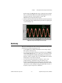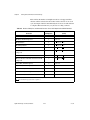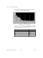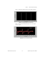
1
LabVIEW TM Digital Filter Design Toolkit User Manual Digital Filter Design Toolkit User Manual February 2005 371353A-01 Support Worldwide Technical Support and Product Information ni.com National Instruments Corporate Headquarters 11500 North Mopac Expressway Austin, Texas 78759-3504 USA Tel: 512 683 0100 Worldwide Offices Australia 1800 300 800, Austria 43 0 662 45 79 90 0, Belgium 32 0 2 757 00 20, Brazil 55 11 3262 3599, Canada (Calgary) 403 274 9391, Canada (Ottawa) 613 233 5949, Canada (Québec) 450 510 3055, Canada (Toronto) 905 785 0085, Canada (Vancouver) 604 685 7530, China 86 21 6555 7838, Czech Republic 420 224 235 774, Denmark 45 45 76 26 00, Finland 385 0 9 725 725 11, France 33 0 1 48 14 24 24, Germany 49 0 89 741 31 30, India 91 80 51190000, Israel 972 0 3 6393737, Italy 39 02 413091, Japan 81 3 5472 2970, Korea 82 02 3451 3400, Malaysia 603 9131 0918, Mexico 01 800 010 0793, Netherlands 31 0 348 433 466, New Zealand 0800 553 322, Norway 47 0 66 90 76 60, Poland 48 22 3390150, Portugal 351 210 311 210, Russia 7 095 783 68 51, Singapore 65 6226 5886, Slovenia 386 3 425 4200, South Africa 27 0 11 805 8197, Spain 34 91 640 0085, Sweden 46 0 8 587 895 00, Switzerland 41 56 200 51 51, Taiwan 886 2 2528 7227, Thailand 662 992 7519, United Kingdom 44 0 1635 523545 For further support information, refer to the Technical Support and Professional Services appendix. To comment on National Instruments documentation, refer to the National Instruments Web site at ni.com/info and enter the info code feedback. © 2005 National Instruments Corporation. All rights reserved. Important Information Warranty The media on which you receive National Instruments software are warranted not to fail to execute programming instructions, due to defects in materials and workmanship, for a period of 90 days from date of shipment, as evidenced by receipts or other documentation. National Instruments will, at its option, repair or replace software media that do not execute programming instructions if National Instruments receives notice of such defects during the warranty period. National Instruments does not warrant that the operation of the software shall be uninterrupted or error free. A Return Material Authorization (RMA) number must be obtained from the factory and clearly marked on the outside of the package before any equipment will be accepted for warranty work. National Instruments will pay the shipping costs of returning to the owner parts which are covered by warranty. National Instruments believes that the information in this document is accurate. The document has been carefully reviewed for technical accuracy. In the event that technical or typographical errors exist, National Instruments reserves the right to make changes to subsequent editions of this document without prior notice to holders of this edition. The reader should consult National Instruments if errors are suspected. In no event shall National Instruments be liable for any damages arising out of or related to this document or the information contained in it. EXCEPT AS SPECIFIED HEREIN, NATIONAL INSTRUMENTS MAKES NO WARRANTIES, EXPRESS OR IMPLIED, AND SPECIFICALLY DISCLAIMS ANY WARRANTY OF MERCHANTABILITY OR FITNESS FOR A PARTICULAR PURPOSE. CUSTOMER’S RIGHT TO RECOVER DAMAGES CAUSED BY FAULT OR NEGLIGENCE ON THE PART OF NATIONAL INSTRUMENTS SHALL BE LIMITED TO THE AMOUNT THERETOFORE PAID BY THE CUSTOMER. NATIONAL INSTRUMENTS WILL NOT BE LIABLE FOR DAMAGES RESULTING FROM LOSS OF DATA, PROFITS, USE OF PRODUCTS, OR INCIDENTAL OR CONSEQUENTIAL DAMAGES, EVEN IF ADVISED OF THE POSSIBILITY THEREOF. This limitation of the liability of National Instruments will apply regardless of the form of action, whether in contract or tort, including negligence. Any action against National Instruments must be brought within one year after the cause of action accrues. National Instruments shall not be liable for any delay in performance due to causes beyond its reasonable control. The warranty provided herein does not cover damages, defects, malfunctions, or service failures caused by owner’s failure to follow the National Instruments installation, operation, or maintenance instructions; owner’s modification of the product; owner’s abuse, misuse, or negligent acts; and power failure or surges, fire, flood, accident, actions of third parties, or other events outside reasonable control. Copyright Under the copyright laws, this publication may not be reproduced or transmitted in any form, electronic or mechanical, including photocopying, recording, storing in an information retrieval system, or translating, in whole or in part, without the prior written consent of National Instruments Corporation. Trademarks National Instruments, NI, ni.com, and LabVIEW are trademarks of National Instruments Corporation. Refer to the Terms of Use section on ni.com/legal for more information about National Instruments trademarks. Other product and company names mentioned herein are trademarks or trade names of their respective companies. Members of the National Instruments Alliance Partner Program are business entities independent from National Instruments and have no agency, partnership, or joint-venture relationship with National Instruments. Patents For patents covering National Instruments products, refer to the appropriate location: Help»Patents in your software, the patents.txt file on your CD, or ni.com/patents. WARNING REGARDING USE OF NATIONAL INSTRUMENTS PRODUCTS (1) NATIONAL INSTRUMENTS PRODUCTS ARE NOT DESIGNED WITH COMPONENTS AND TESTING FOR A LEVEL OF RELIABILITY SUITABLE FOR USE IN OR IN CONNECTION WITH SURGICAL IMPLANTS OR AS CRITICAL COMPONENTS IN ANY LIFE SUPPORT SYSTEMS WHOSE FAILURE TO PERFORM CAN REASONABLY BE EXPECTED TO CAUSE SIGNIFICANT INJURY TO A HUMAN. (2) IN ANY APPLICATION, INCLUDING THE ABOVE, RELIABILITY OF OPERATION OF THE SOFTWARE PRODUCTS CAN BE IMPAIRED BY ADVERSE FACTORS, INCLUDING BUT NOT LIMITED TO FLUCTUATIONS IN ELECTRICAL POWER SUPPLY, COMPUTER HARDWARE MALFUNCTIONS, COMPUTER OPERATING SYSTEM SOFTWARE FITNESS, FITNESS OF COMPILERS AND DEVELOPMENT SOFTWARE USED TO DEVELOP AN APPLICATION, INSTALLATION ERRORS, SOFTWARE AND HARDWARE COMPATIBILITY PROBLEMS, MALFUNCTIONS OR FAILURES OF ELECTRONIC MONITORING OR CONTROL DEVICES, TRANSIENT FAILURES OF ELECTRONIC SYSTEMS (HARDWARE AND/OR SOFTWARE), UNANTICIPATED USES OR MISUSES, OR ERRORS ON THE PART OF THE USER OR APPLICATIONS DESIGNER (ADVERSE FACTORS SUCH AS THESE ARE HEREAFTER COLLECTIVELY TERMED “SYSTEM FAILURES”). ANY APPLICATION WHERE A SYSTEM FAILURE WOULD CREATE A RISK OF HARM TO PROPERTY OR PERSONS (INCLUDING THE RISK OF BODILY INJURY AND DEATH) SHOULD NOT BE RELIANT SOLELY UPON ONE FORM OF ELECTRONIC SYSTEM DUE TO THE RISK OF SYSTEM FAILURE. TO AVOID DAMAGE, INJURY, OR DEATH, THE USER OR APPLICATION DESIGNER MUST TAKE REASONABLY PRUDENT STEPS TO PROTECT AGAINST SYSTEM FAILURES, INCLUDING BUT NOT LIMITED TO BACK-UP OR SHUT DOWN MECHANISMS. BECAUSE EACH END-USER SYSTEM IS CUSTOMIZED AND DIFFERS FROM NATIONAL INSTRUMENTS' TESTING PLATFORMS AND BECAUSE A USER OR APPLICATION DESIGNER MAY USE NATIONAL INSTRUMENTS PRODUCTS IN COMBINATION WITH OTHER PRODUCTS IN A MANNER NOT EVALUATED OR CONTEMPLATED BY NATIONAL INSTRUMENTS, THE USER OR APPLICATION DESIGNER IS ULTIMATELY RESPONSIBLE FOR VERIFYING AND VALIDATING THE SUITABILITY OF NATIONAL INSTRUMENTS PRODUCTS WHENEVER NATIONAL INSTRUMENTS PRODUCTS ARE INCORPORATED IN A SYSTEM OR APPLICATION, INCLUDING, WITHOUT LIMITATION, THE APPROPRIATE DESIGN, PROCESS AND SAFETY LEVEL OF SUCH SYSTEM OR APPLICATION. Contents About This Manual Conventions ...................................................................................................................xii Related Documentation..................................................................................................xiii Chapter 1 Introduction to the LabVIEW Digital Filter Design Toolkit Digital Filter Design Process Overview ........................................................................1-1 LabVIEW Digital Filter Design Toolkit Overview .......................................................1-2 Generalized Remez and Least Pth Norm Design Algorithms .........................1-2 Large Selection of Filter Structures.................................................................1-2 Special Digital Filter Design ...........................................................................1-3 Fixed-Point Filter Design ................................................................................1-3 Code Generation for FPGA and DSP Targets.................................................1-3 Multirate Digital Filter Design ........................................................................1-3 Comprehensive Analysis Tools.......................................................................1-4 Note to Current LabVIEW Advanced Analysis Library Users .....................................1-4 Chapter 2 Digital Filter Design Basics Digital Filter Applications .............................................................................................2-1 Digital Filter Terminology.............................................................................................2-2 Filter Attributes ...............................................................................................2-2 FIR and IIR Filters...........................................................................................2-2 Mathematical Definitions..................................................................2-3 FIR Filters Versus IIR Filters............................................................2-4 Digital Filter Specifications ...........................................................................................2-5 Filter Type .......................................................................................................2-5 Sampling Frequency........................................................................................2-5 Filter Specifications.........................................................................................2-5 Design Methods...............................................................................................2-8 Digital Filter Analysis....................................................................................................2-9 Poles and Zeroes..............................................................................................2-9 Pole-Zero Plots ................................................................................................2-10 Summary ........................................................................................................................2-11 © National Instruments Corporation v Digital Filter Design Toolkit User Manual Contents Chapter 3 Getting Started with Floating-Point Filter Design Typical Floating-Point Digital Filter Design Process ................................................... 3-1 Designing Floating-Point Filters ................................................................................... 3-1 Entering Filter Specifications.......................................................................... 3-2 Entering Filter Specifications in the Text-Based Interface of Digital Numeric Controls .......................................................... 3-3 Entering Filter Specifications in the Graphical Interface ................. 3-3 Selecting the Design Method .......................................................................... 3-4 Analyzing the Filter Design ............................................................................ 3-6 Magnitude Response......................................................................... 3-6 Pole-Zero Plot................................................................................... 3-6 Filter Order Specification ................................................................. 3-6 Example: Designing a Lowpass Digital Filter According to Specifications................. 3-7 Example: Filtering ......................................................................................................... 3-8 Summary........................................................................................................................ 3-9 Chapter 4 Getting Started with Fixed-Point Filter Design Typical Fixed-Point Digital Filter Design Process........................................................ 4-1 Implementing Fixed-Point Filters.................................................................................. 4-3 Selecting a Filter Structure.............................................................................. 4-3 Selecting Structures for FIR Filters .................................................. 4-4 Selecting Structures for IIR Filters ................................................... 4-4 Using Lattice Structures ................................................................... 4-5 Modeling Fixed-Point Filters .......................................................................... 4-8 Modeling Quantizers ........................................................................ 4-9 Setting wl and iwl............................................................... 4-10 Setting Overflow Mode...................................................... 4-10 Setting Round-Off Mode.................................................... 4-11 Setting Quantizers Manually ............................................................ 4-11 Validating Fixed-Point Filters......................................................................... 4-11 Fixed-Point Filter Analysis............................................................... 4-11 Example: Analyzing a Fixed-Point Filter ......................................... 4-12 Fixed-Point Filter Simulation ........................................................... 4-14 Example: Simulating a Fixed-Point Filter ........................................ 4-15 Generating Code ............................................................................................. 4-17 Extracting Fixed-Point Integer Coefficients..................................... 4-17 Generating Fixed-Point C Code ....................................................... 4-18 Generating Fixed-Point LabVIEW Code ......................................... 4-19 Integer LabVIEW Code ..................................................... 4-21 SCTL-Optimized LabVIEW FPGA Code.......................... 4-23 Digital Filter Design Toolkit User Manual vi ni.com Contents Example: Generating LabVIEW Code for FPGA Devices from a Fixed-Point Filter Model................................................................4-25 Summary ........................................................................................................................4-27 Chapter 5 Advanced and Special Filter Design Linear Phase and Minimum Phase Filters .....................................................................5-1 Mathematical Definition..................................................................................5-1 Types of Linear Phase FIR Filters...................................................................5-2 Linear Phase FIR Filter Example ....................................................................5-4 Hilbert Transformers......................................................................................................5-5 Type IV Hilbert Transformers.........................................................................5-5 Type III Hilbert Transformers .........................................................................5-7 Differentiators ................................................................................................................5-8 Type IV Differentiator.....................................................................................5-8 Type III Differentiator.....................................................................................5-9 Notch/Peak Filters..........................................................................................................5-11 Notch Filter Example ......................................................................................5-11 Comb Filters ..................................................................................................................5-14 Comb Filter Example ......................................................................................5-15 Arbitrary Shaped Filters.................................................................................................5-18 Linear Phase FIR Filter with Arbitrary Magnitude Response.........................5-18 Arbitrary Magnitude Filter Example.................................................5-18 Inverse Sinc Compensation Filter Example......................................5-19 IIR Filter with Arbitrary Magnitude Response ...............................................5-20 Group Delay Compensator ............................................................................................5-21 Group Delay Compensator Example...............................................................5-22 Narrowband FIR Filters .................................................................................................5-23 Narrowband Filter Example ............................................................................5-25 Summary ........................................................................................................................5-26 Chapter 6 Multirate Digital Filters Multirate Digital Filter Basics .......................................................................................6-1 Resampling ......................................................................................................6-2 Decimation ......................................................................................................6-2 Decimation Filter Example ...............................................................6-4 Interpolation ....................................................................................................6-4 Interpolation Filter Example .............................................................6-6 Multistage Multirate Filters.............................................................................6-7 Multistage Decimation Filter Example .............................................6-7 © National Instruments Corporation vii Digital Filter Design Toolkit User Manual Contents Cascaded Integrator Comb (CIC) Filters ........................................................ 6-9 Zero Phase Filtering ........................................................................................ 6-10 Multirate Filter Design .................................................................................................. 6-11 Single-Stage Multirate Filter Design .............................................................. 6-12 Multistage Multirate Filter Design.................................................................. 6-13 Nyquist Filter Design ...................................................................................... 6-14 Nyquist Filters .................................................................................. 6-15 Raised Cosine Filters ........................................................................ 6-16 Halfband Filters ................................................................................ 6-17 Multirate Filter Analysis................................................................................................ 6-17 Multirate Filter Signal Processing ................................................................................. 6-17 Summary........................................................................................................................ 6-18 Chapter 7 Advanced Techniques for Designing Filters Remez Design Method .................................................................................................. 7-1 Using the Remez Design VI............................................................................ 7-2 Specifying the Target Frequency Response ..................................... 7-2 Specifying the Filter Order ............................................................... 7-3 Selecting the Filter Type................................................................... 7-3 Symmetric and Antisymmetric Filter Types ...................... 7-4 Differentiator and Hilbert Filter Types .............................. 7-4 Minimum and Maximum Phase Filter Types..................... 7-4 FIR Magnitude Approximation....................................................................... 7-4 Minimum and Maximum Phase FIR Design .................................... 7-5 Designing Minimum and Maximum Phase Filters with the DFD Remez Design VI.................................................... 7-7 Single-Point Bands.......................................................................................... 7-8 Exact Gain Control.......................................................................................... 7-9 Ripple Constraint ............................................................................................ 7-12 Least Pth Norm Design Method .................................................................................... 7-14 Using the DFD Least Pth Norm Design VI .................................................... 7-16 Specifying the Target Frequency Response ..................................... 7-16 Specifying the Filter Order ............................................................... 7-16 Specifying Order of Norm ................................................................ 7-17 Specifying Pole Radius Constraint ................................................... 7-17 Least Pth Norm Linear Phase FIR Design ...................................................... 7-17 Approximated Linear Phase IIR Design ......................................................... 7-19 Minimum and Maximum Phase IIR Design ................................................... 7-21 Summary........................................................................................................................ 7-22 Digital Filter Design Toolkit User Manual viii ni.com Contents Appendix A References Appendix B Technical Support and Professional Services © National Instruments Corporation ix Digital Filter Design Toolkit User Manual About This Manual The LabVIEW Digital Filter Design Toolkit provides a collection of advanced digital filter design tools to supplement the LabVIEW Full Development System. With the Digital Filter Design Toolkit, you can design, analyze, and simulate floating-point and fixed-point digital filters. This manual contains information you need to understand the digital filter design process and how to use the Digital Filter Design (DFD) Toolkit VIs to design floating-point and fixed-point digital filters. Use the following questions and answers to assess how you should get started with the Digital Filter Design Toolkit. Are you new to LabVIEW and need more information about getting results with LabVIEW? Refer to the Getting Started with LabVIEW manual for information about using LabVIEW. You can access all LabVIEW development system documentation through the LabVIEW Bookshelf, available by selecting Start»All Programs»National Instruments»LabVIEW 7.1»Search the LabVIEW Bookshelf. Are you new to digital filter design and need more information about the basics? Read Chapter 2, Digital Filter Design Basics, for general information about digital filters. Do you want help designing a classical floating-point or fixed-point digital filter? Read Chapter 3, Getting Started with Floating-Point Filter Design, and Chapter 4, Getting Started with Fixed-Point Filter Design. These chapters are designed to help users with little to no filtering experience design classical floating-point and fixed-point digital filters. You can follow the examples in these chapters to learn more about each step of the design process. Each example builds on the previous example—from entering filter specifications to generating LabVIEW code for a hardware target. You can find the examples in the examples\Digital Filter Design\CaseStudy1 directory. © National Instruments Corporation xi Digital Filter Design Toolkit User Manual About This Manual Do you understand digital filter design basics but need to experiment with examples, or are you looking for a starting point? The examples provided with this toolkit offer a starting point for many common digital filter design problems. Use the NI Example Finder by selecting Help»Find Examples in LabVIEW to search for examples that best match the design problem. You can use those examples as a starting point. Do you need to design advanced or special filters? Read Chapters 5–7 for information about designing advanced and special filters, including notch/peak filters, comb filters, narrowband filters, group delay compensators, and multirate filters. These chapters assume that you already know about filtering. Are you interested in learning the mathematics behind digital filter design? This manual focuses on explaining how you can use the Digital Filter Design Toolkit to design a digital filter that meets a set of specifications. If you want to learn digital filter design theory, refer to Appendix A, References, for a list of resources that explain the theory and algorithms implemented in the Digital Filter Design Toolkit. Conventions The following conventions appear in this manual: » The » symbol leads you through nested menu items and dialog box options to a final action. The sequence File»Page Setup»Options directs you to pull down the File menu, select the Page Setup item, and select Options from the last dialog box. This icon denotes a tip, which alerts you to advisory information. This icon denotes a note, which alerts you to important information. bold Bold text denotes items that you must select or click in the software, such as menu items and dialog box options. Bold text also denotes parameter names. italic Italic text denotes variables, emphasis, a cross reference, or an introduction to a key concept. This font also denotes text that is a placeholder for a word or value that you must supply. Digital Filter Design Toolkit User Manual xii ni.com About This Manual monospace Text in this font denotes text or characters that you should enter from the keyboard, sections of code, programming examples, and syntax examples. This font is also used for the proper names of disk drives, paths, directories, programs, subprograms, subroutines, device names, functions, operations, variables, filenames, and extensions. monospace italic Italic text in this font denotes text that is a placeholder for a word or value that you must supply. Related Documentation The following documents contain information that you might find helpful as you read this manual: • Getting Started with LabVIEW, available as a printed manual in your LabVIEW development system box or by selecting Start»All Programs»National Instruments»LabVIEW 7.1»Search the LabVIEW Bookshelf • LabVIEW Help, available by selecting Help»VI, Function, & How-To Help © National Instruments Corporation xiii Digital Filter Design Toolkit User Manual 1 Introduction to the LabVIEW Digital Filter Design Toolkit The LabVIEW Digital Filter Design Toolkit includes several advanced filter design tools for designing, analyzing, and simulating floating-point and fixed-point digital filters. This chapter discusses the general digital filter design process and introduces the tools in the Digital Filter Design Toolkit that you can use to design digital filters. Note If you currently use VIs from the Analyze palette in the LabVIEW Full or Professional Development System for filter design, refer to the Note to Current LabVIEW Advanced Analysis Library Users section in this chapter for information about transitioning from those VIs or using those VIs with the Digital Filter Design Toolkit VIs. Digital Filter Design Process Overview Digital filter design involves the following three steps: 1. Specifying the design method and target digital filter attributes, or the characteristics you want the digital filter to possess. Refer to Chapter 2, Digital Filter Design Basics, for general information about digital filter specifications. Refer to Chapter 3, Getting Started with Floating-Point Filter Design, to learn how to use the Digital Filter Design Toolkit to enter digital filter specifications. 2. Analyzing the characteristics of the floating-point digital filter you designed in Step 1. Refer to Chapter 2, Digital Filter Design Basics, for information about evaluating the characteristics of a digital filter. 3. For fixed-point targets, implementing the filter with finite-precision arithmetic. Refer to Chapter 4, Getting Started with Fixed-Point Filter Design, to learn about implementing fixed-point digital filters with the Digital Filter Design Toolkit. The design process is iterative. You often might experiment with different design specifications or design methods to develop the appropriate digital filter for an application. Sometimes you might need to revise the specifications or modify the design method after you test the filter, © National Instruments Corporation 1-1 Digital Filter Design Toolkit User Manual Chapter 1 Introduction to the LabVIEW Digital Filter Design Toolkit especially when developing fixed-point filters because of finite-precision effects. LabVIEW Digital Filter Design Toolkit Overview The Digital Filter Design Toolkit includes a variety of tools to help you design digital filters without requiring you to have advanced knowledge of digital signal processing or digital filtering techniques. For example, the Digital Filter Design Toolkit includes Express VIs, which you can use to interact graphically with filter specifications to design appropriate digital filters. In addition to tools that help you create digital filters quickly, the Digital Filter Design Toolkit includes tools for conventional and multirate digital filter design, floating-point to fixed-point conversion, filter analysis, and simulation on a desktop computer, as described in the following sections. For complete reference information, refer to the LabVIEW Help by selecting Help»VI, Function, & How-To Help in LabVIEW. Generalized Remez and Least Pth Norm Design Algorithms You can use algorithms such as the generalized Remez method and the least pth norm method to specify arbitrary magnitude and phase response for a digital filter. The toolkit includes automatic order-estimation VIs to assist you with estimating the filter order. Refer to Chapter 7, Advanced Techniques for Designing Filters, for information about using the DFD Remez Design VI and the DFD Least Pth Norm Design VI. Large Selection of Filter Structures When you design digital filters with the Digital Filter Design Toolkit, you can select from one of 23 possible digital filter structures, which range from the direct form and cascaded form to Lattice AR (Auto-Regressive), Lattice MA (Moving Average), and Lattice ARMA (Auto-Regressive and Moving Average). Filter structures are mathematically equivalent when you use floating-point computation. However, different structures can have markedly different performance in fixed-point implementations and can lead to different computation complexity and memory usage in fixed-point or floating-point implementations. Selecting an appropriate filter structure is critical for digital filter design, especially for fixed-point digital filters in which the Digital Filter Design Toolkit User Manual 1-2 ni.com Chapter 1 Introduction to the LabVIEW Digital Filter Design Toolkit precision of the filter coefficients and filtering operations is more limited than for floating-point digital filters. Refer to Chapter 4, Getting Started with Fixed-Point Filter Design, for information about applying different filter structures. Special Digital Filter Design The Special Filter Design VIs help you design IIR notch/peak filters, IIR comb filters, maximally flat filters, narrowband filters, and group delay compensators. Refer to Chapter 5, Advanced and Special Filter Design, for information about using the Special Filter Design VIs. Fixed-Point Filter Design The Fixed-Point Tools VIs help you quantize filter coefficients, model and simulate the fixed-point filter design, and analyze the fixed-point filter design. You can save the resulting fixed-point filter information in C code for implementation on DSP chips or in LabVIEW code for implementation on NI FPGA devices using the DFD FXP Code Generator VI. The Fixed-Point Tools VIs make the Digital Filter Design Toolkit an important part of NI embedded system development. Refer to Chapter 4, Getting Started with Fixed-Point Filter Design, for information about developing fixed-point filters with the Fixed-Point Tools VIs. Code Generation for FPGA and DSP Targets You can use the DFD FXP Code Generator VI to automatically generate C and LabVIEW code that you can deploy to DSPs and NI FPGA devices. You can generate LabVIEW code specifically optimized for NI FPGA devices using the SCTL-Optimized LabVIEW FPGA code option. Refer to Chapter 4, Getting Started with Fixed-Point Filter Design, for information about generating code using the DFD FXP Code Generator VI. Multirate Digital Filter Design The Multirate Filter Design VIs help you design, analyze, and implement single-stage multirate filters, multistage multirate filters, halfband filters, Nyquist filters, raised cosine filters, and cascaded integrator comb (CIC) filters. Refer to Chapter 6, Multirate Digital Filters, for information about using the Multirate Filter Design VIs. © National Instruments Corporation 1-3 Digital Filter Design Toolkit User Manual Chapter 1 Introduction to the LabVIEW Digital Filter Design Toolkit Comprehensive Analysis Tools You can use the Filter Analysis VIs to evaluate the characteristics of filters you design with the Filter Design VIs. You can examine frequency response, group delay, phase delay, impulse response, step response, and pole-zero placement. Refer to Chapter 2, Digital Filter Design Basics, for general information about evaluating digital filters you create with the Digital Filter Design Toolkit. Note to Current LabVIEW Advanced Analysis Library Users The LabVIEW Advanced Analysis Library, which is accessible through the Analyze palette, is a collection of VIs that perform waveform measurements, waveform conditioning, waveform monitoring, waveform generation, signal processing, point-by-point analysis, and mathematical calculations. The Advanced Analysis Library contains some digital filter design VIs similar to VIs in the Digital Filter Design Toolkit. For example, the Butterworth Coefficients VI in the Advanced Analysis Library is similar to the DFD Butterworth Design VI and the Parks-McClellan VI in the Advanced Analysis Library is similar to the DFD Remez Design VI. However, the Digital Filter Design Toolkit VIs provide greater capabilities, including, but not limited to, support for arbitrary phase and magnitude specifications and fixed-point filter design. Although the VIs have similar functionality, the results you achieve might not be exactly the same because the design algorithms are different. Refer to the NI Web site at ni.com/info and enter the info code dfdinfo for information about using the LabVIEW Analyze VIs with the Digital Filter Design Toolkit VIs. Digital Filter Design Toolkit User Manual 1-4 ni.com Digital Filter Design Basics 2 This chapter contains introductory information about digital filter design for users who might not have had formal DSP or digital filter design training. You can apply digital filters without knowing or understanding much of the mathematics behind the filters. This chapter discusses general digital filter applications, standard terminology, design principles, and analysis techniques you need to design and analyze the characteristics of a digital filter. Digital Filter Applications Filters are signal processing elements that alter the frequency spectrum of an input signal. You might use filters for the following applications: • Attenuating noise in a signal where the noise power and signal power are concentrated at different frequencies. For example, you might use a notch filter to attenuate a 60 Hz powerline interference present in a signal. • Extracting signal components from a signal that contains different signal components concentrated at different frequencies. For example, you might use a bandpass filter to extract a particular radio station signal from a received broadband radio signal. • Reshaping the frequency spectrum of the input signal. For example, you might use an A-weighting filter to approximate the frequency response of a human ear. As another example, you might use an equalizer filter to undo magnitude and phase distortion caused by passing a signal through a linear time-invariant communications channel. You can use either fixed-point or floating-point arithmetic to implement digital signal processing systems. Although floating-point implementations are typically easier to design, fixed-point implementations are often less expensive and more power efficient than floating-point implementations. Floating-point designs are typically appropriate in applications that run on desktop computers, and fixed-point designs are often more appropriate in embedded applications, in which it can be important to minimize cost or power consumption. © National Instruments Corporation 2-1 Digital Filter Design Toolkit User Manual Chapter 2 Digital Filter Design Basics Digital Filter Terminology When you design a digital filter, you begin by creating specifications that define the characteristics you want in the digital filter. This section explains the characteristics of digital filters you create using the Digital Filter Design Toolkit. Filter Attributes The filters you design using the Digital Filter Design Toolkit are the following: • Linear—The output signals of digital filters are linear functions of the input signals. You cannot use these digital filters to equalize non-linear distortion caused by passing a signal through a non-linear peak-clipping or truncating channel. • Time invariant—The frequency response of the digital filter is fixed versus time. Alternatively, adaptive filters, which are outside the scope of the Digital Filter Design Toolkit, can adapt their frequency response versus time in response to a time-variant target response. • Causal—The output signal of the digital filter cannot change in response to a change in an input signal until after the input signal changes. The Digital Filter Design Toolkit specifically creates digital filters that you treat as causal in applications, but you can use them in some non-causal applications. For example, a common DSP technique for linearizing the phase of a filter with non-linear phase is to pass the input signal through the filter, time-reverse the input signal, and then pass it through the filter again. In this case, the filter is acting non-causally. • Digital—The expected filter input signal is a series of discrete digital values. The set of discrete digital coefficients determines the filter frequency response. Digital filters have many advantages over analog filters. For example, the frequency response of digital filters generally does not depend on the parametric variation of electronic components or power supply noise or droop. FIR and IIR Filters You can design both FIR and IIR digital filters using the Digital Filter Design Toolkit: • Digital Filter Design Toolkit User Manual FIR (Finite Impulse Response)—After an input signal is set to zero, the filter output signal can be non-zero for only a finite number of sample times before it also becomes zero. 2-2 ni.com Chapter 2 • Digital Filter Design Basics IIR (Infinite Impulse Response)—The output signal from the filter can be non-zero infinitely after the input signal is changed from non-zero to zero. The choice between FIR and IIR filters affects both the filter design process and the implementation of the filter, as explained in the following sections. Mathematical Definitions In the time domain, the filtering process for FIR filters is defined mathematically as a convolution of N+1 filter coefficients bk with a sequence of input data samples x[n]: N y[n] = ∑ b x[n – k] k (2-1) k=0 where y[n] is the output of the filter, and N is the filter order. The number of coefficients for the FIR filter is defined as the number of taps, which is N+1. If a single non-zero value is present at the input of the filter but all subsequent input samples are zero, the output of the filter in Equation 2-1 becomes zero after the filter processes N+1 input data samples. Because the duration of the non-zero response in this case is necessarily finite for finite N+1, the filter in Equation 2-1 is an FIR filter. In 1962, Charles Rader and Bernard Gold at MIT Lincoln Laboratory, motivated by a digital vocoder (voice coder) application, devised the idea of using recursive digital filters. This innovation led to the IIR filter, which has a time-domain response defined by the following equation: N M ∑ a y[n – i] = ∑ b x[n – k] i k (2-2) k=0 i=0 where N is the numerator order and M is the denominator order. The filter in Equation 2-2 operates on current input x[n] and previous input x[n–k] and current output y[n] and previous output y[n–i]. The impulse response of the filter in this case is infinite because the filter might generate non-zero outputs arbitrarily far into the future in response to a single non-zero input sample. © National Instruments Corporation 2-3 Digital Filter Design Toolkit User Manual Chapter 2 Digital Filter Design Basics For most filtering applications, FIR filters are sufficient. In general, FIR filters make better use of available precision and they are more numerically robust. However, in some cases FIR filters become impractically large. For example, if you need a large number of FIR filter coefficients—perhaps hundreds or more—an FIR filter might be too difficult or expensive to implement because the design might require more memory, more power, more processing time, and more engineering time to optimize the design. FIR Filters Versus IIR Filters One difference between FIR and IIR filters is the impulse response, which is finite or infinite, respectively. That difference alone is not likely to be important as you design a filter, but FIR and IIR filters have other differences that might affect the design. For example, FIR filter implementations typically require more multiplications and summations than IIR filters with similar filtering performance. However, because computer architectures are frequently better suited to performing FIR filtering, the computation speed of an IIR filter is not necessarily faster than an FIR filter. Table 2-1 compares the attributes of causal FIR and IIR digital filters. Table 2-1. FIR Filter Attributes versus IIR Filter Attributes Attribute FIR Filter IIR Filter Exactly linear phase response possible Possible Not possible Stability Always stable Conditionally stable Fixed-point version Easy to implement Can be complicated to implement Computational complexity More computations Fewer computations Datapath precision typically required Less precision required Greater precision required Zero-input limit cycles1 Cannot produce limit cycles Might produce limit cycles 1 “Zero-input limit cycle behavior refers to the effect that the output may continue to oscillate indefinitely with a periodic pattern while the input remains equal to zero. And it is a consequence either of the nonlinear quantizers in the feedback loop of IIR filter or of overflow of additions.” (Oppenheim and Schafer) Digital Filter Design Toolkit User Manual 2-4 ni.com Chapter 2 Digital Filter Design Basics Digital Filter Specifications To design a digital filter with the Digital Filter Design Toolkit, you must specify the filter type, sampling frequency, filter specifications, and design method. Filter Type You can create lowpass, highpass, bandpass, and bandstop filters. • A lowpass filter allows low frequencies to pass and attenuates high frequencies. • A highpass filter allows high frequencies to pass and attenuates low frequencies. • A bandpass filter allows a range of frequencies to pass. • A bandstop filter attenuates a range of frequencies and allows all frequencies not within the range to pass. Sampling Frequency The symbol fs denotes the sampling frequency, which is the expected rate at which the input signal for the filter is sampled. One-half of the sampling frequency is called the Nyquist frequency. In this toolkit, the default sampling frequency is 1, which is the normalized sampling frequency. Filter Specifications For most digital filters, you typically design the digital filter response in the frequency domain. The frequency response specification for the digital filter typically includes the target magnitude response, phase response, and the allowable deviation for each. Figure 2-1 illustrates a lowpass filter specification. © National Instruments Corporation 2-5 Digital Filter Design Toolkit User Manual Chapter 2 Digital Filter Design Basics Magnitude Response δp stopband attenuation transition band δs 0 passband edge frequency stopband edge frequency fs /2 Frequency Figure 2-1. Lowpass Filter Specifications You must define the following parameters in a filter specification: passband gain, maximum passband ripple, passband edge frequencies, stopband edge frequencies, and minimum stopband attenuation (alternatively, maximum stopband gain). The passband ripple defines the maximum allowable deviation δp from the desired passband gain. Minimum stopband attenuation indicates the maximum allowable deviation δs from zero stopband gain. Notice the transition band between the passband and stopband frequencies. In an ideal design, a digital filter has the target gain in the passband and zero gain (–∞ dB) in the stopband. In a real implementation, a finite transition region between the passband and the stopband, which is known as the transition band, always exists. The gain of the filter in the transition band is unspecified. The gain usually changes gradually through the transition band from 1 (0 dB) in the passband to 0 (–∞ dB) in the stopband. Digital Filter Design Toolkit User Manual 2-6 ni.com Chapter 2 Digital Filter Design Basics Figure 2-2, Figure 2-3, and Figure 2-4 illustrate the magnitude frequency responses of highpass, bandpass, and bandstop filters. Magnitude Response δp passband gain transition band δs 0 stopband edge frequency fs /2 passband edge frequency Frequency Figure 2-2. Highpass Filter Specifications Magnitude Response δp transition band transition band δs δs 0 stopband edge frequency 1 passband edge frequency 1 Frequency passband edge frequency 2 stopband edge frequency 2 fs /2 Figure 2-3. Bandpass Filter Specifications © National Instruments Corporation 2-7 Digital Filter Design Toolkit User Manual Chapter 2 Digital Filter Design Basics δp Magnitude Response δp transition band transition band δs 0 passband edge frequency 1 stopband edge frequency 1 Frequency stopband edge frequency 2 passband edge frequency 2 fs /2 Figure 2-4. Bandstop Filter Specifications Design Methods The Digital Filter Design Toolkit provides several design methods, including Elliptic, Chebyshev, Inverse Chebyshev, and Butterworth, for IIR digital filters. Each design option offers different characteristics. For example, Butterworth filters characteristically have a smooth response at all frequencies and also are monotonically decreasing or increasing in the transition band. However, Butterworth filters do not always provide an acceptably accurate approximation of the ideal filter response because the filter has slow roll off in the transition band. If you need sharper roll off than a Butterworth filter can provide, use a Chebyshev, Inverse Chebyshev, or Elliptic design. Refer to the LabVIEW Help for complete reference information on the Filter Design VIs and different design methods. The toolkit also provides several design methods, including the Kaiser Window method and the Remez algorithm, for FIR digital filters. The window-based methods are classical, while the Remez algorithm is complicated but provides optimal results. Use the DFD Classical Filter Design Express VI to experiment interactively with design methods. Refer to Chapter 3, Getting Started with Floating-Point Filter Design, for more information about design methods and using the DFD Classical Filter Design Express VIs. Digital Filter Design Toolkit User Manual 2-8 ni.com Chapter 2 Digital Filter Design Basics Digital Filter Analysis After you design a digital filter, you need to analyze the characteristics of the digital filter by evaluating the magnitude response, phase response and group delay, impulse response, or poles and zeroes. The Digital Filter Design Toolkit provides the Filter Analysis VIs to help you evaluate the characteristics of a filter. The following sections provide information about poles and zeroes and using the DFD Plot Pole-Zero VI. Refer to the LabVIEW Help for information about all Filter Analysis VIs. Poles and Zeroes The z-transform of an FIR filter is defined as N H(z) = ∑b N kz –k = K ∏ (1 – z kz –1 ) (2-3) k=1 k=0 j2πf where z ≡ e , bk are the filter coefficients, N denotes the order of the FIR filter, and K is the gain. In Equation 2-3, zk are the roots of polynomial H(z). H(zk) = 0 for all zk, so zk are called zeroes of the filter H(z). The number of zeroes in a filter must equal the filter order N. Similarly, the z-transform of the IIR filter in Equation 2-2 is defined as N ∑b z N ∏ (1 – z z –k –1 k k ) k=1 k=0 H ( z ) = ----------------------------- = K ----------------------------------M 1+ ∑a z i i=1 M –i ∏ (1 – p z k –1 (2-4) ) k=1 where zk and pk represent the roots of the numerator polynomial and denominator polynomial, respectively. pk are the poles of IIR filter H(z). IIR filters have poles and zeroes, and FIR filters have only zeroes. © National Instruments Corporation 2-9 Digital Filter Design Toolkit User Manual Chapter 2 Digital Filter Design Basics Pole-Zero Plots From a mathematical point of view, the pole-zero plot and frequency response provide the same information. Based on the frequency response, you can obtain a pole-zero plot. Conversely, from the pole-zero plot, you can compute the frequency response. Figure 2-5 illustrates a pole-zero plot for a particular IIR filter. The half-circle corresponds to |z| = 1, or the unit circle. The small circles along the half-circle represent zeroes. Each × represents a pole. Figure 2-5. Typical Pole-Zero Plot The pole-zero plot and frequency response characterize digital filters from the following perspectives: • You can determine whether a digital filter is stable; that is, whether the output of the digital filter is bounded for all possible bounded inputs. The necessary and sufficient condition for IIR filters to be stable is that all poles are inside the unit circle. In contrast, FIR filters are always stable because the FIR filters do not have poles. • You can determine if pole-zero pairs are close enough to effectively cancel out each other. Try deleting close pairs and checking the resulting frequency response. Fewer pole-zero pairs means fewer computations. Digital Filter Design Toolkit User Manual 2-10 ni.com Chapter 2 Digital Filter Design Basics Summary This section summarizes the main concepts presented in this chapter. • To design a digital filter, you first must enter the specifications for the filter you want to design. Specifications include the filter type, sampling frequency, passband ripple, passband and stopband frequencies, stopband attenuation, and design method. Refer to Chapter 3, Getting Started with Floating-Point Filter Design, for information about entering filter specifications when using the DFD Classical Filter Design Express VI. • You can create FIR and IIR filters using the Digital Filter Design Toolkit. In most cases, FIR filters make better use of precision and are more numerically robust. Refer to Table 2-1 for information about other FIR and IIR filter characteristics that might affect filter design. • You can create lowpass, highpass, bandpass, and bandstop digital filters using several different design methods. Refer to the LabVIEW Help for information about designing FIR and IIR filters using the Advanced FIR Filter Design VIs and the Advanced IIR Filter Design VIs. • After you design a digital filter, you must analyze the characteristics of the digital filter to make sure it meets the needs of the filtering application. Refer to the LabVIEW Help for information about the Filter Analysis VIs. © National Instruments Corporation 2-11 Digital Filter Design Toolkit User Manual 3 Getting Started with Floating-Point Filter Design This chapter explains how to use the interactive DFD Classical Filter Design Express VI to design classical floating-point digital filters. Typical Floating-Point Digital Filter Design Process Figure 3-1 illustrates the floating-point digital filter design process. You first design the specifications of the filter. You then analyze the characteristics of the resulting filter to determine if the filter meets the requirements of the system. If the filter does not meet the requirements of the system, you can modify the specifications and repeat the process. After you design an appropriate filter, you can use the filter in the system. Floating-Point Filter Design Floating-Point Analysis Floating-Point Filtering Figure 3-1. Floating-Point Digital Filter Design Process For a particular design problem, you can use several different techniques and filter types to yield an acceptable result. To achieve the best results, you might need to experiment with several different approaches. Designing Floating-Point Filters The main goal of digital filter design is to compute a set of coefficients so the characteristics of the resulting digital filter meet a set of predefined filter specifications. This section describes how you can use the DFD Classical Filter Design Express VI to design floating-point digital filters. © National Instruments Corporation 3-1 Digital Filter Design Toolkit User Manual Chapter 3 Getting Started with Floating-Point Filter Design Entering Filter Specifications You can use the DFD Classical Filter Design Express VI to interactively configure a classical digital filter. After you search the Functions palette for the Express VI and place it on the block diagram, the Configure Classical Filter Design dialog box appears, as shown in Figure 3-2. Figure 3-2. DFD Classical Filter Design Express VI Configuration Dialog Box From the configuration dialog box, you can select the filter type and design method from the pull-down menus and then enter the filter specifications through either the text-based interface of digital numeric controls on the left side of the configuration dialog box or the interactive graphical interface on the right side of the configuration dialog box. The results are equivalent. Refer to Chapter 2, Digital Filter Design Basics, for information about designing filter specifications, and then refer to the following sections for information about entering filter specifications into the configuration dialog box shown in Figure 3-2. Digital Filter Design Toolkit User Manual 3-2 ni.com Chapter 3 Getting Started with Floating-Point Filter Design Entering Filter Specifications in the Text-Based Interface of Digital Numeric Controls Classical digital filter specifications include frequency ranges and ripple constraints. You can specify the maximum allowable deviation δp from unity gain in the passband in the Passband Ripple numeric control. You can specify the maximum allowable deviation δs from the zero gain in the stopband in the Stopband Attenuation numeric control. You can specify deviations in either logarithmic or linear scale. The DFD Classical Filter Design Express VI uses logarithmic scale by default. To use a linear scale, remove the checkmark from the Magnitude in dB checkbox in the configuration dialog box. The following formulas show the relationship between logarithmic and linear scale: passband ripple (dB) = –20log10(1–δp) stopband attenuation (dB) = –20log10(δs) For example, if passband ripple = 0.01 dB (that is, 0.01 dB= –20log10(1 – δp)), δp= 0.00115. Similarly, if stopband attenuation = 60 dB (that is, 60 dB = –20log10(δs)), δs = 0.001. Entering Filter Specifications in the Graphical Interface The right side of Figure 3-2 displays the magnitude response of the designed digital filter. The magnitude axis can be either linear or logarithmic scale. Remove the checkmark from the Magnitude in dB checkbox to use a linear scale, or keep the checkmark in the Magnitude in dB checkbox to maintain a logarithmic scale. The Frequency axis, in hertz, covers the range from 0 to half the sampling frequency, which is the Nyquist frequency. The Magnitude graph contains a set of cursors that you can use to specify the passband and stopband. Use the passband cursor to change the passbands. The distance between unity and the horizontal passband cursor specifies the maximum passband ripple. The location of the vertical passband cursor indicates the passband edge frequency. The stopband cursors work in the same way to define the specifications of the stopbands. © National Instruments Corporation 3-3 Digital Filter Design Toolkit User Manual Chapter 3 Getting Started with Floating-Point Filter Design As you work with the cursors to define a filter specification, you must adhere to a set of rules to maintain valid specifications. If any rule is violated, the DFD Classical Filter Design Express VI displays a message in the Error Message indicator of the Configure Classical Filter Design dialog box with suggestions for repositioning the cursors. The rules are as follows: • Keep horizontal cursors in the range of (0, 1) in linear scale or (–inf, 0 dB) in logarithmic scale. • Keep the horizontal passband cursor above the horizontal stopband cursor. • Do not exchange the positions of vertical cursors. Selecting the Design Method After you enter the target digital filter specifications into the numeric controls or graphical interface, select a design method. The DFD Classical Filter Design Express VI provides the following FIR-based design methods: • Kaiser Window • Dolph-Chebyshev Window • Equi-Ripple FIR The Kaiser Window method and the Dolph-Chebyshev Window method are easier to design than the Equi-Ripple FIR method, but the Equi-Ripple FIR method yields optimal filters and often produces the best results for most FIR filter design problems. In addition to the FIR-based methods, the DFD Classical Filter Design Express VI supports the following IIR-based design methods: • Butterworth • Chebyshev • Inverse Chebyshev • Elliptic Figure 3-3 illustrates the magnitude responses of a typical lowpass filter designed by the four IIR-based methods. In each response, the filter order is equal to 5 in both the numerator and denominator. Digital Filter Design Toolkit User Manual 3-4 ni.com Chapter 3 Getting Started with Floating-Point Filter Design Figure 3-3. Comparison of the Magnitude Responses of Classical IIR Filters Table 3-1 summarizes the main features of the four IIR-based design methods so you can determine the IIR filter design method to use. Table 3-1. Comparison of Classical IIR Filters Ripple in Passband? Ripple in Stopband? Transition Bandwidth for a Fixed Order Order for Given Filter Specifications Butterworth No No Widest Highest Chebyshev Yes No Narrower Lower Inverse Chebyshev No Yes Narrower Lower Elliptic Yes Yes Narrowest Lowest IIR Filter When you design a digital filter with the DFD Classical Filter Design Express VI, the shape of the frequency response is controlled by the selected design method and the given filter specifications. You cannot alter the phase response, even though the phase response for filters generated with the FIR methods in this VI are linear phase. If you want to specify the magnitude response and phase response, use the Advanced IIR Filter Design VIs, Advanced FIR Filter Design VIs, or the Special Filter Design VIs. Refer to Chapter 5, Advanced and Special Filter Design, for information about designing special filters. © National Instruments Corporation 3-5 Digital Filter Design Toolkit User Manual Chapter 3 Getting Started with Floating-Point Filter Design Analyzing the Filter Design After you enter the target specification for a digital filter, you can immediately analyze the characteristics of the resulting filter in the configuration dialog box by evaluating the magnitude response, pole-zero plot, and the filter order. Magnitude Response The frequency response is given by H(e j2πf ), and the magnitude response is given by |H(e j2πf )|. For discrete-time systems, H(e j2πf ) is periodic with period of fs. For real-valued digital filters, the magnitude response is symmetric with respect to 0, ±fs, ±2fs,…. Therefore, the magnitude response is calculated only for [0, fs/2], the frequencies between 0 and the Nyquist frequency. The magnitude response graph in the Configure Classical Filter Design dialog box includes a thick, green vertical line to indicate the location of fs/2. Pole-Zero Plot In the Configure Classical Filter Design dialog box, a × represents a pole and a circle represents a zero. The poles of a causal stable filter must be inside the unit circle. Refer to Chapter 2, Digital Filter Design Basics, for more information about poles and zeroes. Filter Order Specification The DFD Classical Filter Design Express VI automatically computes the minimal filter order required to fulfill the given filter specification and displays the order in the Filter Order indicator. Given the same specification, different algorithms design digital filters with different filter orders. You can estimate the computational complexity and cost to some extent based on the filter order. If you have strict requirements for the system, filter order can help you determine if the filter is acceptable. Digital Filter Design Toolkit User Manual 3-6 ni.com Chapter 3 Getting Started with Floating-Point Filter Design Example: Designing a Lowpass Digital Filter According to Specifications Complete the following steps to experiment with a floating-point lowpass filter designed with the DFD Classical Filter Design Express VI and the following specifications: Specification Value Filter Type Lowpass Design Method Equi-Ripple Sampling Frequency 10 kHz Passband Frequency 0 to 100 Hz Passband Ripple ±0.0025 Stopband Frequency 800 Hz to 5 kHz Stopband Attenuation 60 dB 1. Open the Lowpass_Step 1_Design Lowpass VI located in the examples\Digital Filter Design\CaseStudy1 directory. 2. Examine the block diagram, as shown in Figure 3-4. Figure 3-4. Lowpass_Step 1_Design Lowpass VI Block Diagram 3. Double-click the Equi-Ripple FIR Lowpass Filter Express VI. The Configure Classical Filter Design dialog box appears. Note This Express VI was created using the DFD Classical Filter Design Express VI. After you enter specifications in the configuration dialog box and click the OK button, the name of the Express VI on the block diagram changes to reflect the type of filter you designed. In this example, the name changed to Equi-Ripple FIR Lowpass Filter. © National Instruments Corporation 3-7 Digital Filter Design Toolkit User Manual Chapter 3 Getting Started with Floating-Point Filter Design 4. Verify that the specifications in the configuration dialog box match the specifications listed in the table above. Because 60 dB stopband attenuation is equivalent to 0.001 stopband gain on a linear scale, the Stopband Attenuation numeric control contains 0.001 and the checkmark is removed from the Magnitude in dB checkbox to use a linear scale. 5. Use the magnitude response and pole-zero plots to verify that the characteristics of the resulting filter satisfy the specifications. 6. Click the OK button to close the Configure Classical Filter Design dialog box. 7. Run the VI and examine the resulting magnitude response on the front panel. Example: Filtering Complete the following steps to use the lowpass filter in a filtering application. 1. Open the Lowpass_Step 2_Perform Lowpass Filtering VI located in the examples\Digital Filter Design\CaseStudy1 directory. 2. Examine the block diagram, as shown in Figure 3-5. Figure 3-5. Lowpass_Step 2_Perform Lowpass Filtering VI Block Diagram Digital Filter Design Toolkit User Manual 3-8 ni.com Chapter 3 Getting Started with Floating-Point Filter Design In this example, the DFD Filtering VI has as inputs the lowpass digital filter created with the DFD Classical Filter Design Express VI and a signal that represents a typical signal in a system. The DFD Filtering VI outputs the filtered signal. 3. Switch to the front panel and run the VI. Notice that the VI plots both the original input signal and the filtered signal on the front panel graph, as shown in Figure 3-6. Figure 3-6. Original Input Signal and Filtered Signal Summary This section summarizes the main concepts presented in this chapter about the DFD Classical Filter Design Express VI. • Use the DFD Classical Filter Design Express VI to design a digital filter quickly and interactively. • You can enter target filter specifications in the interactive Configure Classical Filter Design dialog box, which opens automatically when you place the DFD Classical Filter Design Express VI on the block diagram or when you double-click on an existing DFD Classical Filter Design Express VI on the block diagram. • You can use the text-based interface of numeric controls or the graphical interface of the Express VI to fine-tune the target specifications. Both interfaces provide the same result, and you can clearly see the relationship between user-defined specifications and the characteristics of the resulting floating-point digital filter in terms of frequency response and pole-zero distribution. © National Instruments Corporation 3-9 Digital Filter Design Toolkit User Manual Chapter 3 Getting Started with Floating-Point Filter Design • The DFD Classical Filter Design Express VI provides three FIR-based design methods and four IIR-based design methods. You can interactively experiment with these design methods in the Configure Classical Filter Design dialog box. • If you want to specify the magnitude response and phase response or design a special filter, use the Advanced IIR Filter Deign VIs, Advanced FIR Filter Design VIs, or the Special Filter Design VIs. Refer to Chapter 5, Advanced and Special Filter Design, for information about designing special filters. Digital Filter Design Toolkit User Manual 3-10 ni.com Getting Started with Fixed-Point Filter Design 4 This chapter explains how to implement a fixed-point digital filter from a floating-point reference filter using the DFD Fixed-Point Tools VIs. This chapter assumes that you have read Chapter 3, Getting Started with Floating-Point Filter Design, or that you are already familiar with creating floating-point digital filters using the Digital Filter Design Toolkit. Typical Fixed-Point Digital Filter Design Process Fixed-point signal processing platforms, such as fixed-point digital signal processors (DSPs) and field-programmable gate arrays (FPGAs), are typically more power efficient and less expensive than floating-point alternatives. However, fixed-point systems are generally harder to design. For example, you must deal with the effects of the coarser quantization typically present in fixed-point systems. To design a fixed-point digital filter, you first must design a floating-point filter—also called a reference filter—that meets the target specifications. You then must modify the floating-point filter to accommodate the finite-precision constraints of the target platform while still trying to meet the target specifications. Figure 4-1 illustrates the fixed-point filter design process. © National Instruments Corporation 4-1 Digital Filter Design Toolkit User Manual Chapter 4 Getting Started with Fixed-Point Filter Design Floating-Point Filter Design Floating-Point Analysis Floating-Point Filtering Structure Selection Fixed-Point Modeling Fixed-Point Analysis Simulation Fixed-Point Target (DSP or FPGA) Figure 4-1. Fixed-Point Digital Filter Design Process Notice that after you design and analyze the floating-point reference filter, you select a filter structure and model the fixed-point design. Converting a floating-point filter to fixed-point form can significantly alter the characteristics and performance of the filter. You must analyze the filter and simulate the filtering process with data that is similar to the data in the actual system. Fixed-point arithmetic can have the following detrimental effects on filter performance: • Degraded signal-to-noise ratio from reduced precision of input signal samples • Distorted frequency response from limited word length representation of filter coefficients Digital Filter Design Toolkit User Manual 4-2 ni.com Chapter 4 Getting Started with Fixed-Point Filter Design • Limit cycles in IIR filters due to finite-precision arithmetic • Overflows or clipping due to insufficient headroom in datapaths Finally, you can generate code for the fixed-point target. Implementing Fixed-Point Filters Complete the following steps to convert a reference floating-point filter to a fixed-point filter, as illustrated in Figure 4-1. 1. Selecting an implementation structure for the filter. Refer to the Selecting a Filter Structure section for information about selecting and converting filter structures. 2. Modeling the fixed-point filter. To convert a floating-point filter to fixed-point, you must quantize the floating-point filter coefficients, the input signal, the output signal, and the intermediate operands. Quantization is the process of approximating each floating-point value by a fixed-point value that can be used in a fixed-point mathematical computation. Refer to the Modeling Fixed-Point Filters section for information about quantization. 3. Validating the fixed-point filter model using fixed-point analysis and simulation. If the fixed-point filter does not meet the given specifications, you can modify quantization settings, change the implementation structure, or refine the filter specifications for the reference filter. Refer to the Validating Fixed-Point Filters section for information about validating fixed-point filters. 4. Generating code for the modeled fixed-point filter for the designated hardware target. Refer to the Generating Code section for information about extracting filter coefficients and automatically generating C or LabVIEW code. This chapter presents examples and exercises that demonstrate each step. Selecting a Filter Structure A filter structure specifies how a given set of filter coefficients is used arithmetically to process an input signal stream. For a specified digital filter, dozens of mathematically equivalent implementation structures are available. For a floating-point digital filter, the effect of different implementation structures on filter behavior is negligible in most cases. For a fixed-point digital filter, different implementation structures can result in different outputs. © National Instruments Corporation 4-3 Digital Filter Design Toolkit User Manual Chapter 4 Getting Started with Fixed-Point Filter Design You can create FIR filters with the following structures: • FIR Direct Form • FIR Direct Form Transposed • FIR Symmetric • FIR Antisymmetric • Lattice MA (minimum phase) • Lattice MA (maximum phase) You can create IIR filters with the following structures: • IIR Direct Form • IIR Cascaded Second Order Sections Form • Lattice Allpass • Lattice AR • Lattice ARMA When you select a filter structure, you must balance a number of factors, including the type of filter (FIR or IIR), implementation resources, computational complexity, and sensitivity to coefficient quantization. Selecting Structures for FIR Filters For FIR filters, the FIR Direct Form structure is the simplest and most straightforward structure from the filter transfer function perspective. The FIR Direct Form Transposed structure is the alternative direct form implementation for FIR filters. Both direct form structures have the same computational complexity. The FIR Direct Form structure requires less memory for saving internal states. The FIR Direct Form Transposed structure has better timing performance if the filter is implemented in parallel. Use the FIR Direct Form structure if you want to implement FIR serially using a loop structure. For linear phase FIR filters, use the FIR Symmetric or FIR Antisymmetric structures, which use the symmetry or antisymmetry of the filter coefficients to reduce computational complexity and memory usage. Selecting Structures for IIR Filters The IIR Direct Form structure is the simplest IIR structure from the filter transfer function perspective. The IIR Direct Form structure usually has a low number of operations in implementation. However, its sensitivity to finite word length effects limits its use in fixed-point implementation. Use Digital Filter Design Toolkit User Manual 4-4 ni.com Chapter 4 Getting Started with Fixed-Point Filter Design the IIR Cascaded Second Order Sections Form to alleviate finite word length effects. The IIR Cascaded Second Order Sections Form II structure has the same computational complexity as Form I, but Form I requires more memory for saving internal states. Form II is the most frequently used structure. The advantages and disadvantages of using Form I and Form II and their transposed counterparts are the same as the FIR Direct Form and FIR Direct Form Transposed structures. Using Lattice Structures Lattice structures are good alternatives for fixed-point filter implementation. Lattice structures can preserve the stability of fixed-point IIR filters as long as the Lattice reflection coefficients have moduli smaller than one, no matter how limited the arithmetic precision is. The Digital Filter Design Toolkit provides the following three categories of Lattice structures: • Basic Section Type—Two multipliers per Lattice section. This category offers the most general Lattice structure. • One Multiplier Section Type—Only one multiplier per Lattice section. This category saves certain resources for hardware targets like FPGAs. • Normalized Section Type—Four multipliers per Lattice section. This category automatically scales the internal signals to help minimize quantization effects in each lattice section at the cost of increasing the implementation complexity. Refer to the LabVIEW Help for information about using the Lattice Allpass, Lattice AR, Lattice MA, and Lattice ARMA filter structures. The following table lists the default filter structures that the Filter Design VIs use. Table 4-1. Default Filter Structure By Design Method Design Method Default Structure Butterworth IIR Cascaded Second Order Sections Form II Chebyshev IIR Cascaded Second Order Sections Form II Inverse Chebyshev IIR Cascaded Second Order Sections Form II Elliptic IIR Cascaded Second Order Sections Form II Bessel IIR Cascaded Second Order Sections Form II © National Instruments Corporation 4-5 Digital Filter Design Toolkit User Manual Chapter 4 Getting Started with Fixed-Point Filter Design Table 4-1. Default Filter Structure By Design Method (Continued) Design Method Default Structure Arbitrary Group Delay IIR Direct Form II Least Pth Norm IIR IIR Direct Form II Least Pth Norm FIR FIR Direct Form Kaiser Window FIR Direct Form Dolph-Chebyshev Window FIR Direct Form Windowed FIR FIR Direct Form Remez/Equi-Ripple FIR Direct Form IIR Notch Peak IIR Direct Form II IIR Comb IIR Direct Form II Maxflat IIR Cascaded Second Order Sections Form II Group Delay Compensator IIR Cascaded Second Order Sections Form II You can use the DFD Convert Structure VI to select a different filter structure, with the following caveats: • You cannot convert an IIR structure into or from an FIR structure. • You cannot convert a Lattice Allpass structure into or from a Lattice AR structure. • You can convert an FIR filter to an FIR Symmetric filter structure only if the FIR filter has symmetric coefficients. • You can convert an FIR filter to an FIR Antisymmetric filter structure only if the FIR filter has antisymmetric coefficients. • You can convert an FIR filter to a Lattice MA (minimum phase) filter structure only if the FIR filter is minimum phase. • You can convert an FIR filter to a Lattice MA (maximum phase) filter structure only if the FIR filter is maximum phase. • If you want to convert a filter structure to a Lattice Allpass structure, you must use an allpass filter. • If you want to convert a filter structure to a Lattice AR structure, you must use an all-pole IIR filter. Digital Filter Design Toolkit User Manual 4-6 ni.com Chapter 4 Getting Started with Fixed-Point Filter Design Figure 4-2 shows how to use the DFD Convert Structure VI to change the filter structure. Figure 4-2. Converting the Structure of a Digital Filter Different implementation structures can lead to markedly different results. After you complete the modeling, analysis, and simulation steps described in the rest of this chapter, evaluate the effect of other filter structures by changing the target structure input on the DFD Convert Structure VI and running the VI again. © National Instruments Corporation 4-7 Digital Filter Design Toolkit User Manual Chapter 4 Getting Started with Fixed-Point Filter Design Modeling Fixed-Point Filters In a fixed-point filter implementation, quantization occurs for the coefficients and the intermediate operands and results. You must model all quantizers correctly in a fixed-point filter implementation, as shown in Figure 4-3. Signal In Signal Out QS QI QO QD QP Z –1 QM QC a Figure 4-3. Model of Fixed-Point Filter This fixed-point model contains the following variables: • QC is the coefficient quantizer for the reference floating-point coefficients. • QI is the input quantizer for the input signal of a fixed-point filter. • QO is the output quantizer for the output signal of a fixed-point filter. • QM is the multiplicand quantizer for the multiplicand of a fixed-point multiplier, which multiplies a quantized multiplicand by a quantized coefficient. • QP is the product quantizer for the product of a fixed-point multiplier. • QS is the sum quantizer for the summation of a fixed-point adder. • QD is the delay quantizer for the input of a delay element. Each quantizer has a different effect on a fixed-point filter depending on the filter structure. You must model and simulate the behavior of a fixed-point filter through trial and error before you can use an actual fixed-point filter. Digital Filter Design Toolkit User Manual 4-8 ni.com Chapter 4 Getting Started with Fixed-Point Filter Design Although you can determine the effect of coefficient quantization at design time, you cannot determine the quantization effect on the data until you try to filter with actual data. For example, the actual data might be too large or might lead to limit cycles. Therefore, it is important to simulate the filtering process with sample data that has similar signal characteristics to the actual data. Modeling Quantizers Figure 4-4 shows the Configure FXP Modeling for Code Generation dialog box, which appears automatically when you place the DFD FXP Modeling for CodeGen Express VI on a block diagram. You can enter the quantization attributes for filter coefficients, inputs, outputs, and operands in this dialog box. Figure 4-4. Configure FXP Modeling for Code Generation Dialog Box © National Instruments Corporation 4-9 Digital Filter Design Toolkit User Manual Chapter 4 Getting Started with Fixed-Point Filter Design Setting wl and iwl The word length, wl, specifies the number of bits used to represent a fixed-point number. The integer word length, iwl, specifies the number of bits, including the sign bit, used to represent the integer part of a fixed-point number. The difference in bits between wl and iwl specifies the digits of precision. Because the DFD FXP Code Generator VI supports only 16-bit systems with 32-bit adders and multipliers when you generate code for the model, the DFD FXP Modeling for CodeGen Express VI calculates wl and displays it in the configuration dialog box. You need only to specify iwl. For both signed and unsigned numbers, a larger iwl value generally results in a wider range at the cost of precision. Select the smallest iwl value that provides sufficient range to cover the possible values. Setting Overflow Mode Fixed-point numbers can represent only numbers of a finite range. Overflow occurs when a number is larger than the maximum representable number within the range, and underflow occurs when a number is lower than the minimum representable number within the range. You can handle overflow and underflow using one of two modes: • Saturation—In saturation mode, the quantizer converts the specified number to the maximum representable number for an overflow or to the minimum representable number for an underflow. • Wrap—In wrap mode, a quantizer wraps the specified value from the maximum representable number to the minimum representable number for an overflow and from the minimum representable number to the maximum representable number for an underflow. For most applications, saturation mode is preferred over wrap mode because the size of the error does not increase as abruptly with saturation as it does with wrap when overflow or underflow occurs. In wrap mode, when an overflow or an underflow occurs, the absolute value of the error is 2iwl, which is greater than the total available dynamic range. Digital Filter Design Toolkit User Manual 4-10 ni.com Chapter 4 Getting Started with Fixed-Point Filter Design Setting Round-Off Mode Because fixed-point numbers represent discrete values with limited precision, not every value in the representable range can be represented exactly. Rounding determines which fixed-point number is an appropriate representation for a specified value, but precision is lost at the same time. Use one of the following modes to specify how you want rounding to occur: • Nearest—Nearest mode rounds to the closest representable number. If the two nearest representable numbers are an equal distance apart, this mode rounds to the nearest representable number whose least significant bit is 0. • Truncation—Truncation mode rounds to the closest representable number less than the original value, which is the most popular round-off mode in hardware. Setting Quantizers Manually By default, the DFD FXP Modeling for CodeGen Express VI automatically sets iwl for the Multiplicand, Product, Sum, and Delay quantizers based on the Coefficient, Input, and Output quantizers and the predefined internal relationship among all seven quantizers. If you want to modify iwl for all seven quantizers manually, remove the checkmark from the Automatically generate the model by configuring Coefficient, Input and Output quantizers checkbox. Validating Fixed-Point Filters After modeling the fixed-point filter, you need to validate the behavior of the modeled fixed-point filter. Validation consists of fixed-point filter analysis and simulation. Fixed-Point Filter Analysis The DFD Filter Analysis Express VI performs fixed-point analysis in the frequency domain. The VI calculates the frequency response and pole-zero distribution for a given set of coefficients, filter structure, and quantization attributes. Use the calculated results to optimize the fixed-point filter. You might need to iteratively analyze and adjust the filter design until the calculated results are satisfactory. © National Instruments Corporation 4-11 Digital Filter Design Toolkit User Manual Chapter 4 Getting Started with Fixed-Point Filter Design Use the DFD Filter Analysis Express VI to observe the response of the fixed-point filter. Verify that the fixed-point filter is stable by verifying that all poles are within the unit circle and that the filter maintains a satisfactory frequency response. If the fixed-point characteristics do not satisfy the requirements, try one or more of the following options: • Return to the modeling step and change the Coefficients quantizer settings. • Change the implementation structure. • Change the floating-point reference filter specifications to allow more headroom for finite-precision effects. • For IIR filters, reduce the pole radius constraint of the reference floating-point filter. If you notice distortion in the response, look for underflow or overflow conditions. Use the DFD FXP Coef Report VI to determine if overflow or underflow is detected during the analysis. If you find any occurrences of overflow or underflow in the coefficients report, you might want to return to the modeling step and increase iwl for the Coefficients quantizer to try to eliminate overflows and underflows and improve the response. Underflow and overflow do not always affect filter response, especially with IIR filters. If the filter response is satisfactory, you do not need to make adjustments to avoid overflow or underflow. Note Example: Analyzing a Fixed-Point Filter Complete the following steps to analyze a modeled fixed-point filter created from a reference floating-point filter. 1. Open and run the Lowpass_Step 3_Analyze Quantized Lowpass VI located in the examples\Digital Filter Design\CaseStudy1 directory. 2. Examine the front panel. Compare the magnitude responses from the reference floating-point filter and modeled fixed-point filter. Although the magnitude response of the fixed-point filter resembles that of the reference floating-point filter, you can adjust the model to better match the reference. 3. Review the Coefficients Report output. The output returns a report of the reference value and quantized value for each filter coefficient. The report also lists the number of underflows and overflows after the filter coefficient information. Digital Filter Design Toolkit User Manual 4-12 ni.com Chapter 4 4. Getting Started with Fixed-Point Filter Design Examine the block diagram, as shown in Figure 4-5. Figure 4-5. Lowpass_Step 3_Analyze Quantized Lowpass VI Block Diagram 5. Double-click the DFD FXP Modeling for CodeGen Express VI to open the configuration dialog box. Try entering small iwl values in the Coefficients control, clicking the OK button, and running the VI. Also try different rounding modes to make the frequency response of the quantized filter match the specifications as closely as possible. Tip Figure 4-6 and Figure 4-7 show the magnitude responses for two different iwl settings. You can achieve a magnitude response similar to Figure 4-6 if you set iwl to –2 and a magnitude response similar to Figure 4-7 if you set iwl to –3. Figure 4-6. Magnitude Response when iwl = –2 © National Instruments Corporation 4-13 Digital Filter Design Toolkit User Manual Chapter 4 Getting Started with Fixed-Point Filter Design Figure 4-7. Magnitude Response when iwl = –3 Notice that the magnitude response in Figure 4-7 is distorted, while the magnitude response in Figure 4-6 closely matches the reference response. Therefore, setting iwl to –2 is the better option. Fixed-Point Filter Simulation After you analyze the effect of coefficients quantization on the filter characteristics, you must simulate the filtering process to verify that the entire fixed-point model works as expected in a complete implementation. You can use the DFD FXP Simulation VI and the DFD FXP Simulation with State VI to facilitate this evaluation. Like all other parts of the design process, simulation is a trial-and-error process. Complete the following steps to simulate the filtering process and evaluate the results. 1. Enter settings for the Input quantizer in the DFD FXP Modeling for CodeGen Express VI based on the amplitude range of the input signal. 2. Simulate the behavior of the fixed-point filter with typical inputs using the DFD FXP Simulation VI or the DFD FXP Simulation with State VI. You can wire an impulse pattern, step pattern, uniform white noise, or a user-defined signal to the signal in input of the DFD FXP Simulation VI. 3. Use the DFD FXP Simulation Report VI to monitor the behavior of the fixed-point filter during the simulation process by observing the filtering text report output. The report contains statistical information for all quantizers—except the Coefficient quantizer—in the fixed-point model. Each quantizer has five data entries: Max Value, Min Value, #Overflows, #Underflows, and #Operations. Digital Filter Design Toolkit User Manual 4-14 ni.com Chapter 4 4. Getting Started with Fixed-Point Filter Design If you observe overflow or underflow in the filtering text report or if the simulation result does not match the floating-point reference, try making the following adjustments: • Return to the modeling step and increase iwl for the related quantizers to eliminate overflows and underflows until both #Overflows and #Underflows equal 0 or fall below an appropriate threshold. Use Max Value and Min Value to estimate iwl. • Return to the modeling step and decrease iwl for the related quantizers to improve precision while avoiding overflow or underflow. • Change the implementation structure. • Adjust the specifications and redesign the floating-point filter. Note The #Operations entry for the Product and Sum quantizers provides information about the computational requirements of the fixed-point filter. A smaller value means a faster computational speed. If several filter structures satisfy the performance requirements of the filter, select the filter structure whose Product quantizer has the smallest #Operations value. Example: Simulating a Fixed-Point Filter Complete the following steps to model other quantizers and simulate their effects on the filter you analyzed in the previous exercise. 1. Open the Lowpass_Step 4_Model and Simulate FXP Lowpass VI located in the examples\Digital Filter Design\CaseStudy1 directory. 2. Examine the block diagram, as shown in Figure 4-8. Figure 4-8. Lowpass_Step 4_Model and Simulate FXP Lowpass VI Block Diagram © National Instruments Corporation 4-15 Digital Filter Design Toolkit User Manual Chapter 4 Getting Started with Fixed-Point Filter Design This example uses the DFD FXP Modeling for CodeGen Express VI to model the fixed-point filter, the DFD FXP Simulation VI to simulate the filtering process, the DFD FXP Simulation Report VI to get the statistics of the simulation process, and the DFD Filtering VI to get the reference floating-point filtering result. 3. Run the VI. Observe the Filtering Text Report indicator on the front panel. You can use this data to optimize the fixed-point model. For example, you might verify that #Overflows and #Underflows equal 0. Figure 4-9 shows the filtering text report, specifically a summary of the number of overflows and underflows for the Sum quantizer. Figure 4-9. Filtering Text Report 4. To eliminate the overflow and underflow in this example, double-click the DFD FXP Modeling for CodeGen Express VI to modify the quantizer settings. Remove the checkmark from the Automatically generate the model by configuring Coefficient, Input and Output quantizers checkbox and increase the iwl value of the Sum quantizer from –1 to 0. Click the OK button. Although eliminating overflows and underflows might improve the performance of the digital filter, it might not be necessary or sufficient to guarantee good performance. You must simulate the filtering process with data representative of the target system. You also might test the filtering process with full-scale uniform white noise and sine waves. Note 5. Digital Filter Design Toolkit User Manual Run the VI again and check the Filtering Text Report indicator. The Sum quantizer no longer experiences overflow or underflow. 4-16 ni.com Chapter 4 6. Getting Started with Fixed-Point Filter Design Examine the simulation result, as shown in Figure 4-10. The results of the fixed-point simulation match the floating-point reference. Figure 4-10. Simulation Result Generating Code After you obtain an appropriate fixed-point filter model, you can implement the resulting fixed-point filter on target hardware. The Digital Filter Design Toolkit provides the following three options for deploying the filter: • Extract the fixed-point filter coefficients and use the coefficients in a filter execution engine. • Use the DFD FXP Code Generator VI to automatically generate fixed-point C code. You then can use a DSP C compiler to generate digital filter object code for a general-purpose DSP. • Use the DFD FXP Code Generator VI to automatically generate fixed-point LabVIEW code or LabVIEW code optimized for the LabVIEW FPGA Module. You then can use the LabVIEW FPGA Module to target and deploy the filter to an NI FPGA device. Extracting Fixed-Point Integer Coefficients If you have a filter execution engine for which you need only filter coefficients, you can extract filter coefficients. You can save the coefficients to a text file and read them into the execution target. Refer to the Get Integer Coef of Fixed-point Filter VI located in the examples\Digital Filter Design\Fixed-Point Filters directory for an example that demonstrates how to extract fixed-point integer coefficients. © National Instruments Corporation 4-17 Digital Filter Design Toolkit User Manual Chapter 4 Getting Started with Fixed-Point Filter Design Generating Fixed-Point C Code It is common to program target DSP hardware using C code. To generate C code from the fixed-point filter model, use the DFD FXP Code Generator VI and select C Code from the polymorphic VI instance selector. You can compile the generated code to run on a fixed-point DSP. C code can yield a less compact and less efficient implementation than a hand-crafted, assembly-coded implementation, which typically requires less code and data memory and might run faster. If you need to improve the performance of a filter, you can translate the C code to assembly code manually. Note Table 4-2 lists the quantizers and attributes that the Digital Filter Design Toolkit supports. Table 4-2. Restrictions on the Quantizers for C Code Generation Source wl overflow mode round-off mode Coefficient 16 No Restriction No Restriction Input 16 No Restriction No Restriction Output 16 Wrap Truncation Multiplicand 16 Wrap Truncation Product 32 Wrap Truncation Sum 32 Wrap Truncation Delay1 16 or 32 Wrap Truncation 1 wl for Delay depends on the selected filter structure. Transposed filter structures have a wl of 32 and other structures have a wl of 16. Transposed structures include FIR Direct Form Transposed, IIR Direct Form I Transposed, IIR Direct Form II Transposed, IIR Cascaded Second Order Sections Form I Transposed, and IIR Cascaded Second Order Sections Form II Transposed. If you generate C code from the DFD FXP Modeling for CodeGen VI, you must set the overflow mode value of the Sum quantizer to Wrap. If you generate LabVIEW code, you can set the overflow mode value of the Sum quantizer to either Wrap or Saturation. Note Digital Filter Design Toolkit User Manual 4-18 ni.com Chapter 4 Getting Started with Fixed-Point Filter Design The DFD FXP C Code Generator VI produces three files, where filtername is the string you wire to the filter name input: • nidfdtyp.h contains the definitions of the data types used in the C source files that the DFD FXP C Code Generator VI generates. • filtername.h contains type definitions, global variable declarations, and function prototypes. • filtername.c contains the code that implements the filter, including the filter coefficients, information about the implementation structure and quantizer settings in the fixed-point model, and the following functions: – filtername_State filtername_CreateState() creates the memory space needed to store the internal states of the filter. – void filtername_DisposeState(filtername_State state) disposes of the memory space used to store the internal states of the filter. – void filtername_InitState(filtername_State state) initializes the internal states to zeroes. This function is called for the first block when a large data sequence consisting of multiple data blocks is processed. – I16 filtername_Filtering(I16 sampleIn, filtername_State state) implements the fixed-point filter. – static I16 filtername_Coef[] contains the quantized coefficients of the fixed-point filter. Generating Fixed-Point LabVIEW Code To generate LabVIEW code, use the DFD FXP Code Generator VI and select LabVIEW Code from the polymorphic VI instance selector. You can select one of the following types of LabVIEW code from the code type input: • Integer LabVIEW code—Pure integer LabVIEW code that you can run on any platform or target on which you can run LabVIEW VIs. • SCTL-Optimized LabVIEW FPGA code—Code specifically optimized to run on NI Reconfigurable I/O (RIO) devices such as the NI PXI-7831R. You must have the LabVIEW FPGA Module installed on the computer from which you download the VI to the FPGA device. © National Instruments Corporation 4-19 Digital Filter Design Toolkit User Manual Chapter 4 Getting Started with Fixed-Point Filter Design Table 4-3 lists the quantizers and attributes that the Digital Filter Design Toolkit supports. Table 4-3. Restrictions on the Quantizers for LabVIEW Code Generation Source wl overflow mode round-off mode Coefficient 16 No Restriction No Restriction Input 16 No Restriction No Restriction Output 16 Wrap Truncation Multiplicand 16 Wrap Truncation Product 32 Wrap Truncation Sum 32 No Restriction Truncation Delay1 16 or 32 Wrap Truncation 1 wl for Delay depends on the selected filter structure. Transposed filter structures have a wl of 32 and other structures have a wl of 16. Transposed structures include FIR Direct Form Transposed, IIR Direct Form I Transposed, IIR Direct Form II Transposed, IIR Cascaded Second Order Sections Form I Transposed, and IIR Cascaded Second Order Sections Form II Transposed. Table 4-4 lists the filter structures currently implemented by the Digital Filter Design Toolkit for LabVIEW code generation. Table 4-4. Filter Structures Currently Implemented for LabVIEW Code Generation Structure Integer LabVIEW Code SCTL-Optimized LabVIEW FPGA Code FIR Direct Form Implemented Implemented FIR Direct Form Transposed Implemented Implemented FIR Symmetric Implemented Implemented FIR Antisymmetric Implemented Implemented IIR Direct Form I Implemented Not Implemented IIR Direct Form I Transposed Implemented Not Implemented IIR Direct Form II Implemented Not Implemented IIR Direct Form II Transposed Implemented Not Implemented Digital Filter Design Toolkit User Manual 4-20 ni.com Chapter 4 Getting Started with Fixed-Point Filter Design Table 4-4. Filter Structures Currently Implemented for LabVIEW Code Generation (Continued) Structure Integer LabVIEW Code SCTL-Optimized LabVIEW FPGA Code IIR Cascaded Second Order Sections Form I Implemented Implemented IIR Cascaded Second Order Sections Form I Transposed Implemented Implemented IIR Cascaded Second Order Sections Form II Implemented Implemented IIR Cascaded Second Order Sections Form II Transposed Implemented Implemented Lattice Allpass (basic sections) Implemented Not Implemented Lattice Allpass (one multiplier sections) Implemented Not Implemented Lattice Allpass (normalized sections) Implemented Not Implemented Lattice AR (basic sections) Implemented Not Implemented Lattice AR (one multiplier sections) Implemented Not Implemented Lattice AR (normalized sections) Implemented Not Implemented Lattice MA (minimum phase) Implemented Implemented Lattice MA (maximum phase) Implemented Implemented Lattice ARMA (basic sections) Implemented Implemented Lattice ARMA (one multiplier sections) Implemented Implemented Lattice ARMA (normalized sections) Implemented Implemented Integer LabVIEW Code Integer LabVIEW code can run on any platform or target on which you can run LabVIEW VIs, including the LabVIEW FPGA Module, although SCTL-Optimized LabVIEW FPGA code is more efficient. FPGA devices have limited resources for built-in multipliers. For example, the NI PXI-7831R has 40 built-in 18×18 multipliers. Therefore, filters you design for the NI PXI-7831R that consume more than 40 multipliers are not supported. © National Instruments Corporation 4-21 Digital Filter Design Toolkit User Manual Chapter 4 Getting Started with Fixed-Point Filter Design Table 4-5 lists the number of multipliers used for each supported filter structure and the estimated execution time in ticks. One tick is one clock cycle, the length of which is determined by the clock rate for which the VI is compiled. Execution time may vary because of the calling overhead. Table 4-5. Number of Multipliers and Estimated Execution Time of Integer LabVIEW Code Structure Number of Multipliers Estimated Execution Time (ticks) FIR Direct Form 1 4order+8 FIR Direct Form Transposed 2 5order+4 FIR Symmetric (even order) 2 3.5order+5 FIR Symmetric (odd order) 1 3.5order+7.5 FIR Antisymmetric 1 IIR Direct Form I 2 4Max[ordernum+1, orderden]+5 IIR Direct Form I Transposed 3 5order+5 IIR Direct Form II 2 4(ordernum+orderden)+9 IIR Direct Form II Transposed 3 5(ordernum+orderden)+5 IIR Cascaded Second Order Sections Form I 5 9 order/2 + 4 IIR Cascaded Second Order Sections Form I Transposed 5 7 order/2 + 4 IIR Cascaded Second Order Sections Form II 5 9 order/2 + 4 IIR Cascaded Second Order Sections Form II Transposed 5 8 order/2 + 4 Lattice Allpass (basic sections) 4 8order – 2 Lattice Allpass (one multiplier sections) 2 7order Lattice Allpass (normalized sections) 8 6order Lattice AR (basic sections) 2 8order+4 Lattice AR (one multiplier sections) 2 7order+5 Lattice AR (normalized sections) 5 6order+5 Lattice MA (minimum phase) 2 5order+4 Digital Filter Design Toolkit User Manual 4-22 7 order/2 + 4 ni.com Chapter 4 Getting Started with Fixed-Point Filter Design Table 4-5. Number of Multipliers and Estimated Execution Time of Integer LabVIEW Code (Continued) Number of Multipliers Structure Estimated Execution Time (ticks) Lattice MA (maximum phase) 2 5order+4 Lattice ARMA (basic sections) 4 9order+6 Lattice ARMA (one multiplier sections) 3 8order+6 Lattice ARMA (normalized sections) 6 7order+6 order is the overall order of the filter ordernum is the order of the filter numerator orderden is the order of the filter denominator x denotes the smallest integer greater than or equal to x SCTL-Optimized LabVIEW FPGA Code The Single-Cycle Timed Loop (SCTL) is a loop structure that repeats a section of code every clock cycle of the default FPGA clock until the conditional terminal, an input terminal, receives a particular Boolean value. You can use the Single-Cycle Timed Loop to increase execution speed and decrease FPGA gate utilization and jitter in FPGA applications. Use the SCTL-Optimized LabVIEW FPGA code option only on FPGA targets. If you run generated SCTL-Optimized LabVIEW FPGA code on LabVIEW targeted to Windows, you might encounter timing problems even if you have the LabVIEW FPGA Module installed. Note Optimized code might not always compile successfully. For example, the compute resources on the FPGA device might be inadequate to meet the fixed-point requirements of the filter, which causes the compilation to fail. Another potential cause of compilation failure is if the fixed-point filter is too complicated to implement in a Single-Cycle Timed Loop or if the design clock rate is too high. If you encounter compile-time failures, try converting the filter structure to one that consumes fewer resources or setting design clock rate to a lower frequency. If neither solution works, try switching to integer LabVIEW code, which might produce a viable design at the cost of efficiency. If you increase the FPGA device clock rate, less code can execute in the Single-Cycle Timed Loop because the clock cycle is shorter. Note © National Instruments Corporation 4-23 Digital Filter Design Toolkit User Manual Chapter 4 Getting Started with Fixed-Point Filter Design Table 4-6 lists the number of multipliers used for each supported filter structure and the estimated execution time in ticks. One tick is one clock cycle, the length of which is determined by the clock rate for which the VI is compiled. Execution time may vary because of calling overhead. Table 4-6. Number of Multipliers and Estimated Execution Time of SCTL-Optimized LabVIEW FPGA Code Number of Multipliers Structure Estimated Execution Time (ticks) FIR Direct Form 1 order+1 FIR Direct Form Transposed 1 order+1 FIR Symmetric 1 order/2 + 2 FIR Antisymmetric 1 order/2 + 2 IIR Cascaded Second Order Sections Form I 1 5 order/2 + 1 IIR Cascaded Second Order Sections Form I Transposed 5 order/2 + 2 IIR Cascaded Second Order Sections Form II 5 2 order/2 + 2 IIR Cascaded Second Order Sections Form II Transposed 5 2 order/2 + 2 Lattice MA (minimum phase) 2 order+2 Lattice MA (maximum phase) 2 order+2 Lattice ARMA (basic sections) 3 order+5 Lattice ARMA (one multiplier sections) 2 order+4 Lattice ARMA (normalized sections) 5 order+4 order is the overall order of the filter x is the smallest integer greater than or equal to x Digital Filter Design Toolkit User Manual 4-24 ni.com Chapter 4 Getting Started with Fixed-Point Filter Design Example: Generating LabVIEW Code for FPGA Devices from a Fixed-Point Filter Model Complete the following steps to generate SCTL-Optimized LabVIEW FPGA code, which uses the LabVIEW FPGA Module Single-Cycle Timed Loop to provide better timing performance. 1. Open the Lowpass_Step 5_Generate Lowpass for FPGA VI located in the examples\Digital Filter Design\CaseStudy1 directory. 2. Examine the block diagram, as shown in Figure 4-11. Figure 4-11. Lowpass_Step 5_Generate Lowpass for FPGA VI Block Diagram This example uses the DFD FXP LabVIEW Code Generator VI to generate LabVIEW code for FPGA devices. 3. Enter SCTL FPGA Lowpass Filter.vi in the VI path control on the front panel, and run the VI. When the VI finishes generating the SCTL-optimized LabVIEW FPGA code, it displays the front panel of the newly generated VI. 4. View the block diagram of the SCTL FPGA Lowpass Filter VI, as shown in Figure 4-12. © National Instruments Corporation 4-25 Digital Filter Design Toolkit User Manual Chapter 4 Getting Started with Fixed-Point Filter Design Figure 4-12. Block Diagram of Generated SCTL-Optimized LabVIEW FPGA Code You can use this LabVIEW code as shown in Figure 4-13. You can successfully compile this code and run it on NI FPGA devices. Figure 4-13. Lowpass Filter LabVIEW Code Running on an FPGA Device Digital Filter Design Toolkit User Manual 4-26 ni.com Chapter 4 Getting Started with Fixed-Point Filter Design Summary This section summarizes the main concepts presented in this chapter about implementing fixed-point digital filters. • • The fixed-point digital filter design process contains five steps: – Selecting a filter structure. – Modeling quantizers. – Analyzing the model. – Simulating the filtering process with the model and typical data. – Generating C or LabVIEW code to compile and download to a DSP or FPGA. You can implement each step in the process using the following VIs: – DFD Convert Structure VI – DFD FXP Modeling for CodeGen Express VI – DFD Filter Analysis Express VI – DFD FXP Simulation VI and DFD FXP Simulation Report VI – DFD FXP Code Generator VI • For most floating-point filters, filter structures are mathematically equivalent. For most fixed-point filters, different filter structures can affect the efficiency and performance of the filter. If you do not know which filter structure to select, use the default structure for the design method, as defined in Table 4-1. • If you analyze and simulate the filtering process and the filter does not meet specifications, modify quantization settings, the filter structure, or the original specifications for the reference filter and repeat the analysis and simulation. • For more information about working with the Fixed-Point Tools VIs, experiment with examples in the examples\Digital Filter Design\Fixed-Point Filters directory and refer to the LabVIEW Help. © National Instruments Corporation 4-27 Digital Filter Design Toolkit User Manual 5 Advanced and Special Filter Design This chapter explains how to design advanced or special digital filters using the DFD Advanced IIR Filter Design VIs, DFD Advanced FIR Filter Design VIs, and the DFD Special Filter Design VIs. Refer to the LabVIEW Help for complete information about using Filter Design VIs. Linear Phase and Minimum Phase Filters Linear phase digital filters allow all the frequency components of an input signal to pass through the filter with the same delay, which means that the group delay through the filter is a constant value independent of the frequency. Linear phase filters are useful in filtering applications in which you want to minimize signal spreading over time. Non-linear phase response, or dispersion, can be harmless in audio and other applications in which mild phase distortion is often imperceptible to humans. However, phase distortion can be harmful in some applications. For example, in digital communications applications, signal spreading caused by phase distortion can cause interference between time concentrated information symbols. A minimum phase filter is a type of non-linear phase filter that optimally minimizes the group delay at all frequencies for a given magnitude response at the expense of phase distortion. Minimum phase filters can be useful in control applications in which minimizing delay is more important than minimizing signal spreading. Mathematical Definition The digital filter frequency response H(f) is expressed in terms of magnitude and phase in the following equation: H(f) = H(f) e © National Instruments Corporation 5-1 jφ ( f ) (5-1) Digital Filter Design Toolkit User Manual Chapter 5 Advanced and Special Filter Design where |H(f)| and φ(f) are both real valued functions of frequency f that represent the magnitude and phase of the frequency response. Only FIR filters can possess exactly linear phase. You can design linear phase FIR filters using either window-based design methods or the Remez design method. The Remez design method in the DFD Remez Design VI is more powerful and flexible than window-based design methods. Equation 5-1 reduces to the following equation for a linear phase FIR digital filter: H ( f ) = ( j ) m A ( f )e – jπNf m = 0, 1 (5-2) In Equation 5-2, • N is the order of the filter, which is equal to the number of filter taps minus one • f is the normalized frequency with the range of [0, 0.5] • If the filter coefficients h(n) (where n = 0, 1, .., N) are symmetric, h(n) = h(N–n), m must be 0 • If filter coefficients are antisymmetric, h(n) = –h(N–n), m must be 1 Types of Linear Phase FIR Filters Table 5-1 lists the four types of linear phase FIR filters and the characteristics of each. Table 5-1. Types of Linear Phase FIR Filters (where f is the normalized frequency) Type I II Classification Frequency Characteristics Even order (odd taps) A(f) is symmetric about f = 0 and f = 0.5 Symmetric A(f) is periodic with period 1 Odd order (even taps) A(f) is symmetric about f = 0 and antisymmetric about f = 0.5 Symmetric A(f) is constrained to 0 at f = 0.5 A(f) is periodic with period 2 Digital Filter Design Toolkit User Manual 5-2 ni.com Chapter 5 Advanced and Special Filter Design Table 5-1. Types of Linear Phase FIR Filters (where f is the normalized frequency) (Continued) Type III Classification Frequency Characteristics Even order (odd taps) A(f) is antisymmetric about f = 0 and f = 0.5 Antisymmetric A(f) is constrained to 0 at both f = 0 and f = 0.5 A(f) is periodic with period 1 IV Odd order (even taps) Antisymmetric A(f) is antisymmetric about f = 0 and symmetric about f = 0.5 A(f) is constrained to 0 at f = 0 A(f) is periodic with period 2 Note Refer to Digital Filter Design by T. W. Parks and C. S. Burrus for more information about linear phase FIR filters. Refer to Appendix A, References, for a list of references that contain more information about the theory and algorithms implemented in the Digital Filter Design Toolkit. Use the DFD Remez Design VI to design linear phase FIR filters. Set the order input and the filter type input according to the Classification column of Table 5-1. The DFD Remez Design VI designs the appropriate type of linear phase FIR filter based on those inputs. Use the following guidelines to determine which type of linear phase FIR filter you should design: • Type III and IV cannot be lowpass-like filters. • Type II and III cannot be highpass-like filters. • Type III and IV work well for differentiators or Hilbert transformers because they can give a constant 90° phase shift. Experiment with different types. More than one type might produce an acceptable result for some target filter responses, but one type might produce the best result. Select the filter type that has the smoothest frequency response. For example, Figure 5-1 illustrates the types of frequency response symmetry for each type of linear phase FIR filter, assuming a sampling frequency of fs=1. Notice that in this example, a Type III or Type IV filter yields the smoothest frequency response. © National Instruments Corporation 5-3 Digital Filter Design Toolkit User Manual Chapter 5 Advanced and Special Filter Design D(f) f 0.5 1.0 1.5 2.0 0.5 1.0 1.5 2.0 0.5 1.0 1.5 2.0 0.5 1.0 1.5 2.0 0.5 1.0 1.5 2.0 Type I Type II Type III Type IV Figure 5-1. Ideal Frequency Responses from Different Types of Linear Phase FIR Filters Linear Phase FIR Filter Example Figure 5-2 shows the magnitude response requirement of an ITU-468 weighting filter. Notice that the magnitude response is zero at DC and small but non-zero at high frequencies. Refer to Figure 5-1 to determine the best filter type for approximating the target response. Type IV (odd order, antisymmetric) is the best choice for approximating this response. Digital Filter Design Toolkit User Manual 5-4 ni.com Chapter 5 Advanced and Special Filter Design Figure 5-2. Target Magnitude Response of an ITU-468 Weighting Filter Hilbert Transformers The ideal frequency response of a Hilbert transformer is as follows: H ( f ) = – j sgn ( f ) (5-3) The frequency response has –90° phase shift for positive frequencies and 90° phase shift for negative frequencies. If you compare Equation 5-3 and Equation 5-2, you can see that an ideal Hilbert transformer has linear phase and is a Type III or Type IV linear phase FIR filter. You can use the DFD Remez Design VI to design a Hilbert transformer by setting the filter type input to Hilbert. The following sections explain how to create Type IV and Type III Hilbert transformers. Type IV Hilbert Transformers Type IV (odd order, antisymmetric) filters make ideal Hilbert transformers. When you design a Type IV Hilbert transformer with the DFD Remez Design VI, you can specify a single band that contains two points with equal weights. For example, consider a frequency range of [0.1, 0.5] with an amplitude of [–1, –1]. To design a Type IV Hilbert transformer of order 11 using this band, enter the specifications shown in Figure 5-3 into the DFD Remez Design VI. © National Instruments Corporation 5-5 Digital Filter Design Toolkit User Manual Chapter 5 Advanced and Special Filter Design Figure 5-3. Specifications of Type IV Hilbert Transformer Figure 5-4 shows the magnitude response and impulse response of the designed Type IV Hilbert transformer. Figure 5-4. Magnitude and Impulse Responses of Type IV Hilbert Transformer Digital Filter Design Toolkit User Manual 5-6 ni.com Chapter 5 Advanced and Special Filter Design Type III Hilbert Transformers Type III (even order, antisymmetric) Hilbert transformers are useful if you want to filter out high frequencies. Type III filters constrain the amplitude to zero at the Nyquist frequency of 0.5 Hz. By changing the frequency range of the previous example to [0.05, 0.45] and maintaining the corresponding amplitude at [–1, –1], you can design a bandpass-like Hilbert transformer. For this example, you design a Type III Hilbert transformer with an order of 12 by entering the specifications shown in Figure 5-5 into the DFD Remez Design VI. Figure 5-5. Specifications of Type III Hilbert Transformer Figure 5-6 shows the magnitude response of the resulting Type III Hilbert transformer. Figure 5-6. Magnitude Response of Type III Hilbert Transformer © National Instruments Corporation 5-7 Digital Filter Design Toolkit User Manual Chapter 5 Advanced and Special Filter Design Differentiators The ideal frequency response of a differentiator is as follows: H ( f ) = jf (5-4) The frequency response has a constant 90° phase shift at all frequencies. If you compare Equation 5-4 and Equation 5-2, you can see that the differentiator is a linear phase FIR filter of Type III or Type IV. You can use the DFD Remez Design VI to design a differentiator by setting the filter type input to Differentiator. Because the passband magnitude response of a differentiator is sloped, a smaller approximation error at frequencies where the frequency response has a smaller absolute gain is useful. The DFD Remez Design VI uses an in-band weighting function inversely proportional to the frequency to achieve a constant amplitude percentage ripple size. The following sections explain how to create Type IV and Type III differentiators. Type IV Differentiator When you need the frequency range from DC to fs/2 to have a differentiator response, a Type IV differentiator is the only solution. Because a Type III differentiator is constrained to zero at the Nyquist frequency, a Type III differentiator cannot maintain a strict differentiator response near the Nyquist frequency. You can achieve a Type IV differentiator with an order of 19 by entering the specifications shown in Figure 5-7 into the DFD Remez Design VI. Digital Filter Design Toolkit User Manual 5-8 ni.com Chapter 5 Advanced and Special Filter Design Figure 5-7. Specifications of Type IV Differentiator Figure 5-8 shows the magnitude response of the resulting Type VI differentiator. Figure 5-8. Magnitude Response of Type IV Differentiator Type III Differentiator If you need to use a differentiator in combination with a lowpass filter, use a Type III differentiator. Type III differentiators have a differentiator response in a lowpass passband, and they have a stopband that extends to the Nyquist frequency. The specifications in Figure 5-9 design a Type III differentiator with order 20 that covers a frequency range from 0 to 0.45 with target amplitudes of 0 and 0.9, respectively. This is a single-band specification without the target response at 0.5 Hz specified. © National Instruments Corporation 5-9 Digital Filter Design Toolkit User Manual Chapter 5 Advanced and Special Filter Design Figure 5-9. Specifications of Type III Differentiator Figure 5-10 shows the magnitude response of the resulting Type III differentiator. Figure 5-10. Magnitude Response of Type III Differentiator The Type IV filter requires fewer filter coefficients and has a smaller ripple size because the Type III differentiator is constrained to zero at 0.5 Hz. Digital Filter Design Toolkit User Manual 5-10 ni.com Chapter 5 Advanced and Special Filter Design Notch/Peak Filters Use notch filters to suppress noise at a specified frequency, such as an AC powerline frequency. Use peak filters to enhance the signal at a particular frequency. The DFD IIR Notch Peak Design VI designs a second order IIR notch or peak filter using a bilinear transform method. Equation 5-5 describes the transfer functions of the notch filter. b –1 –2 b 0 1 + ----1- z + z b0 H ( z ) = --------------------------------------------–1 –2 1 + a0 z + a1 z (5-5) Equation 5-6 describes the transfer function of the peak filter. –2 b0 ( 1 + z ) H ( z ) = ---------------------------------------–1 –2 1 + a0 z + a1 z (5-6) where a0, a1, b0, and b1 are filter coefficients. Notch Filter Example Figure 5-11 shows the time waveform of a noisy electrocardiogram (ECG) signal sampled at 333 Hz. Figure 5-11. Time Waveform of Noisy ECG Signal © National Instruments Corporation 5-11 Digital Filter Design Toolkit User Manual Chapter 5 Advanced and Special Filter Design Figure 5-12 shows the spectrum of the same noisy signal. In Figure 5-12, you can identify the noise at 60 Hz. Figure 5-12. Spectrum of Noisy ECG Signal To remove the noise at 60 Hz, you can design a notch filter using the DFD IIR Notch Peak Design VI with the following specifications. DFD IIR Notch Peak Design VI Inputs Value filter type Notch f0 60 Hz Q factor 40 fs 333 Hz Digital Filter Design Toolkit User Manual 5-12 ni.com Chapter 5 Advanced and Special Filter Design Figure 5-13 depicts the magnitude response of the resulting notch filter. Figure 5-13. Magnitude Response of 60 Hz Notch Filter Figure 5-14 shows that the filtered ECG signal is close to the original noise-free samples. Figure 5-14. Noise-Free ECG and Filtered ECG © National Instruments Corporation 5-13 Digital Filter Design Toolkit User Manual Chapter 5 Advanced and Special Filter Design Comb Filters Use the DFD IIR Notch Peak Design VI to design notch and peak filters that suppress noise or enhance a signal at one particular frequency. However, you might want to suppress noise or enhance a signal at more than one frequency. For example, you might need to cancel the AC powerline fundamental and harmonics. In that situation, you can use a comb notch/peak filter. Comb filters also can separate two signals with different frequency harmonics. For example, in color TV systems, comb filters separate the luminance component and chrominance component from the composite video signal. Table 5-2 lists each type of comb filter with its transfer function and magnitude response. Notice that you can create two types of comb notch/peak filters. One type has notches or peaks at the frequencies kfs /N, while the other type has notches or peaks at the frequencies (k+1/2)fs /N, where k is an integer in the range of [0, N–1]. Table 5-2. Types of Comb Notch/Peak Filters Filter Transfer Function Magnitude Response (N = 10) Notch Type I Magnitude 1.0 –N b(1 – z ) -----------------------–N 1 – az 0.8 0.6 0.4 0.2 0.0 Notch Type II 0.0 0.1 0.2 0.3 0.4 Frequency (Hz) 0.5 0.0 0.1 0.2 0.3 0.4 Frequency (Hz) 0.5 Magnitude 1.0 –N b(1 + z ) -----------------------–N 1 + az 0.8 0.6 0.4 0.2 0.0 Digital Filter Design Toolkit User Manual 5-14 ni.com Chapter 5 Advanced and Special Filter Design Table 5-2. Types of Comb Notch/Peak Filters (Continued) Filter Transfer Function Magnitude Response (N = 10) Peak Type I Magnitude 1.0 –N b(1 + z ) ------------------------–N 1 – az 0.8 0.6 0.4 0.2 0.0 Peak Type II 0.0 0.1 0.2 0.3 0.4 Frequency (Hz) 0.5 0.0 0.1 0.2 0.3 0.4 Frequency (Hz) 0.5 Magnitude 1.0 –N b-----------------------(1 – z ) –N 1 + az 0.8 0.6 0.4 0.2 0.0 Comb Filter Example Figure 5-15 shows the time waveform of a noisy ECG signal sampled at 480 Hz. Figure 5-15. Time Waveform of Noisy ECG Signal © National Instruments Corporation 5-15 Digital Filter Design Toolkit User Manual Chapter 5 Advanced and Special Filter Design Figure 5-16 shows the spectrum of the same noisy signal. In Figure 5-16, you can identify noise at 60 Hz, 120 Hz, and 180 Hz. Figure 5-16. Spectrum of Noisy ECG Signal To remove the noise, you can design a comb notch filter using the DFD IIR Comb Design VI, selecting the by f0 and Bandwidth instance, and setting the following specifications. DFD IIR Comb Design VI Inputs Value filter type Notch Type I f0 60 Hz Df 0.5 Hz fs 480 Hz Digital Filter Design Toolkit User Manual 5-16 ni.com Chapter 5 Advanced and Special Filter Design Figure 5-17 depicts the magnitude response of the resulting comb filter. Figure 5-17. Magnitude Response of Comb Notch Filter Figure 5-18 shows that the filtered ECG signal is close to the original noise-free samples. Figure 5-18. Noise-Free ECG and Filtered ECG © National Instruments Corporation 5-17 Digital Filter Design Toolkit User Manual Chapter 5 Advanced and Special Filter Design Arbitrary Shaped Filters If you want to design a linear phase FIR filter with an arbitrary shaped magnitude response, you can use the DFD Remez Design VI. If you want to design a filter in which linear phase is not required but minimizing filter order is important, you can use the DFD Least Pth Norm Design VI to design an IIR filter. An arbitrary shaped frequency response is described by multiple points using piecewise linear interpolation. The number of points you must supply to describe the shape depends on the target arbitrary shaped magnitude response in a certain frequency band. You do not have to space the points evenly. Use more points where the magnitude response is tightly curved and fewer points where the magnitude response is more linear. Linear Phase FIR Filter with Arbitrary Magnitude Response To design a linear phase FIR filter with an arbitrary shaped magnitude response, use the DFD Remez Design VI and set the filter type input to Symmetric or Antisymmetric according to Table 5-1. Then describe the shape of the filter by specifying multiple points in the band specs input. Arbitrary Magnitude Filter Example This example uses a lowpass filter with passband frequency range from 0 to 0.25 and stopband frequency range from 0.3 to 0.5. Three points at frequencies 0, 0.1, and 0.25 with expected amplitudes of 1, 2, and 1, respectively, describe the passband shape. To design this filter, enter the specifications shown in Figure 5-19 into the DFD Remez Design VI. Digital Filter Design Toolkit User Manual 5-18 ni.com Chapter 5 Advanced and Special Filter Design Figure 5-19. Specifications of 28th Order Arbitrary Shaped Lowpass FIR Filter Figure 5-20 shows the magnitude response of the designed filter. Figure 5-20. Magnitude Response of 28th Order Arbitrary Shaped Lowpass FIR Filter Inverse Sinc Compensation Filter Example This example uses a sinc compensation lowpass filter to correct the amplitude droop caused by zero order hold in the D/A converter. Figure 5-21 shows a lowpass filter with passband frequency range from 0 to 0.2 and stopband frequency range from 0.3 to 0.5. © National Instruments Corporation 5-19 Digital Filter Design Toolkit User Manual Chapter 5 Advanced and Special Filter Design Figure 5-21. 50th Order Inverse Sinc Compensation Filter The passband shape is described by 100 evenly spaced frequency points with corresponding inverse sinc function values. The filter is designed with an order of 50 and equal weight between the passband and stopband. The lower graph in Figure 5-21 shows how the inverse sinc shape is being approximated in the passband. IIR Filter with Arbitrary Magnitude Response If you want to design an IIR filter with an arbitrary shaped magnitude response and the phase response is not important, use the DFD Least Pth Norm Design VI and set the filter type input to either Minimum Phase or Maximum Phase. The DFD Least Pth Norm Design VI ignores all other phase specification inputs, including group delay and the phase in the band specs input. Define the shape of the magnitude response by entering multiple points in the band specs input. For example, you can design a minimum phase IIR filter with the same arbitrary magnitude response as the previous example. Set the filter type to Minimum Phase and enter the same band specs into the DFD Least Pth Norm Design VI. Figure 5-22 shows the magnitude response of the designed filter. Digital Filter Design Toolkit User Manual 5-20 ni.com Chapter 5 Advanced and Special Filter Design Figure 5-22. Magnitude Response of Arbitrary Shaped Lowpass IIR Filter Group Delay Compensator IIR filters that you design using Butterworth, Chebyshev, or Elliptic methods usually have non-constant group delay, which means that they have non-linear phase or phase distortion. The greatest deviation from constant group delay typically occurs at the edge of the passband or somewhere in the transition band. Given a filter with phase distortion, you can cascade the filter with an allpass filter to linearize the phase response in the specified frequency ranges while keeping the magnitude response unchanged. Let τo(fi) and τ ap ( a, f i ) denote the group delay of the given filter and the designed allpass filter at the ith frequency point, respectively. The coefficients vector of the allpass filter a is determined by the following equation: min ∑τ ap ( a, f i ) + τo ( fi ) – τ p (5-7) i where τ is the target group delay in all user-defined frequency ranges. © National Instruments Corporation 5-21 Digital Filter Design Toolkit User Manual Chapter 5 Advanced and Special Filter Design Group Delay Compensator Example A 4th order elliptic bandpass filter with passband frequency range from 0.3 to 0.4 has non-constant group delay in the specified passband. Figure 5-23 shows how to compensate the filter group delay in the specified passband to be near constant with an 8th order compensator using the DFD Group Delay Compensator VI. Figure 5-23. Group Delay Compensator VI Block Diagram The block diagram in Figure 5-23 uses the DFD Plot Group Delay VI to check the group delay response of the filter. Figure 5-24 shows the group delay response of the original filter and the compensated filter. Notice that the compensator approximately linearizes the phase response in the passband at the expense of increased delay through the filter and increased filtering computations. Figure 5-24. Group Delay Responses of Original Filter and Compensated Filter Digital Filter Design Toolkit User Manual 5-22 ni.com Chapter 5 Advanced and Special Filter Design Narrowband FIR Filters The order of an FIR filter is inversely related to its transition bandwidth. Conventional FIR filters with narrow transition bands and high orders might be too complex to implement. You might consider designing narrowband filters using IIR filters. However, narrowband IIR filters typically have non-linear phase, especially near the transition band, and are numerically sensitive. You might be able to achieve target filter specifications using special narrowband FIR filter design techniques instead of using IIR filters. The DFD Narrowband Filter Design VI uses interpolated FIR (IFIR) techniques and frequency response masking techniques to design narrowband FIR filters with significantly less computational complexity than conventional FIR solutions. To better understand how these techniques work, assume that the target narrowband filter has the frequency response shown in Figure 5-25. Magnitude 1 0 fpass fstop fs /2 Frequency Figure 5-25. Magnitude Response of Target Filter H(z) The first step is to design a shaping filter with a wider transition band, as shown in Figure 5-26. Magnitude 1 0 Nfpass Nfstop fs /2 Frequency Figure 5-26. Magnitude Response of Shaping Filter G(z) © National Instruments Corporation 5-23 Digital Filter Design Toolkit User Manual Chapter 5 Advanced and Special Filter Design The next step is to design an interpolated filter with the frequency response shown in Figure 5-27. Notice that the coefficients of the interpolated filter G(zN) are constructed by inserting N–1 zeroes between every two adjacent coefficients of G(z). Magnitude 1 0 fpass fstop fs /2N fs /2 Frequency Figure 5-27. Magnitude Response of Interpolated Filter G(zN) The magnitude response of the first image of G(zN) in Figure 5-27 is the same as that of the target filter H(z) in Figure 5-25. To remove the unwanted images of G(zN), you need to cascade the interpolated filter G(zN) with a masking filter I(z), which has the magnitude response shown in Figure 5-28. Magnitude 1 0 fpass fstop fs /2N fs /2 Frequency Figure 5-28. Magnitude Response of Masking Filter I(z) By cascading the interpolated filter G(zN) and the masking filter I(z) as illustrated in Figure 5-29, you can obtain the target narrowband filter H(z). I(z) G(zN) Figure 5-29. Two-Stage Structure of Narrowband Filter Digital Filter Design Toolkit User Manual 5-24 ni.com Chapter 5 Advanced and Special Filter Design Figure 5-26 and Figure 5-28 show that I(z) and G(z) have a much wider transition band than the original filter H(z). Consequently, the overall order of I(z) and G(z) is lower than the order of H(z), which makes the cascaded filters computationally efficient. Similarly, if the lowpass masking filter I(z) also is a narrowband filter, you can make it more efficient by using the two-stage narrowband filter structure shown in Figure 5-29. Figure 5-30 illustrates the diagram of the resulting three-stage structure. A Cascaded Integrator Comb (CIC) filter is used as the first-stage lowpass masking filter in this case because of its lowpass nature and efficient implementation. I(z) CIC Filter F(zM) G(zN) Figure 5-30. Three-Stage Narrowband Filter Structure Refer to Chapter 6, Multirate Digital Filters, for information about CIC filters. Narrowband Filter Example In this example, the input signal is sampled at 5 kHz. The signal has useful information at frequencies below 100 Hz and noise above 120 Hz. To suppress the noise, you can apply a narrowband lowpass filter with the following specifications. Specification Value Passband Range 0–100 Hz Passband Ripple 0.05 dB Stopband Range 120–2500 Hz Stopband Attenuation 60 dB If you design the lowpass FIR filter using the DFD Remez Design VI, the resulting filter has 689 taps. Given the same specifications, the DFD Narrowband Filter Design VI generates a three-stage narrowband filter, as illustrated in Figure 5-30. The resulting CIC filter has 5 stages, the interpolated filter F(zM) has 18 non-zero coefficients and the interpolated © National Instruments Corporation 5-25 Digital Filter Design Toolkit User Manual Chapter 5 Advanced and Special Filter Design filter G(zN) has 27 non-zero coefficients. The CIC narrowband filter is 78% less computationally complex than a single-stage lowpass FIR filter. Figure 5-31 shows the magnitude response of the designed narrowband filter. Figure 5-31. Magnitude Response of Narrowband Filter To plot the frequency response of narrowband FIR filters, use the DFD Plot Narrowband Freq Response VI. To perform narrowband filtering, use the DFD Narrowband Filtering VI. Summary This section summarizes the main concepts presented in this chapter. • Linear phase digital filters allow the frequency components of an input signal to pass through the filter with the same delay. You can design four types of linear phase filters using the DFD Remez Design VI. Refer to Table 5-1 for a list of types and the characteristics of each. Select the appropriate type for the filter type input to the DFD Remez Design VI. • Hilbert transformers have a –90° phase shift for positive frequencies and a 90° phase shift for negative frequencies in their frequency response. You can design a Type IV or Type III Hilbert transformer using the DFD Remez Design VI. Select Hilbert as the filter type input. • Differentiators have a constant 90° phase shift at all frequencies. You can design a Type IV or Type III differentiator using the DFD Remez Design VI. Select Differentiator as the filter type input. Digital Filter Design Toolkit User Manual 5-26 ni.com Chapter 5 Advanced and Special Filter Design • Notch filters suppress noise at a specified frequency, and peak filters enhance the signal at a particular frequency. You can design a notch or peak filter using the DFD IIR Notch Peak Design VI. • Comb filters suppress noise or enhance a signal. For example, you can use a comb filter to suppress or enhance a signal at one fundamental frequency and its harmonics. You can design a comb filter using the DFD IIR Comb Design VI. Refer to Table 5-2 for a list of different comb filter types. • Arbitrary shape filters allow you to specify an arbitrary shaped magnitude response. Use the DFD Remez Design VI to design a linear phase FIR filter with an arbitrary shaped magnitude response. Use the DFD Least Pth Norm Design VI to design an IIR filter in which linear phase is not required but minimizing filter order is important. • Group delay compensators linearize the phase response in the specified frequency ranges while keeping the magnitude response unchanged. You can design a group delay compensator using the DFD Group Delay Compensator VI. • Narrowband filters can be difficult to design because the order of an FIR filter is inversely related to its transition bandwidth. The DFD Narrowband Filter Design VI uses interpolated FIR techniques and frequency response masking techniques to design narrowband FIR filters with significantly less computational complexity than conventional FIR solutions. © National Instruments Corporation 5-27 Digital Filter Design Toolkit User Manual Multirate Digital Filters 6 This chapter discusses how to design, analyze, and use multirate digital filters using the LabVIEW Digital Filter Design Toolkit. You might use multirate digital filters in digital signal processing systems in which different sampling rates exist in different parts of the signal flow or to reduce computational complexity in systems with a uniform sampling rate. You can design floating-point multirate filters using the Digital Filter Design Toolkit, but the toolkit does not currently include tools to design fixed-point multirate filters. Note Multirate Digital Filter Basics Digital multirate filters convert data sampled at one rate to a new sampling rate, while minimizing the distortion of signal information. You have the following three options for changing sampling rate: • Resampling—The sampling rate of a signal is converted to a new rate that is different from the original rate by a non-integral factor. For example, you can use resampling to convert a signal from a professional audio system sampled at 48 kHz to a consumer CD rate of 44.1 kHz. • Decimation (or down-sampling)—The sampling rate is converted to a lower rate that is different from the original rate by an integral factor. Some high frequency signal information might be lost due to the lowpass filtering associated with decimation, but the loss is only as much as is required to accommodate the new sampling rate. Decimation can be useful in applications where the Nyquist bandwidth of a digitized signal is much wider than necessary. You can use multirate digital filters to remove the excess bandwidth and reduce the sampling rate, which reduces the computational resources required to process and store the signal. • © National Instruments Corporation Interpolation (or up-sampling)—The sampling rate is converted to a higher rate that is different from the original rate by an integral factor. The signal spectrum of the output signal is the same as the input signal spectrum, except that a high frequency region with zero power density is added. 6-1 Digital Filter Design Toolkit User Manual Chapter 6 Multirate Digital Filters Multirate filters are typically implemented using FIR filters instead of IIR filters. FIR filters can provide superior stability, phase linearity, and finite-precision performance. Also, FIR filter structures contain only forward signal paths, which allow you to simplify the implementation of the decimation and interpolation filters because you can reduce the number of multipliers required by the decimation or interpolation factor. Resampling Resampling is the process of converting data sampled at one rate to a new non-integrally related rate. Rational resampling, in which the old rate and new rate differ by a multiplicative rational fraction, is a common resampling technique. For example, if an input signal is sampled at 100 Hz and the new target rate is 150 Hz, the two rates are related by a multiplicative rational fraction of 150/100, or equivalently, 3/2. In this case, you can resample the data by first interpolating by 3 and then decimating by 2. When you resample by interpolating and then decimating, many of the interpolated data points are discarded. Use the Align and Resample VI to resample in a single step. Decimation Decimation is the process of reducing the sampling rate of a signal to a lower integrally related sampling rate. Figure 6-1 shows a typical M-fold decimation filter that contains a lowpass FIR filter H(z) followed by an M-fold decimator. The decimator passes every Mth sample and discards remaining samples, which changes the sampling rate fs to fs/M. x(n) y(n) H(z) M fs fs /M Anti-aliasing Filter Decimator Figure 6-1. Decimation Filter The lowpass FIR filter H(z) preceding the decimator is an anti-aliasing filter. To avoid aliasing, this system uses the lowpass filter H(z) before the M-fold decimator to suppress the frequency contents above the frequency fs/2M so the frequency range is 0 to fs/2M. This system produces the same results as an analog anti-aliasing filter with a cutoff frequency of fs/2M followed by an A/D converter with sampling rate of fs/M. Because the system shown in Figure 6-1 is in digital domain, H(z) is called a digital anti-aliasing filter. Digital Filter Design Toolkit User Manual 6-2 ni.com Chapter 6 Multirate Digital Filters Figure 6-2 illustrates the potentially harmful effects of not using an anti-aliasing filter before the decimator. The figure shows the spectrum of an original digital signal sampled at fs and the spectra of the signals resulting from directly decimating the original signal by 2, 3, and M. Notice the overlapping images in b, c, and d. –fs fs (a) Frequency –fs –fs /2 –fs fs /2 (b) Frequency –fs /3 (c) Frequency fs /3 Aliasing –fs a Spectrum of original signal fs fs Images –fs /M fs /2M fs /M (d) Frequency b Spectrum from directly decimating the original signal by 2 c fs Spectrum from directly decimating the original signal by 3 d Spectrum from directly decimating the original signal by M Figure 6-2. Decimation without an Anti-Aliasing Filter © National Instruments Corporation 6-3 Digital Filter Design Toolkit User Manual Chapter 6 Multirate Digital Filters Decimation Filter Example Use the Multirate Filter Design VIs with the filtering mode input set to Decimation to design decimation filters. For example, consider a 40 Hz sinusoidal signal sampled at 500 Hz that is contaminated by high frequency noise. The goal is to remove the high frequency noise and decimate the signal by a factor of 5. You can use the DFD Nyquist Design VI with the following filter specifications to create an appropriate decimation filter. DFD Nyquist Design VI Inputs Value factor 5 roll off 0.1 stopband attenuation 80 dB filtering mode Decimation If you use the default value of order, which is –1, the DFD Nyquist Design VI uses the stopband attenuation input to estimate the filter order. Refer to the LabVIEW Help for information about the DFD Nyquist Design VI. Interpolation Interpolation is the process of increasing the sampling rate of a signal to a higher integrally related sampling rate. Figure 6-3 shows a typical M-fold interpolation filter, where M is the target integer increase in sampling rate. The system contains an M-fold expander followed by a lowpass FIR filter H(z), an anti-imaging filter. The M-fold expander inserts M–1 zeroes between consecutive samples in the original signal sequence, which changes the sampling rate fs/M to fs. x(n) y(n) M H(z) fs /M fs Expander Anti-Imaging Filter Figure 6-3. Interpolation Filter Figure 6-4 shows the spectrum of an original digital signal sampled at fs/M and the spectra of the signals from directly interpolating the original signal by 2, 3, and M without an anti-imaging filter as shown in Figure 6-3. Notice the multiple images emerging in the range 0 to half of the output sampling rate in b, c, and d, which demonstrate the effect of zero-insert interpolation. Digital Filter Design Toolkit User Manual 6-4 ni.com Magnitude Chapter 6 Multirate Digital Filters 1 0 fs /2M Magnitude (a) Frequency Image 1 0 fs /2M fs /M Magnitude (b) Frequency Image 1 0 fs /2M 3fs /2M (c) Frequency Magnitude Images 1 0 fs /2M fs /2 (d) Frequency a Spectrum of original signal b Spectrum from directly interpolating the original signal by 2 c Spectrum from directly interpolating the original signal by 3 d Spectrum from directly interpolating the original signal by M Figure 6-4. Interpolation without an Anti-Imaging Filter To eliminate images, this system uses the lowpass filter H(z) after the expander to eliminate the images from fs/2M to fs/2. In the time domain, the effect of H(z) is to replace the interleaved zero value samples introduced by the expander with the interpolated values. When replacing the inserted zeroes with interpolated values, the anti-imaging lowpass filter H(z) might alter the original values. Use a Nyquist interpolation filter for H(z) to maintain the original values. The time domain characteristics of the Nyquist filter guarantee that the original values are not changed by interpolation filtering. © National Instruments Corporation 6-5 Digital Filter Design Toolkit User Manual Chapter 6 Multirate Digital Filters Interpolation Filter Example Use the Multirate Filter Design VIs with the filtering mode input set to Interpolation to design interpolation filters. For example, consider a data acquisition device that continuously acquires multiple signal blocks sampled at 500 Hz. The goal is to interpolate by a factor of 5 the signal blocks with an FIR interpolation filter and to preserve the original samples after interpolation. You can use the DFD Nyquist Design VI with the following filter specifications to create an interpolation filter: DFD Nyquist Design VI Inputs Value factor 5 roll off 0.1 stopband attenuation 80 dB filtering mode Interpolation If you use the default value of order, which is –1, the DFD Nyquist Design VI uses the stopband attenuation input to estimate the filter order. Refer to the LabVIEW Help for information about the DFD Nyquist Design VI. You can use the DFD MRate Filtering VI to process the signal blocks continuously. Figure 6-5 shows the input signal and the interpolated signal after filtering. Set the zero phase? input to TRUE so that there is no delay between input and output signals. Figure 6-5. Zero Phase Interpolation Filtering without Delay Digital Filter Design Toolkit User Manual 6-6 ni.com Chapter 6 Multirate Digital Filters Multistage Multirate Filters For single-stage multirate filters, like those presented in the previous Decimation and Interpolation sections, the transition bandwidth of the lowpass FIR filter H(z) is inversely related to the decimation or interpolation factor M. The larger M, the narrower the transition band must be. The required order of the lowpass filter H(z) grows with M to keep the same level of aliasing rejection or imaging suppression. For large M, the corresponding large filter order of the lowpass filter H(z) might be too expensive to implement. Multistage filters are more efficient than single-stage filters. A multistage filter gradually increases or decreases the sampling rate by passing the signal through two or more resampling stages. Each stage has a lower decimation or interpolation factor, which enables the required transition bandwidth of each stage to be substantially relaxed. Because each stage contains fewer operations, you can significantly reduce the filter order of each stage and thus the overall complexity of the system. Multistage Decimation Filter Example You can use the DFD NStage MRate Filter Design VI to design a multistage filter. For example, suppose you want to decimate a signal by a factor of 50, that the input sampling rate is 100 kHz, and that the anti-aliasing filter has the following specifications: • passband range: [0, 100] Hz • stopband range: [800, 50k] Hz • passband ripple: 0.01 • stopband attenuation: 60 dB You can use the DFD NStage MRate Filter Design VI with the following filter specifications to create a multistage decimation filter. DFD NStage MRate Filter VI Inputs © National Instruments Corporation Value manual factorization M1=10, M2=5 factor 50 freq specs fpass fstop 100 Hz 800 Hz 6-7 Digital Filter Design Toolkit User Manual Chapter 6 Multirate Digital Filters DFD NStage MRate Filter VI Inputs Value ripple specs pass band stop band 0.01 0.001 fs 100 kHz filtering mode Decimation This filter contains two stages. The first stage decimates by a factor of 10, and the second stage decimates by a factor of 5. Each stage contributes to the total decimation factor of 50. Note The product of all factors in the manual factorization input must equal the factor input value. You can use the DFD Plot NStage MRate Freq Response VI to analyze the magnitude response of the designed multistage decimation filter, as shown in Figure 6-6. Figure 6-6. Magnitude Response of Multistage Decimation Filter Digital Filter Design Toolkit User Manual 6-8 ni.com Chapter 6 Multirate Digital Filters Cascaded Integrator Comb (CIC) Filters You can implement multirate filters efficiently using cascaded integrator comb (CIC) filters. Lowpass CIC filters have the following transfer function: HL ( z ) = N N H I ( z )H C ( z ) – RM N (1 – z ) = ---------------------------- = –1 N (1 – z ) RM – 1 ∑z k=0 N – k (6-1) where M is the sampling rate conversion factor, R is the differential delay, and N is the number of stages. R can be any positive integer value, but R is usually limited to 1 or 2. Equation 6-1 shows that a CIC filter is equivalent to N-stage cascaded FIR filters. Each FIR filter has a rectangular impulse response. All coefficients of the FIR filters are ones and therefore symmetric, so the CIC filter has a linear phase response and constant group delay. CIC filters do not require multiply operations, so you can implement them efficiently on fixed-point targets. In some applications, you might need a highpass filter. For example, you need a highpass filter when the band of interest is adjacent to the Nyquist frequency instead of being adjacent to DC. Equation 6-2 shows a highpass CIC filter transfer function: HH ( z ) = N N H I ( z )H C ( z ) – RM N ( 1 – ( –z ) )- = = ---------------------------------- –1 N ( 1 – ( –z ) ) RM – 1 ∑ ( –z ) k=0 – k N (6-2) You can use the DFD NStage MRate Filter Design VI with the CIC? input set to TRUE to design a three-stage multirate filter, one stage of which is a CIC filter. © National Instruments Corporation 6-9 Digital Filter Design Toolkit User Manual Chapter 6 Multirate Digital Filters Zero Phase Filtering All multirate filters you design with the Digital Filter Design Toolkit, except for possible odd order CIC filters, are even order, linear phase FIR filters. Linear phase FIR filters return signals with a constant group delay of half the filter order, as shown in Figure 6-7. Figure 6-7. Filtering with Delay If you want to eliminate the delay between the input and output signals, you can implement the filter as a zero phase filter. To select the zero phase option, set the zero phase? input of the DFD MRate Filtering for Single Block VI or the DFD MRate Filtering VI to TRUE so the output signal has no delay compared with the input signal, as shown in Figure 6-8. Figure 6-8. Zero Phase Filtering Digital Filter Design Toolkit User Manual 6-10 ni.com Chapter 6 Multirate Digital Filters Because non-trivial zero phase filters must be non-causal, you cannot achieve zero phase filtering in real-time signal processing. The Multirate Processing VIs achieve zero phase by padding and trimming data. For single-block processing, the VIs pad the input data block at the beginning and at the end and trim the output data so that the delay between the input and output is zero. For continuous processing, the VIs trim the initial transition so the delay between the input and the output is zero. If you set the zero phase? input to TRUE, you also must set the extension type, which specifies how the VI pads the input data block. You have the following choices for extension type: • The zero padding option uses zeroes to pad the input data. Watch for abrupt transitions between the padded zeroes and the input data, which causes large artifacts near the transition. • The periodic option adds a replication of the input data block before and another replication after the input data block to pad the data. • The symmetric option also uses replications of the input data to pad the data, except that the VI left-flips the block at the input and right-flips the block at the end. Zero phase filtering works only with even order multirate filters. All multirate filters you design using the Digital Filter Design Toolkit, except odd order CIC filters, are even order. Note Multirate Filter Design This section describes how to design single-stage multirate filters, multistage multirate filters, and Nyquist filters using the Digital Filter Design Toolkit. Refer to NI Example Finder for examples of designing multirate filters. © National Instruments Corporation 6-11 Digital Filter Design Toolkit User Manual Chapter 6 Multirate Digital Filters Single-Stage Multirate Filter Design Figure 6-9 illustrates the potential aliasing in rate conversions, which results from the image overlapping. Magnitude 1 Aliasing 0 fpass fs /M – fstop fs /2M fstop fs /M – fpass fs /M Frequency Figure 6-9. Aliasing in Rate Conversions When you design single-stage filters, you must take the filtering mode into consideration when providing the filter specifications. With a decimation/interpolation factor of M, you can use the following filter specifications: Filter Specification Value Passband Range [0, fpass] where 0 < fpass < fs/2M Stopband Range [fstop, fs/2] where fpass < fstop < fs/M – fpass Typically, fpass is the highest frequency of interest in the original signal. If fstop < fs/2M, the transition band is free of aliases. If fs/M – fpass > fstop > fs/2M, the transition band contains aliasing. If aliasing exists in the transition band, the filter transition band is wider and can lead to lower order filters, which can significantly reduce the computational complexity in the filtering operations. Use the following guidelines to decide whether you should allow aliasing in the transition band: • Digital Filter Design Toolkit User Manual If the decimation filter is the only digital filtering stage in the system and you want the output signal to be free of aliasing, you must provide specifications for the decimation filter that make the decimation filter sufficient to prevent aliasing. 6-12 ni.com Chapter 6 Multirate Digital Filters • If you have other DSP filtering stages that follow the decimation filter to remove the noise outside the frequency range of interest, you can design a filter with aliasing in the transition band. • If the transition band is not important, you can design a filter with aliasing in the transition band. For example, if you know the signals have no spectral power at those frequencies, you do not need to worry about aliasing. Refer to the LabVIEW Help for information about using the DFD MRate Filter Design VI to design single-stage multirate filters. Multistage Multirate Filter Design Except when the sampling rate conversion factor is a prime number, multistage filtering is more efficient than single-stage filtering because you can change the sampling rate in multiple stages rather than in a single stage. Using multiple stages reduces the computation operations and memory usage. In a multistage decimation system, the overall decimation factor M can be expressed as M = M1M2...MN, where Mi is the decimation factor of stage i. Figure 6-10 illustrates this N-stage decimation process. Stage 1 Stage 2 Stage N x(n) y(n) H1(z) H2(z) M1 fs HN(z) M2 MN fs /M1 fs /M Figure 6-10. Multistage Decimation Filter Architecture Figure 6-11 illustrates the analogous N-stage interpolation process. Stage 1 Stage 2 Stage N x(n) y(n) MN HN(z) H2(z) M2 fs /M M1 fs /M1 H1(z) fs Figure 6-11. Multistage Interpolation Filter Architecture © National Instruments Corporation 6-13 Digital Filter Design Toolkit User Manual Chapter 6 Multirate Digital Filters Use the DFD NStage MRate Filter Design VI to design multistage multirate filters. This VI accepts the same filter specifications for single-stage multirate filter design, which makes the extra work required for designing multistage filters, including the M factorization, transparent to you. Alternatively, you can use the DFD NStage MRate Filter Design VI to factorize the multirate factor manually. Use the following guidelines when you specify manual factorizations. • Use two or three stages for optimal or near optimal results. • Use the largest factor at the highest sampling rate. Decimate in order from the largest to smallest factor and interpolate in order from the smallest to the largest factor. Refer to the LabVIEW Help for information about using the DFD NStage MRate Filter Design VI to design multistage multirate filters. Nyquist Filter Design Nyquist filters have the following magnitude response specifications: Filter Specification Value Passband Range [0, fs /2M –ε ] Stopband Range [fs /2M+ε, fs /2] ε You can indirectly specify ε by roll off, which is defined as α = --------------- . f s ⁄ 2M Figure 6-12 illustrates the magnitude response of Nyquist filters. ε Magnitude 1 0 fs /2M Frequency fs Figure 6-12. Magnitude Response of Nyquist Filters The Digital Filter Design Toolkit provides three VIs for creating Nyquist filters: the DFD Nyquist Design VI, the DFD Raised Cosine Design VI, and the DFD Halfband Design VI. Refer to the LabVIEW Help for information about using these VIs. Digital Filter Design Toolkit User Manual 6-14 ni.com Chapter 6 Multirate Digital Filters Nyquist Filters Nyquist filters, also called M th band filters, are a special type of multirate FIR filter. Nyquist filter coefficients have periodic zero values every M th sample, except for the middle coefficient. Figure 6-13 shows the coefficients of a Nyquist filter with a multirate factor of 4. Figure 6-13. Coefficients of Nyquist Filter (M=4) You can use Nyquist filters to remove images in interpolation. Nyquist filters modify the interpolated zeroes, but they do not change the original samples. The z-transform of a Nyquist filter H(z) satisfies Equation 6-3: M–1 ∑ H ( zW ) = Mc = 1 k (6-3) k=0 where W=e–j2π/M and c = 1/M. The frequency response of H(zWk) is the shifted version of the frequency response of H(z), so the frequency responses of all M uniformly shifted versions of H(z) add up to a constant. When you design filters with the DFD Nyquist Design VI, specify the factor and roll off inputs instead of the passband and stopband as with other Filter Design VIs. © National Instruments Corporation 6-15 Digital Filter Design Toolkit User Manual Chapter 6 Multirate Digital Filters Raised Cosine Filters Raised cosine filters are a special case of Nyquist filters. As with other Nyquist filters, the coefficients of the raised cosine filter have periodic zero values every M th sample except for the middle coefficient. The ideal frequency response of a raised cosine filter consists of unity gain at low frequencies, a raised cosine shape in the middle, and zero gain at high frequencies. The following equation describes mathematically the magnitude response of a raised cosine filter. 1 f ≤ fc ( 1 – α ) π ( f – f c ( 1 – α ) ) H ( f ) = 1 + cos ------------------------------------ 2αf c -------------------------------------------------------------- f c ( 1 – α ) ≤ f ≤ f c ( 1 + α ) 2 0 f > fc ( 1 + α ) (6-4) where fc is the cutoff frequency and α is the roll off, which satisfies 0 ≤ α ≤ 1. In digital communication systems, if you want to split the overall raised cosine filtering evenly between the transmitter filter and receiver filter, you should use root raised cosine filters. The magnitude response of root raised cosine filters is given in Equation 6-5. H(f) = 1 f ≤ fc ( 1 – α ) π ( f – fc ( 1 – α ) ) 1 + cos ------------------------------------- 2αf c ------------------------------------------------------------- fc ( 1 – α ) ≤ f ≤ fc ( 1 + α ) 2 0 f > fc ( 1 + α ) (6-5) Refer to the LabVIEW Help for information about using the DFD Raised Cosine Design VI to design raised cosine filters and root raised cosine filters. Digital Filter Design Toolkit User Manual 6-16 ni.com Chapter 6 Multirate Digital Filters Halfband Filters Halfband filters are Nyquist filters designed specifically for M=2. Nearly half of the filter coefficients in a halfband filter are zeroes, which greatly reduces the computations required for filtering. Refer to the LabVIEW Help for information about using the DFD Halfband Design VI to design halfband filters. Multirate Filter Analysis Use the Multirate Filter Analysis VIs to analyze single-stage and multistage multirate filters. Refer to the LabVIEW Help for information about the Multirate Filter Analysis VIs. Multirate Filter Signal Processing Use the Multirate Processing VIs to process signals with the multirate filters you designed with the Digital Filter Design Toolkit. The Multirate Processing VIs can process input signal data in three ways: • As a single block of data • As a sequence of data blocks • As a sequence of data blocks with saved internal filter states Use the DFD MRate Filtering for Single Block VI or the DFD NStage MRate Filtering for Single Block VI to process a single block of data. When processing a single block, the VIs extend the input signal block at both ends to ensure the output filtered signal block has the same length as the input signal block. Use the other Multirate Processing VIs to continuously process multiple signal blocks. These VIs automatically retain the internal states of the filter between blocks, and they allow you to save and restore filter states without causing glitching artifacts in the processed data. You achieve the same results when you process multiple blocks that you do when you process multiple blocks together as one single block. © National Instruments Corporation 6-17 Digital Filter Design Toolkit User Manual Chapter 6 Multirate Digital Filters Summary This section summarizes the main concepts presented in this chapter. • Multirate filters convert data samples at one rate to a new sampling rate. You can use decimation or interpolation methods to convert the data samples to a new sampling rate. • You design multirate filters using the same design process as basic filters: – Entering filter specifications using the Multirate Filter Design VIs – Analyzing the characteristics of the multirate filter using the Multirate Filter Analysis VIs – Using the multirate filter in a processing application using the Multirate Processing VIs • You can create decimation and interpolation filters by setting the filtering mode input on the Multirate Filter Design VIs. • You can create multistage multirate digital filters using the DFD NStage MRate Filter Design VI. Multistage filtering is more efficient than single-stage filtering because you can change the sampling rate in multiple stages rather than in a single stage. When you configure a multistage filter, use two or three stages and use the largest factor at the highest sampling rate. • Nyquist filters guarantee that interpolation filtering does not change the original values. Digital Filter Design Toolkit User Manual 6-18 ni.com 7 Advanced Techniques for Designing Filters This chapter contains an overview of advanced techniques for developing digital filters with the DFD Remez Design VI and the DFD Least Pth Norm Design VI. If you are unfamiliar with the techniques or concepts discussed in this chapter, refer to Digital Filter Design by Parks and Burrus for more information about these topics. Remez Design Method The Remez algorithm generates FIR filters that minimize the maximum error between the target frequency response and the designed filter frequency response. This error specification yields filters with equi-ripple or Chebyshev error behavior. Several Filter Design VIs use the Remez algorithm. The DFD Remez Design VI extends the application of the Remez algorithm to include advanced, specialized digital filter designs, such as the following: • Type I–IV linear phase FIR filter design • Differentiator design • Hilbert transformer design • Arbitrary shaped FIR filter design • Optimal magnitude approximation design (minimum or maximum phase) • Single-point band specification (notch or peak) • Exact gain control • Ripple constraint specification © National Instruments Corporation 7-1 Digital Filter Design Toolkit User Manual Chapter 7 Advanced Techniques for Designing Filters Using the Remez Design VI To design a digital filter using the DFD Remez Design VI, you must enter the specifications for the target frequency response, filter order, and filter type. The following sections explain special considerations as you enter the filter specifications. Refer to the LabVIEW Help for complete reference information about the DFD Remez Design VI. Specifying the Target Frequency Response You can use the band specs array to specify the target filter frequency response. Each element in the array represents one frequency band specification. You can enter one or more points in ascending order to describe the frequency response in each band. The DFD Remez Design VI connects the points to form the continuous ideal frequency response for the band. The frequency range between two consecutive bands is a transition band. Define each point by frequency, amplitude, and weight. The weight emphasizes the relative importance of the approximate ripple size. Relatively higher weight values result in smaller ripples. The DFD Remez Design VI linearly interpolates the weight values of the frequencies between points. For example, to design a lowpass filter whose passband ripple is half the stopband ripple, set the passband weight to 2 and the stopband weight to 1. Figure 7-1 shows the band specifications for a lowpass filter. The passband frequency range is from 0 to 0.2, and the stopband frequency range is from 0.3 to 0.5. The sampling frequency is 1. Figure 7-1. Band Specifications of a Lowpass FIR Filter Digital Filter Design Toolkit User Manual 7-2 ni.com Chapter 7 Advanced Techniques for Designing Filters Notice that the frequency band from 0.2 to 0.3 is not defined. This band is called the transition band. Also notice that the weight values in the passband are twice those in the stopband, which makes the passband ripple half the stopband ripple. Note The frequency response you describe with the band specs input is the signed amplitude response, and you can provide negative target amplitude values. However, if the filter type input is Minimum Phase or Maximum Phase, the frequency response you describe with the band specs input is the magnitude response, and all target amplitude values must be positive. Specifying the Filter Order You can use the minimum order and order inputs to specify the filter order. The number of filter coefficients equals the FIR filter order plus one. If you set the minimum order input to user defined, the DFD Remez Design VI determines the filter order using the value of the order input. For example, if you set the filter order input to 20 and set the minimum order input to user defined, the resulting filter will have 21 coefficients. If you set the minimum order input to minEven or minOdd, the DFD Remez Design VI ignores the order input and determines the minimum required filter order when you run the VI. If you set the minimum order input to minEven or minOdd, you must specify the ripple constraint for all bands. Refer to the Ripple Constraint section for information about setting the ripple constraint. Selecting the Filter Type You can specify the type of filter you want to design by selecting one of the following options from the filter type input: • Symmetric • Antisymmetric • Differentiator • Hilbert • Minimum Phase • Maximum Phase © National Instruments Corporation 7-3 Digital Filter Design Toolkit User Manual Chapter 7 Advanced Techniques for Designing Filters Symmetric and Antisymmetric Filter Types The Symmetric and Antisymmetric options determine the symmetry of the filter impulse response and consequently determine the symmetry of the zero phase frequency amplitude response specified by the band specifications. Refer to Table 5-1, Ideal Frequency Responses from Different Types of Linear Phase FIR Filters, for information about setting the filter type input to design one of the four types of linear phase FIR filters. Differentiator and Hilbert Filter Types Differentiator and Hilbert filters both have antisymmetric impulse responses. The Differentiator option uses a built-in weighting function that is inversely proportional to frequency to achieve a constant percentage error ripple versus the amplitude of the frequency response. The Hilbert option is effectively the same as the Antisymmetric option. Refer to Chapter 5, Advanced and Special Filter Design, for information about differentiators and Hilbert transformers. Minimum and Maximum Phase Filter Types Minimum phase filters are sometimes called minimum energy delay or minimum delay filters. A minimum phase FIR filter has all of its zeroes inside or on the unit circle of the z-plane. A maximum phase FIR filter has a time-reversed impulse response of a minimum phase filter, where the zeroes of a maximum phase filter are all outside or on the unit circle of the z-plane. FIR Magnitude Approximation Chapter 5, Advanced and Special Filter Design, discusses linear phase FIR filter designs, which are actually amplitude approximations that use the following complex approximation criterion: L – 1 min max ( W ( i ) ⋅ H ( ωi ) – D ( ωi ) i = 0 ∑ ) (7-1) where D(ωi) is the ideal frequency response, H(ωi) is the frequency response of the designed filter, and W(i) is the positive weight at the ith frequency point. Many applications require linear phase to ensure that the frequency components of an input signal pass through the filter with the same delay. Digital Filter Design Toolkit User Manual 7-4 ni.com Chapter 7 Advanced Techniques for Designing Filters If you have an application that does not require linear phase, you can control the magnitude response of the filter and allow the filtering process to arbitrarily change the delay relationship between different frequency components. You can use the following expression for this type of magnitude approximation problem: L – 1 min max ( W ( i ) ⋅ H ( ωi ) – D ( ωi ) i = 0 ∑ ) (7-2) Because the phase constraint is removed, you can achieve the same approximation error magnitude with lowered filter order or smaller approximation error magnitude with the same filter order, which reduces the implementation cost. More than one set of filter coefficients can have the same magnitude response. In the z-domain you can create a new set of coefficients with the same magnitude response, unless all zeroes are on the unit circle, through the allpass transformation of flipping zeroes to their conjugate reciprocal locations relative to the unit circle. You can specify minimum phase or maximum phase to eliminate the ambiguity about which set of FIR filter coefficients you are using. Minimum and Maximum Phase FIR Design All zeroes in a minimum phase FIR filter are inside or on the unit circle. Minimum phase filters are sometimes called minimum energy delay filters because the energy of the impulse response is maximally concentrated toward the beginning of the impulse response. All zeroes in a maximum phase FIR filter are outside or on the unit circle. The energy of the impulse response is maximally concentrated toward the end of the impulse response. Given a certain magnitude response, the impulse responses of the minimum and the maximum phase FIR filters are time-reversed. © National Instruments Corporation 7-5 Digital Filter Design Toolkit User Manual Chapter 7 Advanced Techniques for Designing Filters Figure 7-2 shows the magnitude response of a 16th order FIR filter. Figure 7-3 and Figure 7-4 demonstrate how two different sets of filter coefficients both meet the magnitude response of the FIR filter. Figure 7-2. Magnitude Response of 16th Order Min/Max Phase FIR Filter Figure 7-3 shows the impulse response and zeroes of a minimum phase filter with the magnitude response shown in Figure 7-2. Figure 7-3. Minimum Phase Impulse Response and Zero Locations Figure 7-4 shows the impulse response and zeroes of a maximum phase filter with the magnitude response shown in Figure 7-2. Digital Filter Design Toolkit User Manual 7-6 ni.com Chapter 7 Advanced Techniques for Designing Filters Figure 7-4. Maximum Phase Impulse Response and Zero Locations Minimum phase filters are especially useful in control applications. A filtering process in a control loop typically requires the response to an input stimulus to be as quick as possible. A large delay in the filtering process can cause a negative feedback control loop to become unstable. One disadvantage of linear phase FIR filters is that the system delay, also called the group delay, is fixed to half the filter order, which might be unacceptably long when the filter order is large. Use minimum phase filters in situations where minimizing delay is critical unless the system requires a linear phase filter or the linear phase filter order is relatively small. Designing Minimum and Maximum Phase Filters with the DFD Remez Design VI You can design minimum or maximum phase FIR filters using the DFD Remez Design VI. Set the filter type input to Minimum Phase or Maximum Phase and the remaining specifications as you would when designing a linear phase filter. Refer to Chapter 5, Advanced and Special Filter Design, for information about designing linear phase filters. Refer to the Exact Gain Control and Ripple Constraint sections for information about designing minimum and maximum phase filters with exact gain control or ripple constraints. You can create a minimum phase filter by designing a linear phase filter and converting it to a minimum phase filter by flipping the zeroes that are outside the unit circle to their conjugate reciprocal position inside the unit circle. Although the new minimum phase filter possesses the same magnitude response as the original linear phase filter, the new filter is not optimal relative to the filter magnitude specification. You can achieve a closer match to the magnitude specification or a lower filter order by specifying a minimum phase filter directly. © National Instruments Corporation 7-7 Digital Filter Design Toolkit User Manual Chapter 7 Advanced Techniques for Designing Filters Minimum phase filters can achieve better results in terms of a lower ripple or lower order for a given magnitude specification than equivalent linear phase filters. Therefore, minimum phase can be a better choice than linear phase in applications where the phase response is not constrained. Note Single-Point Bands A single-point band is a frequency band that consists of a single point. Single-point bands are useful when designing notch/peak filters. You can specify single-point bands with the DFD Remez Design VI by entering only one point in the band specs array to describe the frequency response. For example, suppose you want to design a double-notch filter with notch frequencies at 0.15 Hz and 0.35 Hz. The five bands in this example have the frequency ranges of [0,0.12], [0.15], [0.18, 0.32], [0.35], and [0.38, 0.5]. All passbands, single-point bands, and stopbands are equally weighted. Figure 7-5 shows the magnitude response of the designed 30th order filter. Figure 7-5. Magnitude Response of 30th Order Notch Filter You might find other uses for single-point band specifications. For example, by adding a single-point band in a transition band, you can force the frequency response to pass close to a particular point. Alternatively, when you encounter transition band anomalies designing a multiband filter, you might be able to remove the anomalies by adding single-point bands within those transition bands. Digital Filter Design Toolkit User Manual 7-8 ni.com Chapter 7 Advanced Techniques for Designing Filters Exact Gain Control When you enter bands into the band specs array, the DFD Remez Design VI uses complex or magnitude approximation to create the design of the filter. You can use exact gain control to force the amplitude response of the filter to particular values at particular frequencies. To use exact gain control in the DFD Remez Design VI, enter in the freqs of exact gain [Hz] array a list of frequencies that you want to force to ideal amplitudes. If you also specify those frequencies in the band specs array, the DFD Remez Design VI uses the corresponding amplitudes. If you do not enter those frequencies in the band specs array, the DFD Remez Design VI interpolates the amplitudes linearly. Consider the magnitude response of the filter in Figure 7-5. You can achieve sharper notches by applying exact gain control at 0.15 Hz and 0.35 Hz. By entering those single-point band frequency points in the freqs of exact gain [Hz] array, the redesigned notch filter has a magnitude response as shown in Figure 7-6. Figure 7-6. Magnitude Response of Notch Filter with Exact Gain Control Notice that the graph has sharp notches compared to the notch filter in Figure 7-5. © National Instruments Corporation 7-9 Digital Filter Design Toolkit User Manual Chapter 7 Advanced Techniques for Designing Filters Figure 7-7 shows the magnitude response of a 12th order lowpass equi-ripple filter without any exact gain frequencies. The passband range is [0, 0.25] and the stopband range is [0.3, 0.5] with equal weighting in both bands. Notice that the DC gain is not exactly one. Figure 7-7. Magnitude Response of 12th Order Lowpass Filter (No Exact Gain) To force the gain to one at DC, enter 0 into the freqs of exact gain [Hz] array and redesign the lowpass filter. The magnitude response of the resulting filter is shown in Figure 7-8. Figure 7-8. Magnitude Response of 12th Order Lowpass Filter with Exact Gain Notice that the DC gain becomes exactly one without any noticeable ripple size increase. Digital Filter Design Toolkit User Manual 7-10 ni.com Chapter 7 Advanced Techniques for Designing Filters Figure 7-9 shows the magnitude response of a 12th order highpass filter with stopband frequency range of [0, 0.2] and passband frequency range of [0.3, 0.5]. Figure 7-9. Magnitude Response of 12th Order Highpass Filter (No Exact Gain) The signal is relatively clean except for a noise component at 0.1 Hz and its second harmonic at 0.2 Hz. To attenuate the noise power at those frequencies, you can enter 0.1 and 0.2 into the freqs of exact gain [Hz] array. Figure 7-10 shows the magnitude response of the filter with exact gains specified at 0.1 Hz and 0.2 Hz. Notice that the magnitude response at 0.1 Hz and 0.2 Hz is exactly zero. Figure 7-10. Magnitude Response of 12th Order Highpass Filter with Exact Gain © National Instruments Corporation 7-11 Digital Filter Design Toolkit User Manual Chapter 7 Advanced Techniques for Designing Filters Ripple Constraint A ripple constraint guarantees that the maximum error magnitude between the frequency response of the designed filter and the expected frequency response is equal to or below the constraint. You can specify a ripple constraint for a particular band by entering a positive value into the ripple constraint input for that band. When you specify a ripple constraint, the DFD Remez Design VI uses the value as the upper bound of the ripple level within that band. The ripple constraint in the DFD Remez Design VI works differently than the weighted ripple in the Parks-McClellan VI, which is based on the classical Remez design method. The classical Remez design method applies the ripple levels of different bands proportionally. The classical algorithm guarantees only that the designed filter has the same ripple magnitude ratios between different bands, and not the actual values that you enter. Note You might want to design filters with ripple constraints in the following situations: • You want to specify the filter order and constrain the ripple magnitude in certain bands. • You want to constrain all bands, and you want the DFD Remez Design VI to determine the minimum filter order satisfying the requirements. • You want to constrain all bands and specify the filter order as well. The DFD Remez Design VI reports an error if the constraints cannot be met. Otherwise, the DFD Remez Design VI returns a valid design with the ripple ratios among different bands the same as the ratios of the ripple constraints. As an example for the first situation, suppose you want to design a 15th order lowpass filter, and you want the passband ripple magnitude to be no more than 0.1. You can set the passband frequency range to [0, 0.2] and the stopband frequency range to [0.3, 0.5] and apply equal weighting in both bands. Figure 7-11 shows the magnitude response of the designed filter. Digital Filter Design Toolkit User Manual 7-12 ni.com Chapter 7 Advanced Techniques for Designing Filters Figure 7-11. Magnitude Response of 15th Order Lowpass Filter with Stopband Constraint (Passband Weight = 1) Notice that the passband ripple is much smaller than the requirement. To make the passband ripple just touch the upper constraint, you can reduce the initial weight in the passband to [0.01, 0.01] and redesign the filter. Figure 7-12 shows the magnitude response of the redesigned filter. Figure 7-12. Magnitude Response of 15th Order Lowpass Filter with Stopband Constraint (Passband Weight = 0.01) The smaller weight value allows the DFD Remez Design VI to design a filter with a passband ripple that initially exceeds the constraint and then automatically adjust the weight level iteratively until the constraint is just met. As an example for the second situation, suppose you want to design a lowpass filter with the same passband and stopband frequency ranges as the previous example. You can specify the ripple constraints for the passband © National Instruments Corporation 7-13 Digital Filter Design Toolkit User Manual Chapter 7 Advanced Techniques for Designing Filters and the stopband as 0.01 and 0.001, respectively and set the minimum order input to minEven. Figure 7-13 shows the magnitude response of the 28th order equi-ripple FIR filter that the DFD Remez Design VI returns. Figure 7-13. Magnitude Response of 28th Minimum Order FIR Filter with All Bands Constrained Least Pth Norm Design Method You can use the DFD Least Pth Norm Design VI to design the following IIR and FIR filters: • Linear phase FIR design • Magnitude and phase approximation FIR and IIR design • Magnitude-only approximation FIR and IIR design Although you can design linear phase filters using the DFD Remez Design VI, you can design FIR and IIR filters with arbitrary magnitude and phase constraints using the DFD Least Pth Norm Design VI. Classical design methods, such as Butterworth and elliptic methods, define a filter as optimal when the filter meets specific criteria. With the DFD Least Pth Norm Design VI, you can design IIR filters that are not based on classical IIR optimality criteria but instead based on the following criteria. Digital Filter Design Toolkit User Manual 7-14 ni.com Chapter 7 Advanced Techniques for Designing Filters The following equation is the frequency response of an IIR filter with N zeroes and M poles: N ∑ b ( n )e – jωn B(ω) n=0 H ( ω ) = ------------ = -----------------------------------------A(ω) M – jωn a ( n )e 1+ (7-3) ∑ n=1 When M equals zero, the IIR filter reduces to an FIR filter. Given a complex valued ideal frequency response D(ω), the DFD Least Pth Norm Design VI designs optimal IIR filters in the least pth norm sense. The VI uses either complex approximation or magnitude approximation to create the design. Equation 7-4 is the complex approximation. 1 --- E p L – 1 p p = ( W ( i ) H ( ωi ) – D ( ωi ) ) i = 0 ∑ (7-4) Equation 7-5 is the magnitude approximation. 1 --- E p L – 1 p p = ( W ( i ) H ( ωi ) – D ( ωi ) ) i = 0 ∑ (7-5) where W(i) is a positive weight at the ith frequency point, H is the response of the designed filter, D is the target response, L is the number of frequency points used to perform the calculation, and p is the pth norm. Equation 7-4 and Equation 7-5 are minimized in terms of filter coefficients a[ ] and b[ ]. If you set the filter type input to Minimum Phase or Maximum Phase, the DFD Least Pth Norm Design VI performs magnitude approximation and ignores the phase information of D(ω). If you set the filter type input to Symmetric, Antisymmetric, Differentiator, or Hilbert, the DFD Least Pth Norm Design VI uses complex approximation. © National Instruments Corporation 7-15 Digital Filter Design Toolkit User Manual Chapter 7 Advanced Techniques for Designing Filters The DFD Least Pth Norm Design VI offers two implementations: • Iterative Reweighted Least Square (IRLS) method • Newton method One algorithm typically works better than the other in any particular application. Test both methods and select the method that provides the best results. Using the DFD Least Pth Norm Design VI To design a digital filter using the DFD Least Pth Norm Design VI, you must enter the specifications for the target frequency response, filter order, order of the norm, and pole radius constraint. The following sections explain special considerations as you enter the filter specifications. Refer to the LabVIEW Help for complete reference information about the DFD Least Pth Norm Design VI. Specifying the Target Frequency Response You can use the band specs array to specify the target filter frequency response. Each element in the array represents one frequency band specification. You can enter one or more points in ascending order to describe the frequency response in each band. The DFD Least Pth Norm Design VI connects the points to form the continuous ideal frequency response for the band. The frequency range between two consecutive bands is the transition band. The phase response of the filter θ overall ( ω ) is specified by phase in the band specs θ specified ( ω ) and group delay τ gp as shown in the following equation: θ overall ( ω ) = – τ gp ω + θ specified ( ω ) (7-6) Specifying the Filter Order You can specify the filter order by setting the order input, including numerator order num and denominator order den. Set den to zero to design an FIR filter. Digital Filter Design Toolkit User Manual 7-16 ni.com Chapter 7 Advanced Techniques for Designing Filters Specifying Order of Norm You can specify the order of norm by setting the p input, which corresponds to p in Equation 7-4 and Equation 7-5. The value of p must be between 2 and 128. When p is 2, the DFD Least Pth Norm Design VI returns the least squares solution. As p grows, the solution asymptotically approaches an equi-ripple magnitude solution. When p is 128, the DFD Least Pth Norm Design VI returns a solution indistinguishable from the equi-ripple solution. Specifying Pole Radius Constraint You can specify the maximum allowable pole radius by setting the pole radius constraint input. A small pole radius decreases the possibility of filter instability caused by finite-precision effects. However, a small value of the pole radius constraint can adversely affect the potential sharpness of the magnitude response. Least Pth Norm Linear Phase FIR Design You can design a linear phase FIR filter using the DFD Least Pth Norm Design VI by setting the following specifications. Set the denominator order to 0, the filter type to Symmetric or Antisymmetric, all phases in the band specifications to 0, and the group delay to half of the numerator order. For example, suppose you want to design a linear phase FIR lowpass filter with passband frequency range of [0, 0.2] and stopband frequency range of [0.3, 0.5]. Set the specifications as shown in Figure 7-14. © National Instruments Corporation 7-17 Digital Filter Design Toolkit User Manual Chapter 7 Advanced Techniques for Designing Filters Figure 7-14. Specifications of Linear Phase FIR Lowpass Filter Figure 7-15 shows the magnitude response of the designed filter. Because p is 128, the designed filter is almost identical to the result using the Remez equi-ripple design with the same filter specification. Figure 7-15. Magnitude Response of Linear Phase FIR Lowpass Filter Digital Filter Design Toolkit User Manual 7-18 ni.com Chapter 7 Advanced Techniques for Designing Filters Approximated Linear Phase IIR Design You can design IIR filters with approximately linear phase using the DFD Least Pth Norm Design VI. You must set filter type to Symmetric or Antisymmetric. Although it is theoretically impossible to design causal IIR digital filters with exactly linear phase, you can design IIR filters with approximately linear phase. For example, suppose you want to design an approximately linear phase IIR lowpass filter with passband frequency range of [0, 0.2] and stopband frequency range of [0.3, 0.5]. You can set the specifications as shown in Figure 7-16. Figure 7-16. Specifications of Approximately Linear Phase IIR Lowpass Filter © National Instruments Corporation 7-19 Digital Filter Design Toolkit User Manual Chapter 7 Advanced Techniques for Designing Filters Figure 7-17 shows the magnitude response of the designed filter. Figure 7-17. Magnitude Response of Approximately Linear Phase IIR Lowpass Filter Figure 7-18 shows the phase response of the designed filter. Figure 7-18. Phase Response of Approximately Linear Phase IIR Lowpass Filter Notice that this filter has greater stopband attenuation than the linear phase FIR filter designed in Figure 7-15, and this filter keeps the passband phase response roughly linear. Digital Filter Design Toolkit User Manual 7-20 ni.com Chapter 7 Advanced Techniques for Designing Filters Minimum and Maximum Phase IIR Design You can use the Minimum Phase or Maximum Phase option of the filter type input if you want a minimum or maximum phase response or if the phase response is not important. When you use the Minimum Phase or Maximum Phase option, the DFD Least Pth Norm Design VI ignores the phase and group delay inputs. For example, suppose you want to design a minimum phase IIR lowpass filter with passband frequency range of [0, 0.2] and stopband frequency range of [0.3, 0.5]. You can set the specifications as shown in Figure 7-19. Figure 7-19. Specifications of Minimum Phase IIR Lowpass Filter Figure 7-20 shows the magnitude response of the designed filter. Figure 7-20. Magnitude Response of Minimum Phase IIR Lowpass Filter © National Instruments Corporation 7-21 Digital Filter Design Toolkit User Manual Chapter 7 Advanced Techniques for Designing Filters Figure 7-21 shows the phase response of the designed filter. Figure 7-21. Phase Response of Minimum Phase IIR Lowpass Filter Notice that the designed filter has greater stopband attenuation than the approximately linear phase IIR filter designed in Figure 7-17, but the passband phase response is now highly non-linear. Summary This section summarizes the main concepts presented in this chapter. • • Digital Filter Design Toolkit User Manual Use the DFD Remez Design VI to create the following filters: – Type I–IV linear phase FIR filter design – Differentiator design – Hilbert transformer design – Arbitrary shaped FIR filter design – Optimal magnitude approximation design (minimum or maximum phase) – Single-point band specification (notch or peak) – Exact gain control – Ripple-constraint specification Use the DFD Least Pth Norm Design VI to create the following filters: – Linear phase FIR design – Magnitude and phase approximation FIR and IIR design – Magnitude-only approximation FIR and IIR design 7-22 ni.com A References This appendix lists references that contain more information about the theory and algorithms implemented in the LabVIEW Digital Filter Design Toolkit. Chugani, Mahesh L.; Abhay R. Samant; and Michael Cerna. LabVIEW Signal Processing. Upper Saddle River, NJ: Prentice Hall, 1998. Diniz, Paulo S. R.; Eduardo A. B. da Silva; and Sergio L Netto. Digital Signal Processing: System Analysis and Design. New York: Cambridge University Press, 2002. Hogenauer, E. B. “An economical class of digital filters for decimation and interpolation.” IEEE Transactions on Acoustics, Speech, and Signal Processing, ASSP-29 (2) (1981): 155–162. Ifeachor, E. C., and B. W. Jervis. Digital Signal Processing: A Practical Approach. 2d ed. Publishing House of Electronics Industry, 2003. Jayasimha, S., and P. V. R. N. Rao. “An iteration scheme for the design of equiripple Mth-band FIR filters.” IEEE Transactions on Signal Processing, vol. 43 (8) (Aug. 1995): 1998-2002. Mintzer, F. “On half-band, third-band, and nth-band FIR filters and their design.” IEEE Transactions on Acoustics, Speech, and Signal Processing, ASSP-30 (5) (October 1982): 734–738. Neuvo, Y; C-Y Dong; and S.K. Mitra. “Interpolated finite impulse response filters.” IEEE Transactions on Acoustics, Speech, and Signal Processing, ASSP-32 (June 1984): 563–570. Oppenheim, A. V., and R. W. Schafer. Discrete-Time Signal Processing. Englewood Cliffs, NJ: Prentice Hall, 1989. Orfanidis, S. J. Introduction to Signal Processing. Upper Saddle River, NJ: Prentice Hall, 1998. Parks, T. W., and C. S. Burrus. Digital Filter Design. New York: John Wiley & Sons, Inc., 1987. © National Instruments Corporation A-1 Digital Filter Design Toolkit User Manual Appendix A References Rabiner, L. R. “Approximate design relationships for low-pass FIR digital filters.” IEEE Transactions on Audio and Electroacoustics, vol. 21 (5) (Oct. 1973): 456–460. Selesnick, I. W., and C. S. Burrus. “Generalized digital Butterworth filter design.” IEEE Transactions on Signal Processing, vol. 46 (6) (June 1998): 1688–1694. Vaidyanathan, P. P. Multirate Systems and Filter Banks. Englewood Cliffs, NJ: Prentice Hall, 1993. Vaidyanathan, P. P., and T. Q. Nguyen. “A ‘trick’ for the design of FIR half-band filters.” IEEE Transactions on Circuits and Systems, vol. 34 (3) (March 1987): 297–300. Digital Filter Design Toolkit User Manual A-2 ni.com Technical Support and Professional Services B Visit the following sections of the National Instruments Web site at ni.com for technical support and professional services: • Support—Online technical support resources at ni.com/support include the following: – Self-Help Resources—For answers and solutions, visit the award-winning National Instruments Web site for software drivers and updates, a searchable KnowledgeBase, product manuals, step-by-step troubleshooting wizards, thousands of example programs, tutorials, application notes, instrument drivers, and so on. – Free Technical Support—All registered users receive free Basic Service, which includes access to hundreds of Application Engineers worldwide in the NI Developer Exchange at ni.com/exchange. National Instruments Application Engineers make sure every question receives an answer. For information about other technical support options in your area, visit ni.com/services or contact your local office at ni.com/contact. • Training and Certification—Visit ni.com/training for self-paced training, eLearning virtual classrooms, interactive CDs, and Certification program information. You also can register for instructor-led, hands-on courses at locations around the world. • System Integration—If you have time constraints, limited in-house technical resources, or other project challenges, National Instruments Alliance Partner members can help. To learn more, call your local NI office or visit ni.com/alliance. If you searched ni.com and could not find the answers you need, contact your local office or NI corporate headquarters. Phone numbers for our worldwide offices are listed at the front of this manual. You also can visit the Worldwide Offices section of ni.com/niglobal to access the branch office Web sites, which provide up-to-date contact information, support phone numbers, email addresses, and current events. © National Instruments Corporation B-1 Digital Filter Design Toolkit User Manual