1
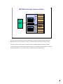
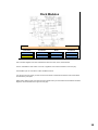
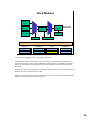
Module Introduction Purpose • This training module covers 68K/ColdFire System Integration Objectives Describe the System Integration Modules. Explain the features of the EPORT & External Interrupts. Describe the ColdFire Interrupt Controller and how it is implemented. Explain the various implementations of clock modules on ColdFire standard products, which include a Phase Lock Loop (PLL). Describe the Power Management Module (PMM) . Explain the features of the Background Debug Module (BDM). Content • 15 pages • 4 questions Learning Time • 25 minutes This module introduces you to Coldfire System Integration which covers the integration of external memory & external interrupts, clock generation, power management, and debug. In this module, we will discuss the System Integration Modules, the features of the EPORT & External Interrupts, as well as the ColdFire Interrupt Controller and how it is implemented. We will also touch on the various implementations of clock modules on ColdFire standard products and the Power Management Module (PMM) and its features. We will conclude with an explanation of the Background Debug Module (BDM). 1 System Integration Module System Bus Controller • Glueless bus interface with chip selects 8-, 16- & 32-bit support for DRAM, SRAM, ROM, FLASH & I/O devices 8 chip-select signals, 2 that are programmable with base address registers, 6 at an offset of one base register Programmable wait states & port sizes IEEE 1149.1 test (JTAG) compliant General purpose I/O interface (the number of I/Os available depends on the device) Programmable interrupt controller Low interrupt latency Up to 7 external interrupt request inputs Interrupt Ctr Chip Selects DRAM Ctr General Purpose I/O The System Integration Module (SIM) contains the System Bus Controller, Interrupt controller, Chip Select controller, DRAM controller and the General Purpose Input/ Output(GPIO) functions. The Chip Select controller provides a glueless interface to most standard DRAMs, SRAMs, ROMs, FLASH, and peripherals. Each of the eight chip select outputs has an address register, mask register, and burst capability. The mask register determines block size, and has the ability to address 8, 16, or 32-bit ports. The chip select outputs feature wait state generation and automatic acknowledge generation. They also feature address setup and address hold features. Memory block sizes range from 64K to two gigabytes of address space. Chip select zero is active out of reset. Normally, this is where the reset vector and boot code reside. Initial parameters for chip select zero are loaded at reset, depending on the state of certain input pins. For example, on the MCF5206e, the state of IRQ1 and IRQ4 determine if chip select zero is an 8, 16, or 32-bit wide port. The SIM also features a parallel I/O port with a number of independent general purpose I/O pins. The number of I/O pins available varies from device to device. Each bit can be programmed individually as either an input pin or an output pin. Sometimes the pins have alternate functions. For example, they may be multiplexed with some debugging signals or upper address lines. The next peripheral we’ll look at is the interrupt controller. It has up to seven external interrupt pins. External Interrupts can be programmed to individual interrupt requests at levels one, four, and seven. Level seven is non-maskable. Internal interrupts can be programmed to any one of seven levels. No more than four interrupts can be assigned to a given level. Each interrupt at the same level must have a unique priority number from one to four assigned to it. You should not program interrupts to have the same level and priority; otherwise, unpredictable results will occur. [Pronounce “DRAMs” as D-rams”] [Pronounce “SRAMs” as S-rams”] [Pronounce “UART” as U-Art] [Pronounce “SIM” as “Sim”] [Pronounce “I/O” as “I-O”] [Pronounce JTAG as “J-Tag”] [Pronounce “IRQ1” as “I-R-Q-one” and so on] [Pronounce “MCF5206e” as “M-C-F-fifty-two-oh-six-E”] 2 EPORT & Interrupt Controller • Pins can used for either: • Interrupts • GPIO Block Diagram • Supports eight sources of external interrupts • Interrupt Sensitivity • Edge Sensitivity • Low-Level Sensitivity • Edge Sensitivity • Rising edge • Falling edge • Both • Schmitt-triggers reduce false interrupts • Operates in all three low-power modes. The Edge Port (EPORT) is a collection of seven pins that can be used as interrupt pins or GPIO pins. When used as an external interrupt each of the seven pins can be individually configured for low-level sensitivity or edge-detecting sensitivity. When edge sensitivity is selected, the edge can be specified as rising edge, falling edge, or both edges. Alternatively, the pin’s interrupt capability can be disabled, turning the pin into a General-Purpose I/O (GPIO) pin. Schmitt trigger logic has been incorporated into the port design so that, when configured for edge sensitivity, false interrupts are avoided on slow rise/fall time transitions. The EPORT is totally functional in either DOZE or WAIT modes of low-power operation, and in fact can be used to bring the processor out of either mode. The same is true in STOP mode except that, since all internal clocks are disabled, the EPORT loses the capability to sync on edge-triggered interrupts and thus only level-sensitive interrupts can be sensed in this mode of operation. Click the Block Diagram button to see a block diagram of the EPORT. 3 EPORT Block Diagram C STOP MODE EPPAR[2n, 2n+1] EDGE DETECT LOGIC D0 EPFR[n] Q D0 D1 Q D1 TO INTERRUPT CONTROLLER IPBUS EPPDR[n] RISING EDGE OF CLOCK EPIER[n] EPDR[n] IRQx PIN EPDDR[n] This block diagram shows that the EPORT is a 7-pin port with built-in flexibility to configure each pin individually as an interrupt pin or a standard digital input or output pin. The EPORT is configured and controlled by accessing six registers. 4 Question True or false? When used as an external interrupt each of the seven pins on the Edge Port (EPORT) can be individually configured for low-level sensitivity or edgedetecting. Click the correct answer and then click Done. A) True B) False Done Take a moment to answer this question about the interrupt controller. Correct! When used as an external interrupt each of the seven pins on the Edge Port (EPORT) can be individually configured for low-level sensitivity or edge-detecting. Click the forward arrow to continue on to the next page. 5 MCF5249 Interrupt Implementation Timer 1-2 DMA 0-3 Primary Interrupt ICR 0-11 Controller IPR IMR ColdFire Core IPL[2:0] Priority decoder Secondary Interrupt IntPri 1-8 Controller Int. Base Spur Int SW Interrupts UART 1-2 WatchDog IIC 1 QSPI Audio Modules MS/SD GPIO IIC 2 A/D Now, let’s consider the MCF5249’s interrupt implementation. Unlike previous ColdFire standard products, the MCF5249 offers two interrupt controllers: the Primary interrupt controller and Secondary interrupt controller. The primary interrupt controller offers the same functionality as the MCF5307/MCF5407 interrupt controller. The Secondary interrupt controller offers additional interrupts for on-chip peripheral devices that are not present in the MCF5307/MCF5407, such as the GPIO, ADC, and additional modules on the MCF5249. 6 5 ColdFire Interrupt Controller • • • • • • • Up to 63 interrupt sources per controller Organized as 7 levels with up to 9 priorities within each level Each source has its own unique vector Global masking and per source masking and forcing capability Hardware masking assist for software management of nested interrupts Simple, register-based interrupt mask set and clear mechanism 1024-byte vector table The ColdFire Interrupt Controller (INTC) supports up to 63 interrupt sources per controller: There are 56 fully-programmable interrupt sources and 7 fixed-level interrupt sources. It is organized as 7 levels with each level supporting up to 9 prioritized requests. Each source has its own unique vector in the exception table. Global masking as well as per source masking capability and Force capability are available. The interrupt controller also supports nested interrupts. Register based mask, set, and clear mechanism are provided for each interrupt source. The vector table contains 256 exception vectors; the first 64 are defined by Freescale the remaining 192 are user-defined interrupt vectors. 7 Clock Modules • Each family of parts has a different generation of clock module subsystems • Please reference the user manual for the part in question for more detail www.freescale.com/coldfire Select a button to learn about the features and to see block diagrams of the following clock modules. 523x, 5270/1, 5274/5 Clock Module 528x, 5214/6 Clock Module 5211/2/3 Clock Module 5207/8, 532x, 537x Clock Module Features Features Features Features Block Diagram Block Diagram Block Diagram Block Diagram Each family of ColdFire standard products implements a clock module that consists of a phase-locked loop, an oscillator circuit for driving an external crystal oscillator, and an on-chip oscillator. The product reference manuals provide more detailed information. They can be accessed at www.freescale.com/coldfire Select a button to learn about the features and to see block diagrams of the clock modules. After you have viewed all of the features and block diagrams, click the forward arrow to go to the next page. 8 Clock Modules Features of the clock module include: – 8- to 25-MHz reference oscillator – Current controlled oscillator range from 50 MHz to 150/166 MHz – Reduced Frequency Divider for reduced frequency operation without forcing the PLL to re-lock – Programmable frequency modulation – Support for low-power modes – Self-clocked Mode operation – Separate clock out signal Select a button to learn about the features and to see block diagrams of the following clock modules. 523x, 5270/1, 5274/5 Clock Module 528x, 5214/6 Clock Module 5211/2/3 Clock Module 5207/8, 532x, 537x Clock Module Features Features Features Features Block Diagram Block Diagram Block Diagram Block Diagram These three families of devices share a common clock module. Although they share a common clock module, the 5274/5 devices run at a faster frequency of 166 MHz than the 523x and 5270/1 devices, which run at 150 MHz. Also, it should be noted that bus frequency is half the core frequency. When using the PLL, the reference clock can range from 8 to 25 MHz. If using the PLL in 1:1 mode, the input clock can range from 24 to 75 MHz for the 523x and 5270/1 devices, and from 24 to 83 MHz for the 5474/5 devices. The PLL can also be bypassed altogether. Using different combinations of the Multiplication Factor Divider (MFD) and Reduced Frequency Divider (RFD), the PLL can synthesize core frequencies as low as 1/32 of the reference clock, or as high as 18x the reference clock. This clock module has an internal Current Controlled Oscillator that runs at a frequency of 50 to 150 MHz for the 523x and 5270/1, and 50 to 166 MHz for the 5274/5. This is what the output of the PLL is generated from. The RFD can be changed (thus changing the output of the PLL) without requiring the PLL to re-lock. In order to reduce EMI, frequency modulation can be used, which spreads the energy of the clock over a broader frequency spectrum. This PLL allows you to modulate the frequency by +/- 1 or 2%. Three low power modes of operation are supported. Wait Mode only stops the CPU and memory clocks until a wakeup event is detected. Doze Mode affects the CPU in the same manner except that you control how each peripheral operates. Control is possible on a module by module basis. In Stop Mode, all clocks to the system are stopped with the exception of the OSC and PLL, and the peripherals cease operation. This is the lowest power mode. These devices can run off an internal clock, in Self-clocked mode, at a range of 10.25 to 15.25 MHz. The clock out signal is different than the core clock. As stated before, the clock out signal is the same as the bus clock, which is half of the core frequency. Select another button to learn more about the clock modules. After you have viewed all of the features and block diagrams, click the forward arrow to go to the next page. 9 Clock Modules STPMD Select a button to learn about the features and to see block diagrams of the following clock modules. 523x, 5270/1, 5274/5 Clock Module 528x, 5214/6 Clock Module 5211/2/3 Clock Module 5207/8, 532x, 537x Clock Module Features Features Features Features Block Diagram Block Diagram Block Diagram Block Diagram This is the block diagram of the clock module that is used in the 523x, 5270/1, 5274/5 devices. The PLL dominates the clock module. If the PLL is bypassed, most of this circuit doesn’t come in to play. The Oscillator input can come from a number of different sources. You can see how much control you have over the clock module on these devices because most of these boxes are controlled by user inputs. Select another button to learn more about the clock modules. After you have viewed all of the features and block diagrams, click the forward arrow to go to the next page. 10 Clock Modules Features of the clock module include: – Crystal amplifier and oscillator – Phase-locked loop – Support for low-power modes – Separate clock out signal Select a button to learn about the features and to see block diagrams of the following clock modules. 523x, 5270/1, 5274/5 Clock Module 528x, 5214/6 Clock Module 5211/2/3 Clock Module 5207/8, 532x, 537x Clock Module Features Features Features Features Block Diagram Block Diagram Block Diagram Block Diagram These two families of devices share a common clock module. Although they share a common clock module, the 528x devices can run at a faster frequency, up to 80 MHz, than the 5214/6 devices, which run at 66 MHz. When using the PLL, the reference clock can range from 2 to 10 MHz. If using the PLL in 1:1 mode, the input clock can range from 33 to 66 MHz for the devices running up to 66 MHz, and 33 to 80 MHz for the devices running up to 80 MHz. The PLL can also be bypassed altogether. Using different combinations of the Multiplication Factor Divider (MFD) and Reduced Frequency Divider (RFD), the PLL can synthesize core frequencies as low as 1/32 of the reference clock, or as high as 18x the reference clock. The RFD can be changed, thus changing the output of the PLL, without requiring the PLL to re-lock. Three low power modes of operation are supported. Wait Mode only stops the CPU and memory clocks until a wakeup event is detected. Doze Mode affects the CPU in the same manner except that you control how each peripheral operates. Control is possible on a module by module basis. In Stop Mode, all clocks to the system are stopped and the peripherals cease operation. This is the lowest power mode. On this clock module, unlike the previous clock module, the clock out signal is equal to the core clock. Select another button to learn more about the clock modules. After you have viewed all of the features and block diagrams, click the forward arrow to go to the next page. 11 Clock Modules Select a button to learn about the features and to see block diagrams of the following clock modules. 523x, 5270/1, 5274/5 Clock Module 528x, 5214/6 Clock Module 5211/2/3 Clock Module 5207/8, 532x, 537x Clock Module Features Features Features Features Block Diagram Block Diagram Block Diagram Block Diagram This is the block diagram of the clock module that is used in these devices. This PLL is very similar to the PLL we just saw on the 523x, 5270/1 and 5274/5 devices, therefore most of the functionality is the same. As a quick reminder: The PLL is the main portion of the clock module, and if the PLL is bypassed, most of this circuit is not used. The clock input can come from a wide array of sources. You have complete control over the entire clock module with all of the different configuration options. Notice the ability to turn ON/OFF the OSC and PLL blocks in Stop Mode. Select another button to learn more about the clock modules. After you have viewed all of the features and block diagrams, click the forward arrow to go to the next page. 12 Clock Modules Features of the clock module include the following: – System can be clocked from PLL or directly from crystal oscillator or relaxation oscillator – 1- to 16-MHz crystal, 8-MHz on-chip relaxation oscillator, or external oscillator reference options – 2- to 10-MHz reference crystal oscillator for normal PLL mode – Support for low-power modes – Separate clock out signal – 2n (0≤n≤15) low-power divider for extremely low frequency operation Select a button to learn about the features and to see block diagrams of the following clock modules. 523x, 5270/1, 5274/5 Clock Module 528x, 5214/6 Clock Module 5211/2/3 Clock Module 5207/8, 532x, 537x Clock Module Features Features Features Features Block Diagram Block Diagram Block Diagram Block Diagram This clock module provides you the option of using either an external crystal, the internal oscillator, or an external oscillator as the reference clock source. In 1:1 mode the user can provide the module crystal reference values in the range of 116MHz. When using normal PLL mode, the crystal reference must be between 2 and 10 MHz. Support is provided for various low power modes such as the ability to enable or disable clocks locally at the module level, as well as providing an external CLKOUT signal to support systems while the module is in low power mode. The external clock signal provided reflects the same state of the internal clocks. The low power divider allows the user to drive the system clock down by a factor of 2n to conserve power. This feature is available regardless of the user supplying a crystal reference or PLL clock to drive the device. Select another button to learn more about the clock modules. After you have viewed all of the features and block diagrams, click the forward arrow to go to the next page. 13 Clock Modules External Crystal Low-Power System Clock External Oscillator Divider PLL On-chip Oscillator Divider REF Select PLL Select Select a button to learn about the features and to see block diagrams of the following clock modules. 523x, 5270/1, 5274/5 Clock Module 528x, 5214/6 Clock Module 5211/2/3 Clock Module 5207/8, 532x, 537x Clock Module Features Features Features Features Block Diagram Block Diagram Block Diagram Block Diagram A block diagram of the MCF5211/12/13 clock modules is shown here. The REF and PLL selection inputs are driven during a device reset. Following reset, the processor boots up according to these options. The PLL usage, multiplication, and division factors can be modified under software control. The clock reference is a static selection that cannot be changed once the options are latched during device reset. The low-power divider is fully programmable and defaults to a division factor of one. The maximum division factor divides the PLL output or reference clock by 32,768. Select another button to learn more about the clock modules. After you have viewed all of the features and block diagrams, click the forward arrow to go to the next page. 14 Clock Modules Features of the clock module include the following: – 16-MHz reference crystal oscillator – Voltage controlled oscillator range from 350 MHz to 540 MHz, resulting in a core frequency of fvco ÷ 2, 3 or 4 (the allowable dividers vary from device to device and the maximum speed is also rated for each device) – Programmable dithering – Direct clocking of system by input clock, bypassing the PLL (LIMP mode) – Loss-of-lock reset Select a button to learn about the features and to see block diagrams of the following clock modules. 523x, 5270/1, 5274/5 Clock Module 528x, 5214/6 Clock Module 5211/2/3 Clock Module 5207/8, 532x, 537x Clock Module Features Features Features Features Block Diagram Block Diagram Block Diagram Block Diagram The PLL clock module on the MCF5208/7, 532x, and 537x device is responsible for generating the core clock frequency and the bus clock. The PLL uses a 16MHz input clock to generate the output core and bus clocks. The VCO range is between 350MHz to 540MHz with a possible divide by 2, 3, or 4 to generate the core frequency. The maximum core frequency and allowable dividers depend on the device. For the MCF5208/7 the VCO divided by 3 and 4 options are supported, where the maximum allowable core frequency is 166.67MHz. For the MCF532x and MCF537x devices only the VCO divided by 2 option is used. The maximum allowable core frequency is 240MHz. The PLL supports dithered operation where output clocks are generated with a frequency that modulates in a triangular waveform with specified percentage of frequency deviation and a specified dither modulation frequency. The dithering deviation can be between 0.75% and 2.5%. The devices also support a LIMP mode. In this mode the PLL is bypassed and the device runs from a factor of the input clock frequency. LIMP mode allows for very low speed operation as a power-savings mode. Finally there is a flag in the reset status register that indicates when the last reset was caused by a PLL loss of lock condition. Select another button to learn more about the clock modules. After you have viewed all of the features and block diagrams, click the forward arrow to go to the next page. 15 Clock Modules Select a button to learn about the features and to see block diagrams of the following clock modules. 523x, 5270/1, 5274/5 Clock Module 528x, 5214/6 Clock Module 5211/2/3 Clock Module 5207/8, 532x, 537x Clock Module Features Features Features Features Block Diagram Block Diagram Block Diagram Block Diagram This is a block diagram of the PLL module used for the MCF5207/8, MCF532x, and MCF537x devices. The equation for the core clock frequency is: Fsys = input clock x (MFD/(4*CPUDIV) The MFD is the programmable divider in the PLL feedback loop. The value specified by the MFD bits establish the multiplication factor applied to the input clock to generate the VCO frequency. The CPUDIV is the output divider used to generate the CPU frequency from the VCO. In addition to the CPU divider there is also a bus clock divider field used to determine the output bus clock frequency. For the MCF5207/8 devices, the bus divider should always be one half of the CPU divider to maintain a fixed 2:1 ratio between the CPU clock and the bus clock. For the MCF532x and MCF537x devices the bus divider is always one third of the CPU divider (fixed 3:1 ratio between the CPU clock and bus clock). Select another button to learn more about the clock modules. After you have viewed all of the features and block diagrams, click the forward arrow to go to the next page. 16 Question Match the clock module with its features by dragging the letters on the left to their appropriate locations on the right. Click Done when you are finished. A 523x, 5270/1, 5274/5 Clock Module D 16-MHz reference crystal oscillator B 528x, 5214/6 Clock Module C 1- to 16-MHz crystal, 8-MHz on-chip relaxation oscillator, or external oscillator reference options C 5211/2/3 Clock Module A 8- to 25-MHz reference oscillator D 5207/8, 532x, 537x Clock Module B Done Reset 2- to 10-MHz reference crystal oscillator Show Solution Take a few minutes now to check your understanding of the clock modules by matching the module with its features. Correct. The correct answers are shown. 17 Standard Power Management Module •Controls the low power operation •Four modes of operation: Run, Wait, Doze, Stop •Run - All modules running •Wait – CPU stopped, all other modules running •Doze - CPU and selected modules stopped •Stop – All modules stopped •Low-power mode wake interrupt level is programmable •Most peripherals can be shutdown Independently The Power Management Module (PMM) controls the low power operation on most of our ColdFire devices. The PMM has four modes of operation: run, wait, doze, and stop. The run mode is the normal system operating mode where current consumption is related directly to the system clock frequency. The wait mode is intended to be used to stop only the CPU and memory clocks until a wakeup event is detected. The doze mode affects the CPU in the same manner as wait mode, except that each peripheral defines individual operation characteristics in doze mode. Finally, the stop mode affects the CPU in the same manner as wait and doze, with the exception that all clocks to the system are stopped and the peripherals cease operation. Exit from a low-power mode can be accomplished via an interrupt, provided that the interrupt priority level is defined. Either fixed or programmable interrupts may be used to exit doze or wait. However, only a fixed (external) interrupt can bring a device out of stop mode. Lastly, another important feature of this module is that it allows the user the ability to shut down most peripherals independently, including the external CLKOUT pin. 18 Enhanced Power Management Module New Features Include: • Distributed clocking allows for module by module clock enable/disable in all operating modes (including RUN mode) • Low power stop modes with programmable options for clock activity • PLL bypass mode for low-speed operation • Low Power Divider Feature • Fixed 8MHz On-Chip Relaxation Oscillator eliminates the need for external crystal Some enhancements to the power management features of the ColdFire families include the addition of module clock gating. This feature allows developers to dynamically stop the clock to selected modules that are not being used in the application. Several low-power modes are provided which allow for incremental control over the clocking of the system. The PLL circuitry may be bypassed in order to reduce system speed, therefore decreasing power consumption. The external clock (EXTAL) is used directly with an optional programmable divider to produce the internal core and bus clocks. Separate from the PLL, the Low Power Divide Module can be enabled in the most power sensitive applications to dynamically divide the clock frequency down below standard levels achieved by the main competitors in the market today. For example, using an 8MHz clock reference with the Low-Power Divide Feature enabled with the maximum divider will produce a system clock of 244 hertz. Lastly, the option to clock the system via the fixed 8MHz On-Chip Relaxation Oscillator eliminates the need for an external crystal. 19 Question What are the four operating modes of the Power Management Module (PMM)? Select all that apply and then click Done. A. B. C. D. E. Doze Ramp Run Stop Wait Done Here’s a question to test your understanding of the Power Management Module. Correct! The PMM has four modes of operation: run, wait, doze, and stop. 20 ColdFire Debug Architecture Real-time trace 4-bit Processor Status (PST) outputs • Instruction complete, taken branch, exception processing, etc. 4-bit Debug DATA outputs (DDATA) • User-defined configuration • Target instruction address on change-of-flow operations – Configurable number of bytes output for instruction addresses • Operand read or write data on internal accesses BDM commands Communication using 3-bit serial, full-duplex channel Read/write CPU registers (only when CPU is halted) Read/write, fill/dump memory (even while CPU is running) The ColdFire solution for real-time trace implements an 8-bit parallel output bus that reports processor execution status and data to an external emulator system. The information displayed on the DDATA lines is configurable. By default, the DDATA lines show the breakpoint status for the processor, but they can be programmed to display other information like branch target addresses and operands. BDM commands are used to communicate between the processor and the third party debugger software. The 17bit BDM command packets are transmitted via a 3-bit serial, full-duplex bus. BDM commands allow a debugger to read or write registers, control registers, and memory. 21 ColdFire Real-Time Debug • Hardware breakpoints: 3 types – – – • Triggers – – • Address Bus ABHR Configurable for 1 or 2 levels Simple AND and OR combinatorial functions ABLR = = Program Counter Data Bus DBR PBR = DBMR PBMR = ƒ Configurable responses: – – • PC mask Operand address high and low match (including attributes) Operand data and mask Force infinite priority debug interrupt Force CPU halt Accessible via the supervisor ISA or the BDM interface TDR1 TDR2 ƒ Trigger Either trigger level can enable some or all of the breakpoints Trigger 2 fires sequentially after trigger 1 fires Either level can invert the meaning of any of the 3 breakpoint matches Next, let’s examine the ColdFire real-time debug. The ColdFire Family provides support debugging real-time applications. For these types of embedded systems, the processor must continue to operate during debug. The debug module provides three types of breakpoints: PC with mask, operand address range, and data with mask. These breakpoints can be configured into one- or two-level triggers. Either trigger level can enable some or all of the breakpoints. Trigger 2 fires sequentially after trigger 1 fires. Either level can invert the meaning of any of the 3 breakpoint matches. Breakpoint hardware can be configured to respond to triggers in several ways via the Trigger Definition Register (TDR). The exact trigger response is also programmable to either halt the CPU or process a debug exception. The existing BDM commands provide access to the processor’s registers and the memory subsystem. The debug module contains registers to support the required functionality. These registers are also accessible from the processor’s supervisor programming model by executing the WDEBUG instruction (write only). Thus, the breakpoint hardware in the debug module can be written by the external development system using the debug serial interface or by the operating system running on the processor core. 22 Question Which of the following are types of breakpoints contained in the Debug module? Select all that apply and then click Done. A. B. C. D. PC with mask Operand Address Range Data with Mask PC without mask Done Take a moment to answer this question about Debug features. Correct! The debug module provides three types of breakpoints: PC with mask, operand address range, and data with mask. 23 Module Summary System Integration Modules EPORT & Interrupt Controller Power Management Module (PMM) Clock Module Background Debug Module (BDM) In this module, you learned about System Integration Modules which contains the System Bus Controller, Interrupt controller, Chip Select controller, DRAM controller and the General Purpose Input/ Output (GPIO) functions. The Edge Port (EPORT) is a collection of seven pins that can be used as interrupt pins individually or GPIO pins. Each interrupt pin can be configured as a level sensitive interrupt pin, an edge detecting interrupt pin (rising, falling edge, or both). If a pin is not needed as input it can be configured as GPIO output. The Power Management Module enables four modes of operation: run, wait, doze, and stop. Most ColdFire peripherals have a control bit that enables the halting of that peripheral when CPU is halted. For example, you can halt a timer system to prevent it from continuing to generate interrupts that may interfere with debugger tool, or you can halt a timer system to prevent it from generating too many interrupt requests when CPU is halted. PLL in a clock module synthesizes the system clocks. The clock module allows the processor to be configured for one of several clocking methods. Clocking modes include internal phase –locked loop clocking with either an external clock reference or an external crystal reference supported by an internal crystal amplifier. The PLL can also be disabled and an external oscillator can be used to clock the device directly. The REF and PLL selection inputs are driven during a device reset. Following reset, the processor boots up according to these options. The PLL usage, multiplication, and division factors can be modified under software control. The clock reference is a static selection that cannot be changed once the options are latched during device reset. The debug module provides three types of breakpoints: PC with mask, operand address range, and data with mask. You’ve learned also about real-time trace possibility and debugging possibility through BDM commands. 24