1
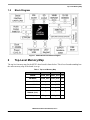
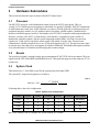
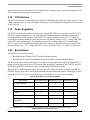
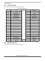
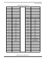
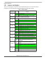
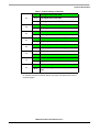
Freescale Semiconductor
User Guide
Rev. 0, 10/2008
M5253 Demo Board User Manual
For M5253 Demo Evaulation/Application Development
by: Shen Li
System Engineer, Shanghai
The M5253 demo board is based on the Freescale V2
architecture family chip, the MCF5253. This board is
shipped with the MCF5253 populated to show the
functionality of this family.
This board is designed as a validation platform with the
maximum flexibility. It serves as a complete
microcomputer system for reference design,
development/evaluation, training, and educational use.
Further more, the board also includes an ethernet
controller on the system FlexBus for debugging and
developing purposes.
© Freescale Semiconductor, Inc., 2008. All rights reserved.
Contents
1
Demo Board Overview . . . . . . . . . . . . . . . . . . . . . . . . . . 2
1.1 Features . . . . . . . . . . . . . . . . . . . . . . . . . . . . . . . . . 2
1.2 Block Diagram . . . . . . . . . . . . . . . . . . . . . . . . . . . . . 3
2
Top-Level Memory Map. . . . . . . . . . . . . . . . . . . . . . . . . . 3
3
Hardware Submodules . . . . . . . . . . . . . . . . . . . . . . . . . . 4
3.1 Processor . . . . . . . . . . . . . . . . . . . . . . . . . . . . . . . . 4
3.2 Resets . . . . . . . . . . . . . . . . . . . . . . . . . . . . . . . . . . . 4
3.3 System Clock. . . . . . . . . . . . . . . . . . . . . . . . . . . . . . 4
3.4 Booting and Programming the Flash/EEPROM Memory . . . . . . . . . . . . . . . . . . . . . . . . . . . . . . . . . . . . . . 5
3.5 SDRAM Interface. . . . . . . . . . . . . . . . . . . . . . . . . . . 6
3.6 BDM Interfaces — Processor . . . . . . . . . . . . . . . . . 6
3.7 USB 2.0 OTG . . . . . . . . . . . . . . . . . . . . . . . . . . . . . 6
3.8 FEC . . . . . . . . . . . . . . . . . . . . . . . . . . . . . . . . . . . . . 7
3.9 ATA . . . . . . . . . . . . . . . . . . . . . . . . . . . . . . . . . . . . . 7
3.10 Interrupts . . . . . . . . . . . . . . . . . . . . . . . . . . . . . . . . 7
3.11 Timers . . . . . . . . . . . . . . . . . . . . . . . . . . . . . . . . . . . 7
3.12 I2C . . . . . . . . . . . . . . . . . . . . . . . . . . . . . . . . . . . . . . 8
3.13 QSPI . . . . . . . . . . . . . . . . . . . . . . . . . . . . . . . . . . . . 8
3.14 RS232 . . . . . . . . . . . . . . . . . . . . . . . . . . . . . . . . . . . 8
3.15 SD Card Interface . . . . . . . . . . . . . . . . . . . . . . . . . . 8
3.16 Audio Interface . . . . . . . . . . . . . . . . . . . . . . . . . . . . 8
3.17 AD Module. . . . . . . . . . . . . . . . . . . . . . . . . . . . . . . . 8
3.18 CAN Interface . . . . . . . . . . . . . . . . . . . . . . . . . . . . . 9
3.19 Power Regulation . . . . . . . . . . . . . . . . . . . . . . . . . . 9
3.20 Boot Options . . . . . . . . . . . . . . . . . . . . . . . . . . . . . . 9
3.21 Serial connector. . . . . . . . . . . . . . . . . . . . . . . . . . . 10
3.22 Parallel connector . . . . . . . . . . . . . . . . . . . . . . . . . 10
3.23 Jumpers and Headers .................................................12
Demo Board Overview
1
Demo Board Overview
1.1
Features
Here is a list of the demo board features. The MCF5253’s external interfaces are:
•
•
•
•
•
•
•
•
•
•
•
•
•
•
•
•
•
•
•
Synchronous serial interface (SSI) connected to the audio codec WM8731
USB support
Stand-alone USB host controller, support-enhanced host-controller interface (EHCI)
USB device mode
USB on-the-go mode including host capability
Supports high-speed (480 Mbps), full-speed (12 Mbps), and low-speed host (1.5Mbps) operations
Supports internal PHY (with UTMI+ interface)
Crystal/clock
On-board BDMTM
ATA interface
MMC/SD interface
Two I2Cs
Four QSPIs
Two CANs
Three UARTs
Six 12-bit resolution ADs
FlexBus with 10/100 ethernet controller
Timers
External interrupts
Memory Subsystems:
• 16-bit width SDRAM
• 2 × 64 KB SRAM
• 8 k on-chip BootROM
• Flash device for boot code development
Power:
• Inputs:
• 5 V (Input to the voltage regulator circuitry)
• Regulated on-board voltages:
— 5 V for USB-VBUS support
— 3.3 V — I/O Voltage
— 1.2 V — CPU-core voltage
M5253 Demo Board User Manual, Rev. 0
2
Freescale Semiconductor
Top-Level Memory Map
1.2
Block Diagram
Figure 1. M5253 Demo Board Block Diagram
2
Top-Level Memory Map
The top-level memory map for the M5253 demo board is shown below. This is best for understanding how
the entire memory map of the board is set up.
Table 1. Top-Level Memory Map
Function
Start Address
SDRAM
0x0000_0000 0x00FF_FFFF 16 MB
SIM MBAR
End Address
0x1000_0000 0x1000_0058
Size
96B
Internal SRAM0
0x2000_0000 0x2000_FFFF 64KB
Internal SRAM1
0x2001_0000 0x2001_FFFF 64KB
SIM MBAR2
0x8000_0000 0x8000_01FF 512B
Ethernet Controller 0xE000_0300 0xE000_03FF
DM9000 (CS1)
FLASH (CS0)
64B
0xFF80_0000 0xFFFF_FFFF 8MB
M5253 Demo Board User Manual, Rev. 0
Freescale Semiconductor
3
Hardware Submodules
3
Hardware Submodules
This section describes the major sections of the M5253 demo board.
3.1
Processor
The MCF5253 processor is the fundamental control chip on the M5253 demo board. This is a
version 2 (V2) ColdFire processor running at a maximum core speed of 140 MHz. MCF5253 implements
an 8 KB instruction cache, three UART channels, two timers, 128 KB of SRAM, a QSPI (queued serial
peripheral interface) module, two I2C modules, three I2S modules, an IDE module, a dedicated ATA
interface with DMA support, two FlexCAN modules, an OTG USB 2.0 controller with integrated physical
interface, real-time clock (RTC), a flash memory stick interface, 60 parallel I/O ports (which are
multiplexed with other signals), and the system integration module (SIM). All of the core-processor
registers are 32 bits wide except for the status register (SR) which is 16 bits wide. This processor
communicates with the external devices over a 16 bits wide data bus, D[31:16]. The processor has a logic
to generate up to four chip selects, and support for a bank of SDRAMs. This board has brought out almost
every silicon feature for evaluation and developing the customer design.
3.2
Resets
The system reset signal is coming from the power management IC MC34702 with a reset button. The reset
signal feeds the CPU, flash, BDM, and DM9000 devices. This signal also appears on the connector J17 for
external use.
3.3
System Clock
This board uses a 11.2896 MHz crystal for the system main clock input CRIN.
The system PLL output-clock equation is as follows:
Eqn. 1
PSTCLK =
Fin ∗×
2 ∗× VCXODIV
PLLDIV ×∗ CPUDIV ×* VCXOOUT
Following table is the clock configuration:
Table 2. System Clock Configuration
Fin (MHz)
CPUDIV
CRSEL
VCXODIV
PLLDIV
VCXOOUT
PSTCLK (MHz)
11.2896
2
0
62
5
1
140 (default)
11.2896
2
0
42
4
1
120
11.2896
3
0
51
4
1
96
11.2896
4
0
51
4
1
72
Here is the example code to configure the system running at 140 MHz:
M5253 Demo Board User Manual, Rev. 0
4
Freescale Semiconductor
Hardware Submodules
…
MCF_CLOCK_PLLCONFIG = 0x1243E054;
MCF_CLOCK_PLLCONFIG = 0x1243E055;
/* Wait for PLL to lock */
while (!(MCF_CLOCK_PLLCONFIG & MCF_CLOCK_PLLCONFIG_LOCK))
;
…
Audio module also uses the 11.2896 MHz frequency for operation, so Faudio = AUDIOCLK = CRIN
(A20/A24 switch pull up, down).
3.4
Booting and Programming the Flash/EEPROM Memory
This demo board includes both a serial boot EEPROM and the program flash memories on-board.
3.4.1
Serial Boot EEPROM
The serial boot EEPROM (AT24C256) can store configuration parameters and the boot code. It is I2C bus
EEPROM and the address is 1010000x (x means R/W#-bit).
When the MCF5253 boot mode is configured as I2C master boot (A23 pull down and GPIO50 = 0,
GPIO49 = 0, GPIO48 = 0) the MCF5253 loads the boot code from the I2C EEPROM at powerup. The
board uses this EEPROM just for a demonstration of the MCF5253’s serial-boot function. There is no
pre-flashed software inside the EEPROM. Customer can put his own boot code there and configure the
data into this device. Please see Table 4 for more details about the serial-boot configuration.
3.4.2
Flash
A 8 MB (4Mx16) flash (SST39VF6401) memory resides on the CS0 space of the FlexBus memory on the
demo board. The software must configure the memory-access parameters to be consistent with the
hardware configuration. The SST39VF6401 is uniformed as 2 Kword sectors, totally in 2 K sectors.
When the MCF5253 boot mode is configured as CS0/CS4 boot (A23 pullup), the CPU loads the code from
the flash at powerup. We intended to reside the dBUG or U-boot as the bootloader at the beginning of the
flash memory.
Flash address
0xFF80_0000 ~ 0xFFFF_FFFF
The CS0 initialization code is below:
…
; CS0 = Flash SST39VF6401B - 8Mbytes
writemem.w 0x10000080
0xFF80
; CSAR0 - FlashBase = 0xFF80_0000 - 0xFFFF_FFFF
writemem.w 0x1000008A
0x0D80
; CSCR0
writemem.l 0x10000084
0x007F0021 ; CSMR0 - 0xFF80_0000 - 0xFFFF_FFFF
…
M5253 Demo Board User Manual, Rev. 0
Freescale Semiconductor
5
Hardware Submodules
3.5
SDRAM Interface
The M5253 demo board provides 16 MB of on-board SDRAM, which is located at 0x0. The on-board
terminations are provided. The software should take notice of the timing configuration of this device for
the SDRAM controller module.
SDRAM address
0x0000_0000 ~ 0x00FF_FFFF
The SDRAM timing characters are listed below:
tRCD > 20 ns
CASL = 2 CLK
45 ns < tRAS < 100 ns
tRP > 20 ns
tRWL, RDL = 1 CLK (less than 100 MHz speed)
Here is the initialization code example for the SDRAM controller:
…
; set up 5253 cpu settings
; initialize memory settings SDRAM base Address 0x0000_0000
writemem.w 0x10000100 0x8209
;SDRAM0 DCR0A
writemem.l 0x10000108 0x00002320 ;SDRAM0 DACR0A
writemem.l 0x1000010C 0x00FC0001 ;SDRAM0 DMR0A
writemem.l 0x10000108 0x00002328 ;SDRAM0 DACR0B
writemem.l 0x00000000 0x00000000 ;SDRAM0 MEMWR0
writemem.l 0x10000108 0x0000A320 ;SDRAM0 DACR0C
writemem.l 0x10000108 0x0000A360 ;SDRAM0 DACR0D
writemem.l 0x00000800 0x00000800 ;SDRAM0 MODE0…
3.6
BDM Interfaces — Processor
The M5253 demo board provides an on-board BDM (background debug mode) module and a connector
(26-pin header) to give the final user the ability to utilize the BDM features of the MCF5253 processor.
With the on-board BDM, the customer can use a USB A-to-B cable for debugging and downloading the
software. The 26-pin header is not populated on the board by default, the customer can populate it on the
J14. To enable the header, the customer also needs to populate four 0 Ω resistors on R4 to R7.
3.7
USB 2.0 OTG
The MCF5253 processor contains a USB high-speed OTG module. This module is USB 2.0 compliant. It
supports both the host and the device modes, and provides an on-chip high-speed/full-speed/low-speed
transceiver. One mini-AB receptacle (USB 2.0 OTG) is provided on the Jamaica board. The board also
provides an external power distribution switch (MIC2026) to provide the VBUS when necessary. The USB
module uses a 24 MHz crystal for module clock.
M5253 Demo Board User Manual, Rev. 0
6
Freescale Semiconductor
Hardware Submodules
When jumpers J32 and J26 are installed, the MIC2026 can output a maximum of 500 mA 5V power to the
VBUS, working in the USB-host mode. When working in the device and otg mode, the J32 and J26 should
be disconnected.
3.8
FEC
The M5253 demo provides a 10/100M ethernet interface by an ethernet controller DM9000 on the CS1 of
the FlexBus. The board also provides the RJ45 connectors with integrated magnetics and LEDs. As there
is no EEPROM for the DM9000 on this board, there is no default MAC address configured for the M5253
demo board. The software takes the response to configure the MAC address of the DM9000 after powerup,
but Freescale has assigned an unique ethernet MAC address for each board and pasted it on the back of the
board. DM9000’s system address is at 0xE000_0300. The address index port is 0xE000_0300 and the data
port is 0xE000_0304. The DM9000’s interrupt pin (active high default) uses the system external interrupt
GPI5. The GPI5 L-H event is the second interrupt at controller number 37.
3.9
ATA
The M5253 demo board provides an ATA connector that interfaces with the MCF5253 processor’s ATA
interface. This board only supports one ATA device on the cable. To support a multi-ATA harddisk, the
CSEL signal on the board must be connected to the GND according to the ATA/ATAPI-6 specification,
because the board does not support it.
A device connected to the ATA interface must be powered by a separate supply (such as a peripheral power
connector provided by the ATX power supply).
3.10
Interrupts
The MCF5253 has a total number of seven external-interrupt input pins GPI0~6. Four of them are
connected to the push-button on the M5253 demo board and they are the GPI1~4’s. The GPI5 is reserved
for the ethernet controller DM9000. The GPI6 is reserved for customer usage. The external interrupt pins
are all multiplexed with other modules.
3.11
Timers
The MCF5253 contains a software watchdog timer and two 16-bit general-purpose timers (GPT).
The software watchdog timer provides a means of preventing the system from lockup due to uncontrolled
software loops via a special software-service sequence.
The two general-purpose timer modules (timer 0 and timer 1) in the MCF5253 can provide two
independent system interrupts, but only timer 1 can provide an output signal as TOUT1. It is multiplexed
with the SDATAO1.
M5253 Demo Board User Manual, Rev. 0
Freescale Semiconductor
7
Hardware Submodules
3.12
I2C
MCF5253 has two I2C modules (I2C0 and I2C1) and is fully compatible with the I2C-bus standard. On the
M5253 demo board, the I2C0 is connected to the EEPROM, the audio codec, and the power manager.
The I2C1 is reserved for customer usage.
Here is a list of the I2C device default addresses on the I2C0.
Table 3. I2C Device Addresses
3.13
I2C Device
I2C address
EEPROM
0b1010000x
WM8731
0b0011010x
MC34702
0b1110111x
QSPI
The MCF5253’s QSPI module has up to seven signals: QSPI_Dout, QSPI_Din, QSPI_CLK, and
QSPI_CS[3:0]. On the M5253 demo board, the QSPI module is not connected to any QSPI device, but is
just routed out at the serial connector.
3.14
RS232
The MCF5253 includes three UART modules. To reduce the board’s dimensions and cost down, we
consider that the three UART’s should share the transceiver and the DB9 connector with the jumpers J12,
J13, J20, and J24.
3.15
SD Card Interface
The MCF5253 has a flash media interface which can interface with the Sony Memory Stick and
Multi-Media Card (MMC)/Secure Digital (SD) flash cards. The M5253 demo board installs an MMC/SD
socket for evaluation and verification.
3.16
Audio Interface
The MCF5253 contains an audio interface module (AIM) which is equipped with three serial-audio
interfaces compliant with the Phillips I2S and Sony EIAJ formats. The M5253 demo reserves an audio
AD/DA IC WM8731 for the audio application development. It is connected to I2S1 by default. The MCLK
signal has a frequency of 11.1896 MHz and comes from the MCF5253. The WM8731 is Wolfson’s
low-power stereo codec with an integrated headphone driver. It implements stereo 24-bit multi-bit
sigma-delta ADCs and DACs with oversampling, digital interpolation, and decimation filters.
3.17
AD Module
The MCF5253 has a 12-bit 6-channel analog-to-digital module. The M5253 demo board provides a 3-axis
accelerator and two potentiometers connected to the ADIN0~4 for demonstration. The analog channels are
M5253 Demo Board User Manual, Rev. 0
8
Freescale Semiconductor
Hardware Submodules
also routed out at the serial connector J17 for customer use. Customer can use the on-board jumpers J5 and
J27 to control the analog input of each channel.
3.18
CAN Interface
The MCF5253 has two CAN-bus interfaces. The M5253 demo board provides one CAN transceiver with
a DB9 connector. There is a 120 Ω loopback load resistor, which represents the impedance of the system
on the CAN bus.
3.19
Power Regulation
The M5253 demo board provides a Freescale QuiccSupply MC34702 power regulator. The MC34702 is
Freescale’s power management IC, which incorporates a high-performance switching regulator and a
low-dropout (LDO) linear-regulator control circuit. This power regulator provides a 3.3 V voltage by
switching the regulator module for the microprocessor I/O and bus voltage and 1.2 V voltage from LDO
for the CPU-core voltage supply. The regulator generates these voltages from a 5 V external supply.
The 5 V supply can be provided through the power-jack connector. The MCF5253 has an internal LDO
that can also generate a 1.2 V voltage and the J15 is to select which of the 1.2 V voltages is to be used.
3.20
Boot Options
The MCF5253 has two boot options:
• Booting from the FlexBus CS0/CS4 with default boot options.
• Booting from the internal bootROM and override defaults with the serial-boot facility.
The boot mode is determined by the logic level of the pin A23 during the powerup reset. When the A23 is
pulled up during the powerup, the CPU will boot from the memory connected to the CS0/CS4, which is
the flash on the M5253 demo board. The J21 on the board selects the boot option.
When the A23 is pulled down during the powerup, the CPU will boot from the on-chip boot ROM. The
GPIO48~50 pin’s logic will be sensed at the powerup to decide further boot options. On the M5253 demo
board, the J29, J31, and J30 are to select the logic of the GPIO48~50. Here is the boot table:
Table 4. Boot Options of the On-Chip ROM
BOOT MODE
GPIO50/PST0 (J30) GPIO49/PST1 (J31) GPIO48/PST2 (J29)
*I2C master (default)*
0
0
0
SPI master
0
0
1
IDE master
0
1
0
I2C slave
1
0
0
UART (5.6448/11.2896 MHz)
1
0
1
UART (8.4672/16.9344/
33.8688 MHz)
1
1
0
UART (5/10/20 MHz)
1
1
1
* - means default setting, 0 - means the signal to be pulled to ground, 1 - means the signal to be pulled high
M5253 Demo Board User Manual, Rev. 0
Freescale Semiconductor
9
Hardware Submodules
3.21
Serial Connector
Table 5 is the signal definition of the serial connector J17.
Table 5. Serial Connector J17
3.22
1
3.3 V
2
CTS0#/IRQ4/GPI3
3
GND
4
5V
5
TXD0/GPIO45
6
RSTO
7
RXD0/GPIO46
8
CTS1#/IRQ2/GPI1
9
SDATAI1/GPIO17
10
EBUIN1/GPIO36
11
SDATAO1/GPIO18
12
EBUIN2/GPIO13
13
LRCK1/GPIO19
14
EBUIN3/GPIO14
15
SCLK1/GPIO20
16
EBUOUT1/GPIO37
17
QSPI_OUT/GPIO27
18
SDATAO2/GPIO34
19
QSPI_DIN/GPIO26
20
LRCK2/GPIO23
21
QSPI_CLK/GPIO25
22
SCLK2/GPIO22
23
QSPI_CS0/GPIO15
24
SDATAI3/GPIO8
25
QSPI_CS1/GPIO16
26
SCL1/TXD1/GPIO10
27
QSPI_CS2/MCLK2/GPIO24
28
SDA1/RXD1/GPIO44
29
LRCK3/GPIO43
30
SCLK3/GPIO35
31
TXD2/IRQ1/GPI0
32
MCLK1/GPIO11
33
RTS1#/IRQ3/GPI2
34
AN0/GPI52
35
RTS0#/IRQ5/GPI4
36
AN1/GPI53
37
RXD2/IRQ7/GPI6
38
AN2/GPI54
39
PSTCLK/GPIO51
40
AN3/GPI55
41
AN5/GPI57
42
AN4/GPI56
Parallel Connector
Table 6 is the signal definition of the parallel connector J34.
M5253 Demo Board User Manual, Rev. 0
10
Freescale Semiconductor
Hardware Submodules
Table 6. Parallel Connector J34
1
3.3 V
2
A1
3
GND
4
A2
5
A3
6
A4
7
A5
8
A6
9
A7
10
A8
11
A9
12
A10
13
A11
14
A12
15
A13
16
A14
17
A15
18
A16
19
A17
20
A18
21
A19
22
A20/A24
23
A21
24
A22
25
A23/GPIO54
26
D16
27
D17
28
D18
29
D19
30
D20
31
D21
32
D22
33
D23
34
D24
35
D25
36
D26
37
D27
38
D28
39
D29
40
D30
41
D31
42
RW
43
OE#
44
CFLG/IRQ6/GPI5
45
RSTO
46
BCLK/GPIO40
47
TA#/GPIO12
48
IDE_DIOR#/GPIO31
49
IDE_DIOW#/GPIO32
50
IDE_IORDY#/GPIO33
51
CS0#/CS4#
52
CS1#/GPIO28
53
BUFENB1#/GPIO29
54
BUFENB2#/GPIO30
55
WAKEUP#/GPIO21
56
PST3/GPIO47
57
PST2/GPIO48
58
PST1/GPIO49
59
PST0/GPIO50
60
GND
M5253 Demo Board User Manual, Rev. 0
Freescale Semiconductor
11
Hardware Submodules
3.23
Jumpers and Headers
There are several jumpers on the M5253 demo board that allow the user to control the hardware
configuration. The following table provides descriptions for all the jumper settings.
Table 7. Jumper Settings
Reference
Designator
Setting12
*1:2*
Function
BOOT from CS0
J21
2:3
J29,J30,J31
BOOT from internal ROM(for serial bus boot)
Refer Table 4 for detail(no shunt default)
1:2
Audio CLK from LRCK3 PIN
J16
*2:3*
ON
Audio CLK from CRIN PIN
USB host enable
J26,J32
*OFF*
ON
USB device/otg mode
I2C0/SDATA pin use for SD socket function
J25
*OFF*
I2C0/SDATA pin not use for SD socket function
*ON*
I2C0/SDATA pin use for I2C0
OFF
I2C0/SDATA pin not use for I2C0
*ON*
WM8731 MCLK come from MCLK2 of MCF5253
OFF
WM8731 MCLK come from the on crystal beside
J23
J10
2× *ON* AD 0,1 input from on board potentiometer
J5(2x2)
OFF
AD 0,1 not input from on board potentiometer
3× *ON* AD 2,3,4 input from on board 3-axis accelerator
J27(2x3)
OFF
AD 2,3,4 not input from on board 3-axis
accelerator
ON
BUFEN1# and TXD2 used for GPIO for SD
socket
J7(2x2)
*OFF*
J24
BUFEN1# and TXD2 not used for GPIO for SD
socket
*1:2*
RXD signal come from RXD0
3:4
RXD signal come from RXD1
5:6
RXD signal come from RXD2
M5253 Demo Board User Manual, Rev. 0
12
Freescale Semiconductor
Hardware Submodules
Table 7. Jumper Settings (continued)
J13
*1:2*
TXD signal come from TXD0
3:4
TXD signal come from TXD1
5:6
TXD signal come from TXD2
*1:2*
RTS# signal come from RTS0#
3:4
RTS# signal come from RTS1#
*1:2*
CTS# signal come from CTS0#
3:4
CTS# signal come from CTS1#
J20
J12
*1:2*
CANTX signal come from CAN0_TX
3:4
CANTX signal come from CAN1_TX
*1:2*
CANRX signal come from CAN0_RX
3:4
CANRX signal come from CAN1_RX
ON
CAN bus termintor 120ohm connected
J14
J18
J8
*OFF*
*1:2*
CAN bus termintor 120ohm unconnected
5v input come from power jack
J6
2:3
*1:2*
1.2 V core voltage come from power manage IC
2:3
1.2 V core voltage come from MCF5253 internal
LDO
J15
1
2
5v input come from the BDM module
* indicates the default setting
On indicates that a shunt should be fitted on the jumper; Off indicates that no shunt
should be applied
M5253 Demo Board User Manual, Rev. 0
Freescale Semiconductor
13
How to Reach Us:
Home Page:
www.freescale.com
Web Support:
http://www.freescale.com/support
USA/Europe or Locations Not Listed:
Freescale Semiconductor, Inc.
Technical Information Center, EL516
2100 East Elliot Road
Tempe, Arizona 85284
+1-800-521-6274 or +1-480-768-2130
www.freescale.com/support
Europe, Middle East, and Africa:
Freescale Halbleiter Deutschland GmbH
Technical Information Center
Schatzbogen 7
81829 Muenchen, Germany
+44 1296 380 456 (English)
+46 8 52200080 (English)
+49 89 92103 559 (German)
+33 1 69 35 48 48 (French)
www.freescale.com/support
Japan:
Freescale Semiconductor Japan Ltd.
Headquarters
ARCO Tower 15F
1-8-1, Shimo-Meguro, Meguro-ku,
Tokyo 153-0064
Japan
0120 191014 or +81 3 5437 9125
[email protected]
Asia/Pacific:
Freescale Semiconductor China Ltd.
Exchange Building 23F
No. 118 Jianguo Road
Chaoyang District
Beijing 100022
China
+86 10 5879 8000
[email protected]
For Literature Requests Only:
Freescale Semiconductor Literature Distribution Center
P.O. Box 5405
Denver, Colorado 80217
1-800-441-2447 or 303-675-2140
Fax: 303-675-2150
[email protected]
Document Number:
Rev. 0
10/2008
Information in this document is provided solely to enable system and software
implementers to use Freescale Semiconductor products. There are no express or
implied copyright licenses granted hereunder to design or fabricate any integrated
circuits or integrated circuits based on the information in this document.
Freescale Semiconductor reserves the right to make changes without further notice to
any products herein. Freescale Semiconductor makes no warranty, representation or
guarantee regarding the suitability of its products for any particular purpose, nor does
Freescale Semiconductor assume any liability arising out of the application or use of any
product or circuit, and specifically disclaims any and all liability, including without
limitation consequential or incidental damages. “Typical” parameters that may be
provided in Freescale Semiconductor data sheets and/or specifications can and do vary
in different applications and actual performance may vary over time. All operating
parameters, including “Typicals”, must be validated for each customer application by
customer’s technical experts. Freescale Semiconductor does not convey any license
under its patent rights nor the rights of others. Freescale Semiconductor products are
not designed, intended, or authorized for use as components in systems intended for
surgical implant into the body, or other applications intended to support or sustain life,
or for any other application in which the failure of the Freescale Semiconductor product
could create a situation where personal injury or death may occur. Should Buyer
purchase or use Freescale Semiconductor products for any such unintended or
unauthorized application, Buyer shall indemnify and hold Freescale Semiconductor and
its officers, employees, subsidiaries, affiliates, and distributors harmless against all
claims, costs, damages, and expenses, and reasonable attorney fees arising out of,
directly or indirectly, any claim of personal injury or death associated with such
unintended or unauthorized use, even if such claim alleges that Freescale
Semiconductor was negligent regarding the design or manufacture of the part.
RoHS-compliant and/or Pb-free versions of Freescale products have the functionality
and electrical characteristics as their non-RoHS-compliant and/or non-Pb-free
counterparts. For further information, see http://www.freescale.com or contact your
Freescale sales representative.
For information on Freescale’s Environmental Products program, go to
http://www.freescale.com/epp.
Freescale™ and the Freescale logo are trademarks of Freescale Semiconductor, Inc.
All other product or service names are the property of their respective owners.
© Freescale Semiconductor, Inc. 2008. All rights reserved.