1
Design and implementation of a
prototype platform for evolution in
materio
Odd Rune Strømmen Lykkebø
Master of Science in Computer Science
Submission date: July 2010
Supervisor:
Gunnar Tufte, IDI
Norwegian University of Science and Technology
Department of Computer and Information Science
Problem Description
The fact that silicon is a material that can be exploited to implement
powerful electronic circuits capable of computation is well known. Design
of computational machines in silicon follow a top down design metrology,
this metrology enables circuit designers to abstract away from the actual
properties of the material. Designers deal with transistors at wires at
one level, gates at a higher level, modules at a even higher level and a
top architecture, e.g. micro architecture.
Evolution in Materio in contrast explores a bottom up approach. The goal
exploit the basic computational properties of
materials. Such an approach require a search, e.g. by an Evolutionary
Algorithm (EA), to identify eventual computation properties that may be
inherent in a material. We believe that materials that can "compute", and
that this computation can be identified, most likely do computation by
emergent behaviour.
Early work has looked into e.g. liquid crystal and solution of metallic
ions. To be able to explore possible computational properties of materials
a flexible experimental platform is needed. In this first attempt a micro
electrode array is suggested as the interface between the material under
investigation and world. The world here is IO to sensors and actuators and
an interface to the machine running an EA to configure the material.
To accomplish such a system a prototype platform most be designed. The
design includes hardware and software needed to electrically interface the
micro electrode array, a flexible bridge between a host machine running
the EA and the material bay.
Assignment given: 03. March 2010
Supervisor: Gunnar Tufte, IDI
is to investigate and
Abstract
Evolution in-materio is a relatively new field in which one seeks to reach beyond
the common transistor as a basic building block for computing entities by exploiting the physical properties of materials through evolution. This thesis details the
design and implementation of a general platform for material exploration. It also
demonstrates the functionality of the platform with experiments run with air as
the material under test.
Preface
This project was done during the spring and early summer of 2010 at the Institute
of Information and Computer science (IDI) at NTNU, as the final step towards
my Master of Technology degree.
Acknowledgements
A great thanks to my supervisor, Gunnar Tufte, whose engineering experience
and support has been a great help during this project. Further thanks goes to
Julian Miller for valuable input.
I would also like to show gratitude to my brothers-in-arms at our office, and
especially thank Kjeftil Oftedal for invaluable help when chasing strange hardware bugs.
Odd Rune, July 2010.
3
Contents
1 Introduction
1
2 Background
2.1 Dealing with complexity . . . . . . . . . . . .
2.2 Intrinsic hardware evolution . . . . . . . . . .
2.2.1 Thompson’s experiment . . . . . . . .
2.2.2 Lindens antenna . . . . . . . . . . . .
2.2.3 Fault tolerance . . . . . . . . . . . . .
2.3 Exploiting materials . . . . . . . . . . . . . .
2.3.1 Gordon Pask . . . . . . . . . . . . . .
2.4 Evolution in Materials . . . . . . . . . . . . .
2.4.1 Field programmable matter array . . .
2.4.2 The evolvable motherboard . . . . . .
2.4.3 Liquid Crystal Evolvable Motherboard
.
.
.
.
.
.
.
.
.
.
.
.
.
.
.
.
.
.
.
.
.
.
.
.
.
.
.
.
.
.
.
.
.
.
.
.
.
.
.
.
.
.
.
.
.
.
.
.
.
.
.
.
.
.
.
.
.
.
.
.
.
.
.
.
.
.
.
.
.
.
.
.
.
.
.
.
.
.
.
.
.
.
.
.
.
.
.
.
.
.
.
.
.
.
.
.
.
.
.
.
.
.
.
.
.
.
.
.
.
.
.
.
.
.
.
.
.
.
.
.
.
.
.
.
.
.
.
.
.
.
.
.
.
.
.
.
.
.
.
.
.
.
.
.
.
.
.
.
.
.
.
.
.
.
.
.
.
.
.
.
.
.
.
.
.
.
.
.
.
.
.
.
.
.
.
.
.
.
.
.
.
.
.
.
.
.
.
.
.
.
.
.
.
.
.
.
.
.
3
4
4
5
5
5
6
6
7
8
8
9
3 System overview
3.1 Host computer . . .
3.2 Material Bay (MB) .
3.3 Mecobo . . . . . . .
3.4 A complete example
.
.
.
.
.
.
.
.
.
.
.
.
.
.
.
.
.
.
.
.
.
.
.
.
.
.
.
.
.
.
.
.
.
.
.
.
.
.
.
.
.
.
.
.
.
.
.
.
.
.
.
.
.
.
.
.
.
.
.
.
.
.
.
.
.
.
.
.
.
.
.
.
13
13
15
15
16
4 Design and implementation details
4.1 System parts . . . . . . . . . . . . . . . . . . .
4.2 Design . . . . . . . . . . . . . . . . . . . . . . .
4.3 Hardware implementation . . . . . . . . . . . .
4.3.1 PCB . . . . . . . . . . . . . . . . . . . .
4.3.2 Version 2 . . . . . . . . . . . . . . . . .
4.4 HDL . . . . . . . . . . . . . . . . . . . . . . . .
4.4.1 Toplevel . . . . . . . . . . . . . . . . . .
4.4.2 Memory controller and shared memory .
4.4.3 Pin controller . . . . . . . . . . . . . . .
4.4.4 User module . . . . . . . . . . . . . . .
4.5 Microcontroller . . . . . . . . . . . . . . . . . .
4.5.1 The Atmel driver framework . . . . . .
4.5.2 Peripheral setup . . . . . . . . . . . . .
4.6 Host computer: libEMB . . . . . . . . . . . . .
.
.
.
.
.
.
.
.
.
.
.
.
.
.
.
.
.
.
.
.
.
.
.
.
.
.
.
.
.
.
.
.
.
.
.
.
.
.
.
.
.
.
.
.
.
.
.
.
.
.
.
.
.
.
.
.
.
.
.
.
.
.
.
.
.
.
.
.
.
.
.
.
.
.
.
.
.
.
.
.
.
.
.
.
.
.
.
.
.
.
.
.
.
.
.
.
.
.
.
.
.
.
.
.
.
.
.
.
.
.
.
.
.
.
.
.
.
.
.
.
.
.
.
.
.
.
.
.
.
.
.
.
.
.
.
.
.
.
.
.
.
.
.
.
.
.
.
.
.
.
.
.
.
.
.
.
.
.
.
.
.
.
.
.
.
.
.
.
.
.
.
.
.
.
.
.
.
.
.
.
.
.
.
.
.
.
.
.
.
.
.
.
.
.
.
.
.
.
.
.
.
.
.
.
.
.
.
.
.
.
.
.
.
.
.
.
.
.
.
.
.
.
.
.
.
.
.
.
.
.
.
.
.
.
.
.
.
.
19
19
20
21
24
26
26
26
26
29
32
34
34
34
37
.
.
.
.
.
.
.
.
.
.
.
.
.
.
.
.
.
.
.
.
.
.
.
.
.
.
.
.
.
.
.
.
.
.
.
.
.
.
.
.
i
.
.
.
.
.
.
.
.
.
.
.
.
.
.
.
.
.
.
.
.
.
.
.
.
.
.
.
.
.
37
39
39
40
43
43
43
44
44
45
46
46
46
.
.
.
.
.
.
.
.
.
.
.
.
.
.
.
.
.
49
49
49
50
50
51
51
51
51
51
52
52
52
52
53
53
54
54
.
.
.
.
55
55
55
56
56
7 Experiment results
7.1 Experimental results . . . . . . . . . . . . . . . . . . . . . . . . . . . . . . . .
7.1.1 Static genome . . . . . . . . . . . . . . . . . . . . . . . . . . . . . . . .
7.1.2 4 + 1 EA . . . . . . . . . . . . . . . . . . . . . . . . . . . . . . . . . .
59
59
59
60
8 Conclusion
8.1 The future . . . . . . . . . . . . . . . . . . . . . . . . . . . . . . . . . . . . . .
65
66
4.7
4.8
4.9
4.6.1 Structures in libEMB . . . . . . . . . . . . . .
4.6.2 Translating between patterns and configuration
Microcontroller program . . . . . . . . . . . . . . . . .
4.7.1 Microcontroller commands . . . . . . . . . . . .
4.7.2 Response mechanism and error codes . . . . . .
Communication between host and microcontroller . . .
4.8.1 The Mecobo communication stack . . . . . . .
Discussion . . . . . . . . . . . . . . . . . . . . . . . . .
4.9.1 System design . . . . . . . . . . . . . . . . . . .
4.9.2 Component selection . . . . . . . . . . . . . . .
4.9.3 PCB . . . . . . . . . . . . . . . . . . . . . . . .
4.9.4 HDL . . . . . . . . . . . . . . . . . . . . . . . .
4.9.5 libEMB and µC software . . . . . . . . . . . .
5 Testing and board evaluation
5.1 Connectivity . . . . . . . . . . . .
5.1.1 Beep-testing . . . . . . . . .
5.1.2 Shared memory . . . . . . .
5.1.3 Pin headers . . . . . . . . .
5.1.4 Host to board . . . . . . . .
5.1.5 Results of connectivity tests
5.2 Component tests . . . . . . . . . .
5.3 System tests . . . . . . . . . . . . .
5.3.1 Functional tests of libEMB
5.3.2 Performance . . . . . . . .
5.3.3 Performance results . . . .
5.4 FPGA design tests . . . . . . . . .
5.4.1 Testing procedure . . . . .
5.4.2 Static memory controller .
5.4.3 Pin controller . . . . . . . .
5.4.4 User module . . . . . . . .
5.4.5 Toplevel . . . . . . . . . . .
.
.
.
.
.
.
.
.
.
.
.
.
.
.
.
.
.
6 Experimental methodology
6.1 Initial experiments in air . . . . . . .
6.1.1 Experimental setup . . . . . .
6.1.2 Static genomes . . . . . . . .
6.1.3 4+1 Evolutionary Algorithm
.
.
.
.
.
.
.
.
.
.
.
.
.
.
.
.
.
.
.
.
.
.
.
.
.
.
.
.
.
.
.
.
.
.
.
.
.
.
.
.
.
.
.
.
.
.
.
.
.
.
.
.
.
.
.
.
.
.
.
.
.
.
.
.
.
.
.
.
.
.
.
.
.
.
.
.
.
.
.
.
.
.
.
.
.
.
.
.
.
.
.
.
.
.
.
.
.
.
.
.
.
.
.
.
.
.
.
.
.
.
.
.
.
.
.
.
.
.
.
.
.
.
.
.
.
.
.
.
.
.
.
.
.
.
.
.
.
.
.
.
.
.
.
.
.
.
.
.
.
.
.
.
.
.
.
.
.
.
.
.
.
.
.
.
.
.
.
.
.
.
.
.
.
.
.
.
.
.
.
.
.
.
.
.
.
.
.
.
.
.
.
.
.
.
.
.
.
.
.
.
.
.
.
.
.
.
.
.
.
.
. . . . . . .
byte arrays
. . . . . . .
. . . . . . .
. . . . . . .
. . . . . . .
. . . . . . .
. . . . . . .
. . . . . . .
. . . . . . .
. . . . . . .
. . . . . . .
. . . . . . .
.
.
.
.
.
.
.
.
.
.
.
.
.
.
.
.
.
.
.
.
.
.
.
.
.
.
.
.
.
.
.
.
.
.
.
.
.
.
.
.
.
.
.
.
.
.
.
.
.
.
.
.
.
.
.
.
.
.
.
.
.
.
.
.
.
.
.
.
.
.
.
.
.
.
.
.
.
.
.
.
.
.
.
.
.
.
.
.
.
.
.
.
.
.
.
.
.
.
.
.
.
.
.
.
.
.
.
.
.
.
.
.
.
.
.
.
.
.
.
.
.
.
.
.
.
.
.
.
.
.
.
.
.
.
.
.
.
.
.
.
.
.
.
.
.
.
.
.
.
.
.
.
.
.
.
.
.
.
.
.
.
.
.
.
.
.
.
.
.
.
.
.
.
.
.
.
.
.
.
.
.
.
.
.
.
.
.
.
.
.
.
.
.
.
.
.
.
.
.
.
.
.
.
.
.
.
.
.
.
.
.
.
.
.
.
.
.
.
.
.
.
.
.
.
.
.
.
.
.
.
.
.
.
.
.
.
.
.
.
.
.
.
.
.
.
.
.
.
.
.
.
.
.
.
.
.
.
.
.
.
.
.
.
.
.
.
.
.
.
.
.
.
.
.
.
.
.
.
.
.
.
.
.
.
.
.
.
.
.
.
.
.
.
.
.
.
.
.
.
.
.
.
.
.
.
.
.
.
.
.
.
.
.
.
.
.
.
A User Manual
A.1 libEMB functions . . . . . . . . . . . . . . . . . . . . . . . . . . . . . . . . . .
A.2 Error codes . . . . . . . . . . . . . . . . . . . . . . . . . . . . . . . . . . . . .
69
69
70
B Evolutionary algorithms
B.1 hillclimb.c . . . . . . . . . . . . . . . . . . . . . . . . . . . . . . . . . . . . . .
71
71
C Test plans
C.1 Connectivity . . . . . . . . . . . .
C.1.1 Beep-testing . . . . . . . . .
C.1.2 Address- and databus lines
C.1.3 Pin headers . . . . . . . . .
C.1.4 Host to Mecobo . . . . . . .
C.2 Component tests . . . . . . . . . .
C.3 System tests . . . . . . . . . . . . .
C.3.1 libEMB . . . . . . . . . . .
C.4 FPGA design tests . . . . . . . . .
C.4.1 Static memory controller .
C.4.2 Pin Controller . . . . . . .
C.4.3 User module . . . . . . . .
C.4.4 Toplevel . . . . . . . . . . .
.
.
.
.
.
.
.
.
.
.
.
.
.
.
.
.
.
.
.
.
.
.
.
.
.
.
.
.
.
.
.
.
.
.
.
.
.
.
.
.
.
.
.
.
.
.
.
.
.
.
.
.
.
.
.
.
.
.
.
.
.
.
.
.
.
.
.
.
.
.
.
.
.
.
.
.
.
.
.
.
.
.
.
.
.
.
.
.
.
.
.
.
.
.
.
.
.
.
.
.
.
.
.
.
.
.
.
.
.
.
.
.
.
.
.
.
.
.
.
.
.
.
.
.
.
.
.
.
.
.
.
.
.
.
.
.
.
.
.
.
.
.
.
.
.
.
.
.
.
.
.
.
.
.
.
.
.
.
.
.
.
.
.
.
.
.
.
.
.
.
.
.
.
.
.
.
.
.
.
.
.
.
.
.
.
.
.
.
.
.
.
.
.
.
.
.
.
.
.
.
.
.
.
.
.
.
.
.
.
.
.
.
.
.
.
.
.
.
.
.
.
.
.
.
.
.
.
.
.
.
.
.
.
.
.
.
.
.
.
.
.
.
.
.
.
.
.
.
.
.
.
.
.
.
.
.
.
.
.
.
.
.
.
.
.
.
.
.
.
.
.
.
.
.
.
.
.
.
.
.
.
.
.
.
.
.
.
.
.
.
.
.
.
.
.
.
.
.
.
.
.
.
.
.
.
.
.
.
.
.
.
.
77
77
77
78
79
80
81
82
82
83
83
83
84
84
D Construction manual
D.1 Files . . . . . . . . . . . . . . .
D.1.1 PCB . . . . . . . . . . .
D.1.2 libEMB . . . . . . . . .
D.1.3 Microcontroller program
D.2 Materials . . . . . . . . . . . .
D.3 Hacks and fixes . . . . . . . . .
.
.
.
.
.
.
.
.
.
.
.
.
.
.
.
.
.
.
.
.
.
.
.
.
.
.
.
.
.
.
.
.
.
.
.
.
.
.
.
.
.
.
.
.
.
.
.
.
.
.
.
.
.
.
.
.
.
.
.
.
.
.
.
.
.
.
.
.
.
.
.
.
.
.
.
.
.
.
.
.
.
.
.
.
.
.
.
.
.
.
.
.
.
.
.
.
.
.
.
.
.
.
.
.
.
.
.
.
.
.
.
.
.
.
.
.
.
.
.
.
.
.
.
.
.
.
.
.
.
.
.
.
.
.
.
.
.
.
.
.
.
.
.
.
85
85
85
85
85
86
86
E Schematics
E.1 Toplevel . . . . . . . . . . . . . . . . . . . . . . . . . . . . . . . . . . . . . . .
E.2 AVR . . . . . . . . . . . . . . . . . . . . . . . . . . . . . . . . . . . . . . . . .
E.3 FPGA . . . . . . . . . . . . . . . . . . . . . . . . . . . . . . . . . . . . . . . .
87
87
87
87
.
.
.
.
.
.
.
.
.
.
.
.
List of Figures
2.1
2.2
2.3
2.4
Pasks’s experiment . . . . . . . . . . .
Field Programmable Matter Array . .
The evolvable motherboard . . . . . .
Liquid Crystal Evolvable Motherboard
.
.
.
.
.
.
.
.
.
.
.
.
.
.
.
.
.
.
.
.
.
.
.
.
.
.
.
.
.
.
.
.
.
.
.
.
.
.
.
.
.
.
.
.
.
.
.
.
.
.
.
.
.
.
.
.
.
.
.
.
.
.
.
.
.
.
.
.
.
.
.
.
.
.
.
.
.
.
.
.
.
.
.
.
.
.
.
.
7
8
9
10
3.1
3.2
3.3
3.4
3.5
Picture of system in parts
Schematic toplevel . . . .
The MEA Amplifier . . .
Schematic MEA electrode
libEMB example . . . . .
.
.
.
.
.
.
.
.
.
.
.
.
.
.
.
.
.
.
.
.
.
.
.
.
.
.
.
.
.
.
.
.
.
.
.
.
.
.
.
.
.
.
.
.
.
.
.
.
.
.
.
.
.
.
.
.
.
.
.
.
.
.
.
.
.
.
.
.
.
.
.
.
.
.
.
.
.
.
.
.
.
.
.
.
.
.
.
.
.
.
.
.
.
.
.
.
.
.
.
.
.
.
.
.
.
.
.
.
.
.
.
.
.
.
.
.
.
.
.
.
14
14
15
16
16
4.1
4.2
4.3
4.4
4.5
4.6
4.7
4.8
4.9
4.10
4.11
4.12
4.13
4.14
4.15
4.16
4.17
4.18
4.19
Mecobo overview . . . . . . . . . . .
Adaptor card . . . . . . . . . . . . .
Mecobo prototyping board design . .
Picture of Mecobo v1 . . . . . . . . .
Picture of Mecobo v2 . . . . . . . . .
FPGA components . . . . . . . . . .
FPGA toplevel entity . . . . . . . .
FPGA shared memory controller . .
FPGA read cycle . . . . . . . . . . .
FPGA write cycle . . . . . . . . . .
Pin controller . . . . . . . . . . . . .
Pin bank . . . . . . . . . . . . . . .
User module . . . . . . . . . . . . . .
User module statemachine . . . . . .
libEMB example . . . . . . . . . . .
Configuration string . . . . . . . . .
Overview of microcontroller program
Address map . . . . . . . . . . . . .
FPGA configure pseudocode . . . . .
.
.
.
.
.
.
.
.
.
.
.
.
.
.
.
.
.
.
.
.
.
.
.
.
.
.
.
.
.
.
.
.
.
.
.
.
.
.
.
.
.
.
.
.
.
.
.
.
.
.
.
.
.
.
.
.
.
.
.
.
.
.
.
.
.
.
.
.
.
.
.
.
.
.
.
.
.
.
.
.
.
.
.
.
.
.
.
.
.
.
.
.
.
.
.
.
.
.
.
.
.
.
.
.
.
.
.
.
.
.
.
.
.
.
.
.
.
.
.
.
.
.
.
.
.
.
.
.
.
.
.
.
.
.
.
.
.
.
.
.
.
.
.
.
.
.
.
.
.
.
.
.
.
.
.
.
.
.
.
.
.
.
.
.
.
.
.
.
.
.
.
.
.
.
.
.
.
.
.
.
.
.
.
.
.
.
.
.
.
.
.
.
.
.
.
.
.
.
.
.
.
.
.
.
.
.
.
.
.
.
.
.
.
.
.
.
.
.
.
.
.
.
.
.
.
.
.
.
.
.
.
.
.
.
.
.
.
.
.
.
.
.
.
.
.
.
.
.
.
.
.
.
.
.
.
.
.
.
.
.
.
.
.
.
.
.
.
.
.
.
.
.
.
.
.
.
.
.
.
.
.
.
.
.
.
.
.
.
.
.
.
.
.
.
.
.
.
.
.
.
.
.
.
.
.
.
.
.
.
.
.
.
.
.
.
.
.
.
.
.
.
.
.
.
.
.
.
.
.
.
.
.
.
.
.
.
.
.
.
.
.
.
.
.
.
.
.
.
.
.
.
.
.
.
.
.
.
.
.
.
.
.
.
.
.
.
.
.
.
.
.
.
.
.
.
.
.
.
.
.
.
.
.
.
.
.
.
.
.
.
.
.
.
.
.
.
.
.
.
.
.
.
.
.
.
.
.
.
.
.
.
.
.
.
.
.
.
.
.
.
.
.
.
.
.
.
.
.
.
.
.
.
.
.
.
.
.
20
21
22
23
23
27
27
28
29
30
30
31
32
33
37
39
40
41
41
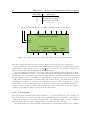
5.1
HDL testing procedure . . . . . . . . . . . . . . . . . . . . . . . . . . . . . . .
53
6.1
Experimental setup . . . . . . . . . . . . . . . . . . . . . . . . . . . . . . . . .
56
7.1
7.2
7.3
Static pattern application result . . . . . . . . . . . . . . . . . . . . . . . . . .
Random pattern application result . . . . . . . . . . . . . . . . . . . . . . . .
Hillclimbing fitness plot . . . . . . . . . . . . . . . . . . . . . . . . . . . . . .
59
60
61
.
.
.
.
.
.
.
.
.
.
.
.
.
.
.
.
.
.
.
.
.
.
.
.
.
v
7.4
7.5
Hillclimbing fitness plot, failing genomes . . . . . . . . . . . . . . . . . . . . .
Hillclimb rerun . . . . . . . . . . . . . . . . . . . . . . . . . . . . . . . . . . .
63
64
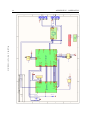
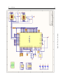
E.1 The toplevel schematics . . . . . . . . . . . . . . . . . . . . . . . . . . . . . .
E.2 The µC schematics . . . . . . . . . . . . . . . . . . . . . . . . . . . . . . . . .
88
89
List of abbreviations
FPMA Field Programmable Matter Array
EPB External Peripheral Bus
EMB Evolution in Materio Board
GA Genetic Algorithm
TC Timer/Counter
GPIO General Purpose IO
PM Power Manager
SMC Static Memory Controller
PBA Peripheral Bus A
SCG Synchronous Clock Generator
USB Universal Serial Bus
MB Material Bay
MUT Material-under-test
PBA Peripheral Bus A
EBI External Bus Interface
vii
Chapter 1
Introduction
Today the theory of evolution is
about as much open to doubt as
the theory that the earth goes
round the sun.
The Selfish Gene
Richard Dawkins
Construction and evaluation of a prototype board for evolutionary exploitation of materials
for computation.
If you were to walk up to a hardware engineer on the street and ask her how she would
create a device capable of producing the sum of two sequences of binary digits, one possible
solution that could emerge quickly would be that of a half-adder, chained together to create
a full-adder. When inquired further, the engineer would perhaps give the implementation of
such a half-adder using logic gates, and if so inclined she could probably tell you how these
logic gates are implemented using transistors, and finally how these transistors are created
using doped silicon.
Each of the levels of abstraction in the above has its own set of units which describe what
the unit can, or cannot do, in terms of human understanding. In light of this, they are actually
more like constraints on the human design process– we have enough detail knowledge about
the operations of these units or materials to predict in very fine detail how the computation
takes place. As such, we are not exploring what the material, e.g. transistors or doped silicon
can do; this we know very well. We are exploring how we can design abstractions on these
materials so as to better utilize them, given the known constraints. If we somehow manage
to create an erroneous design (at least erroneous by our engineering standards), such that we
operate outside the constraints of the given material or abstraction, we do not have a working
device, at least in the traditional engineering sense and must redesign; yet, would it not be
somehow interesting to see where this “error” leads us? Take the simple issue of operating
below threshold in a CMOS transistor– this is an error by design, yet, research has found
that it is in fact possible to exploit the effects of this “error”.
The point we are trying to make here is that we are not so much exploiting and exploring
the known fact that certain forms of matter has potential for doing computations– we are
exploring the potential of the design imposed and applied to the matter. In Evolution in
Materio we do the opposite: we are interested in exploring the matter, the substrate in which
the computation is done on a very low level– not the design we try on the matter.
2
CHAPTER 1. INTRODUCTION
The method we employ are that of a search in the various ways of “configuring” the
material. We shall consider the material as a black box, upon which we apply voltages to
inputs and read the response from outputs– the internal dynamics of the system inside the
black box, however fascinating and interesting, shall not concern us to any great degree.
A configuration in this search is thus some pattern applied to the inputs of the black box,
possibly a sequence of patterns and these patterns make out the state space, which we shall
search using a Genetic Algorithm.
To enable this search, it would be beneficial to have a easy and fast way to try out various
configurations on this “material black box”, and also to explore several kinds of material.
We are not alone in this quest, and there are already several examples of such exploration
platforms; one of the pioneers in evolvable hardware, G. Pask did experiments with developing
“decision making machines” in solutions of metallic ions[Pas]; A. Thompson has done several
experiments in which the black box is an FPGA [Tho96], and recently, Harding and Miller
has explored Liquid Crystal as a potential matter for computation[HM04]. You can read more
about these in chapter 2.
In this project, we seek to create an experimental platform which is (relatively) cheap,
easily extendable and general enough to enable a wide search in various substances and
configuration of these. Specifically, we wish to create a board whose purpose is to enable
us to easily connect to a material bay. We call this board Mecobo. This material bay is in
essence a small cup filled with electrodes, defining the border between our test system and
the “material black box”. We interface this material bay via an FPGA, and correspondingly
interface the FPGA via a microcontroller capable of communicating using the USB protocol.
The report is structured as follows. Chapter 2 gives motivation for this research, and
also attempts to show the current state of this still Basic Science. Chapter 3 provides details
about the full system setup we utilize to run our experiments and 4 gives the details about
the implementation of our prototyping board. Chapter 5 presents the testing and verification
of the board, along with a short section on the performance of the board in terms of how fast
we can output new values on the output pins of the FPGA.
In chapter 6 we put a feather of science in our engineering hats, and go into depths about
the method we employ in our search of the matter, i.e. details about the setup and algorithms
used. The purpose of these experiments is more of a demonstration of the capabilities of
Mecobo, however they also cover the obvious first step in exploring the space of materials.
Chapter 7 presents the results we have obtained from these experiments. Chapter 8 concludes
the project and gives pointers to further research and improvements to the platform.
In the appendices, you will firstly find a detailed user manual for Mecobo in appendix
A. Code used in chapter 6 can be found in appendix B. We have done a fair amount of
testing, and the plans we used for planning and recording these tests is located in appendix
C. Appendix D gives a detailed construction manual for recreating Mecobo. Finally, E shows
two central schematics; the toplevel and the µC connections. The rest of the source code and
schematics for the project can be found online, at "http://anipsyche.net/mecobo/mecobo_
rev2.tgz".
Chapter 2
Background
We are stuck with technology
when what we really want is just
stuff that works.
The Salmon of Doubt
Douglas Adams
Computation: one word; a thousand meanings. Such is often the case with general terms,
yet one must be careful not to generalize too much, lest the word loses meaning. Computations
are done everywhere and at all times. Let us continue what we started in the introduction; the
act of adding two (fairly small, say, single-digit) numbers. To make it a bit more interesting,
let us first focus on how a human would go about performing this task, without the aid
of a digital electric computer. Somewhat undramatically, most humans would immediately
“see” the answer, without blinking twice. At the abstraction layer 1 of human first-grader
mathematics, this is a trivial computation. Four cows and three apples equals seven cowapples.
Looking closer at what actually happened when this computation was done reveals a rather
different (and complex) truth, however.
Let us assume that the two numbers that is to be added is written down on a piece
of paper. Thus, one of the first things that happen in the computation is that the human
eye detects the light emitted from the piece of paper, and converts the energy present in
photons to electro-chemical impulses in neurons. The exited neuron transmits information
through synapses. This information is received in various parts of the brain, predominantly
the cerebral cortex, where it is interpreted resulting in a perception which can further be
processed in the human brain.
In [Tof05], Toffoli goes on at some length in attempting to properly define computation,
and he states a definition that says
(...) any mechanism that can produce a boundless variety of effects out of a substantial
uniformity of means .
Clearly, by this definition, the example above shows a computation, as do the photosynthesis and a Turing machine. And we have not even been very thorough in our explanation,
nor even begun to cover the complexity involved in interpreting the numbers we perceive on
1
Or perhaps the complete opposite of abstraction; since this is in fact a very concrete example of abstract
algebra, in which one uses an operator with certain properties on elements of a group or ring
4
CHAPTER 2. BACKGROUND
the piece of paper, or any of the other processes that takes place in our brain when adding
numbers.
Toffoli goes on to dismiss his definition as too general, so as to give headway to his argument that one has to bring in evolution and feedback-loops to properly define computation;
however fascinating his argument is, we shall not indulge in it any further, but note that for
the purpose of this chapter, the definition above is sufficient. Further, we shall note that the
examples of computation presented in [HMR08], such as crystal growth from nucleation, a
drop of ink dispersing in a glass of water also fit this definition and can reasonably be thought
of as computations.
2.1
Dealing with complexity
Human beings are exceptionally good at organizing, structuring and “making sense of things”,
at least to the degree of which we ourselves are capable of understanding. We perceive
ourselves as masters of complexity, building ever more intricate and miniature devices, hiding
complexity behind walls of abstraction.
What has made this possible is the human mind’s ability to isolate problems into subproblems, tackling them one at a time in a structured, top-down manner. It is thus rather
depressing then to think that even given the human minds excellent capabilities of organizing and constructing, our “complex” machines are still nothing compared to the complexity
generated by natural evolution[MD02].
The “basic building block” of computers is the transistor, in itself an extremely simple
device, which we, with best engineering practices, try to utilize to create more complexity
out of simpler parts. In [McM00], McMullin and Barry discuss how evolution represents
a “grows in complexity”, from less complex to more complex, while all human engineering
experience shows that we work from something more complex to something less complex–
this is how we solve problems. In contrast, McMullin and Barry argue that evolution tends to
tackle problems by exploring and searching for complex solutions as well as simple solutions,
and that by this, we are achieving a growth in complexity. Nature does not discriminate
between “simple” and “complex” in the sense that the human mind does– we prefer simplicity;
nature prefers whatever increases the fertility rate and decreases mortality, and it can become
arbitrarily complex.
Indeed, Wolfram [Wol86] suggests that we should take inspiration from nature, and the
mechanisms that underlie the complexity shown in nature, i.e. evolution to engineer systems
that are too complex for humans to create by hand.
2.2
Intrinsic hardware evolution
Let us first make a distinction between the general technique of evolutionary computation
and the application of this technique to generate machines capable of doing computations.
There are several examples of using evolutionary techniques to develop hardware, and this
approach is called extrinsic hardware evolution. For instance, in [MJV00] uses an evolutionary
algorithm for finding digital circuits capable of basic arithmetic functions. One of the most
famous experiments is done by Adrian Thompson.
2.2. INTRINSIC HARDWARE EVOLUTION
2.2.1
5
Thompson’s experiment
Adrian Thompson’s well-known and much discussed work with intrinsic hardware evolution
on FPGAs[Tho96] can be seen as one of the first experiments in the field of exploiting physical
properties of materials in recent time, even if Thompson himself did not mention this explicitly
in his papers.
Thompson wanted to evolve a circuit capable of discriminating between square waves of
two different frequencies. He used an FPGA, constrained the design to 10x10 reconfigurable
cells and ran a single-elitism GA with a randomly generated population with a fitness based
on integrating the output voltage over the test tone used as input.
The experiment proved successful, and exploring a successful individual showed several
remarkable points; especially the discovery of bistable oscillators “appearing” in the design,
which Thompson speculates “maybe due to parasitic capacitance”. Taking the design out of
the material it had evolved in and implementing the circuit with separate CMOS transistors
lead to a nonfunctional circuit. In other words, the GA had managed to utilize unknown
properties of the material which were outside the constraints placed by humans wishing to
utilize it.
The key point to note here is that if we look at the transistors as yet another material, they
have proved to have properties which evolution has exploited in ways in which an engineer
most likely would not conceive, because she is constrained by the documented and tested
properties of the transistors.
2.2.2
Lindens antenna
In [MLHL] Derek Linden et. al. presents what has been described as a seminal work in which
evolution was employed to create X-band antenna designs to be used on NASA spacecraft,
specifically for the ST-5 research mission in 2005.
Two approaches were used to evolve the antenna; a standard genetic algorithm that did
not allow branching of the antenna. The genetic representation used is a set of real-valued
scalars, one for each coordinate in the “box” that constrains the size of the antenna. The
fitness was essentially a measurement of the gain of the antenna at two frequencies.
The second approach allowed branching. The antenna is represented using a tree, which
is manipulated by a set of commands, essentially becoming a genetic programming approach.
The two most fit antennas were fabricated and tested at NASA Goddard Space Flight
Center, and complied to the requirements put forth for the mission. In June 2006 ST-5 ended
and the results, available on http://nmp.jpl.nasa.gov/st5/, was that it “operated well
within specification”. Thus it represents the first evolved hardware in space, and successful
to boot.
2.2.3
Fault tolerance
One of the more attractive features of nature is its ability to regenerate. In [HH04] Hartmann
and Haddow presents automatically generated digital circuits that show graceful degradation
with increased noise and failure rate in a simulated environment. By
Their genetic representation is that of a netlist that lists each gate along with it’s inputs,
outputs and type of port, e.g. AND, OR, NOR, and also a list of inputs and outputs to the
circuit as a whole. A tournament based genetic algorithm where mutations are applied at the
gate-level is used. Either the complete gate is changed to a random type of gate, or one of
6
CHAPTER 2. BACKGROUND
the inputs to the gate is connected to a random gate output. Fitness is basically measured
as how well the outputs of the evolved circuit matches that of a target function truth table.
The results of the experiments shows that not only is evolution capable of producing 100%
functional circuits, they are also robust in the presence of noise and errors, and as they note
“the circuits illustrate the ability of of evolution to generate novel designs with beneficial
properties, completely unlike the solutions an engineer would come up with”.
2.3
Exploiting materials
Since evolution obviously is capable of producing working hardware designs, but at present
does not rival the capabilities of human designs, the obvious question is why?. [MD02] goes
into some details about this question. Artificial evolution is in essence a simulation of nature.
Increasing the number of variables in the simulation increases the sophistication of the designs,
however they also lead to a very slow evolutionary process and as Downing and Miller writes,
“they are limited by our own knowledge”. As discussed in chapter 1, human understanding
and knowledge is nothing but a constraint on evolution. In nature, the materials available
for constructing complex designs are numerous, and the physics pertaining to the interaction
of these material are computationally tractable on a digital computer designed by humans,
only if we make certain simplifying assumptions [HMR08].
As such, [HMR08] and [MD02] argue for the approach of Evolution In Materio, in which
we attempt to exploit the richness of the physical world, the iterations and phenomena in
particles on micro- nano- and meso-scale which are beyond human understanding, to do
computations.
The first steps in this direction can be found some time ago, in England.
2.3.1
Gordon Pask
Gordon Pask, a member of the British society of cybernetics prominent in the fifties and
sixties published several papers [Pas] in which his goal was to discuss “the circumstances in
which we can say a machine “thinks”, and a mechanical process can correspond to concept
formation”. Pask may or may not have been aware of the fact that in his experiments he was
one of the first to actually utilize a developmental process to hardware design. In his paper,
he goes into some length discussing some of the more philosophical aspects of thinking; the
difference between an external observer and the participant observer and how these capture
the act of thinking most correctly.
Looking a bit beyond the motivation for his work, in [Pas] Pask first describes two experimental assemblies with which he, in essence, intends to simulate a part of the brain. The
first assembly uses a network of known elements, namely thermally sensitive resistors and
amplifiers. This system would, with the appropriate input go into any number of dynamic
equilibria, determined by the symmetries of the connections. In some senses, this resembles a
Random Boolean Network. The problem with this network of common components are that
they should be completely connected; which were at the time almost impossible to achieve.
Pask however does a crucial observation: “it is possible to see that if the various degrees of
freedom used up in specifying the symmetries of a real life plexus were available, the elements
would act like raw material from which any assemblage might be build”. Rather than attempt
to get close to the fully connected machine, Pask sees that “the effect of adding further initial
degrees of freedom to a plexus of parametrically variable elements is achieved, biologically,
2.4. EVOLUTION IN MATERIALS
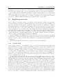
7
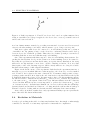
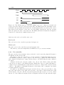
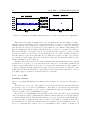
Figure 2.1: Pask’s experiment. S, X and Y are electrodes located on a plane immersed in a
solution of metallic ions. Voltage is applied to the electrodes to create a potential between S
and X, and between S and Y.
in a less clumsy manner, namely by providing raw material of unstructured but structural
elements, the surroundings of an embryo when it starts to grow, being a case in point”.
Pask uses a plane with electrodes connected to it and submerges this into a solution
of metallic ions. By putting voltage on the electrodes, conducting threads would develop
between electrodes of different potential. Thus, there is a definite growth process involved,
something Pask also notices and calls this setup “self building”.
One of his experiments with this setup is to show it’s self-building characteristics. Regarding the threads that develop in the solution as decision-making devices; he wanted to
show that if a problem is found insolvable using one specific thread distribution, the setup
will tend to modify itself into a new device, capable of finding a solution. Now, note that
this is quite a tall order! In many respects, this is exactly what we are doing in evolvable
hardware when trying to build adaptable machines.
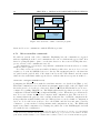
Figure 2.1 shows the essence of the experiment. Pask divides the experiment time into 3
intervals, t2,1 , t3,2 , t4,3 in which different conditions apply to the electrodes, or nodes, marked
as S, X and Y. At t1 , that is, the start of interval t2,1 , X assumes a high positive voltage,
creating a path towards X. At t2 , that is, the end of interval t2,1 , the thread has reached point
P. Pask then changes the voltage of Y to the same as the voltage of X. Given sufficient current,
the thread tended to bifurcate in the interval t3,2 , and if one at t3 returned the parameters
to the same as in t2,1 , the system behaved in a very different manner from the behaviour
observed in that interval; in fact, it was impossible to predict the behaviour in t4,3 based
on observations in t2,1 . As Pask states himself “an observer would say that the assemblage
(system) learned and modified its behaviour, or looking inside the system, that it built up a
structure adapted to dealing with an otherwise insoluble ambiguity, in it’s surroundings”.
As we can see from these results, these early experiments in many respects represents the
start of the field “Evolution in Materials”.
2.4
Evolution in Materials
Several people working in the field of evolutionary hardware have, knowingly or unknowingly
contributed to the field of evolutionary exploitation of materials for computation.
8
CHAPTER 2. BACKGROUND
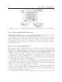
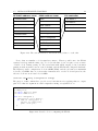
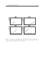
Figure 2.2: Concept of a Field Programmable Matter Array, figure copied from [MD02]
2.4.1
Field programmable matter array
[MD02] envision how they perceive a tool for exploring the richness of materials. One of these
is the Field Programmable Matter Array (FPMA), shown in figure 2.2.
The FPMA is based around the idea that by applying voltages to some material, one
might obtain unexpected physical interactions in the matter under exploration. This if a
rather high-level and not very concrete description of a system for testing the potential of
various materials; but it serves as a general description of most of the systems we describe in
the following sections.
2.4.2
The evolvable motherboard
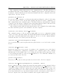
The evolvable motherboard (EM) was conceived “to help build a framework for an FPGA
ideally suited to Intrinsic Hardware Evolution” [Lay98]. It is in essence a switching board
that allows up to 6 daughter-boards to be connected together, each daughter-board having a
number of connections. The EM allows all-to-all-connections between the daughter-boards,
configurable from a host computer, and it also allows for measuring all switch points.
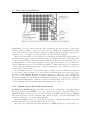
Figure 2.3 shows a simplified representation of the Evolvable motherboard. Observe that
the system allows for up to 6 daughterboards to be connected in a more or less completely
general way. The software library, which is also part of the EM allows the switch arrangement
to be subdivided into a wide array of configuration.
Programming the board is done via a special interface card that utilizes a host PC’s ISA
bus; which in essence is a memory mapped bus. This allows for very fast configuration of the
switches. The down-side with this, of course, is that not many computers ship with ISA slots
anymore, so a more modern approach would be beneficial.
The paper also presents a number of “proof-of-concept” experiments, in which he uses
an array of bipolar transistors as the fundamental building block to evolve NOT-gates. A
generational GA with single-point crossover, rank-based selection and elitism was used, and
three different experiments were carried out.
The first used a population of pre-seeded NOT-gates, and their elite fitness score increased
2.4. EVOLUTION IN MATERIALS
9
Figure 2.3: Evolvable motherboard, from Layzells paper [Lay98]
significantly over about 500 generations. The experiment also showed that evolution had
increased the performance of the pre-seeded gates by utilizing the fundamental law that
resistors in series increases combined resistance, whilst resistors in parallel decreases the
resistance. A good example of evolution simply following the laws of physics.
The second experiment evolved a NOT-gate from scratch, and although a larger number of
generations was required, after about 2000 a vastly better fitness was achieved than any of the
pre-seeded gates managed. Given the result of Thompson [Tho96], unconventional usage of
circuits should not come as a large surprise to anyone who has seen the power of evolutionary
search. This was also the case in Layzells experiment; evolution had chosen to not make use
of the ground-line, but instead made use of the large impedance of the oscilloscope connection
used to monitor the operation.
A point must however be raised with regards to future references on this work. Layzell
does speculate on the fact that “we do not yet know exactly what the most appropriate basic
element for IHE (Intrinsic Hardware Evolution) might be”– which is a correct assessment.
He does not, probably knowingly, look further than human-engineered basic elements and
mentions “transistors; some higher level multi-functional unit; or combinations of different
components including passive resistors or capacitors”. His motherboards, however, proved to
be very useful in later experiments where such questions were explored.
2.4.3
Liquid Crystal Evolvable Motherboard
In [HM04] and [HMR08] Harding and Miller describes the construction of a Liquid Crystal
Evolvable Motherboard (LCEM), a prototype system developed to match the Field Programmable Matter Array (See section 2.4.1) suggested by Miller and Downing in [MD02].
The framework they created is in many ways general enough to test various materials, but
lack the possibility to do so in an efficient manner.
Harding and Miller decided on exploring the properties of Liquid Crystal first, and built
a framework which is general but a fairly narrow prototype.
By using four of Layzells “Evolvable Motherboard”(EM) [Lay98] (see section 2.4.2 con-
10
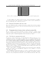
CHAPTER 2. BACKGROUND
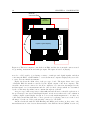
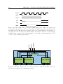
External
connectors
Host
computer
EM
Liquid crystal display
EM
Figure 2.4: The host computer controls the four EMs, and also the 8 external connectors used
for grounding, measurement and analogue input. The figure is based on [Lay98].
nected to a PC capable of producing a variety of analogue and digital signals, and then
connecting the EM to a LCD similar to ones found in most computer displays, they were able
to carry out some initial experiments.
Figure 2.4 shows the main ideas of the prototype board. The figure shows four copies
of Layzells’ EM, the switches controlled by the digital outputs of the host computer. The
external connections are connected to the host computers, one connection was assigned for the
incident signal, one for measurement and the other for fixed voltages which are determined
by the evolutionary algorithm, but is constant throughout each run.
As a prototype, this set-up is more than sufficient and allows for a flexible exploration of
the problem space associated with Liquid Crystal– it is however rather tied to the evaluation
of using a liquid crystal display, though it does not take much imagination to see that one
could easily extend this platform to a more general one by placing connectors on the board,
allowing for break-out on the pads currently connected to the LCD.
Another drawback with the LCD Harding and Miller used is that, as they write, “the
internal structure nor the electric characteristics of the LCD are known”[MD02, Section 3.2].
2.4. EVOLUTION IN MATERIALS
11
This makes it hard to ward against doing physical damage to the display, but it also makes
it harder to actually evaluate the results from the experiments.
Experimental setup and experiments The experiments used a GA with elitism and a
tournament-based selection based on samples of 5 individuals, with 5 mutations per individual.
The genotype was divided in two; with one part specifying the connectivity, that is, how the
switches of the EM is to be configured, and the second part determined the configuration
voltages. The connectivity was specified as a string of 64 integers, and the voltage level was
represented as five 16-bit integers, mapping the 65536 possible values to the range -10 to +10
volts.
Harding and Miller ran a number of experiments. One of them involved evolution of a
non-linear response, with a fitness-test that basically checked if the sampled response values
could be linearly interpolated from previous values. If this was not the case, non-linearity
was achieved.
A second experiment, in which they attempted to evolve a transistor did not come through.
A transistor has low output when input voltage is below a certain threshold, and high otherwise. In their experiments, the threshold was set to 1.5V, and they did not manage to evolve
such a phenotype. There are several unanswered questions with regards to why a suitable
response was not found, since the results indicate that there are a number of times such a
step-wise response is observed.
12
CHAPTER 2. BACKGROUND
Chapter 3
System overview
He that breaks a thing to find
out what it is has left the path
of wisdom.
Gandalf
This chapter will attempt to give an overview of the complete system from an end user
perspective.
Ultimately, the purpose of the system is to be able to apply electric current to a material,
and to somehow read the response, if any, from this material. As such, the simplest incarnation
of the system would be to put two electrodes in a cup of some kind of matter, say water,
apply current from a voltage generator to one of the electrodes and read the other electrode
with a voltmeter, the voltage generator and voltmeter of course having common ground.
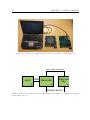
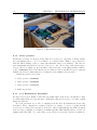
The system we have constructed is nothing more than an elaborate version of this setup,
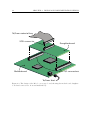
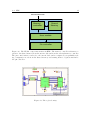
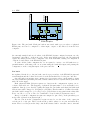
which is pictured in figure 3.1. There are three components pictured.
1. Host computer. The host computer is a standard USB-capable computer, preferably
running some version of the Linux operating system.
2. Mecobo. MEA Connector Board.
3. Material bay.
Schematically, the complete system is shown in figure 3.2.
The host computer communicates with Mecobo using Universal Serial Bus (USB), sending commands which are interpreted and executed by the controlling unit on Mecobo. For
example, the host can issue the command setPattern(pattern) which, causes the output
electrodes of the MB to take on the pattern supplied as argument.
3.1
Host computer
The host computer is any computer capable of running linux, and having an USB-connector.
To utilize Mecobo, the host computer has a dynamic library installed, libEMB, which we
have created. This library acts as the front-end to the complete system and provides a set of
functions to set and read the electrodes of the MB, along with various utility functions.
14
CHAPTER 3. SYSTEM OVERVIEW
Figure 3.1: 1. The host computer with a USB cable 2. Mecobo 3. Material bay.
Set electrodes
USB Meacobo
Host
1
2
Material
bay
3
Read values
Figure 3.2: The host computer controls the material bay through Mecobo, which is the system
created in the project.
3.2. MB
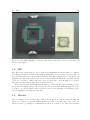
15
Figure 3.3: The MEA Amplifier to the left, without the replaceable electrode array inserted,
shown on the right.
3.2
MB
The MB is an off-the-shelf product bought from multichannel systems [mul], a company
specializing in high-performance measuring instruments for electrophysiology; the study of
how electricity affects biological cells and tissues. The MB consists of two components, an
amplifier base unit, and a replaceable electrode array, which essentially is a cup with several
electrodes. A picture of this replaceable electrode array can be seen in figure 3.3, together
with the base unit without this electrode array inserted.
Notice the holes surrounding the pins in figure 3.3. These are the custom stimuli ports we
use to read and apply voltage, and correspond to the port labeled “stimulus input” in figure
3.4. We do not use the SCSI-connector present on the board currently, consequently nor the
per-pin amplifiers present in the base unit.
3.3
Mecobo
Mecobo, number 2 in 3.1 is the “glue” that connects the host computer with the MB. In
essence, it consists of a µC and an FPGA. The µC is the controlling unit of the board. It
sits in a busy loop, waiting for commands from the host computer, decoding and executing
16
CHAPTER 3. SYSTEM OVERVIEW
Figure 3.4: Schematic view of a MEA electrode[mea, p. 13, s. 5.4]
// First create a pin - configuration .
pinconfig_t * config = init_config (64) ; // init to 64 pins
for ( i = 0; i < 64; i ++) {
// Set every other pin to output , default is input .
if ( i % 2 == 0) {
set_pin_mode (i , PIN_OUT , config ) ;
}
}
// generate a random pattern
pattern_t * pattern = g en e ra t e_ r an do m _p a tt er n (4) ;
pattern_t * ret ;
setPattern ( pattern , config ) ;
ret = readPattern ( config ) ;
Figure 3.5: Example of using libEMB
them by further instructing the FPGA via a shared memory area located on the FPGA. This
shared memory area is mapped into the µC address room.
The microcontroller also handles USB, and further debug capabilities such as USART.
Mecobo is composed of a main board and a daughter board. The daughter board connects
to the main board through two 50-pin JAE connectors The microcontroller and the FPGA
communicates via memory mapped I/O, which has come to be a fairly standard way of
mapping and interfacing external peripherals because of it’s simplicity.
3.4
A complete example
We will now take the time to explain and work through a complete example of using Mecobo
and libEMB.
The code snippet in figure 3.5 demonstrates the usage of libEMB. We first create a pinconfiguration, which is passed around during the usage of the various libEMB functions. We
set every other pin to output, and proceed to generate a pattern of 4 bytes.
When calling setPattern() with these two arguments, a subroutine in setPattern()
merges the configuration and the pattern to a complete pinbank configuration string that is
then sent to the Evolution in Materio Board (EMB) in an evoframe using the USB connection.
Once these data arrive on the EMB, and in particular, on the µC , the dispatcher on the µC
checks the header of the evoframe, sees that it is a command to write pin configuration data
to the FPGA, and proceeds to write the data found in the payload of the evoframe to the
3.4. A COMPLETE EXAMPLE
17
shared memory on the FPGA. To complete the command, the µC writes the command register
address of the shared memory with the appropriate command, in this case CMD WRITECFG. The
µC will then idle, waiting for the FPGA and respond with a OK-message once the command
is completed successfully.
When setPattern completes, the call to readPattern follows the same route, of course
exchanging the commands where appropriate. What is returned from the EMB is all the
pin values read from the FPGA I/O-pins, even the ones used as output. A subroutine
in readPattern masks out the pins defined as output in the configuration, and returns a
pattern t whose data is only the values read from the FPGA I/O-pins defined as input.
18
CHAPTER 3. SYSTEM OVERVIEW
Chapter 4
Design and implementation details
Talk is cheap. Show me the
code.
Linus Torvalds
This chapter provides a look at the design and implementation details of Mecobo and
accompanying software. The difference between the two terms design and implementation
is sometimes hard to define. Common engineering methodology often dictates a hierarchical
decomposition of the problem, and one can argue that there is indeed both a design, i.e.
which entities are present at this level and where they are connected, and an implementation,
i.e. how these entities work and possibly communicate.1
In this report, when we specify design we will refer in particular to which types of entities
(e.g. a µC , a FPGA) are present on Mocobo, and where and by what means these entities
are connected. This hierarchical level however does not entail looking into each of the entity
black-boxes, and as such does not for instance take into account exactly what kind of FPGA
is used.
The production of the board and software represents the largest part of this project,
motivating an in-depth study of the details. We will first present the complete system pieceby-piece, holding off any discussions pertaining to the various choices until section 4.9.
Note that we did two iterations of the board construction; which we call version 1 and
version 2. If clarification is needed, we will explicitly state what version we are discussing. If
no version is mentioned, the discussion is relevant to both version of the card.
One last thing worth mentioning before we start is that even if this chapter is called
implementation details, the only way to see all the details is to study the source code and
the gerber files for the PCB. Reading this chapter however, should make these things more
comprehensible.
4.1
System parts
Before we start describing how all the parts of the experimental system fits together, we take
a few steps back to do a quick overview of how we break down this chapter, and where we
1
Often, a useful way of separating the two is this: if one perceives the entity as a black box, and it can be
replaced easily with another black box operating in the same manner as the first one, it is part of the design.
If one discusses the black box in particular, it is part of the implementation.
20
CHAPTER 4. DESIGN AND IMPLEMENTATION DETAILS
EMB board
Host
Material
Bay
USB
Microcontroller
Daughter
board
RS232
FPGA
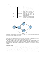
Figure 4.1: Overview of Mecobo. The host computer sends commands to the microcontroller
via the USB interface. The command is understood by the microcontroller which utilizes the
FPGA to apply current to the material bays’ electrodes. Note the separation of the FPGA
to the material bay through a daughter board, allowing for a flexible way of extending the
board with additional features such as analogue in-out and output.
consider each part to fit in.
1. Hardware: Component selection, schematic drawing, soldering and hardware debugging–
all that is required to construct a physical PCB. We start off with this in section 4.3.
2. HDL coding: Designing the hardware components for the FPGA, found in section 4.4.
3. µC setup: Selecting, activating and programming peripherals such as clock managers,
interrupt controllers and static memory controllers. Details in section 4.5.
4. libEMB: A software library meant to ease usage of Mecobo from the host computer.
This is divided in two parts. The dynamic library located on the host computer is
described in section 4.6. The “brother” of the host library that runs on the µC is found
in section 4.7
5. Documentation: A detailed users manual for the complete system. The manual can be
found in the appendices, section A.
4.2
Design
We start off by going one step down in the hierarchical break-down respective to chapter 3,
looking at the design of Mecobo.
Figure 4.1 shows the main ideas of how our prototype board is designed. [HM03] was a
significant inspiration for this. The figure shows the host, connected to the micro-controller
through an USB connection. Also shown is the RS232 connection. The microcontroller is
further connected to FPGA through a 16-bit wide databus with a 23-bit wide address bus, of
which only 12 is currently in use. 100 of the remaining I/O-pins are connected to two 50-pin
pin headers on version 1, changed to two 50-pin JAE PC-board stacking connectors in version
2.
4.3. HARDWARE IMPLEMENTATION
21
To/From Mocobo
Material bay
Figure 4.2: The design of the adaptor card plugging into the stimuli-inputs of the material
bay.
Figure 4.3 shows the design schematically. Connecting to the two connectors is a daughterboard, with a 68-pin SCSI-connector, which connects further through a SCSI-cable to our
material-bay adaptor card, shown schematically in figure 4.2.
The adaptor-card was constructed as a convenient way of connecting external stimulus
channels to the material bay, since the SCSI-connector on the board does not allow application
of stimuli to the Material-under-test (MUT).
The communication between the microcontroller and the FPGA is done via a shared
memory that is mapped into the microcontrollers memory region.
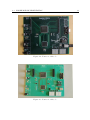
A picture of the first version of Mecobo can be found in figure 4.4.
A picture of the second version can be found in figure 4.5.
4.3
Hardware implementation
The largest components in the system are the FPGA and the µC . In the following we will
give details about these, and also briefly mention the other components found on the board.
FPGA
To fully utilize the material bay, we first and foremost needed a way to connect a large number
of I/O-pins to a SCSI-connector, and to provide a convenient way to control these pins. The
22
CHAPTER 4. DESIGN AND IMPLEMENTATION DETAILS
To/From material bay
SCSI connector
Daughterboard
I/O-connectors
Motherboard
To/From Host
Figure 4.3: The design of the Mecobo prototype board, showing the motherboard, daughterboard and connectors to host and material bay.
4.3. HARDWARE IMPLEMENTATION
Figure 4.4: Version 1 of Mecobo.
Figure 4.5: Version 2 of Mecobo.
23
24
CHAPTER 4. DESIGN AND IMPLEMENTATION DETAILS
solution was obvious; use an FPGA.
The choice of FPGA, the Spartan 3E [Xil09], was based on the fact that it is cheap, easily
available and comes in a package (PQ208) that provides a fair number of I/O-pins and is
possible to solder by hand (0.5 mm pitch).
The PQ208-package has 158 I/O-pins, of which 32 are input-only[Xil09]. This is actually
a bit low, we would have liked to see at least 200 pure I/O-pins, but time-wise and cost-wise
we simply could not afford to use packages based on ball-grid-arrays (BGAs). We do not have
the equipment to solder these ourselves, so shipping them off to be soldered would be costly
and take a lot of time. Finally, BGAs often suffer from bad connections due to solder-errors.
The Spartan 3E includes Block-RAM and 158 bonded I/O-buffers associated with I/O
pins, meaning that we can utilize tristate-buffers on all the I/O-pins. This was a crucial
requirement, as we sometimes want to disconnect the pins from the MB.
The microcontroller
The microcontroller plays a very central part in the design of Mecobo.
As a “bare-bones”-solution to interface the FPGA we could have implemented a RS-232controller or similar on the FPGA. However, RS-232 is slow and old– recent computers simply
do not ship with a serial port at all. We wanted to use USB for communicating with the
prototype board, in fact, it was a requirement for the end product. Implementing a USBcontroller in FPGA is possible, but would take a large amount of time. Using a microcontroller
with a built-in USB-controller freed us from this problem.
First and foremost, it had to be hand solderable with a small rate of solder errors. In
practice this means a pitch of minimum 0.5 mm.
Another requirement was to make it possible to quickly re-program the FPGA from the
host computer, and storing the configuration on the microcontroller. Thus, we required onchip flash, with a minimum size of 277 KB, the size of the XC3S500E configuration file.
Taking these factors into account, we decided on an Atmel AT32UC3A0512– a tried and
tested (at our department) 32-bit microcontroller with 512KB of on-chip flash, 64KB of onchip SRAM and a USB peripheral controller.
MAX232
Because the drive strength of the µC is 3.3V, and the RS232-standard dictates 5.0V logic
levels, the need a +5V driver circuit. The MAX232[IC] has been used in various other
projects at our department and has proven to be a reliable and simple chip.
Other components
The rest of the components are two 15-segment LEDs, two DSUB-9 connectors, one USB
type B connector and for the second version of the board we also used two JAE 50-pin
Board-to-Board connectors.
4.3.1
PCB
We have included the gerber files for both the versions in the appendices.
4.3. HARDWARE IMPLEMENTATION
25
Signal routing
The routing was mostly done by hand, since the auto-routing tools of our chosen PCB design
software did not function properly at the time. We later got this working, but by then we
had routed the major parts by hand anyway.
Calculating trace widths is not an exact science, or it is, but the exact science involves
setting up a large set of differential equations per trace. There are however several tools
available that create approximate solutions. One of them can be found online at [pcb]. Since
we configure the I/O-pins of the FPGA to maximally drive 16 mA, and we have a trace
thickness of 0.5 mm dictated by the PCB-stack chosen, the tool reports a required trace
width of 0.00018 mm. Thus, when we choose to use a trace width of 0.254 mm, which is a
vast over-estimate, the reason is more one of cost. Smaller trace widths means higher copper
costs.
Calculating the required via-sizes is a bit more tricky. In [BG] Brooks and Grave present
a short argument for doing a back-of-napkin estimate of via sizes: given that one has tuned
the trace width to the minimum, the diameter of the via needs to be approximately a third
of the trace width connected to the via, given a few assumptions such as that the thickness
of the via walls are the same as the trace height:
d=
w
−t
π
(4.1)
where d is the diameter of the via, w is trace width and t is the assumed equal trace and trace
thickness. Furthermore, since t << w, we further simply and arrive at the above-mentioned
estimate; d ≈ w/3.
We have chosen two kinds of vias, since having a large number of different holes increases
the cost because of tool change during production. Vias used for IO traces, which are 0.254
mm in diameter, and vias used for power traces are usually around 0.512 to 1 mm in diameter.
Comparing with the estimate of via sizes mentioned above, we are again vastly overestimating, and the reason is again one of cost.
Powering the board
The power budget is based on quiescent measurements provided by the manufacturers of the
chips used. Xilinx reports a current requirement for the XC3S500E of 25, 0.8 and 18 mA for
the core, I/O and aux supplies respectively [Xil09, page 121, table 79].
Atmel reports a power consumption of typically 20 mA when the CPU is running at 36
MHz, which is below our clock rate of 16 MHz [Atm09, page 768, table 38-9]. Furthermore, we
use the general purpose IO controller, interrupt controller, timer controller, power manager,
USB, external peripheral bus and static memory controller, summing up to 184 µA.
The last chip that could potentially draw a fair amount of power is the MAX232, used
for driving the UART to sufficiently high voltage levels. The data sheet [IC, table 1], reports
a typical power consumption during transmission of 5 µA, or a maximum of 40 µA.
Summing up these figures gives us a rough power estimate of about 65 mA, and we
conclude that we can power the board with any PSU capable of providing at least this. For
our project, we use a 220V converter that provides 180 mA, which has not given any problems
as far as we can tell, with regards to power stability.
26
CHAPTER 4. DESIGN AND IMPLEMENTATION DETAILS
Routing the power
The power layer is divided in 4, one division for 1.2V, 2.5V, 3.3V and 5.0V. The two first are
required for the FPGA, while 3.3V is used by the microcontroller and is also the voltage used
for I/O, dictating an I/O-standard of LCMOS33[jes].
Each voltage level is regulated with LM317 adjustable voltage regulators, connected to
one electrolytic capacitor to provide power smoothing. There is also one 0.1uF capacitor for
each pair of IO-pins, and at least one capacitor associated with each power pin on the FPGA
and microcontroller, at times more.
The core voltage of the microcontroller is 1.8V. It however has internal voltage regulators
to create the required voltage from 3.3V input pins, given sufficient charge pumps (capacitors).
4.3.2
Version 2
A picture of version 2 of Mecobo can be seen in figure 4.5. There are no large visible changes
compared to version 1, save for the new board-to-board connectors that are easier to work
with than standard pin-headers since they tend to require large amounts of force to connect
and disconnect. Internally, the power layer has been laid out a-new so as to move the power
layer dividers further away from drill holes, which was a problem on v1 where we would get
a short circuit if a certain part of one of the pin headers was connected. There are also a
number of smaller bug fixes that we found in version 1.
4.4
HDL
Figure 4.6 presents an overview of the hardware design running on the FPGA. There are four
main components; the shared memory, the memory controller, the user module and the pin
controller.
4.4.1
Toplevel
The toplevel entity, whose ports can be seen in figure 4.7, is the topmost level in the FPGA
design hierarchy and is responsible for connecting the shared memory controller, memory, pin
controller and user module together in the manner shown in figure 4.6.
This is also the level that is associated with the physical mapping of the FPGA I/O-pins,
and the internal logic. As such, it represents the last “logic” border before current actually
passes out to the board connectors, through the daughterboard and into the material under
test in the material bay.
4.4.2
Memory controller and shared memory
The memory controller provides the interfaces used to acces the memory shared between the
user module and the µC . Figure 4.8 shows the two interfaces; one external and one internal.
The external interface is connected to the external (hence the name) µC through a 16 bit
in-out databus, a 23 bit address bus along with read, write, chip select and wait control signals.
The internal interface is connected to the internal (relative to the FPGA) user module. By
issuing requests to these two interfaces, the user module and the µC can access the same
memory.
4.4. HDL
27
Microcontroller
Memory
controller
Shared
Memory
User module
Pin controller
Figure 4.6: The FPGA components written in HDL. The memory controller arbitrates requests to the shared memory from the user module and from the external memory controller.
The pin-control unit is connected to the user module, and is configured by sequentially reading configuration words from the shared memory and writing them to registers internal to
the pin controller.
1
U_PSU_JACK
PSU_JACK
2
3
4
3V3
GND
U_EIMA_PSU
EIMA_PSU
PI 102 PI 104 PI 106 PI 108 PI 10
COFPGAOSC
OSC
FPGA
2
PIFPGA OSC01 1
GND
COP1
P1
Header 5X2
GND
ENBL
1
3
5
7
9
2
4
6
8
10
A
PIFPGA OSC04
4
3
A
PIFPGA OSC02
OUT
PIFPGA OSC03
Vcc
3V3
oscil
UC_TCK
UC_TDO
UC_TDI
UC_TMS
PI 10 PI 103 PI 105 PI 107 PI 109
avr.SchDoc
R2OUT
R1OUT
T2OUT
T1OUT
PIUC0SERIAL04
GND
788753-1
T2IN
T1IN
R2IN
R1IN
NCS3
fpga.SchDoc
M0
M1
M2
11
PIUC0SERIAL011
TCK
TDO
TDI
TMS
NCS2
PIUC0SERIAL03
PIUC0SERIAL08
HWSAP
NWAIT
DATA[0..15]
ADDR[0..23]
HSWAP
BUSY
DATA[0..15]
ADDR[0..23]
DATA[0..15]
ADDR[0..23]
CCLK
SERIAL_OUT
USART-RXD
USART-TXD
COFPGA0SERIAL
FPGA_SERIAL
NRD
1
RE
WE
CE
AT32UC3A NWE/NWR0
NCS1
PIFPGA0SERIAL01
6
PIFPGA0SERIAL06
2
7
3V3
COINT0BPU
CCLK
DIN
B
PI N T0B PU01
PI N T0B PU02
4.7k
7
3
8
4
9
PIUC0SERIAL09
5
PIUC0SERIAL05
PIUC0SERIAL07
INIT_B_PU
U_MAX3232
MAX3232
PIUC0SERIAL06
2
PIUC0SERIAL02
M0
M1
M2
1
6
PIUC0SERIAL01
10
PIUC0SERIAL010
B
CLOCK
COUC0SERIAL
UC_SERIAL
Spartan 3E
INIT_B
PIFPGA0SERIAL02
RESET
PIFPGA0SERIAL07
3
PIFPGA0SERIAL03
COP2
P2
PIFPGA0SERIAL05
5
GND
NCS0
NBS1/NWR1
788753-1
6
5
4
3
2
1
PIP206
PIP205
PIP204
PIP203
FPGA_TDI
TDI
FPGA_TMS
TMS
FPGA_TCK
TCK
FPGA_TDO
TDO
PIP202
PIP201
PROG_B
2V5
CODNE0PU COPRG0BU
DONE
Header 6
GND
C
PIDONE0PU01
PI ROG0B PU01
PIDONE0PU02
PI ROG0B PU02
4.7k
C
PROG_B
DONE
INIT_B
DONE_PU
PIFPGA0SERIAL04
9
PIFPGA0SERIAL09
330
PROG_B_PU
8
4
PIFPGA0SERIAL08
USB D+
USB DUSB_VBUS
11
PIFPGA0SERIAL011
RS232_TX
RS232_RX
10
PIFPGA0SERIAL010
2V5
PIJ104 PIJ103 PIJ102 PIJ101
GND
D+
DVBUS
4
3
2
1
GND
J1
COJ1
1470156-2
PIJ106 PIJ105
Title
D
Size
D
Number
Revision
A4
Date:
File:
1
2
7/28/2010
F:\master\mocobo\eima_toplevel.SchDoc
3
Figure 4.7: The toplevel entity
Sheet of
Drawn By:
4
28
CHAPTER 4. DESIGN AND IMPLEMENTATION DETAILS
Databus
Address
Read Write Select Wait
External signals
Data in
Memory Data out
signals
Address
Write
Clock
Reset
Internal signals
Data in Data out Address Read Write Select Wait
Figure 4.8: The shared memory controller.
Because the memory we create is a single-port memory, both entities cannot access the
memory at the same time. This entails some way of delaying a request from one of the entites
while the memory controller finishes with the other. A common way of handling such delay
with standard SRAM chips is to implement a wait signal on the chip that is deasserted once
the memory is available on the SRAM data port. This is the same approach we follow.
The external and internal entities have an “wait” input signal, which the memory controller can assert. If this signal is asserted, it is the responsibility of the entitiy monitoring
this flag to freeze its operation, but keep both the control and data on the buses until the
memory controller deasserts this signal, indicating that it is finished serving the request. In
pseudocode:
while (1) {
if e x ternal_chip_select {
a s s e r t _ i n t e r n a l _ w a i t _ s i g n a l () ;
h a n d le _e x te r na l_ r eq u es t () ;
d e a s s e r t _ i n t e r n a l _ w a i t _ s i g n a l () ;
while ( external_chip_select ) { sleep () ; }
}
if i n ternal_chip_select {
a s s e r t _ e x t e r n a l _ w a i t _ s i g n a l () ;
h a n d le _i n te r na l_ r eq u es t () ;
d e a s s e r t _ e x t e r n a l _ w a i t _ s i g n a l () ;
while ( internal_chip_select ) { sleep () ; }
}
}
To the two connected entities, the memory controller appears to be any standard SRAM
chip with a busy-wait control line.
The FPGA does not have internal SRAM, but it does have several banks of DRAM,
collectivly known as Block RAM. We utilize this as the shared memory. As such, one can
think of the memory controller as a translator between static memory requests and dynamic
memory requests.
To access the shared memory, a common SRAM protocol must be followed. We present
4.4. HDL
29
Clock
Addr
Data
CS
RE
Wait
Figure 4.9: The FPGA memory controller’s (FMC) read cycle. When an external read
request lowers the chip-select and read-enable lines, the FMC asserts the wait-signal on the
next flank. As long as this assert is held, the external unit should freeze, but keep the control
lines asserted and addresss on bus. As soon as the FMC deasserts the wait, the external
unit can capture the data on the data bus. The FMC will then hold until the CS-signal is
deasserted to acknowledge a finished memory read.
this next as the read cycle and the write cycle.
Read cycle
The read cycle for the controller is presented in figure 4.9.
Write cycle
The write cycle for the controller is presented in figure 4.10.
The memory controller is implemented in HDL as a two-process state machine.
4.4.3
Pin controller
The pin controller, shown in figure 4.11 provides the border between the physical I/O-pins of
the FPGA, and the user module.
The purpose of the pin controller is to provide a means to dynamically change the mode
of the FPGA I/O-pins (i.e. input, output or disconnected), to sample the MUT using the
pins configured as input and to apply current/voltage to the MUT using the pins configured
as output.
As figure 4.11 the pin controller consists of 1 to B pin banks. Each of these pin banks
controls a proper subset of the FPGA I/O-pins. Which pins connect to which bank must be
configured before synthesizing the design and is not subject to change in the current versions
of Mecobo. The number of pinbanks is a function of the width of the “configdata” bus, which
we shall explain in a moment.
In addition to the FPGA I/O-pins, figure 4.11 also shows 3 other ports; pin values, config
data and bank address, along with read and write control lines. When writing the bank
address input to the pin controller, the address passes through a log2 n-to-1 decoder, which
asserts one of the banks select-inputs. If the read-signal is asserted, the pin bank will output
30
CHAPTER 4. DESIGN AND IMPLEMENTATION DETAILS
Clock
Addr
Data
CS
WE
Wait
Bank address
Configdata
Pin values
Figure 4.10: The FPGA memory controller’s (FMC) write cycle. When an external read
request lowers the chip-select and read-enable lines, the FMC asserts the wait-signal on the
next flank. By lowering chip-select and write-enable, the external unit also is responsible for
asserting data- and address-busses until the FMC’s wait-signal is deasserted, acknowledging
a finished write operation. Note that the number of cycles the external unit needs to hold
could be longer than this figure indicates.
Bank select
...
Pin bank
Pin bank
...
...
...
Pin bank
...
Figure 4.11: The pin controller decodes a bank address into a bank-select signal so that only
the addressed bank gets it’s configuration updated.
31
Select
Data
Pinvalues
4.4. HDL
Config register
...
D
D
D
D
D
D
...
FPGA I/O-pins
Figure 4.12: The pin bank. Each pin bank is associated with a proper subset of physical
FPGA pins, and can be configured to either input, output or disconnected, from the host
computer.
the currently sampled and stored values of the FPGA I/O-pins configured as input onto the
bus named “pin values” on the next cycle. If the write-signal is asserted, the pin bank will
capture the values present on the “configdata” bus on the next flank, causing a reconfiguration
of the mode and values of the FPGA I/O-pins.
To write all the bank configurations, one is required to iterate over all banks in a sequential manner, addressing each one at a time using the bank addr input, and putting the
configuration on the configdata input of the pin-controller.
Pin bank
As explained briefly above, the pin bank controls a proper subset of the FPGA I/O-pins and
as such implements the behaviour described at the hierarchical level of the pin controller.
One pin bank, seen in figure 4.12 contains 1 2×i-bit register, where i is the number of pins
associated with that particular pin bank, i tristatebuffers, and 2 × i synchronizers, symbolized
with “D” in the figure.
Each physical FPGA I/O-pin requires two bits from the configuration register, in accordance with table 4.1. The mapping of physical I/O-pins must be done statically before
synthesis. Pins (1, n) are divided equally amoungst the pin banks, such that pin bank with
address 0x00 will be mapped to I/O-pins (1, n/B) where B is the number of banks. Generally,
pin bank i will be mapped to (i × n/B, (i + 1) × n/B). If there is any pins left after this, that
is if n mod B = r, r 6= 0, a “left-over” bank will be created with r I/O-pins associated.
Bits (i, i+1) in the configuration register are assigned to pin i. Bit j on the pin values-port
is the value captured from physical pin j.
The two bits from the configuration register is used to set the value of the ouput pin
and the mode of the pin. Table 4.1 shows the possible values for one pin, and what they
mean. The second bit (from the left) controls the tristate buffer– 1 means connect, 0 means
32
CHAPTER 4. DESIGN AND IMPLEMENTATION DETAILS
Pin values
00
10
01
11
Pin mode
Output pin, pin low
Output pin, pin high
Input pin (output Z)
Not used
Table 4.1: Interpretation of per-pin configuration bits in bin banks
Data out Data in Address Read Write Select Wait
Shared memory interface
Clock
Reset
Pin controller interface
Read Write
Bank
Bank
Bank
pinvalues configdata address
Figure 4.13: The user module entity. The intial state is “Read Command”.
disconnect; while the first bit is used as the output value if the pin is an output pin.
One peculiarity worth restating is that if an I/O-pin is designated as output pin, the value
output will be captured and put onto the pin value bus. It is the responsibility of the host to
filter out these values when sampling the FPGA I/O-pins.
The two D-flip-flops that sit between the bank output and the physical I/O-pin in figure
4.12 are synchronizers, added to avoid metastability in the FPGA, something we believe
we experienced several times before implementing this fix; basically the FPGA starts acting
weirdly. This is, however, somewhat of a limiting factor with regards to the open-endedness
of the search; metastability is an interesting phenomena in it’s own right and there is a
possibility for evolution to exploit it in some unforseen way. Alas, we must also consider
functionality of our experimental setup. Combined together, these synchronizers make up a
complete register for the pin values, and as such there is no need to add yet another register
explicity for storing the sampled values from the input pins.
4.4.4
User module
The user module, shown in figure 4.13 is meant to be easily replacable by other designs, we
have however tried to create a general version that illustrates the capabilities. The purpose
of the user module is to act as an executing unit of the FPGA design, reading commands
from the shared memory and realizing them by accessing the pin controller.
It is implemented as a state machine reading memory address 0xA, which is the command
4.4. HDL
33
Numeric value
0x0
Command
Noop
0x1
Configure pins
0x2
Read Pins
0x3
Status
Description
The module idles, all state is
left unchanged, including pin
configuration.
Reads configuration data
from shared memory, and
writes it to the pin banks.
Reads all pin values and
writes the result back to the
shared memory.
Writes various status and diagnostic data to shared mem.
Table 4.2: Table of commands understood by the FPGA user module.
Read
config
Read
command
Clear
command
Dispatch
Write
pin values
Figure 4.14: The user module statemachine. Note that each of these states can take several
cycles, and generally consist of sub-states.
register. The state machine dispatches based on the values found at this memory location.
The commands that the user module recognizes are listed in table 4.2.
The state machine for the user module is presented in figure 4.14. The module first reads
the command register, dispatching on the read command. After the command is complete,
the state machine will clear the command register to acknowledge a successfully completed
command.
Setting pin values
Setting the pin values entails both setting the mode of the pins and setting which value, that
is, high or low, that should be put on the pin. When the command register is written with
the value corresponding to configure pins (0x1), the user module will enter a loop in which it
sequentially fetches a predefined number of words from the shared memory.
For each fetched word it will select the corresponding bank, starting at bank 0, asserting
34
CHAPTER 4. DESIGN AND IMPLEMENTATION DETAILS
the pin controller write signal and applying the fetched word on the data lines of the pin
controller.
Since the pin controller and the user module are both located on the FPGA it is easy to
time pin controller reads and writes, and no acknowledgement or such is needed.
Reading pin values
Reading back data happens in a similar fashion, except writing the shared memory is replaced
by reading from that memory location.
The user module will sequentially address each bank, starting at 0, assert the read signal
and one cycle later the data will be ready on the pin controllers output ports, ready to fetch
and further forward to the shared memory.
4.5
Microcontroller
The µC is the controlling unit of Mocobo. Its responsibilties are to provide an user-interface
to the board, to configure and utilize the FPGA and to provide feedback to the end-user
about the status of the computations. Because we chose a fairly powerfull µC , it is also
possible to run a Genetic Algorithm (GA) on it, if one is so inclined.
The peripherals of the µC are easy to work with because most of them have drivers
provided by Atmel. Since the framework was written in C, we opted to write most of our
software in the same language. It would of course be possible to intermingle this with C++
or compile the framework to a dynamic library and hook into it using some other language.
4.5.1
The Atmel driver framework
This framework provides drivers for all the peripherals. Unless one particular peripheral
depends on another (such as the USART depending on the interrupt controller) one can
include only a subset of the complete framework in the code. All the drivers operate in much
the same manner; with one function initializing and setting up that particular peripheral. If
the peripheral does depend on other peripherals, these must also be initialized in advance. In
general one only needs to include the header file corresponding to the peripheal one wishes
to use, i.e. pm.h for the power manager, and link against the framework while building. This
header file usually contains one or more intializing functions and various functions for using
the peripheral.
The framework also includes several example applications and utilities which provide some
convenience functions. For instance, we use the debug-utility, which only requires the setup
of a USART connection to access a set of functions for formatting debug output.
In our code, all the initialization of the hardware happens in the function setup hw(),
called once from the main() function.
4.5.2
Peripheral setup
We will now go through each of the driver-initalization routines used.
4.5. MICROCONTROLLER
35
Power Manager
The power managers[Atm09, p. 53] responsibilities include controlling the clocking infrastructure, which is what we use it for.
We setup 3 different clock domains; the CPU clock, Peripheral Bus A (PBA) and the USB
clock. The CPU clock and the PBA clock is setup to 16MHz and 4MHz respectively, by setting
the fields of a pm freq param t-struct, and passing this to pm configure clocks(). The USB
clock is setup to the required 40MHz by a separate utility function, pm initialize usb clock().
General Purpose IO (GPIO)
The GPIO-controller[Atm09, p. 170] provides means for multiplexing of up to four peripheral
functions per I/O-line. It does more, but this is mainly what we use it for. There is no
initialization required for the GPIO module. To use it, one simply creates a gpio map t
which maps physical pins to peripherals. This structure is the passed to gpio enable module.
The drivers takes care of calling this function, but one has to do the job of selecting which
peripheral is to be used at which physical pin.
Interrupt controller
The interrupt controller is responsible for informing the CPU of any peripheral activity which
creates interrupts. To initize this peripheral, we first turn off exception handling, set the base
for the interrupt autovector as explained in [Atm09, p. 99], and call INTC init interrupts().
The interrupt controller driver supports registering which functions to call upon which
interrupts. This is done with INTC register interrupt(), and we will further mention this
when we use this function later.
USB controller
The USB-controller [Atm09, p. 497] first needs to negotiate a connection with the host
computer. This is known as enumeration in USB lingo[Gro], and is achieved by the function
usb device task init(). During enumeration, the device, in our case the µC will identify
itself to the host, in our case the host computer, by presenting information such as maker
ID and other metadata. In this process, the class of the USB connection is also negotiated.
We identify the µC as a CDC device, which provides a simple general-purpose connection
type.[Gro].
We furthermore identify the connection as a simple USB ACM modem device[Pav99],
causing the Linux kernel to associate a standard character-oriented ACM modem driver with
the created device node, making it exceptionally easy to send and receive data on the host
computer.
Further setup happens by first initalizing the dedicated USB peripheral clock in the
power manager, as explained in section 4.5.2. We then initalize the USB driver by calling usb init device() which takes care of setting up the endpoints, which are USB termination points used to send and receive data, and are basically FIFOs. The framework
provides macros to read and write to and from USB endpoints, Usb read endpoint data()
and Usb write endpoint data(), which is callable once these endpoints have been setup.
We use these macros in our datalink abstraction layer.
36
CHAPTER 4. DESIGN AND IMPLEMENTATION DETAILS
Value
NRD SETUP
NRD PULSE
NRD HOLD
NCS RD SETUP
NCS RD PULSE
NCS RD HOLD
NWR SETUP
NWR PULSE
NWR HOLD
NCS WR SETUP
NCS WR PULSE
NCS WR HOLD
FPGA cycles
1
4
1
1
4
1
1
4
1
1
4
1
Table 4.3: The µC SMC timing numbers, in FPGA cycles. Please refer to [Atm09, p. 374,
375] for details.
External Peripheral Bus and Static Memory Controller
The External Peripheral Bus (EPB) [Atm09, p. 145] is a general way to interface external
peripherals, and has an internal static memory controller (SMC) which can be associated with
up to 4 external static memory chips, each having one chip select signal. Each chip select line
is mapped into a slice of the µC address room[Atm09, table 10-1, p. 33].
To map the FPGA, we use the slice associated with chip-select line CS1, whose addresses
start at 0xD000 0000. Any read or write to this area will assert this chip select line, which
in turn activates the memory controller on the FPGA.
Setting up the µC Static Memory Controller (SMC) requires one to define timing data in
a header file, included by the SMC driver, so as to configure the lengths of the read and write
cycles, in accordance with section 27.6 in [Atm09]. We configure these as multiples of FPGA
clock cycles to match the state machine of the memory controller entity found on the FPGA.
These values are shown in table 4.3.
The SMC is further set up in “FREEZE MODE”[Atm09, p.102] to make it respect the
protocol of the memory controller we implemented in the FPGA; making it freeze if WAIT
is asserted. Finally, calling smc init() will initialize the memory controller.
Timer/Counter
The timer/counter-module is set up to count milliseconds. This is done by keeping a global
32 bit unsigned integer as a counter variable, incrementing this counter each millisecond in
an interrupt routine. The interrupt is generated by the Timer/Counter (TC)-module each
time the timer channels’s counter equals the value set in the RC-register.
The clock for the TC can be selected by the user. There are 5 internal connections,
as documented in clock connections[Atm09, p. 80]. Selecting TIMER CLOCK3 gives a
frequency of clk pba/8, that is, the frequency of peripheral bus b divided by 8. To generate
an interrupt each millisecond, the equation
(f P BA/8) ∗ RC = 0.001
(4.2)
4.6. HOST COMPUTER: LIBEMB
37
pinconfig_t * config = init_config (64) ; // initialize to 64 pins , all input
for ( int i = 0; i < 16; i ++) {
config - > pins [ i ]. mode = PIN_OUT ; // first 16 pins are outputs
}
uint8_t * values = {0 x42 , 0 x42 };
pattern_t * genome = init_pattern ( values , 2) ; // init pattern with 2 bytes
applyPattern ( genome , config ) ; // apply the genome to the output pins .
pattern_t * result = readPattern ( config ) ; // read back the input .
Figure 4.15: Example: Using the pattern and pinconfig in libEMB
must be fulfilled, giving an RC value of 2000 if fPBA is 16MHz. The RC register is 16 bits,
so if a resolution on the timer higher than 1 ms is required, one could use a timer clock with
a larger divisor (16 or 32) and/or adjust the frequency of the peripheral bus in the Power
Manager (PM). This could upset the timing of other peripherals.
4.6
Host computer: libEMB
We have created a library on the host computer to easily work with Mecobo, called libEMB.
The library presents the end-user with a simple set of commands to write values to the pin
headers, read pin values, detect stability in the material and various other utility functions.
We have also written a small protocol on top of the physical USB layer for communication
between the host computer and Mocobo.
The interface of libEMB was decided on early in the project. It consists of the functions
listed in table 4.4, where we have also attempted to give a brief explanation of the functionality.
For a more detailed description of each function, the reader is refered to the user manual,
which can be found in appendix A.
In many respects, the library acts as a driver for the board; in that it provides a way to
utilize the functionality implemented on the microcontroller.
Most of the functions are available directly “in hardware” in the sense that the microcontroller has a set of commands it recognizes, and that almost all function calls in libEMB
executes a single command on the board-side.
4.6.1
Structures in libEMB
There are two major structures used in libEMB; pattern and pinconfig. A pattern is a
value that is to be applied to pins; and the length of the pattern must correspond to the
number of output pins used. All the general I/O pins are user configurable through the use
of a pinconfig. pinconfig consists of the number of pins and the mode of each pin. The
mode can either be input, output or disconnected. As an example of using these structures,
a short code-sample is provided in figure 4.15.
Eventhough the pattern in example 4.15 is only two bytes long, what is actually transfered
to the board is a complete pin-configuration of n ∗ i bits, where i is bits per pin and n is the
number of pins.
Figure 4.16 attempts to further clarify how a configuration string looks. Each pin consumes
one pair of bits, whose value correspond to table 4.1.
38
CHAPTER 4. DESIGN AND IMPLEMENTATION DETAILS
Function
Arguments
Description
setPattern
pattern t * pattern,
pinconfig t * config
Sets pattern on pins set to output in config.
readPattern
pinconfig t * config
Reads pins set to input in config
setWaitRead
pattern t * pattern,
pinconfig t * config,
int waitms
Sets, waits for waitms ms and
reads values.
allocateVectors
int num,
pinconfig t * config
Attempts to allocate num vectors on-board.
storeVector
pattern t * pattern,
int n,
pinconfig t * config
Stores pattern on the board for
later use.
storeRndVector
int num
Creates and stores pattern on
the board for later use.
applyVector
int num,
pinconfig t * config
Applies pattern num to the
board and stores the result on
the board
getVector
int num,
pinconfig t * config
Retrieves the result of the application of pattern num
applyAllVectors
int wait
Applies all patterns stored on
board
detectStabilityPattern
int samplePeriod,
int stabilityPeriod,
int timeout,
pattern t * pattern,
pinconfig t * config
Applies the supplied pattern,
reads the values on the input pins with a frequency of
1/samplePeriod. Reports stable
matter if stabilityPeriod passes
and no changes are detected.
detectStabilityHighZ
int sampleRate, int
stabilityPeriod, int
timeout
Same as detectStabilityPattern,
but places output pins in high
impedance mode before sampling the matter.
Table 4.4: libEMB functions
4.7. MICROCONTROLLER PROGRAM
39
Output value, pin 1
0 1 2 3 4 5 ...
n
Mode bit, pin 1
Figure 4.16: Configuration string. Each pair of bits configures one pin. n equals the number
of I/O-pins times 2.
4.6.2
Translating between patterns and configuration byte arrays
At present, it is only possible to configure Mecobo completely each time. This means that one
must send an entire configuration string to the board when one wants to update the values
applied to the material.
To ease this, there are some helper functions available in libEMB. These are used by the
end-user interface, but can also be called directly if one is so inclined. config to emb data()
takes a pattern and a configuration and translates this to a byte array of the length of a
configuration string, which is a predefined constant declared in the config.h header file. The
function also takes care of setting every other bit in the configuration string to select the
mode of the pin.
Furthermore, as mentioned above, when pin values are read the values that are being
output are also part of the byte array that is returned to the host computer. This means that
we have to mask out the pins that are configured as output pins, because the values of these
pins are the same as the ones we defined in the pattern we applied. The function handling
this is called get input bytes(). It takes a byte array and a pin configuration, masks out the
output pins from the byte array via the pin mode set in the configuration, and returns a byte
array with only the values of the input pins. There is of course no “mode selection” bits
included in this returned data.
4.7
Microcontroller program
The program running on the microcontroller is specialized for the purpose of being a front-end
to Mecobo. The mode of operation is to run in a receive-dispatch-execute-loop. Figure 4.17
shows the structure of the code running on the microcontroller.
When an end-user calls one of the functions provided by libEMB, this usually means that
a command is sent across the USB channel.
Most of the time is spent in command dispatch, which is simply a loop calling the blocking
recv frame() from the datalink-layer to obtain the next command to be executed. When
the frame arrives, the function execute command() is called with this frame as argument.
This function examines the “type” field in the header to further decide what to do with the
payload of the frame, and control is transfered to the block labeled ¡control¿ in figure 4.17.
Each of the different commands recognized by the dispatcher is implemented as a separate
function, which often communicate further with the host computer via the datalink-layer and
the FPGA, via the memory-mapped interface to the shared memory– but not always.
Some functions, like the I/O-transfer functions in libEMB (allocVectors, storeVector,
readVector) allow the end user to store a large number of patterns on the board before using
40
CHAPTER 4. DESIGN AND IMPLEMENTATION DETAILS
Command
dispatch
<command>
FPGA
Datalink
USB
driver
Physical
layer
Figure 4.17: Overview of microcontroller program
them, and does not communicate with the FPGA at present.
4.7.1
Microcontroller commands
We will now present each of the commands. Explaining how the commands are executed
without explaining how the board communicates is a bit of a chicken-and-egg-problem2 It is
therefore perhaps helpful to glance over the introduction to the section following this 4.8 to
get an overview of the communication model.
µC commands are evoframes (see 4.8,) with the command-field of the header set to a value
which the µC recognizes.
Note that even if our notation resembles C function calls, these functions does not have
anything to do with the libEMB C-functions directly. The arguments passed to the functions
are passed in the payload field of the frame sent across the USB channel, and the return
values are also such frames with a type-field set to indicate that it is a response from Mecobo.
errorcode configure FPGA(bitfile)
Configuring the FPGA is done with the serial slave interface, as described in [Xil09, p. 98].
When this command is received, the function configure fpga is called on the µC . Figure 4.19
shows the pseudocode for the procedure used. First, we notify the FPGA that we are about to
configure it by pulling PROG B low. The FPGA will acknowledge that it is ready to accept
configuration bits when INIT B goes high and DONE goes low. When these preconditions are
met, we receive a frame from the host computer with configuration data. The reason we do
not transfer this in the payload of the evoframe is that the size of a FPGA configuration file
is larger than the available RAM on the µC . When we have received a chunk of configuration
bytes, we clock each bit in each byte out to the FPGA, and the host and microcontroller
continues to operate in these lock-step manner until configuration is done. The FPGA will
signal a successful configuration by releasing the pull-down on the DONE-signal, and will
reset with the new configuration.
2
This isn’t so much a problem as a rather annoying question set forth by people who do not understand
evolution; at some point there was an egg, but was it a chicken egg or a predecessor to the chicken? At what
point did the chicken actually become a chicken and not whatever came before? It is harder than it appears.
4.7. MICROCONTROLLER PROGRAM
AT32UC3 address room
0x0000 0000
41
FPGA address room
Pin bank 1
0x0
...
0x9: Status
...
0xD000 0000
...
Pin controller
Pin bank 2
...
Pin bank n
0xA: Command
...
0xE000 0000
...
0xD: Config area
...
0x2B: Read values
...
0x1000
Figure 4.18: The various address rooms and how they relate to each other
Notice that we simulate a clock signal in software. This is possible since the FPGA
captures bit along with the rising edge of a clock, and thus does not require a very accurate
or stable clock. During testing, we did several runs with wildly varying clocks, sometimes
putting in random waits between each clock flank, and the FPGA still configured flawlessly.
The highest possible configuration clock is 50MHz [Xil09], and the µC runs at a maximum
clock rate of 66MHz. Since it at least takes 2 instructions to set the clock and put a bit, the
effective clock rate is at least below 33MHz.
errorcode send config (configuration string)
The purpose of this command is to provide a very basic function for applying values to output
pins. Note that the argument is a full configuration string, as explained above.
set PROG_B low ;
wait while INIT_B is high ;
wait while DONE is low ;
while not configured {
config_bytes = recv_frame () ;
for bits in config_bytes {
put bit on config line ;
pulse clock pin ;
}
}
Figure 4.19: Pseudocode for configuring the FPGA
42
CHAPTER 4. DESIGN AND IMPLEMENTATION DETAILS
The configuration string is first written to the configuration area of the shared memory on
the FPGA. After this operation finishes, the command register address of the shared memory
is written to indicate that the user module should further take these configuration data and
apply them to the pin controller.
pinvalues get pinvalues ()
Provided as a basic command to read the pin values without adding the overhead of allocating
room for the pattern on the µC and then applying this pattern, as later commands does.
The command writes the command register of the shared memory, waits until the command
completes by monitoring the command register and waiting until it returns to 0x0, then reads
back the values stored in the pinvalues area of the shared memory.
After reading back the values from the shared memory, the command follows with sending
the data back in the payload of an evoframe to the host computer.
(errorcode, free memory) allocate patterns(n)
The command attempts to allocate memory (using malloc) to store n configuration strings
on the board, and n pin value strings. In current implementations, this will allocate memory
in the microcontroller’s main memory. In addition to the error code, the command will also
return the amount of free memory after the allocation.
errorcode store pattern(configuration string)
Store a pattern at the position in pattern memory passed in the “vector”-field of the evoframe
header.
errorcode apply pattern(i, time)
Applies the pattern stored at position i by writing to the configuration area of the shared
memory and issuing the configuration command to the command register. The command
will then wait for time milliseconds, before reading the pin values and storing them on the
board, following the same procedure as read pattern above. Note that this command does
not send any data back to the host.
pattern read pattern(i)
Pattern stored at position i in the pin value area is sent back to the host computer.
errorcode detect stability(samplePeriod, stableTime, timeout
detect stability() first configures the pins in the same manner as send config(). It then
enters a loop where it samples the matter in the same manner as get pinvalues once every
samplePeriod milliseconds, and compares the read value with the prior value. If the read
values remain unchanged for more than stableTime and the total time after entering the loop
is not larger than timeout we say that the matter is stable, and return a positive answer to
the host computer. If not, the matter is unstable and a negative answer is sent.
4.8. COMMUNICATION BETWEEN HOST AND MICROCONTROLLER
Bytes
4
4
1
1
1
1
n
43
Description
Payload length
Vector specifier
Marker field (0x42)
Sequence number
Command field
PID
Payload
Table 4.5: The evoframe has a fixed header of 12 bytes, and a variable length payload.
To achieve millisecond counting, the TC is set up to generate an interrupt every millisecond, and the interrupt routine increments a global timer counter accessed by this function.
More about this setup can be found in section 4.5.2.
4.7.2
Response mechanism and error codes
After each command, the microcontroller sends a short evoframe back to the host computer
with a response code in the payload. The responses and their interpretations are listed in the
user manual, table A.2.
4.8
Communication between host and microcontroller
The basic unit that goes from the host machine to the microcontroller is a “command”, which
is little more than a number specified in a common header file. This command is logically
wrapped in a packet of variable length that is sent between the two entities.
4.8.1
The Mecobo communication stack
Both the host computer and the microcontroller implements a simple two-layer protocol for
communication. Layer 1, called physical, consists of the code to actually transmit the bits
and is independent of layer 2, called the datalink layer. On the datalink layer, there exists the
notion of frames, which is a simple encapsulation mechanism found in many communication
protocols, most notably the TCP/IP-stack. A frame, called an evoframe, consists of a header,
and a payload. This header is presented in table 4.5 and is of fixed size. The reason we chose
to adapt this two-layer model was to keep the interface common to both sides, but at the same
time allow various methods of actually implementing the low-level communication. With this
scheme, it would be possible to replace the USB-transfer functions with another scheme, such
as RS232, in case the USB fell through.
It is of course possible to encapsulate application-specific data in the payload, much like
TCP/IP, but for this project it was sufficient to simply encode the command to be executed
in the frame’s “type”-field.
The datalink-layer is implemented with a set of point-to-point high-level functions, shown
in table 4.6. How these functions are implemented are dependant on the hardware available.
On the µC , they are implemented with calls to low-level USB driver functions, while on the
44
CHAPTER 4. DESIGN AND IMPLEMENTATION DETAILS
Function
recv frame()
send frame(evoframe t * frame)
Description
Receives an evoframe from the other host and
returns a pointer to it.
Sends the frame pointed to by frame to the other
side.
Table 4.6: Functions provided by the datalink layer.
host computer they are implemented by reading and writing to a virtual TTY, presented as
a device-file by the Linux kernel.
Note that these functions do not provide any form of reliable communication at this level;
in that there are no guarantee that the data is delivered, i.e. no acknowledgements.
The functions provided by the physical layer mimics the common system calls read and
write found on most Unix platforms.
4.9
Discussion
We have to a large extent attempted to leave out discussions around implementational choices
from the above because it tends to occlude the technical details. We have left most of the
discussion for this section of the chapter, where we now will dicuss the major and some of the
minor design- and implementation decisions we had to make.
4.9.1
System design
Why create a board from scratch?
First and foremost, from an requirement perspective, the project assignment specified explicitly to create a new board.
This aside, one of the first ideas we explored was to use a existing prototype-board, like
the Digilent Spartan-3 based boards[Dig], or similar.
The main problem with these boards, however, is that they do not provide a sufficient
amount of I/O pins for general usage. We require at least 64 I/O-pins to fully utilize the
material bay, and even more to control voltage regulators and various filters – this idea was
thus abandoned.
We also investigated using a “general IO-board”, such as Advantech’s PCI board, and
even though these cards are very flexible in certain dimensions such as output voltage and
current, they are quite costly and require special software to utilize. The lack of a FPGA
also means that we loose a dimension of flexibility in terms of interpreting responses from the
material in specially designed circuits on the FPGA–creating feed-back loops are for example
harder to do.
Why both an FPGA and a microcontroller?
Since the microcontroller has a fairly large number of I/O-pins, we could have simplified our
design by not including an FPGA, hooking the µC directly to the material bay.
However, the FPGA gives a very large degree of flexibility.
4.9. DISCUSSION
45
Firstly, one can set various I/O standards on the I/O-pins, as we see fit. If we find that
the LVCMOS33 sets the logic high too high in terms of voltage, we can use any of the other
available designs.
Secondly, the FPGA affords great flexibility in terms of how we choose to connect the pins
of the material bay together. Even if the design used in this project does not explicitly allow
it, it is very much possible to configure the FPGA to allow feedback-loops from one electrode
in the material bay to another.
Thirdly, the number of I/O-pins available for user manipulation on the µC is too low
for our requirements– and we could not find an µC with a larger number of pins in a handsolderable package. In the long run we would not only like to be able to apply digital signals,
but also be able to control voltage regulators and amplifiers on later daughterboards. This
requires a larger number of I/O pins than the µC can provide.
Fourth, the generality of having both an FPGA and a microcontroller allows the board
to possibly be used for quite other things than what this project uses it for.
Daughterboard - motherboard split
The reason we chose to separate the design into two boards was that the main board is quite
general in many respects, and could possibly be used for very different things than what this
project aims for. In addition, a daughterboard allows for a flexible way of extending the board
with additional features.
As an example of this flexibility, in contrast with [HM03], the main board cannot create
analogue signals directly, but by assigning a portion of the pins to controlling analogue voltage
regulators on the daughter board, this feature can be achieved.
Memory mapped I/O
The direct compliment to memory mapped I/O is port I/O, in which special instructions
are used to access the peripheral through custom I/O ports. Since we do not have access to
creating new instructions on the CPU, we would have to rely on abstracting general purpose
functions for controlling the I/O-pins of the µC if we were to use a port I/O-approach. This
would further entail creating a special-purpose protocol between the peripheral (i.e. FPGA)
and the µC . Using memory mapped I/O along with the External Bus Interface (EBI) and
on-board SMC was a obvious and simple solution.
4.9.2
Component selection
Having decided on the overall design of the system, we turned to finding components that fit
our design.
Selecting the components was not overtly difficult, since what we are building is not
radically different from many exisiting systems.
Having the privilege working in academia and developing prototype boards, one can choose
to ignore certain complicating issues as the per-unit cost, which one naturally has to take
height for in industry. The volume we produce are sufficiently low for it not to make a real
impact on the cost of the board; the dominating price is still the cost associated with the
printing of the PCB done in China.
46
4.9.3
CHAPTER 4. DESIGN AND IMPLEMENTATION DETAILS
PCB
Choice of board stackup
A high number of traces makes the break-out of the signals from the padstacks difficult.
Increasing the number of escape routes for the traces is the most efficient way to handle this
issue, and we do this by adding signal layers. Based mostly on the experience we saw that
2 signal layers would not be sufficient for our purposes. Using a 6-layer stack with 4 signal
layers and 2 power layers proved to be a perfect match.
4.9.4
HDL
The three components making up the HDL design are the memory controller, the user module
and the pin controller. This split was made to make the user module easily replacable, while
providing the basic functionality requiered to pass data into the FPGA and out to the I/O
pins.
Design of the memory controller
The memory controller is split into two separate interfaces. Another approach would be to
have a single interface for all the entities, along with several chip select lines. This would
make it easier to add new devices that access the shared memory, since we would not be
required to add a new interface for each entity. The down-side would be that the read and
write protocols would have to be more sophisticated, since we could not allow other entites
to drive their data and address busses while waiting to be served by the memory controller.
User module
There was a choice between generalizing the user module to an ordinary general CPU, or
create a special-purpose state machine. Since the user module we wanted was very simple,
we did not feel the need to over-generalize and opted to create a specialized state machine.
4.9.5
libEMB and µC software
The driver framework
High-level specialized commands vs. smaller, general commands
This discussion is remnicent of the great battle of CISC vs. RISC. Throughout the implementational phase, the question about wether to create specialized commands on the µC that
do a large number of operations, or to use smaller, more general commands has been rised a
number of times.
For example, in stead of having read pins(), we could have created smaller, more general
commands, such as read memory location(x) that were called repeatedly from the host
computer to read back data stored at the µC .
The main reason for choosing a more specialized approach was one of timing. There
is overhead involved with using the communication stack; packing frames, sending them,
receiving, unpacking, dispatching,executing. To avoid this, we send a single command from
the host, let the µC execute the command and create one big payload and send it back.
4.9. DISCUSSION
47
Why not store patterns on the FPGA?
Since the user module present on the FPGA is a hard-coded state machine, it is much easier
to implement new features on the µC . A planned feature is to extend the user module to
a full processor with instruction and data memory; making it easier to create and maintain
structures such as memory allocation tables. At present, this would amount to adding a large
number of states to the user module to update and maintain a set of registers in the shared
memory, something that would not be justifiable given the timeframe since these things are
already available on the microcontroller.
Furthermore, the transfer speed to and from the shared memory is on the µ-second-level,
making it more than fast enough for our needed millisecond-precision.
48
CHAPTER 4. DESIGN AND IMPLEMENTATION DETAILS
Chapter 5
Testing and board evaluation
Testing shows the presence, not
the absence of bugs
Edsger W. Dijkstra
Try as one might with proper engineering methods, faults will always1 be present. As a
PCB is a physical product, it has a place of honor in the halls of engineering errors. Once
produced, certain errors are hard to find, such as shorts in internal layers. Yet, only one such
error in the power plane will leave the board pretty useless.
The process of soldering components onto the board is also error-prone and faults are
hard to detect. A bad solder is virtually invisible, yet if present at a crucial point such as a
chip select line, will create all kinds of creative errors. Furthermore, if, by chance or skill, one
manages to solder correctly, there is always the possibility of damaging integrated circuits by
over-heating. The solder iron, often close to 300 C does not play well with ICs.
Many of the errors will be found and bother us as we work with creating the board.
However, systematic testing might reveal errors we have not considered.
5.1
Connectivity
We refer to all tests that are physical in nature, that is, tests of connectors, solders, pins,
padstacks, etc, as connectivity tests.
5.1.1
Beep-testing
The first tests are done on a empty, un-soldered board as we receive it from the production
plant. We call these tests “beep-tests”, since we use the short-detection feature of a voltmeter
to check for shorts and that connections are where they should be. The test reveals errors
related to traces both internal and external, shorts in the ground or power layers, and errors
related to vias and drill holes. We list the test plans and the results of the tests in section
C.1.1.
Most of the traces were OK, but unfortunately we found that the both the ground and
2.5V-net had several errors. Somehow, these nets had been ripped during the layout, and this
1
“Always” in the sense of Epimenides (and later, Hofstader in “Gödel, Escher, Bach”)
50
CHAPTER 5. TESTING AND BOARD EVALUATION
error was not spotted before we sent version 1 to production. There was also errors related
to the mode selection pins, which select how the FPGA is to be programmed. All of these
errors were of course fixed in version 2, but even there we found an error where one of the
drill holes for the DC connector has a short.
5.1.2
Shared memory
The test is done by writing a small program on the µC that sits in a loop, generating random
values and writing these to the memory-mapped FPGA. In pseudocode:
uint16_t * FPGA = FPGA_ADDRESS ; // Address of memory - mapped FPGA
int i = 0;
// Iterate over memory , one address at a time
while (1) {
uint16_t val = rand () ;
int addr = i % MEMSIZE ;
FPGA [ addr ] = val ; // Write value
if ( FPGA [ addr ] != val ) { // Read back and compare to generated
print_debug ( " Error writing value % d to % d \ n " , val , addr ) ;
}
}
Testing the address- and databus is also a functional test of the static memory controller,
as presented in section 4.5.2, since each request to the FPGA is handled by this unit on the
FPGA. Note that we disable the user module during these tests so as to minimize interference.
5.1.3
Pin headers
Testing the pin-headers is done in roughly the same manner as the address- and databus
test, but is also a test of the user module and pin controller, since they are part of the
chain-under-test.
We configure half the pins of one pinheader as input, and one as output. We then proceed
to write a randomly generated pattern to the outputs, followed by a read of the input pins.
Presented in much simplified pseudocode:
uint16_t * FPGA = FPGA_ADDRESS ;
int i = 0;
while (1) {
// Write pattern
pattern_t * pat = g en e ra t e_ ra n do m _p at t er n ( config ) ;
FPGA [ OUT_OFFSET ] = ge n er at e _r a nd om _ pa t te r n () ;
FPGA [ CMD_OFFSET ] = CMD_WRITE ;
while ( FPGA [ CMD_OFFSET ] != DONE ) ; // wait until command completes
// Read pattern
FPGA [ CMD_OFFSET ] = CMD_READ ;
while ( FPGA [ CMD_OFFSET ] != DONE ) ; // wait until command completes
pattern_t * ret = FPGA [ IN_OFFSET ];
if (! patterns_equal ( pat , ret ) ) {
print_debug ( " Error ! " ) ;
}
}
5.2. COMPONENT TESTS
51
Note the use of the busy-wait until the command completes.
5.1.4
Host to board
The host computer is connected to the board through an USB cable. To test this connection,
we simply write a byte-stream on the host and loop it back on the µC . The pseudocode for
the program running on the uc is thus:
while (1) {
uint8_t byte ;
read (& byte , 1) ; // Read a single byte from datalink layer
write (& byte , 1) ; // Write it back
}
5.1.5
Results of connectivity tests
Taking a look at the test plans and their results presented in the appendices, reveals that
some of the tests fail on version 1 of Mecobo. The explanation for these failures is bad solders.
Because this is a fairly trivial error, we simply disabled the erroneous pins and carried on
with the tests.
Furthermore, we re-ran the tests with version 3 of the board as a last-minute addition
to this report, and found no connectivity problems with this version. This goes to show the
importance of doing systematic testing of hardware, as faults sneak in no matter how careful
one is.
5.2
Component tests
Next we tested each component as they were being soldered on. Plans can be found in section
C.2. Again we find that there are no show-stopping errors. Several of the errors we found
were however critical, in the sense that the board would not function with them present.
5.3
System tests
System tests are tests in which we run tests on the system as a whole. In essence, this means
testing each of the functions of libEMB. We will further run some performance measurements
so as to gain some insight into where the boundaries for valid measurements lie.
5.3.1
Functional tests of libEMB
Testing all possible inputs to functions are not possible, since there are too many possible
combinations of input. We therefore for the most part rely on randomized tests, as described
in [Ham06].
So as to not clutter this section needlessly, most of the tables which list the individual tests
have been moved to to the appendices, section C.3.1. Each of the tests listed there is written
as a separate program, compiled and further chained together using a shell script. Most of
the system tests use several of the functions provided in libEMB. The same pin configuration
and cable setup is used as in section 5.1.3.
52
CHAPTER 5. TESTING AND BOARD EVALUATION
We make a special mention of the stability detection functions detectStabilityPattern
and detectStabilityHighZ. These were tested using a signal generator attached to some
of the input pins so as to simulate a stable and unstable signal. When running tests whose
outcome is to be detected stability, we pause the signal generation. When running tests whose
outcome is to be a failure to detect stability in the material, we apply a 20MHz clock signal
to 5 of the input pins.
5.3.2
Performance
The interesting performance metric for the board is in the end how fast one is able to apply
and read signals from the I/O-pins. Note that we are not taking into account any propagation
time in the matter under exploration, as this is an unknown variable of our “material black
box” as mentioned in the introduction.
We will measure two crucial performance metrics:
1. Complete pattern-applications using the basic functions in libEMB, setPattern and
readPattern.
2. Complete pattern-applications using the pattern-transfer function, applyPattern. This
test has the patterns pre-allocated on the board.
These tests were run with a µC -clock of 16MHz and FPGA-clock of 32MHz.
5.3.3
Performance results
For 1., we obtained about 15 applications per second. For 2., we obtained about 10000 per
second. This confirms our suspicion that the USB connection is a major bottleneck in the
system, and that the transfer-functions should be used if one requires high frequency in the
pattern applications.
5.4
FPGA design tests
Testing hardware written in an HDL is time-consuming. An fundamental part of the development process is to run the design in a simulator to verify at least some of the functionality.
Experience shows that if you have written a synchronous design and verified it thoroughly in
simulation, it tends to run well when transfered to the FPGA.
The procedure we use for testing is an adaption of the methods discussed in [Ber03], which
goes into depth about functional testing of HDL models.
5.4.1
Testing procedure
The “design under test” (DUT), or “entity under test”, to use VHDL parlance, is regarded
as a black box. This black box is placed in a test bench, stimuli is applied to the inputs and
the values of the outputs are evaluated against some standard.
Figure 5.1 shows the flow of the testing procedure. We first write a so-called “golden
C”[Ber03] program that generates two files:
1. The input vectors, which are generated randomly.
5.4. FPGA DESIGN TESTS
"Golden C "
program
53
DUT
Test
input
Expected
output
Testbench
diff
Errors
Modelsim HDL Simulator
Figure 5.1: The HDL test procedure. A “golden C”-program is written that produces both
randomized test vectors and the associated expected output as two files. A design under test
(DUT) is instantiated in a VHDL testbench and run through Modelsim. The output from
Modelsim is then compared with the expected output from the golden C program using diff,
and any errors gets written to an error log file.
2. The expected output, generated by the C-program that simulates the behaviour of the
hardware.
The input vectors are then read by the test bench, applied in the same manner to the
inputs of the DUT and the result is written to an output file. This file is then compared
line-by-line by Unix diff, a small program that reports the differences between two files.
5.4.2
Static memory controller
The static memory controller, as shown in figure 4.8 on page 28 has several tests. First,
we test the basic functionality by generating a sequence of reads and writes to each of the
interfaces separately. Both addresses and data are generated randomly. This tests establishes
that both interfaces work when requests for the shared memory do not interfere with each
other.
After these initial tests, we generate the same random memory requests two both interfaces
simultaneously. The test plans can be found in C.4.1, which shows that all tests completed
successfully.
5.4.3
Pin controller
C.4.2
The pin controller, shown in figure 4.11 on page 30, is tested by first configuring each
bank of the pin controller as outputs, applying all 1s to the I/O-pins and then reading back
each of the banks’ pin values to check that the pin bank indeed writes the pinvalue register.
The next test configures all the I/O-pins as inputs. The testbench then sets the external
stimuli (simulating a material) of the I/O-pins with a 0101... pattern and reads back the
pinvalue registers.
Finally, we run a large number of randomized tests, where we first configure all the pin
banks with random configurations, followed by a read of all the banks’ pinvalues. Since we
now wish to randomly select the mode of each I/O-pin, we cannot statically assign an external
value to act as the material under test. A special case in the testbench handles this, making
sure to set all the input pins to 1s.
54
CHAPTER 5. TESTING AND BOARD EVALUATION
The test plans and results can be found in C.4.2. The designs do appear to work correctly
in simulation.
5.4.4
User module
The input to the user module tests are all the commands listed in table 4.2. The pin configuration and pin reading commands require access to shared memory. The test bench checks
that the correct shared memory address is put on the address bus and give back 1s on the
data bus. For the per-command set of tests, we use static data.
We further generate a large number of commands and non-commands with accompanying
data. The purpose of these tests is to attempt to find any missed corner cases with the data
supplied with the command. The results of these tests can be seen in the test plans, found
in C.4.3.
5.4.5
Toplevel
The top-level entity is the topmost hierarchical entity of the FPGA design. Putting this
entity into a testbench could thus be described as a complete system test. For reference, the
top-level entity is shown in figure 4.7. We first repeat the tests done for the user module, and
carry on with the randomized tests.
Test plans and results can be found in section C.4.4.
Chapter 6
Experimental methodology
Forskeliforsk.
Gunnar Tufte
The experiments described in this chapter serves two purposes. One is to start off the
initial material exploration phase of this field. The second is much more concrete: to evaluate
and analyze how well the constructed board works.
6.1
Initial experiments in air
Air is in itself an interesting material to test. Firstly because we are surrounded by it, and it
is interwoven in all living organisms and is an essential part of the cycle of life that is a result
of natural evolution.
Secondly, even if air does not to a large extent have “free” electrons in the same sense as
copper has one very loosely coupled electron, air has some interesting electrical properties if
one manages to split the air molecule (one only needs to feel the pain of a “static” discharge)
by introducing sufficient energy.
Third, there is the fact that it is readily available and does not involve a lot of mess when
experimenting.
6.1.1
Experimental setup
The experimental setup is pictured in figure 6.1.
It is important to note that we ran the experiments with version 1 of the Mecobo. Recall
that we had some errors related to solder problems, discussed in section 5.1.5. These pins
remain unused in the experiments carried out.
Observe that we have not used a daughterboard for this setup, but simply connected
the EvoInMaterioV1-board directly to the material bay. The reason for this is that the
daughterboards arrived from production after the experiments were run.
The pin configuration used while running the algorithm is every-other pin mapped to
input and output.
56
CHAPTER 6. EXPERIMENTAL METHODOLOGY
Figure 6.1: Experimental setup
6.1.2
Static genomes
With static genomes, we mean genomes that are not subject to any kind of change during
the experimental run, i.e. we do not mutate or recombine them. With no prior experience
with the MUT, finding a place to start gain initial knowledge is a challenge. The all-ones
and 0x0A0A0A0A patterns were chosen to test close to the outer points of the pattern-space
(except all zeroes, which produces nothing of interest), and a somewhat arbitrary middlepoint, 0xAAAAAAAA. These tests should give us a hint about how the MUT reacts to uniform
stimuli, and if later results using more sophisticated algorithms seem reasonable.
4 different sequences were tried:
1. Static genome; 0xFFFFFFFF
2. Static genome; 0xAAAAAAAA
3. Static genome; 0x0A0A0A0A
4. Random genomes.
6.1.3
4+1 Evolutionary Algorithm
We have used an 4+1 elitism evolutionary algorithm with a random two bit mutation. This
is a fairly simple EA; it is easy and fast to implement, thus it serves as a good basis for small
initial experiments.
For each generation we produce 4 offspring from the most fit individual from the last
generation. These offspring are evaluated, and the one found to be most or equally fit will
be used for breeding a new generation. In essence, this is a hill-climbing algorithm, in which
there is a large possibility of reaching local minima quickly. Hill-climbing tends to reach local
minima quite fast [DF]. To counter this, we use Random-restart-hill climbing, in which we
6.1. INITIAL EXPERIMENTS IN AIR
57
conduct a series of hill-climbing searches from randomly generated initial states, running each
one until completion and saving the best individuals. Note that we do not re-use the best
individuals.
Maximize variation
This experiment attempts to find patterns that create varying (as in the opposite of static)
responses from the material. As such, the fitness test of an individual is measured as
N
X
unique(pattern).
(6.1)
pattern
That is, the number of unique responses after N applications and read-backs of the pattern
to the material.
Rerun of individuals with high fitness
To make an assessment on the stability of the matter, we will evaluate the fitness of the most
fit genomes 4 times.
58
CHAPTER 6. EXPERIMENTAL METHODOLOGY
Chapter 7
Experiment results
Yep. That went well.
Firefly
Malcom Reynolds
This section presents the results of running the experiments presented in chapter 6.
7.1
7.1.1
Experimental results
Static genome
In general, the results of running static genomes indicate that air is stable, which is not a
surprising result.
Figure 7.1 shows the application of 1000 patterns, in which all output pins are set high.
As one can see, the response from the material is very stable. The only pins that are not set
are the pins classified as “bad” in accordance with the results of the tests run in section C.1.
The results indicate that the material, i.e. air, will allow current to flow freely between the
electrodes, thus creating a logic high signal on all input pins.
1000 x 0xFFFFFFFF
0xDFFFFF2F
0
1000 x 0xAAAAAAAA
0xDE9FFF2F
200 400 600 800 1000
Run
0
200 400 600 800 1000
Run
Figure 7.1: Results from running 1000 applications of pattern 0xFF FF FF FF and 0xAA AA
AA AA
60
0x0
0x0
0x0
0x0
0x0
0x0
0x00
CHAPTER 7. EXPERIMENT RESULTS
0xA0A0A0A0
10
20
Run
30
40
0xEE6B2800
0xD09DC300
0xB2D05E00
0x9502F900
0x77359400
0x59682F00
0x3B9ACA00
0x1DCD6500
0x00
50
Random patterns
10
20
Run
30
40
50
Figure 7.2: Results from running 1000 applications of random patterns and 0x0A0A0A0A
This is also the results of running the second experiment, also shown in figure 7.1. Interestingly, but not surprisingly, fewer of the input pins have been set to logic high, indicating
that the distance between input and output electrodes are at times too large for current to
pass through. For the most part however, the results are very similar. Interestingly, the
pattern 0x0A0A0A0A, whose results is shown in figure 7.2 leads to not a single bit being set.
This was somewhat of a surprise, and we ran several runs and verified by oscilloscope that
we had not found a esoteric bug in our experimental setup. A possible explanation might be
that the distance between the pins that are logic high are now large enough to not generate
a potential across the input pins. Less current also flows into the material, which provides
further explanation of the behaviour.
Finally for the static genomes, the result of applying random patterns shows some potential
in that there does seem to be responses that are not the more or less binary results shown
in the previous results. There does seem to be responses the material from a large sample of
possible configurations, although the largest part of the responses are indeed very stable. The
result indicates that the threshold for generating enough current in the material to create a
logic high voltage potential across input pins is not very high.
7.1.2
4 + 1 EA
Maximize variation
Since we are using hill-climbing, the fitness curves in figure 7.3 and 7.4 are always flat or
rising.
We take care to select one of the children of a generation if they have the same fitness as
the parent, so as to not reach a local minima too fast. Even so, the runs are in general quite
short, as they either quickly goes into a state of high fitness, as the plots in figure 7.3 show,
or stay low until a bad local minimum is reached.
In general, a local minimum is found quickly in each of the cases, the longest run having
only 9 generations, giving a small indication that the fitness landscape is very flat with the
occasional bump in fitness. This is further indicated by some of the longer runs which fail to
produce any kind of variation in the pins– we had one run with 25 generations that ended
in a final fitness of 2. This also indicates that a 2-bit mutation rate is slightly low, since we
need to be randomly placed quite close to a local minima to have a chance of finding it. If
7.1. EXPERIMENTAL RESULTS
Run 1
16
14
12
10
8
6
4
2
1 2 3 4 5 6 7 8 9 10
Run 3
16
14
12
10
8
6
4
2
1 2 3 4 5 6 7 8 9 10
61
Run 2
16
14
12
10
8
6
4
2
1 2 3 4 5 6 7 8 9 10
Run 4
16
14
12
10
8
6
4
2
1 2 3 4 5 6 7 8 9 10
Figure 7.3: Fitness plot of a hillclimbing 4+1 EA. Fitness is measured as the number of
unique responses from the material when the pattern on the x-axis is applied, plots show
“type-1”-results, patterns that evolve to show variation.
62
CHAPTER 7. EXPERIMENT RESULTS
Generation
1
2
3
4
5
Pattern
0x14719EC4
0x14711FC4
0x14711DD4
0x14611DD0
0x54611DC0
(a) Run 1
Generation
1
2
3
4
5
6
7
8
9
Pattern
0xC2001801
0xCA081801
0xCA281809
0xCA284809
0xC8284889
0xC8294889
0xC82948C1
0xC02B48C1
0x802B49C1
(b) Run 2
Generation
1
2
3
4
5
6
Pattern
0x71962CE9
0x31960CE9
0x31161CE9
0x311614EB
0x310614CB
0x300616CB
(c) Run 3
Generation
1
2
3
4
5
Pattern
0x60660C55
0x60620CD5
0x60260CD5
0x60268CC5
0x30268CC5
(d) Run 4
we are too far from one, the search usually ends with a low-scoring individual.
Taking cue from the binary behaviour found in 7.1.1, we sum the number of “1”-s in each
of the winning patterns. This reveals that there is indeed a border between the “all-0” and
“all-1”. All the genomes with a high relative high fitness have exactly 11 bits set, giving
evidence of such a border.
Since these patterns are dissimilar we rule out connectivity errors as the reason for this
peculiar behaviour.
Rerun
The results shown in 7.5 shows that the behaviour of air at the border between the two main
states found in previous experiments is not easily reproducible. In each of the high-scoring
genomes there is a large decrease in fitness, basically indicating that there we cannot expect
to obtain a predictable response from the material.
Upon noting this effect, we reran the experiments and found that if we set a single bit
(which one did not matter) high, we cross the border and find a response with most of the
pins set high.
Since we chosen to view the material as a black box, we refrain from speculating much on
the reasons for such behaviour. We might have a capacitor effect, in which we rack up charge
in the wires of some sort, or the amount of current reaches a threshold where a potential can
be generated across the input pins.
7.1. EXPERIMENTAL RESULTS
Generation
1
2
3
4
5
6
7
8
9
10
11
12
63
Generation
1
2
3
4
5
6
7
8
9
10
11
12
13
14
Pattern
0xCDF395CD
0xC9F391CD
0xC1F393CD
0x81F383CD
0x89F283CD
0x8DF287CD
0x8CF2874D
0x8CB28F4D
0x8CB78F4D
0x8CB78F6F
0x8CB58F6E
0x0CB58F7E
(a) Type 2, Run 1
Pattern
0x17B02E1D
0x15B82E1D
0x1DB82F1D
0x5DB86F1D
0x5DBC6B1D
0x4DAC6B1D
0x4DBC6B1F
0x4DAC6B17
0x4DACFB17
0x4EACFB17
0x4E8CFB37
0x4E9CBB37
0x4E8C3B37
0xCE8C7B37
(b) Type 2, Run 2
Type 2, Run 1
3
2
2
1
1
00
2
4
6
8
Type 2, Run 2
3
10 12
00
2
4
6
8 10 12 14
Figure 7.4: Fitness plot of a hillclimbing 4+1 EA, results show “type 2”-results, that is,
patterns that fail to produce any significant variation.
64
CHAPTER 7. EXPERIMENT RESULTS
5
4
3
2
1
00
5
4
3
2
1
00
0x300616CB
1
2
3
4
5
5
4
3
2
1
00
5
5
4
3
2
1
00
0x802B49C1
1
2
3
4
0x30268CC5
1
2
3
4
5
4
5
0x54611DC0
1
2
3
Figure 7.5: Results of rerunning the fitness test for the 4 most fit individuals as found in 7.3
Chapter 8
Conclusion
We can only see a short distance
ahead, but we can see plenty
there that needs to be done.
Alan Turing
The main focus of this project has been to produce a working experimental platform for
the research field known as evolution in materials, and to create the necessary supporting
software required.
As of the time of writing, the current version of the board, version 2, is functioning
according to the requirements put forth in the assignment text and all the known bugs have
been removed, as noted by the test-plans in the appendices.
In short, this entails a host computer running Debian Linux, with a dynamically linkable
library installed, libEMB, as the front-end to Mecobo.
libEMB supports basic functionality such as reading and writing to a configurable set of
I/O-pins on Mecobo. It also has functionality for configuring the FPGA, transferring and
storing input- and outputdata and sampling I/O-pins at a configurable interval.
As a tightly coupled part to libEMB, Mecobo provides hardware-implementation of most
of the functionality exposed through the library. The final version of the board connects to
the host computer via an USB-cable and provides 100 I/O-pins through a user-configurable
FPGA, connecting to two standard I/O-ports. A daughterboard for Mecobo has also been
produced, interfacing an off-the-shelf microelectrode array used as a material bay. Mecobo
board is capable of outputting and reading from its I/O port at a speed of at least 1000Hz,
as shown in our functional tests.
In terms of the scientific results they are at best modest. They never the less shows the
potential of the board as an experimental platform. We have found that applying current to
the electrodes of the material bay with no material in the bay except dust and air, to a large
extent produces a stable response, either in the form of no response (all zeros read from the
input pins), or in the form of a almost complete response from all input pins (almost all ones
read from the input pins). We have also shown that a evolutionary algorithm is able to locate
an area of the genome state landscape where there is a more dynamic and variable response
from the material.
Finally, we do not believe air is a material which needs further investigation.
66
8.1
CHAPTER 8. CONCLUSION
The future
The research of evolution in materials of course does not end here. There is a large amount
of materials with properties that are very much worth exploring, for example nanotubes, that
have recently been used for creating FETs[HSPWA03].
The scope of this project, however, ends with a working base platform for evolution in
materio. Further work on the platform to satisfy individual research needs are left in the
hands of whomever wishes to utilize it. We do hope Mecobo will provide initial leverage for
further study in this exciting field.
Mecobo is of course not perfect, and even as this project nears completion, several ideas for
improvement springs to mind. One should look into creating a more advanced daughterboard,
so as to fully utilize the material bay, e.g. the noise-tolerant amplifiers connected to the
electrodes. These could be used to read more fine-grained data back from the board.
Further improvements to the daughterboard would be to add support for analogue signals,
so as to remove the human-introduced constraint of binary states. Nature is not zero-or-one,
and we have reason to suspect that materials can provide complex responses that do not map
naturally to a digital representation. This could be achieved by using some of the lines routed
to the daughterboard to control analogue amplifiers and other circuitry.
The FPGA has not been exploited to it’s full potential. It would for example be interesting
to allow feedback-loops in the material, i.e. FPGA input pins are routed directly to output
pins. This can be achieved by adding a switch matrix to the pin-controller. This could be
further configured by the existing FPGA framework. Another use for the FPGA would be to
improve the user module to use a larger part of the block RAM to store results.
A third interesting experiment would be to let a part of the FPGA be a part of the MUT.
This would of course require modification to the current framework, by for instance routing
some of the I/O-pins to an FPGA-internal entity in which evolution would be allowed to
decide the configuration. This could further be combined with the above-mentioned switching
matrix.
Bibliography
[Atm09]
Atmel. At32uc3a datasheet, 2009.
[Ber03]
Janick Bergeron. Writing Testbenches: Functional Verification of HDL Models,
Second Edition. Springer, February 2003.
[BG]
Doug Brooks and Dave Graves. Current carrying capacity of vias.
[DF]
Claudio Mattiussi Dario Floreano. Bio-Inspired Artificial Intelligence. MIT
press.
[Dig]
Digilent.
http://www.digilentinc.com/Products/Detail.cfm?Prod=
S3EBOARD,23.October2009.
[Gro]
USB Working Group. Usb 2.0 specification. http://www.usb.org/developers/
docs/usb_20_052510.zip.
[Ham06]
Dick Hamlet. When only random testing will do. In RT ’06: Proceedings of the
1st international workshop on Random testing, pages 1–9, New York, NY, USA,
2006. ACM.
[HH04]
Morten Hartmann and Pauline Catriona Haddow. Evolution of fault tolerant
and noise robust designs. IEE Proceedings-Computers and Digital Techniques,
151(04):287–294, July 2004. Special issue on Evolvable Hardware.
[HM03]
S. Harding and J.F. Miller. A scalable platform for intrinsic hardware and
in materio evolution. In Evolvable Hardware, 2003. Proceedings. NASA/DoD
Conference on, pages 221 – 224, 9-11 2003.
[HM04]
Simon Harding and Julian Francis Miller. Evolution in materio: Initial experiments with liquid crystal. pages 298–, 2004.
[HMR08]
Simon L. Harding, Julian F. Miller, and Edward A. Rietman. Evolution in
materio: Exploiting the physics of materials for computation. International
Journal of Unconventional Computing, 4(2):155–194, 2008.
[HSPWA03] V. Derycke R. Martel S. Wind H.-S. P. Wong, J. Appenzeller and P. Avouris.
Carbon nanotube field effect transistors—fabrication, device physics, and circuit
implications. ISSCC Dig. Tech. Papers, pages 370–371, 2003.
[IC]
Maxim IC. 5v-powered, multichannel rs-232 drivers/receivers.
datasheets.maxim-ic.com/en/ds/MAX220-MAX249.pdf.
http://
68
BIBLIOGRAPHY
[jes]
Jedec standard jesd8c.01, interface standard for nominal 3 v/3.3 v supply digital
integrated circuits. ”http://www.jedec.org/download/search/jesd8c-01.
pdf”.
[Lay98]
Paul J. Layzell. A new research tool for intrinsic hardware evolution. In ICES
’98: Proceedings of the Second International Conference on Evolvable Systems,
pages 47–56, London, UK, 1998. Springer-Verlag.
[McM00]
Barry McMullin. John von neumann and the evolutionary growth of complexity:
looking backward, looking forward $. . . $. Artif. Life, 6(4):347–361, 2000.
[MD02]
Julian F. Miller and Keith Downing. Evolution in materio: Looking beyond the
silicon box. Evolvable Hardware, NASA/DoD Conference on, 0:167, 2002.
[mea]
http://wwe.multichannelsystems.com/fileadmin/user_upload/Manuals/
MEA1060-Up_Manual.pdf.
[MJV00]
Julian F. Miller, Dominic Job, and Vesselin K. Vassilev. Principles in the evolutionary design of digital circuits - part i, 2000.
[MLHL]
Technology Mission, Jason D. Lohn, Gregory S. Hornby, and Derek S. Linden.
Chapter 1 an evolved antenna for deployment on nasa’s space.
[mul]
http://www.multichannelsystems.com/.
[Pas]
Gordon Pask. Physical analogues to the growth of a concept.
[Pav99]
Vojtech Pavlik. Linux acm driver v0.16, 1999. http://www.mjmwired.net/
kernel/Documentation/usb/acm.txt.
[pcb]
http://www.circuitcalculator.com/wordpress/2006/01/31/
pcb-trace-width-calculator/.
[Tho96]
Adrian Thompson. An evolved circuit, intrinsic in silicon, entwined with physics.
In ICES ’96: Proceedings of the First International Conference on Evolvable
Systems, pages 390–405, London, UK, 1996. Springer-Verlag.
[Tof05]
T. Toffoli. Nothing makes sense in computing except in the light of evolution.
Int. J. Unconventional Computing, (1):3–29, 2005.
[Wol86]
S Wolfram. Approaches to complexity engineering. Phys. D, 2(1-3):385–399,
1986.
[Xil09]
Xilinx. Xilinx ds312 spartan-3e fpga family data sheet, data sheet, 2009. http:
//xilinx.com/support/documentation/data_sheetsr/ds312.pdf.
Appendix A
User Manual
A.1
libEMB functions
int setPattern ( pattern_t * pattern , pinconfig_t * config )
setPattern applies pattern to pins marked as output in config. The function is a direct interface
to the send-pattern command offered by the microcontroller.
pattern_t readPattern ( pinconfig_t * config )
readPattern parses the pin-configuartion config, determines which pins are assigned to input
and returns the values read from these pins. It is implemented by a single call to the uccommand read-pattern, which returns the status of all the pins. The output pins are then
masked away.
pattern_t setWaitRead ( pattern_t * pattern ,
pinconfig_t * config ,
int wait )
setWaitRead wraps setPattern and readPattern, but waits wait ms before reading back the
values.
int allocatePatterns ( int num , pinconfig_t * config )
This will attempt to allocate num patterns on the EMB. Returns -1 if the allocation fails, or
0 if it was a success. This function is implemented with the allocate-memory command on
the microcontroller.
int storePattern ( int num , pattern_t * pattern , pinconfig_t * config )
Attempts to store pattern on the EMB on position n. Returns -1 on failure, 0 on success.
This function is implemented with the store-pattern command on the microcontroller.
int storeRndPattern ( int num , pinconfig_t * config )
Attempts to create and store a random pattern on the EMB. This function simply wraps a
call to storePattern() along with a non-pseudorandom number generator.
pattern_t * applyPattern ( int num , pinconfig_t * config )
70
APPENDIX A. USER MANUAL
applyPattern() attempts to apply the pattern stored at position num. Returns NULL on error,
e.g. no pattern stored on that position. This is implemented by using the micro-controller
command apply-pattern.
pattern_t ** applyAllPatterns ( int wait , pinconfig_t * config )
Applies all patterns stored. A precondition for executing this function is that there is indeed a
pattern stored at each position. It is simply a wrapper around multiple calls to applyPattern,
with wait ms between each pattern application. The function returns an array of patterns,
the size of the earlier allocated number of patterns.
int de te ct St abi li ty Pa tte rn ( int samplePeriod ,
int stabilityPeriod ,
int timeout ,
pattern_t * pattern ,
pinconfig_t * config )
Attempts to detect stability with pattern applied to output pins, defined as a series of unchanged reads of pins marked as input. All time-measurements are in milliseconds. The reads
happen at a rate of 1/samplePeriod, and a stable condition is fullfilled when no change has
been detected for stabilityPeriod. If stability is not attained within timeout -1 is returned. If
not, 0 is returned.
int detectStabilityHighZ ( int samplePeriod ,
int stabilirtPeriod ,
int timeout ,
pinconfig_t * config ) ;
A simple wrapper for detectStabilityPattern, placing all pins specified as output in disconnected state (high-impedance/Z).
A.2
Error codes
Error code
0x0
0x1
0x2
0x3
0x4
0x5
Meaning
No error, command completed successfully.
Memory allocation failed (out of memory).
Pattern application failed.
Pattern read failed.
Stability detected.
Stability not detected.
Appendix B
Evolutionary algorithms
B.1
hillclimb.c
# include
# include
# include
# include
# include
# include
# define
# define
# define
# define
" emb . h "
< time .h >
< stdint .h >
< string .h >
< stdlib .h >
< stdio .h >
NNEIGHBORS 4
MUTATIONS 4
EVAL_RUNS 100
WAIT 10 // wait for 10 ms before reading results after application
// Global config ( not testing pattern )
pinconfig_t * config ;
// Protos
pattern_t * g en e ra t e_ ra n do m _p at t er n ( int i ) ;
int maxscore ( int * scores ) ;
int minscore ( int * scores ) ;
int pattern_compare ( const void * p1 , const void * p2 ) ;
/* Apply the pattern N times , count the responses . The number
of equal ( todo : fuzzy ?) responses will determine the score */
int evaluate_pattern ( pattern_t * pat )
{
int i , j ;
pattern_t * results [ EVAL_RUNS ];
// int * runs = calloc ( sizeof ( int ) , EVAL_RUNS ) ;
j = 0;
int score = 0;
//
for ( i = 0; i < EVAL_RUNS ; i ++) {
//
setPattern ( pat , config ) ;
results [ i ] = setWaitRead ( pat , config , WAIT ) ;
print_pattern ( results [ i ]) ;
}
72
APPENDIX B. EVOLUTIONARY ALGORITHMS
qsort ( results , EVAL_RUNS , sizeof ( pattern_t *) , pattern_compare ) ;
int unique = EVAL_RUNS ;
for ( i = 0; i < EVAL_RUNS - 1; i ++) {
if ( pattern_compare (& results [ i ] , & results [ i + 1]) == 0) {
unique - -;
}
}
return unique ;
}
int pattern_compare ( const void * a , const void * b )
{
int j ;
pattern_t * p1 = *( pattern_t **) a ;
pattern_t * p2 = *( pattern_t **) b ;
// little endian per - byte comparison of byte strings ,
// assumed equal length
for ( j = p1 - > nbytes - 1; j >= 0; j - -) {
if ( p1 - > data [ j ] > p2 - > data [ j ]) {
return 1;
}
if ( p1 - > data [ j ] < p2 - > data [ j ]) {
return -1;
}
}
// equal !
return 0;
}
/*
Returns a list of neighbors for this pattern .
A neighbor is the pattern with a random bit flipped .
*/
pattern_t ** get_neighbors ( pattern_t * pat )
{
int i , rnd_bit , rnd_byte , j ;
pattern_t ** nbs = malloc ( sizeof ( pattern_t *) * NNEIGHBORS ) ;
// Generate a set of new neighbors
for ( i = 0; i < NNEIGHBORS ; i ++) {
// Allocate room for a new neighbor , copy in old genome
nbs [ i ] = ( pattern_t * ) malloc ( sizeof ( pattern_t ) ) ;
nbs [ i ] - > nbytes = pat - > nbytes ;
nbs [ i ] - > data = ( uint8_t *) malloc ( pat - > nbytes ) ;
memcpy ( nbs [ i ] - > data , pat - > data , pat - > nbytes ) ;
for ( j = 0; j < MUTATIONS ; j ++) {
// First select a random byte , and bit within byte
rnd_byte = rand () % pat - > nbytes ;
rnd_bit = rand () % 8;
B.1. HILLCLIMB.C
// Flip this bit
if ( GETBIT ( pat - > data [ rnd_byte ] , rnd_bit ) == 1) {
CLRBIT ( nbs [ i ] - > data [ rnd_byte ] , rnd_bit ) ;
} else {
SETBIT ( nbs [ i ] - > data [ rnd_byte ] , rnd_bit ) ;
}
}
}
return nbs ;
}
int main ( void )
{
// Initialize connection to board
setup_datalink () ;
struct timespec ts ;
pattern_t * current ; // Current best genome
pattern_t ** neighbors ; // Array of neighbor gnomes
int done = 0;
int k = 0;
int i ;
int score = -1;
int new_score ;
pattern_t * next ;
// Create configuration , 28 inputs , 32 outputs
config = init_config (64) ;
for ( i = 0; i < 64; i ++) {
if ( i % 2 == 0) {
set_pin_mode (i , PIN_OUT , config ) ;
}
}
set_pin_mode (57 , PIN_OUT , config ) ;
// Seed random number generator
clock_gettime ( CLOCK_MONOTONIC , & ts ) ;
srand ( ts . tv_nsec ) ;
while (1) {
/* Run to the hills ˜ */
current = ge n er a te _r a nd o m_ pa t te r n (4) ;
score = evaluate_pattern ( current ) ;
printf ( " % d " , score ) ;
print_pattern ( current ) ;
done = 0;
int parent_score = score ;
while (! done ) {
next = NULL ;
neighbors = get_neighbors ( current ) ;
//
//
Check all neighbors , if one is better than the
base node , use this as the next node
73
74
APPENDIX B. EVOLUTIONARY ALGORITHMS
for ( i = 0; i < NNEIGHBORS ; i ++) {
new_score = evaluate_pattern ( neighbors [ i ]) ;
//
//
printf (" Neighbor % d with score % d : " , i , new_score ) ;
print_pattern ( neighbors [ i ]) ;
if ( new_score >= score ) {
next = neighbors [ i ]; // we have someone with higher score , go
there
score = new_score ; // current top score
}
}
// None of the neighbors were better than the element itself .
if ( next == NULL || score < parent_score ) {
done = 1;
break ;
}
parent_score = score ;
// copy neighbor into current
memcpy ( current - > data , next - > data , current - > nbytes ) ;
printf ( " % d " , score ) ;
print_pattern ( current ) ;
// Free data used as neighbors
free_patterns ( neighbors , NNEIGHBORS ) ;
k ++;
}
k = 0;
printf ( " - - - - - - - - - - - - -\ n " ) ;
}
unsetup_datalink () ;
return 0;
}
/* Find maximal score of a list of numbers */
int maxscore ( int * scores )
{
int i ;
int largest = 0;
for ( i = 0; i < EVAL_RUNS ; i ++) {
if ( scores [ i ] > scores [ largest ]) {
largest = i ;
}
}
return largest ;
}
/* Find mininum score of a list of numbers */
int minscore ( int * scores )
{
int i ;
int smallest = 0;
B.1. HILLCLIMB.C
for ( i = 0; i < EVAL_RUNS ; i ++) {
if ( scores [ i ] < scores [ smallest ]) {
smallest = i ;
}
}
return smallest ;
}
75
76
APPENDIX B. EVOLUTIONARY ALGORITHMS
Appendix C
Test plans
C.1
C.1.1
Connectivity
Beep-testing
Version 1
Test
3.3V Supply lines
2.5V Supply lines
Pass
OK
FAIL
1.2V Supply lines
GND lines
OK
FAIL
Address bus between FPGA
and µC
Data bus between FPGA and
µC
SMC control signals: RE,
WE, CS
FPGA configuration lines:
INITB, DONE, PROGB
USB: D+, DAVR JTAG connection
FPGA JTAG connection
FPGA Programming Mode
select
Header connector A
Header connector B
OK
Comment
None
Many missing pull-ups. Fix: Route 2.5V from
PSU
None
Ground missing for pull-downs and charge
pumps for MAX232. Fix: Route from PSU.
None.
OK
None.
OK
None.
OK
None.
OK
OK
OK
FAIL
None.
None.
None.
Unconnected. Fix: Route from µC headers.
OK
FAIL
None
Drilled through power layer separators.
Avoid using these pins.
None.
MAX3232 data lines
OK
Fix:
78
APPENDIX C. TEST PLANS
Version 2
Test
3.3V Supply lines
2.5V Supply lines
1.2V Supply lines
GND lines
Address bus between FPGA
and µC
Data bus between FPGA and
µC
SMC control signals: RE,
WE, CS
FPGA configuration lines:
INITB, DONE, PROGB
USB: D+, DAVR JTAG connection
FPGA JTAG connection
FPGA Programming Mode
select
Header connector A
Header connector B
MAX3232 data lines
C.1.2
Pass
OK
OK
OK
OK
OK
Comment
None
None
None
None
None
OK
None
OK
None
OK
None
OK
OK
OK
OK
None
None
None
None
OK
OK
OK
None
None.
None.
Address- and databus lines
Version 1
Test
µC -program writing and
reading all 1s from all shared
memory addresses in sequence
µC -program writing and
reading all 0s from all shared
memory addresses in sequence
µC -program writing and
reading 0101...
from all
shared memory addresses in
sequence
µC -program reading and
writing random values over
random shared memory memory addresses
Pass
OK
Comment
None.
OK
None.
OK
None.
OK
None.
C.1. CONNECTIVITY
79
Version 2
Test
µC -program writing and
reading all 1s from all shared
memory addresses in sequence
µC -program writing and
reading all 0s from all shared
memory addresses in sequence
µC -program writing and
reading 0101...
from all
shared memory addresses in
sequence
µC -program reading and
writing random values over
random shared memory memory addresses
C.1.3
Pass
OK
Comment
None.
OK
None.
OK
None.
OK
None.
Pass
Fail
Comment
Some pins have bad connections. Fix: Do not
use.
OK
OK because some pins are disconnected.
FAIL
Because of errors in header, some pins fail. Fix:
Do not use pins.
FAIL
Because of errors in header, some pins fail. Fix:
Do not use pins.
Pin headers
Version 1
Test
µC -program configuring all
pins to output and setting all
pins high
µC -program configuring all
pins to output and setting all
pins low
µC -program configuring half
of pins to input, half to output, write all 1s to output,
compare with input
µC -program configuring half
of pins to input, half to output, write random patterns to
output, compare with input
80
APPENDIX C. TEST PLANS
Version 2
Test
µC -program configuring all
pins to output and setting all
pins high
µC -program configuring all
pins to output and setting all
pins low
µC -program configuring half
of pins to input, half to output, write all 1s to output,
compare with input
µC -program configuring half
of pins to input, half to output, write random patterns to
output, compare with input
C.1.4
Pass
OK
Comment
None.
OK
None.
OK
None.
OK
None.
Pass
OK
Comment
None. Same test as RS232/USB-functional test
above.
OK
None. Same test as RS232/USB-functional test
above.
Pass
OK
Comment
None. Same test as RS232/USB-functional test
above.
OK
None. Same test as RS232/USB-functional test
above.
Host to Mecobo
Version 1
Test
Write random bytes to USB
on host, loopback to RS232 on
µC
Write random bytes to RS232
on host, loopback to USB on
µC
Version 2
Test
Write random bytes to USB
on host, loopback to RS232 on
µC
Write random bytes to RS232
on host, loopback to USB on
µC
C.2. COMPONENT TESTS
C.2
81
Component tests
Version 1
Test
3.3V PSU
2.5V PSU
Pass
OK
FAIL
1.2V PSU
FAIL
32MHz Oscillator for FPGA
16MHz Oscillator for µC
Program FPGA via JTAG to
oscillate on output pin
Program µC to enable all segments of 15-segment LEDS
Program µC via JTAG to oscillate on ouput pin
Program µC to write RS232.
Fail
OK
OK
Comment
None
Missing trace from LM317 to power plane. Fix:
Patch cable.
Missing trace from LM317 to power plane. Fix:
Patch cable.
Padstack mirrored. Fix: Patch cables.
None.
None.
OK
None.
OK
None.
FAIL
OK
Misrouted input-output on DSUB. Fix: Patch
cables.
None.
OK
None.
Pass
OK
OK
OK
OK
OK
OK
Comment
None
None
None
None.
None.
None.
OK
None.
OK
None.
OK
OK
None.
None.
OK
None.
Program µC to read from
USB loopback to RS232.
Program µC to read from
RS232 loopback to USB.
Version 2
Test
3.3V PSU
2.5V PSU
1.2V PSU
32MHz Oscillator for FPGA
16MHz Oscillator for µC
Program FPGA via JTAG to
oscillate on output pin
Program µC to enable all segments of 15-segment LEDS
Program µC via JTAG to oscillate on ouput pin
Program µC to write RS232.
Program µC to read from
USB loopback to RS232.
Program µC to read from
RS232 loopback to USB.
82
C.3
C.3.1
APPENDIX C. TEST PLANS
System tests
libEMB
Functions tested
Description
Pass
setPattern
readPattern
1000 random patterns generated, set by setPattern.
The values on the input pins are then read by readPattern(). Test fails if these are not equal.
OK
setWaitRead
1000 random patterns generated, set and read back.
Time of execution must be at least 1000 * wait time
set.
OK
allocateVectors
Allocation of 1000 vectors must return ALLOC OK.
Allocation of 100000 vectors must return
ALLOC FAILED (out of memory).
OK
storeVector
applyVector getVector
Store 1000 vectors, apply them and read back the results. Expected result: the vectors stored equals vectors returned.
OK
storeRndVector
Repeat previous test with call to storeVector replaced with storeRndVector.
OK
applyAllVectors
Repeat previous test with calls to applyVector replaced with call to applyAllVectors.
OK
detectStabilityPattern
Start clock generator, pass a randomly generated pattern and attempt to detect stability with a period of
10ms, stability requirement of 100ms, and a timeout
of 1 second.
OK
detectStabilityHighZ
Same as above, except for the pattern passed.
OK
C.4. FPGA DESIGN TESTS
C.4
C.4.1
83
FPGA design tests
Static memory controller
Test
Pass
Comment
Writing all 1s to external interface to all addresses, read
back
OK
None
Writing all 1s to internal interface to all addresses, read
back
OK
None
Writing all 0s to external interface to all addresses, read
back
OK
None
Writing all 0s to internal interface to all addresses, read
back
OK
None
Writing 10000 random 16-bit
words to random addresses
on random interface, reading
back
OK
None
Test
Pass
Comment
Configure all I/O pins on all
banks to output with output
value 1, read back
OK
None
Configure all I/O pins on all
banks to input, set I/O-pins
to 1010..., read back
OK
None
Configure all I/O pins to random mode, set external input
of input-mode I/O pins to 1,
read back
OK
None
C.4.2
Pin Controller
84
C.4.3
APPENDIX C. TEST PLANS
User module
Test
Pass
Comment
Command CMD NOOP
Pass
None.
Command
CMD CONF PINS
Pass
None.
Command
CMD READ PINS
Pass
None.
1000 random commands with
random data
Pass
None
Test
Pass
Comment
Command CMD NOOP
Pass
None.
Command
CMD CONF PINS
Pass
None.
Command
CMD READ PINS
Pass
None.
1000 random commands with
random data
Pass
None
C.4.4
Toplevel
Appendix D
Construction manual
We will only detail how to construct revision 2 of the board, as revision 1 requires alot more
fixing to work.
D.1
Files
All the files used can be downloaded from "http://anipsyche.net/mecobo/mecobo_rev2.
tgz" which should be online. If not, feel free to contact me and I will gladly supply the files
needed.
Decompressing and unpacking the .tgz gives two folders, /pcb and /src.
D.1.1
PCB
In /pcb you will find Altium/Protel schematic documents and PCB logic documents. Under
the subdirectory /gerbers/ you will find all the required gerber files, named with the usual
convention. There are 4 signal layers and 2 power layers (positive), a silk-screen, top- and
bottom solder paste and lastly a board outline.
D.1.2
libEMB
To build libEMB you only need a relatively new version of gcc (4¡=). Enter src/libemb and
type make. You will then get a statically linked library, libemb.a which you can link into
your own build. You of course also need to include emb.h located in this directory to get
symbolic names of functions.
D.1.3
Microcontroller program
We have modified the framework provided by Atmel somewhat, and provide the whole library
in src/uc3 fw. To build the microcontroller program simply enter src/uc and type make.
To program the µC , connect to the JTAG connector with a AVR Dragon or MK2 ICE, and
type make program. We had some issues with the MK2 requiring us to introduce a hard reset
via the reset button on Mecobo to bring the CPU out of halt after programming.
86
APPENDIX D. CONSTRUCTION MANUAL
D.2
Materials
The following is a list of all the materials required to build the board.
Producer
Item
Quantity
ATMEL
AT32UC3A0512
1
XILINX
SPARTAN3E500-PQ208
1
KEMET
2.2uF Capacitor, C1206C225K5RACTU
5
EUROQUARTZ
16.000MHZ Crystal
1
Unkown
LED DISPLAY, STARBURST, 2-DIGIT, CA
2
OMROM
TACTILE SWITCH, TOP ACTUATED, SMD
1
KEMET
100nF Capacitor 12065C104KAT00J
30
WUERTH
ELEKTRONIK
USB TYP B WRCOM 4 PINS
1
EUROQUARTS
SMD, CER, 50.000MHZ
1
MAXIM
MAX3232CPE
1
NATIONAL
SEMI
TO-220, LM317T
3
MULTICOMP
SOCKET, PCB, DC POWER MJ-180P
1
JAE
SOCKET, VERTICAL, 50WAY TX24-50R-6ST-H1E
1
JAE
PLUG, VERTICAL, 50WAY TX25-50R-6ST-H1E
1
TYCO
ELECTRONIC
CONNECTOR, D-SUB
2
The PCB contains a silk-screen indicating the placement of the components.
D.3
Hacks and fixes
Revision two has a short between ground and DC-power in the middle grounding pin. You
will have to drill this via out to correct this.
Appendix E
Schematics
These are schematics extracted from the Altium project. The rest can be found in the package
linked in the introduction.
E.1
Toplevel
Figure E.1 shows how the µC and FPGA connects together.
E.2
AVR
Figure E.2 shows the µC schematics.
E.3
FPGA
We have left out the schematics for the FPGA as it is essentially only the FPGA connected
to the external I/O-connectors.
APPENDIX E. SCHEMATICS
88
A
GND
COUC0SERIAL
UC_SERIAL
1
PIUC0SERIAL01
6
PIUC0SERIAL06
2
PIUC0SERIAL02
7
PIUC0SERIAL07
10
3
PIUC0SERIAL010
PIUC0SERIAL03
B
8
PIUC0SERIAL08
11
4
PIUC0SERIAL011
PIUC0SERIAL04
9
5
PIUC0SERIAL09
PIUC0SERIAL05
GND
1
U_MAX3232
MAX3232
R2OUT
R1OUT
T2OUT
T1OUT
2
avr.SchDoc
NCS2
NCS3
COP1
P1
Header 5X2
HWSAP
NWAIT
DATA[0..15]
ADDR[0..23]
CCLK
SERIAL_OUT
3
GND
PIFPGA OSC04
PIFPGA OSC01
3
PIFPGA OSC03
PIFPGA OSC02
Vcc
OUT
fpga.SchDoc
3V3
HSWAP
BUSY
DATA[0..15]
ADDR[0..23]
4
4
Sheet of
Drawn By:
DONE
INIT_B
Spartan 3E
CCLK
DIN
RE
WE
CE
PROG_B
FPGA_TDI
TDI
FPGA_TMS
TMS
FPGA_TCK
TCK
FPGA_TDO
TDO
4
COFPGAOSC
OSC
FPGA
1
2
GND
oscil
ENBL
PIP206
PIP205
PIP204
PIP203
PIP202
PIP201
Header 6
6
5
4
3
2
1
COP2
P2
DATA[0..15]
ADDR[0..23]
2V5
GND
Number
CLOCK
7/28/2010
F:\master\mocobo\eima_toplevel.SchDoc
COINT0BPU
PI N T0B PU01
3V3
PI N T0B PU02
Revision
2V5
CCODNE0PU OPRG0BU
PIDONE0PU01
4.7k
PIDONE0PU02
PI ROG0B PU01
PI ROG0B PU02
4.7k
3V3
GND
PI 102 PI 104 PI 106 PI 108 PI 10
PI 10 PI 103 PI 105 PI 107 PI 109
USART-RXD
USART-TXD
NRD
AT32UC3A NWE/NWR0
NCS1
PROG_B
DONE
INIT_B
J1
COJ1
1470156-2
Title
A4
Size
Date:
File:
INIT_B_PU
U_PSU_JACK
PSU_JACK
U_EIMA_PSU
EIMA_PSU
T2IN
T1IN
R2IN
R1IN
RESET
NCS0
NBS1/NWR1
GND
PIJ104 PIJ103 PIJ102 PIJ101
PIJ106 PIJ105
3
DONE_PU
788753-1
PIFPGA0SERIAL04
9
PIFPGA0SERIAL09
COFPGA0SERIAL
FPGA_SERIAL
1
PIFPGA0SERIAL01
6
PIFPGA0SERIAL06
2
PIFPGA0SERIAL02
7
PIFPGA0SERIAL07
10
3
PIFPGA0SERIAL010
PIFPGA0SERIAL03
8
PIFPGA0SERIAL08
4
PIFPGA0SERIAL05
5
C
2
Figure E.1: The toplevel schematics
330
PROG_B_PU
11
788753-1
PIFPGA0SERIAL011
D
1
USB D+
USB DUSB_VBUS
GND
D+
DVBUS
4
3
2
1
M0
M1
M2
RS232_TX
RS232_RX
M0
M1
M2
2
4
6
8
10
1
3
5
7
9
UC_TCK
UC_TDO
UC_TDI
UC_TMS
TCK
TDO
TDI
TMS
A
B
C
D
D
C
B
A
1
PCH3
PCH2
PCH1
PCH0
2
4
6
8
10
12
14
16
PID502
PID602
PID702
PID802
LED1
PID801
D8
COD8
LED1
PID701
D7
COD7
LED1
PID601
D6
COD6
LED1
PID501
COD5
D5
PAH[0..16]
GND
GND
GND
GND
PAH1
PIP?02
PAH3
PIP?04
PAH5
PIP?06
PAH7
PIP?08
PAH9
PIP?010
PAH11
PIP?012
PAH13
PIP?014
PAH15
PIP?016
Header 8X2H
COP?
P?
PAH0PIP?01
1
PAH2PIP?03
3
PAH4PIP?05
5
PAH6PIP?07
7
PAH8PIP?09
9
PAH10
PIP?011 11
PAH12
PIP?013 13
PAH14
PIP?015 15
Header 5X2
COPB0HEADER
PB_HEADER
PBH0PIPB0HEADER01
PBH1
1
2 PIPB0HEADER02
PBH2PIPB0HEADER03
PBH3
3
4 PIPB0HEADER04
PBH4PIPB0HEADER05
PBH5
5
6 PIPB0HEADER06
PBH6PIPB0HEADER07
PBH7
7
8 PIPB0HEADER08
PBH8PIPB0HEADER09
9 10 PIPB0HEADER010
PBH[0..10]
2
GND
GND
PIRESET02
PIRESET04
2
4
PIRESET03
2
1
RESET
CORESET
1 PIRESET01
3
PIX101
PIX102
-
+
Omrom_6x6mm_tactswitch
-
+
crystal
2
1
C1206
0.1uF
COX1
X1
PIC4002 PIC4001
COC40
C40
C1206
0.1uF
PIC3902 PIC3901
COC39
C39
POM0
M0
POM1
M1
POM2
M2
3
PAH[0..15]
PI0068
VBUS
PC5
PC4
PC3
PC2
PC1
PC0
PA0
PA1
PA2
PA3
PA4
PA5
PA6
PA7
PA8
PA9
PA10
PA11
PA12
PA13
PA14
PA15
PA16
PA17
PA18
PA19
PA20
PA21
PA22
PA23
PA24
PA25
PA26
PA27
PA28
PA29
PA30
GND
SEGBUS[0..14]
5
PBH[0..8]
PONCS2PONWAIT
PI0 8 PI0 90 PI0 96 PI0 98 PI0 10 PI0 102 PI0 104 PI0 106 PI0 1 PI0 1 3 PI0 1 5 PI0 1 9 PI0 12 PI0 126 PI0 127 PI0 134 PI0 136 PI0 139 PI0 14 PI0 143 PI0 3 PI0 5 PI0 6 PI0 9 PI0 1 PI0 13 PI0 14 PI0 15 PI0 19 PI0 20 PI0 21 PI0 2
PONCS3
VANA
ADVREF
AGND
RESET_n
4
PI0 8 PI0 18 PI0 28 PI0 37 PI0 52 PI0 72 PI0 94 PI0 109 PI0 1 7 PI0 49
PI0 17 PI0 92 PI0 7 PI0 36 PI0 69 PI0 93 PI0 108 PI0 1 6
TCK
TDO
TDI
TMS
PX0
PX1
PX2
PX3
PX4
PX5
PX6
PX7
PX8
PX9
PX10
PX11
PX12
PX13
PX14
PX15
PX16
PX17
PX18
PX19
PX20
PX21
PX22
PX23
PX24
PX25
PX26
PX27
PX28
PX29
PX30
PX31
PX32
PX33
PX34
PX35
PX36
PX37
PX38
PX39
PI0 16 PI0 29 PI0 51 PI0 5 PI0 138 PI0 84
ATUC3A
1V8
3V3
5
GND
Figure E.2: The µC schematics
PI0083
83
81
PI0081
82
PI0082
PI0023
CORUSBDM
RUSBDM USB_DM
70
USB D- PIRUSBDM02CORUSBDP
PIRUSBDM01
PI0070 DM
RUSBDP
USB_DP
71
USB D+D0PIRUSBDP0239 PIRUSBDP01
PI0071 DP
POUSB
23
39
PI0085
USB_VBUS
68
PCH0 133
PI00133
PCH1 132
PI00132
125
PI00125
124
PI00124
PCH2 86
PI0086
PCH3 85
USART_RXD PI0025
25
USART_TXD PI0027
27
SERIAL_OUT PI0030
30
CLOCK
32
PI0032
PROG_B
34
PI0034
DONE
39
PI0039
INIT_B
41
PI0041
HSWAP
43
PI0043
PAH0 PI0045
45
PAH1 PI0047
47
PAH2 PI0048
48
PAH3 50
PI0050
PAH4 PI0053
53
PAH5 PI0054
54
PAH6 PI0056
56
PAH7 PI0057
57
PAH8 PI0058
58
PAH9 PI0060
60
PAH10 PI0062
62
PAH11 PI0064
64
PAH12 PI0066
66
PAH13 PI0073
73
PAH14 PI0074
74
PAH15 PI0075
75
76
PI0076
77
PI0077
PONCS0
NCS0
ADDR20 PI0078
78
ADDR21 PI0079
79
ADDR22 PI0080
80
122
PI00122
123
PI00123
USB_VBUS
POUSB0VBUS
POUSART0RXD
USART-RXD
POUSART0TXD
USART-TXD
POSERIAL0OUT
SERIAL_OUT
POCCLK
CCLK
POPROG0B
PROG_B
PODONE
DONE
POINIT0B
INIT_B
POHWSAP
HWSAP
4
16
3
SEGBUS0
SEGBUS1
SEGBUS2
SEGBUS3
VDDOUT
VDDCORE_1
VDDCORE_2
VDDCORE_3
VDDCORE_4
VDDSYS
29
51
55
138
84
U_UC3_decoupling
UC3_decoupling
2
SEGBUS4
SEGBUS5
SEGBUS6
SEGBUS7
SEGBUS8
SEGBUS9
SEGBUS10
SEGBUS11
SEGBUS12
SEGBUS13
SEGBUS14
VDDIN
VDDIO_1
VDDIO_2
VDDIO_3
VDDIO_4
VDDIO_5
VDDIO_6
VDDIO_7
PCH[0..3]
PBH0
PBH1
PBH2
PBH3
PBH4
PBH5
PBH6
PBH7
PBH8
88
90
96
98
100
NCS3
102
104
106
111
113
115
119
121
126
127
134
136
139 ADDR23
141
143
3
5
6
9
11
13
14
15
19
20
17
92
7
36
69
93
108
116
PCH[0..3]
21
NCS2
22
NWAIT
NC
49
6
ADDR19
ADDR18
ADDR17
ADDR16
ADDR15
ADDR14
ADDR13
ADDR12
ADDR11
ADDR10
ADDR9
ADDR8
ADDR7
ADDR6
ADDR5
ADDR4
ADDR3
ADDR2
ADDR1
ADDR0
DATA15
DATA14
DATA13
DATA12
DATA11
NBS1/NWR1
PONBS10NWR1
PONWE0NWR0
NWE/NWR0
PONRD
NRD
PONCS1
NCS1
POADR0 213987654 PODAT0 159876432
ADDR[0..23]
PCH[0..3]
SEGSEL1
SEGSEL2
SEGSEL3
SEGSEL4
DATA10
DATA9
DATA8
DATA7
DATA6
DATA5
DATA4
DATA3
DATA2
DATA1
DATA0
129
TCK
130 POTCK
TDO
131 POTDO
TDI
128 POTDI
TMS
POTMS
PI00128
PI00131
PI00130
PI00129
PI00144
1
PI001
2
PI002
4
PI004
10
PI0010
12
PI0012
24
PI0024
26
PI0026
31
PI0031
33
PI0033
35
PI0035
38
PI0038
40
PI0040
42
PI0042
44
PI0044
46
PI0046
59
PI0059
61
PI0061
63
PI0063
65
PI0065
67
PI0067
87
PI0087
89
PI0089
91
PI0091
95
PI0095
97
PI0097
99
PI0099
101
PI00101
103
PI00103
105
PI00105
107
PI00107
110
PI00110
112
PI00112
114
PI00114
118
PI00118
120
PI00120
135
PI00135
137
PI00137
140
PI00140
142
PI00142
144
*CO0
ATUC3A512
ADDR[0..23]
6
DATA[0..15]
DATA[0..15]
Date:
File:
A3
Size
Title
h
j
k
l
m
n
p
7
DIG2
DP2
QSEG3
PN918
PIQSEG301
DP1
SEGBUS12
SEGBUS14
SEGBUS0
SEGBUS5
SEGBUS7
SEGBUS8
SEGBUS9
DIG1
QSEG4
PN918
PIQSEG401
PIQSEG403COQSEG4
g
f
e
d
c
b
a
Sheet of
Drawn By:
15
18
1
7
PISEG207
9
PISEG209
10
PISEG2010
12
PISEG2012
SEGBUS12
SEGBUS14
SEGBUS0
SEGBUS5
SEGBUS7
SEGBUS8
SEGBUS9
8
Revision
PISEG201
PISEG2018
PISEG2015
GND
GND
COQSEG2
QSEG2
PN918
PIQSEG201
PIQSEG203
COQSEG1
QSEG1
PN918
PIQSEG202
12
PISEG1012
10
PISEG1010
9
PISEG109
7
PISEG107
1
PISEG101
18
PISEG1018
15
PISEG1015
PIQSEG103
GND
PIQSEG402
PIQSEG30COQSEG3
GND
PIQSEG302
DIG1
g
f
e
d
c
b
a
8
PIQSEG10
PIQSEG102
PISEG208 PISEG203 PISEG201 PISEG2016
HDSP-A27C
SEGBUS11
14
PISEG2014
SEGBUS4
6
PISEG206
SEGBUS3
5
PISEG205
SEGBUS2
4
PISEG204
SEGBUS1
2
PISEG202
SEGBUS10
13
PISEG2013
SEGBUS13
17
PISEG2017
COSEG2
SEG2
SEGBUS[0..14]
DP1
PISEG108 PISEG103 PISEG10 PISEG106
DIG2
DP2
HDSP-A27C
SEGBUS11
14
PISEG1014
h
SEGBUS4
6
PISEG106
j
SEGBUS3
5
PISEG105
k
SEGBUS2
4
PISEG104
l
SEGBUS1
2
PISEG102
m
SEGBUS10
13
PISEG1013
n
SEGBUS13
17
PISEG1017
p
COSEG1
SEG1
SEGBUS[0..14]
7/28/2010
F:\master\mocobo\avr.SchDoc
Number
7
SEGBUS6
8
DP
3
NC
11
K2
16
K1
SEGBUS6
8
DP
3
NC
11
K2
16
K1
PB0
PB1
PB2
PB3
PB4
PB5
PB6
PB7
PB8
PB9
PB10
PB11
PB12
PB13
PB14
PB15
PB16
PB17
PB18
PB19
PB20
PB21
PB22
PB23
PB24
PB25
PB26
PB27
PB28
PB29
PB30
PB31
GND_1
GND_2
GND_3
GND_4
GND_5
GND_6
GND_7
GND_8
GND_9
8
18
28
37
52
72
94
109
117
1
D
C
B
A
E.3. FPGA
89