1
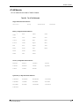
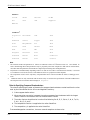
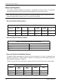
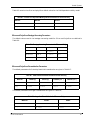
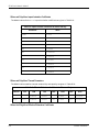
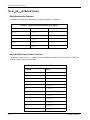
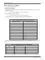
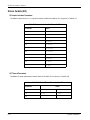
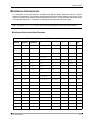
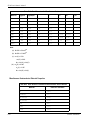
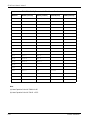
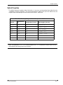
Appendix B:
Material Systems
Overview
ATLAS understands a library of materials for reference to material properties and models of various
regions in the semiconductor device. These materials are chosen to represent those most commonly
used by semiconductor physicists today. Users of BLAZE or BLAZE3D will have access to all of these
materials. S-PISCES or DEVICE3D users will have only access to Silicon and Polysilicon.
S-PISCES is designed to maintain backward compatibility with the standalone program SPISCES2
version 5.2. In the SPISCES2 syntax, certain materials could be used in the REGION statement just by
using their name as logical parameters. This syntax is still supported.
Semiconductors, Insulators and Conductors
All materials in ATLAS are strictly defined into three classes as either semiconductor materials,
insulator materials or conductors. Each class of material has particular properties to which all users
should be aware.
Semiconductors
All equations specified by the user’s choice of models are solved in semiconductor regions. All
semiconductor regions must have a band structure defined in terms of bandgap, density of states,
affinity etc. The parameters used for any simulation can be echoed to the run-time output using
MODELS PRINT. For complex cases with mole fraction dependent models these quantities can be seen
in Tonyplot by specifying OUTPUT BAND.PARAM and saving a solution file.
Any semiconductor region that is defined as an electrode is then considered to be a conductor region.
This is typical for polysilicon gate electrodes.
Insulators
In insulator materials only the Poisson and lattice heat equations are solved. Therefore for isothermal
simulations, the only parameter required for an insulator is dielectric permittivity defined using
MATERIAL PERM=<n>.
Materials usually considered as insulators (eg. SiO2) can be treated as semiconductors using BLAZE,
however all semiconductor parameters are then required.
Conductors
All conductor materials must be defined as electrodes. Conversely all electrode regions are defined as
conductor material regions. If a file containing regions of a material known to be a conductor are read
in, these regions will automatically become un-named electrodes. As noted bellow if the file contains
materials that are unknown, these region will become insulators.
During electrical simulation only the electrode boundary nodes are used. Nodes that are entirely
within an electrode region are not solved. Any quantities seen inside a conductor region in TONYPLOT
are spurious. Only optical ray tracing and absorption for LUMINOUS and lattice heating are solved
inside of conductor/electrode regions.
SILVACO International
B-1
ATLAS User’s Manual - Volume 2
Unknown Materials
If a mesh file is read containing materials not in Table B-1 these will automatically become insulator
regions with a relative permittivity of 3.9. All user-defined materials from ATHENA, irrespective of
the material name chosen by the user, will also become such insulator materials.
B-2
SILVACO International
Material Systems
ATLAS Materials
ATLAS materials are listed in Table B-1 below.
Table B-1. The ATLAS Materials
Single Element Semiconductors
Silicon1
Poly2
Germanium
Diamond
Binary Compound Semiconductors
3
GaP
CdSe
SnTe
SiGe
InP
CdTe
ScN
a-SiC
InSb
HgS
GaN
b-SiC
InAs
HgSe
AlN
AlP
ZnS
HgTe
InN
AlAs
ZnSe
PbS
BeTe
AlSb
ZnTe
PbSe
GaSb
CdS
PbTe
GaAs
Ternary Compound Semiconductors
AlGaAs
GaSbP
InAlAs
GaAsP
InGaAs
GaSbAs
InAsP
HgCdTe
InGaP
InGaN
AlGaN
Quaternary Compound Semiconductors
InGaAsP
AlGaAsP
AlGaAsSb
InAlGaN
InGaNAs
InGaNP
AlGaNAs
AlGaNP
AlInNAs
AlInNP
InAlGaAs
InAlGaP
InAlAsP
SILVACO International
B-3
ATLAS User’s Manual - Volume 2
Insulators
Vacuum
Oxide
Nitride
Si3N4
Air
SiO2
SiN
Sapphire
Palladium
TiW
TaSi
Aluminum
Cobalt
Copper
PaSi
Gold
Molybdenum
Tin
PtSi
Silver
Lead
Nickel
MoSi
AlSi
Iron
WSi
ZrSi
Tungsten
Tantalum
TiSi
AlSi
Titanium
AlSiTi
NiSi
Conductor
Platinum
AlSiCu
CoSi
Contact
Ambient
Conductors4
Polysilico
2
Notes
1.
The material models and parameters of Silicon are identical to those of S-PISCES version 5.2. Users should be
aware that although these band parameters may be physically inaccurate compared to bulk silicon measurements,
most other material parameters and models are empirically tuned using these band parameters.
2.
Polysilicon is treated differently depending on how it is used. In cases where it is defined as an electrode, it is treated
as a conductor. It can also be used as a semiconductor such as in a polysilicon emitter bipolars.
3.
The composition of SiGe is the only binary compound that can be varied to simulate the effects of band gap variations.
4.
Conductor names are only associated with electrodes. They are used for the specification of thermal conductivities
and complex index of refraction and for display in TonyPlot.
Rules for Specifying Compound Semiconductors
The rules for specifying the order of elements for compound semiconductors are derived from the rules
used by the International Union of Pure and Applied Chemistry:
1. Cations appear before anions.
2. When more than one cation is present the order progresses from the element with the largest
atomic number to the element with the smallest atomic number.
3. The order of anions should be the in order of the following list: B, Si, C, Sb, As, P, N, H, Te, Se,
S, At, I, Br, Cl, O, and F.
4. The composition fraction x is applied to the cation listed first.
5. The composition y is applied to the anion listed first.
To accomodate popular conventions, there are several exceptions to these rules.
B-4
SILVACO International
Material Systems
•SiGe: The composition fraction x applies to the Ge component. SiGe is then specified as Si(1-x)Ge(x),
an exception to rule #4.
•AlGaAs : This is specified as Al(x)Ga(1-x)As. This is an exception to rule #2.
•InGaAsP: The convention In(1-x)Ga(x)As(y)P(1-y) as set forth by Adachi is used. This is an exception to
rule #4.
SILVACO International
B-5
ATLAS User’s Manual - Volume 2
Silicon and Polysilicon
The material parameters defaults for Polysilicon are identical to those for Silicon. The following
paragraphs describe some of the material parameter defaults for Silicon and Polysilicon.
Note: Within the Physics section of this manual, a complete description is given of each model. The
parameter defaults listed in Chapter Three are all Silicon material defaults.
Silicon and Polysilicon Band Parameters
Table B-2. Band parameters for Silicon and Poly
Material
Eg300
eV
α
Nc300
per cc
β
χ
eV
Nv300
per cc
Silicon
1.08
4.73x10⁻⁴
636.0
2.8x10¹⁹
1.04x10¹⁹
4.17
Poly
1.08
4.73x10⁻⁴
636.0
2.8x10¹⁹
1.04x10¹⁹
4.17
Silicon and Polysilicon Dielectric Properties
Table B-3. Static dielectric constants for Silicon and Poly
Material
Dielectric Constant
Silicon
11.8
Poly
11.8
Silicon and Polysilicon Default Mobility Parameters
The default mobility parameters for Silicon and Poly are identical in all cases. The defaults used
depend on the particular mobility models in question. A full description of each mobility model and
their coefficients are given in Chapter 3.
Table B-4 contains the silicon and polysilicon default values for the low field constant mobility model.
Table B-4. Lattice Mobility Model Defaults for Silicon and Poly
Material
B-6
MUN
cm2/Vs
MUP
cm2/Vs
TMUN
TMUP
Silicon
1000.0
500.0
1.5
1.5
Poly
1000.0
500.0
1.5
1.5
SILVACO International
Material Systems
Table B-5 contains the silicon and polysilicon default values for the field dependent mobility model.
Table B-5. Parallel Field Dependent Mobility Model Parameters for Silicon and Poly
Material
BETAN
BETAP
Silicon
2
1
Poly
2
1
Silicon and Polysilicon Bandgap Narrowing Parameters
The default values used in the bandgap narrowing model for SIlicon and Polysilicon are defined in
Table B-6.
Table B-6. Bandgap Narrowing Parameters for Silicon and Poly
Statement
Parameter
Defaults
Units
MATERIAL
BGN.E
6.92x10⁻³
V
MATERIAL
BGN.N
1.3x10¹⁷
cm-3
MATERIAL
BGN.C
0.5
—
Silicon and Polysilicon Recombination Parameters
The default parameters for Schockley-Read-Hall recombination are given in Table B-7.
Table B-7. SRH Lifetime Parameter Defaults for Silicon and Poly
Material
TAUN0 (s)
TAUP0 (s)
NSRHN (cm-3)
NSRHP (cm-3)
Silicon
1.0x10⁻⁷
1.0x10⁻⁷
5.0x10¹⁶
5.0x10¹⁶
Poly
1.0x10⁻⁷
1.0x10⁻⁷
5.0x10¹⁶
5.0x10¹⁶
The default parameters for Auger recombination are given in Table B-8;
Table B-8. Auger Coefficient Defaults for Silicon and Poly
Material
AUGN
AUGP
Silicon
8.3x10⁻³²
1.8x10⁻³¹
Poly
8.3x10⁻³²
1.8x10⁻³¹
SILVACO International
B-7
ATLAS User’s Manual - Volume 2
Silicon and Polysilicon Impact Ionization Coefficients
The default values for the SELB impact ionization coefficients are given in Table B-9.
Table B-9. Impact Ionization Coefficients for Silicon and Poly
Parameter
Value
EGRAN
4.0x10⁵
BETAN
1.0
BETAP
1.0
AN1
7.03x10⁵
AN2
7.03x10⁵
BN1
1.231x10⁶
BN2
1.231x10⁶
AP1
6.71x10⁵
AP2
1.582x10⁶
BP1
1.693x10⁶
BP2
2.036x10⁶
Silicon and Polysilicon Thermal Parameters
The default values used for thermal conductivity and capacity are given in Table B-10.
Table B-10. Effective Richardson Coefficients for Silicon and Poly
Material
TCA
TCB
TCC
HCA
HCB
HCC
HCD
Silicon
0.03
1.56x10⁻³
1.65x10⁻⁶
1.97
3.6x10⁻⁴
0.0
-3.7x10⁴
Poly
0.03
1.56x10⁻³
1.65x10⁻⁶
1.97
3.6x10⁻⁴
0.0
-3.7x10⁴
Silicon And Polysilicon Effective Richardson Coefficients
B-8
SILVACO International
Material Systems
Table B-11. Effective Richardson Coefficients for Silicon and Poly
Material
ARICHN (A/cm2/K2)
ARICHP (A/cm2/K2)
Silicon
110.0
30.0
Poly
110.0
30.0
SILVACO International
B-9
ATLAS User’s Manual - Volume 2
The Al(x)Ga(1-x)As Material System
AlGaAs Recombination Parameters.
The default recombination parameters for AlGaAs are given in Table B-12.
Table B-12. Default Recombination Parameters for AIGaAs
Parameter
Value
Equation
TAUN0
1.0x10⁻⁹
3-213
TAUP0
1.0x10⁻⁸
3-213
COPT
1.5x10⁻¹⁰
3-226
AUGN
5.0x10⁻³⁰
3-227
AUGP
1.0x10⁻³¹
3-227
GaAs and AlGaAs Impact Ionization Coefficients.
The default values for the SELB impact ionization coefficients used for GaAs are given in Table B-13.
AlGaAs uses the same values as GaAs.
Table B-13. Impact Ionization Coefficients for GaAs
B-10
Parameter
Value
EGRAN
0.0
BETAN
1.82
BETAP
1.75
EGRAN
0.0
AN1
1.889x10⁵
AN2
1.889x10⁵
BN1
5.75x10⁵
BN2
5.75x10⁵
AP1
2.215x10⁵
AP2
2.215x10⁵
BP1
6.57x10⁵
BP2
6.57x10⁵
SILVACO International
Material Systems
AlGaAs Thermal Parameters.
The default thermal parameters used for AlGaAs are given in Table B-14.
Table B-14. Default Thermal Parameters for GaAs
Parameter
Value
TCA
2.27
HCA
1.738
GaAs Effective Richardson Coefficients.
The default values for the effective Richardson coefficients for GaAs are 6.2875 A/cm2/K2 for electrons
and 105.2 A/cm2/K2 for holes.
SILVACO International
B-11
ATLAS User’s Manual - Volume 2
The In(1-x)Ga(x)As(y)P(1-y) System
InGaAsP Thermal Parameters.
The default material thermal models for InGaAsP assumes lattice-matching to InP. The material
density is then given by;
ρ = 4.791 + 0.575 y.composition + 0.138 y.composition
The specific heat for InGaAsP is given by;
C p = 0.322 + 0.026 y.composition – 0.008 y.composition
The thermal resistivities of InGaAsP are linearly interpolated from Table B-15.
Table B-15. Thermal Resistivities for InGaAsP Lattice-Matched to InP
Composition Fraction y
Thermal Resistivity (deg(cm/w)
0.0
1.47
0.1
7.05
0.2
11.84
0.3
15.83
0.4
19.02
0.5
21.40
0.6
22.96
0.7
23.71
0.8
23.63
0.9
22.71
1.0
20.95
The default thermal properties of the binary compounds in the InGaAsP system are given in Table B16.
Table B-16. Default Thermal Properties of InP InAs GaP and GaAs
Material
B-12
Thermal Capacity (J/cm3)
Thermal Resistivity (deg(cm/W)
InP
1.543
1.47
InAs
1.994
3.70
GaP
1.292
1.30
GaAs
1.738
2.27
SILVACO International
Material Systems
The default thermal properties for the terniary compounds in the InGaAsP system: In(1-x)Ga(x)As,
In(1-x)Ga(x)P, InAs(y)P(1-y), and GaAs(y)P(1-y) are given, as a function of composition fraction, by linear
interpolations from these binary compounds.
SILVACO International
B-13
ATLAS User’s Manual - Volume 2
Silicon Carbide (SiC)
SiC Impact Ionisation Parameters
The default values for the SELB impact ionization coefficients used for SiC are given in Table B-17.
Table B-17. Impact Ionization Coefficients for SiC
Parameter
Value
EGRAN
0.0
BETAN
1.0
BETAP
1.0
AN1
1.66x10⁶
AN2
1.66x10⁶
BN1
1.273x10⁷
BN2
1.273x10⁷
AP1
5.18x10⁶
AP2
5.18x10⁶
BP1
1.4x10⁷
BP2
1.4x10⁷
SiC Thermal Parameters.
The default thermal parameters used for both 6H and 4H-SiC are shown in Table B-18.
Table B-18. Default Thermal Parameters for SiC
Parameter
B-14
Value
4H-SiC
6H-SiC
TCA
0.204
0.385
HCA
0
0
SILVACO International
Material Systems
Miscellaneous Semiconductors
The remainder of the semiconductors available have defined default parameter values to various
degrees of completeness. The following sections describe those parameter defaults as they exist. Since
many of the material parameters are not available at this time, it is recommended that care be taken
in using these materials. It is important to make sure that the proper values are used
Note: The syntax MODEL PRINT can be used to echo the parameters used to the run-time output.
Miscellaneous Semiconductor Band Parameters
Table B-19. Band Parameters for Miscellaneous Semiconductors
Material
Eg(0)eV
α
β
mc
mv
χeV
4.77x10⁻⁴
235.0
0.2225
0.2915
4.0
5.45
4.77x10⁻⁴
0.0
(a)
(b)
7.2
Eg(300)eV
Silicon
Polysilicon
Ge
0.7437
Diamond
6H-SiC
2.9
2.9
0.0
0.0
0.454
0.33
4H-SiC
2.2
2.2
0.0
0.0
0.41
0.165
A1P
2.43
2.43
0.0
0.0
A1As
2.16
2.16
0.0
0.0
A1Sb
1.6
2.69x10⁻⁴
2.788
(c)
0.4
GaSb
0.81
3.329x10⁻⁴
-27.6622
(c)
0.24
3.65
InSb
0.235
2.817x10⁻⁴
90.0003
0.014
0.4
4.06
ZnS
3.8
3.8
0.0
0.0
0.4
ZnSe
2.58
2.58
0.0
0.0
0.1
0.6
ZnTe
2.28
0.0
0.0
0.1
0.6
4.09
Cds
2.53
2.53
0.0
0.0
0.21
0.8
3.5
CdSe
1.74
1.74
0.0
0.0
0.13
0.45
4.5
CdTe
1.5
1.5
0.0
0.0
0.14
0.37
HgS
2.5
2.5
0.0
0.0
4.59
4.28
HgSe
HgTe
SILVACO International
B-15
ATLAS User’s Manual - Volume 2
Table B-19. Band Parameters for Miscellaneous Semiconductors
Material
Eg(0)eV
Eg(300)eV
α
β
mc
mv
PbS
0.37
0.37
0.0
0.0
0.25
0.25
PbSe
0.26
0.26
0.0
0.0
0.33
0.34
PbTe
0.29
0.29
0.0
0.0
0.17
0.20
SnTe
0.18
0.18
0.0
0.0
ScN
2.15
2.15
0.0
0.0
GaN
3.45
3.45
0.0
0.0
0.172
0.259
A1N
6.28
6.28
0.0
0.0
0.314
0.417
InN
1.89
1.89
0.0
0.0
0.11
0.17
BeTe
2.57
2.57
0.0
0.0
χeV
4.6
Notes
(a). Nc300 = 5.0x10¹⁸
(b). Nv300 = 1.8x10¹⁹
(c). mc(X) = 0.39
mc(G) = 0.09
Nc = Nc(X) + Nc(G)
(d). mc(G) = 0.047
mc(L) = 0.36
Nc = Nc(G) + Nc(L)
Miscellaneous Semiconductor Dielectric Properties
Table B-20. Static Dielectric Constants for Miscellaneous Semiconductors
Material
B-16
Dielectric Constant
Ge
16.0
Diamond
5.5
6H-SiC(a)
9.66
4H-SiC(b)
9.72
AlP
9.8
AlAs
12.0
AlSb
11.0
SILVACO International
Material Systems
Table B-20. Static Dielectric Constants for Miscellaneous Semiconductors
Material
Dielectric Constant
GaSb
15.7
InSb
18.0
ZnS
8.3
ZnSe
8.1
CdS
8.9
CdSe
10.6
CdTe
10.9
HgS
HgSe
25.0
HgTe
20.
PbS
170.0
PbSe
250.0
PbTe
412.0
SnTe
ScN
GaN
9.5
AlN
9.14
InN
19.6
BeTe
Miscellaneous Semiconductor Mobility Properties
Table B-21. Mobility Parameters for Miscellaneous Semiconductors
Material
MUNO (cm2/Vs)
MUPO (cm2/Vs)
Ge
3900.0(a)
1900.0(b)
Diamond
500.0
300.0
2.0x10⁷
SiC(a)
330.0
300.0
2.0x10⁷
SiC(b)
1000.0
50.0
2.0x10⁷
AlP
80.0
SILVACO International
VSATN(cm/s)
VSAT(cmcm/s)
B-17
ATLAS User’s Manual - Volume 2
Table B-21. Mobility Parameters for Miscellaneous Semiconductors
Material
MUNO (cm2/Vs)
MUPO (cm2/Vs)
AlAs
1000.0
100.0
AlSb
200.0
550.0
GaSb
4000.0
1400.0
InSb
7800.0
750.0
ZnS
165.0
5.0
ZnSe
100.0
16
CdS
340.0
50.0
CdSe
800.0
CdTe
1050.0
VSATN(cm/s)
VSAT(cmcm/s)
100.0
HgS
HgSe
5500.0
HgTe
22000.0
100.0
PbS
600.0
700.0
PbSe
1020.0
930.0
PbTe
6000.0
4000.0
400.0
8.0
SnTe
ScN
GaN
AlN
InN
2.0x10⁷
14.0
3000.0
BeTe
Notes
(a) Uses Equation B-4 with TMUN=1.66.
(b) Uses Equation B-4 with TMUP = 2.33.
B-18
SILVACO International
Material Systems
Insulators
The default material parameters for insulator materials are given in the following sections. As noted
in the “Semiconductors, Insulators and Conductors” section the only parameter required for electrical
simulation in insulator materials is the the dielectric constant .Thermal and optical properties are
required in GIGA and LUMINOUS respectively.
Insulator Dielectric Constants
Table B-22. Default Static Dielectric Constants of Insulators
Material
Dielectric Constant
Vacuum
1.0
Air
1.0
Ambient
1.0
Oxide
3.9
Si02
3.9
Nitride
7.5
SiN
7.5
Si3N4
7.55
Sapphire
12.0
Insulator Thermal Properties
Table B-23. Default Thermal Parameters for Insulators
Material
Thermal Capacity (J/cm3)
Thermal Conductivity(deg(cm/W)
Vacuum
0.0
0.0
Air
1.0
0.026
7
Ambient
1.0
0.026
7
Oxide
3.066
0.014
4
Si02
3.066
0.014
4
Nitride
0.585
0.185
4
SILVACO International
Reference
B-19
ATLAS User’s Manual - Volume 2
Table B-23. Default Thermal Parameters for Insulators
Material
Thermal Capacity (J/cm3)
Thermal Conductivity(deg(cm/W)
Reference
SiN
0.585
0.185
4
Si3N4
0.585
0.185
4
Sapphire
B-20
SILVACO International
Material Systems
Optical Properties
The default values for complex index of refraction in LUMINOUS are interpolated from tables from the
“Handbook of Optical Constants,” first and second editions. Rather than print the tables here, the
ranges of optical wavelengths for each material are listed in Table B-24.
Table B-24. Wavelength Ranges for Default Complex Index of Refraction
Material
Temperature(
K)
Composition Fraction
Wavelengths (microns)
Silicon
300
NA
0.0103-2.0
AlAs
300
NA
0.2213 - 50.0
GaAs
300
NA
0.0 - 0.9814
InSb
300
NA
0.2296 - 6.5
InP
300
NA
0.1689 - 0.975
Poly
300
NA
0.1181 - 18.33
SiO2
300
NA
0.1145 - 1.7614
Note: The parameter INDEX.CHECK can be added to the SOLVE statement to list the values of real
and imaginary index being used in each solution.
SILVACO International
B-21
ATLAS User’s Manual - Volume 2
User Defined Materials
The current version of ATLAS does not directly support user defined materials. A simple workaround
can be done using the already existing user specifications. This workaround is based on the use of an
already existing material name and modifying the material parameters as appropriate.
In ATLAS material names are defined to give the user a reasonable set of default material parameters.
Any of these defaults can be overriden using the MATERIAL, IMPACT, MODEL, and MOBILITY
statements. The key to defining new materials is choosing a material name that is defined in ATLAS,
then modifying the material parameters of that material to match the user material. Here it is best to
choose a material that has default parameter values that might best match the user material, while
being sure to choose a material that is not already in the user device. Next the user must associate this
material name with the device regions where the new material is present. This is done by either
specifying the chosen material name on the appropriate REGION statements (when the device is
defined in the ATLAS syntax) or choosing the material name from the materials menu when defining
the region in DEVEDIT.
Next, the user should modify the material statements using MATERIAL, IMPACT, MOBILITY, and
MODEL statements. When doing this the MATERIAL parameter of the given statement should be
assigned to the chosen material name.
For materials with variations in composition fraction, the user should choose a defined material with
X and/or Y composition fractions (i.e., a terniary or quaterniary material). The user may also find it
convenient to use C interpreter functions to define the material parameters as a function of
composition. The C interpreter functions that are useful for this approach are: F.MUNSAT,
F.MUPSAT, F.BANDCOMP, F.VSATN, F.VSATP, F.RECOMB, F.INDEX, F.BGN, F.CONMUN,
F.CONMUP, F.COPT, F.TAUN, F.TAUP, F.GAUN, and F.GAUP.
In defining new materials there exists a minimum set of parameters that should be defined. This set
includes bandgap (EG300), electron and hole density of states (NC300 and NV300), dielectric
permitivity (PERMITIVITY), and electron and hole mobilities (MUN and MUP). For bipolar devices
certain recombination parameters should also be defined such as: lifetimes (TAUN and TAUP), radiative
recombination rates (COPT), and Auger coefficients (AUGN and AUGP). For devices with variations
in material composition certain band-edge alignment parameters should also be defined: either
electron affinity (AFFINITY) or edge alignment (ALIGN). If impact ionization is considered the impact
ionization coefficients should also be defined.
As an example, consider the case where the user is simulating a device with an AlInGaP region.
Consulting table B-1, we see that this material system is not defined in ATLAS. We then choose a
materal that is defined in ATLAS which has default material parameters that best approximate the
material parameters of the new material. In this case, we choose InGaAsP since, at least for example
purposes, we feel that this material is closest to the AlInGaP. Next, we must specify InGaAsP as the
material of the region(s) that is/are composed of AlInGaP. This can be done either on the REGION
statement if the structure is defined in ATLAS syntax or from the material menu when the region is
defined in DEVEDIT.
Supposing that we are satisfied with the default values of the parameters from the "minimum set"
discussed above, and that we are principally concerned with the recombination and heat flow
parameters defaults, the following section of the input deck illustrates how these parameter defaults
may be modified:
# new material AlInGaP
MATERIAL MATERIAL=InGaAsP
# SRH
MATERIAL MATERIAL=InGaAsP TAUN0=1.1e-9 TAUP0=2.3e-8
# Auger
MATERIAL MATERIAL=InGaAsP AUGN=5.8e-30 AUGP=1.1e-31
# Optical
material material=InGaAsP COPT=1.7e-30
B-22
SILVACO International
Material Systems
# Thermoconductivity
MATERIAL MATERIAL=InGaAsP TC.A=2.49
# Heat capacity
MATERIAL MATERIAL=InGaAsP HC.A=1.9
SILVACO International
B-23
ATLAS User’s Manual - Volume 2
B-24
SILVACO International