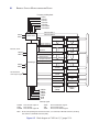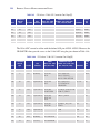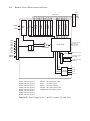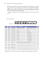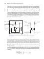
1
An Introduction to Computer Engineering using the Renesas Sakura Microcontroller Board BY JAMES M. CONRAD Micrim Press 1290 Weston Road, Suite 306 Weston, FL 33326 USA www.micrium.com Designations used by companies to distinguish their products are often claimed as trademarks. In all instances where Micrim Press is aware of a trademark claim, the product name appears in initial capital letters, in all capital letters, or in accordance with the vendor’s capitalization preference. Readers should contact the appropriate companies for more complete information on trademarks and trademark registrations. All trademarks and registered trademarks in this book are the property of their respective holders. Copyright © 2014 by James M. Conrad except where noted otherwise. Published by Micrim Press. All rights reserved. Printed in the United States of America. No part of this publication may be reproduced or distributed in any form or by any means, or stored in a database or retrieval system, without the prior written permission of the publisher; with the exception that the program listings may be entered, stored, and executed in a computer system, but they may not be reproduced for publication. The programs and code examples in this book are presented for instructional value. The programs and examples have been carefully tested, but are not guaranteed to any particular purpose. The publisher and content contributors do not offer any warranties and does not guarantee the accuracy, adequacy, or completeness of any information herein and is not responsible for any errors or omissions. The publisher and content contributors assume no liability for damages resulting from the use of the information in this book or for any infringement of the intellectual property rights of third parties that would result from the use of this information. Library of Congress subject headings: 1. Embedded computer systems 2. Real-time data processing 3. Computer software—Development For bulk orders, please contact Micriµm Press at: ⫹1 954 217 2036 ISBN: 978-1-935772-92-7 Please report errors or forward any comments and suggestions to [email protected]. Preface This book is the result of a long relationship the author has enjoyed with Renesas Electronics America, Inc. (and one of its predecessors, Mitsubishi Electronics). I originally worked with this company because of their commitment to providing a low-cost evaluation board and free development software that students could purchase and use in classes and senior design projects. Over the years the boards have remained as affordable (and popular) as ever, and the software development tools available have added more functionality while still available for free to our students. I have been teaching embedded systems courses for over fourteen years (and working in the field even longer). I had not been able to find a book suitable for using in an Introduction to Computer Engineering course that would lend itself to the theoretical and applied nature of the discipline and embedded systems design. When Renesas released the GR-SAKURA board, I knew I have the perfect platform to use in the course. This book was developed to augment the hands-on exercises we use. This book also has a radical feature not seen in many books currently on the market (if any). It is freely available for download. It is also available for purchase in hardcopy form for a modest price. This book would not have been possible had it not been for the assistance of numerous people. Several students and educators contributed to and extensively tested some of the chapters, including: Yevgeny Fridlyand (2, 3, 4), Adam Harris (1, 2, 3), Anthony Harris (3), Onkar Raut (2, 4) Suganya Jebasingh (2, 4), and Steven Erdmanczyk (4) . Thanks go to the publisher, Linda Foegen, and especially June Harris, Rob Dautel and Todd DeBoer of Renesas for their help in getting this book produced and published (and for their patience!). Many, many thanks go to the reviewers who offered valuable suggestions to make this book better, especially David Brown and students from my UNC Charlotte Introduction to Engineering and Embedded Systems courses. I would like to personally thank my parents, the Conrads, and my in-laws, the Warrens, for their continued assistance and guidance through the years while I worked on books. Also, I would especially like to thank my children, Jay, Mary Beth, and Caroline, and my wife Stephanie for their understanding when I needed to spend more time on the book than I spent with them. James M. Conrad, March 2014 iii Foreword For more than a decade the microcontroller world has been dominated by the quest for ultra-low power, high performance devices—two goals that are typically mutually exclusive. The Renesas RX MCU quickly achieved market leadership by achieving both of these goals with a highly innovative architecture. The RX family enables embedded designs that previously would have required some uncomfortable tradeoffs. However there are no simple solutions to complex problems, and mastering all of the RX63N’s features is not a task to be undertaken lightly. Fortunately in this book Dr. Conrad, has crafted a guidebook for embedded developers that moves smoothly from concepts to coding in a manner that is neither too high level to be useful nor too detailed to be clear. It explains beginning software engineering techniques and shows how to implement them in RX63N-based applications, moving from a clear explanation of problems to techniques for solving them to line-by-line explanations of example code. Modern embedded applications increasingly require hardware/software co-design, though few engineers are equally conversant with both of these disciplines. In this book the author takes a holistic approach to design, both explaining and demonstrating just how software needs to interact with Sakura hardware. Striking a balance between breadth and depth it should prove equally useful and illuminating for both hardware and software engineers. Whether you are a university student honing your design skills, a design engineer looking for leading edge approaches to time-critical processes, or a manager attempting to further your risk management techniques, you will find Jim’s approach to embedded systems to be stimulating and compelling. Peter Carbone Renesas v Contents Preface iii Foreword v CHAPTER 1 Introduction to Embedded Systems 1 1.1 Learning Objectives 1 1.2 Concepts 1 1 2 1.2.1 1.2.2 1.3 Economics and Microcontrollers Embedded Networks Typical Benefits of Embedded Systems 1.3.1 1.3.2 1.3.3 1.3.4 Greater Performance and Efficiency Lower Costs More Features Better Dependability 2 3 3 4 4 1.4 Embedded System Functions 4 1.5 Attributes of Embedded Systems 5 1.6 Constraints on Embedded Systems 6 1.7 Developing Embedded Systems 6 7 8 9 1.7.1 1.7.2 1.7.3 Product Development Designing and Manufacturing Embedded Systems The Role of a Computer Engineer 1.8 An Example of an Embedded System: The Renesas Sakura Board 10 1.9 Summary of Book Contents 10 1.10 Recap 10 1.11 References 11 vii viii CONTENTS CHAPTER 2 Introduction to Software Development 13 2.1 Learning Objectives 13 2.2 Computer Organization & Architecture 13 Microcontroller Basics 16 16 17 2.3 2.3.1 2.3.2 2.3.3 2.4 Port Direction Register (PDR) 17 Set Switch 1 (Port A bit 7) as Input 18 Port Output Data Register (PODR) 18 Set LED0 (Port A bit 0) as Output 19 Sets LEDs 1, 2, 3, and 4 (Port A bit 0, 1, 2, and 3) as Outputs 19 Port Input Data Register (PIDR) 19 Port Mode Register (PMR) Data Types Software Development Tools 2.4.1 2.4.2 2.4.3 2.4.4 2.5 Bits and Bytes Ports Compilation Mechanism Compilers for Embedded Systems Debugger Example of an Integrated Development Environment Basic Software Development 2.5.1 2.5.2 2.5.3 2.5.4 2.5.5 2.5.6 Development Lifecycle Overview Define System Requirements Requirements—Robotics Applications Developing Code Start with an Algorithm Convert your Algorithms to Code 20 20 22 22 23 24 24 26 26 27 29 30 30 31 2.6 Recap 33 2.7 References 33 2.8 Exercises 33 CONTENTS ix CHAPTER 3 Getting Started with GR-Sakura 35 3.1 Learning Objectives 35 3.2 Sakura Embedded System 35 35 38 3.2.1 3.2.2 Sakura Board Design Basic Concepts of the RX63N Microprocessor 3.3 Sakura Software Development 44 3.4 Sakura Example Project 46 3.5 Updating the GR-Sakura Firmware 50 3.6 Setting Up an Account with MyRenesas 54 3.7 BASIC Motor & Sensor Control 57 57 3.7.1 3.7.2 3.8 Switch Controlled LEDs Using LEDs as Outputs 58 Using Switches as Inputs Driving Motors and Coils 58 61 Basic Robotics Application 3.8.1 3.8.2 3.8.3 Motor Robot Kit Assembly Understanding the Hardware Developing Code 63 63 68 72 3.9 Recap 75 3.10 References 75 3.11 Exercises 76 CHAPTER 4 Interfacing with the Outside World 77 4.1 Learning Objectives 77 4.2 Event Counters and Timers 77 Event Counter 78 x CONTENTS 4.2.1 4.2.2 4.2.3 4.2.4 4.2.5 4.2.6 4.2.7 4.3 Setting Up a Timer for Counting Events Timer Count Register 81 Timer Counter Control Register 81 Time Constant Register 83 Timer Control/Status Register 84 Timer Control Register Cascading Timers Using Interrupts as Event Counters 85 87 92 void interrupts (void) 93 void noInterrupts (void) 93 void detachInterrupt (unsigned char interrupt) 93 interrupt—number (0–7) 93 void attachInterrupt (unsigned char interrupt, void (*) (void) func, int mode) 94 interrupt—numbers (0–7) Setting Up a Timer for Pulse Output Setting up Timer interrupts for Pulse Output Frequency and Period Control Advanced Motor Control: Robotics Application 108 4.2.7.2 Using Interrupts—Pulse output & Counters 112 10-Bit ADC Input Pins 4.3.2 4.3.3 4.3.4 94 97 101 105 106 4.2.7.1 Using Timers—Counters & Pulse Output Analog To Digital Converters 4.3.1 81 A/D Data Registers (ADDRn) (n ⫽ A to H) Initializing the 10-bit A/D Converter 117 122 122 125 126 Module Stop Control Register A (MSTPCRA) 126 A/D Control/Status Register (ADCSR) 127 A/D Control Register (ADCR) 129 A/D Control Register 2 (ADCR2) 10-bit A/D Conversion A/D Sensors: Robotics Application 129 132 135 4.3.4.1 Using Timers—Counters & Pulse Output 139 4.3.4.2 Using Interrupts—Pulse Output & Counters 143 CONTENTS xi 4.4 Recap 147 4.5 References 147 4.6 Exercises 147 Index 149 Chapter 1 Introduction to Embedded Systems 1.1 LEARNING OBJECTIVES In this chapter the reader will learn: 䡲 䡲 䡲 䡲 1.2 What an embedded system is Why to embed a computer What functions and attributes embedded systems need to provide What constraints embedded systems have CONCEPTS An embedded system is an application-specific computer system which is built into a larger system or device. Using a computer system rather than other control methods (such as non-programmable logic circuits, electro-mechanical controls, and hydraulic controls) offers many benefits such as sophisticated control, precise timing, low unit cost, low development cost, high flexibility, small size, and low weight. These basic characteristics can be used to improve the overall system or device in various ways: 䡲 䡲 䡲 䡲 Improved performance More functions and features Reduced cost Increased dependability Because of these benefits, billions of microcontrollers are sold each year to create embedded systems for a wide range of products. 1.2.1 Economics and Microcontrollers Microcontrollers are remarkably inexpensive yet offer tremendous performance. The microprocessor for a personal computer may cost $100 or more, while microcontrollers typically cost far less, starting at under $0.25. Why is this so? 1 2 RENESAS SAKURA MICROCONTROLLER BOARD Microcontrollers provide extremely inexpensive processing because they can leverage economies of scale. MCUs are programmable in software, so a chipmaker can design a single type of MCU which will satisfy the needs of many customers (when combined with their application-specific software). This reduces the per-chip cost by amortizing the design costs over many millions of units. The cost of an integrated circuit (such as a microcontroller or a microprocessor) depends on two factors: non-recurring engineering (NRE) cost and recurring cost. The NRE cost includes paying engineers to design the integrated circuit (IC) and to verify through simulation and prototyping that it will work properly. The recurring cost is incurred by making each additional IC, and includes raw materials, processing, testing, and packaging. The IC’s area is the major factor determining this recurring cost. The smaller the IC, the more will fit onto a silicon wafer and the lower the recurring cost. Microcontrollers are much smaller than microprocessors for personal computers, so they will cost less (given the same number of ICs sold). The NRE cost must be divided across each IC sold. As the number of ICs sold rises, the NRE adder falls, so each IC’s price falls as well. Because of this, low volume chips are more expensive than high-volume chips. 1.2.2 Embedded Networks Some embedded systems consist of multiple embedded computers communicating across an embedded network, and offer further benefits. Each computer on the network uses a communication protocol to share the same set of wires to communicate, rather than dedicating one set for each possible communication route. Several advantages come from having fewer wires: 䡲 䡲 䡲 Lower parts cost, as fewer wires are needed Lower labor costs, as it is faster to assemble Greater reliability, as it has fewer connections to fail Other advantages come from allowing separate nodes to share information. New features may be possible, or the system efficiency may be improved through better coordination of activities among different nodes. 1.3 TYPICAL BENEFITS OF EMBEDDED SYSTEMS As an example, let’s examine how embedded systems have affected automobiles. A typical modern car has dozens of microcontrollers embedded within it. Let’s see why. CHAPTER 1 / INTRODUCTION TO EMBEDDED SYSTEMS 1.3.1 3 Greater Performance and Efficiency Computer control of automobile engines lowers pollution and increases fuel efficiency, reducing operating costs. Burning gasoline with air in spark ignition engines is a tricky business if we want to maximize efficiency, yet minimize pollution. The main factor affecting emissions is the ratio of air mass to fuel mass. The ideal ratio is 14.7 to 1, and the catalytic converter is designed to operate most efficiently at this ratio. If there is too little air (a rich mix), then excessive carbon monoxide (CO) and hydrocarbons (HC) will be produced. If there is too much air (a lean mix), then large amounts of oxides of nitrogen (called NOx) will be created. So we would like for each fuel injector to add just the right amount of fuel. This depends on the mass of the air inside the cylinder, which depends on factors such as air temperature and air pressure. These in turn depend on altitude and weather, as well as whether the engine is warmed up or not. Another factor is the timing of the sparkplug firing. If it fires early, then there is more time for combustion within the cylinder before the exhaust valve opens. This raises the average temperature within the cylinder and changes the combustion process, affecting CO, HC, and NOx concentrations. It would be quite impractical to design a mechanical control system to consider all of these factors and squirt the fuel injectors at just the right instant for the right amount of time. Thankfully, an inexpensive microcontroller is quite effective at these kinds of calculations and control. 1.3.2 Lower Costs There are various ways in which an embedded system can reduce the costs associated with a device. 䡲 䡲 䡲 䡲 Component costs: Embedded software can compensate for poor signal quality, allowing the use of less-expensive components. For example, a low-cost pressure sensor may be very temperature-dependent. If ambient temperature information is already available, then it is a simple matter to compensate for the temperature induced error. Manufacturing costs: Many vehicles use the Control Area Network (CAN) protocol to communicate across an in-car network. The embedded network reduces assembly and parts costs because of the simpler wiring harness. Operating costs: As mentioned above, an embedded system enables automobile engines to operate more efficiently, reducing the amount of gasoline needed and hence lowering operating costs. Maintenance costs: Some vehicles predict oil life by monitoring engine use history, notifying the driver when an oil change is needed. 4 RENESAS SAKURA MICROCONTROLLER BOARD 1.3.3 More Features An MCU running application-specific software offers tremendous opportunities for features and customization. These features can make your company’s products stand out from the competition. 䡲 䡲 䡲 䡲 1.3.4 Cruise control keeps the car running at the same speed regardless of hills, wind, and other external factors. Smart airbags reduce injuries by adjusting inflation speed based on passenger weight. Power seats move to each driver’s preferred position automatically, based on whose keyless entry fob was used to open the car. Headlights and interior lights shut off automatically after a time delay if the car is not running and prevents the lights from draining the battery. Better Dependability Embedded systems and networks offer many opportunities to improve dependability. 䡲 䡲 䡲 1.4 An engine controller (and other controllers) can provide various “limp-home modes” to keep the car running even if one or more sensors or other devices fail. A warning of an impending failure can be provided. Diagnostic information can be provided to the driver or service personnel, saving valuable trouble-shooting time. EMBEDDED SYSTEM FUNCTIONS There are several common functions which embedded systems typically provide. 䡲 䡲 Control systems monitor a process and adjust an output variable to keep the process running at the desired set point. For example, a cruise control system may increase the throttle setting if the car’s speed is lower than the desired speed, and reduce it if the car is too fast. There is often sequencing among multiple states. For example, a car engine goes through multiple states or control modes when started. During Crank and Start, the fuel/air mix is rich and depends on the engine coolant temperature. Once the engine has started, the controller switches to the Warm-Up mode, in order to raise the engine and exhaust system temperatures to their ideal levels. Here the fuel/air mixture and ignition timing are adjusted, again based in part on the engine coolant CHAPTER 1 / INTRODUCTION TO EMBEDDED SYSTEMS 䡲 䡲 1.5 5 temperature. When the engine has warmed up it can switch into Idle mode. In this mode the controller seeks to minimize the engine’s speed, yet still run smoothly and efficiently despite changes in loads due to air conditioning, power steering, and the electrical system. Signal processing modifies input signals to eliminate noise, emphasize signal components of interest, and compensate for other factors. For example, a hands free speakerphone interface may use multiple microphones, beam-forming, and active noise cancellation to filter out low-frequency road noise. Other sensors may have spark-plug noise filtered out. Communications and networking enable different devices on the same network to exchange information. For example, the engine controller may need to send a message indicating speed. To do this, the speed value must be formatted according to the communication protocol and then loaded into the network interface peripheral for transmission. ATTRIBUTES OF EMBEDDED SYSTEMS Embedded systems are designed so that the resulting device behaves in certain desirable ways. 䡲 䡲 䡲 䡲 Embedded systems need to respond to events which occur in the environment, whether a user presses a button or a motor overheats. A system which is not sufficiently responsive is not likely to be a successful product. For example, when we press a channel select button for the radio, we would like for it to respond within some reasonable time. For real-time systems, the timing of the responses is critical because late answers are wrong answers. Igniting the fuel in a cylinder is time-critical because bad timing can damage or destroy engine components (to say nothing of reducing power, or the efficiency and pollution concerns mentioned previously). Embedded systems typically require sophisticated fault handling and diagnostics to enable safe and reliable operation. Often the fault handling code is larger and more complex than the normal operation code. It is easy to design for the “everything goes right and works fine” case. It is far more difficult to determine methods to handle the exceptional cases. What is likely to fail? Which failures can lead to dangerous conditions? How should the system handle failures? How will you test that the system handles the failures correctly? Embedded systems may be expected to operate independently for years without operator attention such as adjustment or resetting. The system is expected to operate robustly and always work. Given that it is very difficult and expensive to write perfect, bug-free software, developers build in mechanisms to detect faulty behavior and respond, perhaps by restarting the system. 6 RENESAS SAKURA MICROCONTROLLER BOARD 1.6 CONSTRAINTS ON EMBEDDED SYSTEMS Embedded systems often have constraints which limit the designer’s options, and can lead to creative and elegant solutions. These constraints are typically different from those for general-purpose computers. 䡲 䡲 䡲 䡲 1.7 Cost is a common constraint. Many applications which use embedded systems are sold in very competitive markets, in which price is a major factor. Often a manufacturer will hire subcontractors to design and build individual sub-systems. This allows the manufacturer to pit potential subcontractors against each other, keeping prices down. There may be size and weight limits for portable and mobile applications. An embedded system for an automotive remote keyless entry transmitter must fit into a small fob on a key ring which fits easily into a pocket. Similarly, the receiver must not be too heavy. A heavier car will have worse acceleration, braking, cornering, and fuel efficiency. Aircraft and spacecraft are especially sensitive to weight since a heavier craft requires more fuel to achieve the same range. There may be limited power or energy available. For example, a battery has a limited amount of energy, while a solar cell generates a limited amount of power. High temperatures may limit the amount of cooling available, which will limit the power which can be used. The environment may be harsh. Automotive electronics under the hood of a car need to operate across a wide range of temperatures (⫺40°C to 125°C, or ⫺40°F to 193°F), while withstanding vibrations, physical impact, and corroding salt spray. Spark plugs generate broadband radio frequency energy which can interfere with electronics. DEVELOPING EMBEDDED SYSTEMS So, who develops embedded systems? There are many different people who contribute to a final embedded systems product. These include engineers and scientists who: 䡲 䡲 䡲 䡲 create the basic technological advances in materials (Scientists) design the device enclosure (Mechanical Engineers) design the circuit boards and components on the circuit boards (Electrical Engineers) design and write code which interfaces with the user and performs the specific device application (Software Engineers) CHAPTER 1 / INTRODUCTION TO EMBEDDED SYSTEMS 䡲 䡲 䡲 7 design and write software to control the hardware (Computer Engineers) design the assembly lines which make the devices (Manufacturing and Industrial Engineers) make sure the mechanical, electrical, and computer components of a device work together (Systems Engineers) It should be noted that many other people can be considered embedded systems developers. There are countless students and hobbyist who create embedded systems used in robots, and entrepreneurs who create the next hot electronic toy. 1.7.1 Product Development Engineering design is the creative process of identifying needs and then devising a solution to fill those needs. This solution may be a product, a technique, a structure, a project, a method, or many other things, depending on the problem. The general procedure for completing a good engineering design can be called the Engineering Method of Creative Problem Solving. Problem solving is the process of determining the best possible action to take in a given situation. The types of problems that engineers must solve vary between and among the various branches of engineering. Because of this diversity, there is no universal list of procedures that will fit every problem. Not every engineer uses the same steps in his or her design process. The following list includes most of the steps that engineers use [1]: 1. 2. 3. 4. 5. 6. 7. 8. Identifying the problem Gathering the needed information Searching for creative solutions Overcoming obstacles to creative thinking Moving from ideas to preliminary designs (including modeling and prototyping) Evaluating and selecting a preferred solution Preparing reports, plans, and specifications (Project Planning) Implementing the design (Project Implementation) Often steps five through eight are expanded into more detailed steps, including: 䡲 䡲 䡲 Requirements gathering and specification of the entire product High-level design (architecture of the system) Low-level design (algorithms of the software modules and schematic capture of the electrical circuits) 8 RENESAS SAKURA MICROCONTROLLER BOARD 䡲 䡲 䡲 䡲 䡲 䡲 Coding and building the hardware (implementation) Unit testing of the individual software modules Functional testing (build the entire software package) Integration testing (put the software in the hardware) Verification and Beta testing (make sure it is compliant) Ship it! Engineers developing an embedded system will use these steps to conceive, plan, design, and build their products. 1.7.2 Designing and Manufacturing Embedded Systems Embedded systems are designed with a central microcontroller and other supporting electronic components mounted on a printed circuit board (PCB). PCBs provide the means to connect these integrated circuits to each other to make an operational system. The PCB provides structural support and the wiring of the circuit. The individual wires on the PCB are called traces and are made from a flat copper foil. While many circuit designs may use the same standard components, the PCB is often a custom component for a given design. Designing a PCB requires a completed schematic for the circuit. This schematic is sometimes different than the schematic seen in textbooks. It often contains extra information about the components and construction of the board. For example, a textbook schematic may only show a battery for the power supply, while the production schematic would show the battery case, the number of cells, the rating of the battery, and the manufacturers of the components. From the schematic, a designer will use their computer-aided design tools to identify the size of the PCB, and then place the electronic components on their board drawing. The designer will also place the wiring between the components on the PCB. The physical PCB is manufactured from a fiberglass-resin material that is lightweight and inexpensive. A manufacturer will add copper wiring traces to the surfaces of the board and the appropriate insulation and white silk screening. The final manufacturing steps are applying solder, placing the components, and heating/cooling the solder. Figure 1.1 shows an example of a finished board. The completed boards are electrically tested for functionality. Any board failing the test is inspected in more detail to find the problems. These boards are repaired to increase the passing rate acceptable to the manufacturer. The boards are wrapped in antistatic materials and shipped to the next location for the next stage of production, or immediately installed in a mechanical enclosure (like the mechanical shell of a mobile phone). CHAPTER 1 / INTRODUCTION TO EMBEDDED SYSTEMS 9 Figure 1.1 Renesas Sakura Board [2]. 1.7.3 The Role of a Computer Engineer Computer engineers work on the interface between different pieces of hardware and strive to provide new capabilities to existing and new systems or products. Computer engineers are concerned with the design, development, and implementation of computer technology into a wide range of consumer, industrial, commercial, and military applications. They might work on a system such as a flexible manufacturing system or a “smart” device or instrument. The work of a computer engineer is grounded in the hardware—from circuits to architecture—but also focuses on operating systems and software. Computer engineers must understand logic design, microprocessor system design, computer architecture, computer interfacing, and continually focus on system requirements and design. Computer Engineers must have strong analytical stills and be detail oriented. In addition, they must work well in team situations as they are often called upon to work in a group setting with other engineers and with others outside of engineering. Communication abilities are important because engineers often interact with specialists in a wide range of fields outside engineering. Computer Engineers are key contributors to the development of embedded systems since they have extensive knowledge of the hardware AND software of the system. The can 10 RENESAS SAKURA MICROCONTROLLER BOARD perform many of the tasks needed such as designing the circuitry, programming the operating system, or writing the supplication software. 1.8 AN EXAMPLE OF AN EMBEDDED SYSTEM: THE RENESAS SAKURA BOARD The Renesas Sakura Board (Figure 1.1) is one example of a Renesas MCU-based embedded system. This device has fifty-five digital I/O lines that are controlled by the Renesas microcontroller [2]. Some of the main components to note are the 100/10 Mbps Ethernet port in the upper left, a micro USB port right beneath the Ethernet port which is used to program the built-in flash memory, and at the bottom left a 5V DC power jack. The Sakura also has a micro SD card slot located on the underside of the board. The large chip in the center is a Renesas R5F563NBDDFP microcontroller from the RX Family of chips with 1024 K of flash memory, 128 K of RAM, and 32 K of data flash. Fifty-five I/O pins are used to interface with external pins on the module. This processor runs at 96 MHz [3]. 1.9 SUMMARY OF BOOK CONTENTS This book is structured as follows: 䡲 䡲 䡲 1.10 Chapter 2 shows how software is built. At the low level it shows how programs are compiled and downloaded. At the high level it shows software engineering concepts and practices. Chapter 3 presents an introduction to embedded systems development through basic concepts such as LEDs, switches, and motor control using the GR Sakura Embedded development board and associated tools. These concepts are demonstrated using a simple robotic vehicle platform. Chapter 4 presents how to use peripherals to interface with the environment and simplify programs. RECAP An embedded system is an application-specific computer system which is built into a larger system or device. Using a computer system enables improved performance, more functions and features, lower cost, and greater dependability. With embedded computer systems, manufacturers can add sophisticated control and monitoring to devices and other systems, while leveraging the low-cost microcontrollers running custom software. CHAPTER 1 / INTRODUCTION TO EMBEDDED SYSTEMS 1.11 11 REFERENCES [1] Wright, Paul H. (2002). Introduction to Engineering, Third Edition. John Wiley & Sons, Inc: New York. [2] Renesas. (2013). Gadget Renesas. Renesas Electronics America, Inc. Web. Accessed at http://www.renesas.com/products/promotion/gr/index.jsp#board [3] Renesas Electronics, Inc. (February, 2013). RX63N Group, RX631 Group User’s Manual: Hardware, Rev 1.60. Chapter 2 Introduction to Software Development 2.1 LEARNING OBJECTIVES This book cannot cover all of the concepts of embedded system design and microcontroller programming. There are, however, some basic concepts that are important. In this chapter the reader will learn about: 䡲 䡲 䡲 䡲 2.2 Basic organization of computers Basic representation of data in a computer Concepts of compiling code for an embedded system Concepts of developing software for an embedded system COMPUTER ORGANIZATION & ARCHITECTURE A computer is a complex digital system. The best way to look at it is by looking at its hierarchical nature. Hierarchical systems are best described as a series of subsystems that are interconnected at various levels to form a complete computer system. At each level is a set of components whose behavior depends on the characteristics and functions of the next lower level. A designer focuses on structure and function within each level. The computer has four basic functions to perform (see Figure 2.1): 1. 2. 3. 4. Data processing Data storage Data movement Data control Computers process data with the help of the data processing facility. During and after processing, storage is required for this data. During processing, the data needs a temporary or short term storage area. After processing, the data will be stored in a long term storage area. The Data Movement Block provides a data path between the outside environment and the computer. This block is also responsible for the data flow between various subcomponents within the computer. 13 14 RENESAS SAKURA MICROCONTROLLER BOARD Data storage facility Data source & destination Control mechanism Data movement Data processing facility Figure 2.1 A generalized view: building blocks of a computer. The Control Mechanism takes care of controlling and managing various subcomponents and their interactions with each other. Computers have four basic structural components (See Figure 2.2): 1. 2. 3. 4. CPU: Processes the data and controls the operation of the computer. Memory: Stores data. I/O: Moves the data between the computer and the external environment. System Interconnection: Provides a mechanism for transferring data or communicating between components such as the CPU, main memory, and I/O. I/O Memory Figure 2.2 A top level view of computers. System interconnection CPU The Central Processing Unit (CPU) is the most complex component out of the four basic components. The structure of the CPU is illustrated in Figure 2.3. The components that make up a CPU are: 1. Control Unit: Controls the operation of the CPU. 2. Arithmetic and Logic Unit (ALU): Performs the computer’s data processing functions. CHAPTER 2 / INTRODUCTION TO SOFTWARE DEVELOPMENT Figure 2.3 A top level view of the CPU. ALU Registers 15 Interconnection Control unit 3. Registers: Provides internal storage for the CPU. They store ALU operands. 4. Interconnections: Provides a mechanism for transferring data or communicating between components such as the Control Unit, ALU, and registers. The IAS* computer, which is a prototype of general purpose computers, is based on the stored program concept. This idea was developed by John von Neumann and is known as the von Neumann Machine. As shown in Figure 2.4, the von Neumann machine has a main memory for storing the instructions and data the same as an IAS computer. It also has an ALU, which processes the binary data. A control unit decodes the instructions and forwards them to the ALU for execution. The Input/Output unit interacts with the external environment and is controlled by the Control Unit. CPU ALU I/O Main memory Control unit Figure 2.4 Structure of a von Neumann machine. 16 RENESAS SAKURA MICROCONTROLLER BOARD 2.3 MICROCONTROLLER BASICS 2.3.1 Bits and Bytes The basic concept of an embedded system is electricity. If we ignore the underlying voltage value and just consider the maximum voltage of the system, it is easy to recognize two conditions: 䡲 䡲 presence of the maximum voltage of the system—we’ll call this state “1” absence of a voltage of the system (most often 0 (zero) volts)—we’ll call this state “0” This basic unit of information is the binary digit, or bit. Values with more than two states require multiple bits. Therefore a collection of two bits has four possible states: 00, 01, 10, and 11. A collection of eight bits is called a byte. Often we group bits together to represent them in a larger number representation, called hexadecimal. A grouping of four bits is represented by one hexadecimal digit, usually preceded by an ‘x,’ as represented in Table 2.1. As an example, the binary number 1010 is xA in hexadecimal and 10 in decimal. Binary number 01011100 is hexadecimal x5C. TABLE 2.1 Hexadecimal Representation BINARY HEXADECIMAL DECIMAL BINARY HEXADECIMAL DECIMAL 0000 x0 0 1000 x8 8 0001 x1 1 1001 x9 9 0010 x2 2 1010 xA 10 0011 x3 3 1011 xB 11 0100 x4 4 1100 xC 12 0101 x5 5 1101 xD 13 0110 x6 6 1110 xE 14 0111 x7 7 1111 xF 15 These values are moved around inside the microcontroller and stored in memory locations called registers. Each register has a unique location which will be addressed. These memory locations are in addition to larger stores of useable memory. CHAPTER 2 / INTRODUCTION TO SOFTWARE DEVELOPMENT 2.3.2 17 Ports Remember that embedded systems consist of computers embedded in larger systems. The processor needs to sense the state of the larger system and environment, and control output devices. The most basic way to do this is through one or more discrete signals, each of which can be in one of two states (on or off). Microcontrollers have electrical pins which can be used to send electrical signals out from the device or can be used to accept electrical signals. These electrical pins can be grouped together and called ports. General purpose digital I/O ports are the hardware which can be used to read from or write to the system outside the microcontroller. The data of a port can be read from the outside through a port data register. Its direction is set in a port direction register. Often a port is eight bits wide and is assigned a number; i.e., Port 1. Some port pins are input only, some are output only, and some can be configured to be input or output. If a pin is configurable, then its direction is determined by a “direction” bit. The GR-Sakura has nine defined Ports (PORT1-PORT5, PORTC-PORTE, and PORTJ) with fifty-two I/O pins. Depending on the purposes these pins serve, they might have extra registers. Each port has a Port Direction Register (PDR), Port Output Data Register (PODR), Port Input Register (PIDR), Open Drain Control Register (ODRy, y ⫽ 0, 1), Pull-up Resistor Control Register (PCR), Drive Capacity Control Register (DSCR), and Port Mode Register (PMR). The pins of a port may serve several purposes; for example, Port 4 pin 0 can be used as a general purpose I/O pin, as an A/D converter input, or as an interrupt input. Depending on the purposes these pins serve, they might have extra registers. Certain other registers called Port Function Registers are also present. These registers are associated with special features of the RX63N micro-controller such as USB, CAN, etc. Port Direction Register (PDR) This register, as the name suggests, is used to set the port direction (input or output) of a pin. PDR is a read/write register. Each bit of the Port Direction Register represents a pin on the specified port. Value after reset: B7 B6 B5 B4 B3 B2 B1 B0 0 0 0 0 0 0 0 0 Figure 2.5 Port Direction Register [1], page 661. The ‘iodefine_gcc63n.h’ file has C code constructs that make it easy to access each port with C code. Each port is defined as a structure and each register of the port is defined as a 18 RENESAS SAKURA MICROCONTROLLER BOARD union of variables within that structure. An example of how the PDR is defined inside a port structure as follows: 1. struct st_port4 { 2. union { 3. unsigned char BYTE; 4. struct { 5. unsigned char B0:1; 6. unsigned char B1:1; 7. unsigned char B2:1; 8. unsigned char B3:1; 9. unsigned char B4:1; 10. unsigned char B5:1; 11. unsigned char B6:1; 12. unsigned char B7:1; 13. } BIT; 14. } PDR; 15. } Line 1 shows that port4 has been defined as a structure. Lines 2 to 14 suggest that the Port Direction Register (PDR) has been defined as a union with the variable BYTE and a structure called BIT. This organization helps in easy access of the bits of the PDR. Unsigned char Bn:1(n: 0 to 7) indicates that the character variable is assigned one bit. To select a particular pin as the input pin, the corresponding bit of the PDR has to be set to ‘0’; and to select a pin as output, the corresponding bit of the PDR has to be set to ‘1.’ The general syntax to set a bit of the PDR is PORTx.PDR.BIT.Bn (x ⫽ 0 to 5, A to G, J; and n ⫽ 0 to 7) since ports are defined as structures, hence accessing structure members is done in this way. To configure multiple pins at the same time, the char variable BYTE can be used. All pins are configured as inputs at reset, by default. Set Switch 1 (Port A bit 7) as Input 1. PORTA.PDR.BIT.B7 = 0; When a pin is selected as an input from a peripheral, the Input Buffer Control Register (ICR) has to be enabled. The ICR will be explained a little later. Selecting a pin as an output involves setting the Data Register (DR) and the Port Direction Register (PDR). Port Output Data Register (PODR) The Port Output Data Register (PODR) is also defined as a union of variables inside the port structure, in the ‘iodefine_gcc63n.h’ file. It is presented just like the PDR. Unsigned char: 1 is used to represent reserved pins. CHAPTER 2 / INTRODUCTION TO SOFTWARE DEVELOPMENT Value after reset: B7 B6 B5 B4 B3 B2 B1 B0 0 0 0 0 0 0 0 0 19 Figure 2.6 Port Output Data Register [1], page 662. The syntax to access the bits of the Data Registers (DR) is PORTx.PIDR.BIT.Bn (x ⫽ 0 to 9, A to G, J; and n ⫽ 0 to 7) for those port pins configured as inputs and PORTx.PODR.BIT.Bn for those port pins configured as outputs. To select a pin as an output pin, first set the Port Output Data Register (PODR) to a known value, preferably 0, so that changes in the output can be easily observed. The char variable BYTE can be used to set multiple pins as output at the same time. Set LED0 (Port A bit 0) as Output 1. PORTA.PDR.BIT.B0 = 1; 2. PORTA.PODR.BIT.B0 = 0; Line 1 sets LED0 as an output and line 2 switches on the LED. Sets LEDs 1, 2, 3, and 4 (Port A bit 0, 1, 2, and 3) as Outputs 1. PORTA.PDR.BYTE = 0x47; 2. PORTA.PODR.BYTE = 0xB8; Line 1 sets LED1, 2, 3, and 4 as outputs and line 2 switches on the LEDs. Port Input Data Register (PIDR) The Port Input Data Register is also defined as a union of variables inside the port structure in the ‘iodefine_gcc63n.h’ file. PORTx.PIDR.BIT.Bn (x ⫽ 0 to 9, A to G, J; and n ⫽ 0 to 7) is used to read the state of a pin and the state is stored in the Port Input Data Register regardless of the value in the Port Mode Register (PMR). This register also has some reserved bits. These bits are read as 1 and cannot be modified. Value after reset: b7 b6 b5 b4 b3 b2 b1 b0 0 0 0 0 0 0 0 0 Figure 2.7 Port Input Data Register [1], Page 663. 20 RENESAS SAKURA MICROCONTROLLER BOARD Check State of Switch1 (Port 4 bit 0) and Switch Off LED1 (Port D bit 0) 1. if(PORTA.PIDR.BIT.B7 == 1){ 2. PORTA.PODR.BIT.B0 = 1; 3. } Port Mode Register (PMR) This register is used to buffer the input values for pins that have been configured as input from peripheral modules. Value after reset: b7 b6 b5 b4 b3 b2 b1 b0 0 0 0 0 0 0 0 0 Figure 2.8 Port Mode Register [1], Page 664. Before configuring a pin as an input from a peripheral, the PMR must be enabled. To enable the PMR set PORTx.PMR.BIT.Bn (x ⫽ 0 to 9, A to G, J; and n ⫽ 0 to 7) to 1. If a pin has to be configured as an output pin, set PORTx.PMR.BIT.Bn (x ⫽ 0 to 9, A to G, J; and n ⫽ 0 to 7) to 0. Setting PMR to 0 disables the PMR. While setting the PMR, make sure that the corresponding pin is not in use. It is necessary to follow the above steps to avoid unintended operations from taking place. 2.3.3 Data Types The RX CPU supports four types of data: integer, floating-point, bit, and string. 1. Integer: An integer is a whole number of different sizes. It can be stored as 8-bits, 16-bits, or 32-bits. The larger the storage size, the larger the range of values the integer can hold. If an integer is unsigned, it is a non-negative number from 0 to 2N-1 (where N is the number of bits). Figure 2.9 shows the sizes and names of integers. CHAPTER 2 / INTRODUCTION TO SOFTWARE DEVELOPMENT 21 b7 b0 b7 b0 Signed byte (8-bit) Integer Unsigned byte (8-bit) Integer b15 b0 b15 b0 Signed word (16-bit) Integer Unsigned word (16-bit) Integer b31 b0 b31 b0 Signed longword (32-bit) Integer Unsigned longword (32-bit) Integer Figure 2.9 Integer [1], page 31. 2. Floating-Point: The IEEE standard defines four different types of precision for floating point operations. They are single precision, double precision, single-extended precision, and double-extended precision. Most of the floating-point hardware follows IEEE 754 standard’s single and double precision for floating point computations. The RX Family supports single precision floating-point computation. b31 b0 S E F Figure 2.10 Floating point [1], page 31. Single-precision Floating-point S: Sign (1 bit) E: Exponent (8 bits) FL Mantissa (23 bits) 3. Bitwise operations: There are different types of bit-manipulation instructions available in the RX63N to use with operations like AND, OR, or XOR. 4. Strings: The string data type consists of an arbitrary number of consecutive byte (8-bit), word (16-bit), or longword (32-bit) units. 22 RENESAS SAKURA MICROCONTROLLER BOARD 2.4 SOFTWARE DEVELOPMENT TOOLS 2.4.1 Compilation Mechanism There are several steps involved from the stage of writing a C program to the stage of execution. Figure 2.11 shows these different steps. In this process, a program written in C language gets translated into an assembly level program which the computer can understand. It can be seen from Figure 2.11 that the program passes through several tools before it is ready to be executed. The functions of each of these processors are: 䡲 The preprocessor performs text replacement according to preprocessor directives. There are two main preprocessor directives: macro expansion (e.g., #define SIZE 30) and file inclusion (e.g., #include “config.h”). In other words, the processor C Source and Header Files C Preprocessor Compiler Source Code Analysis Symbol Table Target Code Synthesis Library Object Files Linker Executable Image Figure 2.11 Compilation process for a C program. CHAPTER 2 / INTRODUCTION TO SOFTWARE DEVELOPMENT 䡲 䡲 23 understands that the word SIZE is actually the integer value 30 and it needs to include code and definitions from other header files that are included in the main source code file. The compiler transforms source code, written in a programming language such as C, or C⫹⫹ (source language) into another target language (object code) which is of binary form. The linker is a program that takes one or more objects generated by a compiler and combines them into a single executable program. The input and output to each of these processing stages is shown in Table 2.2. TABLE 2.2 PROCESSOR 2.4.2 Input and Output to Each Processor INPUT OUTPUT Preprocessor C source code file Source code file with processed preprocessor commands Compiler Source code file with processed preprocessor commands Re-locatable object code Linker Re-locatable object code and the standard C library functions Executable code in machine language Compilers for Embedded Systems Compilers for embedded systems differ from compilers for general-purpose processors (GPPs). Minimizing code and data size is often critical for embedded systems since memory sizes are limited due to price pressures. This makes compiler code and data size optimizations extremely important. The tongue-in-cheek “Software Gas Law” states that a program will eventually grow to fill all available resources. Embedded system software evolves as features are added and defects are fixed, while the hardware changes much more slowly. It is much easier to reprogram an MCU than to redesign the hardware. As a result there is great value in compiler optimizations which can squeeze more code and data into the available resources. Speed optimization is also often critical. However, it is done differently for embedded systems and GPPs. First, GPP instruction sets have evolved over time to enable extremely high clock rates (⬎ 2 GHz) and deep instruction processing pipelines. Embedded processors with their lower clock rates do not need such deep pipelines, which leads to different code optimization trade-offs. Second, a lower clock rate means that embedded systems have a smaller performance penalty than GPPs for accessing memory instead of registers. 24 RENESAS SAKURA MICROCONTROLLER BOARD This has two interesting effects. First, the compiler makes different optimization trade-offs with data allocation. Second, instruction sets for embedded systems can support memorymemory and bit-level operations rather than being forced into a load/store model. 2.4.3 Debugger There are two primary tools for debugging embedded real-time systems. a. Debugger: The debugger allows a developer to observe and control a program’s execution and data. The execution can be started, paused and stopped, or advanced by a single instruction or program statement. Breakpoints can typically be inserted. Data stored in variables, as well as raw memory and register values, can be examined and modified. b. Monitor: The monitor allows a developer to examine the program’s temporal behavior. The most common monitors are oscilloscopes and logic analyzers connected to the embedded system. For instance, while implementing interrupts in serial communication, one can measure useful information such as the duration of the transmit ISR and the receive ISR, or the delay between sending a character and receiving a reply. This information can be used to find maximum latency and maximum frequency. Hence the monitor tool is helpful in giving insights about the timing of various operations happening inside the system. 2.4.4 Example of an Integrated Development Environment High-Performance Embedded Workshop provides a GUI-based integrated development environment on Windows operating systems for the development and debugging of embedded applications for the Renesas microcontrollers. It supports seamless integration and easy access to all tools for coding, compiling, linking, debugging, and downloading executables. All the tools in the package together offer a variety of functions and increase productivity greatly. HEW organizes your work with the concepts of workspaces and projects. 䡲 䡲 Workspace: This is the largest unit which contains programs written in the HEW workshop. It can have several projects. A project is automatically created when we create the workspace. Project: The project is where you write your program. In fact, creating a new project is making a new program. You can also make hierarchical levels between several modules. It, along with other projects, will be included in the workspace. CHAPTER 2 / INTRODUCTION TO SOFTWARE DEVELOPMENT 25 Figure 2.12 HEW workspace showing various windows [2], page 2. The simple diagram below shows the relationship between a project and the workspace. The HEW can be used for developing code with the GR-SAKURA board. For the advanced embedded developer, the following link can be used to download a local debugging environment that has integrated the HEW with the GR-SAKURA. http://www.designspark.com/knowledge-item/resources-for-gr-sakura-localdebuging-environment-for-hew file project file workspace project project Figure 2.13 Relationship between the project and the workspace. 26 RENESAS SAKURA MICROCONTROLLER BOARD 2.5 BASIC SOFTWARE DEVELOPMENT We have tremendous flexibility when creating software; we make many decisions going from an idea to a final working system. There are technical decisions, such as which components we use to build a system, their internal structure, and how we interconnect them. Some of the technical decisions will lead to a product that works, but not all will. There are also process decisions, such as how we plan to build the system and how to select those components. Similarly, some process decisions can lead to an easier or more predictable development effort, while others will lead to project delays or cancellation, or can even bankrupt the company. A good software process will evolve over time, incorporating lessons learned from each project’s successes and failures. Hence a good process will make it easier to do the technical work. The goal of this section is to show how both process and technical issues need to be considered to successfully create a product on time and on budget. 2.5.1 Development Lifecycle Overview The software process consists of multiple steps within the embedded product lifecycle. One example process model is the V model, shown in Figure 2.14. It consists of: 䡲 䡲 Defining system requirements. Creating an architectural or high-level design, deciding on the general approach to build the system, and then creating appropriate hardware and software architectures. Requirements Analysis Validation provided by testing Requirements Specification Functional Testing Review Integration Testing Architectural Design Review Integration Testing Detailed Design Review S/W Unit Testing Coding Review Code Figure 2.14 The “V” model of software development emphasizes testing at each level of design detail. CHAPTER 2 / INTRODUCTION TO SOFTWARE DEVELOPMENT 䡲 䡲 䡲 䡲 27 Creating detailed designs. Implementing code and performing unit testing. Integrating the code components and performing integration testing. Changing the code after “completion” to fit custom deployment requirements, fix bugs, add features, etc. The process breaks a problem into smaller, easier problems through the process of topdown design or decomposition. Each small problem is solved and the solutions are combined into a software solution. There are many approaches possible: 䡲 䡲 䡲 䡲 Do we design everything up front, and then code it? This is called a big up-front design. Do we have a prototype or a previous version which we can build upon? Do we design and build a little at a time? What do we work on first, the easy or the hard parts? Which model we should use depends on the types and severity of risks. Some industries may be required to follow a specific development process in order for the product to receive certification. At this point, it is sufficient to understand that there are different ways to “slice and dice” the work to be done, keeping in mind that we should develop each subsystem in the order: architect-design-implement. For example, don’t start writing code if you haven’t designed the algorithm yet. This sequencing is quite important, so we discuss it further. 2.5.2 Define System Requirements A system design begins with functional requirements. Requirements identify how the final product or system will perform. Not developing requirements is often a reason many projects fail, since the developers will not truly know when their development tasks are complete because they do not know in detail how the product or system is really supposed to operate. There are many different types of requirements [3]: 䡲 䡲 䡲 䡲 䡲 䡲 䡲 䡲 Safety Requirements Functional Requirements Customer Requirements Operational Requirements Performance Requirements Physical and Installation Requirements Maintainability Requirements Interface Requirements 28 RENESAS SAKURA MICROCONTROLLER BOARD 䡲 䡲 Additional Certification Requirements Derived Requirements For example, consider an embedded system that notifies the pilot if he or she is flying too low to the ground. An operational requirement could be that the system is able to perform its functional requirements in extremely low temperatures such as ⫺50 degrees C. Or that the system would be able to maintain its functional requirements in the event of a sudden spike in voltage such as a lighting strike. Consider a child’s toy that requires to be made of a metal alloy. A safety requirement could be that these toys not contain lead which poses a health risk to young children. Let’s take a close look at each category of requirements. Safety requirements are determined by identifying and classifying associated functional failure conditions. Functional Requirements specify the desired performance of the system under the associated conditions which consist of a combination of 䡲 䡲 䡲 䡲 Customer desires Operational constraints Regulatory restrictions Implementation realities All functions should be evaluated for their safety related attributes. Customer requirements vary with type of function, type of system under consideration, desired features, operating practices, and desired hardware to be utilized. A company’s operating practices and maintenance concepts could also have an impact on requirements being delegated to the designer. Operational requirements define the interfaces between the user and each functional system. Operational requirements consist of actions, decisions, information requirements, and timing. Both normal and abnormal circumstances need to be considered when defining operation requirements. Performance requirements are attributes of the function or system that make it useful to the customer. Some of the considerations taken into account when identifying performance requirements include accuracy, fidelity, range, resolution, speed, and response times. Physical and installation requirements relate to the physical attributes of the system to the overall system environment. These requirements include size, mounting provisions, power, cooling, environmental restrictions, visibility, access, adjustment, handling, storage, and production constraints. Maintainability requirements depend on factors such as the percent of failure detection or the percent of fault isolation. Provisions for external test equipment signals and connections should be defined. Interface requirements should be defined with all inputs having a source and all output destinations defined. These requirements are usually dictated down from interfacing components. CHAPTER 2 / INTRODUCTION TO SOFTWARE DEVELOPMENT 29 Constraints define the limits on the system design, such as cost and implementation choices. Know the difference between constraints and requirements. Derived requirements come from design choices. For example, if we choose to use board that requires a 3.3V power supply, then the derived requirement shall be that 3.3V DC power shall be an input to the board. 䡲 䡲 䡲 䡲 Requirements should be written down. This helps everyone have the same picture of what needs to be accomplished, and makes omissions easier to spot. There are multiple ways to express requirements, both in text and graphically. The most appropriate and convenient method should be used. Graphical methods such as state charts, flow charts, and message sequence charts should be used whenever possible because (1) they concisely convey the necessary information and (2) they often can be used as design documents. Requirements should be traceable to tests. How will the system be tested to ensure that a requirement is met? Requirements should be quantified and measurable. The requirements should be stable. Frequent changes to requirements (“churn”) often have side effects and disrupt the ideal prioritization of work tasks. It is easy for the latest changed requirement to be interpreted as the most important requirement, when in fact this is rarely the case. Consider requirements for an embedded system (N⫹1) that controls a motor (N) that controls the flap position on a commercial air craft. Level N requirements, in many cases interface requirements, can be directly copied to level N⫹1. These requirements can change units or terminology at level N⫹1: 䡲 2.5.3 Tier 2 (LRU): The maximum flap position shall be limited to 45 degrees ▫ Tier 3 (CCA): The maximum flap output position command shall be ⫹5V ⫹/⫺ 0.05V ▫ Tier 3(Software): The label FLAP_POSITION shall be output to DA01 every 20 ⫹/⫺ 0.5ms Requirements—Robotics Applications We are tasked with designing a robotic vehicle that will travel forward then make a right turn, and do this four times. Of course, this robot will travel in a square pattern. Let’s write the high-level or Tier 1 requirements for this robot: 1. The robot shall be activated with an ON/OFF switch. a. When in the OFF position, the robot shall not move. b. When in the ON position, the robot shall move forward for 1 meter. 30 RENESAS SAKURA MICROCONTROLLER BOARD 2. The robot shall make a 90 degree turn after traveling for 1 meter. a. The robot shall stop after four events of traveling forward then turning. We will take a closer look at writing lower level requirements in later chapters. 2.5.4 Developing Code One of the most effective ways to reduce risks in developing software is to design before writing code. We refer to high-level design as the architecture, and the low-level design as the detailed design. 䡲 䡲 䡲 2.5.5 Writing code locks you into specific implementations of an algorithm, data structure, object, interface method, and so forth. If this happens before you understand the rest of the system, then you probably haven’t made the best possible choice, and may end up having to make major changes to the code you’ve written, or maybe even throw it away. Designing the system before coding also gives you an early insight into what parts are needed, and which ones are likely to be complex. This helps prevent the surprises which slow down development. One of the best ways of reducing schedule risk is to understand the system in depth before creating a schedule, and then add in extra time buffers for dealing with the risky parts. Estimation is the process of predicting how long it will take to create the system. Designs should include graphical documents such as flowcharts and state machines when possible. The goal is to have a small and concise set of documents which define how the system should do its work. Graphical representations are easier to understand than code because they abstract away many implementation details, leaving just the relevant items. This makes it easy for others to understand your design and identify risks. It also helps bring new hires up to speed on the project and reduces the chances they’ll break something when they start maintaining or enhancing the code. Start with an Algorithm The system architecture defines your approach to building the system. What pieces are there, and how are they connected? What type of microcontroller and peripherals will be used? What major pieces of software will there be? How do they communicate? What will make them run at the right time? After we have decided upon an architecture for the system, we can work on designing the subsystems within it. Again, graphical representations can be quite useful; CHAPTER 2 / INTRODUCTION TO SOFTWARE DEVELOPMENT 31 especially if the corresponding requirements are graphical, as in this and similar cases they can be reused. Figure 2.15 shows a high-level flowchart for the robot requirements from Section 2.5.3. Start Switch No On? Yes Turn Motors Forward No No 4th turn? 3 sec? Yes End Yes Right Turn Yes No 0.4 sec? Figure 2.15 Flowchart for a robot traveling in a square pattern. 2.5.6 Convert your Algorithms to Code Now that we have a detailed design it should be straightforward to proceed to the actual implementation of the code. C is the dominant programming language for embedded systems, followed by C⫹⫹ and Java. C is good enough for the job, even though there are some languages which are much safer. The risk with C is that it allows the creation 32 RENESAS SAKURA MICROCONTROLLER BOARD of all sorts of potentially unsafe code. There are a few points to keep in mind as you develop the code: 䡲 䡲 䡲 䡲 䡲 䡲 䡲 Three fundamental principles should guide your decisions when implementing code: simplicity, generality, and clarity. ▫ Simplicity is keeping the programs and functions short and manageable. ▫ Generality is designing functions that can work, in a broad sense, for a variety of situations and that require minimum alterations to suit a task. ▫ Clarity is the concept of keeping the program easy to understand, while remaining technically precise. Code should conform to your company’s coding standards to ensure that it is easy to read and understand. There are many coding standards examples available. The rules we have seen broken most often, and which have the biggest payoff, are these: ▫ Limit function length to what fits onto one screen or page. ▫ Use meaningful and consistent function and variable naming conventions. ▫ Avoid using global variables. ▫ If you find yourself writing the same code with minor variations, it may be worth parameterizing the code so only one version is needed. Data sharing in systems with preemption (including ISRs) must be done very carefully to avoid data race vulnerabilities. For this reason we do not introduce interrupts in this book. Static analysis should be used to ensure that your code is not asking for trouble. Most (if not all) compiler warnings should be turned on to identify potential bugs lurking in your source code. Tools such as LINT are also helpful and worth considering. Magic numbers are hard-coded numeric literals used as constants, array sizes, character positions, conversion factors, and other numeric values that appear directly in programs. They complicate code maintenance because if a magic number is used in multiple places, and if a change is needed, then each location must be revised and it is easy to forget about one. Similarly, some magic numbers may depend on others (e.g., a time delay may depend on the MCU’s clock rate). It is much better to use a const variable or a preprocessor #define to give the value a meaningful name which can be used where needed. It is important to track available design margin as you build the system up. How much RAM, ROM, and nonvolatile memory are used? How busy is the CPU on average? How close is the system to missing deadlines? The Software Gas Law states that software will expand to fill all available resources. Tracking the resource use helps give an early warning. Software configuration management should be used as the code is developed and maintained to support evolving code and different configurations as well. CHAPTER 2 / INTRODUCTION TO SOFTWARE DEVELOPMENT 33 We will explore how to code the algorithm from Figure 2.11 once we get a little more familiar with the GR-SAKURA board and tools. 2.6 RECAP It should now be easier to understand how the embedded systems you encounter in your everyday life actually operate and communicate with the outside world. It should also be easier to break some of these systems down into their component parts, given the knowledge of sensor and actuator interfacing presented in this chapter. Industry follows many (and sometimes differing) processes when developing software. A process gives a directional path to developing software in an organized manner, and allows the people developing the software and using the software to maintain expectations from the development process at regular intervals. Pseudo code and graphical methods to design solutions to a software programming problem allows understanding, resolving, and maintaining logical flow of a program. They can also be directly included in the documentation for the program. 2.7 REFERENCES [1] Renesas Electronics, Inc. (February, 2013). RX63N Group, RX631 Group User’s Manual: Hardware, Rev 1.60. [2] Renesas Electronics, Inc. (February, 2011). RX63N Group, High-performance Embedded Workshop V.4.09 User’s Manual, Rev 1.00. [3] Fultan, Randall. (2011). RTCA/DO-254 Optimizing Requirements for Verification. SoftwAir Assurance Inc. 2.8 EXERCISES What are the four basic structural components of computers? What are the four basic functions that computers perform? What is the hexadecimal representation of 1011011100111010? What is the binary representation of A3BF? What is the Port Direction Register and how do you set it? What are the four data types that the RX CPU supports? What is the range of numbers that can be represented by an 8-bit unsigned integer? An 8-bit signed integer? A 32-bit signed integer? 8. What is the difference between compilers used for embedded systems and compilers used for desktops PCs? 9. How does the linker differ from the compiler? 1. 2. 3. 4. 5. 6. 7. 34 RENESAS SAKURA MICROCONTROLLER BOARD 10. 11. 12. 13. 14. 15. 16. 17. 18. What are magic numbers? List five example systems that would have safety requirements. What are the primary tools for debugging code? Create a set of requirements for a vending machine which accepts coins and one dollar bills, and provides change. Assume that each type of item has its own button. Create a set of requirements for a controller for an elevator in a ten-story building. What are the ten types of requirements? Describe the “V” model of software development. What is a flowchart, and how can it be useful in designing software? Create a flow chart for an elevator in a ten story building Chapter 3 Getting Started with GR-Sakura 3.1 LEARNING OBJECTIVES In this chapter the reader will learn about: 䡲 䡲 䡲 Basic Concepts and Architecture of the Renesas GR-Sakura board and the RX63N Microprocessor Introduction and utilization of general digital inputs/outputs Software development using the GR-Sakura development tools & Embedded System 3.2 SAKURA EMBEDDED SYSTEM 3.2.1 Sakura Board Design The GR-Sakura is one of the Gadget Renesas board series. It is based on RX63N series 32-bit MCU. The MCU has on-chip flash memory and enhanced communication functions, including an Ethernet controller and USB 2.0 Host/Function. The on-chip flash memory of RX63N is programmable by USB mass storage mode, and the on-chip flash memory is visible as a drive on your PC. We will delve a little more into the GR-Sakura MCU in section 3.2.3. The GR Sakura board is very flexible to a designer’s needs. Its features are compatible with not only host Renesas products such as the RX63N, but the GR-SAKURA board is compatible with Arduino as well. The GR-SAKURA-FULL board comes with a LAN connector (RJ-45), a 5V DC-Jack, and a micro-SD socket soldered on the board. The USBhost connecter is bundled in the box so you can solder it when needed. To help get better acclimated with the peripherals of the GR-SAKURA this section breaks them down into ten basic blocks. Figure 3.1 and Figure 3.2 show the layout of these peripheral blocks. 1. USB function connector—Limited to USB mass storage compatible handsets via Android terminal or a PC connection. a. USB bus power supply power. b. Transfer speed 12M bits per second (bulk/interrupt/control). c. Transfers compiled program to the internal Flash memory of the 63N MCU. 35 36 RENESAS SAKURA MICROCONTROLLER BOARD 2. DC power jack (5V)—USB bus power is used in the case of capacity shortage. 3. 4. 5. 6. 7. Standard operating voltage of the MCU is 3.3V. The voltage is converted from 5V to 3.3V by the regulator on the board to power the MCU. EtherNET (RJ45) connector—100/10Mbps built-in pulse transformer. JTAG terminal—Used for debugging, and can be connected to a JTAG debugger such as the Renesas E1. Arduino compatible terminal—Note the difference of 5V to the standard operation voltage of 3.3V. Can also be used as terminal extensions; pull out the preterminal of block 6 to expand. Figure 3.3 shows the pin layout. Pins indicated in white are 5V tolerant. Switches. a. SW1(Red)—reset. b. SW2 (blue)—user release. c. SW3 (slide)—operation mode switching of RX63N. LEDs—Four LEDs are available on the GR-Sakura board. They are programmable and sometimes can be quite helpful in debugging. Figure 3.1 GR SAKURA—FULL front view. CHAPTER 3 / GETTING STARTED WITH GR-SAKURA 37 8. USB host connector (A type)—Because of limited mounting space, the USB host connector can be soldered to the substrate back. The host connector can be used to implement Android ADK as well as other embedded operating systems on the GR-Sakura. Note that the Function and Host USB cannot be used simultaneously. 9. XBee mounting pattern—The Zigbee “XBee” is a wireless communication module famous for its Wi-Fi capabilities. 10. Micro SD card slot—Access the SPI mode. Figure 3.2 GR SAKURA-FULL back view. The GR-Sakura has fifty-two I/O pins and six analog to digital input pins. Some pins are reserved. The reserved pins cannot be configured as I/O pins. 38 RENESAS SAKURA MICROCONTROLLER BOARD Figure 3.3 GR-SAKURA Port Map front side. For example, CN8 pin 1 (IO0) can be used as a general purpose I/O pin, as timer input, or as an interrupt input. Some pins have specific functions; CN15 pins 1 through 6 (AN0-AN5) are specifically configured to be used for A/D. 3.2.2 Basic Concepts of the RX63N Microprocessor As briefly stated in Section 3.2.1, the GR-SAKURA MCU is based on the RX63N series 32-bit MCU, which is a successor MCU of RX62N. It has on-chip flash memory and enhanced communication functions, including an Ethernet controller and USB 2.0 Host/Function. The on-chip flash memory of RX63N is programmable by USB mass storage mode, and the on-chip flash memory of RX63N is visible as a drive on your PC. In detail, the 63N microprocessor architecture has the following components: 1. CPU: The CPU contains two main modules or functions: 䡲 CPU: It is a 32-bit RX CPU with maximum operating frequency of 100 MHz. 䡲 Floating Point Unit (FPU): This unit is a single precision (32-bit) floating point unit which supports data types and floating-point exceptions in conformance with IEEE 754 standard. CHAPTER 3 / GETTING STARTED WITH GR-SAKURA DEU E2 Data Flash WDTA IWDTa CRC SCIc 3 12 channels SCId 3 1 channel USB 2.0 host/function module USB 2.0 function module RSPI (unit 0) RSPI (unit 1) RSPI (unit 2) Internal peripheral buses 1 to 6 ETHERC CAN 3 3 channels Port 0 Port 1 MTU2a 3 6 channels POE2a TPUa 3 6 channels (unit 0) Port 2 Port 3 TPUa 3 6 channels (unit 1) Port 4 PPG (unit 0) PPG (unit 1) Port 5 Port 6 Internal main bus 2 Operand bus RAM Instruction bus ROM EDMAC TMR 3 2 channels (unit 0) TMR 3 2 channels (unit 1) Port 7 CMT 3 2 channels (unit 0) Port 8 ICUb CMT 3 2 channels (unit 1) Port 9 RTCa DTCa RIIC 3 4ch DMACA 3 4 channels IEB Port B 12-bit ADC 3 21 channels Clock generation circuit ETHERC EDMAC ICUb DTCa DMACA EXDMACa BSC WDTA IWDTa CRC SCIc, SCId MPU Internal main bus 1 RX CPU MPU Port A Port C 10-bit ADC 3 8 channels Port D 10-bit DAC 3 2 channels Port E Temperature sensor Port F Port G EXDMACa :Ethernet controller :DMA controller for Ethernet controller :Interrupt controller :Data transfer controller :DMA controller :EXDMA controller :Bus controller :Watchdog timer :Independent watchdog timer :CRC (cyclic redundancy check) calculator :Serial communincations interface :Memory protection unit Port H BSC External bus RSP1 CAN MTU2a POE2a TPUa PPG TMR CMT RTCa RIIC IEB DEU Port J :Serial peripheral interface :CAN module :Multi-function timer pulse unit 2 :Port output enable 2 :16-bit timer pulse unit :Programmable pulse generator :8-bit timer :Compare match timer :Realtime clock :I2C bus interface :IEBus controller :Data encryption unit Figure 3.4 Block diagram [1], page 66. 39 40 RENESAS SAKURA MICROCONTROLLER BOARD 2. Memory: The Memory contains three main modules: 䡲 ROM: Its capacity is 2 Mbytes (max) as well as a ROM-less version (RX631 3. 4. 5. 6. 7. 8. group ONLY). It supports four on-chip programming modes and one offchip programming mode. 䡲 RAM: Its capacity is 128 Kbytes (max). 䡲 Data Flash: Its capacity is 32 Kbytes. Clock generation circuit: The clock generation circuit consists of two circuits, namely a main clock oscillator and a sub clock oscillator. The CPU and other bus masters run in synchronization with the system clock (ICLK): 8 to 100 MHz; the peripheral modules run in synchronization with the peripheral module clock (PCLK): 8 to 50 MHz; while devices connected to the external bus run in synchronization with the external bus clock (BCLK): 8 to 50 MHz. Flash IF run in synchronization with the flashIF clock (FCLK): Up to 50 MHz Devices connected to the external bus run in synchronization with the external BCLK. Reset: There are various reset sources available for different modules in the MCU such as pin reset, power on reset, voltage monitoring reset, watchdog timer reset, independent watchdog timer reset, deep software standby reset, and software reset. Voltage detection circuit: When the voltage available on VCC falls below the voltage detection level (Vdet), an internal reset or internal interrupt is generated. External bus extension: The external address space is divided into nine areas: CS0 to CS7 and SDCS. The capacity of each area from CS0 to CS7 is 16 Mbytes, and for SDCS the capacity is 128 Mbytes. A chip-select signal (CS0# to CS7#, SDCS#) can be output for each area. Each area is specifiable as an 8-, 16-, or 32-bit bus space; the data arrangement in each area is selectable as little or big endian (only for data). The SDRAM interface is connectable. Bus formats include Separate bus, and multiplex bus. Direct Memory Access (DMA): The DMA system consists of three different controllers which are explained below. The activation sources for all three controllers are software trigger, external interrupts, and interrupt requests from peripheral functions: 䡲 DMA controller: It has four channels and three transfer modes. These modes are normal transfer, repeat transfer, and block transfer. 䡲 EXDMA controller: It has two channels and four transfer modes. These modes are normal transfer, repeat transfer, block transfer, and cluster transfer. 䡲 Data transfer controller: It has three transfer modes. These modes are normal transfer, repeat transfer, and block transfer. I/O ports: The main modules of I/O ports are programmable I/O ports. There are several I/O ports available on the 177-pin TFLGA, 176-pin LFBGA, 176-pin LQFP, 145-pin TFLGA, 144-pin LQFP, and 100-pin LQFP. CHAPTER 3 / GETTING STARTED WITH GR-SAKURA 41 9. Timers: There are seven timer units available for controlling the sequence of events or processes. 䡲 Timer pulse unit (TPUa): It has two units, each supporting six channels and each channel has 16 bits. Each unit supports cascade-connected operation (32 bits x 2 channels). 䡲 Multi-function timer pulse unit 2 (MTU2a): It has one unit supporting six channels and each channel has 16 bits. Time bases for the 6 16-bit timer channels can be provided via up to 16 pulse-input/output lines and three pulse-input lines. The clock signal can be selected from among eight counter-input clock signals for each channel (PCLK/1, PCLK/4, PCLK/16, PCLK/64, MTCLKA, MTCLKB, MTCLKC, MTCLKD) other than channel 5, for which only four signals are available. Other characteristics of the MTU2a include: ▫ Input capture function ▫ 21 output compare/input capture registers ▫ Complementary PWM output mode ▫ Reset synchronous PWM mode ▫ Phase-counting mode ▫ Generation of triggers for A/D converter conversion ▫ Digital filter ▫ Signals from the input capture pins are input via a digital filter ▫ PPG output trigger can be generated ▫ Clock frequency measuring function 䡲 Frequency Measuring Method (MCK): The MTU or unit 0 TPU module can be used to monitor the main clock, sub-clock, HOCO clock, LOCO clock, and PLL clock for abnormal frequencies. 䡲 Port output enable 2 (POE2a): It controls the high impedance state of the MTU’s waveform output pins. 䡲 Programmable pulse generator (PPG): It has two units, each supporting four groups and each group has four bits. It outputs the MTU pulse as a trigger. The maximum output possible is 32-bit pulse output. 䡲 8-bit timers (TMR): It has two units, each supporting two channels and each channel has 8 bits. The clock signal can be selected from seven counter-input clock signals for each channel (PCLK/1, PCLK/2, PCLK/8, PCLK/32, PCLK/64, PCLK/1024, PCLK/8192). These are capable of outputting pulse trains with desired duty cycles or of PWM signals. 䡲 Compare match timer (CMT): It has two units, each supporting two channels and each channel has 16 bits. The clock signal can be selected from among four internal clock signals (PCLK/8, PCLK/32, PCLK/128, PCLK/512). 䡲 Realtime clock (RTCa): Clock sources for the realtime clock include the Main clock and subclock. The RTCa also includes clock and calendar 42 RENESAS SAKURA MICROCONTROLLER BOARD functions, interrupt sources (alarm interrupt, periodic interrupt, and carry interrupt), battery backup operation, and time-capture facility for three values. 䡲 Watchdog timer (WDTA): It has one channel of 14 bits. The clock signal can be selected from eight counter?input clock signals (PCLK/4, PCLK/64, PCLK/128, PCLK/512, PCLK/2048, PCLK/8192). It is switchable between watchdog timer mode and interval timer mode. 䡲 Independent watchdog timer (IWDTa): It has one channel of 14 bits. It requires a counter?input clock which is available from the dedicated on-chip oscillator. 10. Communication function: For communicating with the outside world, the MCU provides several controllers: 䡲 Ethernet controller (ETHERC): The data rate it supports is either 10 or 100 Mbps. It supports both full and half duplex modes. MII (Media Independent Interface) or RMII (Reduced Media Independent Interface) as defined in IEEE 802.3u. 䡲 DMA controller for Ethernet Controller (EDMAC): It supports transmission and reception of First In First Out (FIFO) of 2 Kbytes each. 䡲 USB 2.0 host/function module (USBa): It includes a USB device controller and transceiver for USB 2.0. It incorporates 2 Kbytes of RAM as a transfer buffer and supports data rate of 12 Mbps. 䡲 Serial communication interfaces (SCIc, SCId): It has 13 channels (SCIc: 12 channels ⫹ SCId: 1 channel). The SCIc communication interfaces support several communications modes such as asynchronous, clock synchronous, and smart-card interface. SCIc also supports: ▫ Multi-processor function ▫ On-chip baud rate generator allowing selection of the desired bit rate ▫ Choice of LSB-first or MSB-first transfer ▫ Average transfer rate clock can be input from TMR timers for SCI5, SCI6, and SCI12 ▫ Simple I2C ▫ Simple SPI The following functions are added to SCIc: ▫ Supports the serial communications protocol, which contains the start frame and the information frame ▫ Supports the LIN format 䡲 I2C bus interfaces (RIIC) : It has four channels (one of them is FM⫹). The communication formats supported are I2C bus format/SMBus format and Master/slave selectable. The Maximum transfer rate is 1 Mbps on channel 0. 䡲 IEBus (IEB): It has one channel. It supports protocol control for the IEBus with two selectable modes differentiated by transfer rate with formats including half-duplex asynchronous transfer and Multi-master operation. CHAPTER 3 / GETTING STARTED WITH GR-SAKURA 43 䡲 䡲 CAN module (CAN): It supports three channels and 32 mailboxes. Serial peripheral interfaces (SPI): It supports up to three channels and MOSI (master out, slave in), MISO (master in, slave out), SSL (slave select), and RSPI clock (RSPCK) signals. They enable serial transfer through SPI operation (four lines) or clock-synchronous operation (three lines). It is capable of handling serial transfer as a master or slave and can switch between Most Significant Bit (MSB) first and Least Significant Bit (LSB) first. The number of bits in each transfer can be changed to any number of bits from 8 to 16, or to 20, 24, or 32 bits. Transmission and reception is buffered by 128-bit buffers. 11. A/D converter: MCU supports two A/D converters, specifically 12-bit and 10-bit. The conversion time is 1.0 s per channel. The selectable operating modes are single mode and continuous scan mode. 12. D/A converter: It supports two channels and 10-bit resolution. The output voltage ranges from 0 V to Vref. 13. Temperature Sensor: The MCU supports a temperature sensor with precision of ⫾1 °C. The voltage of the temperature is converted into a digital value by the 12-bit A/D converter. DEFINITION OF TERMS ETHERC: Ethernet controller WDT: Watchdog timer EDMAC: DMA controller for Ethernet controller IWDT: Independent watchdog timer ICU: Interrupt control unit CRC: Cyclic redundancy check calculator DTC: Data transfer controller MPU: Memory-protection unit DMACA: DMA controller SCI: Serial communications interfaces EXDMAC: EXDMA controller USB: USB 2.0 host/function module BSC: Bus controller RSPI: Serial peripheral interfaces CAN: CAN module TMR: 8-bit timer MTU: Multi-function timer pulse unit CMT: Compare match timer POE: Port output enable RTC: Real time clock PPG: Programmable pulse generator RIIC I2C bus interface The specific chip that is used on the GR-Sakura board is the R5F563NEDDFP. The package for this chip is the 100-pin PLQP0100KB-A package and has a ROM capacity of 2 Mbytes, RAM capacity of 128 Kbytes, E2Data Flash of 32 Kbytes, and operates at a maximum frequency of 96MHz (single-precision FPU, built-in power divider). 44 RENESAS SAKURA MICROCONTROLLER BOARD 3.3 SAKURA SOFTWARE DEVELOPMENT The compiler for GR Sakura is available in the cloud and is a GNU based compiler. Renesas has also developed an Applet on the Android smart phone which makes it possible to build an application with a module plug-in. In this way, anyone can build a system without complex programming. First we need to make sure that the GR-SAKURA firmware is up to date. Make sure that SW3 is in “run mode”—as shown in the Figure 3.5. Figure 3.5 Switch 3—Run Mode. Connect the GR-Sakura board to your computer with a USB to mini-USB cable. Figure 3.6 Connecting the GR SAKURA. CHAPTER 3 / GETTING STARTED WITH GR-SAKURA 45 Press the red button to reset the board. The PC will then register the GR-SAKURA board as a memory drive (also known as a USB drive). Figure 3.7 Reset the GR-SAKURA MCU. The board’s LEDs should be lit up blue and blink in unison; this indicates that the board is ready for programming. Go to “computer” by clicking Start > Computer. You should see the device show up here; if the device does not show up it means that either the driver has not finished installing on your PC or your system does not support this hardware. Updating the firmware could resolve this problem. If you are not able to see the GR-SAKURA folder then skip to section 3.4.2. If you do see the device, then double-click the GR-SAKURA folder to open. There you should see an html file: “SAKURA BOARD for Gadget Renesas Project Home.” Double-click the file to go to the SAKURA board website. Once on the website, click the “English” link to show the website in English. As you can see from the figure below, this website will help guide you along in starting your development using the GR-SAKURA. Figure 3.8 Home page of the GR SAKURA board website. 46 RENESAS SAKURA MICROCONTROLLER BOARD 3.4 SAKURA EXAMPLE PROJECT Let’s go through the sample project to get better acclimated with the development tools for the GR-SAKURA board. From the SAKURA board website, click on the “Try Guest Login” link. When you first login, a window will pop-up asking you to create a project. You will need to select a “template” and a project name as seen below. Let’s use the name “GR_SAKURA_Lab1” for this project. Create Project X Select a Template Place Template files (.zip) in the templates directory GR-SAKURA-SA_Sketch_E0.50.zip GR-SAKURA_3GShield_V1.02.zip GR-SAKURA_3GShield_V1.03.zip GR-SAKURA_Sketch_V1.06.zip GR-SAKURA_Sketch_V1.07.zip Template Description : Project template for GR-SAKURA (Ver 1.07) This is a standard template for GR-SAKURA. This includes SAKURA libraries compatible with Arduino libraries. It allows to create application easily without New Project Name : Create Cancel Figure 3.9 Create a project from a template. CHAPTER 3 / GETTING STARTED WITH GR-SAKURA 47 Your window should now look like this; if it doesn’t please try to recreate a project. Rescan c c RX_Arduino_Lab1 Save Find Replace Go To Line Library Build 1 2 3 Help Quit ? Renesas Web Compiler Project_Root gr_build gr_common gr_reference_e.html gr_reference_ j.html gr_sketch.cpp Line : 0 | Char : 0 Figure 3.10 GR SAKURA web compiler. The project comes preloaded with a “test” program. This program is designed to blink the LEDs on the board in a wave method. To open the project, double click on “gr_sketch.cpp” on the left panel of the web compiler. Let’s take a closer look at the code: 1. 2. 3. 4. 5. 6. 7. 8. 9. 10. 11. 12. 13. #include <rxduino.h> #define INTERVAL 100 void setup(){ pinMode(PIN_LED0,OUTPUT); pinMode(PIN_LED1,OUTPUT); pinMode(PIN_LED2,OUTPUT); pinMode(PIN_LED3,OUTPUT); } void loop(){ digitalWrite(PIN_LED0, 1); delay(INTERVAL); digitalWrite(PIN_LED1, 1); delay(INTERVAL); 48 RENESAS SAKURA MICROCONTROLLER BOARD 14. 15. 16. 17. 18. 19. 20. 21. 22. 23. 24. 25. 26. } digitalWrite(PIN_LED2, delay(INTERVAL); digitalWrite(PIN_LED3, delay(INTERVAL); digitalWrite(PIN_LED0, delay(INTERVAL); digitalWrite(PIN_LED1, delay(INTERVAL); digitalWrite(PIN_LED2, delay(INTERVAL); digitalWrite(PIN_LED3, delay(INTERVAL) 1); 1); 0); 0); 0); 0); Let’s first take a look at the predefined methods pinMode() and digitalWrite(). Both of these methods are defined in our library and take two integers as parameters. 1. void pinMode(int pin, int mode); 2. void digitalWrite(int pin,int value); When considering the pinMode() method, the first integer defines what pin we are trying to set the mode for and the second sets the direction of that pin. The tkdn_gpio.h file defines the pin numbers for the hardwired LED pins. As you can see, all of this has been predefined for us so that we can simply use the building blocks without having to define them ourselves. 1. 2. 3. 4. #define #define #define #define PIN_LED0 PIN_LED1 PIN_LED2 PIN_LED3 100 101 102 103 The direction of the pin can only be either an output or an input. We always take it from the perspective of the MCU. In this case we are sending a signal to either turn on or off an LED from the MCU to the pin that the LED is connected to. So when we look at this from the perspective of the MCU the signal is going out and therefore would be considered an output. For the digitalWrite() method we need to identify the pin we are trying to target. The second integer requires a value to set the state of the LED. To turn on the LED we will need to define this integer as either a 1 or a 0 depending on whether our pin is active low or active high. The board schematic defines the ON/OFF state of the LEDs. Or we can identify this by setting all of the LEDs to 0 and building our project. If the LEDs are on, then we know our LEDs are active low. CHAPTER 3 / GETTING STARTED WITH GR-SAKURA 49 The delay() method is defined in milliseconds. Given that the constant INTERVAL has been defined to 100, we should expect that once LED0 turns on, there will be a 100 millisecond delay before LED1 turns on and so on. 1. void delay(unsigned long ms); Now if we put it all together we should expect that the LEDs will turn on in successive order and then turn off in successive order and that this process will indefinitely repeat itself until we reset or turn off our microcontroller. Build Now that we know what to expect, let’s see if it works. Click on the build function, , in the top bar of the web compiler to build the project. The project should build without errors. When the window in Figure 3.11 pops up go ahead and click ok. Build X The "RX_Arduino_Lab1" has been compiled with no error OK Figure 3.11 Compilation Status pop up. Your project tree in the left panel has now changed to: c Resc c RX_Arduino_Lab1 Renesas Web Compiler Project_Root gr_build gr_common gr_reference_e.html gr_reference_ j.html gr_sketch.cpp makefile sketch.bin Figure 3.12 Renesas Web Compiler project tree. 50 RENESAS SAKURA MICROCONTROLLER BOARD The “sketch.bin” file is the file that you are interested in. Right click on the file and select “download files.” Find your downloaded file, which should be located in the “downloads” folder within “computer.” Drag and drop this file over to the “GR-Sakura” drive. Click the reset button and the board should now cascade through the LED’s that were previously blinking at a constant rate. 3.5 UPDATING THE GR-SAKURA FIRMWARE If the GR-Sakura board does not show up within the drive window you will need to update the firmware. Change the position of SW3 in the other location to enable it in “boot mode.” This will allow you to modify the firmware on the GR-Sakura. Press the red switch to reset the board. A new folder will appear on your desktop called RX_Arduino. Click on the RX_Arduino folder on the desktop and run the executable application “fdtv408r02.exe” now. Click next when the application opens up. Choose the desired language that you would like to install the application in and click next. Renesas Flash Development Toolkit (v4.08) - InstallShield Wizard Select Language Language selection will determine the language of the installed help and user documentation. International (English) Asia (Japanese) Asia (English) Release Notes InstallShield < Back Next > Cancel Figure 3.13 Flash Development tool Kit—Language. CHAPTER 3 / GETTING STARTED WITH GR-SAKURA 51 If not already done, check every box so that every feature is installed onto the computer. Renesas Flash Development Toolkit (v4.08) - InstallShield Wizard Select Features Select the features setup will install. Select the features you want to install, and deselect the features you do not want to install. Description FDT Application Kernels: Protocol B & C Kernels: Protocol D Flach Development Toolkit applicaiton. USB Drivers Release 01 Kernels Release 02 Kernels 89.11 MB of space required on the C drive 136558.20 MB of space available on the C drive InstallShield < Back Next > Cancel Figure 3.14 Flash Development tool Kit—Install Features. Install the application in the pre-determined installation directory and click next. When the last window pops up, click install. The installation should take about three minutes or so, dependent upon your machine. Run the “Flash Development Toolkit 4.08 Basic.” This is done by clicking on Start > All Programs > Renesas > Flash Development Toolkit 4.08 > Flash Development Toolkit 4.08 basic. When the application opens up select “Generic BOOT Device,” this option should be at the very bottom of the list as seen in Figure 3.15. Once it is selected click next. 52 RENESAS SAKURA MICROCONTROLLER BOARD Choose Device And Kernel The FLASH Development Toolkit supports a number of Renesas FLASH devices. Select the device you wish to use with this project from the list below. Filter: Other.... Type Full Name R32C R32C R32C R32C R32C R32C R32C R32C R32C R32C Generic BOOT Device R5F64600_ECC R5F64601 R5F64601_ECC R5F6460E R5F6461F R5F64610 R5F64610_ECC R5F64611 R5F64611_ECC R5F6461E Generic BOOT Device Info Kernel Version 1_0_00 1_0_00 1_0_00 1_0_00 1_0_00 1_0_00 1_0_00 1_0_00 1_0_00 1_0_00 N/A < Back Next > Cancel Figure 3.15 Flash Development tool Kit—Device Selection. On the next window change the “select port” to “USB Direct” and with the GR-Sakura board still plugged into your computer in “boot mode” (SW3 is to the back of the board). Communications Port Use this page to select your desired communications port/interface. All settings may be changed after the project is created./ Select port: USB Direct Select an Interface type to connect to the target device with. Normally this will be “Direct Connection” or simply left blank. Select Interface: Direct Connection Set Reset pin as low when disconnecting < Back Next > Cancel Figure 3.16 Flash Development tool Kit—Communication Port. CHAPTER 3 / GETTING STARTED WITH GR-SAKURA 53 The FDT software should find one USB device. When a secondary popup window pops up go ahead and click next on it to select that USB device. When selecting the device, the next window that pops up, select “RX600 Series (LittleEndian)” and click ok. When entering the CPU crystal frequency, set the frequency to 12 MHz if it is not already, and click next. In the programming options window set it up to where Protection is Automatic, Messaging is Advanced, and Readback Verification is no. Then click finish. Programming Options What level of device protection would you like? Protection Interactive Automatic None When programming the device, any blocks found to have been written previously will automatically be erased. What level of messaging would you like? Messaging Interactive Automatic The Toolkit will display verbose messages whenever it is communicating with the Target device. This mode is useful for interface hardware development, and Kernel development. Would you like to perform readback verification after programming? Readback Verification Yes No < Back Finish Cancel Figure 3.17 Flash Development tool Kit—Programming Options. A connection should automatically be made between the FDT and the GR-Sakura at this point. To flash the board, select the file “NonOS_MscFw.mot.” Once the file is selected, click “Program Flash.” 54 RENESAS SAKURA MICROCONTROLLER BOARD FDT Simple Interface (Unsupported Freeware Version) Options BASIC FILE PROGRAMMING Device: RX600 Series [LittleEndi Port: Exit USB Direct File Selection Download File User \ Data Area C:\Users\Harris\Desktop\RX_Arduino_Lab\NonOS_MssFw.mot User Boot Area Program Flash Disconnect Line size received - 1024 Clock Frequency (External) = 12.0000MHz, CKM = 8, and CKP = 4 FCF Settings Applied: RX600 Series (LittleEndian), (C:\Users\Harris\ Attemping to finalize connection to Generic RX600 Series (LittleEnd Connection complete Figure 3.18 Flash Development tool Kit—Program Flash. If no errors were received go ahead and Disconnect from the board and repeat section 3.4.1. You should be able to see the GR-SAKURA under “My Computer.” 3.6 SETTING UP AN ACCOUNT WITH MYRENESAS The first step to getting started with developing your own software is to setup an account by visiting the compiler website http://www.renesas.com/products/promotion/gr/index.jsp. Once on the website click on the link “GR-SAKURA and GR-SAKURA-FULL Boards.” CHAPTER 3 / GETTING STARTED WITH GR-SAKURA Search by keyword or Part Name Products Home Applications Development Tools Support/Design Buy/Samples 55 Search About Renesas Products Provide feedback Print this page Gadget Renesas TEXT SIZE S M L The following page content corresponds to the products marketed in Japan. if you do not live in Japan, please What is Gadget Renesas Select Your Region GR-SAKURA and GR-SAKURA-FULL Boards Renesas Web Compiler Boards Distributor Information and Technical Support What is Gadget Renesas Figure 3.19 Renesas Products Website—Home Page. Users have the ability to login as registered users or as guests. One downside with a guest login that we used from the example project is that your workspace will not be saved between logins. Let’s register with Renesas so that we can save our projects in the cloud and can always pick up from where we left off without having to re-create projects and files each time. GR-SAKURA and GR-SAKURA-FULL Boards The GR (Gadget Renesas) project plans to produce a series of board solutions. The first available board is the GR-SAKURA board, manufactured by Wakamatsu. The GR-SAKURA board using RX63N MCU offers an Arduino capatible board footprint and C++ template and libraries. Two kinds of GR-SAKURA board are offered: GR-SAKURA – Standard Version Renesas 32-bit RX63N Group MCU (R5F563NBDDFP) is on-board RX63N Group Specifications Arduino UNO compatible pin-headers ready for its shields. GR-SAKURA-FULL – Full Featured Version GR-SAKURA board with LAN connector (RJ-45), USB host connector, DC power supply jack, and MMC card shell For more detailed specifications of GR-SAKURA and GR-SAKURA-FULL, refer to Wakamatsu Tsusho’s website: http://akibanet-kan.com/gr/index_en.htm Renesas Web Compiler Left: GR-SAKURA-FULL, Right: GR-SAKURA Login Guest Login Figure 3.20 MyRenesas GR-SAKURA Web Compiler Home Page. RENESAS SAKURA MICROCONTROLLER BOARD 56 After clicking on “Login” click on register when prompted to login. Login Please login to proceed the process. Email Address Password Cancel / Close Submit Forgot your password? New user? Click here to register now Figure 3.21 MyRenesas—New User. Choose your preferred language when the next window appears. Choose Region and Language Americas English English Mainland China / Hong Kong Region Singapore / South & Southeast Asia / Oceania English Asia South Korea English Taiwan Region English Europe / Middle East / Africa English Japan Figure 3.22 MyRenesas—Language Selection. CHAPTER 3 / GETTING STARTED WITH GR-SAKURA 57 Fill in the required information on the next screen as seen. To register, please provide the following information. *indicates required fields STEP 2 Receive registeration Email Given Name / First Name* STEP 3 Enter personal information from URL in Email Family Name / Last Name* Email Address* STEP 4 Confirm entered information Email Address (confirm)* STEP 5 Subscribe to content / service Cancel/Close Clear all Submit Figure 3.23 MyRenesas—Registration. An E-mail will be sent to the desired E-mail address you used. This will require you to have access to that e-mail account so that you can access the confirmation e-mail. Once you receive this e-mail, click on the link within the e-mail that will allow you to finish setting up your account with a password, address, and further information. Congratulations! Now you are fully registered with MyRenesas! 3.7 BASIC MOTOR & SENSOR CONTROL 3.7.1 Switch Controlled LEDs Now that we have setup our Renesas account, go ahead and login to the web compiler and let’s create our first project. Since we are already familiar with the sample project that Renesas has provided for us, we can use the sample project as our starting point. The GR Sakura board has two push buttons and four LEDs. Switches, like LEDs, are simple I/Os and in the following program we will see how to set up a switch as an input to the LEDs. According to this program, when the blue switch is pressed, LED0 will light up and LED1 will be off. Letting go of the switch will trigger LED1 to light up and LED0 to go off. Let’s start by taking a closer look into how LEDs interface with the microprocessor. RENESAS SAKURA MICROCONTROLLER BOARD Using LEDs as Outputs LEDs require a current-limiting resistor so that they do not draw too much current from the I/O pin to which they are connected. Most microcontrollers can sink more current than they can supply, so generally LEDs are connected with the cathode to the microcontroller pin, and a current-limiting resistor between the anode and supply voltage. Formula 3.1 shows how to calculate the value of the current limiting resistor. Figure 3.24 shows one of the ways of connecting LEDs to a microprocessor. R (VOutput VLED)/ILED Formula 3.1 R5F211A1DD VSS/AVSS P1_0/AN9/KI01/CMP0_0 P1_1/AN8/KI0/CMP0_0 P1_2/AN10/K12/CMP0_2 P1_3/ANN11/KI3/TZOUT P1_4/TXD0 P1_5/RXD0/CNTR01/INI11 P1_6/CLK0/SSIO1 P1_7/CNTR00/INI10 P3_3/TCIN/INI3/SSI00/CMP1_0 5 LED2 R2 18 17 15 14 13 12 11 10 GND 58 19 Figure 3.24 LED Hardware Schematic [2], page 16. The microprocessor is sourcing current for the LED. Turning on the LED requires a logical HIGH on the output pin. If the LED is attached to Port 1, Pin 0, and that pin is set to an output; then the code needed to turn the LED on would be: PORT1.PODR.BIT.B0 ⫽ 1; Using Switches as Inputs A simple interfacing design can include using a pull-up resistor on a pin that is also connected to ground through a button or switch. The resistor will pull the voltage on that pin to logic HIGH until the button connects to ground. When the button is pressed, the voltage at that pin will drop to zero (logic LOW). Figure 3.25 shows a schematic of this approach. If the switch in Figure 3.25 is connected to Port 1 pin 0, the code to check this switch would be: 1. if(PORT1.PIDR.BIT.B0 == 0){ 2. //Conditional code goes here 3. } CHAPTER 3 / GETTING STARTED WITH GR-SAKURA 59 18 17 15 14 13 12 11 10 19 P3_3/TCIN/INI3/SSI00/CMP1_0 20 P3_4/SCS/SCA/CMP1_1 S1 P1_0/AN9/KI01/CMP0_0 P1_1/AN8/KI0/CMP0_0 P1_2/AN10/K12/CMP0_2 P1_3/ANN11/KI3/TZOUT P1_4/TXD0 P1_5/RXD0/CNTR01/INI11 P1_6/CLK0/SSIO1 P1_7/CNTR00/INI10 5 2 VSS/AVSS 1 R5F211A1DD R19 VCC GND Figure 3.25 Switch Hardware Schematic [2], page 17. Remember that on line 1 of our application file, the file “#include <rxduino.h>” has been included. It is a custom header file created by Renesas for easy access and manipulation of data. Renesas provides additional .h files containing defined functions such as the digitalRead() function. This function executes the behavior described above. Once again we are provided the building block without having to design it ourselves. Note that these .h files are included into the rxduino.h file. Knowing how to utilize the functions and definitions provided for us is very important. Make sure to get familiar with the .h files. 1. int digitalRead(int pin) The digitalRead() function accepts an integer as an input, in this case the integer is the defined integer value of the pin we are trying to read and returns that integer value. The structure of the functions can determine whether or not the program compiles. The program structure requires that the setup() function be declared. This function is used to setup any registers prior to running the main loop of the program. For the below program, we use the setup() function to configure the pin mode. The loop() function should contain the main body of the program from which all function calls are made. 1. 2. 3. 4. 5. 6. 7. #include <rxduino.h> #define HIGH 1 #define LOW 0 void setup(){ pinMode(PIN_LEDO, OUTPUT); pinMode(PIN_LED1, OUTPUT); pinMode(PIN_SW, INPUT); 60 RENESAS SAKURA MICROCONTROLLER BOARD 8. } 9. void loop(){ 10. while (digitalRead(PIN_SW) == HIGH){ 11. digitalWrite(PIN_LED0, HIGH); 12. digitalWrite(PIN_LED1, LOW); 13. } 14. digitalWrite(PIN_LED0, LOW); 15. digitalWrite(PIN_LED1, HIGH); 16. } Contact bounce is a worry with any mechanical switch. When the switch is closed, the mechanical properties of the metals in the switch cause the contacts to literally bounce off of one another. This can cause false signals to be read as inputs. Your design should take this into account with either a hardware or software debouncing solution. Hardware debouncing circuits often require digital logic as well as some resistors and capacitors. Hardware debouncing circuits are very useful for interrupt pins. Software debouncing is accomplished by setting up a timer to check the state of the switch at a set interval, such as every 1 ms. If the value of the input has been the same for the duration of the timer (1 ms in this case) the input can be considered valid. This method helps to ignore false input values. Let’s update our program to utilize a software debouncing solution. Add the following declarations below our constant declarations: 1. 2. 3. 4. 5. int counter = 0; int reading; int current_state = LOW; long time = 0; int debounce_count = 10; //how many times we have seen new value //the current value read from the input pin //the debounced input value //the last time the output pin was sampled //number of millis/samples to consider Add the following debounce function to the digitalio.h file right above the digitalRead() function. 1. //before declaring a debounced input 2. int DebounceButtonPress(void){ 3. //If we have gone on to the next millisecond 4. if(millis() != time){ 5. reading = digitalRead(PIN_SW); 6. if(reading == current_state && counter > 0){ 7. counter—; 8. } 9. if(reading != current_state){ 10. counter++; 11. } CHAPTER 3 / GETTING STARTED WITH GR-SAKURA 12. 13. 14. 15. 16. 17. 18. 19. 20. 21. } 61 //If the Input has shown the same value for long enough //let’s switch it if(counter >= debounce_count){ counter = 0; current_state = reading; } time = millis(); } return(current_state); Now make the following updates to our program file. 1. 2. 3. 4. 5. 6. 7. 8. 9. 10. 11. 12. 13. 14. 15. 16. #include <rxduino.h> #define HIGH 1 #define LOW 0 void setup(){ pinMode(PIN_LEDO, OUTPUT); pinMode(PIN_LED1, OUTPUT); pinMode(PIN_SW, INPUT); } void loop(){ while(DebounceButtonPress()){ digitalWrite(PIN_LED0, HIGH); digitalWrite(PIN_LED1, LOW); } digitalWrite(PIN_LED0, LOW); digitalWrite(PIN_LED1, HIGH); } Build the program as before to make sure that it builds successfully. If the program does not build successfully, use the trace data to identify the issues in your code and review the above updates to make sure that you have made the correct updates to your application and .h files. Using the concepts we have identified so far, update your application to flash the LEDs based on a time delay. Can you make LED0 flash in 0.5 second intervals and LED1 flash every second while the switch is pressed? Don’t stop there, test your knowledge! 3.7.2 Driving Motors and Coils Input/Output (I/O) pins on a microcontroller have specific limits to the amount of current each pin can sink or source. These limits are found in the datasheet. Voltage levels can also RENESAS SAKURA MICROCONTROLLER BOARD be different between sensors and the microcontroller. Both of these constraints must be taken into account when designing interfaces for the actuator. Because of their large coils, motors draw a lot of current. For Direct Current (DC) motors, simple transistor drivers, or H-bridges (shown in Figure 3.26), can be used to interface them with a microcontroller. If the left input of the circuit in Figure 3.26 is connected to Port A pin 0 and the right input of this circuit is connected to Port A pin 1, the code to turn the motor one direction would be: 1. PORTA.PDR.BYTE = 0x03; //Sets pins 0 and 1 on Port A as outputs 2. PORTA.PODR.BYTE = 0x02; //Sets one pin as HIGH and the other as LOW VDD 1N4148 1N4148 2N3906 1k 2N3906 1k MOTOR 1k 2N3904 Input B 1N4148 1 2 Input A 1N4148 62 2N3904 1k GND Figure 3.26 H-bridge motor driver. Two of the microprocessor’s outputs are connected to the resistors [2], page 21. Note: Both inputs should not be the same value for the motor to turn. Stepper motors can use transistors or stepper motor driver ICs. Some ICs such as the L293 or the 754410 are specifically designed to drive the DC motors and interface directly with a microcontroller. Servos are gearboxes that have motor control circuitry built in. These devices can often connect their control pins directly to a microprocessor as their internal circuitry handles driving the motor itself. Other large coils such as relay coils should be treated similarly to motors. Figure 3.27 shows a basic coil driving circuit. Code to drive the coil is the same as it is to drive an LED. CHAPTER 3 / GETTING STARTED WITH GR-SAKURA 63 R20 Vout R5F211A1DD P1_0/AN9/KI01/CMP0_0 P1_1/AN8/KI0/CMP0_0 P1_2/AN10/K12/CMP0_2 P1_3/ANN11/KI3/TZOUT P1_4/TXD0 P1_5/RXD0/CNTR01/INI11 P1_6/CLK0/SSIO1 P1_7/CNTR00/INI10 5 18 17 15 14 13 12 11 10 19 P3_3/TCIN/INI3/SSI00/CMP1_0 20 P3_4/SCS/SCA/CMP1_1 1 P3_5/SSCK/SCL/CMP1_2 2 P3_7/CNIR0/SSO/IXD1 D1 1N4004 VSS/AVSS L1 2 T2 2N3904 1 R16 GND Figure 3.27 Simple Coil Driver [2], page 22. There are other methods of controlling large loads with a microprocessor, such as using relays or triacs. The overall concept with all load driving circuits is to keep the source and sink currents of the microprocessor within the manufacturer’s recommendations. Some sensors may require different voltages than what the microprocessor requires. Care should be taken when interfacing these sensors. If the microprocessor runs at 5 V and the sensor runs at 1.8 V, the microprocessor will not be able to read a HIGH logic signal on the sensor output. Circuits for interfacing with higher voltage sensors can be designed using transistors or by using level converter ICs, which convert the signals between the microcontroller and the sensor either unidirectional or bidirectional (in case the microprocessor needs to communicate to the sensor.) The use of a flyback diode is very important when interfacing inductive loads, to safely dissipate the voltage spike when the voltage to the load is removed. 3.8 BASIC ROBOTICS APPLICATION Let’s develop our first application by starting with a basic set of requirements that were identified in Section 2.5.3. 3.8.1 Motor Robot Kit Assembly To meet these requirements we are going to need some hardware. The Digilent Motor Robot Kit (MRK) provides the perfect starting point for those new to robotics, but has the 64 RENESAS SAKURA MICROCONTROLLER BOARD power to be used for advanced designs and applications as well. The MRK boasts a rugged steel platform and all the motors, wheels, and other parts needed to build a complete robot. The Digilent Motor Robot Kit (MRK) Assembly includes [3]: 䡲 䡲 䡲 䡲 䡲 䡲 䡲 Two PmodHB5 2A H-bridge motor amplifiers with attachment clips and 6-pin cables metal standoffs for microcontroller board rugged metal platform with holes on 1/2⬙ center two 1/19 ratio motor/gearbox drives with ABS plastic wheels (1/53 gear ratio motors also available) rugged plastic wheels and drag button rugged metal motor mount all wiring and assembly hardware included 1. Place the motor mount on the right side of the platform. Attach it with two screws [3]. Figure 3.28 Assembly Step 1 [3], Page 2. CHAPTER 3 / GETTING STARTED WITH GR-SAKURA 65 2. Attach the motors to the motor mount with the miniature screws [3]. Figure 3.29 Assembly Step 2 [3], Page 2. 3. Attach the battery holder to the platform (near the motor mount) using the shorter Velcro strip [3]. Figure 3.30 Assembly Step 3 [3], Page 3. 66 RENESAS SAKURA MICROCONTROLLER BOARD 4. Attach the Pmod clips to the metal platform on both sides of the battery holder [3]. Figure 3.31 Assembly Step 4 [3], Page 3. 5. Attach the drag button to the platform, below the battery holder [3]. Figure 3.32 Assembly Step 5 [3], Page 4. CHAPTER 3 / GETTING STARTED WITH GR-SAKURA 67 6. Attach the two PmodHB5 modules to the Pmod clips and connect them to the mo- tors [3]. Figure 3.33 Assembly Step 6 [3], Page 4. 7. Get the two wheels and the rubber traction bands. Stretch the rubber band around the outside of the wheel. Attach the wheels to the motors [3]. Figure 3.34 Assembly Step 7 [3], Page 5. 68 RENESAS SAKURA MICROCONTROLLER BOARD 3.8.2 Understanding the Hardware Now that the MRK is assembled, let’s take a closer look at how the motors should interact with the microcontroller. To understand that interaction, we will need to understand how the PmodHB5TM H-Bridge controls the motors so that we know how we will need to control the H-bridge from the microcontroller to get the vehicle to do what we want. The Digilent PmodHB5™ 2A H-Bridge Module (the HB5) is an ideal solution for robotics and other applications where logic signals are used to drive small to medium-sized DC motors. The HB5 works with power supply voltages from 2.5 V to 5 V, but is normally operated at 3.3 V as this is the supply voltage which is also the standard voltage for the GR-SAKURA board. VM DIR M1 H-BRIDGE CIRCUIT EN SA GND SB M2 VCC GND GND VCC VM J1 J2 GND J3 Figure 3.35 PmodHB5 Circuit Board & schematic [4], page 1. CHAPTER 3 / GETTING STARTED WITH GR-SAKURA 69 Motor power is provided via a two-pin terminal block (J3) that can accommodate up to 18-gauge wire. The HB5 circuits can handle motor voltages up to 12 V. The HB5 is controlled by a system board connected to J1. The motor rotation direction is determined by the logic level on the Direction pin. Current will flow through the bridge when the Enable pin is brought high. The direction of the motor should not be reversed while the Enable pin is active. If the direction is reversed while the bridge is enabled it is possible to create brief short circuits across the bridge as one leg will be turning on while the other leg is turning off. This could damage the bridge transistors. Two Schmitt trigger buffered inputs are provided on connector J2 to facilitate bringing motor speed feedback signals to the controlling system board (SA and SB).The Digilent motor/gearboxes have Hall-effect sensors arranged as a quadrature encoder. These buffers have 5 V tolerant inputs when operated at 3.3 V. Direction Enable Sensor A Sensor B GND Vcc (3.3 - 5v) HB5 6-Pin Header, J1 Figure 3.36 HB5 6-Pin Header, J1 [4], page 1. For our basic motor control design we will need to assign four I/O pins to control the HBridge. Two pins to control the direction of the motors, one for the left motor and one for the right (Motor A and B, if you will). We will also need two pins to control the enable of each motor. Lastly, we will need to supply a ground (GND) and a voltage (3.3 V) to power each H-Bridge. Take a look at Section 3.2.1—do you know which pins we will need to use to supply GND and 3.3 V to each H-Bridge? Now that we understand how we can make our robot move forward or backward, how do we know when the robot has moved one meter forward? Or better yet, how do we know if the vehicle has made a 90 degree turn? To understand this we need to take a closer look at how the motors work. As an engineer, it is always important to have a strong understanding of how the peripherals that we decide to use work. In fact, it us up to the engineers to decide what peripherals they will need to satisfy the customers’ requirements. Just like for the H-Bridge, the manufacture provides a datasheet for the motors that will give the engineer the knowledge and understanding of not only how the motors function, but also how they can control them to meet the customer’s requirements. Based on what we have learned so far, all we have to work with is a time. Now that we know how to keep LEDs flashing for a certain amount of time or keep the motors enabled for a certain amount of time, for how many seconds do we enable the motors so that they RENESAS SAKURA MICROCONTROLLER BOARD 70 travel a full meter? To answer that question, we need to take a look at the datasheet for the IG-22GM and find out how quickly the Motors rotate. From the datasheet we know that each IG-22GM motor’s power source can be either 12 V or 24 V. And Figures 3.37 and 3.38 tell us how quickly the motors will theoretically rotate given a 12 V or a 24 V source. So which one should we consider? / MOTOR DATA Rated volt (V) Rated torque (g–cm) Rated speed (rpm) Rated current (mA) No load speed (rpm) No load current (mA) Rated output (W) Weight (g) 12 22 6700 #200 8000 #70 1.5 32.0 24 22 7400 #110 9000 #40 1.7 32.0 Figure 3.37 Motor Data [5], page 1. / MOTOR CHARACTERISTICS Po EF I N 3.0 100 1000 8000 Po N 01 TYPE 12 V I Po EF I N 3.4 100 600 9000 50 500 4000 W % mA rpm T(g–cm) 02 TYPE 24 V I EF EF 1.5 Po N 25 50 75 100 125 150 1.7 50 300 4500 W % mA rpm T(g–cm) 25 50 75 100 125 150 Figure 3.38 Motor Characteristics [5], page 1. Based on the H-bridge data sheet we know that the H-bridge can handle motor voltages up to 12 V but no more. So our voltage supply to the motors cannot be more than 12 V. So if we look at Figure 3.37, we know that, optimally, with no load, the motors will rotate 8000 times per minute (rpm). Let’s use the Rated RPM to evaluate the time it will take for our robot to travel one meter. From the MRK datasheet, we know that the wheels are 2.5 inches in diameter and that, depending the gear ratio of the motors, it will either take 53 rotations of the motor for one rotation of the wheel, or 19 rotations of the motor for one rotation of the wheel. Let’s evaluate based the 53:1 ratio. First let’s convert our forward distance from meters to inches. 1 m is equivalent to 3.2808 ft so 3.2808 ft ⫻ 12 in ⬇ 39.37 in 1 ft CHAPTER 3 / GETTING STARTED WITH GR-SAKURA 71 Calculate how many rotations of the wheels we will need to travel one meter. To do this we will need to compute the circumference of the wheel then divide the forward distance by the circumference. 2pr ⫽ dp ⫽ 2.5 in ⫻ p ⬇ 7.854 in 39.37 in ⬇ 5.012 rotations 7.854 in/rotation Now that we know how many rotations of the wheel we will need, we can compute the total rotations of the motor by multiplying the wheel rotations by the gear ratio. 5.012 wheel rotations ⫻ 53 motor rotations ⬇ 265.636 motor rotations 1 wheel rotation Lastly, let’s identify the total time that we will need to enable the motors in forward motion by taking the total motor rotations and dividing it by the rated RPM and converting to milliseconds. 265.636 motor rotations ⬇ 0.039647 min 6700 rotations>min 1000 ms 60 sec ⫻ ⬇ 2378.82 ms 0.039647 min ⫻ 1 min 1 sec We need to calculate the total distance that the wheels will need to rotate in opposite directions to make a 90 degree turn. First, calculate the distance from one wheel to the other. This can be achieved by simply measuring the platform from the center of one wheel to the other. To achieve a 90 degree turn, each wheel will need to travel 1⁄ 4 of the total circumference in opposite directions. Figure 3.39 shows a diagram of how we would expect the vehicle to move about its axis when the wheels are turning in opposite directions. 6.61685 in ⬇ 0.8425 wheel rotations 7.854 in>rotation 53 motor rotations ⬇ 44.65 motor rotations 0.8425 wheel rotations ⫻ 1 wheel rotation 44.65 motor rotations ⬇ 0.00666418 min 6700 motor rotations>min 60 sec 1000 ms 0.00666418 min ⫻ ⫻ ⬇ 399.85 ms 1 min 1 sec 72 RENESAS SAKURA MICROCONTROLLER BOARD The design decisions that we make come with consequences. For example, consider our choice of the robot assembly. The motor specifications limit us as to the total payload that our robot will be able to carry, how fast or slow the robot will move, and the size of the battery pack that will be required to power the robot. Can you think of some more derived requirements that would associate with our design choice of the Motor Robot Kit Assembly from Digilent? 7.854p 5 6.1685 4 7.854 in Figure 3.39 Vehicle Rotation. 3.8.3 Developing Code So now that we have an in depth understanding of what we will need to implement basic control of the vehicle, let’s create an algorithm that meets our requirements and that we can code. 1. Initialize variables and constants 2. Setup the pin mode for the direction and enable to each H-Bridge 3. Initialize the direction of each motor so that both wheels will be turning in the forward direction 4. Wait for the push button to be pressed (SW1) 5. Once the switch is pressed (SW ⫽⫽ 1), enter a loop that will move the robot in a 1 ⫻ 1 meter square 6. Enable the motors for 2.379 seconds to move the robot forward for one meter 7. Disable the motors for 0.5 seconds to keep the H-bridge from shorting prior motor direction change (set enable pins ⫽ 0) CHAPTER 3 / GETTING STARTED WITH GR-SAKURA 73 8. Update the direction of the left wheel to backward, keep the right wheel direction forward 9. Enable the motors for 0.399 seconds to make a 90 degree turn 10. Disable the motors for 0.5 seconds (keep H-bridge from shorting) 11. Update the direction of the left wheel to forward, keep the right wheel direction forward 12. Repeat steps 6–11 three more times 13. Disable the motors Once we are done with our algorithm, we can begin to code. The below code example satisfies the algorithm that we have created. But does it satisfy the customer requirements? Build the project using the code below and download it to the Sakura board. Make sure to connect the connectors to the pins defined in the code. 1. 2. 3. 4. 5. 6. 7. 8. 9. 10. 11. 12. 13. 14. 15. 16. 17. 18. 19. 20. 21. 22. 23. 24. 25. 26. /*GR-SAKURA Sketch Template Version: V1.08*/ #include <rxduino.h> #define directionA 2 //Port 2 pin 2 – motor A direction #define enableA 3 //Port 2 pin 3 – motor A on/off #define directionB 4 //Port 2 pin 4 - motor B direction #define enableB 5 //Port 2 pin 5 – motor B on/off #define Aforward 1 #define Abackward 0 #define Bforward 1 #define Bbackward 0 #define FORWARDTIME 2380 //forward delay in milliseconds #define TURNTIME 400 //turn delay in milliseconds #define PAUSE 500 //Pause between switching directions #define ON 1 #define OFF 0 int i; //counter variables //*********************************** //setup input/output pins // //*********************************** void setup() { pinMode(directionA,OUTPUT); pinMode(enableA,OUTPUT); pinMode(directionB,OUTPUT); pinMode(enableB,OUTPUT); 74 RENESAS SAKURA MICROCONTROLLER BOARD 27. 28. 29. 30. 31. 32. 33. 34. 35. 36. 37. 38. 39. 40. 41. 42. 43. 44. 45. 46. 47. 48. 49. 50. 51. 52. 53. 54. 55. 56. 57. 58. 59. 60. 61. 62. 63. 64. 65. pinMode(PIN_SW,INPUT); digitalWrite(directionA, Aforward); digitalWrite(directionB, Bbackward); digitalWrite(enableA, OFF); digitalWrite(enableB, OFF); } //****************************************** //main loop – run the motors // //****************************************** void loop(){ //Start with getting ready to move forward, by making sure the //motors are disabled and direction is set to move forward //spin waiting until the button is pressed while (digitalRead(PIN_SW) == HIGH); { //Repeat a forward movement and a 90 degree turn 4 times to make a //1x1 meter square for (i = 0; i < 4; i++) { delay(PAUSE); digitalWrite(enableA, ON); digitalWrite(enableB, ON); delay(FORWARDTIME); digitalWrite(enableA, OFF); digitalWrite(enableB, OFF); delay(PAUSE); digitalWrite(directionA, Aforward); digitalWrite(directionB, Bforward); delay(PAUSE); digitalWrite(enableA, ON); digitalWrite(enableB, ON); delay(TURNTIME); digitalWrite(enableA, OFF); digitalWrite(enableB, OFF); delay(PAUSE); digitalWrite(directionA, Aforward); digitalWrite(directionB, Bbackward); delay(PAUSE); } //end segment loop CHAPTER 3 / GETTING STARTED WITH GR-SAKURA 66. 67. } } 75 //end program Did the robot complete a 1 x 1 meter square? If the answer is yes then consider yourself lucky. If no, then it should not be a surprise. There are many variables that the above code does not consider. We use the rated speed for the motors, but it is more than likely that the RPM varies slightly from motor to motor. In fact, it could possibly be off by as much as 500 rpm. We also did not accommodate for or considered the weight of the robot, otherwise known as the payload. The more weight on the motors the slower they will rotate. How about the terrain? It would make a substantial difference in the rpm of the motors from riding on a smooth wooden surface or on a grassy field. How about slippage? It is quite possible for one of the wheels to slip slightly or even rotate faster than the other. To accommodate for our environment we will require feedback mechanisms, counters, and pulse width modulators. All this we will learn in Chapter 4, where we will attempt to utilize our knowledge to achieve the functionality dictated by our requirements. 3.9 RECAP The GR-Sakura is one of the Gadget Renesas board series. It is based on RX63N series 32-bit MCU. The MCU has on-chip flash memory and enhanced communication functions, including an Ethernet controller and USB 2.0 Host/Function. The on-chip flash memory of RX63N is programmable by USB mass storage mode, and the on-chip flash memory is visible as a drive on your PC. This chapter presented the tools and processes to use the Sakura embedded board. The board is easy to program and use for many applications, including sensing applications and robotics. 3.10 REFERENCES [1] Renesas Electronics, Inc. (February, 2013). RX63N Group, RX631 Group User’s Manual: Hardware, Rev.1.60. [2] Conrad, James M. (2013). Embedded Systems: An Introduction using the RX63N Microcontroller. Micrium Press. [3] Digilent Inc. (August, 2012). Motor Robot Kit (MRK) Reference Manual, Rev. [4] Digilent Inc. (February 28, 2012). Digilent PmodHB5™ 2A H-Bridge Reference Manual, Circuit Rev D, Document Rev. [5] Shayang Ye. (April, 2010). DC Carbon-brush motors, IG-22 Geared Motor Series: IG-22GP Type 01 & 02. 76 RENESAS SAKURA MICROCONTROLLER BOARD 3.11 EXERCISES 1. Write the Sakura code to light up all of the LEDs when the switch has been 2. 3. 4. 5. 6. 7. 8. pressed. What pins need to be set to turn LED0 and LED1 on? What is the purpose of a debouncing circuit? To turn 90 degrees in place, which direction do the motors need to be moving? Write the Sakura code to turn the motors of your robotic vehicle in a one meter circle. Consider a robotic vehicle like the one from this chapter. The motor has 1:19 gearing and the wheel diameter is 9 cm. a. How many revolutions of each motor are needed for the vehicle to move 1500 cm in a straight line? b. How many seconds will it take if the motors rotate at 4500 rpm? c. Answer part a and b for a gear ratio of 1:53 Consider a robotic vehicle like the one that is used in this chapter. The motor has 1:53 gearing and the wheel diameter is 7 cm. The width of the robot is 20 cm. If the center of the robot is the point halfway between the wheels: a. How many revolutions of each motor are needed for the vehicle to turn 90 degrees in place? b. How many seconds will it take if the motors rotate at 5200 rpm? c. Answer part a and b for a 120 degree turn Consider you will design an autonomous robotic vehicle that can sense its environment and move to perform a task. The environment is underwater in a sea or lake with a minimum depth of three meters and a maximum depth if 30 meters. The underwater vehicle will be one meter in length and 0.15 meters in diameter when stored (although the device can deploy fins or expand when activated). The vehicle will travel towards a pre-placed underwater beacon at a specific frequency (the beacon source is on the ocean or lake floor). Once the vehicle is over the beacon, it will attach itself to the cable/chain holding a mine that is floating 1.5 meters under the surface of the water. Once the vehicle is attached, it will wait for another beacon at another frequency. When it detects this new frequency, it will selfdestruct. It should be close to but not touching the mine. a. Write the requirements for the robotic vehicle. The requirements should include the type of sensing and motion. Also identify performance measures for the entire system. Produce a minimum of 15 requirements. b. Draw a block diagram of how the robot is to be wired together. Chapter 4 Interfacing with the Outside World 4.1 LEARNING OBJECTIVES Embedded systems are used to interface with analog and digital phenomena. There are several devices in the Renesas microcontroller that allow you to measure and control events in the outside world. In this chapter we show how timers work as digital event counters, as well as go into more advanced features. It is possible to cascade timers together when one timer does not provide the range needed. Using timers it is also possible to output a square wave with a controllable frequency and duty cycle. Embedded systems also measure physical parameters such as light intensity and temperature. These parameters are analog, but the embedded system’s microcontroller requires digital values to work on. An Analog to Digital Converter (ADC) is used to convert those parameters into a digital form. In this chapter we will learn about: 䡲 䡲 䡲 4.2 Converting an analog value to digital, mathematically ADCs in the RX63N Setting up registers and using the 10-bit ADC EVENT COUNTERS AND TIMERS A timer in a microcontroller is a counter whose value can be read and written as a special function register. When the timer is started, the value in the register increases or decreases each time it is clocked and the rate at which the value changes is based upon the clock source provided to it. If the clock source for the timer is 10 MHz, then one count (increment or decrement) of the register would be equal to 0.1 ms. The timers may have a bit length of 8 bit (0 to 255), 16 bit (0 to 65535), and 32 bit (0 to 4294967295). For an 8-bit timer with a clock source of 10 MHz, the maximum time a timer can count depends on the maximum value a timer count register can hold; i.e., the maximum value in an 8-bit register is 255 (FFh). Therefore the maximum time for an 8-bit timer count is: 77 78 RENESAS SAKURA MICROCONTROLLER BOARD 255 ⫽ 255*0.1msec ⫽ 25.5 msec 10 MHz Therefore, with an 8-bit timer you can measure a maximum of 25.5 msec. But what if you want to measure 100 msec with an 8-bit register? Should we count four times through an 8-bit timer? The answer is no. For this purpose the microcontroller has a prescaler, which is used to divide the external or internal clock source by a fixed integer. This increases the amount of time a timer can count without adding much hardware. The general division factor for the prescaler would be multiples of two. For example, if we have a division factor of 32, then the maximum amount of time a timer can count with a 10 MHz clock source is: 255 32 ⫽ a255 ⫻ bmsec ⫽ 816 msec 10 MHz 10 32 As a result, the maximum amount of time a timer can count increases as the prescaler division factor increases. A timer can also be used as an event counter. The function of the event counter is the same as the counter, but the event counter counts external events (indicated by signal transitions on an input pin or on overflows of another timer). For example, an event counter can be set up in a place where you need to automatically keep track of the number of people entering a building using a particular entrance. A person passing the entrance is tracked using an infrared sensor. The sensor is set up such that a person entering the building breaks an infrared light beam directed at the sensor, which changes its output from high to low as long as the beam is broken. The event counter can be set up to increment on the high to low transition of the sensor output, and in the end the count would give us the amount of people who entered the building using a selected entrance. We can also use the event counter to calculate the time intervals between two events. Event Counter The RX63N/RX631 Group MCU has two units (unit 0, unit 1) of 8-bit timers/counters. Each unit has 2 channels. So there are a total of 4 channels of an 8-bit timer. The 8-bit timer can be used in different operating modes: timer mode, event counter mode, and pulse output mode. The timer mode can also be used to generate interrupts at particular intervals, and two timers can be cascaded to use a 16-bit timer. In this chapter we cover the basic concepts of an event counter mode. The timer units can also generate a baud rate clock, which can be used for serial communication. CHAPTER 4 / INTERFACING WITH THE OUTSIDE WORLD UNIT 0 CHANNEL TMR0 TMR1 1 TMR2 TMR3 PIN NAME I/O 79 DESCRIPTION TMO0 Output Outputs compare match TMCI0 Input Inputs external clock for counter TMRI0 Input Inputs external reset to counter TMO1 Output Outputs compare match TMCI1 Input Inputs external clock for counter TMRI1 Input Inputs external reset to counter TMO2 Output Outputs compare match TMCI2 Input Inputs external clock for counter TMRI2 Input Inputs external reset to counter TMO3 Output Outputs compare match TMCI3 Input Inputs external clock for counter TMRI3 Input Inputs external reset to counter Figure 4.1 Pin Configuration of the TMR [1], page 1016. The event counter mode is used to detect the overflow of the timer. After detecting the overflow, another timer can be made to start counting. For example, TMR0 can be made to start counting once TMR1 overflows and TMR2 can be made to start counting once TMR3 overflows. This feature is mainly used to cascade two timers. The overflow function can be used by setting the TCCR.CSS[1:0] bits to a value of 3. In timer mode each timer can be used as an independent timer, to count an external event, or as a pulse output device. The timer works by incrementing a register each time there is a ‘count’ within the device. The count is either triggered by a pulse from the internal peripheral clock, a scaled version of the clock, or an external source. When this count overflows from its maximum value to zero and/or there is a compare match with one of the timer constant registers, an action is performed, such as toggling an output signal, triggering an interrupt. Before covering how the timer works more specifically we will briefly describe the 8-bit timer device’s registers and how they work. Figure 4.2 is a block diagram of timer unit 0; unit 1 is identical except for naming differences (e.g., timer2 in place of timer0, and timer3 in place of timer1). We will start by first covering the registers that are used when setting up a timer channel. The legend in the bottom left of Figure 4.2 lists the registers you need to consider when setting up the 8-bit timer unit. For some registers we have an illustration included of the registers contents taken from the RX63N User’s Manual: Hardware. Make note of the register parts, as we will use these later when setting them up for specific features. Further details are available in the hardware manual if needed. 80 RENESAS SAKURA MICROCONTROLLER BOARD Frequency dividing clock PCLK PCLK/2 PCLK/8 PCLK/32 PCLK/64 PCLK/1024 PCLK/8192 TMCI1 Counter clock 1 Counter clock 0 Clock select Compare match A1 Compare match A0 TO SCI5, SCI12 Overflow 1 Overflow 0 Counter clear 0 Counter clear 1 Compare match B1 Compare match B0 TMO0 TMO1 TCORA TCORA Comparator A0 Comparator A1 TCNT TCNT Comparator B0 Comparator B1 TCORB TCORB TCSR TCSR TCR TCR TCCR TCCR Channel 0 (TMR0) Channel 1 (TMR1) Control logic TMRI0 TMRI1 A/D conversion start request signal*1 CMIA0 CMIA1 CMIB0 CMIB1 OVI0 OVI1 Interrupt signal TCORA: TCNT: TCORB: Time constant register A Timer counter Time constant register B TCSR: TCR: TCCR: Timer control/status register Timer control register Timer counter control register Note: * For the corresponding A/D converter channels, see section 40, 12-Bit A/D Converter (S12ADa), and section 41, 10-Bit A/D Converter (ADb). Figure 4.2 Block diagram of TMR Unit 0 [1], page 1014. Internal bus TMCI0 CHAPTER 4 / INTERFACING WITH THE OUTSIDE WORLD 4.2.1 81 Setting Up a Timer for Counting Events Timer Count Register The TCNT (Timer Counter) register holds the current timer value at any time after the timer has been configured. Whenever you want to know the value of the timer or counter you will read the value in this register. Also, when not currently operating the timer, you can load a value into this register and the timer will begin counting from that value when restarted. Note that in the 16-bit mode TMR0.TCNT and TMR1.TCNT (TMR2.TCNT and TMR3.TCNT as well) cascade into one 16-bit register. This holds true for the timer constant registers as well. Address(es): TMR0.TCNT 0008 8208h, TMR1.TCNT 0008 8209h TMR2.TCNT 0008 8218h, TMR3.TCNT 0008 8219h TMR0.TCNT (TMR2.TCNT) Value after reset: TMR1.TCNT (TMR3.TCNT) b7 b6 b5 b4 b3 b2 b1 b0 b7 b6 b5 b4 b3 b2 b1 b0 0 0 0 0 0 0 0 0 0 0 0 0 0 0 0 0 Figure 4.3 Timer Counter (TCNT) Register [1], page 1017. The TCNT register is where the count is held. After the timer is started this register will increment every time a count is detected. If you want to know the current count, you can read this register. If the timer is stopped you can write a value to this register and it will begin counting from the written value when re-started. Timer Counter Control Register The Timer Counter Control Register (TCCR) controls where the timers count source comes from. Dependent on what value is set here, it will be determined if the count comes from the internal peripheral clock, a pre-scaled peripheral clock, an external count source, or from another timer overflowing. This register also enables the timer’s interrupts on the peripheral level. Address(es): TMR0.TCCR 0008 820Ah, TMR1.TCCR 0008 820Bh TMR2.TCCR 0008 821Ah, TMR3.TCCR 0008 821Bh Value after reset: b7 b6 b5 b4 b3 b2 0 0 0 0 0 0 TMRIS — — CSS[1:0] b1 b0 0 0 CKS[1:0] Figure 4.4 Timer Counter Control Register [1], page 1019. RENESAS SAKURA MICROCONTROLLER BOARD 82 BIT SYMBOL BIT NAME DESCRIPTION R/W b2 to b0 CKS[2:0] Clock Select* See table below. R/W b4, b3 CSS[1:0] Clock Source Select See table below. R/W b6, b5 — (Reserved) These bits are always read as 0. The write value should always be 0. R/W b7 TMRIS Timer Reset Detection Condition Select 0: Cleared at rising edge of the external reset R/W 1: Cleared when the external reset is high Note: * To use an external clock, set the Pn.PDR.Bi bit for the corresponding pin to “0” and the PORTn.PMR.Bi bit to “1“. For details, see [1] section 21, I/O Ports. Figure 4.5 TCCR (Timer Counter Control Register) description [1], page 1019. TCCR REGISTER CSS[1:0] CKS[2:0] CHANNEL B4 B3 B2 B1 B0 TMR0 (TMR2) 0 0 — 0 0 Clock input prohibited. 1 Uses external clock. Counts at rising edge*1. 0 Uses external clock. Counts at falling edge*1. 1 Uses external clock. Counts at both rising and falling edges*1. 0 Uses internal clock. Counts at PCLK. 1 Uses internal clock. Counts at PCLK/2. 0 Uses internal clock. Counts at PCLK/8. 1 Uses internal clock. Counts at PCLK/32. 0 Uses internal clock. Counts at PCLK/64. 1 Uses internal clock. Counts at PCLK/1024. 0 Uses internal clock. Counts at PCLK/8192. 1 Clock input prohibited. 1 0 1 0 0 1 1 0 1 DESCRIPTION 1 0 — — — Setting prohibited. 1 1 — — — Counts at TMR1.TCNT (TMR3.TCNT) overflow signal*2. Figure 4.6 Clock input to TCNT and count condition [1], page 1020. CHAPTER 4 / INTERFACING WITH THE OUTSIDE WORLD 83 TCCR REGISTER CSS[1:0] CKS[2:0] CHANNEL B4 B3 B2 B1 B0 TMR1 (TMR3) 0 0 — 0 0 Clock input prohibited. 1 Uses external clock. Counts at rising edge*1. 0 Uses external clock. Counts at falling edge*1. 1 Uses external clock. Counts at both rising and falling edges*1. 0 Uses internal clock. Counts at PCLK. 1 Uses internal clock. Counts at PCLK/2. 0 Uses internal clock. Counts at PCLK/8. 1 Uses internal clock. Counts at PCLK/32. 0 Uses internal clock. Counts at PCLK/64. 1 Uses internal clock. Counts at PCLK/1024. 0 Uses internal clock. Counts at PCLK/8192. 1 Clock input prohibited. 1 0 1 0 0 1 1 0 1 DESCRIPTION 1 0 — — — Setting prohibited. 1 1 — — — Counts at TMR0.TCNT (TMR2.TCNT) overflow signal*2. Notes: 1. To use an external clock, set the PORTn.PDR.Bi bit for the corresponding pin to “0” and the PORTn.OPMR.Bi bit to “1”. For details, see [1] section 21, I/O Ports. 2. If the clock input of TMR0 (TMR2) is the overflow signal of the TMR1.TCNT (TMR3.TCNT) counter and that of TMR1 (TMR3) is the compare match signal of the TMR0.TCNT (TMR2.TCNT) counter, no incrementing clock is generated. Do not use this setting. Figure 4.6 Clock input to TCNT and count condition [1], page 1020.—Continued. Time Constant Register The TCORA (Time Constant Register A) and TCORB (Time Constant Register B) are used to store constants to compare against the TCNT register. Every time the TCNT increments it is constantly being compared against either of these registers. When TCNT matches either of these registers, a compare match event occurs. Compare match events have many uses depending on what mode we are using the timer in. 84 RENESAS SAKURA MICROCONTROLLER BOARD Address(es): TMR0.TCORA 0008 8204h, TMR1.TCORA 0008 8205h TMR2.TCORA 0008 8214h, TMR3.TCORA 0008 8215h TMR0.TCORA (TMR2.TCORA) Value after reset: TMR1.TCORA (TMR3.TCORA) b7 b6 b5 b4 b3 b2 b1 b0 b7 b6 b5 b4 b3 b2 b1 b0 1 1 1 1 1 1 1 1 1 1 1 1 1 1 1 1 Figure 4.7 Time Constant Register A[1], page 1017. Timer Control/Status Register The TCSR (Timer Control/Status Register) register controls compare match output. Each timer has an output port assigned to it which is controlled via compare match events. This is one of many uses of the compare match events. When a compare match event occurs this register can set the output of the timer’s port to 1 or 0, or toggle it. This register is used when we want the timer to control a pulse output. Address(es): TMR0.TCSR 0008 8202h, TMR2.TCSR 0008 8212h Value after reset: b7 b6 b5 x x x — — — b4 b3 b2 b1 b0 0 0 0 0 0 ADTE Address(es): TMR0.TCSR 0008 8203h, TMR3.TCSR 0008 8213h Value after reset: OSB[1:0] OSA[1:0] b7 b6 b5 b4 b3 b2 b1 b0 x x x 1 0 0 0 0 — — — — OSB[1:0] Figure 4.8 Timer Control/Status Register [1], page 1021. OSA[1:0] CHAPTER 4 / INTERFACING WITH THE OUTSIDE WORLD BIT b1, b0 SYMBOL BIT NAME OSA[1:0] Output Select A*1 DESCRIPTION b1 b0 85 R/W R/W 0 0: No change when compare match A occurs 0 1: 0 is output when compare match A occurs 1 0: 1 is output when compare match A occurs 1 1: Output is inverted when compare match A occurs (toggle output) b3, b2 OSB[1:0] Output Select B*1 b3 b2 R/W 0 0: No change when compare match B occurs 0 1: 0 is output when compare match B occurs 1 0: 1 is output when compare match B occurs 1 1: Output is inverted when compare match B occurs (toggle output) b4 ADTE A/D Trigger Enable*2 0: A/D converter start requests by compare match A are disabled R/W 1: A/D converter start requests by compare match A are disabled b7 to b5 — (Reserved) These bits are always read as an indefinite value. The write value should always be 1. R/W Notes: 1. Timer output is disabled when the OSB[1:0] and OSA[1:0] bits are all 0. Timer output is 0 until the first compare match occurs after a reset. 2. For the corresponding A/D converter channels, see [1] section 41, 12-Bit A/D Converter (S12Ada), and section 42, 10-Bit A/D Converter (ADb). Figure 4.9 TCSR (Timer Control/Status Register) description [1], page 1021. Timer Control Register The Timer Control Register (TCR) is used to enable interrupt requests and counter clearing. It is an 8-bit register whose lower 3 bits are reserved and upper 5 bits are used. TCNT can be cleared by an external reset input signal, compare match A, or compare match B. Which compare match to be used for clearing is selected by the TCR.CCLR[1:0] bits. When TCNT overflows (its value changes from FFh to 00h), an overflow interrupt (lowlevel pulse) is output provided the interrupt request is enabled by the TCR.OVIE bit. Interrupts can also be generated at compare match A and compare match B by enabling the CMIEA and CMIEB bits respectively. We will discuss using interrupts to generate a pulse width output in Section 4.2.4. RENESAS SAKURA MICROCONTROLLER BOARD 86 Address(es): TMR0.TCR 0008 8200h, TMR1.TRC 0008 8201h TMR2.TCR 0008 8210h, TMR3.TRC 0008 8211h b7 CMIEB Value after reset: 0 b6 CMIEA 0 b5 b4 b3 b2 b1 b0 0 0 0 0 0 0 OVIE CCLR[1:0] — — — Figure 4.10 Timer Control Register (TCR) [1], page 1018. BIT SYMBOL BIT NAME DESCRIPTION R/W b2 to b0 — (Reserved) These bits are always read as 0. The write value should always be 0. R/W b4, b3 CCLR[1:0] Counter Clear* b4 b3 R/W 0 0: Clearing is disabled 0 1: Cleared by compare match A 1 0: Cleared by compare match B 1 1: Cleared by the external reset input (Select edge or level by the TMRIS bit in TCCR.) b5 b6 b7 OVIE CMIEA CMIEB Timer Overflow Interrupt 0: Overflow interrupt requests (OVIn) are disabled Enable 1: Overflow interrupt requests (OVIn) are enabled Compare Match Interrupt 0: Compare match A interrupt requests (CMIAn) are disabled Enable A 1: Compare match A interrupt requests (CMIAn) are enabled Compare Match Interrupt 0: Compare match B interrupt requests (CMIBn) are disabled Enable B 1: Compare match B interrupt requests (CMIBn) are enabled Note: * To use an external reset, set the Pn.DDR.Bi bit for the corresponding pin to “0” and the Pn.ICR.Bi bit to “1”. Figure 4.11 TCR (Timer Control Register) description [1], page 1018. R/W R/W R/W CHAPTER 4 / INTERFACING WITH THE OUTSIDE WORLD 4.2.2 87 Cascading Timers Sometimes when using a timer for an application you need a delay longer than is allowed when only using 8 bits. The RX63N MCU allows both timer channels in either time unit to be cascaded into one 16-bit channel. Essentially every time the first timer overflows, the next timer will count. This multiplies the total time able to be counted by a factor of 28 (256). Originally we could only count from 0 to 255, now we can count to 65535. So how do we calculate how long it will take for the timer to count to 0xFFFF (our max value)? First we consider the RX63N MCU main clock which is 50MHz. This means every clock tick takes approximately 20 nanoseconds. We multiply by what division of the peripheral clock we are using, say 64, because the period for that clock is 64 times as long. Then we multiply by the number of ticks which is 0xFFFF or 65535. So, when using PCLK/64 and a 16-bit counter, there will be approximately 83.88 ms between each overflow interrupt. 64 (clock division) 65535 (counts per interrupt) 1 ⫻ ⫻ ⫽ 83.88 ms 50 MHz (peripheral clock) 1 1 To set up a timer unit in 16-bit cascaded timer mode, set in TMR0.TCCR.CSS[1:0] bits to 11b. This effectively sets the count source for timer 0 as timer 1. Whenever TCNT in timer 1 overflows timer 0 will count once. In effect, this makes TMR0.TCNT and TMR1.TCNT combine into a single 16-bit register. The speed at which timer 1 can count is still determined in TMR1.TCCR.CSS and TMR1.TCCR.CKS. The settings for clearing the counter and interrupts are now controlled by the TMR0.TCR register; any settings in TMR1.TCR are ignored. Figure 4.12 lists the approximate time between overflow for each clock division. CLOCK DIVISION TIMER PER COUNT TIME BETWEEN OVERFLOW IN 16-BIT MODE PCLK 20 ns 1.3107 ms PCLK/2 40 ns 2.6214 ms PCLK/8 160 ns 10.4856 ms PCLK/32 640 ns 41.9424 ms PCLK/64 1.28 ms 83.8848 ms PCLK/1024 20.48 ms 1.3422 s PCLK/8192 163.84 ms 10.7373 s Figure 4.12 Clock division characteristics. 88 RENESAS SAKURA MICROCONTROLLER BOARD EXAMPLE For this demo we will be setting up the 8-bit timer, TMR0, in cascaded timer mode by cascading timer TMR0 and timer TMR1 together. We will poll for the cascading timer to reach 0xFFFF. Once the count reaches 0xFFFF, a function that rotates the LEDs on the board will be called. The resulting program will make the LEDs on the board blink in sequence at a speed determined by how we set up our timers. In this example we will use macros to control the LEDs. The first thing to do in our main program is to declare our only global variable. 1. int Current_LED = 1; We will use this variable to keep track of which LED is currently lit. Then we need to include our function prototypes. As you can see we will only use two function calls, one to set up the timer and another to blink the LEDs. 1. void InitTimer(void); 2. void Rotate_LED(void); After our loop begins we will only need to include the timer initialization function call. Our while(1) loop will poll for TMR0 to reach 0xFF (65535 counts) and then execute the Rotate_LED() function each time the count is reached. (Note: That this is generally bad programming practice and very uncommon; however, in some cases this is the correct solution.) 1. void loop() { 2. InitTimer(); 3. while(1) { 4. if (TMR0.TCNT == 0xFF) { 5. Rotate_LEDs(); 6. } 7. } 8. } First we need to define the setup() function: 1. void setup() { 2. pinMode(PIN_LEDO, OUTPUT); 3. pinMode(PIN_LED1, OUTPUT); 4. pinMode(PIN_LED2, OUTPUT); CHAPTER 4 / INTERFACING WITH THE OUTSIDE WORLD 5. 6. 7. 8. 9. 10. } 89 pinMode(PIN_LED3, OUTPUT); digitalWrite(PIN_LED0, LOW); digitalWrite(PIN_LED1, LOW); digitalWrite(PIN_LED2, LOW); digitalWrite(PIN_LED3, LOW); Now comes the part we are most concerned with, the timer initialization. In this function we will set the timer registers for 16-bit cascaded mode. 1. void InitTimer(void) 2. MSTP(TMR0) = 0; 3. MSTP(TMR1) = 0; 4. TMR1.TCCR.BIT.CSS 5. 6. 7. } { //Activate TMR0 unit //Activate TMR1 unit = 1; //use internal clock source PCLK for TMR1 TMR1.TCCR.BIT.CKS = 5; //Count source is PCLK/1024 for TMR1 TMR0.TCCR.BIT.CSS = 3; //Count source is TMR1 for TMR0 We start on lines 2 to 3 by activating the timer units 0 and 1in the Module Stop Control Register (they are off by default). On lines 4 to 5 we set the count source for timer 1 as the PCLK/1024. On line 6 we set the count source for timer 0 as timer 1. With the count source set, this will make timer 0 count every time timer 1 overflows. The timers TMR0 and TMR1 are now cascaded. As we calculated earlier in our concepts, this setup will take the main clock of 50 MHz and divide it by 1024. Then we poll TMR0 for every 65535 counts. Once TMR0 reaches the count of 65535 the LED rotate function is called to switch the LEDs. This is calculated to be approximately every 1.342 s. The next function is used to light the LEDs on the board one at a time in a sequence. It uses the Current_LED variable to hold which Led is currently lit. Each time it is called, it increments the value, and as soon as it passes 4 it restarts at 1. 1. void Rotate_LEDs(void) { 2. switch(Current_LED) { 3. case 1: 4. digitalWrite(PIN_LED0, 5. digitalWrite(PIN_LED1, 6. digitalWrite(PIN_LED2, 7. digitalWrite(PIN_LED3, 8. break; ON); OFF); OFF); OFF); 90 RENESAS SAKURA MICROCONTROLLER BOARD 9. 10. 11. 12. 13. 14. 15. 16. 17. 18. 19. 20. 21. 22. 23. 24. 25. 26. 27. 28. 29. 30. 31. 32. 33. 34. 35. 36. 37. 38. } case 2: digitalWrite(PIN_LED0, digitalWrite(PIN_LED1, digitalWrite(PIN_LED2, digitalWrite(PIN_LED3, break; case 3: digitalWrite(PIN_LED0, digitalWrite(PIN_LED1, digitalWrite(PIN_LED2, digitalWrite(PIN_LED3, break; case 4: digitalWrite(PIN_LED0, digitalWrite(PIN_LED1, digitalWrite(PIN_LED2, digitalWrite(PIN_LED3, break; default: digitalWrite(PIN_LED0, digitalWrite(PIN_LED1, digitalWrite(PIN_LED2, digitalWrite(PIN_LED3, break; } Current_LED++; if(Current_LED == 5) { Current_LED = 1; } ON); ON); OFF); OFF); ON); ON); ON); OFF); ON); ON); ON); ON); OFF); OFF); OFF); OFF); By modifying the count source of timer TMR1 we can change the speed at which the LEDs rotate. We can also achieve this by polling for a different count on the TMR0.TCNT register. Polling is a poor way to utilize timer functionality. In fact, our programming could potentially miss the count. This becomes even more likely as the program becomes larger and the timer increments faster. 1. /*GR-SAKURA Sketch Template Version: V1.08*/ 2. #include <rxduino.h> 3. #include <iodefine_gcc63n.h> 4. CHAPTER 4 / INTERFACING WITH THE OUTSIDE WORLD 5. 6. 7. 8. 9. 10. 11. 12. 13. 14. 15. 16. 17. 18. 19. 20. 21. 22. 23. 24. 25. 26. #define ON #define OFF 91 1 0 int Current_LED = 1; void setup() { pinMode(PIN_LED0, OUTPUT); pinMode(PIN_LED1, OUTPUT); pinMode(PIN_LED2, OUTPUT); pinMode(PIN_LED3, OUTPUT); digitalWrite(PIN_LED0, OFF); digitalWrite(PIN_LED1, OFF); digitalWrite(PIN_LED2, OFF); digitalWrite(PIN_LED3, OFF); } void InitTimer(void) { SYSTEM.PRCR.WORD = 0xA502; MSTP(TMR0) = 0; //Activate MSTP(TMR1) = 0; //Activate SYSTEM.PRCR.WORD = 0xA500; TMR1.TCCR.BIT.CSS = 1; 27. TMR1.TCCR.BIT.CKS = 5; 28. TMR0.TCCR.BIT.CSS = 3; 29. } 30. void Rotate_LEDs(void) { 31. switch(Current_LED) { 32. case 1: 33. digitalWrite(PIN_LED0, 34. digitalWrite(PIN_LED1, 35. digitalWrite(PIN_LED2, 36. digitalWrite(PIN_LED3, 37. break; 38. case 2: 39. digitalWrite(PIN_LED0, 40. digitalWrite(PIN_LED1, 41. digitalWrite(PIN_LED2, 42. digitalWrite(PIN_LED3, 43. break; 44. case 3: //setting PRCR1 - writes enabled TMR0 unit TMR1 unit //setting PRCR1 - writes disabled //use internal clock source PCLK for TMR1 //Count source is PCLK/1024 for TMR1 //Count source is TMR1 for TMR0 ON); OFF); OFF); OFF); ON); ON); OFF); OFF); 92 RENESAS SAKURA MICROCONTROLLER BOARD 45. digitalWrite(PIN_LED0, 46. digitalWrite(PIN_LED1, 47. digitalWrite(PIN_LED2, 48. digitalWrite(PIN_LED3, 49. break; 50. case 4: 51. digitalWrite(PIN_LED0, 52. digitalWrite(PIN_LED1, 53. digitalWrite(PIN_LED2, 54. digitalWrite(PIN_LED3, 55. break; 56. default: 57. digitalWrite(PIN_LED0, 58. digitalWrite(PIN_LED1, 59. digitalWrite(PIN_LED2, 60. digitalWrite(PIN_LED3, 61. break; 62. } 63. Current_LED++; 64. if(Current_LED == 5) { 65. Current_LED = 1; 66. } 67. } 68. 69. void loop() { 70. InitTimer(); 71. while(1) { 72. if (TMR0.TCNT == 0xFF) 73. Rotate_LEDs(); 74. } 75. } 76. } 4.2.3 ON); ON); ON); OFF); ON); ON); ON); ON); OFF); OFF); OFF); OFF); { Using Interrupts as Event Counters Renesas provides us functions to setup interrupts generated by designated inputs. The interrupts.h includes function calls that allow us to enable and disable global interrupts, Specify an interrupt service routine (ISR) function when an external interrupt occurs, and to disable specific interrupts. When we include “interrupts.h” in our main program file the following functions become available to us. CHAPTER 4 / INTERFACING WITH THE OUTSIDE WORLD 䡲 䡲 䡲 䡲 93 void interrupts (void)—Enable global Interrupt void noInterrupts (void)—Disable global interrupts void detachInterrupt (unsigned char interrupt)—Stop the specific interrupt. void attachInterrupt (unsigned char interrupt, void (*func) (void), int mode)—Specify ISR function when external interrupt occurs. void interrupts (void) Enable global interrupt. Enable the interrupt that was stopped by the “noInterrupts” function. Argument: none Return value: none void noInterrupts (void) Globally disable interrupt. Argument: none Return value: none Note: Used to, such as to eliminate the disturbance of such timing by disable interrupts in a critical section. Warning: Interrupts are enabled by default, and will process important background tasks. Many features of RXduino will not be able to be used if interrupts are disabled, such as USB and serial communication. May result in a system crash, so should be used with care. void detachInterrupt (unsigned char interrupt) Stop the specified interrupt. Argument: interrupt—number (0–7) 䡲 䡲 䡲 䡲 䡲 0 port P10 is not in (IRQ0) 1 port P11 is not in (IRQ1) 2 port P12 (IRQ2) 3 Port P13 (IRQ3) 4 port P14 (IRQ4) TQFP100 pin TQFP100 pin 94 RENESAS SAKURA MICROCONTROLLER BOARD 䡲 䡲 䡲 5 port P15 (IRQ5) 6 port P16 (IRQ6) 7 Port P17 (IRQ7) Return value: none void attachInterrupt (unsigned char interrupt, void (*) (void) func, int mode) specify a function to execute when an external interrupt occurs. Argument: interrupt—numbers (0–7) 䡲 䡲 䡲 䡲 䡲 䡲 䡲 䡲 0: Port P10 is not in (IRQ0) 1: Port P11 is not in (IRQ1) 2: Port P12 (IRQ2) 3: Port P13 (IRQ3) 4: Port P14 (IRQ4) 5: Port P15 (IRQ5) 6: Port P16 (IRQ6) 7: Port P17 (IRQ7) TQFP100 pin TQFP100 pin func—Function to be called when an interrupt occurs mode—Trigger condition to generate an interrupt 䡲 䡲 䡲 䡲 LOW (0): When pins occurrence of LOW CHANGE (1): Interrupt occurs when the state of the pin changes FALLING (2); Interrupt occurs for HIGH to LOW state RISING (3): Interrupt occurs for LOW to HIGH state Return value: none To create an event counter using interrupts we will need to activate global interrupts and trigger an interrupt service routine from an external source. For this example we will use the Hall Effect sensor to generate an interrupt on port 1 pin 2 when a transition occurs from a logic low to a logic high (rising edge of the signal from the Hall Effect sensor). CHAPTER 4 / INTERFACING WITH THE OUTSIDE WORLD 95 First we will need to include the interrupt.h file in our main program file. 1. /*GR-SAKURA Sketch Template Version: V1.08*/ 2. #include <rxduino.h> 3. #include <interrupt.h> Next we will define the enable and direction output pins to one of the motor on our robot. 4. #define directionA 5. #define enableA 3 2 //Port 2 pin 3 – motor A direction //Port 2 pin 2 – input to motor A In this example, we also have some definitions. HIGH and LOW will control the state of the on board LEDs and Aforward and Abackward will be used to set the rotation direction of the motor. We also define an integer, motorCountA, which we will increment every time our interrupt service routine is called. Also, on line 14, we initialize the function that will be called when an interrupt occurs. 6. 7. 8. 9. 10. 11. 12. 13. 14. #define Aforward #define Abackward #define HIGH #define LOW 1 0 1 0 int motorCountA = 0; void myEventCounterA(void); Now we need to define our setup() function. The setup() function is fairly similar to what we have done before. We assign the motor control pins to be outputs as well as set the direction of the pins controlling the LEDs and initialize all of the LEDs to be off. We enable global interrupts by calling the interrupts() function on line 19. Enable the ISR that we wish to use by defining the attachIntterupt function on line 22. In this function we set the port that will generate the interrupt as Port 1 pin 2, we set our interrupt to be generated on the rising edge of the input on port 1 pin 2, and upon the interrupt being triggered, we call a user defined function called myEventCounterA. 15. void setup() { 16. pinMode(directionA,OUTPUT); 17. pinMode(enableA,OUTPUT); 18. //enable glogal interrupts 96 RENESAS SAKURA MICROCONTROLLER BOARD 19. 20. 21. 22. 23. 24. 25. 26. 27. 28. 29. 30. 31. 32. 33. } interrupts(); //Port P12 (IRQ2), function call, RISING (3): Interrupt occurs for LOW to //HIGH state attachInterrupt(2,myEventCounterA,3); digitalWrite(directionA, Aforward); pinMode(PIN_LED0, OUTPUT); pinMode(PIN_LED1, OUTPUT); pinMode(PIN_LED2, OUTPUT); pinMode(PIN_LED3, OUTPUT); digitalWrite(PIN_LED0, digitalWrite(PIN_LED1, digitalWrite(PIN_LED2, digitalWrite(PIN_LED3, LOW); LOW); LOW); LOW); In our main loop our program will wait to be triggered by the press of the blue switch (SW1) once SW1 is pressed we will enter a never ending loop. In this loop we enable the motor to rotate and trigger LED0 to turn on once our interrupt has been triggered 200 times, LED0 and LED1 when triggered 400 times, LED0 through LED2 when triggered 600 times, and LED0 through LED3 when triggered 800 times. Once the interrupt has been triggered 1000 times, we turn off all of the LEDs and reset our motor count to 0. 34. void loop() { 35. motorCountA = 0; 36. while (digitalRead(PIN_SW) == HIGH); { 37. while(1) { 38. digitalWrite(enableA,HIGH); 39. if (motorCountA == 200){ 40. digitalWrite(PIN_LED0, HIGH); 41. digitalWrite(PIN_LED1, LOW); 42. digitalWrite(PIN_LED2, LOW); 43. digitalWrite(PIN_LED3, LOW); 44. } 45. if (motorCountA == 400) { 46. digitalWrite(PIN_LED0, HIGH); 47. digitalWrite(PIN_LED1, HIGH); 48. digitalWrite(PIN_LED2, LOW); 49. digitalWrite(PIN_LED3, LOW); 50. } CHAPTER 4 / INTERFACING WITH THE OUTSIDE WORLD 51. 52. 53. 54. 55. 56. 57. 58. 59. 60. 61. 62. 63. 64. 65. 66. 67. 68. 69. 70. 71. 72. } } } } if (motorCountA == 600) { digitalWrite(PIN_LED0, digitalWrite(PIN_LED1, digitalWrite(PIN_LED2, digitalWrite(PIN_LED3, } if (motorCountA == 800) { digitalWrite(PIN_LED0, digitalWrite(PIN_LED1, digitalWrite(PIN_LED2, digitalWrite(PIN_LED3, } if (motorCountA == 1000) { digitalWrite(PIN_LED0, digitalWrite(PIN_LED1, digitalWrite(PIN_LED2, digitalWrite(PIN_LED3, motorCountA = 0; 97 HIGH); HIGH); HIGH); LOW); HIGH); HIGH); HIGH); HIGH); LOW); LOW); LOW); LOW); //end switch loop //end while(1) loop //end program Lastly, we need to define function myEventCounterA. When called, the function will increment motorCountA by 1. So essentially, motorCountA will increment every time a rising edge occurs on port 1 pin 2. 73. void myEventCounterA(void) { 74. motorCountA++; 75. } Compile the sample code and download it to the robot to watch the LEDs switch and the motor rotates. 4.2.4 Setting Up a Timer for Pulse Output Before covering how the RX63N MCU’s 8-bit timer peripheral handles pulse outputs, we’ll do a brief overview of pulse-width modulation concepts. There are three aspects of a wave we will concern ourselves with when dealing with pulse output operation: the period, frequency, and duty cycle. Any wave is basically a repeating pattern in output over time, 98 RENESAS SAKURA MICROCONTROLLER BOARD such as a sine wave, square wave, or sawtooth wave. The period of the wave is defined as the time between repeats in the simplest form of the wave’s pattern. In the case of a square wave, the period is the time between the rising edges of the positive output portion. The frequency is determined by how many periods there are of a wave in a second. We can determine frequency by the formula ƒ ⫽ (number of periods/Length of time), yielding a value in Hertz (Hz, periods/second). If we want to determine the period using the frequency we use the formula T (period) ⫽ 1>ƒ (Hz). Duty cycle is defined as the percentage of the period during which the waveform is high. Duty cycle can be determined by the formula D ⫽ (Time high/T period) ⫻ 100%. Using the 8-bit timer peripheral we can output a square wave where the frequency and duty cycle are controlled by changing values in the registers we have already covered. 1.5 Voltage Period 2 ms 1 Duty Cycle 1.75 ms 87.5% 0.5 0 20.5 0 2 4 6 8 Time 10 Figure 4.13 Pulse-width modulation signal attributes. Pulse output mode is handy in applications such as interfacing the microcontroller to several types of motors. A servo motor usually uses a square wave input to determine the position or speed of the motor. Varying the duty cycle will vary the speed or position. When interfacing to a DC motor, the microcontroller almost always lacks the power output to drive the motor. A power amplifier must be used, most often an H-bridge. The H-bridge will take a square wave signal from the microcontroller and amplify it to whatever voltage and current levels are needed for the application. By varying the duty cycle of the wave we vary the average power that is delivered to the motor, making an efficient means of digitally controlling an analog device. CHAPTER 4 / INTERFACING WITH THE OUTSIDE WORLD 99 Now we will go over how to set up pulse output mode. First, in pulse output mode TCR.CCLR[1:0] bits are set to 01b. This will make TCNT clear to 0x00 every time a compare match A occurs. Now we set TCSR.OSA[1:0] to 10b and TCSR.OSB[1:0] to 01b. This will make the output from the timer channel change to 1 at the occurrence of compare match A and change back to 0 at the occurrence of compare match B. Here is a brief overview of what happens on a single timer channel when set up in pulse output mode. TCNT begins to count up. Once it reaches the value of time constant register A the first time, the pulse output becomes 1 and TCNT resets to 00h. TCNT restarts counting and upon reaching the value of time constant register B, the output goes to 0. TCNT continues to count until it reaches the value of timer constant register A again. TCNT now resets to 00h again and the output goes back to 0. This process repeats, producing a square wave on the TCOn port (n being the number of the timer used). This is illustrated in Figure 4.14, TMOn being the waveform of the output pulse. TCNT FFh Counter clear TCORA TCORB 00h TMOn (n 5 0 to 3) Figure 4.14 An example of pulse output [1], page 1023. By altering the value of TCORA we change the frequency of the pulse output, and by altering TCORB without altering TCORA we alter the duty cycle of the wave. Take note that by altering TCORA without altering TCORB the duty cycle does not remain the same because the output is going low at the same amount of time after TCNT resets, but the time between when the pulse goes low and a compare match A occurrence has become longer. Now we will cover an example of setting up a timer for pulse output. This requires very little code to execute. Once we have set up the timer it will begin to output our desired pulse without any further intervention. 1. 2. 3. 4. 5. 6. void main(void); void InitTimer(void); void main(void) { InitTimer(); while(1) {} } 100 RENESAS SAKURA MICROCONTROLLER BOARD 7. void InitTimer(void) { 8. MSTP(TMR0) = 0; //Activate TMR0 unit 9. TMR0.TCCR.BIT.CSS = 1; //Count source is PCLK/8 10. TMR0.TCCR.BIT.CKS = 2; 11. TMR0.TCR.BIT.CCLR = 1; //Timer resets at compare match A 12. TMR0.TCSR.BIT.OSA = 2; //1-output at compare match A 13. TMR0.TCSR.BIT.OSB = 1; //0-output at compare match B 14. TMR0.TCORA = 0x55; //Frequency 15. TMR0.TCORB = 0x20; //Duty cycle 16. } As can be seen here, we have no global variables to initialize and the only function we need is the function to set up the timer. In the timer initialization we first enable the 8-bit timer unit on line 8.We set the count source for timer 0 as PCLK/8 on lines 9 and 10. On line 11 we set timer 0 to clear every time a compare match A occurs. This allows us to alter how fast the timer resets with more control than just changing the count source. On lines 12 and 13 we set the timer output to go high every time there is a compare match A and to go low when there is a compare match B. This allows us to control the frequency using time constant register A (TCORA), and the duty cycle using time constant register B (TCORB). On lines 14 and 15 we set the frequency and duty cycle by assigning a value to timer constant registers A and B. These are randomly chosen; we will worry about getting an exact frequency and duty cycle in Section 4.2.4. When running this code the pulse will be output on pin TMO0. The GR-SAKURA supports output TMO0 on Port 2 pin 2. The output will automatically generate once pin mode is set and the timer is activated and set to generate an output on the respective pin when compare match A and/or compare match B occurs. TABLE 4.1 PIN NUMBER 100 PIN BUS CN15 LQFP I/O PORT EXDMAC IO2 26 P22 GR-Sakura TMR0 Port Map[8]. TIMER (MTU, TPU, TMR, PPG, RTC, POE) COMMUNICATIONS S12AD, (ETHERC, SCIc, SCId, RSPI, AD, RIIC, CAN, IEB, USB) INTERRUPT DA EDREQ0 MTIOC3B/ MTCLKC/ SCK0/ USB0_DRPD TIOCC3/ TMO0/ PO2 In this example we have set up a pulse output from timer 0 and observed the output wave. In a more advanced example later we will cover how to calculate and control the exact frequency of the wave and discuss how this relates to controlling external devices. CHAPTER 4 / INTERFACING WITH THE OUTSIDE WORLD 4.2.5 101 Setting up Timer interrupts for Pulse Output Another way of generating a pulse output using a timer would be to utilize interrupts at compare match A and compare match B. Instead of setting the OSA bit to generate an output on compare match A and the OSB bit to generate an output on compare match B, we enable the interrupt on compare match A and compare match B inside the peripheral module by setting the CMIEA and CMIEB bit respectively. The CMIEA Bit (Compare Match Interrupt Enable A) selects whether compare match A interrupt requests (CMIAn) that are issued when the value of TCORA corresponds to that of TCNT are enabled or disabled. Similarly, the CMIEB Bit (Compare Match Interrupt Enable B), selects whether compare match B interrupt requests (CMIBn) that are issued when the value of TCORB corresponds to that of TCNT are enabled or disabled. To utilize the interrupt calls we will also need to enable TMR0.CMIAn and TMR0.CMIBn IRQ in the Interrupt Control Unit. Next we need to set the interrupt priority for CMIAn and CMIBn. The default is 0 which also de-activates the interrupt. To set interrupt priority we use IPR(TMn,CMIAn) and IPR(TMn,CMIBn). Interrupt priority is defined from one to fifteen with one being the highest priority and fifteen being least priority. Lastly we clear the interrupt bit just in case it was set previously by using IR(TMRn, CMIAn) and IR(TMRn, CMIAn). All of the other register configurations for the timer are set the same as they were in section 4.2.3. Now we will cover an example of setting up a timer for pulse output using interrupts. First let’s start with configuring TMR0 to generate an interrupt at compare match A and compare match B. 1. void InitPWMs(void) { 2. SYSTEM.PRCR.WORD = 0xA502; // setting PRCR1 - writes enabled 3. MSTP(TMR0) = 0; //Activate TMR0 unit 4. SYSTEM.PRCR.WORD = 0xA500; // setting PRCR1 - writes enabled 5. TMR0.TCCR.BIT.CSS = 1; //Count source is PCLK 6. TMR0.TCCR.BIT.CKS = 6; //Adjust count source to PCLK/8192 (42 ms) 7. TMR0.TCR.BIT.CCLR = 1; //Timer resets at compare match A 8. TMR0.TCORA = 0xDF; //Frequency (42 ms period) 9. TMR0.TCORB = 0x70; //Duty cycle (50%) 10. 11. TMR0.TCR.BIT.CMIEA = 1; //compare match A interrupt enabled 12. TMR0.TCR.BIT.CMIEB = 1; //compare match B interrupt enabled 13. 14. IEN(TMR0,CMIA0) = 1; //enable compare match interrupt A 15. IPR(TMR0,CMIA0) = 15; //compare match interrupt A priority 16. IR(TMR0,CMIA0) = 0; //clear compare match interrupt A flag*/ 102 RENESAS SAKURA MICROCONTROLLER BOARD 17. 18. 19. 20. 21. } IEN(TMR0,CMIB0) = 1; //enable compare match interrupt B IPR(TMR0,CMIB0) = 14; //compare match interrupt B priority IR(TMR0,CMIB0) = 0; //clear compare match interrupt B flag*/ The interrupt functions that we will need to utilize are contained in the invect.c file. The file that we write our program in is a .cpp file, which is compiled as C⫹⫹. Because we cannot add a C⫹⫹ defined function to a C defined vector table, we need to utilize Extern “C” to mask these functions. Extern “C” affects linkage. C⫹⫹ functions, when compiled, have their names mangled. By wrapping the C code with extern “C” the C⫹⫹ compiler will not mangle the C code’s names. Now we need to set the interrupt functions that we will utilize to be “extern” functions. To do this, we will need to make a couple modifications in the invect.c file. Find lines 724 through 726: 724. void Excep_TMR0_CMI0A(void) { 725. UserTMR0InterruptFunction(); 726. } //modified on 2013/9/20, weak-function And change them to: void Excep_TMR0_CMI0A(void) {__STOP} Find lines 1504 through 1510: 1504. //TMR0_CMIA0 1505. void Excep_TMR0_CMIA0(void) { 1506. UserTMR0InterruptFunction(); 1507. } 1508. 1509. //TMR0_CMIB0 1510. void Excep_TMR0_CMIB0(void) { } And change them to: //TMR0_CMIA0 extern void Excep_TMR0_CMIA0(void); //TMR0_CMIB0 extern void Excep_TMR0_CMIB0(void); //modified on 2013/9/20, weak-function CHAPTER 4 / INTERFACING WITH THE OUTSIDE WORLD 103 Next we need to mask those functions in extern “C” in our .cpp file. #ifdef __cplusplus extern "C" { void Excep_TMR0_CMIA0(void); void Excep_TMR0_CMIB0(void); } #endif Now that we have our timer and interrupts configured. We need to choose which pin we would like to see our pulse output on. For this example, we will generate a pulse output on port 2 pin 2. void setup() { pinMode(PIN_P22,OUTPUT); The loop function will be empty and only be used to keep the application running while the pulse is generated on the designated output pin. We will also need to declare the functions which will be called when a compare match A or a compare match B occurs on TMR0. Similarly to how we utilized OSA and OSB to trigger a digital high output when a compare match A occurred and a digital low output when a compare match B occurred, we will use the interrupt on compare match A and the interrupt on compare match B to generate digital high and a digital low respectively. void Excep_TMR0_CMIA0(void) { digitalWrite(PIN_P22,ON); } void Excep_TMR0_CMIB0(void) { digitalWrite(PIN_P22,OFF); } Remember that the organization of the function calls can determine whether your program compiles or not. Putting it all together, the code in your .cpp file should closely resemble the following. Compile the following program and verify the output on port 2 pin 2 using an oscilloscope. 1. 2. 3. 4. 5. #include <rxduino.h> #include <iodefine_gcc63n.h> #include "intvect63n.h" #define ON 1 104 RENESAS SAKURA MICROCONTROLLER BOARD 6. 7. 8. 9. 10. 11. 12. 13. 14. 15. 16. 17. 18. 19. 20. 21. 22. 23. 24. 25. 26. 27. 28. #define OFF 0 void InitPWMs(void); #ifdef __cplusplus extern "C" { void Excep_TMR0_CMIA0(void); void Excep_TMR0_CMIB0(void); } #endif void setup() { pinMode(PIN_P22,OUTPUT); } void loop(){} //end program void InitPWMs(void) { SYSTEM.PRCR.WORD = 0xA502; //setting PRCR1 - writes enabled MSTP(TMR0) = 0; //Activate TMR0 unit SYSTEM.PRCR.WORD = 0xA500; //setting PRCR1 - writes enabled TMR0.TCCR.BIT.CSS = 1; //Count source is PCLK TMR0.TCCR.BIT.CKS = 6; //Adjust count source to PCLK/8192 (42 ms) 29. TMR0.TCR.BIT.CCLR = 1; //Timer resets at compare match A 30. TMR0.TCORA = 0xDF; //Frequency (42 ms period) 31. TMR0.TCORB = 0x70; //Duty cycle (50%) 32. 33. TMR0.TCR.BIT.CMIEA = 1; //compare match A interrupt enabled 34. TMR0.TCR.BIT.CMIEB = 1; //compare match B interrupt enabled 35. 36. IEN(TMR0,CMIA0) = 1; //enable compare match interrupt A 37. IPR(TMR0,CMIA0) = 15; //compare match interrupt A priority 38. IR(TMR0,CMIA0) = 0; //clear compare match interrupt A flag*/ 39. 40. IEN(TMR0,CMIB0) = 1; //enable compare match interrupt B 41. IPR(TMR0,CMIB0) = 14; //compare match interrupt B priority 42. IR(TMR0,CMIB0) = 0; //clear compare match interrupt B flag*/ 43. } 44. void Excep_TMR0_CMIA0(void) { 45. digitalWrite(enableA, ON); 46. } 47. void Excep_TMR0_CMIB0(void) { 48. digitalWrite(enableA, OFF); 49. } CHAPTER 4 / INTERFACING WITH THE OUTSIDE WORLD 4.2.6 105 Frequency and Period Control For this example we will assume we are using the pulse output to control a servo motor. Common servo motors use a pulse input to determine how or where it moves to. Specifications vary by motor, as per frequency and duty cycle required. We will use specifications from an anonymously chosen motor for this example. In the case of this motor we need a 1 ms pulse to turn full left and a pulse of 2 ms to turn full right. Usually a frequency is not specified, however, you want to have adequate space between your pulses for smooth operation, and also not have them spaced too far apart, so that when the duty cycle is updated the servo reacts in a timely manner. 50 Hz (20 ms period) is a safe frequency for smooth operation. For this example we will be using the timer in 16-bit cascaded mode as well as in pulse output mode. This gives us more precise control over the duty cycle while still allowing for a wide period between pulses (low frequency). This is not much more complicated than 8-bit pulse output. Our first step is to choose a speed for our prescaler. If we look at Figure 4.12, Clock division characteristics, we see that PCLK/32 (1.5625 MHz) offers almost a 41.94 ms period between TCNT overflows. We will choose this prescaler, as choosing prescaler PCK/8 will only give us a 10.41 ms period and we require a minimum of 20 ms. Now we must calculate the values for the timer counter registers. First, we will calculate the values to place in time constant register B to obtain a pulse of 1 ms and 2 ms. Then we must calculate the value to place in time constant register A to obtain a 20 ms low signal after the pulse. Note that when we change the value of TCORB, the frequency of the wave still stays the same, so the time our wave is low is affected. However, since 1–2 ms is small compared to 20 ms, this is negligible and we don’t have to worry about recalculating for TCORA. To calculate the value for TCORB we divide 1 ms and 2 ms by the length of time between timer counts; 1 1 ms 2 ms ⫽ 640 ns; ⫽ 1562.5; ⫽ 3125 50 MHz>32 640 ns 640 ns For the value in TCORA we add 20 ms to our maximum high period (2 ms) to get 22 ms, then divide this by the time for a clock tick. 22 ms ⫽ 34375 640 ns In this case it gives us a value right in the middle of our range which is limited to 65535. Now we need to convert the value 34375 to hex, which is 0x8647. This will be the value that we set TCORA to. So, in all practicality, when setting up a pulse output signal we are just calculating a timer length for the period of our wave and for each high duty cycle we desire, and then programming it into the time constant registers. Also, keep in mind that with this example 1 ms and 2 ms are the maximum value pulses for our motor. If this were a 180 degree servo, 1 ms would put it at 0 degrees, and 2 ms at 180 degrees. If we wanted any 106 RENESAS SAKURA MICROCONTROLLER BOARD position in between we would have to output a signal proportionally between 1 and 2 ms. 1.5 ms would place the servo at 90 degrees, 1.75 ms at 135 degrees and so on. In the case of a continuous rotation servo, 1 and 2 ms would be full forward and backward, and any pulse length in between would speed up or slow down the rotation; 1.5 ms would be a full stop. 4.2.7 Advanced Motor Control: Robotics Application Now that we have an understanding of how to utilize pulse-width modulation (Frequency and period control of a signal). Let’s see if we can adequately meet the requirements from Chapter 2, Section 2.5.3. Remember that Two Schmitt trigger buffered inputs are provided on connector J2 of the PmodHB5 H-bridge circuit to facilitate bringing motor speed feedback signals to the controlling system board (SA and SB). The Digilent motor/gearboxes have Hall-effect sensors arranged as a quadrature encoder. The quadrature encoder signals are a pair of square waves whose frequency is proportional to motor rotation speed and which are 90° out of phase. Motor speed can be determined by the frequency and motor rotation direction can be determined by the phase relationship of the two signals. VM DIR M1 H-BRIDGE CIRCUIT EN SA M2 GND SB VCC GND GND VCC VM J1 J2 GND J3 Figure 4.15 PmodHB5 Circuit Board & schematic [4], page 1. Previously we have calculated that it takes 265.636 motor rotations for our vehicle to travel one meter and 44.65 motor rotations to make a ninety degree turn. 53 motor rotations ⬇ 265.636 motor rotations 1 wheel rotation 53 motor rotations ⬇ 44.65 motor rotations 0.8425 wheel rotations ⫻ 1 wheel rotation 5.012 wheel rotations ⫻ CHAPTER 4 / INTERFACING WITH THE OUTSIDE WORLD 107 The below flowchart utilizes the SA feedback as a control to move the vehicle in a one by one meter square and to attempt to adjust motor rotation when and if one motor is turning faster than the other. Include all necessary special function files Setup timers (counter mode) A0 and A1 Setup timers (PWM mode) A2 and A3 (70% Duty Cycle) Output PWMzs: EN-L and EN-R Input Counters: SA-L and SA-R Setup turncount variable = 0 Enable Push button Enable all timers NO Push button pressed? A0 > A1 YES TURNCOUNT = 4 Increase A3 by 1 bit YES Compare counter A0 and A1 every 15 pulses Set direction DR-L =1 and DR-R =0 Start PWMs (timers A2 & A3) Read input SA-L and SA-R (A0 and A1) YES TURNCOUNT = 4 A0 < A1 Increase A2 by 1 bit NO Read A0 continuously; is count > 280? YES Set direction DR-L =1 and DR-R =1 Increase turncount variable by 1 Read A0 continuously; is count > 90? Read turncount NO TURNCOUNT < 4 Figure 4.16 Advanced motor control flowchart implemented 1 ⫻ 1 Meter square. 108 RENESAS SAKURA MICROCONTROLLER BOARD 4.2.7.1 Using Timers—Counters & Pulse Output Based on the above flowchart and the pin configuration for the GR-SAKURA, in our code we will use TMCI1 (Port C pin 4) as the CLK input to timer TMR1 to count the motor rotations of the left motor and TMCI2 (Port C pin 6) as the CLK input to timer TMR2 to count the motor rotations of the right motor. We are going to need to be able to clear the event counter each time our desired value is reached. Because our timers are setup in event counter mode, and our input is an external source, we need to configure the counter clear as an external source. However, we will specify an output pin and generate logic high on that pin when we need to clear the counter. The input to TMR1 counter clear and TMR2 counter clear are defined as TMRI1 and TMRI2 respectively in the RX63 MCU datasheet. The GR-Sakura pin layout shows TMRI1 to be assigned to port 2 pin 4 and TMRI2 to be assigned to port C pin 5. We will use TMR0 and TMR3 in pulse output mode to adjust the speed of each motor by connecting them to the enable pins on the left and right motor respectively. If the count on TMR1 is less than the count on TMR2, then we will increase the duty cycle at which a logic high is generated to TM0 (Port 2 pin 2) and decrease the duty cycle at which a logic high is generated on TMO3 (Port 3 pin 2). If the count is greater on TMR1 than the count on TMR2, then we will decrease the duty cycle at which a logic high is generated on TMO0 and increase the duty cycle at which a logic high is generated on TMO3. If the count on TMR1 and TMR2 are equal, then we set the duty cycle on TMO0 to be equal to the duty cycle on TMO3. TABLE 4.2 CN15 GR-Sakura TMR0-TMR3 Port Map [8]. PIN NUMBER 100 PIN BUS LQFP I/O PORT EXDMAC EDREQ0 TIMER (MTU, TPU, TMR, PPG, RTC, POE) COMMUNICATIONS S12AD, (ETHERC, SCIc, SCId, RSPI, AD, RIIC, CAN, IEB, USB) INTERRUPT DA IO2 26 P22 MTIOC3B/ MTCLKC/ SCK0/ USB0_DRPD TIOCC3/ TMO0/ PO2 IO6 18 P32 IO11/ MOSI 46 PC6 A22/CS1# MTIOC3C/ MTCLKA/ RXD8/ SMISO8/ SSCL8/ TMCI2/ PO30 MOSIA/ ET_ETXD3 IO10/ SS 48 PC4 A20/CS3# MTIOC3D/ MTCLKC/ SCK5/ CTS8#/ RTS8#/ SS8#/ TMCI1/ PO25/ POE0# SSLA0/ET_TX_CLK IO13/ SCK 47 PC5 A21/CS2#/ MTIOC3B/ MTCLKD/ SCK8/ RSPCKA/ ET_ETXD2 WAIT# TMRI2/ PO29 IO4 24 P24 CS4#/ EDREQ1 MTIOC0C/ TIOCC0/ TMO3/ PO10/ RTCOUT/ RTCIC2 TXD6/ TXD0/ SMO SI6/ SMO SI0/ SSDA6/ SSDA0/ CTX0 / USB0_VBUSEN MTIOC4A/ MTCLKA/ SCK3/ USB0_VBUSEN TIOCB4/ TMRI1/ PO4 IRQ2-DS IRQ13 CHAPTER 4 / INTERFACING WITH THE OUTSIDE WORLD 1. 2. 3. 4. 5. 6. 7. 8. 9. 10. 11. 12. 13. 14. 15. 16. 17. 18. 19. 20. 21. 22. 23. 24. 25. 26. 27. 28. 29. 30. 31. 32. 33. 34. 35. 36. 37. 38. 39. 40. 41. /*GR-SAKURA Sketch Template Version: V1.08*/ #include <rxduino.h> #include <iodefine_gcc63n.h> #define #define #define #define #define #define #define #define #define #define #define #define #define directionA 3 enableA 2 directionB 5 enableB 6 Aforward 1 Abackward 0 Bforward 1 Bbackward 0 Asa 10 Bsa 11 PAUSE 500 ON 1 OFF 0 #define counterRst #define TMR1_CCLR #define TMR2_CCLR int i; int nextTurn; int nextForward; 7 4 13 void InitCounters(void); void InitPWMs(void); //Port //Port //Port //Port 2 2 2 3 pin pin pin pin 3 2 4 2 – motor A – PWM-TMR0 - motor B – PWM-TMR3 109 direction input to motor A direction input to motor B //Port C pin 4 – input to counter TMR1 //Port C pin 6 – input to counter TMR2 //Pause between switching directions //Port 2 pin 7 – clear TMR1 Count output //Port 2 pin 4 - clear TMR1 Count input //Port C pin 5 - clear TMR1 Count input //*********************************** //setup input/output pins // //*********************************** void setup() { pinMode(directionA,OUTPUT); pinMode(enableA,OUTPUT); pinMode(directionB,OUTPUT); pinMode(enableB,OUTPUT); pinMode(PIN_SW,OUTPUT); pinMode(Asa,INPUT); pinMode(Bsa,INPUT); 110 RENESAS SAKURA MICROCONTROLLER BOARD 42. 43. 44. 45. 46. 47. 48. 49. 50. 51. 52. 53. 54. 55. 56. 57. 58. 59. 60. 61. 62. 63. 64. 65. 66. 67. 68. 69. 70. 71. 72. 73. 74. 75. 76. 77. 78. 79. 80. 81. pinMode(counterRst,OUTPUT); pinMode(TMR1_CCLR,INPUT); pinMode(TMR2_CCLR,INPUT); } InitPWMs(); InitCounters(); //****************************************** //main loop – run the motors // //****************************************** void loop() { i = 0; nextTurn = 1; nextForward = 0; while (digitalRead(PIN_SW) == HIGH); { TMR0.TCSR.BIT.OSA = 2; TMR3.TCSR.BIT.OSA = 2; while (i < 4) { if (TMR1.TCNT < TMR2.TCNT && nextTurn == 1) { TMR0.TCORA = 0xFB; TMR3.TCORA = 0xFE; } if (TMR1.TCNT > TMR2.TCNT && nextTurn == 1) { TMR0.TCORA = 0xFE; TMR3.TCORA = 0xFB; } if (TMR1.TCNT == TMR2.TCNT && nextTurn == 1) { TMR0.TCORA = 0xFE; TMR1.TCORA = 0xFE; } if (TMR1.TCNT == 266 && nextTurn == 1) { TMR0.TCSR.BIT.OSA = 1; TMR3.TCSR.BIT.OSA = 1; delay(200); digitalWrite(directionA, Abackward); digitalWrite(directionB, Bbackward); TMR0.TCORA = 0xFE; //Frequency (42 ms period) CHAPTER 4 / INTERFACING WITH THE OUTSIDE WORLD 82. 83. 84. 85. 86. 87. 88. 89. 90. 91. 92. 93. 94. 95. 96. 97. 98. 99. 100. 101. 102. 103. 104. 105. 106. 107. 108. 109. } 110. 111. 112. 113. 114. 115. 116. 117. 118. 119. 120. 111 TMR1.TCORA = 0xFE; //Frequency (42 ms period) digitalWrite(counterRst, HIGH); delay(200); digitalWrite(counterRst, LOW); nextTurn = 0; nextForward = 1; TMR0.TCSR.BIT.OSA = 2; TMR3.TCSR.BIT.OSA = 2; } if (motorCountA == 36 && nextForward == 1) { TMR0.TCSR.BIT.OSA = 1; TMR3.TCSR.BIT.OSA = 1; delay(200); digitalWrite(directionA, Abackward); digitalWrite(directionB, Bforward); TMR0.TCORA = 0xFE; //Frequency (42 ms period) TMR1.TCORA = 0xFE; //Frequency (42 ms period) digitalWrite(counterRst, HIGH); delay(200); digitalWrite(counterRst, LOW); nextTurn = 1; nextForward = 0; i++; TMR0.TCSR.BIT.OSA = 2; TMR3.TCSR.BIT.OSA = 2; } } //end segment loop } //end program void InitPWMs(void) { MSTP(TMR0) = 0; //Activate TMR0 unit MSTP(TMR3) = 0; //Activate TMR3 unit TMR0.TCCR.BIT.CSS = 1; //Count source is PCLK TMR0.TCCR.BIT.CKS = 6; //Adjust count source to PCLK/8192 (42 ms) TMR0.TCR.BIT.CCLR = 1; //Timer resets at compare match A TMR0.TCSR.BIT.OSA = 1; //1-output at compare match A TMR0.TCSR.BIT.OSB = 1; //0-output at compare match B TMR0.TCORA = 0xFF; //Frequency (42 ms period) TMR0.TCORB = 0x80; //Duty cycle (50%) 112 RENESAS SAKURA MICROCONTROLLER BOARD 121. 122. 123. 124. 125. 126. 127. 128. 129. 130. 131. 132. 133. 134. 135. 136. TMR3.TCCR.BIT.CSS = 1; TMR3.TCCR.BIT.CKS = 6; //Count source is PCLK //Adjust count source to PCLK/8192 (42 ms) TMR3.TCR.BIT.CCLR = 1; //Timer resets at compare match A TMR3.TCSR.BIT.OSA = 1; //1-output at compare match A TMR3.TCSR.BIT.OSB = 1; //0-output at compare match B TMR3.TCORA = 0xFF; //Frequency (42 ms period) TMR3.TCORB = 0x80; //Duty cycle (50%) } void InitCounters(void){ MSTP(TMR1) = 0; //Activate TMR1 unit MSTP(TMR2) = 0; //Activate TMR2 unit TMR1.TCCR.BIT.CSS = 0; //uses external clock signal as count source TMR1.TCCR.BIT.CKS = 1; //Counts at rising edge of ext clock source TMR2.TCCR.BIT.CSS = 0; //uses external clock signal as count source TMR2.TCCR.BIT.CKS = 1; //Counts at rising edge of ext clock source } 4.2.7.2 Using Interrupts—Pulse output & Counters The following example uses compare match A interrupt and compare match B interrupt on TMR0 to generate a pulse output to control motor speed and interrupt.h functions to count rising edges of the hall effect sensors (SA) on the left and right motor. This application is another way to execute the requirements in the beginning of section 4.2.7 1. /*GR-SAKURA Sketch Template Version: V1.08*/ 2. /*This program uses TMR0 compare match A and compare match B to generate 3. interrupts. The interrupts are then used to generate a PWM on 4. port 2 pin 2 5. 6. the follow lines of code need to be modified in the intvect.c file to make the 7. interrupts work correctly: 8. 9. //TMR0_CMIA0 10. //void Excep_TMR0_CMIA0(void) { CHAPTER 4 / INTERFACING WITH THE OUTSIDE WORLD 11. //UserTMR0InterruptFunction(); 12. 13. 14. 15. 16. 17. 18. 19. 20. 21. 22. 23. 24. 25. 26. 27. 28. 29. 30. 31. 32. 33. 34. 35. 36. 37. 38. 39. 40. 41. 42. 43. 44. 45. 46. 47. 48. 49. 50. //modified on 2013/9/20, weak-function // } extern void Excep_TMR0_CMIA0(void); //TMR0_CMIB0 //void Excep_TMR0_CMIB0(void) { } extern void Excep_TMR0_CMIB0(void); */ #include <rxduino.h> #include <iodefine_gcc63n.h> #include <intvect63n.h> #include <interrupt.h> #define #define #define #define directionA enableA directionB enableB 3 2 5 4 //Port //Port //Port //Port 113 2 2 2 2 #define Aforward 1 #define Abackward 0 #define Bforward 1 #define Bbackward 0 #define ON 1 #define OFF 0 int motorCountA = 0; int motorCountB = 0; int startMotors = 0; int i = 0; int nextTurn = 0; int nextForward = 0; void InitPWMs(void); void myEventCounterA(void); void myEventCounterB(void); #ifdef __cplusplus extern "C" { void Excep_TMR0_CMIA0(void); void Excep_TMR0_CMIB0(void); void Excep_TMR1_CMIA1(void); void Excep_TMR1_CMIB1(void); } #endif pin pin pin pin 3 2 5 4 – motor A – PWM-TMR0 - motor B – motor B direction input to motor A direction on/off 114 RENESAS SAKURA MICROCONTROLLER BOARD 51. void setup() { 52. pinMode(directionA,OUTPUT); 53. pinMode(enableA,OUTPUT); 54. pinMode(directionB,OUTPUT); 55. pinMode(enableB,OUTPUT); 56. //initialize the counters and the Pulse width modulatators 57. InitPWMs(); 58. interrupts(); 59. //Port P12 (IRQ2), function call, RISING (3): Interrupt occurs for LOW to 60. //HIGH state 61. attachInterrupt(2,myEventCounterA,3); 62. //Port P13 (IRQ3), function call, RISING (3): Interrupt occurs for LOW to 63. //HIGH state 64. attachInterrupt(3,myEventCounterB,3); 65. //Start with getting ready to move forward, by making sure the 66. //motors are disabled and direction is set to move forward 67. digitalWrite(directionA, Abackward); 68. digitalWrite(directionB, Bforward); 69. } 70. void loop() { 71. i = 0; 72. startMotors = 0; 73. motorCountA = 0; 74. nextTurn = 1; 75. nextForward = 0; 76. while (digitalRead(PIN_SW) == HIGH); { 77. startMotors = 1; 78. while (i < 4) { 79. if (motorCountA < motorCountB && nextTurn == 1) { 80. TMR0.TCORA = 0xFB; //Frequency 81. TMR1.TCORA = 0xFE; //Frequency 82. } 83. if (motorCountA > motorCountB && nextTurn == 1) { 84. TMR0.TCORA = 0xFE; //Frequency 85. TMR1.TCORA = 0xFB; //Frequency 86. } 87. if (motorCountA == motorCountB && nextTurn == 1) { 88. TMR0.TCORA = 0xFE; //Frequency CHAPTER 4 / INTERFACING WITH THE OUTSIDE WORLD 115 89. TMR1.TCORA = 0xFE; //Frequency (42 ms period) 90. } 91. if (motorCountA == 266 && nextTurn == 1) { 92. startMotors = 0; 93. delay(200); 94. digitalWrite(directionA, Abackward); 95. digitalWrite(directionB, Bbackward); 96. TMR0.TCORA = 0xFE; //Frequency (42 ms period) 97. TMR1.TCORA = 0xFE; //Frequency (42 ms period) 98. delay(200); 99. motorCountA = 0; 100. motorCountB = 0; 101. nextTurn = 0; 102. nextForward = 1; 103. startMotors = 1; 104. } 105. if (motorCountA == 36 && nextForward == 1) { 106. startMotors = 0; 107. delay(200); 108. digitalWrite(directionA, Abackward); 109. digitalWrite(directionB, Bforward); 110. TMR0.TCORA = 0xFE; //Frequency (42 ms period) 111. TMR1.TCORA = 0xFE; //Frequency (42 ms period) 112. delay(200); 113. motorCountA = 0; 114. motorCountB = 0; 115. nextTurn = 1; 116. nextForward = 0; 117. i++; 118. startMotors = 1; 119. } 120. } //end segment loop 121. } 122. } //end program 123. 124. void InitPWMs(void) { 125. MSTP(TMR0) = 0; //Activate TMR0 unit 126. TMR0.TCCR.BIT.CSS = 1; //Count source is PCLK 127. TMR0.TCCR.BIT.CKS = 5; //Adjust count source to PCLK/8192 (42 ms) 116 RENESAS SAKURA MICROCONTROLLER BOARD 128. 129. 130. 131. 132. 133. 134. 135. 136. 137. 138. 139. 140. 141. 142. 143. 144. 145. 146. TMR0.TCR.BIT.CCLR = 1; //Timer resets at compare match A TMR0.TCORA = 0xFE; //Frequency (42 ms period) TMR0.TCORB = 0x70; //Duty cycle (50%) TMR0.TCR.BIT.CMIEA = 1; TMR0.TCR.BIT.CMIEB = 1; //compare match A interrupt enabled //compare match B interrupt enabled IEN(TMR0,CMIA0) = 1; //enable compare match interrupt A IPR(TMR0,CMIA0) = 15; //compare match interrupt A priority IR(TMR0,CMIA0) = 0; //clear compare match interrupt A flag*/ IEN(TMR0,CMIB0) = 1; //enable compare match interrupt B IPR(TMR0,CMIB0) = 14; //compare match interrupt B priority IR(TMR0,CMIB0) = 0; //clear compare match interrupt B flag*/ MSTP(TMR1) = 0; //Activate TMR0 unit TMR1.TCCR.BIT.CSS = 1; TMR1.TCCR.BIT.CKS = 5; //Count source //Adjust count (42 ms) TMR1.TCR.BIT.CCLR = 1; //Timer resets TMR1.TCORA = 0xFE; //Frequency (42 ms TMR1.TCORB = 0x75; //Duty cycle (50%) is PCLK source to PCLK/8192 147. at compare match A 148. period) 149. 150. 151. TMR1.TCR.BIT.CMIEA = 1; //compare match A interrupt enabled 152. TMR1.TCR.BIT.CMIEB = 1; //compare match B interrupt enabled 153. 154. IEN(TMR1,CMIA1) = 1; //enable compare match interrupt A 155. IPR(TMR1,CMIA1) = 13; //compare match interrupt A priority 156. IR(TMR1,CMIA1) = 0; //clear compare match interrupt A flag*/ 157. 158. IEN(TMR1,CMIB1) = 1; //enable compare match interrupt B 159. IPR(TMR1,CMIB1) = 12; //compare match interrupt B priority 160. IR(TMR1,CMIB1) = 0; //clear compare match interrupt B flag*/ 161. } 162. void Excep_TMR0_CMIA0(void) { 163. if (startMotors == 0) { 164. digitalWrite(enableA, OFF); 165. } 166. if (startMotors == 1) { CHAPTER 4 / INTERFACING WITH THE OUTSIDE WORLD 167. 168. 169. 170. 171. 172. 173. 174. 175. 176. 177. 178. 179. 180. 181. 182. 183. 184. 185. 186. 187. 188. 189. 4.3 } 117 digitalWrite(enableA, ON); } void Excep_TMR0_CMIB0(void) { digitalWrite(enableA, OFF); } void Excep_TMR1_CMIA1(void) { if (startMotors == 0){ digitalWrite(enableB, OFF); } if (startMotors == 1) { digitalWrite(enableB, ON); } } void Excep_TMR1_CMIB1(void) { digitalWrite(enableB, OFF); } void myEventCounterA(void) { motorCountA++; } void myEventCounterB(void) { motorCountB++; } ANALOG TO DIGITAL CONVERTERS The microcontroller is a digital device and can be easily interfaced with other digital devices. However, when the microcontroller has to be connected to an analog device, interfacing becomes complex. This is when analog to digital converters (ADC) and digital to analog converters (DAC) come into play. An ADC is a device which converts or electronically translates analog signal into digital (binary) form. Imagine you want to record your voice onto the computer. There are many operations that have to take place in order to record your voice (setup of the microphone, other software, etc.) but the main operation is for the computer (digital device) to understand what you are saying (analog). This is done with the help of the ADC. The output of the ADC is a binary word (8 bits or 10 bits or 12 bits) that represents the analog input. The reference voltage of an ADC is the maximum analog voltage that can be converted by an ADC. 118 RENESAS SAKURA MICROCONTROLLER BOARD Analog Input Digital Output (bits) Reference Voltage Figure 4.17 Simple ADC. The number of bits that the digital output of the ADC contains is called the Resolution of the ADC. A 12-bit ADC produces an output containing 12 bits and a 10-bit ADC produces an output with 10 bits. A 10-bit ADC will have 1024 (210) different binary outputs. Thus, in a 10-bit ADC, a range of input voltages (analog) will map/translate to a unique binary output range (0000000000b to 1111111111b). A 12-bit ADC will have 4096 (212) unique binary output values to represent 0 to 100% of an analog input. The RX63N MCU has a 10-bit and a 12-bit ADC. The rate at which the outputs are calculated in an ADC is called the sampling frequency or conversion rate. The term sampling frequency indicates how often the value of the incoming analog signal is checked/sampled to convert into a discrete signal. A fastchanging analog signal needs an ADC with high conversion rate since the incoming signal has to be checked/sampled more often or else information will be missed. Thus the ADC with a sampling frequency of 1.0 ms can successfully resolve a signal of half this frequency. This frequency is known as Nyquist frequency. If a signal of frequency greater than the Nyquist frequency is sent to the ADC to be converted, the output will not be the correct binary value of the analog input. This phenomenon is called Aliasing. Usually, to prevent frequencies higher than Nyquist frequency from going to the ADC, low-pass filters are placed before the ADC. Usually an ADC has a sample and hold circuit and a comparator. The analog signal is first sampled according to the sampling frequency and then given to the sample and hold circuit. The “sampling rate” or “conversion speed” of an ADC circuit is limited by the sample and hold but does not determine the sample rate. The sample and hold circuit is a onetime snapshot of the sampled input signal. When A/D conversion of a DC signal is to be performed conversion is simple, but when the input changes within the conversion cycle of the ADC the digital representation of the analog input might be inaccurate. To solve this problem, a sample and hold circuit is placed in front of the ADC unit. The sample and hold circuit usually consists of a switch and a capacitor. CHAPTER 4 / INTERFACING WITH THE OUTSIDE WORLD 119 Sampling Switch Output Signal Input Signal AC Hold Capacitor Figure 4.18 Sample and Hold Circuit. Signal from the sample and hold circuit is then given to the comparator. The comparator compares the input signal with a reference signal and gives the digital output. The reference voltage of an ADC is the maximum analog voltage that can be converted by an ADC. The digital value for a particular analog value can be found mathematically. This can be useful as a guide to see if the ADC output obtained is correct. If Vin is the sampled input voltage, V⫹ref is the upper end of input voltage range, V⫺ref is the lower end of input voltage range, and N is the number of bits of resolution in ADC, the digital output (n) can be found using the following formula: n⫽ c (Vin ⫺ V⫺ref)(2N ⫺ 1) 1 ⫹ d int V⫹ref ⫺ V⫺ref 2 n⫽ c (Vin)(2N ⫺ 1) 1 ⫹ d int (if V⫺ref ⫽ 0) V⫹ref 2 Let us assume that the analog voltage to be calculated is 2.7 V and the 12-bit ADC has to be used. The digital value will be: (Vin)(2N ⫺ 1) 1 (2.7)(212 ⫺ 1) 1 (2.7)(4095) 1 n⫽ c ⫹ d int (Since V⫺ref ⫽ 0) ⫽ c ⫹ d int ⫽ c ⫹ d int V⫹ref 2 3.3 2 3.3 2 n ⫽ 335210 The GR-SAKURA has one 10-bit A/D converter unit and one 12-bit A/D converter unit. However, the GR-SAKURA is designed specifically to use as little real-estate as possible, hence there are not enough designated pins on the board to support all of the RX63N MCU functionality at the same time. There are six designated A/D pins (AN0 to AN5) that can only be used for the 12-bit A/D. 120 RENESAS SAKURA MICROCONTROLLER BOARD TABLE 4.3 CN15 PIN NUMBER 100 PIN LQFP I/O PORT AD0 95 AD1 GR-Sakura 12-bit A/D Converter Port Map [8]. INTERRUPT S12AD, AD, DA P40 IRQ8-DS AN000 93 P41 IRQ9-DS AN001 AD2 92 P42 IRQ10-DS AN002 AD3 91 P43 IRQ11-DS AN003 AD4 90 P44 IRQ12-DS AN004 AD5 89 P45 IRQ13-DS AN005 BUS EXDMAC TIMER (MTU, TPU, TMR, PPG, RTC, POE) COMMUNICATIONS (ETHERC, SCIc, SCId, RSPI, RIIC, CAN, IEB, USB) The 10-bit ADC cannot be utilize with the defined A/D pins AN001-AN005. However, the GR-SAKURA does provide access to the 10-bit ADC using the pins shown in Table 4.4A. TABLE 4.4A PIN NUMBER 100 PIN CN15 LQFP I/O PORT GR-Sakura 10-bit A/D Converter Port Map[8]. BUS EXDMAC TIMER COMMUNICATIONS S12AD, (MTU, TPU, TMR, (ETHERC, SCIc, SCId, RSPI, AD, PPG, RTC, POE) RIIC, CAN, IEB, USB) INTERRUPT DA IO44 78 PE0 D8[A8/D8] IO45 77 PE1 D9[A9/D9] IO46 76 PE2 D10[A10/D10] MTIOC4A/ PO23 RXD12/ SMISO12/ SSCL12/ RXDX12/ SSLB3/MOSIB IO47 75 PE3 D11[A11/D11] MTIOC4B/ PO26/ POE8# CTS12#/ RT S12#/ SS12#/ MISOB/ ET_ERXD3 AN1 IO48 74 PE4 D12[A12/D12] MTIOC4D/ MTIOC1A/ PO28 SSLB0/ ET_ERXD2 AN2 IO49 73 PE5 D13[A13/D13] MTIOC4C/ MTIOC2B RSPCKB/ ET_RX_CLK/ REF50CK IRQ5 AN3 IO50 72 PE6 D14[A14/D14] MOSIB IRQ6 AN4 IO51 71 PE7 D15[A15/D15] MOSIB IRQ7 AN5 IO42 80 PD6 D6[A6/D6] MTIC5V/POE1# IRQ6 AN6 IO43 79 PD7 D7[A7/D7] MTIC5U/POE0# IRQ7 AN7 MTIOC4C/ PO18 SCK12/ SSLB1 ANEX0 TXD12/ SMOSI12/ SSDA12/ TXDX12/ SIOX12/ SSLB2/ RSPCKB ANEX1 IRQ7-DS AN0 CHAPTER 4 / INTERFACING WITH THE OUTSIDE WORLD 121 To accommodate the limited amount of pins to support the MCU functionality, Renesas manufactured the GR-SAKURA to be very flexible. In fact, most of the configured pins on the board can be reconfigured using the JTAG. In fact, an embedded systems engineer whose primary focus is to provide a solution for A/D conversion of an external peripheral, could configure the GR-SAKURA to have twenty-one A/D input pins for the 12-bit A/D converter unit (which has twenty-one data registers, each corresponding to an input channel). TABLE 4.4B PIN NUMBER 100 PIN CN15 LQFP I/O PORT GR-Sakura 12-bit A/D Converter Port Map[8]. BUS EXDMAC TIMER COMMUNICATIONS S12AD, (MTU, TPU, TMR, (ETHERC, SCIc, SCId, RSPI, AD, PPG, RTC, POE) RIIC, CAN, IEB, USB) INTERRUPT DA AD0 95 P40 IRQ8-DS AN000 AD1 93 P41 IRQ9-DS AN001 AD2 92 P42 IRQ10-DS AN002 AD3 91 P43 IRQ11-DS AN003 AD4 90 P44 IRQ12-DS AN004 AD5 89 P45 IRQ13-DS AN005 IO20 88 P46 IRQ14-DS AN006 IO21 87 P47 IRQ15-DS AN007 IO36 86 PD0 D0[A0/D0] IRQ0 AN008 IO37 85 PD1 D1[A1/D1] MTIOC4B CTX0 IRQ1 AN009 IO38 84 PD2 D2[A2/D2] MTIOC4D CRX0 IRQ2 AN010 IO39 83 PD3 D3[A3/D3] POE8# IRQ3 AN011 IO40 82 PD4 D4[A4/D4] POE3# IRQ4 AN012 IO41 81 PD5 D5[A5/D5] MTIC5W/POE2# IRQ5 AN013 IO46 76 PE2 D10[A10/D10] MTIOC4A/ PO23 RXD12/SMISO12/ SSCL12/RXDX12/ SSLB3/MOSIB IRQ7-DS AN0 IO47 75 PE3 D11[A11/D11] MTIOC4B/ PO26/ POE8# IO48 74 PE4 D12[A12/D12] MTIOC4D/ SSLB0/ET_ERXD2 MTIOC1A/ PO28 IO49 73 PE5 D13[A13/D13] MTIOC4C/ MTIOC2B RSPCKB/ ET_RX_CLK/ REF50CK IRQ5 AN3 IO50 72 PE6 D14[A14/D14] MOSIB IRQ6 AN4 IO51 71 PE7 D15[A15/D15] MISOB IRQ7 AN5 IO42 80 PD6 D6[A6/D6] IRQ6 AN6 MTIC5V/POE1# CTS12#/ RT S12#/ SS12#/ MISOB ET_ERXD3 AN1 AN2 122 RENESAS SAKURA MICROCONTROLLER BOARD Reconfiguring the pin layout is substantially complex and requires substantial changes to the pre-defined I/O and methods, and requires an advanced knowledge of embedded systems design which is beyond the scope of this book. However, do not let this discourage you from attempting advanced embedded design. Let’s start by getting familiar with the 10-bit A/D converter. 4.3.1 10-Bit ADC The 10-bit A/D converter unit allows up to 8 analog input channels (AN0 to AN7) and one extended analog input channel (ANEX1) to be selected. The 10-bit A/D converter has three operating modes. 䡲 䡲 Single channel mode: A/D conversion is to be performed only once on the analog input of the specified single channel or a single extended analog input. Scan mode: ▫ Continuous scan mode: A/D conversion is to be performed sequentially on the analog inputs of the specified channels up to eight, or the extended analog input 1 (ANEX1). ▫ Single scan mode: A/D conversion is to be performed for one cycle on the analog inputs of the specified channels up to eight or the extended analog input 1 (ANEX1). Figure 4.19 lists the specifications of the 10-bit A/D converter and Figure 4.20 shows the block diagram of the 10-bit A/D converter. Input Pins Figure 4.19 lists the input pins of the 10-bit A/D converter. AN0 to AN7 are the analog inputs to the 10-bit ADC and are pre-configured GR-SAKURA ports (defined in file brd_grsakura.h): 1. 2. 3. 4. 5. 6. 7. 8. 9. 10. #define #define #define #define #define #define #define #define #define #define PIN_PD6 PIN_PD7 PIN_PE0 PIN_PE1 PIN_PE2 PIN_PE3 PIN_PE4 PIN_PE5 PIN_PE6 PIN_PE7 42 43 44 45 46 47 48 49 50 51 //!< //!< //!< //!< //!< //!< //!< //!< //!< //!< @brief @brief @brief @brief @brief @brief @brief @brief @brief @brief PORTD.6 PORTD.7 PORTE.0 PORTE.1 PORTE.2 PORTE.3 PORTE.4 PORTE.5 PORTE.6 PORTE.7 AN6 AN7 ANEX0 ANEX1 AN0 AN1 AN2 AN3 AN4 AN5 CHAPTER 4 / INTERFACING WITH THE OUTSIDE WORLD ITEM 123 SPECIFICATIONS Number of units One unit Input channels 8 channels ⫹ one extended analog input A/D conversion method Successive approximation method Resolution 10 bits Conversion time 1.0 ms per 1 channel (when operating peripheral module clock PCLK ⫽ 50 MHz) A/D conversion clock 4 types: PCLK, PCLK/2, PCLK/4, PCLK/8 Operating modes 䡲 Single channel mode: A/D conversion is to be performed for only once on the analog input of the specified single channel or a single extended analog input. 䡲 Scan mode Continuous scan mode: A/D conversion is to be performed sequentially on the analog inputs of the specified channels up to eight or the extended analog input 1 (ANEX1). Single scan mode: A/D conversion is to be performed for one cycle on the analog inputs of the specified channels up to eight or the extended analog input 1 (ANEX 1). Conditions of AD conversion start 䡲 Software trigger 䡲 6 synchronous A/D conversion triggers from MTU, TPU, or TMR 䡲 1 asynchronous A/D conversion trigger A/D conversion can be started by the ADTRG# pin. Function 䡲 Sample-and-hold function 䡲 Number of sampling states is adjustable. 䡲 Self-diagnostic functions of the 10-bit A/D converter Interrupt source 䡲 After the end of A/D conversion, an interrupt request (ADI0) is generated. 䡲 DMAC and DTC can be started by an ADI0 interrupt. Low-power consumption function Module-stop state can be set. Figure 4.19 Specifications of the 10-bit A/D Converter [1], page 1686. 124 RENESAS SAKURA MICROCONTROLLER BOARD Bus interface Internal peripheral bus 2 ADDIAGR ADCR2 ADSSTR ADCR ADCSR ADDRH ADDRG ADDRF ADDRE ADDRC ADDRD 1 Control circuit 2 I/O block 10-bit A/D converter synchronous D/A conversion enable signal Comparator Sample-andhold circuit ADI0 interrupt signal Tagger selection AN0 AN1 AN2 AN3 AN4 AN5 AN6 AN7 10-bit D/A ADDRB VREFL ADDRA VREFH Sucessive approximation register Module data bus ANEX0 ANEX1 Software trigger Synchronous triggers (MTU, TMR) Synchronization circuit Internal clock ADCLK Asynchronous trigger (ADTRG#) PCLK Clock selection PCLK/2 PCLK/4 PCLK/8 ADDRA: ADDRB: ADDRC: ADDRD: ADDRE: ADDRF: ADDRG: ADDRH: A/D data register A A/D data register B A/D data register C A/D data register D A/D data register E A/D data register F A/D data register G A/D data register H ADCSR: A/D control/status register ADCR: A/D control register ADCR2: A/D control register 2 ADSSTR: A/D sampling state register ADDIAGR: A/D self-diagnostic register Figure 4.20 Block Diagram of the 10-bit A/D Converter [1], page 1684. CHAPTER 4 / INTERFACING WITH THE OUTSIDE WORLD PIN NAME INPUT/OUTPUT 125 FUNCTION AN0 to AN7 Input Analog input pins ANEX1 Input Extended analog input pin ANEX0 Output Extended analog output pin ADTRG# Input Asynchronous trigger input pin for starting A/D conversion VREFH Input Reference voltage input pin for the 10-bit A/D converter and D/A converter. This is used as the analog power supply for each of the modules. Connect this pin to VCC if neither 10-bit A/D converter nor D/A converter are used. VREFL Input Reference voltage input pin for the 10-bit A/D converter and D/A converter. This is used as the analog ground for each of the modules. Set this pin to the same potential as the VSS pin. Figure 4.21 Input pins of the 10-bit A/D Converter [1], page 1688. ANEX0 and ANEX1 are the extended analog inputs for the 10-bit ADC. The ADTRG input is used to start and stop the ADC conversion from an outside source. VREFH is the Vref⫹ voltage input and VREFL is the Vref⫺ voltage input. Figure 4.21 indicates the input pins of the 10-bit A/D converter. A/D Data Registers (ADDRn) (n ⴝ A to H) The 10-bit ADC has eight Data Registers corresponding to the designated input channels of the ADC. A/D data registers are 16-bit read-only registers. They store the A/D conversion results of pre-configured SAKURA ports (defined in file brd_grsakura.h): The 10-bit ADC registers are also presented as structures and unions for easy manipulation, just like the ports, in the ‘iodefine_gcc63n.h’ file. The registers can be accessed using the syntax <Module Symbol>.<Register Symbol>.WORD to set up an entire register, or <Module Symbol>.<Register Symbol>.BIT.<bit location> to set up a particular bit of a register. For example, we can set the sampling speed of the 10-bit A/D converter as seen in reference Table 4.5. AD.ADSSTR.WORD =0x1FFF 126 RENESAS SAKURA MICROCONTROLLER BOARD TABLE 4.5 List of 10-bit A/D Converter Registers [2], page 77. ADDRESS MODULE SYMBOL ICLK ⱖ PCLK ICLK ⬍ PCLK RELATED FUNCTION 0008 9800h AD A/D data register A ADDRA 16 16 2, 3 PCLKB 2 ICLK ADb 0008 9802h AD A/D data register B ADDRB 16 16 2, 3 PCLKB 2 ICLK 0008 9804h AD A/D data register C ADDRC 16 16 2, 3 PCLKB 2 ICLK 0008 9806h AD A/D data register D ADDRD 16 16 2, 3 PCLKB 2 ICLK 0008 9808h AD A/D data register E ADDRE 16 16 2, 3 PCLKB 2 ICLK 0008 980Ah AD A/D data register F ADDRF 16 16 2, 3 PCLKB 2 ICLK 0008 980Ch AD A/D data register G ADDRG 16 16 2, 3 PCLKB 2 ICLK 0008 980Eh AD A/D data register H ADDRH 16 16 2, 3 PCLKB 2 ICLK 0008 9810h AD A/D control/status register ADCSR 8 8 2, 3 PCLKB 2 ICLK 0008 9811h AD A/D control register ADCR 8 8 2, 3 PCLKB 2 ICLK 0008 9812h AD A/D control register 2 ADCR2 8 8 2, 3 PCLKB 2 ICLK 0008 9813h AD A/D sampling state register ADSSTR 8 8 2, 3 PCLKB 2 ICLK 0008 981Fh AD A/D self-diagnostic register ADDIAGR 8 8 2, 3 PCLKB 2 ICLK REGISTER NAME REGISTER SYMBOL NUMBER ACCESS OF BITS SIZE NUMBER OF ACCESS STATES The width of the ADDRn (16-bit) is greater than the width of the ADC output (10-bit). To avoid reading wrong data, the output has to be aligned either to the right or left of ADDRn. This can be done by setting the ADCR2.DPSEL bit. This will be explained a little later. 4.3.2 Initializing the 10-bit A/D Converter Module Stop Control Register A (MSTPCRA) The module-stop control registers is a 32-bit register and can be used to place modules in and release modules from the module-stopped state. The several modules that realize frequency measurement are all stopped in their initial state. Releasing the modules from the stopped state makes operations for frequency measurement possible. Before we can utilize the 10-bit A/D converter, we would need to release the module from the stopped state by configuring bit 23 of the MSTPCRA[31:0] register. CHAPTER 4 / INTERFACING WITH THE OUTSIDE WORLD Address(es): 0008 0010h Value after reset: Value after reset: b23 b31 b30 0 1 ACSE — b29 b28 b27 b26 b25 0 0 0 1 1 MSTPA MSTPA MSTPA 29 28 27 — — b24 b23 b22 b21 b20 0 1 1 1 1 MSTPA MSTPA 24 23 — b15 b14 b13 b12 b11 b10 b9 b8 b7 b6 1 1 1 1 1 1 1 1 1 1 MSTPA MSTPA MSTPA MSTPA MSTPA MSTPA MSTPA 15 14 13 12 11 10 9 MSTPA23 10-bit A/D Converter Module Stop — — — b19 b18 1 1 — MSTPA 19 b5 b4 1 1 — MSTPA MSTPA 5 4 127 b17 b16 1 1 — MSTPA 17 b3 b2 b1 b0 1 1 1 1 — — — Target module: AD — — R/W 0: The module-stop state is canceled 1: Transition to the module-stop state is made Figure 4.22 Module Stop Control Register A (MSTPCRA) Description [1], page 282. A/D Control/Status Register (ADCSR) The Control/Status Register is used to select the input channels, start or stop A/D conversion, and enable or disable the ADI interrupt. The CH[2:0] is used to select the analog channels which have to be A/D converted. The channels can be selected using the Table 4.6. TABLE 4.6 Channel Selection [1], page 1690. WHEN ADCR.MODE[1:0] ⴝ 00B B2 B1 B0 0 0 0 0 0 0 WHEN ADCR.MODE[1:0] ⴝ 10B OR 11B B2 B1 B0 AN0 0 0 0 AN0 1 AN1 0 0 1 AN0, AN1 1 0 AN2 0 1 0 AN0 to AN2 0 1 1 AN3 0 1 1 AN0 to AN3 1 0 0 AN4 1 0 0 AN0 to AN4 1 0 1 AN5 1 0 1 AN0 to AN5 1 1 0 AN6 1 1 0 AN0 to AN6 1 1 1 AN7 1 1 1 AN0 to AN7 128 RENESAS SAKURA MICROCONTROLLER BOARD The A/D Start bit (ADST) is used to start or stop the ADC; Setting this bit to 1 starts the ADC, and setting it to 0 stops the ADC. The A/D Scan Conversion End Interrupt Enable (ADIE) is used to enable or disable the A/D scan conversion end interrupt (ADI). When A/D conversion is complete, an interrupt is generated. Setting the ADIE bit to 1 enables the interrupt, and setting it to 0 disables the interrupt. Figure 4.23 summarizes all of the possible configurations for the A/D control status register. Address(es): 0008 0810h b7 — Value after reset: BIT SYMBOL b2 to b0 CH[2:0] b4, b3 b5 b6 ADIE 0 0 BIT NAME b5 b4 b3 b2 0 0 0 0 ADST — — b1 b0 0 0 CH[2:0] DESCRIPTION 1 Channel Select* R/W When ADCR.MODE[1:0]⫽00b When ADCR.MODE[1:0]⫽10b or 11b b2 b2 b0 R/W b0 0 0 0: AN0 0 0 0: AN0 0 0 1: AN1 0 0 1: AN0, AN1 0 1 0: AN2 0 1 0: AN0 to AN2 0 1 1: AN3 0 1 1: AN0 to AN3 1 0 0: AN4 1 0 0: AN0 to AN4 1 0 1: AN5 1 0 1: AN0 to AN5 1 1 0: AN6 1 1 0: AN0 to AN6 1 1 1: AN7 1 1 1: AN0 to AN7 — Reserved These bits are read as 0. The write value should be 0. ADST A/D Start 0: Stops A/D conversion R/W 1: Starts A/D conversion b6 b7 ADIE — A/D Interrupt Enable 0: ADI0 interrupt is disabled by completing A/D conversion Reserved The read value is undefined. The write value should be 0. R/W 1: ADI0 interrupt is enabled by completing A/D conversion R/W Figure 4.23 10-bit A/D Converter control Status Register (ADCSR) description [1], page 1690. CHAPTER 4 / INTERFACING WITH THE OUTSIDE WORLD 129 A/D Control Register (ADCR) The Control register is used to select the type of A/D conversion mode, clock, and trigger. MODE[1:0] sets the 10-bit A/D in either Single mode, Continuous Scan mode, or Onecycle scan mode. Set the MODE[1:0] bits to 00b (single channel mode), 10b (continuous scan mode), or 11b (single scan mode). Do not set the MODE[1:0] bits to 01b. The ADC clock can be set using the CKS[1:0] bits. To select the peripheral module clock (PCLK), set the CKS[1:0] bits to 00b (PCLK/8), 01b (PCLK/4), 10b (PCLK/2), or 11b (PCLK). The TRGS bits are used to select the type of trigger that will start the A/D conversion process. TABLE 4.7 Trigger Select for 10-bit ADC. B7 B6 B5 TRIGGER 0 0 0 Software Trigger 0 0 1 Compare-match/input-capture A from MTU0 to MTU4 0 1 0 Compare-match from TMR0 0 1 1 Trigger from ADTRG# 1 0 0 Compare-match/input-capture A from MTU0 1 0 1 Compare-match/input-capture A from TPU0 to TPU4 1 1 0 Compare-match from MTU4 1 1 1 Compare-match/input-capture A from TPU0 Figure 4.24 summarizes all of the possible configurations for the A/D control register. A/D Control Register 2 (ADCR2) A/D Control Register 2 (ADCR2) is used to select extended analog input channel, extended analog output channel, and to select A/D result format. Setting the EXSEL[1:0] bits to 01b selects extended analog input channel. The extended analog input channel should be input from an external operational amplifier. Setting the EXSEL[1:0] bits to 00b isolates the extended analog input channel from the A/D converter circuit inside the chip. Do not set the EXSEL[1:0] bits to 10b or 11b. Setting the EXOEN bit to 1 enables Extended Analog Output Control. Setting the DPSEL bit to 0 aligns the A/D result to the right, and setting it to 1 aligns the A/D result to the left in the ADDRn register (n = A to H for 10-bit A/D). RENESAS SAKURA MICROCONTROLLER BOARD 130 Address(es): 0008 9811h b7 Value after reset: BIT b1, b0 0 SYMBOL BIT NAME MODE[1:0] Operation Mode Select b6 b5 b4 b3 b2 b1 b0 0 0 0 0 0 0 0 TRGS[2:0] — CKS[1:0] MODE[1:0] DESCRIPTION b1 b0 R/W R/W 0 0: Single channel mode 0 1: Setting prohibited 1 0: Continuous scan mode 1 1: Single scan mode b3, b2 CKS[1:0] Clock Select b3 b2 0 0: PCLK/8 0 1: PCLK/4 1 0: PCLK/2 1 1: PCLK b4 b7 to b5 — TRGS[2:0] Reserved This bit is read as 0. The write value should be 0. Trigger Select b7 R/W b5 0 0 0: Software trigger 0 0 1: Compare-match/input-capture A from MTU0 to MTU4 0 1 0: Compare-match from TMR0 0 1 1: Trigger from ADTRG# 1 0 0: Compare-match/input-capture A from MTU0 1 0 1: Compare-match/input-capture A from TPU0 to TPU4 1 1 0: Compare-match from MTU4 1 1 1: Compare-match input-capture A from TPU0 Figure 4.24 10-bit A/D Converter control Status Register (ADCR) description [1], page 1691. CHAPTER 4 / INTERFACING WITH THE OUTSIDE WORLD Address(es): 0008 9812h SYMBOL b3 to b0 — b5, b4 EXSEL[1:0] b6 b5 b4 b3 b2 b1 b0 0 0 0 0 0 0 0 0 DPSEL EXOEN Value after reset: BIT b7 — EXSEL[1:0] BIT NAME — — 131 — DESCRIPTION R/W Reserved These bits are read as 0. The write value should be 0. R/W Extended Analog Input Select b5 b4 R/W 0 0: Analog input channel (ANxx) 0 1: ANEX 1 1 0: Setting prohibited 1 1: Setting prohibited b6 b7 EXOEN DPSEL Extended Analog Output Control 0: Output is disabled. R/W ADDRy Format Select 0: A/D data is flush-right. 1: Output is enabled. R/W 1: A/D data is flush-left. Figure 4.25 10-bit A/D Converter control Status Register 2(ADCR2) description [1], page 1692. *ADCSR2.DPSEL bit ⫽ 0 (Flush-right) Value after reset: b15 b14 b13 b12 b11 b10 b9 b8 b7 b6 b5 b4 b3 b2 b1 b0 0 0 0 0 0 0 0 0 0 0 0 0 0 0 0 0 — — — *ADCSR2.DPSEL bit ⫽ 1 (Flush-left) Value after reset: — — — b15 b14 b13 b12 b11 b10 b9 b8 b7 b6 b5 b4 b3 b2 b1 b0 0 0 0 0 0 0 0 0 0 0 0 0 0 0 0 0 — — — — — Figure 4.26 10-bit A/D Converter data registers flush left versus flush right [1], page 1689. — 132 RENESAS SAKURA MICROCONTROLLER BOARD Let us now look at an example of setting up the registers of the 10-bit ADC. It is always better to write register setup as a function. 1. void ADC_Init() { 2. SYSTEM.MSTPCRA.BIT.MSTPA23 = 0; 3. AD.ADCSR.BYTE = 0x07; 4. AD.ADCR.BYTE = 0x00; 5. AD.ADCR2.BYTE = 0x00; 6. AD.ADDIAGR.BYTE = 0x0; 7. } The setting up of registers has been written as a function named ADC_Init() in line 1. The10-bit ADC has been released from stopped state using Module Stop Control Register A (line 2). In line 3, the Control/Status Register is set up—one channel (AN0) has been selected and A/D Interrupt Enable has not been enabled (b6 ⫽ 0). Next, on line 4, One-Cycle/Single Scan mode, PCLK, and software trigger have been selected using the A/D Control Register. The format of the Data Register has been set to right alignment using line 5. In line 6 the A/D self-diagnostic function has been turned off as we are not trying to detect any faults. 4.3.3 10-bit A/D Conversion The following is an example of how you would set up and use an analog to digital converter using the GR-SAKURA. 1. 2. 3. 4. 5. 6. 7. 8. 9. 10. 11. 12. 13. 14. 15. 16. 17. /*GR-SAKURA Sketch Template Version: V1.08*/ #include <rxduino.h> #include <iodefine_gcc63n.h> //Remember to Connect GND pin (Vref-) and +5V pin (Vref+) #define ANALOG_AN0 46 //Port E pin 46 – AD0 #define HIGH 1 #define LOW 0 unsigned short ADC_value; void ADC_Init(void) { SYSTEM.MSTPCRA.BIT.MSTPA23 = 0; AD.ADCSR.BYTE = 0x00; AD.ADCR.BYTE = 0x00; AD.ADCR2.BYTE = 0x00; AD.ADDIAGR.BYTE = 0x0; AD.ADCSR.BIT.ADST = 1; } CHAPTER 4 / INTERFACING WITH THE OUTSIDE WORLD 18. void setup() { 19. pinMode(ANALOG_AN0, INPUT); 20. pinMode(PIN_LED0, OUTPUT); 21. pinMode(PIN_LED1, OUTPUT); 22. pinMode(PIN_LED2, OUTPUT); 23. pinMode(PIN_LED3, OUTPUT); 24. digitalWrite(PIN_LED0, LOW); 25. digitalWrite(PIN_LED1, LOW); 26. digitalWrite(PIN_LED2, LOW); 27. digitalWrite(PIN_LED3, LOW); 28. ADC_Init(); 29. } 30. void loop() { 31 if (AD.ADCSR.BIT.ADST == 0) { 32. ADC_value = AD.ADDRA & 0x03FF; 33. AD.ADCSR.BIT.ADST = 1; 34. } 35. //0V to 1V 36. if (ADC_value <= 0x0CD) { 37. digitalWrite(PIN_LED0, LOW); 38. digitalWrite(PIN_LED1, LOW); 39. digitalWrite(PIN_LED2, LOW); 40. digitalWrite(PIN_LED3, LOW); 41. } 42. //1V to 2V 43. else if (ADC_value > 0x0CD && ADC_value <= 0x19A) { 44. digitalWrite(PIN_LED0, HIGH); 45. digitalWrite(PIN_LED1, LOW); 46. digitalWrite(PIN_LED2, LOW); 47. digitalWrite(PIN_LED3, LOW); 48. } 49. //2V to 3V 50. else if (ADC_value > 0x19A && ADC_value <= 0x267) { 51. digitalWrite(PIN_LED0, HIGH); 52. digitalWrite(PIN_LED1, HIGH); 53. digitalWrite(PIN_LED2, LOW); 54. digitalWrite(PIN_LED3, LOW); 55. } 56. //3V to 4V 57. else if (ADC_value > 0x267 && ADC_value <= 0x334) { 58. digitalWrite(PIN_LED0, HIGH); 59. digitalWrite(PIN_LED1, HIGH); 133 134 RENESAS SAKURA MICROCONTROLLER BOARD 60. 61. 62. 63. 64. 65. 66. 67. 68. 69. 70. } digitalWrite(PIN_LED2, HIGH); digitalWrite(PIN_LED3, LOW); } //4V to 5V else if (ADC_value > 0x334){ digitalWrite(PIN_LED0, HIGH); digitalWrite(PIN_LED1, HIGH); digitalWrite(PIN_LED2, HIGH); digitalWrite(PIN_LED3, HIGH); } The rxduino.h in line 1 includes the file brd_grsakura.h which defines the ports and the ADC registers which need to be set for the ADC operation. Lines 3 through 7 are preprocessor directives that give numbers a “name.” For example, the ADC pin that we are going to use has been defined as pin 46. In our program we use the “name” ANALOG_AN0 to define that numerical value. The two variables have been used: ADC_value and i. ADC_value is used to get the ADC value from the data register in line 31. The variable i is used to make sure that the A/D converter takes one reading when the switch is pushed. Lines 8 through 15 define the function that will initialize the ADC. The A/D Control/ Status register (ADCSR) is set to select channel AN0 and disable interrupt on that channel. The A/D Control Register (ADCR) is used to select single mode, PCLK, and software trigger to start and stop the ADC. The ADCR2 register is used to select right alignment. The Self-Diagnostic function is set to off. And lastly, the ADC is started by setting the ADST bit of the ADCSR register to 1. After conversion is complete, the ADST bit of the ADCSR gets cleared to 0. Next, we set up the pins that this program will utilize. Line 17 sets the A/D pin to be an input pin. The remaining lines set up two LEDs to be outputs and a switch to be an input. The LEDs are also initially set to OFF. The program polls for the switch to be pushed. Once the switch is pushed, the program will check if the A/D has finished its conversion and if the variable i is equal to 0. If both of these conditions are met, the program will write the converted value to variable ADC_value and increment variable i. The data register was set to be right aligned. Hence, to avoid reading wrong bits, the value 0x03FF is used to mask the upper 6 bits (using zeros) and read the lower ten bits (right bits). Based on the ADC value, the program will deactivate all LEDs if the ADC value is less than 1V. If the value is between 1V and 2V then LED0 will turn on, if the ADC value is between 2V and 3V then LED0 and LED1 will turn on, if the ADC value is between 3V and 4V then LED0, LED1, and LED2 will turn on, and lastly, if the value is between 4V and 5V, all four LEDs will be turn on. Remember that VREFL will need to be connected to ground and VREFH needs to be connected to a 5V source. Using the GR-Sakura data-sheet and MCU data-sheet, identify the pins that are associated with VREFL and VREFH. CHAPTER 4 / INTERFACING WITH THE OUTSIDE WORLD 4.3.4 135 A/D Sensors: Robotics Application Using the robot that was assembled in section 3 of this book, let’s design an application that will meet the following requirements: 1. Design robot that shall not leave its designated environment a. The environment will be a circle that is 5 meters in diameter b. The circumference of the circle will be designated in black electrical tape 2. The robot shall continuously move forward until it detects its boundaries 3. When the robot detects the edge of its boundaries it shall a. Move in reverse 6 inches at half speed b. Rotate 120 degrees at half speed c. REQ2 To meet the goal of the above requirements, this sample program will use the QTI infrared sensor developed by Parallax. The QTI sensor is designed for close proximity infrared (IR) detection. Take a look at the small square black box just above the QTI label in Figure 4.27. It’s nested below a capacitor and between two resistors. That’s a QRD1114 reflective object sensor. There’s an infrared diode behind its clear window and an infrared transistor behind its black window. When the infrared emitted by the diode reflects off a surface and returns to the black window, it strikes the infrared transistor’s base, causing it to conduct current. The more infrared incident on the transistor’s base, the more current it conducts. W 470 V R 0.01 mF 220 V B QRD1114 Figure 4.27 QTI sensor electrical characteristics [7]. 136 RENESAS SAKURA MICROCONTROLLER BOARD When used as an analog sensor, the QTI can detect shades of gray on paper and distances over a short range if the light in the room remains constant. The QTI sensor has 2 inputs and one output. When W is connected to Vdd (5V) and B is connected to Vss (GND), the R terminal’s voltage will drop or rise based on the shade of the surface. If all you want to know is whether a line is black or white, the QTI can be converted to a digital sensor by adding a 10 kQ resistor across its W and R terminals. After doing so, the QTI behaves similarly to the circuit in figure 4.28. When W is connected to Vdd and B is connected to Vss, the R terminal’s voltage will drop below 1.4 V when the IR transistor sees infrared reflected from the IR LED. When the IR LED’s signal is mostly absorbed by a black surface, the voltage at R goes above 1.4 V [7]. W W 10 kV 470 V R W 10 kV 0.01 mF 470 V R 220 V 220 V B QRD1114 B B QTI Figure 4.28 QTI sensor electrical characteristics using a 10K resistor [7]. Since we have made the design decision to use the QTI sensor, we have implied several derived requirements. (1) The surface of the environment will need to be white and (2) we will need to outline our borders in black. Can you think of any other requirements that can be derived from the design decision of using the QTI sensor to meet our initial set of requirements? Note that the QTI sensor needs to be very close to the surface/ground to get an appropriate reading. Given the specification of the QTI sensor we know that our threshold voltage that will determine if the robot has reached the border will be 1.4V. We also know that our board Vref⫹ is 3.3V and Vref⫺ GND or 0V. Given this we can calculate the integer value for our threshold. c 1.4V(210 ⫺ 1) 1 ⫹ d int ⫽ 434 ⫽ 0x1B2 3.3V 2 CHAPTER 4 / INTERFACING WITH THE OUTSIDE WORLD 137 First we start by writing a program that will test the output of the QTI sensor. The below example uses the on board LEDs to verify the output change of the QTI sensor. 1. 2. 3. 4. 5. 6. 7. 8. 9. 10. 11. 12. 13. 14. 15. 16. 17. 18. 19. 20. 21. 22. 23. 24. 25. 26. 27. 28. 29. 30. 31. 32. 33. 34. 35. 36. 37. 38. 39. /*GR-SAKURA Sketch Template Version: V1.08*/ #include <rxduino.h> #include <iodefine_gcc63n.h> //Remember to Connect GND pin (Vref-) and +5V pin (Vref+) #define ANALOG_AN0 46 //Port E pin 46 – AD0 #define HIGH 1 #define LOW 0 unsigned short ADC_value; void ADC_Init(void) { SYSTEM.MSTPCRA.BIT.MSTPA23 = 0; AD.ADCSR.BYTE = 0x00; AD.ADCR.BYTE = 0x00; AD.ADCR2.BYTE = 0x00; AD.ADDIAGR.BYTE = 0x0; AD.ADCSR.BIT.ADST = 1; } void setup() { pinMode(ANALOG_AN0, INPUT); pinMode(PIN_LED0, OUTPUT); pinMode(PIN_LED1, OUTPUT); pinMode(PIN_LED2, OUTPUT); pinMode(PIN_LED3, OUTPUT); digitalWrite(PIN_LED0, digitalWrite(PIN_LED1, digitalWrite(PIN_LED2, digitalWrite(PIN_LED3, } ADC_Init(); LOW); LOW); LOW); LOW); void loop() { if(AD.ADCSR.BIT.ADST == 0) { ADC_value = AD.ADDRA & 0x03FF; AD.ADCSR.BIT.ADST = 1; } 138 RENESAS SAKURA MICROCONTROLLER BOARD 40. 41. 42. 43. 44. 45. 46. 47. 48. 49. 50. 51. 52. 53. 54. } //less than 2V if(ADC_value < 0x19A) { digitalWrite(PIN_LED0, LOW); digitalWrite(PIN_LED1, LOW); digitalWrite(PIN_LED2, LOW); digitalWrite(PIN_LED3, LOW); } //greater than 2V else if (ADC_value > 0x19A) { digitalWrite(PIN_LED0, HIGH); digitalWrite(PIN_LED1, HIGH); digitalWrite(PIN_LED2, HIGH); digitalWrite(PIN_LED3, HIGH); } Similar to the ADC program in section 4.3.3, the above code sets the input pin for the 10 bit ADC and configures the 10-bit ADC to read the value on the respective pin. The loop() code will continuously read the ADC value. If the ADC value is less than 2V then all four LEDs will be off (lines 41 through 46). If the ADC value is greater than 2V then all four LEDs will light up (lines 48 through 53). Figure 4.29 shows how to configure a single and multiple QTI sensors on a breadboard with a 10K ohm transistor. Figure 4.29 Testing the QTI sensor [7]. CHAPTER 4 / INTERFACING WITH THE OUTSIDE WORLD 139 Now that you have confirmed the output, attach the QTI sensor to the robot. Note that the QTI sensor should be no more than 2 centimeters from the ground as the robot moves around. The further away from the ground the QTI sensor is, the less likely you are to get a valid reading. 4.3.4.1 Using Timers—Counters & Pulse Output Now that we have verified the output of the QTI sensor we are ready to implement the requirements. The below code configures two timers. TMR0 is configured in pulse output mode and TMR1 is configured in event counter mode. We are going to need to be able to clear the event counter each time our desired value is reached. Because our timer is setup in event counter mode, and our input is an external source, we need to configure the counter clear as an external source. However, we will specify an output pin and generate logic high on that pin when we need to clear the counter. The input to TMR1 counter clear is defined as TMRI1 in the RX63 MCU datasheet. The GR-Sakura pin layout shows TMRI1 to be assigned to port 2 pin 4. CN15 IO4 PIN NUMBER 100 PIN BUS LQFP I/O PORT EXDMAC 24 1. 2. 3. 4. 5. 6. 7. 8. 9. 10. 11. 12. 13. P24 CS4#/ EDREQ1 TIMER (MTU, TPU, TMR, PPG, RTC, POE) COMMUNICATIONS S12AD, (ETHERC, SCIc, SCId, RSPI, AD, RIIC, CAN, IEB, USB) INTERRUPT DA MTIOC4A/ MTCLKA/ SCK3/ USB0_VBUSEN TIOCB4/ TMRI1/ PO4 /*GR-SAKURA Sketch Template Version: V1.08*/ #include <rxduino.h> #include <iodefine_gcc63n.h> #define ANALOG_AN0 #define directionA #define enableA_B #define directionB #define counterRst #define TMR1_CCLR #define Aforward #define Abackward 46 3 2 5 6 4 1 0 //AN0 input to //Port 2 pin 3 //Port 2 pin 2 A and B //Port 2 pin 5 //Port 2 pin 6 //Port 2 pin 4 the 10-bit ADC – motor A direction – PWM-TMR0 input to motor - motor B direction – clear TMR1 Count output - clear TMR1 Count input 140 RENESAS SAKURA MICROCONTROLLER BOARD 14. 15. 16. 17. 18. 19. 20. 21. 22. 23. 24. 25. 26. 27. 28. 29. 30. 31. 32. 33. 34. 35. 36. 37. 38. 39. 40. 41. 42. 43. 44. 45. 46. 47. 48. 49. 50. 51. 52. 53. 54. #define Bforward #define Bbackward #define Asa #define PAUSE #define ON #define OFF 1 0 10 500 1 0 //Port C pin 4 – input to counter TMR1 //Pause between switching directions unsigned short ADC_value; int forward = 0; int backward = 0; int turn = 0; //*********************************** //setup input/output pins // //*********************************** void setup() { pinMode(ANOLOG_AN0,INPUT); pinMode(directionA,OUTPUT); pinMode(enableA_B,OUTPUT); pinMode(directionB,OUTPUT); pinMode(counterRst,OUTPUT); pinMode(Asa,INPUT); pinMode(counterRst,OUTPUT); pinMode(TMR1_CCLR,INPUT); } void ADC_init(void); void InitCounters(void) void InitPWMs(void); //****************************************** //main loop – run the motors // //****************************************** void loop() { while (digitalRead(PIN_SW)==HIGH); { InitPWMs(); InitCounters(); forward = 1; backward = 0; CHAPTER 4 / INTERFACING WITH THE OUTSIDE WORLD 55. 56. 57. 58. 59. 60. 61. 62. 63. 64. 65. 66. 67. 68. 69. 70. 71. 72. 73. 74. 75. 76. 77. 78. 79. 80. 81. 82. 83. 84. 85. 86. 87. 88. 89. 90. 91. 92. 93. 94. 95. turn = 0; counterReset = 0; while(1) { if(AD.ADCSR.BIT.ADST == 0) { ADC_value = AD.ADDRA & 0x03FF; AD.ADCSR.BIT.ADST = 1; } if(ADC_value > 0x310 && forward == 1) { TMR0.TCSR.BIT.OSA = 1; delay(200); TMR0.TCORA = 0xEE; //Frequency (42 ms period) digitalWrite(directionA, Abackward); digitalWrite(directionB, Bforward); turn = 0; forward = 0; backward = 1; digitalWrite(counterRst,HIGH); delay(200); digitalWrite(counterRst,LOW); TMR0.TCSR.BIT.OSA = 2; } if(backward == 1 && TMR1.TCNT == 0x37) { TMR0.TCSR.BIT.OSA = 1; delay(200); digitalWrite(directionA, Aforward); digitalWrite(directionB, Bforward); turn = 1; forward = 0; backward = 0; digitalWrite(counterRst,HIGH); delay(200); digitalWrite(counterRst,LO TMR0.TCSR.BIT.OSA = 2; } if(turn == 1 && TMR1.TCNT === 0x46) { TMR0.TCSR.BIT.OSA = 1; delay(200); TMR0.TCORA = 0xDE; //Frequency (42 ms period) digitalWrite(directionA, Aforward); digitalWrite(directionB, Bbackward); 141 142 RENESAS SAKURA MICROCONTROLLER BOARD 96. 97. 98. 99. 100. 101. 102. 103. 104. 105. 106. 107. 108. 109. 110. 111. 112. 113. 114. 115. 116. 117. 118. 119. 120. } turn = 0; forward = 1; backward = 0; digitalWrite(counterRst,HIGH); delay(200); digitalWrite(counterRst,LOW); TMR0.TCSR.BIT.OSA = 2; } while loop } //end switch } end program void ADC_Init() { SYSTEM.MSTPCRA.BIT.MSTPA23 = 0; AD.ADCSR.BYTE = 0x00; AD.ADCR.BYTE = 0x0C; AD.ADCR2.BYTE = 0x00; AD.ADDIAGR.BYTE = 0x0; AD.ADCSR.BIT.ADST = 1; } void InitPWMs(void) { MSTP(TMR0) = 0; //Activate TMR0 unit TMR0.TCCR.BIT.CSS = 1; //Count source is PCLK TMR0.TCCR.BIT.CKS = 6; //Adjust count source to PCLK/8192 (42 ms) TMR0.TCR.BIT.CCLR = 1; //Timer resets at compare match A TMR0.TCSR.BIT.OSA = 2; //1-output at compare match A TMR0.TCSR.BIT.OSB = 1; //0-output at compare match B TMR0.TCORA = 0xFF; //Frequency (42 ms period) TMR0.TCORB = 0x80; //Duty cycle (50%) 121. 122. 123. 124. 125. 126. 127. void InitCounters(void) { 128. MSTP(TMR1) = 1; //do NOT activate TMR1 unit 129. TMR1.TCCR.BIT.CSS = 0; //uses external clock signal as count source 130. TMR1.TCCR.BIT.CKS = 1; //Counts at rising edge of clock source 131. TMR1.TCR.BIT.CCLR = 3; //Timer resets at external output 132. TMR1.TCORA = 0x62; //calculated value for traveling 6 inches 133. } CHAPTER 4 / INTERFACING WITH THE OUTSIDE WORLD 143 4.3.4.2 Using Interrupts—Pulse Output & Counters The following example uses compare match A interrupt and compare match B interrupt on TMR0 to generate a pulse output to control motor speed and interrupt.h functions to count rising edges of the hall effect sensors (SA) on the left and right motor. This application is another way to execute the requirements in the beginning of section 4.3.4. 1. 2. 3. 4. 5. 6. 7. 8. 9. 10. 11. 12. 13. 14. 15. 16. 17. 18. 19. 20. 21. 22. 23. 24. 25. 26. 27. 28. 29. 30. 31. 32. 33. 34. /*GR-SAKURA Sketch Template Version: V1.08*/ #include <rxduino.h> #include <iodefine_gcc63n.h> #include <intvect63n.h> #include <interrupt.h> #define ANALOG_AN0 #define directionA #define enableA #define directionB #define enableB #define #define #define #define #define #define Aforward Abackward Bforward Bbackward ON OFF 46 3 2 5 4 1 0 1 0 1 0 //Port E pin //Port 2 pin //Port 2 pin motor A //Port 2 pin //Port 2 pin unsigned short ADC_value; int motorCountA = 0; int startMotors = 0; int turn = 0; int forward = 0; int backward = 0; void ADC_Init(void); void InitPWMs(void); void myEventCounterA(void); #ifdef __cplusplus extern "C" { void Excep_TMR0_CMIA0(void); void Excep_TMR0_CMIB0(void); } 46 – AD0 3 – motor A direction 2 – PWM-TMR0 input to 5 - motor B direction 4 – motor B on/off 144 RENESAS SAKURA MICROCONTROLLER BOARD 35. #endif 36. 37. void setup() { 38. pinMode(directionA,OUTPUT); 39. pinMode(enableA,OUTPUT); 40. pinMode(directionB,OUTPUT); 41. pinMode(enableB,OUTPUT); 42. //initialize the counters and the Pulse width modulators 43. ADC_Init(); 44. InitPWMs(); 45. interrupts(); 46. //Port P12 (IRQ2), function call, RISING (3): Interrupt occurs for LOW to 47. //HIGH state 48. attachInterrupt(2,myEventCounterA,3); 49. //Start with getting ready to move forward, by making sure the 50. //motors are disabled and direction is set to move forward 51. digitalWrite(directionA, Aforward); 52. digitalWrite(directionB, Bbackward); 53. } 54. void loop() { 55. startMotors = 0; 56. motorCountA = 0; 57. turn = 0; 58. backward = 0; 59. forward = 1; 60. 61. while (digitalRead(PIN_SW)==HIGH); { 62. while(1) { 63. if(AD.ADCSR.BIT.ADST == 0) { 64. ADC_value = AD.ADDRA & 0x03FF; 65. AD.ADCSR.BIT.ADST = 1; 66. } 67. if (ADC_value < 0x300 && forward == 1) { 68. startMotors = 1; 69. } 70. if(ADC_value > 0x310 && forward == 1) { 71. startMotors = 0; 72. delay(200); 73. TMR0.TCORA = 0xEE; //Frequency (42 ms period) CHAPTER 4 / INTERFACING WITH THE OUTSIDE WORLD 74. digitalWrite(directionA, Abackward); 75. digitalWrite(directionB, Bforward); 76. turn = 0; 77. forward = 0; 78. backward = 1; 79. delay(200); 80. startMotors = 1; 81. } 82. if(backward == 1 && motorCountA == 55) { 83. startMotors = 0; 84. delay(200); 85. digitalWrite(directionA, Aforward); 86. digitalWrite(directionB, Bforward); 87. turn = 1; 88. forward = 0; 89. backward = 0; 90. motorCountA = 0; 91. delay(200); 92. startMotors = 1; 93. } 94. if(turn == 1 && motorCountA == 60) { 95. startMotors = 0; 96. delay(200); 97. TMR0.TCORA = 0xDE; //Frequency (42 ms period) 98. digitalWrite(directionA, Aforward); 99. digitalWrite(directionB, Bbackward); 100. turn = 0; 101. forward = 1; 102. backward = 0; 103. motorCountA = 0; 104. delay(200); 105. startMotors = 1; 106. } 107. } //end while(1) 108. } //end switch loop 109. } //end program 110. void ADC_Init(void) { 111. SYSTEM.MSTPCRA.BIT.MSTPA23 = 0; 112. AD.ADCSR.BYTE = 0x00; 113. AD.ADCR.BYTE = 0x00; 114. AD.ADCR2.BYTE = 0x00; 145 146 RENESAS SAKURA MICROCONTROLLER BOARD 115. AD.ADDIAGR.BYTE = 0x0; 116. AD.ADCSR.BIT.ADST = 1; 117. } 118. void InitPWMs(void) { 119. MSTP(TMR0) = 0; //Activate TMR0 unit 120. 121. TMR0.TCCR.BIT.CSS = 1; //Count source is PCLK 122. TMR0.TCCR.BIT.CKS = 5; //Adjust count source to PCLK/1024 (42 ms) 123. TMR0.TCR.BIT.CCLR = 1; //Timer resets at compare match A 124. TMR0.TCORA = 0xDE; //Frequency (42 ms period) 125. TMR0.TCORB = 0x70; //Duty cycle (50%) 126. TMR0.TCR.BIT.CMIEA = 1; //compare match A interrupt enabled 127. TMR0.TCR.BIT.CMIEB = 1; //compare match B interrupt enabled 128. 129. IEN(TMR0,CMIA0) = 1; //enable compare match interrupt A 130. IPR(TMR0,CMIA0) = 15; //compare match interrupt A priority 131. IR(TMR0,CMIA0) = 0; //clear compare match interrupt A flag*/ 132. 133. IEN(TMR0,CMIB0) = 1; //enable compare match interrupt B 134. IPR(TMR0,CMIB0) = 14; //compare match interrupt B priority 135. IR(TMR0,CMIB0) = 0; //clear compare match interrupt B flag*/ 136. } 137. void Excep_TMR0_CMIA0(void) { 138. if (startMotors == 0) { 139. digitalWrite(enableA, OFF); 140. digitalWrite(enableB, OFF); 141. } 142. if (startMotors == 1) { 143. digitalWrite(enableA, ON); 144. digitalWrite(enableB, ON); 145. } 146. } 147. void Excep_TMR0_CMIB0(void) { 148. digitalWrite(enableA, OFF); 149. digitalWrite(enableB, OFF); 150. } 151. void myEventCounterA(void) { 152. if (forward == 0) { 153. motorCountA++; 154. } 155. } CHAPTER 4 / INTERFACING WITH THE OUTSIDE WORLD 4.4 147 RECAP In this chapter we covered the capabilities of the 8-bit timer peripherals on the Renesas RX63N. We started with a brief overview of the timer concepts. Then we covered how to cascade two 8-bit timers into one 16-bit unit. We also covered pulse output operation, which allows us to generate a steady frequency square wave whose duty cycle and frequency are maintained by the timer unit. We have also seen how the ADC of the RX63N board can be programmed. The methods discussed above have been using polling. Polling is not very efficient. An efficient method of using these features would be using interrupts. 4.5 REFERENCES [1] Renesas Electronics, Inc. (February, 2013). RX63N Group, RX631 Group User’s Manual: Hardware, Rev.1.60. [2] Renesas Electronics, Inc. (June, 2012). RX63N Group, RX631 Renesas MCUs, Rev.1.00. [3] Conrad, James M. (2013). Embedded Systems: An Introduction using the RX63N Microcontroller, Micrim Press. [4] Digilent Inc. (August1, 2012). Motor Robot Kit (MRK) Reference Manual, Rev. [5] Digilent inc. (February 28, 2012). Digilent PmodHB5TM 2A H-Bridge Reference Manual, Circuit Rev D, Document Rev. [6] Shayang Ye. (April, 2010). DC Carbon-brush motors, IG-22 Geared Motor Series: IG-22GP Type 01 & 02. [7] Parallax Inc. (11, 2004). QTI Line Follow App Kit for the Boe Bot. [8] Wakamatsu Tsusho Co., Ltd. Gadget Renesas: Preceding overview of the GR-SAKURA family information. 4.6 EXERCISES 1. What is the output code (in decimal) of a 10-bit ADC with: a. Vin ⫽ 3 V? b. V⫹ref ⫽ 5 V? c. V⫺ref ⫽ 0 V? 2. What is the output code (in decimal) of a 10-bit ADC with: Given the following information of a particular analog to digital converter, determine the value of the digitally represented voltage and the step size of the converter: 䡲 The device is 10-bit ADC with a V⫹ref reference voltage of 3.3 volts, and a V⫺ref reference voltage of 0 volts. 䡲 The digital representation is: 0100110010b 148 RENESAS SAKURA MICROCONTROLLER BOARD 3. Write a subroutine to set up the registers for a 10-bit ADC operation of the follow- 4. 5. 6. 7. 8. ing specifications: continuous scan mode on channels AN1 and AN2, software triggered, PCLK/2, and data aligned to the LSB end. Write a program to display the percentage of light intensity given a light sensor circuit. Record the ‘darkness’ (cover the sensor to make it dark) and ‘brightness’ (shine a bright LED or other light on the sensor) values. Identify the correct calibration such that the average room light lies between these values. What registers would you use when setting up the 8-bit timer unit 0 in cascaded mode? Give a sample code that will set up a basic 1 kHz square wave with a 40% duty cycle. Design an application that will use TMR0 compare match A and compare match B to generate interrupts. At compare match A only LED0 and LED1 will light up and at compare match B only LED2 and LED3 will light up. Design an application that will read the ADC value on from the 10-bit ADC when a compare match A is generated on TMR0. Use a potentiometer to control the ADC value. The application should light up LED0 if the voltage is between 0V and 1V, LED1 if the voltage is between 1V and 2V, LED2 if the voltage is between 2V and 3V, and LED3 if the voltage is greater than 3V. Index A A/D control register (ADCR), 129, 130 A/D control register 2 (ADCR2), 129, 131 A/D control/status register (ADCSR), 127–28 A/D converter. see analog to digital converter A/D data registers (ADDRn), 125–26 ADC. see analog to digital converter ADCR, 129, 130 ADCR2, 129, 131 ADCSR, 127–28 ADDRn, 125–26 Algorithms code, converting to, 31–33 code development, description, 30 robotics application, 72 Aliasing, 119 ALU, 14 Analog to digital converter 10-bit converter (see 10-bit A/D converter) conversion rate, 118 description of, 117–19 digital value, of analog value, 119 Nyquist frequency, 118–19 output of, 126 resolution of, 118 robotics application, 135–47 of RX63N microprocessor, 43 Sakura, port map for, 120–21 sample and hold circuit, 119 sensors, 135–47 voltage, reference, 118 Android system, 44 Applet, 44 Architecture, of code development, 30 Arduino, 35, 36, 50 Arithmetic and Logic Unit (ALU), 14 B Baud rate clock, 78 BCLK, 40 Big up-front design, 27 Binary digit, 16 Bits, 16 Bitwise operations, 21 Bytes, 16 C CAN, 3 Cascading timers, 87, 88–92 Central processing unit (CPU), 14–15, 38 Clock generation circuit, 40 Clock oscillator, 40 Clocks. see also timers CMIEA Bit, 101, 112 CMIEB Bit, 101, 112 CMT, 41 Code algorithm, converting to code, 31–33 algorithm, starting with, 30 coding standards, 32 description of, 30 design margins, tracking of, 32 principles when implementing, 32 robotics application, 72–74 Coding standards, 32 149 Communication function, of RX63N, 42–43 Communications and networking, 5 Compare match interrupt enable A (CMIEA bit), 101, 112 Compare match interrupt enable B (CMIEB bit), 101, 112 Compare match timer (CMT), 41 Compilation mechanism, 22–23 Compiler for embedded systems, 23–24 of GR Sakura, 44 Component costs, 3 Computer engineer, role of, 9–10 Computers, architecture of, 13–15 Const variable, 32 Constraints, of system requirements, 29 Contact bounce, 60–61 Continuous scan mode, 10-bit converter, 122 Control Area Network (CAN), 3 Control mechanism, of computer, 14 Control systems, 4 Control unit, 14 Controller Area Network (CAN) module, 43 Conversion rate, of ADC, 118 Cost, of embedded systems, 1–2, 3, 6 CPU, 14–15, 38 Crank and start, 4 Customer requirements, 28 150 INDEX D DAC, 43 Data movement block, of computer, 13 Data Registers (DR), 18 Data transfer controller, 40 Data types, of RX CPU, 20–21 DC power jack, 36 Debouncing solutions, 60–61 Debugger, 24 Decomposition, 27 Delay () method, 49 Derived requirements, 29 Design margins, 32 Detailed design, of code development, 30 Diagnostics, 5 Digilent Motor Robot Kit (MRK), 63–64, 106 Digilent PmodHB5 2A H-Bridge Module (HB5), 68 Digital to analog converter (DAC), 43 DigitalRead () function, 59, 60 DigitalWrite () method, 48 Direct current (DC) motors, 62 Direct memory access (DMA), 40, 42 Double precision, of floating point operations, 21 DR, 18 Driving motors and coils, 61–63 Duty cycle, of a wave, 98 E EDMAC, 42 8-bit timers (TMR), 41, 80 Embedded systems attributes of, 5 benefits of use, 2–4 computer engineer, role of, 9–10 constraints on, 6 costs of, 1–2, 3, 6 dependability of, 4 description of, 1 designing and manufacturing of, 8 development, description of, 6–10 development, product, 7–8 economics of, 1–2 example of, 10 functions of, 4–5 networks of, 2 Sakura (see Sakura) Engineering design, 7 Engineering Method of Creative Problem Solving, 7 Estimation, of code development, 30 ETHERC, 42 EtherNet connector, 36 Ethernet controller (ETHERC), 42 Ethernet port, 10, 35 Event counter, 78, 79. see also timers interrupts as, 92–97 Event counter mode, 78, 79 EXDMA controller, 40 External bus clock (BCLK), 40 External bus extension, 40 F Fault handling, 5 FCLK, 40 File inclusion, 22 Firmware, updating of, 44, 50–54 Flash development tool kit communication port, 52 device selection, 52 install features, 51 language, 50 program flash, 54 programming options, 53 FlashIF clock (FCLK), 40 Floating point operations, 21 Floating point unit (FPU), 38 Formulas 8-bit timer, maximum time for, 78 circumference of the wheel, 71 digital value, of analog value, 119 duty cycle, 98 frequency, 98 motor, total rotations of, 71 motor, total time enabled, 71 timer counter registers, values for, 105 FPU, 38 Frequency measuring method (MCK), 41 Frequency, of a wave, 98, 105–6 Functional requirements, 28 G Gadget Renesas board series, 35 General-purpose processors (GPP), 23 GPP, 23 GR-Sakura. see Sakura GR-SAKURA-FULL board, 35, 37, 38 H Hall-effect sensors, 69, 94, 106 Hardware debouncing, 60 HB5, 68 H-bridge motor driver, 62, 70, 98–99 HEW, 24–26 Hexadecimal, 16 Hierarchical systems, 13 High-level design, 30 High-Performance Embedded Workshop (HEW), 24–26 I I2C bus interfaces, 42 IAS computer, 15 ICLK, 40 INDEX ICR, 18 Idle mode, 5 IEBus (IEB), 42 IG-22GM, 70 Independent watchdog timer (IWDTa), 42 Input Buffer Control Register (ICR), 18 Input/output (I/O) pins, limits of, 61 Integer, 20 Interconnections, of computer, 15 Interface requirements, 28 Interfacing, of Renesas mircrocontroller. see analog to digital converter; event counter; timers Interrupt service routine (ISR), 92 Interrupts as event counters, 92–97 pulse output, 101–4 robotics applicaiton and, 112–17, 143–46 I/O, of computer, 14 I/O ports. see ports, I/O Iodefine_gcc63n.h, 17, 18, 125 IWDTa, 42 L Least significant bit (LSB), 43 LEDs as outputs, 58 of Sakura board, 36 switch controlled, 57–61 Linker, 23 LINT, 32 Low-level design, 30 LSB, 43 M Macro expansion, 22 Magic numbers, 32 Maintainability requirements, 28 Maintenance costs, 3 Manufacturing costs, 3 MCK, 41 Media independent interface, 42 Memory, 14, 40 Micro SD card, 10, 37 Micro USB port, 10, 35 Microcontrollers basics of, 16–20 bits and bytes, 16 data types, 20–21 ports, 17–19 RX63N microprocessor (see RX63N microprocessor) Sakura (see Sakura) MII, 42 Module stop control register A (MSTPCRA), 126–27 Monitor, as software development tool, 24 Most significant bit (MSB), 43 Motors and coils, 61–63 and sensor control, 57–63 speed, determination of, 106–7 MRK, 63–64, 106 MSB, 43 MSTPCRA, 126–27 MTU2a, 41 Multi-function timer pulse unit 2 (MTU2a), 41 My Renesas, setting up account, 54–57 N Neumann, John von, 15 Non-recurring engineering (NRE) cost, 2 Nyquist frequency, 118–19 O Object language, 23 Operating costs, 3 151 Operation requirement, 27–29 Operational requirements, 28 P Parallax, 135 PCB, 8 PCLK, 40 PDR, 17–18 Performance requirements, 28 Period, of a wave, 98, 105–6 Peripheral module clock (PCLK), 40 Physical and installation requirements, 28 PIDR, 19 PinMode () method, 48 PmodHB5TM H-Bridge, 68, 106 PMR, 20 PODR, 18–19 POE2a, 41 Port direction register (PDR), 17–18 Port Input Data Register (PIDR), 19 Port Mode Register (PMR), 20 Port Output Data Register (PODR), 18–19 Port output enable 2 (POE2a), 41 Ports, I/O description of, 17 direction of, 17 microcontroller registers, 17–19 of RX63N, 40 Sakura, ADC map, 120–21 Sakura, port map fig, 38 Sakura TMR0 map, 100 Sakura, TMR0-3 map, 108 PPG, 41 Precision, of floating point operations, 21 Preprocessor, 22–24 Preprocessor #define, 32 Printed circuit board (PCB), 8 Process decisions, 26 152 INDEX Programmable pulse generator (PPG), 41 Project, of HEW, 24 Pull-up resistor, 58 Pulse output mode, 78, 97–100, 105 timer interrupts for, 101–4 Pulse-width modulation, 108 Q QTI sensor, 135–36, 138–39 Quadrature encoder, 106 R R5F563NBDDFP, 10, 43 Real time clock (RTCa), 41–42 Real-time systems, response times of, 5 Recurring cost, 2 Reduced media independent interface, 42 Registers 10-bit ADC, 125–32, 126 of computers, 15 description of, 16 mircrocontroller ports, 17–19 timers, for counting events, 81–86 Renesas Sakura. see Sakura Reset, for RX63N microprocessor, 40 Resolution, of ADC, 118 RIIC, 42 RMII, 42 Robotics application A/D sensors, 135–47 advanced motor control, 106–17 developing code, 72–74 hardware, understanding of, 68–71 interrupts, use of, 112–17, 143–46 motor power, 69 motor robot kit assembly, 63–67 payload, 74 system requirements, 29–30 timers, use of, 139–42 RTCa, 41–42 RX63N microprocessor block diagram, 39 clock generation circuit, 40 communication function, 42–43 converter, A/D and D/A, 43 CPU, 38–43 direct memory access (DMA), 40 external bus extension, 40 I/O ports, 40 memory, 40 reset, 40 temperature sensor, 43 timers, 41–42 voltage detection circuit, 40 S Safety requirements, 28 Sakura ADC (see analog to digital converter) board, design and features of, 10, 35–38 driving motors and coils, 61–63 embedded systems, 35–43 example project, 46–50 firmware, updating of, 44, 50–54 I/O ports of, 17 LEDs, as outputs, 58 LEDs, switch controlled, 57–61 microcontroller of, 35 My Renesas, setting up account with, 54–57 peripheral blocks of, 35–37 robotics application (see robotics application) software development, 44–45 switches, as inputs, 58–61 Sample and hold circuit, 119 Sample frequency, of ADC, 118 Scan mode, 10-bit converter, 122 Schmitt trigger, 69, 106 SCIc, 42 SCId, 42 SD card, 10, 37 Sensor control, 57–63 hall-effect, 69, 106 voltage requirements, 63 Sequencing, 4 Serial communication interfaces, 42 Serial peripheral interfaces (SPI), 43 Servo motor, 98, 105 Signal processing, 5 Simple transistor drivers, 62 Single channel mode, 10-bit converter, 122 Single precision, of floating point operations, 21 Single scan mode, 10-bit converter, 122 Single-extended precision, of floating point operations, 21 Software debouncing, 60 Software development code development (see code, development of) compilation mechanism, 22–24 computer, organization and architecture of, 13–15 debugger, 24 decisions, technical and process, 26 development lifecycle overview, 26–27 INDEX Software development, introduction to compilers for embedded systems, 23–24 integrated development environment, example of, 23–26 microcontrollers, basics of, 16–20 robotics application, 29–30 Sakura software development (see Sakura) system requirements, defining of, 27–29 tools, for development of, 22–26 Software Gas Law, 23 Source language, 23 Speed optimization, 23 SPI, 43 Square wave, 98 Static analysis, 32 Stepper motors, 62 Strings, 20 Structure, of port, 18–19 Sub clock oscillator, 40 Switches as inputs, 58–61 of Sakura board, 36 System clock (ICLK), 40 System interconnection, 4 System requirements, software development, 27–29 T TCCR, 81–83 TCNT, 81, 82–83 TCORA, 83–84 TCORB, 83–84 TCR. see timer control register (TCR) TCSR, 84–85 Technical decisions, 26 Temperature sensor, 43 10-bit A/D converter block diagram of, 124 description of, 122 initialization of, 125–32 input pins, 122, 125 registers of, 125–32, 126 registers, setting up, 132 set up and use of, ex, 132–34 specifications of, 123 Terms, definition of, 43 Timer constant register A (TCORA), 83–84 Timer constant register B (TCORB), 83–84 Timer control register (TCR), 85–86, 100, 108 Timer control/status register (TCSR), 84–85 Timer count register (TCNT), 81, 82–83 Timer counter control register (TCCR), 81–83 Timer mode, 78, 79 Timer pulse unit (TPUa), 41 Timers cascading, 87, 88–92 clock division characteristics, 87 counting events with, 81–86 description of, 77–78 formulas for, 78 frequency and period control, 105–6 interrupts for pulse output, 101–4 overflow, detection of, 79 pulse output, 97–100 pulse-width modulation, 97–100 registers, 81–86 153 robotics application, 106–17, 139–42 of RX63N microprocessor, 41–42 TMR unit 0, block diagram of, 80 TMR. see 8-bit timers (TMR) Top-down design, 27 TPUa, 41 Traces, 8 U Union, of port, 18–19 USB, 10, 35, 37, 42 V V model, of software development, 26–27 Void attachInterrupt, 94–97 Void detachInterrupt, 93–94 Void interrupts, 93 Void noInterrupts, 93 Voltage ADC, 118 detection circuit, of RX63N, 40 embedded systems, 16 sensors, 63 Von Neumann Machine, 15 W Warm-up mode, 4 Watchdog timer (WDTA), 42 Wave, 97–100 WDTA, 42 Workspace, of HEW, 24 X XBee mounting pattern, 37 Z Zigbee “XBee,” 37