1
M4500
User’s Manual
Systems Engineering Associates, Inc.
14989 West 69th Avenue
Arvada, Colorado 80007 U.S.A.
Telephone: (303) 421-0484
Fax: (303) 421-8108
07/2001
M4500
User’s Manual
Copyright © 1995 Systems Engineering Associates, Inc.
All Rights Reserved!
WARNING
To ensure the equipment described by this User Manual, as well as the equipment connected to
and used with it, operates satisfactorily and safely, all applicable local and national codes that
apply to installing and operating the equipment must be followed. This includes the National
Electric Code in the USA and other applicable legislation, regulations, and codes in practice
elsewhere. Since codes can vary geographically and can change with time, it is the user’s
responsibility to determine which standards and codes apply, and to comply with them.
FAILURE TO COMPLY WITH APPLICABLE CODES AND STANDARDS CAN RESULT IN
DAMAGE TO EQUIPMENT AND/OR SERIOUS INJURY TO PERSONNEL.
Persons supervising and performing installation or maintenance must be suitably qualified and
competent in these duties, and should carefully study this User Manual and any other manuals
referred to by it prior to installation and/or operation of the equipment.
_____________________________________________________________________________
_
The contents of the User Manual are believed to be correct at the time of printing; however, no
responsibility is assumed for inaccuracies. In the interests of a commitment to a policy of
continuous development and improvement, the manufacturer reserves the right to change the
specification of the product or it’s performance or the contents of the User Manual without notice.
_____________________________________________________________________________
_
Copyright © 2001 Systems Engineering Associates, Inc.
All Rights Reserved !
CONTENTS
1. General Description
1.1
1.2
1.3
1.4
1.5
1.6
1.7
1.8
1.9
1
PLC Section
PLS Section
Interrupt Inputs
Analog I/O
Display/Keypad
Serial Communications Board
Digital I/O Boards
Diagnostics/Fault Detection
LED Status Indications
1
2
3
3
4
5
5
5
6
2. PLC Features
2.1
2.2
2.3
2.4
7
PLC Program Structure
Special Function Variables (SFVs – directly addressed)
Special Function Variables (SFVs – indirectly addressed)
Memory mapped I/O
3. PLS Features
7
8
10
11
13
31
Standard PLS Features
3.1.1 Timing Channels
3.1.2 Scale Factor
3.1.3 Offset (electronic zero)
3.1.4 PLS Programs
3.1.5 Speed Compensation
13
13
13
13
14
14
3.2
3.3
3.4
Advanced PLS Features
PLS Programming
Implementing M4500 as a Stand-Alone PLS
15
16
17
4. PLS Programming Using the Keypad/Display
4.1
4.2
4.3
4.4
4.5
4.6
4.7
4.8
4.9
4.10
Channel Set-Point Programming Commands
PLS Configuration Parameters
PLS Key Definitions
PLS Display Fields
Setting the PLS Configuration
Selecting a New Channel Number
Single SET-POINT Programming Command
PULSE TRAIN Programming Command
CLEAR CHANNEL Command
Searching (recalling) a Channel
M4500 User’s Manual
19
19
19
20
21
21
23
23
24
25
25
SYSTEMS Electronics Group
-i-
CONTENTS
5. PLS Programming Using SYSdev
27
5.1
5.2
PLS Features of SYSdev
PLS Menus
5.2.1 Main Development Menu
5.2.2 Channel Edit Menu
27
28
28
32
5.3
PLS Configuration
5.3.1 PLS Program
5.3.2 Scale Factor
5.3.3 Number of PLS Channels
5.3.4 Speed Compensation
34
34
35
35
35
5.4
Channel Set-Point Programming Commands
5.4.1 Single Set-Point Programming Command
5.4.2 Fine Tune Set-Point Command
5.4.3 Pulse train Command
35
36
37
38
6. Fault Detection
39
6.1
6.2
6.3
Fault Routine Execution
Viewing Fault Codes with SYSdev
Fault Codes
6.3.1 Watchdog Timer Timeout (40H)
6.3.2 IBM PC to M4500 Communications Failure (42H)
6.3.3 Invalid Program Faults (5cH and 5dH)
6.3.4 User Program sfunc09 System Fault Call (45H)
6.3.5 Internal M4500 Faults (44H, 59H-5bH)
39
39
41
41
42
42
43
43
6.4
Serial Network Communications Errors
6.4.1 Serial network Comm error Codes
6.4.2 On Response from Slave (04H and 05H)
6.4.3 Serial Network Integrity Error
(03H, 06H-0eH, 10H)
6.4.4 Address Outside Range (0fH)
43
44
44
7. Hardware Confidence Test
7.1
7.2
47
Tests Performed
Performing the Hardware Confidence Test
7.2.1 Equipment Required
7.2.2 Executing the Test
M4500 User’s Manual
45
45
47
48
48
49
SYSTEMS Electronics Group
- ii -
CONTENTS
8. Installation
8.1
51
Mounting the D4590/D4591 Keypad/Displays
8.1.1 Installing the Keypad Legend Behind the Overlay
8.1.2 Mounting the Keypad/Displays in the Cabinet
Door
51
51
8.2
Mounting the M4500 Chassis
8.2.1 Installing the Optional Circulation Fan
8.2.2 Back-Panel Mounting the M4500 Chassis
8.2.3 Door Mounting the M4500 Chassis
55
55
55
55
8.3
8.4
8.5
8.6
8.7
8.8
Mounting the P4500 Power Supply
Installing I/O Boards in the M4500 Chassis
Wiring the Interrupt Inputs
Wiring the Analog I/O
Wiring the Fault Interlock
Serial Network Installation
8.8.1 Wiring the Serial Network
8.8.2 Setting the Network Address
57
57
58
59
60
61
61
63
8.9
Resolver Interface
8.9.1 Resolver Wiring
63
64
52
66
8.10 Power-Up Sequence of M4500 Modules
LIST OF FIGURES
Figure 4.1 – PLS Keypad Assignments
20
Figure 8.1 – D4590/D4591 Keypad Display Bezel Removal
Figure 8.2 – D4590 Keypad/Display Recommended Panel Cut-out
Figure 8.3 – D4591 Keypad/Display Recommended Panel Cut-out
Figure 8.4 – M4500 With Keypad/Display Door Mount Detail
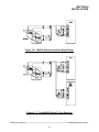
Figure 8.5 – Typical Interrupt Wiring
Figure 8.6 – Typical Analog I/O Wiring
Figure 8.7 – Typical Fault Interlock Wiring
Figure 8.8 – Typical Network Wiring
Figure 8.9 – Alternative Serial Connector Wiring
Figure 8.10 – M4500 Resolver Interface (stand alone)
Figure 8.11 – Two M4500’s Slaved to One Resolver
53
54
54
56
58
59
60
62
62
65
65
M4500 User’s Manual
SYSTEMS Electronics Group
- iii -
CONTENTS
APPENDICES
I/O Board Data Sheets
Appendix A
S4516 Serial Communications Board
S4563 16 Point 10-30VDC Input (sourcing)
S4568 8-Input/8-Output 10-30VDC I/O (sourcing)
S4573 16 Point 10-30VDC Output (sourcing)
A1
A7
A11
A17
RS-232 Pinouts/Cables
Appendix B
Field Wiring Connector Pinouts
Appendix C
M4500 User’s Manual
SYSTEMS Electronics Group
- iv -
SECTION 1
GENERAL DESCRIPTION
The M4500 Product Line (generically referred to as the M4500) is a modular design consisting of a
series of high performance PLC (Programmable Logic Controller) chassis with a fully integrated
PLS (Programmable Limit Switch), digital I/O boards, serial communication board,
display/keypads, and power supply. Eight versions are available:
M4500:
M4501:
M4502:
M4503:
M4508:
M4509:
M4512:
M4513:
4 I/O SLOT PLC/PLS
4 I/O SLOT PLC ONLY
3 I/O SLOT PLC ONLY WITH DISPLAY/KEYPAD
3 I/O SLOT PLC/PLS WITH DISPLAY/KEYPAD
8 I/O SLOT PLC/PLS
8 I/O SLOT PLC ONLY
12 I/O SLOT PLC/PLS
12 I/O SLOT PLC ONLY
The M450X part numbers consist of the chassis with processor, resolver interface (M4500, M4503,
M4512 and M4508) and either 3 I/O slots (M4502 and M4503), 4 I/O slots (M4500 and M4501), 8
I/O slots (M4508 and M4509) or 12 I/O slots (M4512 and M4513). I/O boards (16 and 32 point
Input and 16 point Output) are installed by the user in the I/O slots based on the requirements of the
application. The optional D4590 2 Line X 20 character or D4591 2 Line X 40 character displays
with 24 key (3 Row X 8 Column) keypads are available for use as a general operator interface or for
PLS timing channel programming (the D4591 Display/Keypad is built into the M4502 and M4503).
The Serial Communication board is available for communications with other S3000/M4000
products or with other manufactures PLC or host computers.
A typical M4500 system consists of the PLC Processor/Chassis (M4500-M4509), Power Supply
(P4500), digital I/O boards (S45XX) as required, Serial Communications boards (S4516) as
required, and optional Display/Keypad (D4590 or D4591). The M4502 and M4503 contain a builtin power supply and the D4591 Display/Keypad.
________________________________________________________________________________
1.1 PLC SECTION
The PLC section of the M4500 is a high performance programmable logic controller which
incorporates a built-in processor, user program memory, user data memory, RS-232 programming
port, interface to the Display/Keypad, and interface to the I/O slots motherboard. The scan time of
the PLC section is on the order of 0.25 milliseconds per K with scan times as low as 80
microseconds for short programs. Two additional interrupt inputs allow through-puts even less than
80 microseconds. Program memory consists of 32K bytes of battery-backed CMOS RAM memory.
Data memory consists of 8K bytes RAM memory.
M4500 User’s Manual
SYSTEMS Electronics Group
-1-
SECTION 1
GENERAL DESCRIPTION
The PLC section supports addressing of up to 12 I/O slots.
Note: Geographical addressing is not used. The slot addresses are specified by dip switches on the
I/O board themselves. The PLC section is capable of addressing up to 64 bytes at each slot.
Memory mapped I/O is incorporated to provide the greatest degree of flexibility in accessing the
I/O boards.
Programming of the PLC section is implemented with SYSdev, an IBM PC or compatible software
package that allows the user to create, document, and compile the user logic program as well as
directly interface to the M4500 for program down-load and on-line monitoring. Complete program
printouts including the user program listing, cross reference, and memory map can also be
generated.
________________________________________________________________________________
1.2 PLS SECTION
The PLS section is a high speed programmable limit or cam switch which accepts angular position
information in the form of resolver format signals and converts these to digital. The M4500 is
configurable for 8, 16, 32 or 64 timing channels. These are mapped to internal memory locations of
the M4500 for use by the PLC section or can be written to output boards for use in general PLS
applications. The timing channels can be programmed "on" and "off" at user defined position setpoints. Each timing channel can be programmed with up to 50 unique "on-off" set-points or with a
pulse train of fixed "on" and "off" divisions throughout the entire channel.
The scale factor of the PLS is programmable from 2 to 4096 divisions per revolution while the
offset is programmable from 0 to one minus the scale factor. The PLS supports up to 8 PLS
programs when 8 timing channels are used and the scale factor is less than 512 (less PLS programs
when more channels are used or the scale factor is greater than 512). A typical application of using
multiple PLS programs would be in stamping press applications where different die sets would be
used for different stampings. The timing signals for each die set (up to 8 different die sets) would be
programmed and saved in a specific PLS program and then as the different die sets were used, the
specific PLS program would be called up and used for that die set, saving the operator from having
to re-program all the timing signals every time that die set was used.
Speed Compensation is available for timing channels 0 through 7. This is used to compensate for
the mechanical response time of a device activated by a particular timing channel. The speed
compensation algorithm "leads" the desired activation position by a time in milliseconds entered for
that channel. Thus as the speed increases, the point at which the device is activated is advanced to
compensate for the response time of the device.
Note: The compensation parameter is entered in milliseconds, not degrees per RPM, which
simplifies set-up since the time that is be compensated for is in milliseconds.
M4500 User’s Manual
SYSTEMS Electronics Group
-2-
SECTION 1
GENERAL DESCRIPTION
The M4500 is generally interfaced with the RSV34-MS1 resolver as the position transducer,
however, virtually any type of resolver which incorporates a rotor reference signal and two stator
feedback signals can be used.
________________________________________________________________________________
1.3 INTERRUPT INPUTS
The M4500 modules contain two 10-30VDC differential interrupt inputs. The inputs are 10-30VDC
differential inputs which can be enabled as interrupt inputs or disabled and used as standard inputs.
When enabled as interrupts, an "off" to "on" transition of the enabled input activates an interrupt
call to a user programmed file (ufunc00 for input0 and ufunc01 for input1). This suspends the main
program file until the interrupt file execution is completed, at which time program execution
resumes at the place in the main file where the interrupt occurs. This mechanism allows ultra fast
through-puts to be implemented if required.
The interrupt inputs are true differential inputs which can be wired as either sinking (true low) or
sourcing (true high) depending on the device used to drive the input. Individual LED status
indication is provided for each input.
________________________________________________________________________________
1.4 ANALOG I/O
Two analog inputs and two analog outputs are built into the M4500. The analog inputs are 0-5 volt
which can also be used as 0-20ma and 0-10 volt inputs when external resistors are installed to
perform the respective conversion (250ohm for 0-20ma, two resistors as a voltage divider for 010VDC). The analog outputs are 0-10 volt which can also be used to drive 0-5 volt inputs using a
similar external resistor conversion.
The analog inputs are of 10 bit resolution (0-1023) incorporating high speed conversion (less than
25 microsecond) and are updated once every other main scan. The analog outputs are of 8 bit
resolution (0-255) and are updated every main scan.
M4500 User’s Manual
SYSTEMS Electronics Group
-3-
SECTION 1
GENERAL DESCRIPTION
________________________________________________________________________________
1.5 DISPLAY/KEYPAD
Two Display/Keypads are available for the M4500: the D4590 which incorporates a 2 line X 20
character display and the D4591 which incorporates a 2 line X 40 character display. Both displays
incorporate a 24 key keypad which is arranged in 3 rows by 8 columns. Back-lighted LCD
technology at 0.19" character height provides both high visibility in low light conditions and high
character density.
To minimize space utilization, the keypad/display can be mounted to the back of the M4500 in
cases where the M4500 would be door mounted. The D4590 is designed to mount to the back of the
M4500/M4501 while the D4591 is designed to mount to the back of the M4508/M4509.
Note: If the display is not mounted to the back of the module, either display can be used with either
module. The Display is equipped with a gasket and is fully sealed to prevent the ingress of
contaminates to the display or M4500.
The displays can be used as a general purpose operator interface or can be used to implement the
PLS programming commands. When used as a general purpose interface, complete control of the
display is provided through commands accessed through the user program in the PLC section.
Commands such as: "position cursor", "clear display", "enter characters into display", "blink
character", as well as an ASCII string conversion system function allow easy and complete control
of the display directly in the M4500 user's program. The PLS program commands are resident in the
firmware of the M4500 and can either be enabled or disabled in the user's program.
The keypads are 3 row by 8 column sealed keypads which can either be used as a general purpose
operator interface or to implement the PLS programming commands. Key depressed decode is
performed automatically by the M4500 with the key number depressed mapped directly to an
internal memory location of the M4500. The keypad overlay itself simply contains clear windows
over the keys. Customization of the keypad is performed by placing a placard behind the overlay
(between the overlay and the keys) with the desired key legends. The keys on the D4590
display/keypad are spaced at 0.5" while the keys on the D4591 are spaced at 0.75" spacing.
The D4591 Display/Keypad is built directly into the M4502 and M4503 modules.
M4500 User’s Manual
SYSTEMS Electronics Group
-4-
SECTION 1
GENERAL DESCRIPTION
________________________________________________________________________________
1.6 SERIAL COMMUNICATIONS BOARD
Serial communications to other equipment is implemented with the S4516 Serial Communications
board. The S4516 contains one S3000 serial network interface port and one RS-232/RS-422 User
port. Multiple S4516 boards can be installed in one M4500 (up to the number of slots for that
particular model) to allow the use of multiple S3000 network ports or RS-232/RS-422 User ports.
SERIAL NETWORK PORT: The serial network port conforms to the S3000-N1 network
protocol. This network is a high speed (up to 344KBPS), twisted pair, serial network configured in
a master/slave topology. Up to 32 M4500, S3000, or M4000 modules/processors (nodes) can be
connected on one network. Communications between the nodes on the network is controlled via
commands (sfunc13) in the user application program resident in the node acting as the master.
USER PORT: This port is available as a general purpose RS-232/RS-422 port accessed under
software control of the user program. Typical uses of this port are connection to other control
equipment, data acquisition to a host PLC, etc.. Drivers are available for this port that implement
the MODBUS protocol and the Allen-Bradley DF1 protocol.
________________________________________________________________________________
1.7 DIGITAL I/O BOARDS
Digital I/O boards are added to the M4500 by the user as required by the application. All I/O boards
incorporate removable field wiring arms for ease of replacement. I/O slot addressing is
implemented via dip switches on the I/O boards. Any mix of I/O boards can be installed in an
M4500 (all input boards, all output boards, inputs and outputs, etc.).
________________________________________________________________________________
1.8 DIAGNOSTICS/FAULT DETECTION
The M4500 contains comprehensive fault detection routines which verify the proper operation of
the module at all times. Each detected fault has a corresponding fault code which can be viewed
using SYSdev, providing a description of the fault and recommended corrective action. In addition,
the M4500 contains a fault interlock output (24VDC, 500mAMP, sinking) which can be interlocked
to the control system for system shut down or annunciation when a fault is detected. In addition to
the fault detection, a hardware confidence test is resident in the module to provide a complete test
of the internal module hardware. This test is initiated through SYSdev and can be used to verify the
M4500 for proper operation.
M4500 User’s Manual
SYSTEMS Electronics Group
-5-
SECTION 1
GENERAL DESCRIPTION
________________________________________________________________________________
1.9 LED STATUS INDICATIONS
The following three status LED's are located on the front M4500: PWR, RUN, and FLT. The
definitions of these LED's are as follows:
PWR: "On" when +5VDC power is applied to the M4500.
RUN: "On" steady when the M4500 is running a valid user's application program. "Off" when an
internal fault is detected or when a valid user's program has not been loaded. The RUN led is
flashed during program download and also when the hardware confidence test is executed.
FLT: "On" when an internally detected fault has occurred in the M4500. See section 6 for more
details on the fault routines and error codes.
M4500 User’s Manual
SYSTEMS Electronics Group
-6-
SECTION 2
PLC FEATURES
________________________________________________________________________________
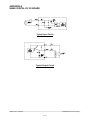
2.1 PLC PROGRAM STRUCTURE
The PLC section of the M4500 is programmed with SYSdev. The SYSdev programming language
is a combination of Ladder, High-level (subset of C) and Assembly (MCS-96). All the files which
comprise a SYSdev program are programmed in the same language format. Each file can be written
in any combination of the language types. The typical M4500 PLC program consists of the
following files:
1) Initialization file (optional): executed once at power up.
POWER-UP
2) Main Program file (required): scanned continuously.
3) Timed Interrupt file (optional): executed once every 0.250
to 65.000 milliseconds as set by the user.
4) User Function file (optional): up to 100 user defined
subroutines which can be called from any of the above
files.
5) Input Interrupts (optional): the two input interrupts can be
enabled or disabled independently. When the interrupts
are enabled, Input0 interrupt calls ufunc00 when activated
("off" to "on" transition of input0) while input1 interrupt
calls ufunc01.
INIT
FILE
TIMED
INTERRUPT
MAIN
PROG
FILE
UFUNC
Note: ufunc00 must be created by the user if the input0
interrupt is enabled and ufunc01 if the input1 interrupt is
enabled.
Each file is executed sequentially from beginning to end. The main program file is executed
(scanned) continuously unless interrupted by the timed interrupt or either of the input interrupts.
When this occurs, main program execution is suspended while the interrupt file is executed. At the
completion of the interrupt, program execution resumes at the point in the main program where the
interrupt occurred.
Each file is implemented as a series of consecutive blocks. Each block is defined as one of the three
programming languages: Ladder, High-level or Assembly. Blocks of the different languages can be
intermixed as necessary within the file.
Since the M4500 incorporates memory mapped I/O, I/O update is performed by the user's
application program. In most applications this is done at the beginning of the main program and/or
the beginning of the timed interrupt.
See the M4500 Program Development Manual for complete details on programming the PLC
section of the M4500.
M4500 User’s Manual
SYSTEMS Electronics Group
-7-
SECTION 2
PLC FEATURES
________________________________________________________________________________
2.2 SPECIAL FUNCTION VARIABLES (SFV's) (Directly addressed)
Many of the features of the M4500 are accessed via certain variables in the M4500. These are
referred to as "Special Function Variables". The following is the list of SFV's of the M4500 and is
provided as a reference only. For a complete description of each SFV, refer to the M4500 Program
Development Manual.
Address
Description
B160
B160.0
B160.1
thru
B160.5
B160.6
B160.7
PLS Command Flags:
Execute PLS command (from PLC)
Reserved (Do not access)
B161
B161.0
B161.1
B161.2
B161.3
B161.4
B161.5
B161.6
B161.7
System Enable Flags:
PLS Mode Enable
PLS CH0-7 Speed Compensation Enable
PLS Keypad Commands Enable
Analog I/O Update Enable
PLS Update in TIMED(1)/ PLS Update in MAIN(0)
PLS Program Commands Enable
sfunc13 slave mode enable in S4516
sfunc18 interleaved(0)/ executed complete(1)
W162
W164
B166
B167
AIN0 - Analog Input 0 (0-1023)
AIN1 - Analog Input 1 (0-1023)
AOUT0 - Analog Output 0 (0-255)
AOUT1 - Analog Output 1 (0-255)
B170
B171
B172
B173
B174
B175
B176
B177
CH0 PLS Channel byte 0 (CH00-07)
CH1 PLS Channel byte 1 (CH10-17)
CH2 PLS Channel byte 2 (CH20-27)
CH3 PLS Channel byte 3 (CH30-37)
CH4 PLS Channel byte 4 (CH40-47)
CH5 PLS Channel byte 5 (CH50-57)
CH6 PLS Channel byte 6 (CH60-67)
CH7 PLS Channel byte 7 (CH70-77)
Reserved (Do not access)
Bypass "Recall" Ack
Reserved (Do not access)
M4500 User’s Manual
SYSTEMS Electronics Group
-8-
SECTION 2
PLC FEATURES
Address
Description
W178
W180
W182
W184
W186
W188
W192
Resolver Position (updated in TIMED Interrupt)
Resolver Position (updated in MAIN Program)
Resolver RPM
Resolver Period (msec per revolution)
Resolver Scale Factor
Resolver Offset
Resolver Period (speed compensation)
B191
B194
B8158
Depressed Key on Keypad (0=no key, 1-24=key)
Display wait delay (B194=28 for D4590, B194=47 for D4591)
Keypad Debounce time (in main scans)
W8154
W8156
B8159
Slave Slot Address for S4516 sfunc13 slave mode
S4516 Slot Address for sfunc10/11/13
Current Firmware Revision
PLS Programming (from PLC) SFV's:
B190
Selected PLS Channel Program (0-7)
B212
PLS Command:
B212=09: Recall Channel
B212=27: Single set-point programming command
B212=43: Pulse Train Programming command
For Recall Channel command:
B213
Channel to read (set by user prior to command)
B213
Recall State (0="off", 1="on") (return value)
W214
Position of set-point change of state (return value)
For Single set-point command:
B213
Channel to program set-point
W214
"ON" setpoint (in degrees)
W216
"OFF" setpoint (in degrees)
B218
Program state (0="off", 1="on")
For Pulse Train command:
B213
Channel to program set-point
W214
"START" position (in degrees)
B216
"ON" Duration
B217
"OFF" Duration
M4500 User’s Manual
SYSTEMS Electronics Group
-9-
SECTION 2
PLC FEATURES
________________________________________________________________________________
2.3 SPECIAL FUNCTION VARIABLES (SFV's) (Indirectly addressed)
Address
Description
2100H
2126H
2127H
2128H
2129H
212aH
212bH
212cH
212dH
2200H-2207H
2208H-220fH
2210H-2217H
2218H-221fH
2220H-2227H
2228H-222fH
2230H-2237H
2238H-223fH
Number of PLS Channels (8,16,32,64)
CH0 Speed Compensation (active)
CH1 Speed Compensation (active)
CH2 Speed Compensation (active)
CH3 Speed Compensation (active)
CH4 Speed Compensation (active)
CH5 Speed Compensation (active)
CH6 Speed Compensation (active)
CH7 Speed Compensation (active)
Speed Compensation array (PLS program=0)
Speed Compensation array (PLS program=1)
Speed Compensation array (PLS program=2)
Speed Compensation array (PLS program=3)
Speed Compensation array (PLS program=4)
Speed Compensation array (PLS program=5)
Speed Compensation array (PLS program=6)
Speed Compensation array (PLS program=7)
M4500 User’s Manual
SYSTEMS Electronics Group
- 10 -
SECTION 2
PLC FEATURES
________________________________________________________________________________
2.4 MEMORY MAPPED I/O
X and Y variables are not supported in the M4500. Instead the I/O slots of the chassis are mapped
into the memory space of the M4500, accessed as Byte(B) variables. The addresses of the different
slots are assigned as follows:
Group-Slot
Byte
0-0
0
1
2
3
B7424
B7425
B7426
B7427
0-1
0
1
2
3
B7488
B7489
B7490
B7491
0-2
0
1
2
3
B7552
B7553
B7554
B7555
0-3
0
1
2
3
B7616
B7617
B7618
B7619
1-0
0
1
2
3
B7680
B7681
B7682
B7683
1-1
0
1
2
3
B7744
B7745
B7746
B7747
1-2
0
1
2
3
B7808
B7809
B7810
B7811
1-3
0
1
2
3
B7872
B7873
B7874
B7875
Address
M4500 User’s Manual
SYSTEMS Electronics Group
- 11 -
SECTION 2
PLC FEATURES
Unlike the S3000 and M4000, the M4500 does not automatically perform the I/O update at the
beginning of the program. The I/O update on the M4500 is performed by the user's program.
Internal Byte(B) variables serve as the I/O image. Input boards are read and stored in the input
image (B) bytes while output image (B) bytes are used to store the value of the outputs and then are
written to the outputs. See the M4500 Program Development Manual for more details.
M4500 User’s Manual
SYSTEMS Electronics Group
- 12 -
SECTION 3
PLS FEATURES
________________________________________________________________________________
3.1 STANDARD PLS FEATURES
The following are the standard PLS features built into the M4500 firmware. These features are
available independent of the user's PLC application program.
________________________________________________________________________________
3.1.1 TIMING CHANNELS
The M4500 is configurable for 8, 16, 32 or 64 timing channels. These are mapped to internal
memory locations of the M4500 for use by the PLC section or can be written to output boards for
use in general PLS applications. The timing channels can be programmed "on" and "off" at user
defined position set-points. Each timing channel can be programmed with up to 50 unique "on-off"
set-points or with a pulse train of fixed "on" and "off" divisions throughout the entire channel.
The number of timing channels used (8, 16, 32, or 64) is predicated by the application. On
applications requiring a large number of channels, up to 64 are available. On applications requiring
only a small number of channels, as few as 8 are available. The more channels used, the higher the
over-head scan time will be to implement the timing channels. Therefore, it is advantageous to
configure the M4500 for no more than the number of channels that are required.
________________________________________________________________________________
3.1.2 SCALE FACTOR
The scale factor of the PLS is programmable from 2 to 4096 divisions per revolution. If 360 degrees
are to be used, set the scale factor to 360.
________________________________________________________________________________
3.1.3 OFFSET (ELECTRONIC ZERO)
The offset is used to electronically zero the resolver shaft. The M4500 contains an auto zero
algorithm which will automatically calculate the offset required to make the current position of the
resolver shaft zero. This is implemented by simply entering "0" for the offset. This indicates to the
M4500 to auto zero the offset. In addition, the user can actual enter the desired position that is to be
zero. This allows the offset to be set in any way desired.
M4500 User’s Manual
SYSTEMS Electronics Group
- 13 -
SECTION 3
PLS FEATURES
________________________________________________________________________________
3.1.4 PLS PROGRAMS
The PLS supports up to 8 PLS programs. A typical application of using multiple PLS programs
would be in stamping press applications where different die sets would be used for different
stampings. The timing signals for each die set (up to 8 different die sets) would be programmed and
saved in a specific PLS program and then as the different die sets were used, the specific PLS
program would be called up and used for that die set, saving the operator from having to re-program
all the timing signals every time that die set was used.
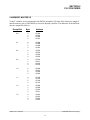
The number of PLS programs which can be used is a function of the number of channels used and
the scale factor used. The matrix below outlines how many PLS programs are available as a
function of the scale factor and number of channels. The numbers in the matrix are the number of
PLS programs available. An "*" indicates an invalid scale factor/number of channels combination.
Scale Factor
0 - 511
512 - 1023
1024 - 2047
2048 - 4096
8
8
4
2
1
Number of Channels
16
32
4
2
2
1
1
*
*
*
64
1
*
*
*
________________________________________________________________________________
3.1.5 SPEED COMPENSATION
Speed Compensation is available for timing channels 0 through 7. This is used to compensate for
the mechanical response time of a device activated by a particular timing channel. The speed
compensation algorithm causes the timing channel to "lead" the programmed timing set-point for
that channel by a time in milliseconds entered for that channel. Thus as the speed increases, the
point at which the device is activated is advanced to compensate for the response time of the device.
Note: The compensation parameter is entered in milliseconds, not degrees per RPM, which
simplifies set-up since the time that is be compensated for is in milliseconds.
The speed compensation feature is enabled with bit 1 in the System Enable Byte (B161). When
enabled, the speed compensation for channels 00 through 07 can all be set independently to any
value between 0 and 255 milliseconds. If speed compensation for a particular channel is not to be
used, set the compensation value to "0".
M4500 User’s Manual
SYSTEMS Electronics Group
- 14 -
SECTION 3
PLS FEATURES
________________________________________________________________________________
3.2 ADVANCED PLS FEATURES
The PLS is fully integrated with the PLC. What this means is that the actual resolver position,
current RPM, and every other PLS parameter can be accessed by the PLC section. The PLC can
even execute the PLS programming commands that would normally be executed through SYSdev
or the D4590/91 Display/Keypad. This allows virtually any PLS feature that can be dreamed of to
be implemented. Examples of this are:
Brake Wear Compensation: The brake wear compensation algorithm is used in conjunction
with presses which incorporate a top dead center (TDC) or back dead center (BDC) stop. With these
presses, a timing signal is used to de-clutch the press for TDC or BDC stops. However, as the brake
wears, the press will no longer stop at TDC but will instead overshoot. The brake wear
compensation algorithm automatically adjusts the TDC timing such that the press always stops at
the desired stopping position regardless of brake wear.
Brake Wear Alarm: In conjunction with the brake wear compensation, brake response
determination and a brake wear alarm can be implemented in the PLC section. This determines the
actual number of degrees the brake takes to stop the press (from de-clutch to stop). The brake wear
alarm can be activated if the brake response exceeds a preset number of degrees.
Speed Windows: These signals can be activated at preset speed thresholds as desired or needed.
Since the RPM is directly available to the PLC section, virtually an unlimited number of speed
windows could be generated by the PLC section.
Automatic Zero: Since the offset of the PLS can be accessed by the PLC section, it can also be
changed in response to any desired logic condition, even as a function of speed which would, in
affect, implement a speed compensation for all the timing channels.
The above advanced PLS features are not implemented in the firmware of the M4500 but would be
instead implemented with user logic in the PLC section of the M4500.
M4500 User’s Manual
SYSTEMS Electronics Group
- 15 -
SECTION 3
PLS FEATURES
________________________________________________________________________________
3.3 PLS CHANNEL PROGRAMMING
The PLS section of the M4500 is programmed either through SYSdev using an IBM PC or
Compatible or through the PLS commands of the D4590 or D4591 Display/Keypad. When using
SYSdev, the PLS section can either be configured and the timing signals programmed off-line and
then down-loaded to the M4500 or the PLS timing channels can be programmed on-line, while the
M4500 is in operation. The IBM PC or compatible is interfaced to the PLS section of the M4500
via the "PROG" port of the M4500 using an RS-232 cable from the COM port on the computer. The
following PLS programming commands are available when using SYSdev or the D4590/91
Display/Keypad:
PLS Configuration including:
Scale Factor (2-4096)
Offset
Selected PLS Program (0-7)
Number of Timing Channels (8,16,32,or 64)
Timing Channel Speed Compensation (Channels 00 thru 07)
On and Off-line timing channel programming including:
single set-point programming
pulse train channel programming
timing channel fine tune (SYSdev only)
Channel set-points download to M4500 (SYSdev only)
Channel set-points upload from M4500 (SYSdev only)
Configuration and channel set-points print-outs (SYSdev only)
See section 4 for details on programming the PLS section using the keypad/display. See section 5
for details on programming the PLS section using SYSdev.
M4500 User’s Manual
SYSTEMS Electronics Group
- 16 -
SECTION 3
PLS FEATURES
________________________________________________________________________________
3.4 IMPLEMENTING M4500 AS A STAND-ALONE PLS
The M4500 is fundamentally a PLC with built-in PLS features. The M4500 can be used as a standalone PLS (PLC section not used) by downloading the program "BASICPLS" to the M4500. This is
a PLC program which simply enables all the PLS features and maps the timing channels to the
following outputs:
CH00-07
CH10-17
CH20-27
CH30-37
CH40-47
CH50-57
CH60-67
CH70-77
OUTPUT SLOT0-0: BYTE0
OUTPUT SLOT0-0: BYTE1
OUTPUT SLOT0-1: BYTE0
OUTPUT SLOT0-1: BYTE1
OUTPUT SLOT0-2: BYTE0
OUTPUT SLOT0-2: BYTE1
OUTPUT SLOT0-3: BYTE0
OUTPUT SLOT0-3: BYTE1
The "BASICPLS" program is included with the SYSdev software package and is loaded into the
"EXAMPLES" sub-directory of the "PLS51" sub-directory. To download "BASICPLS" into the
M4500, perform the following:
1) Power up the M4500 and the IBM PC or compatible loaded with SYSdev.
2) Connect an RS-232 cable from the computer COM port to the "PROG" port on the M4500.
3) From the root directory of the hard drive that SYSdev is loaded on, type:
SYSDEV \PLS51\EXAMPLES BASICPLS<ENTER>.
4) From the main development menu of SYSdev, select "6: Target Board Interface".
5) Download the "BASICPLS" application program to the M4500 by selecting "1: Download Program to
Target Board" from the target board interface menu. A prompt will be displayed verifying the
download, press the <ENTER> key to start the download. Once the download is complete, press
any key to return to the target board interface menu.
6) Return to the SYSdev main menu and then exit SYSdev.
When loaded with "BASICPLS", the M4500 will simply perform as a programmable limit switch.
The timing channels can be programmed with either SYSdev or through the keypad of the
D4590/91. All PLS features are enabled including speed compensation, etc.
M4500 User’s Manual
SYSTEMS Electronics Group
- 17 -
SECTION 3
PLS FEATURES
(This Page Intentionally Left Blank)
M4500 User’s Manual
SYSTEMS Electronics Group
- 18 -
SECTION 4
PLS PROGRAMMING
USING THE KEYPAD/DISPLAY
The D4590 and D4591 are keypad/displays that can be used as general purpose operator interfaces
as well as PLS programmers for the M4500. The PLS programming commands and menu displays
are built-in into the firmware of the M4500 and active when the display is not used as a general
purpose operator interface. When used as a PLS programmer, the keypad/displays are used to
configure and program the timing channels of the M4500. The keypad/displays incorporate a built
in 2 line by 20 or 40 character alphanumeric display which displays command prompts, set-point
data, configuration data, as well as the resolver position or speed (RPM) in real-time. Of the 24
keys of the keypad, 18 of the keys are used to select the PLS programming commands and enter
data.
________________________________________________________________________________
4.1 CHANNEL SET-POINT PROGRAMMING COMMANDS
Three channel set-point programming commands are available with the keypad/displays: single setpoint programming, pulse train programming, and clear channel. The single set-point command is
used to enter a unique "on" set-point in a channel. This command programs the channel "on" from a
user specified "on" position to a user specified "off" position. The pulse train command is used to
program a channel with set-points of a fixed "on" and "off" duration through-out the entire channel.
The clear channel command is used to clear all set-points from the currently selected channel.
________________________________________________________________________________
4.2 PLS CONFIGURATION PARAMETERS
In addition to channel programming, the keypad/displays are used to set the M4500 PLS
configuration. This includes setting the PLS scale factor and offset, select the PLS program, and set
the speed compensation for channels 00 through 07.
M4500 User’s Manual
SYSTEMS Electronics Group
- 19 -
SECTION 4
PLS PROGRAMMING
USING THE KEYPAD/DISPLAY
________________________________________________________________________________
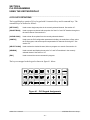
4.3 PLS KEY DEFINITIONS
The keypad/displays contain a 24 key keypad with 10 numerical keys and 6 command keys. The
command keys are defined as follows:
[SET POINT]
Used to enter single set-points in the currently selected channel. See section 4.7.
[PULSE TRAIN]
Used to program a channel with set-points of a fixed "on" and "off" duration through-out
the entire channel. See section 4.8.
[CLEAR CHAN]
Used to clear all set-points from the currently selected channel.
[CONFIG]
Used to set the PLS configuration parameters including: the scale factor, offset, select
the PLS program, and set the speed compensation for channels 00 through 07. See
section 4.5.
[SELECT CHAN]
Used to select the desired channel, either to program or to search. See section 4.6.
[SEARCH]
Used to search and display the set-point "on" and "off" transitions in the currently
selected channel. See section 4.10.
[ESC]
Used to cancel the current command in progress
The keys are mapped to the keypad as shown in figure 4.1 below:
Figure 4.1 - PLS Keypad Assignments
M4500 User’s Manual
SYSTEMS Electronics Group
- 20 -
SECTION 4
PLS PROGRAMMING
USING THE KEYPAD/DISPLAY
________________________________________________________________________________
4.4 PLS DISPLAY FIELDS
The keypad/displays contain either a 2 line by 20 character (D4590) or 2 line by 40 character backlighted LCD display which normally displays a default channel message or various prompts while
commands are entered. The format of the default channel message is:
CH:xx SETPT:yyy []
RPM:0000 POS:888
1) "xx" is the currently selected channel in octal .
2) "yyy" is the position where the set-point transition is located.
3) The [] after the set-point position is the channel status indicator.
a) If the channel status indicator is a solid block "[]", the set-point transitions "on" at the displayed
position.
b) If the channel status indicator is blank, the set-point transitions "off" at the displayed position.
c) If the channel is programmed either all "on" or all "off", the position will read "---" and the channel
state indicator will be set "on" or "off" as appropriate.
________________________________________________________________________________
4.5 SETTING THE PLS CONFIGURATION
The following PLS configuration parameters can be set via the keypad/display [CONFIG]
command: PLS program, scale factor, offset, and CH00 through CH07 speed compensation.
Note: Once the [CONFIG] command is initiated, each parameter will be prompted for and
displayed sequentially by the keypad/display. To simply view the existing configuration parameters
without changing them, press [ENTER] when the corresponding parameter is displayed. The
[CONFIG] command can be exited at any time simply by pressing the [ESC] key.
The following configuration parameters are prompted for sequentially:
1)
2)
3)
4)
5)
6)
7)
8)
9)
10)
11)
12)
PLS Program (0-7)
Offset (0 to Scale Factor-1)
Scale Factor (2-4096)
Number of Timing Channels (8,16,32,or 64)
CH00 Speed Compensation (0 to 255msec)
CH01 Speed Compensation (0 to 255msec)
CH02 Speed Compensation (0 to 255msec)
CH03 Speed Compensation (0 to 255msec)
CH04 Speed Compensation (0 to 255msec)
CH05 Speed Compensation (0 to 255msec)
CH06 Speed Compensation (0 to 255msec)
CH07 Speed Compensation (0 to 255msec)
M4500 User’s Manual
SYSTEMS Electronics Group
- 21 -
SECTION 4
PLS PROGRAMMING
USING THE KEYPAD/DISPLAY
To view or set the configuration parameters, perform the following:
1) Press the [CONFIG] key to initiate the configuration command.
2) The display will now read "PLS PROGRAM:x" where x is the currently selected PLS program. To select
a new PLS program, enter a number between 0 and 7 and press [ENTER]. The timing set-points for the
selected PLS program will be recalled from memory and used as the active set-points for the timing
signals. If the PLS program is not to be changed, simply press [ENTER].
3) Now the display will read "OFFSET:xxxx" where xxxx is current offset. This offset is used primarily to
electronically zero the resolver shaft at machine zero. The offset can be programmed from 0 to one
minus the scale factor. To set the offset, perform the following: Locate the machine at machine zero.
Read the resolver shaft position on the keypad/display. Enter the value read and press [ENTER]. The
M4500 will calculate the value required to make the position entered machine zero and enter this as the
offset (this value may not equal the value entered).
Alternatively, the resolver can be zeroed simply enter the number 0 and pressing [ENTER]. The M4500
PLS contains an auto zero algorithm which will calculate the offset required to make the current position
zero.
To continue without changing the offset, simply press [ENTER].
4) Next the display will read "SCALE FACTOR:xxxx" where xxxx is the current scale factor. The scale
factor of the M4500 PLS is programmable from 2 to 4096 divisions per revolution. For 360 degrees per
revolution, the scale factor should be set to 360. To change the scale factor, enter the new scale factor
and press [ENTER]. To continue without changing the scale factor simply press [ENTER].
CAUTION!!
Changing the scale factor after timing channels have been previously
programmed will result in invalid set-points. It is recommended that all timing
channels be re-programmed after setting the scale factor.
5) The display will now read "NUMBER CHANNELS:xx" where xx is the currently specified number of
channels. The M4500 PLS supports either 8, 16, 32 or 64 timing channels. Enter the number of channels
to be used (8, 16, 32, or 64) and press [ENTER]. If the number of channels are not to be changed,
simply press [ENTER] to continue.
6) The last set of configuration parameters that will be prompted for are the speed compensation presets
for channels 00 through 07. Each of these channels can be programmed to have from 0 to 255
milliseconds of timing signal "lead" (see section 3.1.5). The values entered for the speed compensation
are in milliseconds. This is the amount of time that the timing signal will lead the programmed timing setpoint as the speed of the machine is varied. The speed compensation for each channel is independently
set.
The display will prompt "CHxx SPEED COMP:yyy" where xx is the channel (00 to 07) and yyy is the
currently programmed speed compensation (in milliseconds) for that channel. To change the
compensation value, enter the new number (from 0 to 255) and press [ENTER]. The compensation for
the next channel will then displayed. If speed compensation for a particular channel is not to be used,
enter "0" for the compensation for that channel. If the compensation value for a particular channel is not
to be changed, simply press [ENTER] to continue.
M4500 User’s Manual
SYSTEMS Electronics Group
- 22 -
SECTION 4
PLS PROGRAMMING
USING THE KEYPAD/DISPLAY
7) The [CONFIG] command is now complete, the display will return to showing the last channel and setpoint selected.
________________________________________________________________________________
4.6 SELECTING A NEW CHANNEL NUMBER
To select a new channel number, either to search for set-points or to program, perform the
following:
1) Press the [SELECT CHAN] key.
2) The display will prompt "ENTER CHAN:_". Enter the new channel, in octal, and press the [ENTER] key.
Note: Valid channel numbers are 00 thru 07, 10 thru 17, 20 thru 27, 30 thru 37, etc..
Example #1: The following example sets the working channel to 01:
Key Depressed
Display
[SELECT CHAN]
[1]
[ENTER]
ENTER CHAN:_
ENTER CHAN:1_
CH:01 SETPT:xxx []
________________________________________________________________________________
4.7 SINGLE [SET-POINT] PROGRAMMING COMMAND
The single set-point command is used to enter a unique "on" set-point in the currently selected
channel. This command programs the channel "on" from a user specified "on" position to a user
specified "off" position.
Note: Programming a new set-point in a channel does not clear out any previous set-points. This
allows multiple set-points to be programmed in a channel. If a channel is to be "moved", the
channel must first be cleared and then re-programmed using the [SET-POINT] command.
To program a single set-point, perform the following:
1) Press the [SET-POINT] key to initiate the single set-point programming command.
2) The display will prompt ""ON" SETPT:_". Enter the position the set-point is to turn "on" and press
[ENTER].
3) The display will now prompt ""OFF" SETPT:_". Enter the position the set-point is to turn "off" and press
[ENTER].
4) The M4500 PLS will now program the channel "on" from the entered "on" position to the entered "off"
position.
Note: Any number of unique set-points may be entered in a selected channel. In addition, the entire
channel can be programmed "on" simply by specifying the "on" and "off" prompts with the same position.
M4500 User’s Manual
SYSTEMS Electronics Group
- 23 -
SECTION 4
PLS PROGRAMMING
USING THE KEYPAD/DISPLAY
M4500 User’s Manual
SYSTEMS Electronics Group
- 24 -
SECTION 4
PLS PROGRAMMING
USING THE KEYPAD/DISPLAY
Example #1: The following key sequence programs the currently selected channel "on" from 20 degrees to
40 degrees:
Key Depressed
Display
[SET-POINT]
[2]
[0]
[ENTER]
[4]
[0]
[ENTER]
"ON" SETPT:_ []
"ON" SETPT:2_ []
"ON" SETPT:20_ []
"OFF" SETPT:_
"OFF" SETPT:4_
"OFF" SETPT:40_
CH:xx SETPT:020 []
Example #2: This example programs the selected channel entirely "on" by entering 000 for both the "on" and
"off" prompts:
Key Depressed
Display
[SET-POINT]
[0]
[ENTER]
[0]"
[ENTER]
"ON" SETPT:_ []
"ON" SETPT:0_ []
"OFF" SETPT:_
OFF" SETPT:0_
CH:xx SETPT:--- []
________________________________________________________________________________
4.8 [PULSE TRAIN] PROGRAMMING COMMAND
The pulse train command is used to program a channel with set-points of a fixed "on" and "off"
duration through-out the entire channel in one simple command. To program a channel with a pulse
train perform the following:
1) Press the [PULSE TRAIN] key to initiate the pulse train programming command.
2) The display will prompt ""ON" DUR:_". Enter the desired "on" duration in degrees and press [ENTER].
3) The display will now prompt ""OFF" DUR:_". Enter the desired "off" duration in degrees and press
[ENTER].
4) The display will now prompt ""START" POS:_". Enter the location, in degrees, were the first "on" setpoint will start and press [ENTER].
5) The entire channel will now be programmed with the "on" and "off" duration through-out the channel
starting at the specified "start" location.
M4500 User’s Manual
SYSTEMS Electronics Group
- 25 -
SECTION 4
PLS PROGRAMMING
USING THE KEYPAD/DISPLAY
Example #1: The following key sequence programs the selected channel as a pulse train with multiple setpoints of an "on" duration of 2 degrees and an "off" duration of 4 degrees starting at position 001:
Key Depressed
Display
[PULSE TRAIN]
[2]
[ENTER]
[4]
[ENTER]
[1]
[ENTER]
"ON" DUR:_ []
"ON" DUR:2_ []
"OFF" DUR:_
"OFF" DUR:4_
"START" POS:_
"START" POS:1_
CH:xx SETPT:001 []
________________________________________________________________________________
4.9 [CLEAR CHANNEL] COMMAND
The clear channel command is used to clear all the set-points in the currently selected channel. To
clear the channel, perform the following:
1) Press the [CLEAR CHAN] key to clear the channel.
2) The display will display "CH:xx SETPT:---" indicating that the channel has been cleared.
________________________________________________________________________________
4.10 SEARCHING (RECALLING) A CHANNEL
To view the position and status of set-points in the current channel, perform the following:
1) Press the [SEARCH] key. The starting or ending position (transition) of the next set-point is displayed. If
the position is the "off" to "on" transition of the set-point, the channel state indicator will be "on". If the
position is the "on" to "off" transition, the channel state indicator will be "off".
2) Press the [SEARCH] key again to view the next set-point transition. Continuing to depress the
[SEARCH] key displays all set-point transitions within the channel.
Example: This example searches a channel programmed with two set-points, one "on" at 20 and "off" at 40,
and another "on" at 60 and "off" at 80:
Key Depressed
Display
[SEARCH]
[SEARCH]
[SEARCH]
[SEARCH]
[SEARCH]
CH:xx SETPT:020 []
CH:xx SETPT:040
CH:xx SETPT:060 []
CH:xx SETPT:080
CH:xx SETPT:020 []
M4500 User’s Manual
SYSTEMS Electronics Group
- 26 -
SECTION 4
PLS PROGRAMMING
USING THE KEYPAD/DISPLAY
(This Page Intentionally Left Blank)
M4500 User’s Manual
SYSTEMS Electronics Group
- 27 -
SECTION 5
PLS PROGRAMMING
USING SYSdev
SYSdev is a DOS based software package used for program development (Ladder and High-Level)
of the PLC section of the M4500. In addition, SYSdev can be used to configure and program the
timing channels of the M4500 PLS. An RS-232 cable connected to the COM port of an IBM PC or
compatible running SYSdev is used to interface with the M4500 module for on-line programming,
program upload, download, etc. No other additional hardware is required.
________________________________________________________________________________
5.1 PLS FEATURES OF SYSdev
SYSdev incorporates the following PLS programming features:
1) Online Channel Set-point Programming: using the same set-point programming commands and menus
used with the off-line channel programming, the user can alter channel set-points in the M4500 module
directly using an RS-232 cable which connects the M4500 module to the COM port of an IBM PC or
compatible running SYSdev. This allows machine timing to be altered while in operation.
2) Offline Channel Set-point Programming: set-points for each channel can be entered with easy to use
set-point programming commands and saved on disk for download to the M4500 at a latter time. This
allows the channel programming to be implemented without having an M4500 present.
3) PLS Configuration: the configuration of the M4500 is set using SYSdev. This includes defining: the PLS
program, scale factor, the number of PLS timing channels, and the speed compensation for channels 00
through 07.
4) Download Channels to PLS: this allows channels edited in off-line mode or previously uploaded
channels to be downloaded to the M4500 module. This feature allows quick replacement of an M4500
module by eliminating the need to reprogram the channel set-points by hand.
5) Upload Channels from PLS: uploads channel set-points and configuration parameters from the M4500
module to disk files.
6) Print-outs: the set-points of all channels as well as the PLS configuration can be printed out to provide
hard copy documentation.
Refer to the SYSdev Programming Manual for details on installing SYSdev on the hard drive of
your computer.
M4500 User’s Manual
SYSTEMS Electronics Group
- 29 -
SECTION 5
PLS PROGRAMMING
USING SYSdev
________________________________________________________________________________
5.2 PLS MENUS
The following sections are a description of the various PLS menus of SYSdev. In general, the
PgUp, PgDn, Home, End, and cursor left, right, up, and down keys all function as defined.
________________________________________________________________________________
5.2.1 MAIN DEVELOPMENT MENU
1: Online Channel Setpoint Programming
This selection is used to edit the channel set-points in an M4500 module directly. To initiate the on-line
programming mode, connect the COM port on the PC running SYSdev to the "PROG" port on the M4500
to be programmed. Select "1: Online Channel Setpoint Programming". The "channel edit menu" will be
invoked and the existing channel set-points in the M4500 will be uploaded and displayed in the menu.
See section 5.2.2 for a description of the "channel edit menu" and set-point programming commands.
Note: Any changes to the channel set-points made are updated immediately to the M4500 module. This
allows set-point editing during machine operation if desired. When editing is complete, press "ESC" to
return to the main development menu. The modified channel set-points will also be saved in the channel
data file on disk for the selected program when existing the on-line mode.
2: Offline Channel Setpoint Programming
This selection is used to edit the channel set-points off-line while not connected to an M4500 module. All
changes made to the channel set-points are saved in the channel data file for the selected program. The
channel set-points can then be downloaded to an M4500 module using the "Download Channels to PLS"
selection. To initiate the off-line programming mode, select "2: Offline Channel Setpoint Programming".
This invokes the "channel edit menu" and loads the existing channel set-points from the channel data file
on disk. See section 5.2.2 for a description of the "channel edit menu" and set-point programming
commands. When editing is complete, press "ESC" to return to the main development menu. The
modified channel set-points will then be saved in the channel data file on disk for the selected program.
3: Edit PLS Configuration
This activates the PLS configuration menu (See section 5.3). When SYSdev is initially invoked and the
program name entered does not exist, the PLS configuration menu is automatically activated. This
selection allows the user to modify the system configuration at any time.
M4500 User’s Manual
SYSTEMS Electronics Group
- 30 -
SECTION 5
PLS PROGRAMMING
USING SYSdev
4: Download Channels to PLS
This selection downloads both the PLS configuration and channel data files for the selected program to
the M4500 module. To download the data to the M4500, perform the following:
Note: Each channel is cleared prior to downloading the set-points for that channel, thus machine
operation should be ceased prior to initiating the download.
1) With both the PC running SYSdev and the M4500 powered up, connect the COM port on the PC to
the "PROG" port on the M4500 using the appropriate RS-232 cable.
2) Select this selection from the main development menu. A prompt will appear to verify whether to
continue or not. To abort the download press "ESC", otherwise press any key to start the download.
3) While the download is in progress, the channel number which is currently being downloaded will be
displayed. Once all channels are downloaded, a dump complete message will be displayed along
with a prompt to return to the main menu. Press any key to return to the menu.
4) If the computer was unable to initiate the download to the M4500, a message stating this will be
displayed. Verify the RS-232 cable connections between the COM port on the computer and the
"PROG" port on the M4500. Press any key to return to the main development menu and try the
download again.
5: Upload Channels from PLS
This selection uploads the set-points for each channel from the M4500 and saves it in the channel data
file of the currently selected program.
Note: The configuration data is also uploaded from the M4500 as well. To upload the data from the
M4500, perform the following:
1) With both the PC running SYSdev and the M4500 powered up, connect the COM port on the PC to
the "PROG" port on the M4500 using the appropriate RS-232 cable.
2) Select this selection from the main development menu. A prompt will appear to verify whether to
continue or not. To abort the upload press "ESC", otherwise press any key to start the upload.
3) While the upload is in progress, the channel number which is currently being uploaded will be
displayed. Once all channels are uploaded, an upload complete message will be displayed along
with a prompt to return to the main menu. Press any key to return to the menu.
4) If the computer was unable to initiate the upload to the M4500, a message stating this will be
displayed. Verify the RS-232 cable connections between the COM port on the computer and the
"PROG" port on the M4500. Press any key to return to the main development menu and try the
upload again.
M4500 User’s Manual
SYSTEMS Electronics Group
- 31 -
SECTION 5
PLS PROGRAMMING
USING SYSdev
6:Print Channels
Both the PLS configuration data and channel set-points data can be printed out through SYSdev. When
this selection is made, a printer selection menu is displayed. Select the appropriate printer to be used.
Once this is done, the print-outs selection menu is displayed. The selections are:
1: Print PLS Channel Set-points
This selection prints the set-points for all the channels. For each channel the following is printed:
CHANNEL: number
DESCRIPTION: users documentation
PULSE TRAIN: yes/no ON:--- OFF:--- START:--SET-POINTS:
ON
OFF
1: ___ - ___
etc.
The above is the set-points data for the respective channel as entered through the "channel edit
menu".
2: Print PLS Configuration
This selection prints the configuration parameters as entered in the PLS configuration menu.
3: Enter PLS Program Title
This selection allows the user to enter a title for the program. This title is printed at the top of each
page of both the PLS Channel Set-points print-out and the PLS Configuration print-out. The title can
be up to 60 characters long and can be composed of any printable characters. When entry of the
title is complete, press Enter<CR> to save the title. If the title or changes to the title are not to be
saved, press "ESC".
M4500 User’s Manual
SYSTEMS Electronics Group
- 32 -
SECTION 5
PLS PROGRAMMING
USING SYSdev
7: File Utilities
The SYSdev program allows you to back-up, restore, make a new directory, and to copy the current PLS
program to another PLS program name all while inside SYSdev. Selecting File Utilities brings up a submenu with the following choices:
1: Back-up Program
This allows the current program to be backed up on a diskette in drive A:. Install the back-up diskette
in drive A: and press any key when ready. This copies all the files associated with the program to the
root directory of the A: drive.
Note: The files will be stored at the root directory of the diskette, not within a sub-directory. This
selection provides a convenient way to back-up your program.
2: Restore Program
This copies the current program name from the root directory of the A: drive to the drive and
directory specified with the current program name. Install the diskette with the program on it in the A:
drive and press any key when ready. This copies all the files associated with the program name on
the A: drive to the path specified with the program name.
Note: The program files on the diskette in drive A: must be at the root directory. This selection, along
with the back-up selection above, provides a convenient way to copy programs from one computer
to another.
3: Make new directory
This provides a way to make a new user program directory while inside SYSdev. Enter the drive and
directory name following the MS-DOS conventions of directory names.
4: Copy program to another program name
This provides a way to copy the current program name to any disk and directory while also allowing
the user to copy to a different program name. Enter the drive, directory, and new program name
using the MS-DOS conventions for directory and file names. Do not enter an extension with the
program name. This copies all the files associated with the program to the different directory and
program name. This selection can be used to copy the current name to another drive and directory
(when the program name entered is the same as the current program name). This is also used to
copy the program to a new program name. For instance when one program is similar to another
completed program, simply copy the old program to the new program name and edit as required.
M4500 User’s Manual
SYSTEMS Electronics Group
- 33 -
SECTION 5
PLS PROGRAMMING
USING SYSdev
________________________________________________________________________________
5.2.2 CHANNEL EDIT MENU
This menu is invoked for both off-line and on-line programming and provides a mechanism to enter
and edit the set-points for the channels. The menu contains both information fields and function key
commands. The information fields are defined as follows:
CHANNEL:
This is the number (in octal) of the currently selected and displayed channel. When the
channel edit menu is initially invoked, channel number 00 is selected and displayed. The
"F1: Next Chan", "F2: Prev Chan", and "F3: Select Chan" commands are used to select
a different channel number.
DESCRIPTION:
This field contains the user entered description or channel name which is associated
with the channel number. The "F4: Doc Chan" command is used to enter or edit this
description.
PROG MODE:
This field displays the program mode, either OFFLINE or ONLINE depending on
whether the channel edit menu was invoked from the Offline or Online selection of the
main development menu.
SET-POINTS:
This a 10 row by 5 column, 50 element array where the set-points are entered using the
various set-point programming commands.
Note: If the channel is not programmed as a pulse train (PULSE TRAIN = NO), that up
to 50 unique set-points can be entered in the channel. If the channel is programmed as
a pulse train (PULSE TRAIN = YES), up to the scale factor divided by two number of
set-points (ON = 1, OFF = 1) can be programmed in the channel. In this case only the
first 50 set-points would be displayed in the channel, however the channel would be
programmed through-out with the "on" and "off" duration specified. See section 5.4 for
complete details on the set-point programming commands.
If the channel is not programmed as a pulse train, a large block cursor is placed in the
"ON" field of the currently selected set-point to be edited. This cursor can be moved to
any set-point number using the cursor (arrow) left, right, up, and down keys. Whichever
set-point the block cursor is located at is the set-point that the various set-point
programming commands will operate on.
If the channel is programmed as a pulse train, the cursor will not be display at all. The
only commands which are valid once a channel is programmed as a pulse train are the
"F5: Pulse Train" and "F8: Clear Chan" commands. Thus the cursor is not used to select
set-points since the commands that operate on individual set-points are not valid.
If no set-point is programmed at a given set-point number, the field is displayed as "______". Otherwise, as an example, the set-point will be displayed as 020-040 where 020 is
the location the channel turns "on" and 040 is where the channel turns "off" for the given
set-point.
SCALE FACTOR:
This is the scale factor as entered in the PLS configuration.
Note: The scale factor cannot be changed from the channel edit menu, but is displayed
only for reference.
M4500 User’s Manual
SYSTEMS Electronics Group
- 34 -
SECTION 5
PLS PROGRAMMING
USING SYSdev
MESSAGE:
This is field which displays various status messages, informing the user of invalid
commands (i.e.,"invalid set-point"), operations in process (i.e.,"loading file.."), etc.
OFFSET:
The current resolver offset of the selected program. This is entered using the "F10: Set
Offset" command.
PULSE TRAIN:
Defines whether the channel is programmed as a pulse train (YES) or not (NO). The
channel defaults to "NO" until the "F5: Pulse Train" command is executed. Once
programmed as a pulse train, the channel must be cleared using the "F8: Clear Chan"
command to reset PULSE TRAIN to "NO". See section 5.4 for details of the pulse train
command.
ON:
"On" duration, in degrees, of the pulse train.
OFF:
"Off" duration, in degrees, of the pulse train.
START:
Starting location of the pulse train. The Channel will be programmed through-out with
the "on" and "off" durations starting at the "Start" location.
The function key commands of the channel edit menu are defined as follows:
F1:
Next Chan
Selects the next highest numbered channel for editing. When selected, the channel number will
increment by one and the set-points and data for that channel will be displayed. The "PgDn" key also
performs the same function as the "F1: Next Chan" key.
F2:
Prev Chan
Selects the next lowest numbered channel for editing. When selected, the channel number will
decrement by one and the set-points and data for that channel will be displayed. The "PgUp" key
also performs the same function as the "F2: Prev Chan" key.
F3:
Select Chan
Used to select any channel number for editing. When selected, the current channel number will be
cleared and the cursor will be placed in the CHANNEL field. Simply type in the desired channel
number, in octal, and press Enter<CR> to accept. The set-points and data for that channel will then
be displayed.
F4:
Doc Chan
Used to enter the channel description or name in the DESCRIPTION field. This is a user definition of
the channel and will be associated with the channel at all times (print-outs, etc.). Up to 20 printable
characters can be entered in this field. Once the name is entered, press Enter<CR> to accept.
F5:
Pulse Train
Used to program the channel as a pulse train. See section 5.4 for details.
F6:
Fine Tune
Used to fine tune (increment or decrement) the selected set-point. See section 5.4 for details.
M4500 User’s Manual
SYSTEMS Electronics Group
- 35 -
SECTION 5
PLS PROGRAMMING
USING SYSdev
M4500 User’s Manual
SYSTEMS Electronics Group
- 36 -
SECTION 5
PLS PROGRAMMING
USING SYSdev
F7:
Clear SetPnt
Clears the currently selected set-point (set-point designated with cursor). No other set-points are
affected by this command.
F8:
Clear Chan
Clears all the set-points in the channel. Also used to clear the channel and reset the pulse train
mode to "no" when a channel has been programmed as a pulse train.
F9:
POS/RPM
Active only in the on-line mode. Used to display the current resolver angular position and RPM.
When pressed, a prompt in the message field will display both the position and RPM. This data is
updated continuously. To exit the position and RPM display, simply press <ESC>.
F10:
Set Offset
Used primarily in the on-line mode to electronically zero the resolver shaft at the machine zero. To
set the offset, locate the machine at machine zero. Read the resolver shaft position, select "F10: Set
Offset" and enter the position read into the offset field. The actual offset number, required to make
this the zero position, will than be calculated by SYSdev and downloaded to the M4500. The actual
offset (which may not equal the entered position) will be displayed in the offset field and the M4500
will then display zero as the position.
Alternatively, the resolver can be zeroed simply by entering the number 0 for the offset. The M4500
PLS contains an auto zero algorithm which will calculate the offset required to make the current
position zero.
________________________________________________________________________________
5.3 PLS CONFIGURATION
The PLS configuration is used to define the following PLS parameters in the M4500: PLS program
selected, scale factor, number of PLS channels, and speed compensation for channels 00 through
07. The parameters are all set through the "Edit PLS Configuration" menu selection.
________________________________________________________________________________
5.3.1 PLS PROGRAM
The M4500 supports up to 8 PLS programs. These can be called up by the user and mapped to the
active timing channels. From SYSdev's point of view, each PLS program is one SYSdev PLS file.
Thus if an M4500 was to be loaded with multiple PLS programs to be used, multiple files would be
created, saved on disk, and down-loaded to the M4500. This selection simply specifies which PLS
program the currently selected file is. If the M4500 is to use only one PLS program (as is generally
the case), "PLS PROGRAM" should be set to 0. See section 3.1.4 for details on PLS programs.
M4500 User’s Manual
SYSTEMS Electronics Group
- 37 -
SECTION 5
PLS PROGRAMMING
USING SYSdev
________________________________________________________________________________
5.3.2 SCALE FACTOR
The scale factor is the desired number of divisions per revolution. This is programmable from 2 to
4096. For 360 degrees per revolution, the scale factor should be set to 360.
________________________________________________________________________________
5.3.3 NUMBER OF PLS CHANNELS
This is the number of PLS timing channels that will be used. The M4500 PLS supports either 8, 16,
32, or 64 timing channels. Enter one of these four numbers, as desired, for the number of PLS
channels.
________________________________________________________________________________
5.3.4 SPEED COMPENSATION
Independent Speed Compensation is available for timing channels 00 through 07. Each of these
channels can be programmed to have from 0 to 255 milliseconds of timing signal "lead" (see section
3.1.5). The values entered for the speed compensation are in milliseconds. This is the amount of
time that the timing signal will lead the programmed timing set-point as the speed of the machine is
varied. The speed compensation for each channel is independently set. If speed compensation for a
particular channel is not to be used, enter "0" for the compensation amount for that channel.
________________________________________________________________________________
5.4 CHANNEL SET-POINT PROGRAMMING COMMANDS
Three channel set-point programming commands are available through SYSdev. These are: single
set-point programming, set-point fine tune, and the pulse train programming command. The single
set-point command allows the user to simply type in the complete set-point, both "on" and "off"
parameters, at the currently selected set-point. The fine tune command allows the user to either
increment or decrement by one the "on" or "off" set-point parameter of the currently selected setpoint. The pulse train programming command allows the user to program the entire channel with a
pulse train of a fixed "on" and "off" duration through-out.
M4500 User’s Manual
SYSTEMS Electronics Group
- 38 -
SECTION 5
PLS PROGRAMMING
USING SYSdev
________________________________________________________________________________
5.4.1 SINGLE SET-POINT PROGRAMMING COMMAND
The single set-point command is used to enter unique set-points in a channel when that channel is
not programmed as a pulse train (PULSE TRAIN = NO).
Note: When the channel is programmed as a pulse train, the single set-point command cannot be
used to modify individual set-points in the channel. To program a single set-point, locate the setpoint cursor (large block cursor) at the set-point to be modified (the large cursor will always be
located in the "on" parameter of the set-point). Enter the set-point as follows:
1) Type in "on" parameter in degrees (cursor will change to the small data entry cursor)
2) Press Enter<CR> or '-' to enter the "on" parameter.
3) Type in "off" parameter in degrees.
4) Press Enter<CR> to enter the "off" parameter.
5) The cursor will change back to the large set-point cursor and automatically advance to the "on"
parameter of the next set-point. The set-point has now been entered.
6) If an invalid set-point number is entered, a message stating this will be displayed in the "message" field
of the channel edit menu. Re-enter a proper set-point value or press "ESC" to abort the set-point entry
Note: The set-point values entered must be less than the scale factor. Set-points are also not allowed to
overlap any existing set-points already entered in the channel.
Example #1: The following key sequence enters the set-point 020-040 at set-point number 1:
Key Depressed
2
0
4
0
Enter<CR>
Set-point Field
___-___
2__-___
20_-___
020-___
020-4__
020-40_
020-040
Example #2: The following example programs the entire channel "on" by specifying both the "on" and "off"
parameters to 000:
Key Depressed
0
Enter<CR>
0
Enter<CR>
Set-point Field
___-___
0__-___
000-___
000-0__
000-000
M4500 User’s Manual
SYSTEMS Electronics Group
- 39 -
SECTION 5
PLS PROGRAMMING
USING SYSdev
________________________________________________________________________________
5.4.2 FINE TUNE SET-POINT COMMAND
The fine tune set-point command allows the user to increment or decrement by one the "on" or "off"
parameter of an already existing set-point. The fine tune command is executed by selecting "F6:
Fine Tune" from the channel edit menu. When this is done, the fine tune menu is displayed. This
menu contains the following commands:
F1:
On Setpnt
This is used to select the "on" parameter of the set-point. When selected, the cursor will move to the
least significant digit of the "on" parameter.
F2:
Off Setpnt
This is used to select the "off" parameter of the set-point. When selected, the cursor will move to the
least significant digit of the "off" parameter.
F3:
(+) Inc
This command increments the selected parameter (either "on" or "off", whichever was selected with
the On Setpnt or Off Setpnt commands) by one.
F4:
(-) Dec
This command decrements the selected parameter (either "on" or "off", whichever was selected with
the On Setpnt or Off Setpnt commands) by one.
The fine tune command is primarily used in on-line mode to fine tune set-points while the machine is
in operation.
M4500 User’s Manual
SYSTEMS Electronics Group
- 40 -
SECTION 5
PLS PROGRAMMING
USING SYSdev
________________________________________________________________________________
5.4.3 PULSE TRAIN COMMAND
The pulse train command is used to program a channel with a fixed "on" and "off" duration
through-out the entire channel in one simple command. To program a channel with a pulse train
perform the following:
1) Select "F5: Pulse Train" from the channel edit menu.
2) The cursor is located in the "ON:" field of the channel edit menu. Enter the "on" duration in degrees and
press Enter<CR>.
3) The cursor is located in the "OFF:" field of the channel edit menu. Enter the "off" duration in degrees and
press Enter<CR>.
4) The cursor is now located in the "START:" field. Enter the location that the pulse train will be initially
started at in degrees and press Enter<CR>.
5) The entire channel will be programmed with the "on" and "off" duration through-out the entire channel
starting at the "start" location. The first 50 set-points (or less) will be displayed in the set-point array.
Note: The set-point cursor will not be displayed since the single set-point and fine tune commands are
not valid if the channel is programmed as a pulse train.
M4500 User’s Manual
SYSTEMS Electronics Group
- 41 -
SECTION 6
FAULT DETECTION
The M4500 modules contain comprehensive fault detection routines which verify the proper
operation of the module at all times. If the module detects a fault condition, the "FLT" LED on the
front of the module is illuminated and the fault routine is executed. The sources of these faults range
from a hardware failure of the module to an error in the user's program (infinite loop, etc.).
________________________________________________________________________________
6.1 FAULT ROUTINE EXECUTION
When a fault is detected, the following fault routine is executed:
1)
2)
3)
4)
5)
6)
User program execution is suspended.
If possible, all outputs in the system are disabled
"FLT" LED on the front of the module is illuminated.
"RUN" LED is extinguished.
Fault interlock is opened
Fault code representing the detected fault is saved in internal memory of the module for viewing with
SYSdev.
The first step in correcting a fault condition (FLT LED "on") in an M4500 module, is viewing the
fault code saved inside the module with SYSdev.
________________________________________________________________________________
6.2 VIEWING FAULT CODES WITH SYSDEV
When a fault occurs, an IBM PC or compatible, running SYSdev, can be connected to the PROG
port of the module to view the fault codes. To view the fault codes, perform the following:
1) Connect IBM PC "COM" port to M4500 "PROG" port using the appropriate cable (see appendix B).
2) Initiate SYSdev from the DOS prompt and select the user program currently loaded in the module.
3) From the main menu, select "6: Target Board Interface".
4) From the Target Board Interface menu, select "4: Target Board Fault Codes/Status".
M4500 User’s Manual
SYSTEMS Electronics Group
- 43 -
SECTION 6
FAULT DETECTION
The SYSdev fault display reads the fault codes from the module and displays the following:
Target Board Internal Fault Code
1) Curr Flt:
2) Last Flt:
3) Co-cpu slot:
4) Corrective action:
Communications Network Error Codes
5) Current comm error:
6) Last comm error:
Curr Flt: This is the M4500 fault code corresponding to the current detected fault along with a
short description of the fault. This fault code is cleared at power-up or optionally by the user after it
is displayed in the SYSdev fault display.
Last Flt: This is the last M4500 fault code detected, shown just as the Curr Flt is shown. Unlike
the Curr Flt, this fault code is not cleared at power-up. This field retains the last detected fault even
when power to the module is cycled. This fault code can only be cleared after it is displayed in the
SYSdev fault display.
Co-cpu slot: Not used by the M4500 modules.
Corrective action: This field contains a short description of the action which can be taken to
correct the particular fault that was detected.
Current comm error: This field displays the current serial network comm error along with a
short description describing the error. This field is cleared as soon as the current comm error clears.
Last comm error: This field displays the last error displayed in the Current comm error field.
Unlike the Current comm error, this field retains the error code even after the error condition clears.
This provides a history of the last comm error to occur.
The user has the option of clearing the fault codes when exiting the SYSdev fault display.
M4500 User’s Manual
SYSTEMS Electronics Group
- 44 -
SECTION 6
FAULT DETECTION
________________________________________________________________________________
6.3 FAULT CODES
The following is a list of the fault codes and descriptions, as displayed in the SYSdev fault display,
detected by the M4500 modules:
Code
00H
Description
No internal fault has occurred
40H
42H
44H
45H
Watchdog timer timeout
Cannot communicate with target board
Program memory checksum error
User program system fault sfunc09 call
59H
5AH
5BH
5CH
5DH
Program execution out of bounds
Address out of program memory range
Invalid interrupt
Program invalid - execution suspended
Program dump timeout - program not sent
________________________________________________________________________________
6.3.1 WATCHDOG TIMER TIMEOUT (40H)
The watchdog timeout fault occurs when the main program scan time exceeds 50 milliseconds. The
cause of this fault ranges from an error in the user program (unintentional loop entered in the user
program, unintentional indirect access to program memory) to a hardware failure of the M4500
module.
Trouble-Shooting:
1) Check the program for any unintentional loops. These are loops where the exit condition of the loop can
never be satisfied. This can occur in "for", "while" and "do-while" loops. Also check for any "goto" jumps
that cause the program to jump to a previous location in the program with no condition to stop executing
the jump.
2) Check for any loop instructions that may take longer than 50 milliseconds to execute (a large number of
iterations through the loop).
3) If the problem persists, try another M4500 module to verify if a hardware problem exists.
M4500 User’s Manual
SYSTEMS Electronics Group
- 45 -
SECTION 6
FAULT DETECTION
________________________________________________________________________________
6.3.2 IBM PC TO M4500 COMMUNICATIONS FAILURE (42H)
If an attempt to read the fault codes from the M4500 module results in an error code of "42H:
Cannot communicate with target board", the PC cannot communicate with the module. This is not
an internal M4500 fault but instead a fault detected by SYSdev. The cause of this fault ranges from
catastrophic failure of the module to a misconnection of the PC to the module.
Trouble-Shooting:
1) Verify the "PWR" LED on the module is on. If not, verify that +5VDC power is applied to the module.
2) Verify that the RS-232 cable is connected to the proper "COM" port on the PC and "PROG" port on the
module.
3) Verify that the RS-232 cable connecting the PC to the module is wired correctly. See appendix B for the
pin out of the cable.
4) If the above verifies, replace the M4500 module and try again. If the problem still persists, verify the
"COM" port for proper operation (see manual from PC manufacture).
________________________________________________________________________________
6.3.3 INVALID PROGRAM FAULTS (5CH and 5DH)
The "Program invalid" (5CH) fault occurs when the module does not contain a valid user program.
This typically occurs when a new module is installed which has never had a user program
downloaded to it or after the hardware confidence test is performed, which erases the program
memory. The "Program dump timeout" (5DH) fault occurs when program download to the M4500
module is interrupted while program download is in progress.
Trouble-Shooting:
1) Dump the user program to the M4500 module. These faults will clear once the module is loaded with a
valid user program.
2) If re-loading the module with the user program does not clear the fault, replace the M4500 module and
try again.
M4500 User’s Manual
SYSTEMS Electronics Group
- 46 -
SECTION 6
FAULT DETECTION
________________________________________________________________________________
6.3.4 USER PROGRAM sfunc09 SYSTEM FAULT CALL (45H)
This fault code is set when the user program performs an sfunc09(); system function fault call. See
the user program for the purpose of the system fault call. See the M4500 Program Development
manual for details on sfunc09.
________________________________________________________________________________
6.3.5 INTERNAL M4500 FAULTS (44H,59H-5BH)
The remainder of the fault codes detected by the M4500 module represent an internal failure of the
module. These can range from the RAM battery low to invalid interrupt requests.
Trouble-Shooting:
1) Perform the hardware confidence test on the M4500 module. It may be desirable to remove the suspect
module from the system and to install another module to get the application being controlled back up and
running. See section 7 for details on the test.
2) Based on the results of this test, return the module for repair, or re-install the module in system.
________________________________________________________________________________
6.4 SERIAL NETWORK COMMUNICATION ERRORS
The serial network communications occur in conjunction with the network port on the optional
S4516 Communications board. Unlike the system faults, the serial network communication errors
do not cause the M4500 module to shut-down, but instead are simply logged into the Current and
Last comm error registers, with user program execution continuing. The Current comm error
represents an error that is present at the time the fault codes are viewed, while the Last comm error
represents the last comm error detected. The comm error codes are viewed from the SYSdev fault
display, see section 6.2 for more details.
The error codes saved in the Current and Last comm error registers are the same error codes
returned from the sfunc13 call. The return values from the sfunc13 calls should be saved in separate
'B' variables such that when a comm error occurs, the slave that it occurred with can be determined.
M4500 User’s Manual
SYSTEMS Electronics Group
- 47 -
SECTION 6
FAULT DETECTION
________________________________________________________________________________
6.4.1 SERIAL NETWORK COMM ERROR CODES
The following is a list of the detected serial network communication errors:
Code
00H
Description
No network comm error
03H
04H
05H
06H
07H
08H
09H
0AH
0BH
0CH
0DH
0EH
0FH
10H
More than one bus master detected
sfunc13 xmitt timeout - no response
sfunc13 receive timeout - no response
Invalid command received from master
Receive overflow
Receive collision detected
Receive alignment error (bad frame)
Receive CRC error
Unknown (undefined) error
Transmit no acknowledge
Transmit under run error
Transmit collision detected
Address error (outside data memory)
Unexpected slave responding
________________________________________________________________________________
6.4.2 NO RESPONSE FROM SLAVE (04H and 05H)
The no response errors occur when the master executes an sfunc13 addressed to a particular slave
but receives no response from that slave. For every execution of sfunc13, the slave will always
respond to the request, even if no data is to be sent from the slave to the master. This verifies that
the slave did, in fact, receive the data sent to it.
Trouble-Shooting:
1) Verify that the network continuity is good between the master and the slave. This can be done by
observing the "COMM" LED's on the network interface boards. Every time sfunc13 is executed, the
"COMM" LED's will flash (or be on solid for continuous communications).
2) Verify that the master and all slaves on the network are set to the correct network address they have
been assigned. For each node on the network, the address must be a number between 1 and 32 and
must be unique. See section 8.8.2.
3) If the problem persists, replace the S4516 in the slave M4500 module where the problem is occurring.
Next replace the S4516 in the M4500 master module.
M4500 User’s Manual
SYSTEMS Electronics Group
- 48 -
SECTION 6
FAULT DETECTION
________________________________________________________________________________
6.4.3 SERIAL NETWORK INTEGRITY ERROR (03H, 06H-0EH, 10H)
The serial network integrity errors occur when corruption of the transmitted frame is detected. The
sources of these errors range from multiple masters attempting communications on the network to
excessive induced EMI on the network.
Trouble-Shooting:
1) Verify that only one master is communicating on the network. The master is defined as the node which is
executing the sfunc13 system functions. If two nodes are executing sfunc13s simultaneously, a network
collision will occur with the corresponding corruption of data.
2) Verify that the network wiring is isolated from other high voltage wiring which could induce EMI into the
network. The network should be routed in a conduit separate from other wiring.
3) Replace the S4516 in the slave M4500 module with which the error occurred. If the problem persists,
replace the S4516 in the M4500 module at the master node.
________________________________________________________________________________
6.4.4 ADDRESS OUTSIDE RANGE (0FH)
This error occurs when an attempt to write to memory outside the data memory range occurs in
either the master or slave. Verify the corresponding sfunc13 call specifies the proper data range.
M4500 User’s Manual
SYSTEMS Electronics Group
- 49 -
SECTION 6
FAULT DETECTION
(This Page Intentionally Left Blank)
M4500 User’s Manual
SYSTEMS Electronics Group
- 50 -
SECTION 7
HARDWARE CONFIDENCE TEST
The hardware confidence test allows the internal M4500 module hardware to be verified for proper
operation. The test is resident in all modules and is initiated through SYSdev. The hardware
confidence test is the same test used at the factory to initially test the production M4500 modules,
and therefore provides the same hardware test as provided at the factory.
The test is provided to the user to verify whether the module hardware is functional or not. Not as a
tool to repair the modules. If a fault is detected, the module should be returned to the factory for
repair. Any attempt to repair an M4500 module will void the warranty.
________________________________________________________________________________
7.1 TESTS PERFORMED
The following is a list of the tests performed by the hardware confidence test:
1)
2)
3)
4)
Microcontroller RAM test
Internal Fault detection test
RAM memory test
RS-232 PROG PORT test
Tests 1, 3, and 4 are not optional and are always performed. Test 2 is normally enabled but can be
disabled if desired.
Note: If test 2 is to be performed, the FLT interlock output must be wired to the '-' terminal of both
the interrupt input0 and input1 inputs. The '+' terminals of both interrupt input0 and input1 must be
wired to the '+' terminal of the fault power input (+24VDC). Test 2 uses these two inputs to verify
the FLT interlock output. Failure to connect these inputs as described will result in a fault detected
when test 2 is performed. All tests are automatic and require no interaction once the test is initiated.
Each test performs a complete check of the respective hardware area of the module. If a fault is
detected, the test is stopped and a test fault code is displayed to indicate the nature of the hardware
failure.
Note: The actual input and output points hardware is not checked with these tests. This can be done
using the on-line monitoring mode of SYSdev to view the states of the inputs and set the states of
the outputs.
M4500 User’s Manual
SYSTEMS Electronics Group
- 51 -
SECTION 7
HARDWARE CONFIDENCE TEST
________________________________________________________________________________
7.2 PERFORMING THE HARDWARE CONFIDENCE TEST
WARNING: The hardware confidence test should not be performed in an M4500 module installed
in a user's control system. Unpredictable output states may result while the test is being performed.
________________________________________________________________________________
7.2.1 EQUIPMENT REQUIRED
In order to perform the hardware confidence test, the following is required:
1) IBM PC or compatible with SYSdev installed.
2) RS-232 interface cable to connect the "COM" port on the PC to "PROG" port on the M4500 module.
3) +24VDC power supply to power fault interlock.
4) M4500 module to be tested.
5) P4500 power supply to power M4500 module.
M4500 User’s Manual
SYSTEMS Electronics Group
- 52 -
SECTION 7
HARDWARE CONFIDENCE TEST
________________________________________________________________________________
7.2.2 EXECUTING THE TEST
To execute the test, perform the following steps:
1) Power up the M4500 module to be tested.
2) Power up PC and enter SYSdev. Enter any user program name to proceed to the SYSdev Main
Development Menu.
3) Connect Interface cable to the "COM" port on the PC and "PROG" port on module.
4) Select "6: Target Board Interface" from the Main Development Menu then select "7: Target Board
Hardware Confidence Test" from the Target Board Interface menu.
5) Select "M4500 Confidence test" from the confidence test menu. A prompt will be displayed verifying to
proceed with the test.
Note: Proceeding with the test will clear the program and data memory in the module. The user
application program will have to be re-downloaded to the module once the test is complete. Press "ESC"
to abort the test, any other key to proceed.
6) Select "Perform Test" from the Test Functions Menu to start the test. Once the test is initiated, all tests
enabled will be executed repeatedly, starting with test1 thru the last enabled test, until any key is
depressed.
If no faults are detected, the tests will continue to execute repeatedly, displaying "test passed" messages
after the successful completion of each test. If a fault does occur, the test will stop and display the
following:
Fault Code = XX
(test fault code and description)
Address of fault....:
(memory address or I/O address where fault occurred)
Actual data at fault:
(data actually obtained at address of fault)
Expected data at fault: (data that should have been obtained at address of fault)
Diagnostics test number:
(for factory use only)
Once a fault occurs, exit back to the Main Test Menu and re-initiate the test to reset the fault code.
Once testing is complete, exit back the Main Development Menu. The user application program will
now have to be re-downloaded to the M4500 module.
M4500 User’s Manual
SYSTEMS Electronics Group
- 53 -
SECTION 7
HARDWARE CONFIDENCE TEST
(This Page Intentionally Left Blank)
M4500 User’s Manual
SYSTEMS Electronics Group
- 54 -
SECTION 8
INSTALLATION
The following sections provide information on mounting and wiring the M4500 modules as well as
a description of the power-up sequence.
Note: All wiring is implemented with removable field wiring connectors. Refer to appendix C for
the pin-outs of the various connectors on the M4500 modules.
________________________________________________________________________________
8.1 MOUNTING THE D4590/D4591/M4502/M4503 KEYPAD/DISPLAYS
The D4590 and D4591 displays were designed to be mounted to the back of the M4500/01 or
M4508/09 modules respectively. Alternatively, the M4500 modules could be mounted to the backpanel with the D4590/91 mounted in the user's cabinet door. The displays are interfaced to the
M4500 via a 26 pin ribbon cable. Communications is parallel at TTL levels therefore the display
must be placed in close proximity to the M4500 (maximum cable length is 8 feet).
The M4502 and M4503 are equipped with built-in D4591 Display/Keypads and are therefore
mounted in the user's cabinet door in the same fashion as the D4591 display.
________________________________________________________________________________
8.1.1 INSTALLING THE KEYPAD LEGEND BEHIND THE OVERLAY
Customization of the keypad legends is implemented with a keypad placard that is placed between
the keypad overlay and the keys themselves. Depending on the application, the keypad/displays are
provided either with or with-out the keypad placard. The user can generate keypad placards using a
word processor or desk top publishing software package. If the keypad placard needs to be installed
or changed, perform the following to install the keypad placard:
1) For the M4502 and M4503 only: The D4591 must be removed from the module prior to performing the
following steps. To remove the D4591 from the M4502/03, remove the six 6-32 screws which retain the
D4591 in the module and then disconnect the 26-pin ribbon cable at the back of the D4591 display.
2) Remove the four 6-32 screws shown in figure 8.1 from the back of the D4590/91. These four screws
hold the display bezel to the display body. Do not remove any of the other screws.
3) Place the keypad placard in the opening of the display bezel behind the overlay where the keypad is
located, aligning the placard with the keypad key openings.
4) Install the display bezel back onto the display body and install the four 6-32 screws that hold the bezel to
the display body. The keypad placard will now be sandwiched between the overlay and the keys. Prior to
tightening the four screws, align the display body (display and keypad) with the bezel. Now tighten the
four screws.
M4500 User’s Manual
SYSTEMS Electronics Group
- 55 -
SECTION 8
INSTALLATION
________________________________________________________________________________
8.1.2 MOUNTING THE KEYPAD/DISPLAYS IN THE CABINET DOOR
The D4590 and D4591 keypad/displays are designed to mount from the front in the user's cabinet
door. Use the recommended cut-outs in figures 8.2 and 8.3 for the D4590 and D4591 respectively.
Remove the ribbon cable from the D4590/91. With the gasket installed on the keypad/display
mounting studs, slide the D4590/91 into the cut-out from the front. Attach the D4590/91 to the door
with supplied hardware. Install the 26-pin ribbon cable back in the D4590/91 connector (the ribbon
cable connector is polarized and will mate with the connector only one way). Once the
keypad/display is installed, a lugged earth ground wire should be installed on one of the mounting
screws to insure that the keypad/display is grounded.
M4500 User’s Manual
SYSTEMS Electronics Group
- 56 -
SECTION 8
INSTALLATION
REMOVE THESE FOUR
SCREWS TO REMOVE
BEZEL FROM D4590
REMOVE THESE FOUR
SCREWS TO REMOVE
BEZEL FROM D4591
Figure 8.1 - D4590/D4591 Keypad/Display Bezel Removal
M4500 User’s Manual
SYSTEMS Electronics Group
- 57 -
SECTION 8
INSTALLATION
Figure 8.2 - D4590 Keypad/Display Recommended Panel Cut-Out
Figure 8.3 - D4591 Keypad/Display Recommended Panel Cut-Out
M4500 User’s Manual
SYSTEMS Electronics Group
- 58 -
SECTION 8
INSTALLATION
________________________________________________________________________________
8.2 MOUNTING THE M4500 CHASSIS
The M4500 chassis were designed for either back panel mounting or mounting to the user's cabinet
door, behind the D4590/91 display.
________________________________________________________________________________
8.2.1 INSTALLING OPTIONAL CIRCULATION FAN
In high power applications (driving high current loads with outputs), the optional circulation fan
should be installed to draw the heat generated from the output boards out of the chassis. If not
already installed, the fan is mounted in two mounting holes centered in the upper lip of the chassis
and is cantilevered over the chassis such that air is drawn up from the chassis through the fan. The
fan is powered from +24VDC and should be connected to the fault power terminals of the M4500.
The red led of the fan is the (+) power lead while the blue lead is the (-).
________________________________________________________________________________
8.2.2 BACK-PANEL MOUNTING THE M4500 CHASSIS
If mounting to a back-panel, the chassis should be mounted using 4ea. 8-32 screws and lock
washers. If the M4500 is to be connected to a D4590/91 keypad/display, connect the ribbon cable
for the display to the M4500 display interface connector prior to mounting the M4500 chassis. The
ribbon cable connector is polarized and should mate with the M4500 display interface connector
only one way. Once the M4500 chassis is installed, a lugged earth ground wire should be installed
on one of the mounting screws to insure that the chassis is grounded.
________________________________________________________________________________
8.2.3 DOOR MOUNTING THE M4500 CHASSIS
If mounting to the D4590/91, the M4500 chassis is mounted to the mounting studs of the display (4
places) with the M4500 chassis mounted to the inside of the door (door sandwiched between
D4590/91 and M4500 chassis (see figure 8.4). Prior to mounting the M4500 chassis to the back of
the D4590/91 keypad/display, connect the ribbon cable from the display to the M4500 module
display interface connector (located on the back of the M4500 module). The ribbon cable connector
is polarized and will only mate with the M4500 display interface connector one way. Once the
M4500 chassis is installed, a lugged earth ground wire should be installed on one of the mounting
screws to insure that the chassis is grounded.
M4500 User’s Manual
SYSTEMS Electronics Group
- 59 -
SECTION 8
INSTALLATION
Figure 8.4 - M4500 With Keypad/Display Door Mount Detail
M4500 User’s Manual
SYSTEMS Electronics Group
- 60 -
SECTION 8
INSTALLATION
________________________________________________________________________________
8.3 MOUNTING P4500 POWER SUPPLY
The P4500 power supply can either be mounted with the left hand mounting holes of the M4500
chassis or in separately drilled holes for the power supply. In both cases, the power supply must be
located to the left of the M4500 chassis in close proximity to the chassis (see appendix C). If
mounting the P4500 in separate mounting holes, use 2ea. 8-32 screws and lock washers to mount
the P4500. Once mounted, connect the power supply cable connector in the +5/C/+12/C/-12
connector of the M4500. The connector is polarized and will only mate one way.
Wire 115VAC/230VAC 40-400HZ power to the P4500 power connector. The AC current rating is
0.5 amps at 115VAC and 0.3 amps at 230VAC.
________________________________________________________________________________
8.4 INSTALLING I/O BOARDS IN M4500 CHASSIS
Once the M4500 chassis is mounted, the digital input and output boards as well as the S4516
Communications board are installed. Refer to the individual data sheets for the I/O boards in
appendix A for complete details on installing and wiring the I/O boards.
Once the I/O boards are installed, apply the I/O identification labels to the respective slots where
the I/O boards are installed. This specifies the I/O board part number and slot that the I/O board is
addressed as.
M4500 User’s Manual
SYSTEMS Electronics Group
- 61 -
SECTION 8
INSTALLATION
________________________________________________________________________________
8.5 WIRING INTERRUPT INPUTS
Interrupt input0 and input1 are 10-30VDC differential inputs which can be wired as sourcing (true
high), sinking (true low), or as true differential inputs (driven by a differential output). Each input is
provided with a '+' and '-' terminal. Figure 8.5 shows wiring examples of all three types of input
configurations.
Figure 8.5 - Typical Interrupt Input Wiring
M4500 User’s Manual
SYSTEMS Electronics Group
- 62 -
SECTION 8
INSTALLATION
________________________________________________________________________________
8.6 WIRING ANALOG I/O
Two analog inputs and two analog outputs are built into the M4500. The analog inputs are 0-5 volt
which can be used as 0-20ma and 0-10 volt inputs when external resistors are installed to perform
the respective conversion. The analog outputs are 0-10 volt which can be used to drive 0-10 volt
analog inputs or 0-5 volt analog inputs using a similar external resistor conversion. Figure 8.6
shows wiring examples of both the analog inputs and analog outputs.
Figure 8.6 - Typical Analog I/O Wiring
M4500 User’s Manual
SYSTEMS Electronics Group
- 63 -
SECTION 8
INSTALLATION
________________________________________________________________________________
8.7 WIRING THE FAULT INTERLOCK
The fault interlock is a +24VDC sinking (true low) output which can be interfaced to an external
relay or PLC input to indicate a fault condition with the M4500 module. The output is capable of
sinking 500 milliamps. The fault output is "on" (true low - sinking current) when the module is
executing the user program properly. If a fault condition is detected, the fault output is turned "off"
(high). Figure 8.7 shows the fault output wired to a +24VDC relay. This relay could be interlocked
with the digital outputs power to remove power from the outputs if the module was to fault out.
Figure 8.7 - Typical Fault Interlock Wiring
M4500 User’s Manual
SYSTEMS Electronics Group
- 64 -
SECTION 8
INSTALLATION
________________________________________________________________________________
8.8 SERIAL NETWORK INSTALLATION
If the S4516 communications board will be used to communicate to other S3000 processors/M4000
or M4500 modules, the serial network will have to be installed. The serial network installation
consists of wiring the network and setting each S3000 board/M4000 module on the network with a
unique network address. Up to 32 S3000 boards/M4000 modules can be installed on one network.
________________________________________________________________________________
8.8.1 WIRING THE SERIAL NETWORK
Refer to figure 8.8 for a typical schematic of the network and for the pin outs of the network
interface connectors. When wiring the network, the following rules must be followed:
1) Wire the network using Belden #9182 single-shielded twisted pair cable or an equivalent data
communications cable meeting the following spec:
Wire gauge: 22AWG
Nom. impedance: 150 ohms/ft.
Nom. attenuation at 1MHZ: .004 db/ft.
Twisted pair, single-shielded
2) The total wire length of the network cannot exceed 1000 ft. if the network baud rate is set to 344KBPS,
2000 ft. for 229KBPS, and 4000 ft. for 106KBPS. See section 8.8.2 for details on setting the network
baud rate.
3) The maximum number of nodes connected to one network is limited to 32 nodes.
4) The shield of the cable should be carried through the entire network, using the shield tie points on the
interface connectors to achieve this. The shield tie-points on the connectors are not internally tied to
anything, they are strictly tie points. One of these tie points should then be tied to earth ground.
5) The two extreme ends of the network should be terminated with 150 ohm resistors as shown in figure
8.8.
6) The network wiring should be isolated from other high voltage wiring by routing the network in a separate
conduit dedicated to the network.
7) The network should be wired directly to the network comm port connectors. No intermediate terminations
or splices should be used. The network should be wired in a direct connect topology as shown, not in
multi-drop or cluster topologies.
Note: The network comm interface connectors contain two sets of + and - terminals. The two sets of
terminals are tied together internally on the module (+ to +, - to -) and are provided as tie points to ease
wiring. Communications across the network will continue even if one of the nodes has failed provided all
the connectors are installed in their respective module. However, if a connector is pulled from it's
module, communications to the modules downstream will be lost (the internal tie point will be broken). If
it is desired, this situation can be avoided by wiring the connector as shown in figure 8.9.
M4500 User’s Manual
SYSTEMS Electronics Group
- 65 -
SECTION 8
INSTALLATION
Figure 8.8 - Typical Network Wiring
Figure 8.9 - Alternative Serial Connector Wiring
M4500 User’s Manual
SYSTEMS Electronics Group
- 66 -
SECTION 8
INSTALLATION
________________________________________________________________________________
8.8.2 SETTING THE NETWORK ADDRESSES
Each S3000 board/M4000 module on the network must be set with a unique network address
between 1 and 32. This is how the modules can distinguish one node from another. To set the
network address for a particular module, perform the following:
1) Connect an IBM PC or compatible running SYSdev from the "COM" port on the PC to the "PROG" port
on the module using the RS-232 interface cable (see appendix B).
2) From the SYSdev Main Development Menu, select "6: Target Board Interface".
3) From the Target board Interface Menu, select "5: Target board Network Address".
4) SYSdev will read the current network address of the S3000 board/M4000 module and display it in the
network display. If the network address is to be changed, follow the directions displayed and enter the
new address.
The above steps must be done for all S3000 boards/M4000 modules on the network. This is true
when the network is first installed, and when a new module is added or replaced (that module must
have the network address set it in).
The M4500 modules network address is set via sfunc19 in the user's PLC application program.
Refer to the application program for details on setting the M4500 network address.
________________________________________________________________________________
8.9 RESOLVER INTERFACE
The M4500 PLS is generally interfaced to the RSV34-MS1 resolver but can be used with virtually
any type of resolver which incorporates a rotor reference signal and two stator feedback signals.
Separate resolver reference input and output connections are provided on the resolver interface
connector. This allows The M4500 modules to be slaved to other M4500 modules or to other
manufactures programmable limit switches off one resolver.
M4500 User’s Manual
SYSTEMS Electronics Group
- 67 -
SECTION 8
INSTALLATION
________________________________________________________________________________
8.9.1 RESOLVER WIRING
Figure 8.10 shows the typical wiring to a generic resolver for stand alone operation (M4500 PLS
provides reference voltage for resolver).
Note: The reference output (RO) is tied to the reference input (RI). The reference output excites the
resolver while the reference input and two stator inputs are used to determine the absolute position
of the resolver. The direction of rotation is determined by the connection S1 and S3. Swapping S1
and S3 will reverse the direction of rotation for the M4500 module.
Figure 8.11 shows two M4500 modules wired to one resolver with module #2 slaved to module #1
(reference for resolver supplied by module #1). In this case the reference output (RO) of module #1
is connected to the resolver and tied to the reference inputs (RI) of both modules while the reference
output of module #2 is not used. Up to 8 modules can be slaved off one resolver this way. In all
cases, a shielded twisted pair cable should be used to wire the resolver to the M4500, making sure
the cable is routed free of other high voltage wiring.
M4500 User’s Manual
SYSTEMS Electronics Group
- 68 -
SECTION 8
INSTALLATION
Figure 8.10 - M4500 Resolver Interface (Stand Alone)
Figure 8.11 - Two M4500 Slaved To One Resolver
M4500 User’s Manual
SYSTEMS Electronics Group
- 69 -
SECTION 8
INSTALLATION
________________________________________________________________________________
8.10 POWER-UP SEQUENCE OF M4500 MODULES
Once all connectors are wired and re-installed in their respective sockets, apply 115/230VAC power
to the P4500 power supply. The power-sequence occurs as follows:
1) At initial power-up, the module is reset for approximately half a second. During this time, the fault
interlock will be "off", and the "FLT", "RUN" and "PWR" LED's will all be "on". The outputs will also all be
"off".
2) Once the reset cycle is complete, the module will begin to execute the program previously loaded. The
fault interlock will turn "on" (sink true low) and the "FLT" LED will extinguish. The outputs will then be
activated in the states as controlled by the user program.
3) If a user program has not been loaded (new module or module which the confidence test has just been
executed), the "FLT" LED will stay "on" and the "RUN" LED will extinguish. Download the user program
and data files to the module. The "RUN" LED will flash while the user program is downloading. When the
download is complete, the "FLT" LED will extinguish and the "RUN" LED will turn "on". If the "FLT" LED
turns "on" after the download is complete, read the fault code in the M4500 module (see section 6). See
the SYSdev program manual for details on downloading programs to the M4500 modules.
M4500 User’s Manual
SYSTEMS Electronics Group
- 70 -
APPENDIX A
S4516: SERIAL COMMUNICATIONS BOARD
S4516: SERIAL COMMUNICATIONS BOARD
S3000 NETWORK PORT AND RS-232/RS422 USER PORT
________________________________________________________________________________
FEATURES
o One S3000 Serial Network Port and One RS-232/RS-422 User Port
o S3000 Network Port Configurable For 106kbps, 228kbps, Or 344kbs
o RS-232/RS-422 Port Configurable For 9600 Or 19.2k Baud
o RS-232/RS-422 Data Receive and Transmit LED's
o Serial Network Comm Led
o Removable Field Wiring Connectors
o Standard M4500 I/O Form Factor
________________________________________________________________________________
GENERAL DESCRIPTION
The S4516, for use with the M4500 series of modules, contains one S3000 Serial Network Interface
port and one RS-232/RS-422 User Port. The S4516 provides a means for an M4500 module to
communicate to other S3000, M4000, or M4500 modules/processors via the S3000 serial network.
The RS-232/RS-422 port allows communications to other PLC or host computers. Multiple S4516
boards can be installed in one M4500 (up to the number of slots for that particular model) to allow
the use of multiple S3000 network ports or RS-232/RS-422 User ports.
The serial network port conforms to the S3000-N1 network protocol. This network is a high speed
(up to 344KBPS), twisted pair, serial network configured in a master/slave topology. Up to 32
M4500, S3000, or M4000 modules/processors (nodes) can be connected on one network.
Communications between the nodes on the network is controlled via commands (sfunc13) in the
user application program resident in the node acting as the master. The serial network baud rate is
software configurable (via the user's program in the M4500) for either 106KBPS, 229KBPS, or
344KBPS.
M4500 User’s Manual
SYSTEMS Electronics Group
A-1
APPENDIX A
S4516: SERIAL COMMUNICATIONS BOARD
The USER port is available as a general purpose RS-232/RS-422 port accessed under software
control of the user program. Typical uses of this port are connection to other control equipment,
data acquisition to a host PLC, etc.. Drivers are available for this port that implement the MODBUS
protocol and the Allen-Bradley DF1 protocol. The USER port is dip switch selectable for either RS232 mode or RS-422 mode. The USER port supports a frame format consisting of 1 start bit, 8 data
bits, 1 stop bit, and no parity. An addition, the baud rate is software configurable (via the user's
program in the M4500) for either 9600 Baud or 19.2K Baud.
Access to the serial network port is implemented via sfunc13 in the M4500 user's program while
access to the USER port is implemented with sfunc10 (USER port read) and sfunc11 (USER port
write). Configuration of the S4516 (network address, network baud, and USER port baud) is
performed using sfunc19 in the M4500 user's program. Refer to the M4500 Program Development
Manual for complete details on these system functions.
________________________________________________________________________________
INSTALLATION
Prior to installing the S4516, the I/O slot addressing dip switch on the board must be set for the slot
the board will be addressed as.
Note: Geographical addressing is not used in the M4500. The slot the S4516 is addressed as is
solely defined by the dip switch settings on the S4516 itself not by the slot in the M4500 chassis
that the board is placed in. Two poles on the dip switch of the board set the binary slot address of
the board as follows:
Dip Switch Slot Addressing (SW2):
2
off
off
on
on
1
off
on
off
on
Slot Address
0
1
2
3
The SW2 Slot address dip switch is located in the lower right hand corner of the component side of
the S4516. The respective switch pole is "on" when in either the "on" or "close" position and "off"
when either in the "off" or "open" position depending on the type of dip switch used.
RS-232/RS-422 Dip Switch (SW1): This must also be set depending on whether the RS-232
mode or RS-422 is used. Two poles on SW1 define the mode. Pole 1 is for the RS-232 mode, pole 2
is for the RS-422. To select a specific mode, set the corresponding pole "on" or "closed". Not that
only one mode can be selected, therefore the pole for the mode not used must be set "off" or "open".
M4500 User’s Manual
SYSTEMS Electronics Group
A-2
APPENDIX A
S4516: SERIAL COMMUNICATIONS BOARD
To install the S4516 in the M4500 chassis, turn power to the M4500 "off" and remove the cover
plate of the M4500 by loosening the captive screws that retain it. Install the S4516 in the respective
slot of the M4500, making sure the DIN connector on the S4516 fully mates with the DIN
connector in the M4500 motherboard and that the top of the S4516 is seated correctly in the card
guides at the top of the M4500. Install the M4500 cover back onto the M4500 making sure the
LED’s and Field connector protrude through the respective openings in the cover. The M4500 cover
will retain the S4516 both from the top and the front, holding the S4516 in place during normal
operation. Tighten the captive screws that retain the cover on the M4500. Install the S4516 overlay
on the M4500 cover at the slot the S4516 is installed in. Install the female field wiring connectors to
the corresponding male connectors on the S4516. The S4516 is now installed and ready to run. To
remove the S4516, simply perform the previous steps in reverse.
M4500 User’s Manual
SYSTEMS Electronics Group
A-3
APPENDIX A
S4516: SERIAL COMMUNICATIONS BOARD
________________________________________________________________________________
SPECIFICATIONS
Board Size:
Length:
Height:
Width:
6.50"
4.25"
0.80"
Serial Network Port:
Type:
Comm Rate:
# of nodes (max):
Isolation:
Distance:
Protocol:
RS-485
344KBPS, 229KBPS, or 106KBPS
32
2000 VRMS
1,000 ft., 2,000 ft., 4,000 ft.
Proprietary
USER Port:
Type:
Comm Rate:
Start Bits:
Data Bits:
Stop Bits:
Parity:
RS-232/RS-422 selectable
9600 Baud 19.2K Baud
1
8
1
None
Power Requirements:
Icc (typ - M4500 BUS):
150 milliamps
Temperature Ranges:
Storage:
Operating:
0 to 85 degrees C
0 to 60 degrees C
Relative Humidity:
5 to 95% non-condensing
M4500 User’s Manual
SYSTEMS Electronics Group
A-4
APPENDIX A
S4516: SERIAL COMMUNICATIONS BOARD
S4516 Faceplate
S4516 Board Outline
M4500 User’s Manual
SYSTEMS Electronics Group
A-5
APPENDIX A
S4516: SERIAL COMMUNICATIONS BOARD
(This Page Intentionally Left Blank)
M4500 User’s Manual
SYSTEMS Electronics Group
A-6
APPENDIX A
S4563: DIGITAL DC INPUT BOARD
S4563: DIGITAL DC INPUT BOARD
16-POINT 10-30VDC SOURCING
________________________________________________________________________________
FEATURES
o 16 Digital Input Points
o 16 Individual Status LED's (1 Led Per Input Point)
o Removable Field Wiring Connector
o Optical Isolation
o Standard M4500 I/O Form Factor
________________________________________________________________________________
GENERAL DESCRIPTION
The S4563 10-30VDC Input Board, for use with the M4500 series of modules, contains 16 identical
solid state input circuits which accept the on/off status of user devices such as push-buttons, limit
switches, and proximity sensors. The inputs sense the voltage levels of digital DC input signals,
with the devices driving the inputs being defined as sourcing (positive current into the input). When
the voltage at the input is high (above the input "on" threshold), the input is read as a "1". When the
input is low (approximately zero), the input is read as a "0".
The on/off status of each input is indicated with individual LED’s located on the front of the board.
The LED’s provide the status of the actual input points (field side) rather than the internal logic
status. Input and user power wiring is implemented with a removable 18-pin field wiring connector
which allows easy board replacement.
The 16 input points are read in the two least significant bytes of the slot that the board is addressed
as. Inputs 0 through 7 are mapped in bits 0 through 7 of byte 0 of the slot, while inputs 10 through
17 are mapped in bits 0 through 7 of byte 1 of the slot.
M4500 User’s Manual
SYSTEMS Electronics Group
A-7
APPENDIX A
S4563: DIGITAL DC INPUT BOARD
________________________________________________________________________________
INSTALLATION
Prior to installing the S4563, the I/O slot addressing dip switch on the board must be set for the slot
the board will be addressed as.
Note: Geographical addressing is not used in the M4500. The slot the S4563 is addressed as is
solely defined by the dip switch settings on the S4563 itself not by the slot in the M4500 chassis
that the board is placed in. Two poles on the dip switch of the board set the binary slot address of
the board as follows:
S4563 SW1 Dip Switch Slot Addressing
2
off
off
on
on
1
off
on
off
on
Slot Address
0
1
2
3
The SW1 Slot address dip switch is located in the lower left hand corner of the component side of
the S4563. The respective switch pole is "on" when in either the "on" or "close" position and "off"
when either in the "off" or "open" position depending on the type of dip switch used.
To install the S4563 in the M4500 chassis, turn power to the M4500 "off" and remove the cover
plate of the M4500 by loosening the captive screws that retain it. Install the S4563 in the respective
slot of the M4500, making sure the DIN connector on the S4563 fully mates with the DIN
connector in the M4500 motherboard and that the top of the S4563 is seated correctly in the card
guides at the top of the M4500. Install the M4500 cover back onto the M4500 making sure the
LED’s and Field connector protrude through the respective openings in the cover. The M4500 cover
will retain the S4563 both from the top and the front, holding the S4563 in place during normal
operation. Tighten the captive screws that retain the cover on the M4500. Install the female field
wiring connector to the corresponding male connector on the S4563. The S4563 is now installed
and ready to run. To remove the S4563, simply perform the previous steps in reverse.
M4500 User’s Manual
SYSTEMS Electronics Group
A-8
APPENDIX A
S4563: DIGITAL DC INPUT BOARD
________________________________________________________________________________
SPECIFICATIONS
Board Size:
Length:
Height:
Width:
6.50"
4.25"
0.80"
Number of Inputs:
16
Input Voltage:
Vin(on-min):
Vin(on-max):
Vin(off-min):
10.0 volts
30.0 volts
5.0 volts
Input Current (max):
15 milliamps at Vin=30volts
Input Filter Delay:
typ delay:
min delay:
max delay:
0.50 milliseconds
0.35 milliseconds
0.80 milliseconds
Optical Isolation:
1500 Vrms
Power Requirements:
Icc (typ - M4500 BUS):
50 milliamps
Temperature Ranges:
Storage:
Operating:
0 to 85 degrees C
0 to 60 degrees C
Relative Humidity:
5 to 95% non-condensing
M4500 User’s Manual
SYSTEMS Electronics Group
A-9
APPENDIX A
S4563: DIGITAL DC INPUT BOARD
Typical User Wiring
Board Outline
Typical Input Circuit
M4500 User’s Manual
SYSTEMS Electronics Group
A-10
APPENDIX A
S4568: DIGITAL DC I/O BOARD
S4568: DIGITAL DC I/O BOARD
8-IN/8-OUT 10-30VDC SOURCING
________________________________________________________________________________
FEATURES
o 8 Digital Input Points And 8 Digital Output Points
o 16 Individual Status LED’s (1 Led Per Input Point)
o 0.5 Amp Drive Capability Per Output Point
o Output Transient Protection
o Removable Field Wiring Connector
o Optical Isolation
o Standard M4500 I/O Form Factor
________________________________________________________________________________
GENERAL DESCRIPTION
The S4568 10-30VDC I/O Board, for use with the M4500 series of modules, contains 8 digital
inputs and 8 digital outputs. One-half of the board utilizes the circuitry of an S4563 10-30VDC
input board while the other half utilizes the circuitry of an S4573 10-30VDC output board.
The Input section contains 8 identical solid state input circuits which accept the on/off status of user
devices such as push-buttons, limit switches, and proximity sensors. The inputs sense the voltage
levels of digital DC input signals, with the devices driving the inputs being defined as sourcing
(positive current into the input). When the voltage at the input is high (above the input "on"
threshold), the input is read as a "1". When the input is low (approximately zero), the input is read
as a "0". The on/off status of each input is indicated with individual LED’s located on the front of
the board. The LED’s provide the status of the actual input points (field side) rather than the
internal logic status.
M4500 User’s Manual
SYSTEMS Electronics Group
A-11
APPENDIX A
S4568: DIGITAL DC I/O BOARD
The output section contains 8 identical solid state circuits which convert the logic status of a byte,
written from the M4500 processor, to the appropriate voltage in order to drive user devices such as
solenoids, relays, and lamps. On any given output point, writing a "1" to the point turns the output
"on"; writing a "0" turns the output "off". When the output is "on", the voltage at the output is high
(approximately equal to the user's supply voltage). When the output is "off", the voltage at the
output is low (approximately zero). An output will "source" current to the load when "on", thus the
outputs are defined as "sourcing".
Each output is rated at 0.5 amp DC (continuous) with an inrush (pulsed) current drive capability of
3 amps for 100msec. The sum of all outputs current cannot, however, exceed 6 amps continuous.
The S4568 does not contain output fusing, therefore external fusing at each output point and at the
user's Vcc connection point should be provided. Each output contains a transient suppression circuit
which clamps any transient over voltage to a level that will not damage the output circuitry. This
allows solenoids and other inductive loads to be connected directly to an output point without
connecting "fly-back" diodes or other surge suppression devices to the load itself. Outputs may be
"collector OR'd" such that applying 10-30VDC to an "off" output will not damage the output.
The on/off status of each output is indicated with individual LED’s located on the front of the
board. The LED’s provide the status of the actual output points (field side) rather than the internal
logic status. A given LED shows the correct status of the respective output point whether or not a
load is connected to the output. No minimum load is required for proper output operation. Input,
output and user power wiring is implemented with a removable 18-pin field wiring connector which
allows easy board replacement.
The 8 input points are read in the least significant byte of the slot that the board is addressed as.
Inputs 0 through 7 are mapped in bits 0 through 7 of byte 0 of the slot. The 8 output points are
mapped in byte 1 of the slot that the board is addressed as. Outputs 10 through 17 are mapped in
bits 0 through 7 of byte 1 of the slot.
M4500 User’s Manual
SYSTEMS Electronics Group
A-12
APPENDIX A
S4568: DIGITAL DC I/O BOARD
________________________________________________________________________________
INSTALLATION
Prior to installing the S4568, the I/O slot addressing dip switch on the board must be set for the slot
the board will be addressed as.
Note: Geographical addressing is not used in the M4500. The slot the S4568 is addressed as is
solely defined by the dip switch settings on the S4568 itself not by the slot in the M4500 chassis
that the board is placed in. Two poles on the dip switch of the board set the binary slot address of
the board as follows:
S4568 SW1 Dip Switch Slot Addressing
2
off
off
on
on
1
off
on
off
on
Slot Address
0
1
2
3
The SW1 Slot address dip switch is located in the lower left hand corner of the component side of
the S4568. The respective switch pole is "on" when in either the "on" or "close" position and "off"
when either in the "off" or "open" position depending on the type of dip switch used.
To install the S4568 in the M4500 chassis, turn power to the M4500 "off" and remove the cover
plate of the M4500 by loosening the captive screws that retain it. Install the S4568 in the respective
slot of the M4500, making sure the DIN connector on the S4568 fully mates with the DIN
connector in the M4500 motherboard and that the top of the S4568 is seated correctly in the card
guides at the top of the M4500. Install the M4500 cover back onto the M4500 making sure the
LED’s and Field connector protrude through the respective openings in the cover. The M4500 cover
will retain the S4568 both from the top and the front, holding the S4568 in place during normal
operation. Tighten the captive screws that retain the cover on the M4500. Install the female field
wiring connector to the corresponding male connector on the S4568. The S4568 is now installed
and ready to run. To remove the S4568, simply perform the previous steps in reverse.
M4500 User’s Manual
SYSTEMS Electronics Group
A-13
APPENDIX A
S4568: DIGITAL DC I/O BOARD
________________________________________________________________________________
SPECIFICATIONS
Board Size:
Length:
Height:
Width:
6.50"
4.25"
0.80"
Number of Inputs:
8
Input Voltage:
Vin(on-min):
Vin(on-max):
Vin(off-min):
10.0 volts
30.0 volts
5.0 volts
Input Current (max):
15 milliamps at Vin=30volts
Input Filter Delay:
typ delay:
min delay:
max delay:
0.50 milliseconds
0.35 milliseconds
0.80 milliseconds
Number of Outputs:
8
Output Voltage:
Voltage Range:
Vout (on-min):
Vout (on-max):
Vout (off-min):
10-30VDC
VCC-2.00 volts
VCC-0.25 volts
1.5 volts
Output Current:
Iout (on max - continuous):
Iout (on max - pulsed):
Iout (off max - leakage):
0.5 amps DC
3.0 amps DC (for 100msec)
100 microamps
Output Response Time:
max on time:
max off time:
50 microseconds
75 microseconds
Optical Isolation:
1500 Vrms
Power Requirements:
Icc (typ - M4500 BUS):
50 milliamps
Temperature Ranges:
Storage:
Operating:
0 to 85 degrees C
0 to 60 degrees C
Relative Humidity:
5 to 95% non-condensing
M4500 User’s Manual
SYSTEMS Electronics Group
A-14
APPENDIX A
S4568: DIGITAL DC I/O BOARD
Typical User Wiring
Board Outline
M4500 User’s Manual
SYSTEMS Electronics Group
A-15
APPENDIX A
S4568: DIGITAL DC I/O BOARD
Typical Input Circuit
Typical Output Circuit
M4500 User’s Manual
SYSTEMS Electronics Group
A-16
APPENDIX A
S4573: DIGITAL DC OUTPUT BOARD
S4573: DIGITAL DC OUTPUT BOARD
16-POINT 10-30VDC SOURCING
________________________________________________________________________________
FEATURES
o 16 Digital Output Points
o 16 Individual Status LED’s (1 Led Per Output Point)
o 0.5 Amp Drive Capability Per Output Point
o Output Transient Protection
o Removable Field Wiring Connector
o Optical Isolation
o Standard M4500 I/O Form Factor
________________________________________________________________________________
GENERAL DESCRIPTION
The S4573 10-30VDC Output Board, for use with the M4500 series of modules, contains 16
identical solid state circuits which convert the logic status of 2 bytes, written from the M4500
processor, to the appropriate voltage in order to drive user devices such as solenoids, relays, and
lamps. On any given output point, writing a "1" to the point turns the output "on"; writing a "0"
turns the output "off". When the output is "on", the voltage at the output is high (approximately
equal to the user's supply voltage). When the output is "off", the voltage at the output is low
(approximately zero). An output will "source" current to the load when "on", thus the outputs are
defined as "sourcing".
Each output is rated at 0.5 amp DC (continuous) with an inrush (pulsed) current drive capability of
3 amps for 100msec. The sum of all outputs current cannot, however, exceed 6 amps continuous.
The S4573 does not contain output fusing, therefore external fusing at each output point and at the
user's Vcc connection point should be provided. Each output contains a transient suppression circuit
which clamps any transient over voltage to a level that will not damage the output circuitry. This
allows solenoids and other inductive loads to be connected directly to an output point without
connecting "fly-back" diodes or other surge suppression devices to the load itself. Outputs may be
"collector OR'd" such that applying 10-30VDC to an "off" output will not damage the output.
M4500 User’s Manual
SYSTEMS Electronics Group
A-17
APPENDIX A
S4573: DIGITAL DC OUTPUT BOARD
The on/off status of each output is indicated with individual LED’s located on the front of the
board. The LED’s provide the status of the actual output points (field side) rather than the internal
logic status. A given LED shows the correct status of the respective output point whether or not a
load is connected to the output. No minimum load is required for proper output operation. Output
and user power wiring is implemented with a removable 18-pin field wiring connector which allows
easy board replacement.
The 16 output points are mapped in the two least significant bytes of the slot that the board is
addressed as. Outputs 0 through 7 are mapped in bits 0 through 7 of byte 0 of the slot, while
Outputs 10 through 17 are mapped in bits 0 through 7 of byte 1 of the slot.
________________________________________________________________________________
INSTALLATION
Prior to installing the S4573, the I/O slot addressing dip switch on the board must be set for the slot
the board will be addressed as.
Note: Geographical addressing is not used in the M4500. The slot the S4573 is addressed as is
solely defined by the dip switch settings on the S4573 itself not by the slot in the M4500 chassis
that the board is placed in. Two poles on the dip switch of the board set the binary slot address of
the board as follows:
S4573 SW1 Dip Switch Slot Addressing
2
off
off
on
on
1
off
on
off
on
Slot Address
0
1
2
3
The SW1 Slot address dip switch is located in the lower left hand corner of the component side of
the S4573. The respective switch pole is "on" when in either the "on" or "close" position and "off"
when either in the "off" or "open" position depending on the type of dip switch used.
M4500 User’s Manual
SYSTEMS Electronics Group
A-18
APPENDIX A
S4573: DIGITAL DC OUTPUT BOARD
To install the S4573 in the M4500 chassis, turn power to the M4500 "off" and remove the cover
plate of the M4500 by loosening the captive screws that retain it. Install the S4573 in the respective
slot of the M4500, making sure the DIN connector on the S4573 fully mates with the DIN
connector in the M4500 motherboard and that the top of the S4573 is seated correctly in the card
guides at the top of the M4500. Install the M4500 cover back onto the M4500 making sure the
LED’s and Field connector protrude through the respective openings in the cover. The M4500 cover
will retain the S4573 both from the top and the front, holding the S4573 in place during normal
operation. Tighten the captive screws that retain the cover on the M4500. Install the female field
wiring connector to the corresponding male connector on the S4573. The S4573 is now installed
and ready to run. To remove the S4573, simply perform the previous steps in reverse.
M4500 User’s Manual
SYSTEMS Electronics Group
A-19
APPENDIX A
S4573: DIGITAL DC OUTPUT BOARD
________________________________________________________________________________
SPECIFICATIONS
Board Size:
Length:
Height:
Width:
6.50"
4.25"
0.80"
Number of Outputs:
16
Output Voltage:
Voltage Range:
Vout (on-min):
Vout (on-max):
Vout (off-min):
10-30VDC
VCC-2.00 volts
VCC-0.25 volts
1.5 volts
Output Current:
Iout (on max - continuous):
Iout (on max - pulsed):
Iout (off max - leakage):
0.5 amps DC
3.0 amps DC (for 100msec)
100 microamps
Output Response Time:
max on time:
max off time:
50 microseconds
75 microseconds
Optical Isolation:
1500 Vrms
Power Requirements:
Icc (max - M4500 BUS):
Icc (min - M4500 BUS):
125 milliamps (all outputs "on")
35 milliamps (all outputs "off")
Temperature Ranges:
Storage:
Operating:
0 to 85 degrees C
0 to 60 degrees C
Relative Humidity:
5 to 95% non-condensing
M4500 User’s Manual
SYSTEMS Electronics Group
A-20
APPENDIX A
S4573: DIGITAL DC OUTPUT BOARD
Typical User Wiring
Board Outline
Typical Output Circuit
M4500 User’s Manual
SYSTEMS Electronics Group
A-21
APPENDIX A
S4573: DIGITAL DC OUTPUT BOARD
(This Page Intentionally Left Blank)
M4500 User’s Manual
SYSTEMS Electronics Group
A-22
APPENDIX B
RS-232 PINOUTS/CABLES
PROG Port Pin Out
DB9 (com1) to PROG Port Cable
DB25 (com1) to PROG Port Cable
M4500 User’s Manual
SYSTEMS Electronics Group
B-1
APPENDIX B
RS-232 PINOUTS/CABLES
(This Page Intentionally Left Blank)
M4500 User’s Manual
SYSTEMS Electronics Group
B-2
APPENDIX C
FIELD WIRING CONNECTOR PINOUTS
M4500 User’s Manual
SYSTEMS Electronics Group
C-1
APPENDIX C
FIELD WIRING CONNECTOR PINOUTS
(This Page Intentionally Left Blank)
M4500 User’s Manual
SYSTEMS Electronics Group
C-2