1
Publication Number 0192-0286 -10
Rev. A
February, 1990
CLAS 4000 LOGIC ANALYSIS SYSTEM
29000 MICROPROCESSOR ANALYSIS
PACKAGE
USER'S MANUAL
BIOMATION CORPORATION
19050 Pruneridge Avenue,
Cupertino, CA. 95014 - 0718
Telephone: (800) 538 - 9320
FAX: (408)
988 -1647
Copy rig ht ©1990. No part of
this publication may
be
reproduced without written
permission from BIOMATION
Corporation. Printed in U.S.A.
PREFACE
This manual describes equipment connections and operation of Disassembler Utility software for the
Gould Microprocessor Analysis Package (MAP). The MAP is an accessory tool for ~he Configurable Logic
Analysis System 4000(CLAS 4000).
Procedures are included in this manual for connecting MAP hardware components to the CLA3 4000,
loading the utility software, and invoking the disassembly operation. These procedures also describe the
use of menu-driven display screens to disassemble information recorded by the CLAS 4000.
The MAP user should be familiar with basic operating features of the CLAS 4000 driven by the
*Macintosh™ computer which uses windows, icons, and pull-down menus to control system operation$.
Refer to the CLAS 4000 User's Manual, Publication Number 0192-0225-10, for system operating
procedures.
If you require assistance on this product, please call Gould Inc., Design and Test Systems Division
Customer Service on the toll-free, hot-line number: (800) 538-9320; then dial 2 to contact the OTO
Marketing Department.
The content in this manual reflects the MAP software level which was valid at the time of publication, but is
subject to change without notice.
Copies of this manual and other Gould Inc., Design and Test Systems Division publications may be
obtained from the Gould Inc., OTO sales office or distributor serving your locality.
*Macintosh is a trademark of Mcintosh Laboratories, Inc.
iii
CONTENTS
Chapter
1.
Page
INTRODUCTION
OVERVIEW
HOW TO USE THIS MANUAL
Standard MAP Features
Unique MAP Features .
MAP HARDWARE COMPONENTS
Hardware Interface Requirements
SCSI Port Expansion and MAP Power Module
MAP DISASSEMBLER SOFTWARE
Disassembler Executable File
Disassembler Setup File
CLAS 4000 Resource File
Sample Files
Using the Disassembler
BASIC MAP OPERATING FEATURES
2.
DISASSEMBLER
3-1
3-2
3-2
3-3
3-4
3-5
3-5
3-5
29000 MAP SPECIFICATIONS
PHYSICAL DIMENSIONS AND WEIGHT
ELECTRICAL CHARACTERISTICS
MAP COMPONENTS
MICROPROCESSOR PIN ASSIGNMENTS
5.
2-1
2-1
2-1
2-1
2-2
2-2
2-2
2-2
OPERATION
DISASSEMBLING THE DATA
Disassembly Processing
Using Disassembler Options Menu
Go to Sample Number Dialog Box
SELECTING THE DISASSEMBLER FORMAT
ENABLE SYMBOLS
SELECTING DISASSEMBLER CONFIGURATION
UNLOADING THE DISASSEMBLER
4.
1-1
1-1
1-2
1-2
1-2
1-2
1-3
1-3
1-3
1-3
1-3
1-3
1-4
LOADING AND INVOKING THE DISASSEMBLER
COPYING FILES TO HARD DISK
General
Installation
LOADING THE DISASSEMBLER
INVOKING DISASSEMBLY PROCESSING
ANALYZER SETUP FOR DISASSEMBLY
Setup Requirements
Loading Symbols
3.
1-1
4-1
4-1
4-1
4-3
INSTALLATION
SCRAMBLER BOX TO TARGET SYSTEM CONNECTIONS
Procedure
SCRAMBLER BOX TO CLAS 4000 CONNECTIONS
Procedure
MICROPROCESSOR PINOUTS TO LOGIC ANALVZER
v
5-1
5-1
5-2
5-2
5-4
CONTENTS (Cont'd)
6.
SPECIAL OPERATING FEATURES
GENERAL
.
.
INSTRUCTION PROCESSING .
Branch Instructions
Trap Instructions
REGISTER ASSIGNMENTS
ILLEGAL OPCODE
MESSAGES
.
Trap Messages
· Status Messages
BURSTMODE .
.
.
.
29000 DISASSEMBLER CONFIGURATION
29000 CLOCKING CONSIDERATIONS .
Simple Access (Default) Clock Setup
.
Pipeline/Burst Access (Alternate) Clock Setup
INCLK Signal Loading .
EXAMPLE SETUP DISPLAY WINDOWS
EXAMPLE DATA DISPLAY WINDOWS .
6-1
6-1
6-1
6-1
6-2
6-2
6-2
6-2
6-3
6-4
6-4
6-4
6-4
6-4
6-5
6-6
6-8
ILLUSTRATIONS
Page
Figure
1-1
2-1
2-2
2-3
2-4
2-5
3-1
3-2
3-3
3-4
3-5
3-6
4-1
4-2
5-1
5-2
6-1
6-2
6-3
6-4
6-5
6-6
6-7
6-8
6-9
6-10
6-11
6-12
Typical MAP Components
Load Utility Menu Icon .
Disassembler Files Dialog Box .
Example Symbol Table File
Symbol Table for Address
Symbol Selection Table
.
.
Disassembler Menu Icon for Last Data Recorded.
Typical Disassembler Display Window
Disassembler Options Menu
.
.
Go to Sample Number Dialog Box
Disassembler Specific Format Dialog Box
.
Symbol Column Insertion in Data Display Window.
29000 MAP Components
.
29000 Microprocessor Pin Assignments
.
Scrambler Box to Probe Adapter Connections .
Scrambler Box to CLAS 4000 Connections
.
29000 Disassembler Configuration Dialog Box .
.
Channel Setup, Simple Access, Default Clocking Scheme
Alternate Clock Setup with Values in Status Block
Alternate Clock Setup, Pipeline Burst Access Mode
Trace Setup, Trigger Sequence Display Window.
All Cycles Display Window
.
.
.
Delete Non-Executed Instructions Display Window
Executed Only Instructions, Display Window
.
.
No Read/Write Data, Display Window
Schematic Diagram, 29000 MAP Scrambler Board
.
Schematic Diagram, 29000 MAP Multimodule Clock Board
Schematic Diagram, 29000 MAP Probe Board
1-1
2-1
2-2
2-3
2-3
2-4
3-1
3-1
3-2
3-3
3-4
3-5
4-2
4-3
5-1
5-3
6-4
6-6
6-6
6-7
6-7
6-8
6-8
6-9
6-9
6-10
6-11
6-13
TABLES
Table
5-1
Page
29000 Microprocessor to Logic Analyzer Connections
vi
5-5
Chapter 1
INTRODUCTION
OVERVIEW
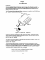
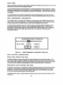
This manual describes the Gould Microprocessor Analysis Package (MAP). The MAP is a tool that
expands the test-debug capability of the Configurable Logic Analysis System 4000 (CLAS 4000). The
MAP disassembles captured information to convert executed object code into mnemonic code and
display the result on the video screen.
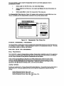
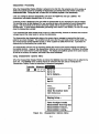
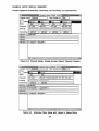
The MAP contains interface hardware and software components to be installed on the CLAS 4000 by the
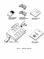
user. Typical MAP hardware is shown in Figure 1-1.
Figure 1·1. Typical MAP Components
Included in this manual is a microprocessor-to-logic analyzer pinout diagram, microprocessor-to-logic
analyzer connection data, screen displays of preprogrammed menus, and screen displays of captured
data presented in various disassembled formats.
HOW TO USE THIS MANUAL
The content in this manual is organized to present Standard MAP Features in Chapters 1 through 3 and
Unique MAP Features in Chapters 4 through 6.
Standard MAP Features
The Standard MAP Features (Chapters 1 through 3) describe common characteristics of the MAP
package which are the same for all microprocessor types. The information presented in these chapters is
intended to guide the user through the standard operating capabilities of the MAP. If specific information
is needed for a particular microprocessor type, refer to information contained in Chapters 4 through 6.
The Standard Features include the following types of information:
- Overview of MAP Hardware and Software Components (Chapter 1)
- Loading and Invoking the Disassembler (Chapter 2)
1-1
- Analyzer Setup (Chapter 2)
- Disassembler Operation (Chapter 3)
- Selecting Format Options (Chapter 3)
- Realignment of Data Screen (Chapter 3)
- Configuration Options (Chapter 3)
- Unloading the Disassembler (Chapter 3)
Unique MAP Features
The Unique MAP Features (Chapters 4 through 6) describe microprocessor dependent characteristics of
the MAP Package which are different for each microprocessor type. Refer to these chapters for detailed
information about connections for MAP components , microprocessor pin assignments, and unique
disassembler operations for the microprocessor type.
The Unique Features include the following types of information:
- MAP Components (Chapter 4)
- MAP Specification (Chapter 4)
- Target System Connections (Chapter 5)
- CLAS 4000 Equipment Connections (Chapter 5)
- Variations in Disassembler Operation (Chapter 6)
MAP HARDWARE COMPONENTS
Hardware Interface Requirements
The MAP hardware components consist of the Microprocessor Probe Adapter (which is used to interface
target system pins) and MAP Scrambler Box with attached cables (which is used to interface CLAS 4000
probe connections to the microprocessor probe adapter). These components are used to connect pins
on the target system microprocessor to assigned analyzer channel inputs on the CLAS 4000. The MAP
hardware interface allows the CLAS 4000 to capture data related to bus activity directly from the target
microprocessor pin location.
SCSI Pon Expansion and MAP Power Module
The MAP Scrambler Box may require input power supplied from the CLAS 4000 chassis. This power
interface is provided by the SCSI Port Expansion and MAP Power Module (Product No. A70042).
The SCSI module contains four conditioned +/- 5Volts power output connectors for interfacing the MAP
hardware and other accessories. The module also allows multiple SCSI devices to be connected in a
daisy-chain network to the CLAS 4000 chassis. The SCSI module is optional equipment and is not
included as a component in the MAP package. Contact your local Gould Sales office for additional
information on this component. When required for MAP operation, this equipment is described in the
Installation Connections section of Chapter 5.
1-2
MAP DISASSEMBLER SOFTWARE
The MAP software is a Disasserrt>ler Utility supplied on a single, 3.5-inch diskette which contains seven
types of files as follows:
- Disassembler Executable File
- Disassembler Setup File
- CLAS 4000 Resource File
- Sal'J1)1e Data File
- Sample Timing File
- Sample Symbol File
- Sample Label File
(filename ends in .BIN)
(filename ends in Setup)
(filename ends in Disassembler)
(filename ends in Sample Data)
(filename ends in Sample Timing)
(filename ends in Sample Symbols)
(filename ends in Sample Labels)
Disassembler Executable Fiie
The Disassembler Executable File contains the compiled and linked software for disassembly of a specific
microprocessor type on the CLAS 4000. The file format is structured so that it can be downloaded to, and
executed on the CLAS 4000. This file must reside in the Disassemblers folder which is contained
within the CLAS4000Foider folder.
Disassembler Setup Fiie
The Disassembler Setup File contains information that is unique to each Disassembler. The setup
information identifies the base format and clocking setup conditions for the Disassembler. The format can
be modified by the user without affecting disassembly processing, but any deletion from the base setup
parameters will render the disassembler unusable.
CLAS 4000 Resource Fiie
The Resource File contains all of the Disassembler Specific Macintosh code and resources to initialize the
Disassembler Parameters, an About Box, and an optional Disassembler Parameter Box.
Sample Flies
The Sample Files contain examples of recordings that are unique to each Disassembler. These files are
provided to demonstrate the capabilities and operating features of the Disassembler.
-The Sample Data File contains a recording of state data. The associated setup parameters are
included to allow the user to manipulate the recorded information.
-The Sample Timing File contains ALL of the available channels from the probe with pin numbers
and timing labels (e.g. "A7 DACK") in place of "Status 7". This is an asynchronous recording
intended for timing evaluation only and is not used for disassembly.
-The Sample Label File presents a table which contains at least four labels (e.g. Reset, Begin,
lnit, and Idle) for the code address group.
- The Sample Symbol File provides status information decoded for microprocessor cycle periods
which can be used for pattem definition.
Using the Dlsassembler
The disassembler evaluates object code recorded from the target system and displays this information in a
pseudo-assembly language form. The displayed information conforms to the chip manufacturer's
mnemonic code for the microprocessor instruction set.
The displayed information indicates the captured state of external bus activity that occurred at the
microprocessor pins. The user can manipulate the disassembled information to accomplish selective
review for the various disassembly modes.
1-3
The Disassembler evaluates recorded data to identify the processor cycles. It then attempts to identify the
program flow to decode the instructions. The Disassembler assumes the first recorded instruction to be
valid and all other instructions to be recorded continuously.
If the first recorded information is not the start of an instruction, or if all available information is not recorded
due to selective Trace Control, the disassembly may not be entirely acrurate. In this case, it is necessary
to re-synchronize the Disassembler to obtain the proper display. The procedure for realignment of the
display is described in Chapter 3.
Certain microprocessor types contain internal cache and program memory. These features must be
disabled to obtain a meaningful display of external microprocessor activity at the assigned pin/channel
location. Other types of microprocessors use the external cache which eliminates the need for user
intervention to enable and disable these circuit features. When applicable for MAP operation, this
information is provided in Chapter 6.
BASIC MAP OPERATING FEATURES
All MAP packages provide the following basic operating capabilities:
- Capture of Address, Data, and Control signals associated with microprocessor program
execution, and display cycle-by-cycle or summary by instruction sequences.
- Trigger on combinations of Bus Cycle Types; Input, Output, Memory Read/Write, Instruction
Fetch, and Interrupts.
- Display captured information in various listings using manufacturer's software architecture (e.g.
generate a listing with non-executed instructions deleted, or generate a listing with read/write
status deleted, etc.).
1-4
Chapter 2
LOADING AND INVOKING THE DISASSEMBLER
COPYING FILES TO HARD DISK
General
The CLAS 4000 application is driven by software contained in the folder named CLAS4000Folder.
This folder is installed on the Macintosh hard disk to implement CLAS 4000 operations.
The utility diskette supplied with the MAP components contains the CLAS4000Folder with the
Executable File, Setup File, Resource File and Sample Files described in Chapter 1. These files are used
to control disassembly processing for the CLAS 4000. These files must be copied to the hard disk as
described in the Installation procedure which follows.
The contents of the diskette must be placed in the correct directories on the Macintosh before the user
can boot the application.
Installation
If this is the first CLAS 4000 utility to be installed (i.e., there is no CLAS4000Folder on the hard disk),
copy the entire folder to the root directory of the hard disk. The main CLAS 4000 Application should
already be present in this directory.
If the CLAS4000Folder already exists, the Resource, Setup, and Sample files must be placed in the
CLAS4000Folder directory.
The Executable file must be placed into the subdirectory of the CLAS4000Folder titled
Disassemblers. This is necessary because the Disassembler interlace routines require a hard coded
directory structure. The CLAS4000Folder must be in the root directory to work properly.
If you are a first time user of the CLAS 4000 interfaced to the Macintosh computer, refer to the Macintosh
User's manual. This manual describes procedures for copying files to the hard disk and using folders to
organize stored information.
LOADING THE DISASSEMBLER
There are several ways to load the Disassembler utility. The first method is to double click the mouse on
the Setup Fiie in the CLAS4000Folder while in the Macintosh Desktop Window. This action loads the
CLAS 4000 Disassembler Setup parameters.
The second method is to Load the Disassembler with a setup from the CLAS 4000Flle Menu. This
should be used if the current setup is not appropriate for the disassembler. (The channel setup for
Address, Data, and Status fields, must be defined in the setup file in the same manner that was shipped
with the disassembler; otherwise, the data display information will be garbled.) To accomplish this, simply
load the next setup along with that of the disassembler. Running the Analyzer will then produce data in
the appropriate format for display.
The third method for loading the Disassembler is used when the setup is already compatible with the
Disassembler. The loading occurs by selecting the Load Utlllty menu item under the CLAS4000 empty
utility menu icon (see Figure 2-1). This action downloads the executable code and inserts the
disassembler in the setup.
-)
File
~ ~
<..,
Edit
Control
t
TrBnsfer
riii01
l!!!!J
Windows
--------------------------c.] c-·1 C]
Lo8d Utility •••
Figure 2-1.
Load Utlllty Menu Icon
2-1
The fourth method is used to load the Disassembler from the CLAS 4000 Application which is
accomplished as follows:
1.
Select Load from the Fiie menu, then select Next Setup.
2.
Select Load from the Fiie menu, then select Last Setup with Data (timing labels and
transfer).
3.
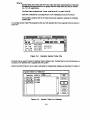
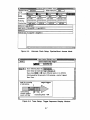
Select Load Utlllty to obtain the Disassembler Files dialog box.
The Disassembler Flies dialog box (Figure 2-2) appears after selecting the Load Utlllty menu item.
This box identifies all of the disassemblers contained in the currently selected folder.
e::::> Jim's herd •••
[) yyyyy Disassembler
a zzzzz Disassembler
Figure 2·2.
(
Ej<~<t
)
(
D1i1•<~
)
Disassembler Flies Dlalog Box
INVOKING DISASSEMBLY PROCESSING
The Disassembler is loaded and invoked by selecting the Disassembler filename from the Files dialog box
and clicking the mouse on Open, or double clicking the mouse on the Disassembler filename. The utility
is automatically loaded into memory and initialized.
ANALYZER SETUP FOR DISASSEMBLY
Setup
Requirements
The CLAS 4000 is setup for disassembly by loading a Disassembler compatible setup into the application.
The screens for Channel setup, along with the screens for Clock setup and Trace Control, are initialized
with the unique information for the particular Disassembler that was loaded.
These screens can be altered by using the CLAS 4000 standard setup method for each screen.
However, accurate disassembly can be assured only when the above screens contain the setup
information that was downloaded by the Disassembler. Additional columns of information can be
appended to the right side of the Setup screen , but none can be deleted.
Loading Symbols
Symbols are loaded into the Channel Setup Edit Symbol dialog box. The symbols may be either typed or
loaded from a file. If they are loaded from a file, the file must be of standard text using the following
formats:
Symbol String<tab OX>Hex Value <CR>
Symbol String<tab OX>Hex Value<tab> <CR>
Symbol String<tab OX>Hex Value <tab> Care Value <CR>
2-2
Where:
Symbol String, Hex Value, and Doni Care Value are ASCII representations of standard
Hexadecimal numbers which are no greater than the fields where they will be inserted
(i.e., 10, 8, 8 respectively).
The Care Value is optional and if used, rrust be set to 1 for each 'Care' Bit .
Each line is followed by a Carriage Return <CR> indicating the end of the record.
One symbol is used per line for as many lines as are required to express the complete
symbol table.
An example Symbol Table File prepared by the user with standard text in the required format is shown in
Figure 2-3.
;o
E!1I
IRddress Symbols
-~~-L~~;~:!;h~z~~~Llt~;
Test Bit
Oxffcla312
Ill
Set Flag
OxFFC1A336 OxFFFFFFFF
~
Clear Reg
Get Para•
Oxffc 19b50
OxFFC19E10
Figure 2·3.
Ox ff ff ff ff
&
~
Example Symbol Table Fiie
Symbols may be used for either the Address Field or Status Field. Sample files for each symbol type are
included on the diskette that is supplied with the system.
Address Symbols (Figure 2-4) are used to add labels to Disassembler displays as described in Chapter 3.
Symbol Table for "IRddress"
Symbols
ualue in:
T•st Bit
S•t Fl~
Clear R9Q
Get Pcrc::n
FFC1A324
FFC1A338
FFC19BS8
FFC19E48
I
(
HeH
~
Add
Dt~h~h~
I
OK
))
( Cancel )
Load
to
Figure 2·4.
Symbol Table for Address
2-3
saue
Status Symbols may be used to define Trace Control Patterns relative to microprocessor bus cycle types.
To use this feature, the Symbol Table is either entered or loaded in the Channel Setup Symbol Edit Mode
for the desired recording (i.e., Next, Last, or Reference). The selection of Next is normally used.
The desired symbol can then be selected in the Trace Control Pattern Definition window by double
clicking the mouse on the Status Pattern or using the Edit button to obtain the Symbol Selection Table
shown in Figure 2-5.
Symbol Selection Table
-------
Test Bit
Clear Reg
Get Param
Transition•
HHHHHHHHH
Test Bit
Pattern 2
Pattern 3
Pattern 4
Figure 2·5.
XXXXXXXX
XXXXXXXX
XXXXXXX>C
X
xxxxxxxx
)()()()()()()()(
)()()()()()()()(
)(
Symbol Selection Table
2-4
Chapter 3
DISASSEMBLER OPERATION
DISASSEMBLING THE DATA
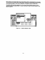
After loading is completed, the empty utility icon is replaced with the Disassembler menu icon (Figure 3-1 )
and its associated menu selections.
Control
~
t
Transfer Windows
Options
riii01
~l!.!.!!J
·-------------------·--Unload Utility •.•
Figure 3-1.
Disassembler Menu Icon for Last Data Recorded
The Disassembler Display Window (Figure 3-2) presents typical disassembled information. The display
window is entered by selecting either the LAST or the REFERENCE item from the Disassembler menu.
This selection determines what data is to be disassembled. Selecting the Title Choice from the
Disassembler Menu displays the revision level of the Disassembler software.
".. •)
File
Edit
Control
Transfer
Windows
Options
t
---=------- --
~-
~-
- - - - --
Disassembler [LR 1-Lest)
~
l@c2-c 1-I
C Sam I•
::
99835
00036
Address
Ob"ect
--
- -
oooosl samples
Status
eeee2F42 8998
9ee030F4 28168£16
FETCH
FETCH
=~~= ~=:~~::
~5
0e003DFF 87
eeea73A4 E8
0e082F36 8E
MRD
M~R
MUR
-~-
--~-
-
-
-----
Preuious
Mnemonic
AOC
CBX+SI J,AL
C160EJ.DL
= ~~!1,FUi
AttO
li!ill
c.1.. ~"~~~ .... ~~,,~~~- -'~~i:;~~~~ ............. F.;rcH ............. MQ~ ...... i~~~~.1.• ~1:1................ mm
99949
eeee73A2 8EDA
FETCH
MOV
OS • DX
Hili:
00041
99842
00843
::::~ =~~~~ :~
99945
99945
09945
90046
00846
C2 00047
8e048
80849
99050
08803SFD
ee0035FE
eee035FF
eee874E8
8ee074EB
eee074EE
eeea74F 1
8eee74F4
eee974F8
FETCH
FETCH
FETCH
FETCH
FETCH
FETCH
FETCH
FETCH
FETCH
E148
2A58C3
C3
B89280CO
FETCH
FETCH
FETCH
FETCH
FETCH
:::~~ eeee35FC
::~g~~ E~~==
148
eee53
00053
00054
00054
99955
8ee035FE
00004914
00004917
00004918
~CH
47
97
47
C0CBC3
CS7487
E82604
884406
36A32003
368C 1E22
Figure 3·2.
~=g.
1m1:
ai..
~
XCHG
I HC
XCHG
I HC
ROA
LOS
?CALL
AX, 0 I
0I
AX I 0 I
0I
BL. C3
SI, CSl+07J
S-2907 <00004917>
ililll
!H!H
mi~
mm
mm
!HW
mm
in!!:
mm
i:Hi~
11!1!1
LOOPZ
LOOPZ
SUB
RET
$+4A <00003646>
$+4A <00003648>
BL. CBX+S I +C3 J
Typical Disassembler Display Window
3-1
mW
mrn
i:!m
mm
mi!!
1HiH
Disassembly Processing
When the Disassembler Display Window is entered for the first time, the contents area of the window is
empty and a pause ocaJrs for completion of disassembly processing before the window is filled with
disassembled data. During this time, a Status Box will indicate progress of the disassembly.
If the user wishes to abort the disassembly, hold down the Apple key and type a period. The
disassembler will present disrupted data on the screen.
A spinning cursor is displayed to the user while the disassembler is busy decoding the data for display.
The spinning aJrsor is also displayed if a new recording is taken while viewing the current disassembly
display. The old contents of the screen will remain visible until the screen is updated with the new
decoded data. To avoid having disassembly processing occur when it is not needed, the user can simply
close the disassembler window.
If it is suspected that noise causes errors to occur in a data recording, increase or decrease the threshold
voltages beyond the noise levels to remove the disturbance.
The disassembler also disassembles data on the screen when a message is received that the format
patterns have been changed. This condition would OCaJr after the user loads another symbol table into
the Channel Setup Symbol definition screen, or when a pattern is edited from the list. It precedes the
disassembly by downloading the symbol table.
The disassembler columns may be moved by clicking the mouse on the column heading and shifting in
the desired direction. However, the disassembler columns can not be reordered; otherwise, this window
operates in the same manner as the state display. The display pane splitters operate in the same manner,
as well as the cursors, the markers, and most of the meru commands.
Using Disassembler Options Menu
When the Disassembler Display Window is entered, the Options menu item (Figure 3-3) is added to the
menu bar. The Options menu contains choices for selections that are used to manipulate the
Disassembler Display Window as described in subsequent paragraphs.
Transfer Windows
'='*
r- r-- r
[;J
..
~I 11 I
'-"·-
...._..
Go to Sample •••
------------------·--·-·-Get Cl
Get C2
..-..---------------------..
[ ompore
Clear the marker data
____
~(<=
EdU Refereru e
..__
................................ .................
-
___________________
_
.._._Display Setup ...
,
Force to object mode
Disassemble from top line
Disassembler format •••
Disassembler Conflg •••
Figure 3-3.
Disassembler Options Menu
3-2
Some of the Options Menu commands that are available in the State Window display are not available in
the Disassembler Window display and vice-versa as described below.
The following commands are available in the Disassembler Window but not in the State Window:
Force to Object Mode
Disassemble from Top Line
Disassembler Fonnat
Disassembler Configuration (when required by the specific disassembler)
The following commands are available in the State Window but not in the Disassembler Window:
Find*
Compare*
Edit Reference
*NOTE:
Despite the fact that Find and Compare commands are not available in the Disassembler
Window, the results are displayed in the Disassembler Window whenever they are used in
the State Window.
The user can change the displayed area of the Disassembler Window by using the Go to ••• cursor menu
items. The display window can also be manipulated either by using the scroll bars or by dragging the
cursor. If the display window has been manipulated by the scroll bar, and the user wishes to return to the
area in the recording where either cursor is located, choose the Go to C1 or Go to C2 menu item to
accomplish this action.
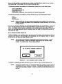
Go to Sample Number Dialog Box
The Go to Sample••• menu selection allows the user to view the display contents beginning with the
sample number selected. After selecting the Go to Sample ••• item, a dialog box (Figure 3-4) appears
so that the user may select the specific sample number.
NOTE:
The function for this selection is independent from the cursor movement. It merely
changes the display to show the information beginning from the selected sample
number. The cursors remain in their original positions.
Go to which sample number?
( Cancel )
OK
Figure 3·4.
Go to Sample Number Dialog Box
The Get C1 or Get C2 menu items position the cursor to the top of the currently displayed area.
NOTE:
Entering the sample number for the squares labeled C1 =or C2= is another method for
repositioning the cursor locations in memory. The Clear the marker data command
simply clears any search, compare, or marker information that was previously defined by
the user.
3-3
The Disassembier Fonnat••• command allows the user to define his preferences on such things as
font size, the choice to display step (level) data, and time stamp information. This command works exactly
the same for both the State and Disassermter Windows.
The Force to object mode command re-displays the current data in object format, with the smallest
instruction per line. This is useful when the data has a break in sequence, or when the recording did not
start on an instruction boundary.
The Disassemble from top llne command re-disassembles data from the top display line. This is used
in conjunction with the Force to object mode command to re-synchronize the Disassembler's internal
instruction counter with the data flow.
The last two commands are designed to be used together. When synchronization is lost, the user should
Force data to object mode, move down to a probable opcode location, and then return to normal
disassembly mode using the Disassemble from top llne command. The Disassembler is setup to
allow the user to do this as many times as needed.
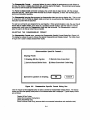
SELECTING THE DISASSEMBLER FORMAT
The Disassembler Format menu presents the Disassembler Specific Format Dialog Box (Figure 3-5).
This dialog box allows the user to choose the desired Disassembly and Display modes. The mode shown
in Figure 3-5 is used to display disassembly results.
Disassembler Specific Format •••
Display Mode:
O Display
O Delete
All Bus Cycles
O Delete Read/Write
Data
Non-Ewecuted
®Show EHecuted Code Only
l8J Enable symbols in display. l~[i i i i i i i i ioi i i iKi i i i i " ]
Figure 3·5.
( Cancel )
Disassembler Specific Format Dlalog Box
Click the mouse on the assigned button to select a choice for Disassembler Display Mode. The display
modes are filters that specify what portion of the disassembled data is displayed. Typical display modes
are as follows:
Display All Bus Cycles
Delete Non-Executed Instructions
Delete Read/Write Data
Show Executed Code Only (removes both non-executed instructions and read/write data)
3-4
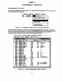
ENABLE SYMBOLS
Upon selecting the option for Enable symbols In display, a column is inserted in the disassembler
Display Window between the Status and Mnemonic column that is titled Labels.
The first column (Address) must be in Symbol Display Mode and a Symbol Table must be loaded.
The symbol is inserted at locations where an address matches a symbol from the Symbol Table or when a
decoded instruction references a specific Address (see Figure 3-6).
NOTE:
A Sample Address Symbol Table is included on the diskette supplied with the system.
§0
c1 =lo
Dis8ssembler (LR 1-L8st)
l@c2=l2s
l@c2-c1 =I
----
0002sl sBmples Pn~ucous
~
NeHt
C Sam le !Address DAddress Code
Data DRx CRx
Label
Mnemonic
C1 00000
FFC0978C
14420000
Idle Scode
Id
r2 r2 $0000
00001
FFC09790
F400C001
I.la i t Scode
j mp
r1
00003
FFC09794
24620000
Idle Scode
st
r3,r2,$0000
00004
FFC1A324
492200FF
Idle Scode Test Bit •ask
r9,r2,$00FF
00005
FFC1A328
704900DC
Idle Scode
cmp
r18,r9,$00DC
00006
FFC 1A32C
086A0003
Id I• Scod•
bb 1
<3>,r18, Set FI ag
00008
FFC1A338
58400000
Idle Scode Set Flag or
r2,re,seeee
00009
FFC 1A33C
143F0024
Id I• Scode
Id
r 1, r31, $0024
00010
FFC1A340
63FF0028
a.Jail Scode
addu
r31,r31,$0028
00012
FFC 1A344
F400C0e 1
Id Ie Scode
j 111p
r1
FFC 19850
086A0003
Idle Scode Cl ear Re bb1
<3 ),r10, $FFC19B5C
00015
00016
FFC19BS4
58400000
Idle Scode
or
r2,r0,$0800
00017
FFC19B58
C000008A
Idle Scode
bf"'
Get Para
00019
FFC 19E40
143F002C
Id 1e Scode Get Para Id
r 1, r31, S082C
00020
FFC19E44
171F0020
Uait Scode
Id
r24,r31,$0020
00022
FFC19E48
173F0024
Uait Scode
Id
r25,r31,$9024
~? .. ~~~~~.... fF.t;.t.~~~~ .............. -~~F:F.~~~~ .......... !~I~. ~c;:~<;t~ ••..•••.••••.•..• ~c;t~•••••• r:-~ L.r:-~ L.$~~~~- ..... .
00027
FFC 19E50
F400C001
Id 1e Scod•
j 111p
r1
00029
FFC0403C
5C40FFF8
Idle Scode
or.u
r2,r0,$FFF8
00030
FFC04040
58422000
Idle Scode
or
r2,r2,$2000
00031
FFC04044
CBFFFF78
Id Ie Scode
bsr
$FFC03E24
00033
FFC03E24
14420904
Idle Scod•
Id
r2,r2,$0004
00034
FFC03E28
F400C001
I.la i t Scode
j mp
r1
00036
FFC03E2C
F4E0600 1
Id I• Scode
addu
r 7, re, r 1
00037
FFC04048
0002FFE8
Idle Scode
bb0
<0>,r2,$FFC03FE8
00039
FFC03FE8
SC40FFF8
Idle Scod•
or.u
r2,r8,$FFF8
00040
FFC03FEC
58422020
ldl• Scode
or
r2,r2,$2020
00041
FFC03FF0
CBFFFF80
Id 1e Scode
bsr
$FFC03E24
Figure 3·6. Symbol Column lnsenlon In Data Dlsplay Window
SELECTING
DISASSEMBLER CONFIGURATION
The Disassembler Conflg ••• menu selection is available when the current disassembler has
parameters that will not fit into the choices available above. These conditions are defined inside the
disassembler resource file, and will vary from one disassembler to another.
Typically, this menu is used to specify operating modes of the target microprocessor or to provide the
value of internal registers which cannot be determined from recorded data. This information is described
in Chapter 6 when required for a specific Disassembler.
UNLOADING THE DISASSEMBLER
The Disassembler is unloaded by clicking the mouse on the Unload UtllHy menu item on the icon
menu bar (See Figure 3-1 ). This action will cause the Disassembler to unload. The Setup information is
purged from the CLAS 4000 and the Utility icon becomes grayed to indicate the utility is inactive. If a
setup containing a disassembler is loaded on top of another disassembler, the old one is automatically
unloaded.
3-5
Chapter 4
29000 MAP SPECIFICATIONS
PHYSICAL DIMENSIONS AND WEIGHT
Height:
2.5 inches (6.4 cm)
Width:
8.5 inches (21.6 cm)
Depth:
9.25 inches (23.5 cm)
Cables:
13.5 inches (34 cm) long
Weight:
3.4 lbs., (1.5 kg) with Probe Adapter and attached cables
ELECTRICAL
CHARACTERISTICS
Loading (Signal Inputs)
Input Impedance:
Probe load for all signals except DREQN and IREQN is 1
megohm shunted by 8pf. Maximum current for signals is +/- 5uA
Probe load for DREQN and IREQN is one TTL for each signal
Loading (Ground/Reference Input)
Input Resistance:
Less than 1 ohm referenced to target system ground and
approximately 18K ohms referenced to logic analyzer ground
Ground Difference
Immunity:
+/- 0.25 Volt maximum between logic analyzer ground
and target system ground
POWER
Supplied from CLAS 4000:
May require SCSI Port Expansion and MAP Power Option
to provide 5 Volts DC
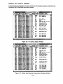
MAP COMPONENTS
The 29000 Microprocessor Analysis Package (Product No. A70043) consists of the following
components which are shown in Figure 4-1 :
- 29000 Scrambler Box (with attached signal cables and power cord)
- Probe Adapter Assembly
-Two Clock Probe Interface Adapters
- One 29000 Disassembler Diskette
- Users Manual
4-1
OCESSOR
MICROP~DAPTER
0
CLOCK ~'::O~~APTER
INTEOR19F:1055-10
.
P/N
·
~~ 0~~2-0380-10
SCRAMBLER
~/~E~1 :2 _0286-10
ASSEMBLY
Figure 4·1.
SOFTW ARE DISKETTE
O
PIN 0192-0480-1
'
29000 MAP Components
4-2
MANUAL
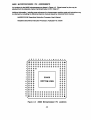
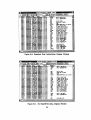
29000 MICROPROCESSOR PIN ASSIGNMENTS
Pin locations for the 29000 microprocessor are shown in Figure 4-2. Signal names for pins may be
obtained from the reference manual mentioned below or from Table 5-1.
Additional information, including cross references for microprocessor machine code and instructions may
be obtained by consulting the following reference manuals issued by Advanced Micro Devices:
AM29000 32-Bit Streamlined Instruction Processor User's Manual
AM29000 Streamlined Instruction Processor, Publication No. 09075
A 9
C
D
E
F G
H J
K L
M N P
R
T
U
•@@®®®@®®®@®®®@®•
2
®®®®®®®®®®@®@@®@®
3 ®®®®@®®®®®®®®®®®®
• ®®®®
®@@
5 ®®@
@®®
• ®®®
@®®
7
® ® @·
® ® ®
29000
@ @@
• ® ® ®
@®®
• ®®®
10 ® ® ®
BOTTOM VIEW
® ® ®
1t
®®®
@@®
12
®®@
@®@
11
®®®
@®®
1,
®®®
®@®
~ ®®®®@®®@®®®®®®®@@
11
@®@®@®®®®®®®®®®®®
17
•@@®®®®®®®®®®®@@•
1
Figure 4·2
29000 Microprocessor Pin Locations
4-3
Chapter 5
INSTALLATION
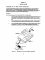
SCRAMBLER BOX TO TARGET SYSTEM CONNECTIONS
The 29000 microprocessor chip l'TlJSt be removed from the target system and the Probe Adapter is
installed in its place. The microprocessor chip is then inserted into the probe adapter via the Zero
Insertion Force (ZIF) socket. The Probe Adapter is connected to the Scrambler Box with three attached
cables as shown in Figure 5-1. The Probe Adapter contains one jumper connection (W.1) which is
described in Chapter 6 (see description of INCLK Signal Loading).
Procedure
Use the following procedure to connect Scrambler Box to the target system:
1.
Remove the 29000 microprocessor chip from target system socket and install the base of
probe adapter into the target system socket. Observe the location of pin A1 on probe
adapter which must mate with pin A1 on the target system socket for correct alignment of
pins.
2.
Install the microprocessor chip on probe adapter via the ZIF socket. Ensure pin locations
on the microprocessor chip are aligned with corresponding pins on the probe adapter .
3.
Verify the three ribbon cables from scrambler box are securely fastened to probe adapter
at connectors T1, T2, and T3. (The MAP package is shipped with these cables
connected to the probe adapter; however, they could become loose during transit.)
Figure 5-1.
Scrambler Box to Probe Adapter Connections
5-1
SCRAMBLER BOX TO CLAS 4000 CONNECTIONS
The clock interface cables attached to the Scrambler Box must be connected to the CLAS 4000 and input
probes for the CLAS 4000 are connected to the Scrambler Box as shown in Figure 5-2. Probe
connectors on top of the Scrambler Box are labeled W, X, Y, and Z to identify the location for a
corresponding analyzer probe.
The two Clock Probe Interface Adapters supplied with the MAP package must be installed on the Z
Channel connector at Data Boards A and B. These adapters are used to connect both the analyzer probe
cable and Scrambler Box clock interface cable to the Z connector.
The two Scrambler Box Clock Interface cables contain16-pin connectors which plug into mating
connectors on the Clock Probe Adapters. The 100 MHz coaxial cable on the Scrambler Box attaches to a
jack on the CLAS 4000 Control Board Panel.
The 29000 MAP Scrambler Box receives +5 Volts power input from the CLAS 4000. The power is
supplied from the SCSI Port Expansion and MAP Power Module (Product No. A70042). This option must
be installed on the CLAS 4000 chassis to power the MAP Scrambler Box for Pipeline/Burst Access mode.
(This option is not required for Simple Access mode.)
Procedure
Use the following procedure to connect the the Scrambler Box to the CLAS 4000:
1.
Ensure AC power is off at CLAS 4000 prior to connecting the Scrambler Box.
2.
Remove analyzer probe cables from Z Channel location on Data Boards A and B. Install a
clock probe adapter at each of the Z Channel connectors. Connect analyzer probe
cables to the adapter.
3.
Connect two clock input signal cables and coaxial cable from Scrambler Box to CLAS
4000 as follows:
a)
NOTE:
NOTE:
Locate the clock interface cable which is labeled POWER/GROUND
THRESHOLD. Connect this cable to the mating connector on Clock Probe
Adapter at Data Board A.
This cable supplies signals that control the synchronization of clocks and must be
connected to the adapter at Data Board A.
b)
Connect the other clock input cable to Clock Probe Adapter at Data Board B.
c)
Connect the 100 MHz coaxial cable to one of the CLK OUT jacks on CLAS 4000
Control Panel.
The 5-Volt power requirement for scrambler box is determined by the clocking scheme
setup. Refer to description of 29000 Clocking Considerations in Chapter 6. If power
is not required for the user's setup, omit Step 4. If power is required, perform Step 4.
4.
Connect the Scrambler Box power cord to one of the 5-Volt SCSI connectors at lower
front panel of CLAS 4000 chassis.
5.
Remove flying leads and grabbers from analyzer probe connectors (if attached) and
connect seven probes, W, W, X , X, Y, Y, and Z into corresponding Scrambler Box
locations as follows:
a)
Connect W and X probes from Data Board A to corresponding W and X probe
locations on right side of Scrambler Box (see orientation in Figure 5-2).
b)
Connect W and X probes from Data Board B to corresponding W and X probe
locations on left side of Scrambler Box .
5-2
c)
Connect Y probe from Data Board A to Y probe location on right side of Scrambler
Box.
d)
Connect Z probe from clock probe adapter at Data Board A to Z probe location on
Scrambler Box .
e)
Connect Y probe at Data Board B to Y probe location on left side of Scrambler Box.
,----- ------......
CLAS 4000
FRONT PANEL
I
............ ......_,
I
--·----------....... .....
Ii
ii,: ( _/
DATA BOARD A
CLOCK PROBE
ADAPTER
111
I
I
11
I
I
I _L~RESHOLD~ABLE
, _
-
CABLE
SCRAMBLER BOX
PROBE CONNECTOR
(TYPICAL)
Figure 5·2.
Scrambler Box to CLAS 4000 Connections
5-3
J~
CLOCK POWER/GROLMD
~CLOCK SIGNAL
I
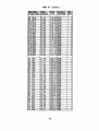
MICROPROCESSOR PINOUTS TO LOGIC ANALYZER
Signals for the following lines (143 total) are transferred from the 29000 microprocessor in the target
system under test to the Scrambler Box :
32 Data Lines
32 Address Lines
32 Instruction Lines
(DO- D31)
( AO-A31)
( 10 - 131 )
47 Status and Control Lines
These signals are also transferred from the Scrambler Box to the assigned Logic Analyzer channel in the
CLAS 4000.
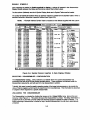
The list in Table 5-1 identifies the assigned Signal Name/Function for each 29000 pin, the Target Head
pin connections, MAP Scrambler Board pin connections, and the corresponding Logic Analyzer channel
connections. Schematic diagrams for circuit connections are provided in Chapter 6.
The following conventions are used in Table 5-1:
- The abbreviation GND indicates ground.
- The asterisk (*) character following the signal name indicates active-low logic level.
5-4
Table 5·1. 29000 MICROPROCESSOR-TO-LOGIC ANALYZER CONNECTIONS
CableFGA Stg_nal
Pin__f of 29000 Conductor
M16
M17
R15
T16
T17
P15
R16
R17
P16
P17
L16
L17
K16
K17
J17
J1S
J16
H17
H16
G17
G16
F17
G15
E17
F16
F15
017
E16
016
C17
817
015
AOO
A01
A02
A03
A04
AOS
A06
A07
A08
A09
A10
A11
A12
A13
A14
A15
A16
A17
A18
A19
A20
A21
A22
A23
A24
A2S
A26
A27
A28
A29
A30
A31
T3-20
T3-26
T2-11
T3-04
T3-10
T2-09
T3-08
T3-14
T3-12
T3-18
T2-20,
T2-26
T2-24
T2-01
T2-47
T1-02
T2-03
T2-43
T2-49
T2-30
T2-28
T3-28
T3-46
T3-32
T3-24
T2-45
T3-36
T3-30
T3-34
T3-40
T3-44
T2-41
84
BS
A4
000
001
002
003
004
005
006
007
008
009
010
011
T1-46
T1-45
T1-50
T1-43
T1 -39
T1-49
T1-47
T2-37
T1 ·31
T1 -27
T1-33
T1 -29
C6
AS
86
AS
C7
87
A7
88
AS
Probe
Pint
Channel I
CLAS 4000
Data
Bd.#
J01-03
JO 1-05
J01-07
J01-09
J01-11
J01-13
J01-15
J01-17
J01-19
J01-21
JO 1-23
J01-25
J02-03
J02-05
J02-07
J02-09
J02-11
J02-13
J02-15
J02-17
J02-19
. J02-21
J02-23
J02-25
J03-03
J03-05
J03-07
J03-09
J03-11
J03-13
J03-15
J03-17
CHOO
CH01
CH02
CH03
CH04
CHOS
CH06
CH07
CH08
CH09
CH10
CH11
CH12
CH13
CH14
CH15
CH16
CH17
CH18
CH19
CH20
CH21
CH22
CH23
CH24
CH25
CH26
CH27
CH28
CH29
CH30
CH31
1
1
1
1
1
1
1
1
1
1
1
1
1
1
1
1
1
1
1
1
1
1
1
1
1
1
1
1
1
1
1
1
J09-03
J09-0S
J09-07
J09-09
J09-11
J09-13
J09-15
J09·17
J09-19
J09·21
J09-23
J09·25
CHOO
CH01
CH02
CH03
CH04
CHOS
CH06
CH07
CH08
CH09
CH10
CH11
2
2
2
2
2
2
2
2
2
2
2
2
5-5
Table 5·1 ( Cont'd.)
CableFG\ S]ilnal
Pln_f of 29000 Conductor
Probe
Pini
Channel I
CLAS 4000
A9
89
A10
810
A11
811
A12
812
A13
A14
C12
813
914
A15
C13
A16
815
816
C15
C16
012
013
014
015
016
017
018
019
020
021
022
023
024
025
026
027
028
029
030
031
T1-37
T1-35
T2-50
T2-48
T2-46
T2-44
T2-40
T2-36
T2-42
T2-29
T2-32
T2-38
T2-33
T2-23
T2-34
T3-48
T2-27
T3-42
T2-31
T3-38
J 10-03
J 10-05
J 10-07
J10-09
J 1 0-11
J 10-13
J 10-15
J 10-1 7
J 10-1 9
J 10-21
J 10-23
J 10-25
J 11-03
J 11-05
J 11-07
J 11-09
J11-11
J11-13
J11-15
J11-17
CH12
CH13
CH14
CH15
CH16
CH17
CH18
CH19
CH20
CH21
CH22
CH23
CH24
CH25
CH26
CH27
CH28
CH29
CH30
CH31
A3
A2
100
101
102
103
104
105
106
107
108
109
110
111
112
113
14
15
16
17
18
19
20
21
22
23
24
25
26
T1 -48
T1 -42
T1 -41
T1 -44
T1-34
T1-38
T1 -36
T1 -32
T3-47
T3-49
T3-43
T3-45
T3-39
T3-41
T1 -30
T3-35
T3-37
T1-28
T3-31
T3-33
T3-29
T2-39
T3-27
T3-25
T3-23
T3-t9
T3-21
J03-19
J03-21
J03-23
J03-25
J04-03
J04-05
J04-07
J04-09
J04-11
J04-13
J04-15
J04-17
J 04-1 9
J04-21
J04-23
J04-25
J05-03
J05-05
J05-07
J05-09
J 05-11
J05-13
J 05-15
J 05-17
JOS-19
J05-21
JOS-23
CH32
CH33
CH34
CH35
CH36
CH37
CH38
CH39
CH40
CH41
CH42
CH43
CH44
CH45
CH46
CH47
CH48
CH49
CHSO
CH51
CH52
CH53
CH54
CH55
CH56
CH57
CH58
C4
83
C3
82
81
03
C2
C1
02
01
E2
E1
F3
F2
F1
m
G2
G1
H1
H3
H2
J1
J2
K2
K1
5-6
Data
Bd.t
2
2
2
2
2
2
2
2
2
2
2
2
2
2
2
2
2
2
2
2
1
1
1
1
1
1
1
1
1
1
1
1
1
1
1
1
1
1
1
1
1
1
1
1
1
1
1
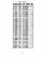
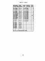
Table 5-1 ( Cont'd.)
S]inal
CaJllePlnJ of 29000 Conductor
~
Probe
Pin•
Channel•
CLAS 4000
Data
Bd.t
127
128
129
130
131
T3-17
T3-15
T3-13
T3-11
T3-09
J05-25
J06-03
J06-05
J06-07
J0&-0·9
CH59
CH60
CH61
CH62
CH63
1
1
1
1
1
BGRT•
BINV•
aRea·
coA·
coA·
CNTLO
CNTL1
T1 -15
T1-19
T1 -18
T1 -16
T1 -16
T3-03
T3-05
J 12-03
J06-11
J 12-05
J12-07
J12-07
J 12-09
J 1 2-11
CH36
CH64
CH37
CH94
CH38
CH39
CH40
2
1
2
1 &2
2
2
2
R9
T10
U13
U12
R4
T3
R3
R3
T7
U6
T6
DBREQ•
oRea·
OREQTO
DREOT1
DBACK•
DERR•
oRov·
DROY•
INTRNO
INTRN1
INTRN2
INTRN3
IBR ea·
U9 1Rea·
U15 IREQT
U4 IBACK•
U3 IERR•
T1
INCLK
T4
1Rov·
T4
IRDVT11 LOCK•
T2-13
T2-06
T2-14
T2-08
T 1-11
T1-10
T1 -22
T1 -22
T1 -21
T1 -05
T1 -03
T1-09
T1-23
T1 -17
T2-21
T1-04
T1-06
T1 -12
T1 -13
T1 -13
T2-10
J 1 2-13
J06-13
J06-15
J06-17
J 1 2-1 5
J 1 2-1 7
J 1 2-19
J 1 2-1 9
J11-19
J11-21
J11-23
J11-25
J06-19
J06-21
J12-21
J06-23
J12-23
J 12.;25
J06-25
J06-25
J07-03
CH41
CH65
CH66
CH67
CH42
CH43
CH44
CH90
CH32
CH33
CH34
CH35
CH68
CH69
CH45
CH70
CH46
CH47
CH71
CH91
CH72
2
1
1
1
2
2
2
1 &2
2
2
2
2
1
1
2
1
2
2
1
1 &2
1
N17 MPGMO
N16 MPGM1
T12 MSERR
T3-22
T3-18
T2-12
J07-05 CH73
J07-07 CH74
J 13-03 CH48
1
1
2
R14 OPTO
T15 OPT1
U16 OPT2
T2-15
T2-17
T3-02
J07-09 CH75
J07-11 CH76
J07-13 CH77
1
1
1
T1 -14
T1-20
T2-16
T2-02
J07-15
J13-05
J 13-07
J07-17
1
2
2
1
L1
L2
M1
M2
N1
T9
TS
T2
T2
R2
P2
. P1
us
us
U02
P03
R10
U10
PEN•
PWRCLK
PDA•
PtA•
5-7
CH78
CH49
CHSO
CH79
Table 5-1 ( Cont'd.)
Cable~ Sta_nal
PinJ of 29000 Conductor
Probe
Pint
U11 R/W•
R01 RESEr'
T2-04
T3·01
J 13-09 CH51
J 1 3-11 CH52
T2-18
T2-25
T2-22
T2-19
T1 -24
T1 -24
T3-07
T1 -25
T1 -01
T1-07
J 13-13
J 1 3-1 5
J 13-1 7
J07-19
J 1 3-1 9
J 13-19
J13-21
J 13-23
J 13-25
J 14-03
CH53
CH54
CH55
CH80
CH56
CH92
CH57
CH58
CH59
CH60
2
2
2
1
2
1& 2
C14 ~
T2-35
J 14-05 CH61
2
CN>
CN>
CN>
CN>
CN>
CN>
CN>
T2-05
T1 -40
T3-50
T2-07
T1-08
T1 -26
T3·06
T13
U14
R12
T14
N03
N03
N02
U07
R07
TOS
M14
A01
A17
N15
U01
M03
U17
STATO
STAT1
STAT2
SUP/US*
S1SClK
SVSClK
TEST*
TRAPO*
TRAP1•
WAR*
Channel I
CLAS 4000
J01 TO J14 ALL ODD PINS SHORT TO GND.
5-8
Data
Bd.t
2
2
2
2
2
2
Chapter 6
SPECIAL OPERATING FEATURES
GENERAL
This chapter describes special operating features for the 29000 MAP Disassembler as related to unique
characteristics of the AM29000 microprocessor. Example screens are provided for Setup Display
Windows and Data Display Windows.
Reference: AMD Am29000 32-Bit Streamlined Instruction Processor User's Manual
INSTRUCTION
PROCESSING
Branch Instructions
The Am29000 calculates branch addresses for direct branches (both CALL and JMPx) in one of two ways.
The first method sign-extends the concatenated values of the RC and RB instruction fields, shifts the
whole thing left two bits (32-bit word alignment), and adds the result to the current PC. The second
method zero-extends the concatenated values of the RC and RB instruction fields and shifts the whole
thing left two bits (32-bit word alignment) to produce an absolute address value.
The disassembler displays the calculated value instead of the actual displacement value contained in the
instruction.
Although the Am29000 allows placement of two consecutive branch instructions, the delayed branching
feature of the Am29000 may produce unexpected results unless the programmer specifically designed
the code to take advantage of this feature. See pages 7-24 and 7-25 of the Reference Am29000 Users
Manual for further information on this effect.
As an aid to programmers, the disassembler places an exclamation point(!) in front of any branch
instruction that immediately follows another branch instruction.
Trap Instructions
Trap instructions (EMULATE, ASxxx) contain an eight-bit vector number that is used to create a vector
address in one of two ways. If the Vector Fetch bit in the Configuration Register is set, the vector number
replaces bits 9 - 2 of the Vector Area Base register and the result is used to fetch the actual trap vector
from memory (indirect method). If the Vector Fetch bit is reset, the vector number replaces bits 15 - 8 of
the Vector Area Base register and the result is used to fetch the first trap instruction from memory (direct
method).
The disassembler can not determine the state of the Vector Fetch bit directly, so it assumes the bit is
cleared (Indirect Mode). The user may select Direct Mode by first selecting the 'Disassembler
Configuration' menu entry from the 'Options' menu, and then clicking the mouse on the selection button
next to the desired mode (see description of 29000 Disassembler Configuration).
The disassembler displays the calculated value (surrounded by angle brackets if indirect), followed by the
actual eight-bit vector number as a decimal number in parenthesis.
The Am29000 causes a Protection Violation trap to occur if the processor is in User mode and attempts to
execute a trap with a vector number of O - 63. The disassembler marks such trap instructions with an
exclamation point (!) prior to the mnemonic.
6-1
REGISTER
ASSIGNMENTS
Registers are identified by the designators IP, SP, GRxxx and LRxxx, corresponding to the 29000
absolute register numbers according to the following table:
ABSOLUTE#
0
1
2-63
64 - 127
128 - 255
IDENTIFIER
IP
SP
GRxxx
LRxxx
(Indirect Pointer)
(Stack Pointer)
Global Register 2 - 63 (Unimplemented)
Global Register 64 - 127
Local Register O - 127
ILLEGAL OPCODE
If the 29000 Disassembler encounters an illegal opcode, the message -ILLEGAL- is displayed in the
mnemonic field. If the opcode is legal, but one or more of the operands is illegal, the mnemonic will be
displayed, along with any operands that were legally decoded. If an illegal opcode is encountered, the
Comment column will contain the message '## Illegal Operand'.
Instructions that reference Global registers 2 - 63 (unimplemented), will correctly display the global register
in question, but will also be marked '! ! Illegal Operand'.
The instruction coding for 'ASEQ xx,GR1 ,GR1' is generally considered and used as a NOP (see
Reference Am29000 User's Manual, page 7-13), since it does not perform any action (GR1 will always be
equal to GR1 ).
The disassembler, therefore, will display the psuedo-mnemonic of 'NOP' whenever this instruction
encoding is found.
MESSAGES
Trap Messages
The messages presented below are displayed in the Comment column for lines that contain either trap
instructions, or the first instruction of a trap routine. The messages are derived from the trap vector list in
the Reference Am29000 User's Manual, pages 3-45 and 3-46.
Trap
O
1
2
3
4
5
6
7
8
9
1O
11
12
13
14
15
16
17
18
Message
@@ Illegal Opcode
@@ Unaligned Access
@@ Out of Range
@@ Coprocessor Not Present
@@ Coprocessor Exception
@@ Protection Violation
@@ Instr Access Exception
@@ Data Access Exception
@@User Instr TLB Miss
@@ User Data TLB Miss
@@ Super Instr TLB Miss
@@ Super Data TLB Miss
@@ Instr TLB Prot Violation
@@ Data TLB Prot Violation
@@Timer
@@Trace
@@*INTRO
@@*INTR1
@@*INTR2
6-2
Trap Messages (Cont.)
19
20
21
@@*INTR3
@@*TRAPO
@@*TRAP1
22-23
@@ Reserved Trap
24-31
@@ Reserved Emulation Trap
32
33
34
35
36
@@MULTIPLY
@@DIVIDE
@@MULTIPLU
@@DIVIDU
@@CONVER
37-41
@@ Reserved Emulation Trap
42
43
44
45
46
47
48
49
50
51
52
53
54
55
@@FEQ
@@DEQ
@@FGT
@@DGT
@@FGE
@@DGE
@@FADD
@@DADD
@@FSUB
@@DSUB
@@FMUL
@@DMUL
@@FDIV
@@DDI
56-63
@@ Reserved Emulation Trap
64-255
@@ Assert/EM ULATE Trap
Status Messages
The Status column messages are interpreted as follows:
Message
U Fetch
UData
Ul/O
UCP
UData
(User)
Wr
Wr
Wr
Rd
1/0
Rd
UCP
Rd
S Fetch (Supervisor)
SData Wr
Wr
Sl/O
SCP
Wr
SData Rd
u
s 110
SCP
Rd
Rd
SUP/US
*IRDY R/W
0
0
0
1
1
1
1
1
1
0
0
0
0
0
1
1
1
1
1
1
1
0
1
1
1
1
1
1
6-3
x
0
0
0
1
1
1
x
0
0
0
1
1
1
DREQT1
DREQTO
x
0
0
1
0
0
x
0
1
x
0
1
x
x
0
1
x
0
1
x
x
0
0
·1
0
0
1
1
BURST MODE
When the Am29000 is operating in 'Burst' Mode, it generates one address and then clocks in one or more
data/instruction words without changing the address.
If the disassembler detects Burst Mode operation, it artificially generates the missing addresses. Artificial
addresses are marked as such by an asterisk (*) in the most significant digit. The first address of a Burst is
not marked in this fashion (it is the actual address output by the processor), and can be used to obtain the
missing digit.
If a recording begins in the middle of a Burst Mode access, the disassembler can not know how many
accesses have occurred since the start of the burst; therefore, the generated address may be incorrect.
29000 DISASSEMBLER CONFIGURATION
The Am29000 Vector Area Base (VAB) Register is a 32-bit register in the Am29000 that contains the
upper 16 bits of all trap vector addresses. The 29000 Disassembler allows the user to specify the value
currently being used by the 29000 processor to allow accurate tagging of trap execution.
To change from the default trap vector of 0, click the mouse on the Disassembler Configuration menu
entry under the Options menu (Figure 6-1) when a disassembler window is active. Enter the most
significant 16 bits of the desired trap vector. Note that the lower 16 bits are always zero, as indicated by
the 4,0 digits to the right of the 6-digit numerical entry field. The trap vector value is entered in
Hexadecimal notation.
Rm29000 Disassembler Configuration
Uector Rrea Base:
Uector Fetch:
®Direct
n
Figure 6·1.
jlmnmloooo (HeHadecimal)
OK
1
0
Indirect
Cancel
29000 Disassembler Configuration Dialog Box
29000 CLOCKING CONSIDERATIONS
Simple Access (Default) Clock Setup
The 29000 operates in various modes which may require alteration of the clock setup condition. The
default setup condition supplied on diskette is intended for simple access for both instructions and data.
In this default mode, all Address, Data and Status is latched on the rising .edge of the target System Clock
(Channel 92) and is mastered by AN Ding signals for DADY (Channel 90) and IRDY (Channel 91 ).
Pipeline/Burst Access (Alternate) Clock Setup
For Pipeline or Burst access, it is necessary to latch the appropriate addresses during the proper IREQ or
DREQ cycle. These signals are ANDed on the scrambler board for this contingency, and the result is
available on Channel 93. By ORing this signal with the target system clock, the Address Latch signal
occurs only during the appropriate part of the address cycle.
The alternate Clock Setup to recognize Pipeline and Burst access for both Instruction and Data is shown
in Figure 6-4.
6-4
NOTE:
To use this signal in the clock setup, +5 Volts must be supplied to the scrambler
board via the attached power cord provided with the MAP Package. The +5 Volts can
be supplied by the user's power source or by the optional SCSI Port Expansion and
MAP Power Module on the CLAS 4000.
Additionally, the CDA signal is available on Channel 94 for clocking the write cycle to a coprocessor. This
signal may be either ANDed or ORed with the master clock depending upon how this signal is used in the
target system.
INCLK Signal Loading
Some target system configurations may experience input loading of the INCLK signal which is supplied to
Analyzer channel 47 of Data Board 2. A single-position jumper connection (W1) is located on the Probe
Adapter. Removing this jumper allows the user to disconnect the INCLK signal from the MAP.
6-5
EXAMPLE SETUP DISPLAY WINDOWS
Example displays for Channel Setup, Clock Setup, and Trace Setup are presented below.
1
~0
Somple clock:
M
L8 bet:
RadiH
I
Channel Setup (29000-NeHt)
Time Stamp at:
sons
llBICo•d•e---
St at us
I
EHternel
Address
I
_I_H_eH_ _ _ I
I
I
HeH
) ~63-A32
Channels
[A31-A00
Polarity
l++++++++++++I j++++++++++++I
Clocked by
I
LATCH O
II
LATCH O
!!Oa!!tl!!a!!!!!!!!!!!!!!!!!!!
I
HeH
] (631-600
I
HeH
I
---i
) (855-653 A70 )
j++++++++++++j j+++++++++++ I
II
LATCH O
II
LATCH O
LATCH 0 =( s sclk(92} )
LRTCH 1 =
LATCH 2 =
MASTER CUC =( ird
Figure 6·2. Channel Setup, Simple Access Default Clocklng Scheme
S8mple clock:
M
Channel Setup [29000-NeHt]
Time St8mp at:
EHternal
L 8 be I: Pl!!!!Da!!t!!!a!!!!!!!!!!!!!!!!!
RadiH
I
HeH
!!!!!!!!!!!!!!!!!!!!!!!!!!!!!!!!!!!!!!!!!!!!~
Channels
(631-600
Polarity
l++++++++++++I !+++++++++++
Clocked by
I
LATCH O
sons
!!!St!!a!!t!!ui!s
II
HeH
I
] (655-653 A70 642 A80 6H A71 651 A67-A66
I I!:::==============================::::
LRTCH O
LATCH 0 =( s sclk(92) )
add latch 1:( i*dreq(93) ) + ( s scllc(92) )
LATCH 2 •
Figure 6-3.
Alternate Clock Setup with Values In Status Block
6-6
§0
Ctlonnel Setup [29000-NeHt)
Time Stomp ot:
Polarity
!++++++~..+++++! j++++++++++++j
Clocked by
I
odd letch
II
sons
LATCH O
LATCH 0 =( s sclk(92) )
add latch =( i*dreq(93) ) + ( s sclk(92) )
LATCH 2 •
Figure 6·4.
Alternate Clock Setup, Plpellne/Burst Access Mode
iD
Trace Control (29000-NeHt)
Taslcs
ITnslcs: Simple Edge Trigger
llallBJ
lstep
#i
ILmls Fr"= 12 II
Store filtering input to •HHHHHHHHH
Until (felse to true) input is l=Pettern 1
I;
Then store 12048
I~ more filtered inputs (2 to 65535);
(2048 would be SO percent of 4K memory = center trigger)
Then Stop
Look for re-entry
of subroutine
Edge Trigger
ouerwriting
pushes trigger
point left (up)
I ncreuing Time --..
Figure 6·5. Trace Setup, Trigger Sequence Display Window
6-7
EXAMPLE DATA DISPLAY WINDOWS
Example displays are presented for All Cycles, Deletion of Non-Executed Instructions, Read/Write Only
Instructions, and No Read/Write Instructions Executed.
iD
Disassembler [29000-Last)
Preuious
00010
00011
00012
89913
00014
00015
00016
08817
00018
09919
00020
00021
00022
00023
00024
0ee2s
09926
00021
09928
00029
00030
00031
00032
08833
00034
00835
89836
00031
eeee9C64
0eee9C68
eeee9C6C
88999C78
88889C78
88889C7C
0000gc99
88989C84
00ee9C88
00989E1C
aaee9E28
80989E24
eeee9E28
881849Ae
09889E2C
s0eeeees
88889£38
ee889E34
seeeeeea
88889E38
88889E3C
901849A4
88999£48
e0eeeee8
0000ge:44
80089E48
00eege:4c
99eege:se
62798679
ACee7984
10499101
A8FE884F
15018118
15687588
c0eee080
5641817F
AeFFeeFS
15798A14
16887879
16887978
917779FF
91777gFF
1Eee&378
1E988378
15798A18
16987979
16887979
16887979
917879FF
917879FF
91797791
91797781
61797980
AC887914
91797788
63797988
eeet3FFF s F•tch
eeeeeeFF s F•tch
eeee3FFF s F•tch
eee83FFF s F•tch
eee824FF S Fetch
800eFFFF s F•tch
eee03FFF s Fetch
eeeeFFFF s Fetch
0ee03FFF s Fetch
99983FFF S Fetch
0eeeFFFF s F•tch
eeeeFFFF s Fetch
eeeaFFFF s Fetch
aaeeeeea s Data Rd
aeeeeeea s F•tch
8eeeee64 s Data Rd
88818864 S F•tch
aaeeeee. s F•tch
eeeeeee1 S Data Ur
eeeeeee1 s Fetch
eeeeeee1 s Fetch
8ee&ee88 s Data Rd
89888008 S Fetch
89008A87 s Data Rd
aeeee987 s F•tch
80000987 S F•tch
8e0ee991 s F•tch
900ee0SF s F•tch
CPNEQ
JMPT
HOP
ADD
ADD
JMPI
!ASLEU
NeHt
GR121,LR6,GRl21
GR121,00909C78•h
SP,SP, 189h
GR96, GR 111, 00•h
LR8
88884108•h<6S>,LR1,GR127
ADD
LOAD
LOAD
AND
GR12t,LR10, 14•h
e,ae•h,GR129,GR121
9,889h,GR121,GR129
GR1 t9,GR121,FF•h
STORE
8,eeah,LR3,GR128
ADD
LOAD
OR121,LR18, 1811h
8,889h,GR121,GR121
LOAD
AND
e,ee9h,GR121,GR121
GR128,GR121,FF•h
AHO
GR121, GR119, et•h
CPEQ
JMPT
AND
GA121,GR121,00•n
GR121,00009E98•h
GR 121, GR119, ee•h
Figure 6-6. All Cycles, Dlsplay Window
~O
--=-=-
=-_ _
----:
-~---
-=------- - - - _--.-.:::=.::::::=
--~-----
c1-l212s l~c2-l2144
00010
00011
00812
08814
00015
00816
08817
08019
00020
00921
00922
00023
00024
0002s
0002&
08827
09828
09829
08938
00031
0ee32
00933
00034
00e3s
00035
00038
00039
00040
90999C64
00889C68
08899C6C
08889C78
00989C7C
08889C88
88089C84
09889E1C
00889E29
00009E24
eee89E28
001049Ae
0ee09E2C
seeeeee8
eeee9E39
eeee9E34
seeeaeel
eeee9E38
00089E3C
981849"4
eeee9E48
8eeeeeea
eeee9E44
08089£48
ee089E4C
00089E98
00809E9C
00089EA0
Disassembler (29000-Last)
l(;Jc2-c1-I
62798679
AC&e7984
78488181
15818110
15687588
ceeeaeae
SM 1817F
1!708A14
16887879
16887978
917779FF
917779FF
1E00a31e
1E888378
15798A18
16887979
16887979
16887979
91787gf'F
917879FF
91797781
91797781
61797988
AC887914
91797788
61798688
AC00798A
70400181
---- ----
00019lsamples Preuious
09003FFF S Fetch
eaeeeeFF s Fetch
8eee3FFF S Fetch
8eee24FF S F•tch
aeeeFFFF s F•tch
eeee3FFF s F•tch
088& FFF s F•tch
eeee3FFF S Fetch
eeeeFFFF S Fetch
0eeeFFFF S Fetch
eeeeFFFF S F•tch
80090988 S Data Rd
8eee0ee1 s F•tcn
80088864 s Data Rd
80088864 S F•tch
80088864 S F•tch
aaeeaeet S Data Ur
eeaeeee1 S F•tch
eeeeeeet s F•tch
aeeeeeea s Data Rd
9eeeeeea s Fetch
8eeeeA87 s Data Rd
80088887 S Fetch
88888e87 s Fetch
aeeeee01 s F•tch
8088897F S F•tch
80002FFF S Fetch
80083EFF S Fetch
CPNEQ
JMPT
HOP
ADD
ADD
JMPI
! ASLEU
ADD
LOAD
LOAD
AND
NeHt
GR121,LR6,GR121
GR121,00009C789h
SP,SP, 10•h
GR96, GR 111, ee•h
LR8
09084100•hC6S>,LR1,GR127
GR121,LR18, t4•h
e,00•n,GR120,GR121
0,00•n,GR121,GR120
GR119,GR121,FF•h
STORE
0,09•n,LR3,GR120
ADD
LOAD
GR121,LR10, 18•h
0,08•n,GR121,GR121
LOAD
AND
0,90•n,GR121,GR121
GR120,GR121,FF•h
AND
GR121,GR119,91•h
CPEQ
JMPT
AttD
CPEQ
JMPT
NOP
GR121,GR121,00•h
GR121,00009E98•h
GA121,GR119,80•h
GR121,LR6,00•n
GR121,00009EC411h
Figure 6-7. Delete Non-Executed Instructions, Display Window
6-8
ID
c1-l 212s
Disassembler (29000-Last]
I!mc2-l 2144 Irmc2-c 1- I
ooo 191 samples
08889C64 62798679 88883FFF s Fetch
00e0oc6a AC887984 0099e0FF s Fetch
00e0oc6c 79499101 0eee3FFF s Fetch
eeee9C78 1se1911e eeee24FF s Fetch
0eee9C7C 15687588 eeee:FFF s Fetch
eee0oc80 ceeeee88 eeee3FFF s Fetch
89909C84 5641817F eeeeFFFF s Fetch
08889E1C 15708A14 eeee3FFF S Fetch
08009E28 16007879 eeeeFFFF s Fetch
00889£24 16007078 8881FFFF S Fetch
08009£28 917770FF eeeeFFFF s Fetch
000e9E2C 1E888378 8eeeeel8 s Fetch
00889E38 15708A18 80fiKHHJ64 S Fetch
08880E34 16887070 8eeee864 s Fetch
00889£38 16887079 88888881 s Fetch
00000E3C 917870FF 0eeeeee1 s Fetch
00000£48 91101101 8eeeee0a s Fetch
00800E44 61797088 8eeee887 S Fetch
00000£48 AC887014 80000887 S Fetch
00009E4C 91707780 8000eee1 s Fetch
00089E98 61798600 8000087F S Fetch
00009E9C AC99790A 89102FFF s Fetch
00009EA8 78488181 88883EFF S Fetch
00eeoe:c4 15888891 898986FF s Fetch
Hee9EC8 45708881 89893FFF S Fetch
00e9oe:cc ACFF79C6 eeee7FFF s Fetch
ee809E08 81708884 888834FF S Fetch
00800£04 63798089 89187FFF S Fetch
00018
09911
00812
09914
00815
08816
08817
00910
00820
08821
00022
00024
00026
00827
00829
00030
00032
00034
00835
00036
00038
00039
08840
00042
00043
00044
08045
00846
CPNEQ
JMPT
NOP
ADD
ADD
JMPI
!ASLEU
ADD
LOAD
LOAD
AND
STORE
ADD
LOAD
LOAD
AND
AND
CPEQ
JMPT
AND
CPEQ
JMPT
NOP
ADD
CPLE
JMPT
SLL
CPNEQ
Preuious
NeHt
GR121, LR6, GR121
GR121,ee089C78•h
SP,SP, 18•h
OR96IGR117 I 999h
LR8
00ee41ee•hC65>,LR1,GR121
GR121,LR18, 149h
8,99•h,GR128,GR121
e,ee•h,GR121,GR120
GR110,GR121,FF•h
9,88•h,LR3,GR128
GR121,LR18, 18•h
e,e0•h,GR121,GR121
e,ee•h,GR121,GR121
GR128,GR12t,FF•h
GR121,GR119,81•h
GR121,GR121,00•h
GR121,90089E98•h
GR121,GR119,88•h
GR 121, LR6, 009h
GR121,80009EC4•h
LR8 LR8 et 9h
GR121,LR8,81•h
GR121,eeee90E4•h
GR121,LR8,949h
GR 121, LR9, 809h
I
I
Figure 6·8. Executed Only Instructions, Dlsplay Window
ID
C1=l2125 l~c2-l2144 l~c2-c1-I
C Sam le
00010
00011
00012
00013
00814
08815
00016
00817
00011
00019
00028
08821
00022
00024
00026
08827
08829
08838
08832
00034
01835
00036
00037
00038
00039
00040
00041
00042
01
Disassembler (29000-Last]
Address
00809C64
00080C68
00809C6C
00009C70
08000C78
0eee9C7C
0eee9C88
00000C84
000eocee
00009E1C
88089E28
00889E24
00809E28
88ee9E2C
00ee9E38
eeeeoE34
00889E38
00ee9E3C
eeeeOE48
08889E44
00089£48
00e89E4C
0ae99E58
00800E08
00000EOC
00009ER0
00009ER4
00080EC4
Code
62708670
AC887984
78489181
R8FE804F
15818118
15687588
ceeeeeae
5641817F
R9FFeeF5
15708A14
16887879
16187078
017770FF
1E888378
1S708A18
16887979
16887979
017879FF
01797781
61707988
AC887914
91797788
63797999
61798688
AC90790A
70488101
A8FD80FE
15888801
Figure 6·9.
ta
ee883FFF
888888FF
eee83FFF
eee83FFF
880824FF
eeeeFFFF
eeee3FFF
eeeeFFFF
ee003FFF
eeee3FFF
eeeeFFFF
eeeeFFFF
eeeeFFFF
8eeeeeea
8eeeee64
8eeeee64
eeeeeee1
eeeeeee1
8eeeee88
aeeeeee1
aeeeeee7
eeeeeee7
eeee0eSF
8808087F
8ee82FFF
80003EFF
88803FFF
800886FF
00019lsamples Preuious
Status
S Fetch
s Fetch
S Fetch
S Fetch
S Fetch
s Fetch
s Fetch
S Fetch
s Fetch
s Fetch
s Fetch
s Fetch
S Fetch
s Fetch
S Fetch
s Fetch
S Fetch
s Fetch
s Fetch
s Fetch
s Fetch
s Fetch
s Fetch
s Fetch
S Fetch
S Fetch
S Fetch
S Fetch
NeHt
Mneaonic
CPNEQ
JMPT
NOP
GR121,LR6,GR121
GR121,08089C78•h
ADD
ADD
JMPI
!ASLEU
SP,SP, 10•h
GR06,GR117,00•h
LR8
08984188•hC65>,LR1,GR127
ROD
LOAD
LOAD
AND
STORE
ADD
LOAD
LOAD
ANO
ANO
CPEQ
JMPT
AND
GR121,LR18, 14•h
0,88•h,GR128,GR121
8,889h,GR121,GR120
GR110,GR121,FF•h
8,00•h,LR3,GR120
GR121,LR10, 18•h
8,88•h,GR121,GR121
8,809h,GR121,GR121
GR128,GR121,FF•h
GR121,GR110,01•h
GR121,GR121,00•h
GR121,00009E98•h
GR121,GR119,80•h
CPEQ
JMPT
NOP
GR121,LR6,00•h
GR121,00009EC4•h
ADD
LR8,LR8,01•h
No Read/Write Data, Dlsplay Window
6-9
c
B
A
E
D
G
F
H
J
REVISIONS
~r-"\.
P1-02~-,___....-09-J02
Pl-48~19-J03
P1-42~21-J03
Pl-4t~C>23-J03
Pl-44~25-J03
P1-34~03-J04
P1-3S~05-J04
P1-36~07-J04
P1-32~09-J04
P3-47 ~ 11-J04
P3-49~13-J04
P3-43~15-J04
P3-45~17-J04
P3-39~19-J04
P3-41~21-J04
P1-30~23-J04
P3-35 ~ 25-J04
~i:--...
P2-03~-~--J........1'"11-J02
~-r--...
P3-37~03-J05
-~
P2-43~
P1-28~05-J05
P3-31~07-J05
P3-33 ~ 09-J05
~~
P3-20;.........r--·
r......,.r03-J01
~
P3-26~05-J01
A0"'
P2-11~07-J01
~~
P3-04~~09-J01
~
P3-10~
11-J01
~..--.....
P2-09~£-I'"
13-J01
r--'\__~~
P3-08~ 15-J01
~--A~·17-J01
?3-14.........,.----11.....,;'
2
~
P3-12~---,.__,.,-
19-J01
~
P3-1S~----"--"""21-J01
.
~r--...
P2-20~---
-L.......1'23-J01
P2-26 ~
~ 25-J01
~ 03-J02
. P2-24
~
P2-01~~-.............-05-J02
3
A14
P2-47~ 07-J02
P1-15~03-J12
11-J09
~
Pl-49~
--~13-J09
Pl-18
~r--..
P1-47'---"'"-~15-J09
Pl-16
D07
P2-37 ~ 17-J09
P1-31~19-J09
P1-27~21-J09
P1-33~23-J09
Pl-29 ~
~"'-"" 25-J09
P1-37~03-J10
P1-35~05-J10
P2-50~0~-J10
P2-48 ~ 09-J10
P2-46~ 11-J10
CDAN
~ 09-J12
P3-05~11-J12
P2-13~13-J12
Pl-11~15-J12
P1-10~17-J12
P2-21 ~21-J12
Pl-06~23-J12
P1-12~25-J12
P2-12~03-J.13
P3-03
P3-2S~21-J02
· ·
.. A22 · . .
•
·
· P3-46 ~r:::> 23-J02
P2-39~13-J05
P2-29~2;-J10
~-15.:-J.i3
•·
D22
.
P2-32_~
23-J10.
P2-22
~
17-J13
·-.·~~. P3-32 ~25-J02
·
·
. I23
:
P3-25 ~.17-J05
SYSCLK
.
19-j13
.
A20
·
·.
A21
··
.
·
A24
·
P3-.24 ~03-J03
·.··-~--··
Pl-24
P2-33~-03-.J11
P3-07
21:-J13
~
P2-23~05-J11
Pl-25
23-J13
~-07-J11
P1-01
25-J13
P1-07
03-J14
P2-35
05-Jl 4
P3-19~'--"21-J05
~r--"\..
P3-34~11-J03
~~
P2-34
D27
P3-11~07-J06
P2-27~1l..i..J1l
P3-42~ 13-Jll
P2-31~15-J11
~ 09-J06
P3-38~17-:Jl1
P3-13~05-J06
130
15-J03
.
A31
P2-41~17-J03
.
P3-48~09-J11
~~
P3-40~13-J03
P3-09
.
P2-38~25-Jl0
P3-21~23-J05
P3-17~25-J05
P3-15~03-J06
~ 09-J03
~
.
.
.
P3-23~_19-J05
~r---..
P3-36~---:------i..,._r07-J03
P3-44
.
124
P2-45 ~r--"\..
~ 05-J03
P3-30
!22
p3..;.27~ 1_5-J05
15-J10
P2-36
120·
P2-2S~19-J02
~
DESCRIPTION
DRWH CHKD APVD DATE
07-J12
P2-25
.
P2-40
ECO#
~C> 0·5-J12
P3-29~11-J05
~ 17-J02
P2-30 ~-------------.......
~r-'\."
P2-44~13-J10
ZONE REV.
r--..._~
~ 17-J10
P2-42~19-J10
13-J02
P2-49~15-J02
6
~
Pl-39~
P1-20~05-J13
P2-16~07-J13
P2-04~09-Jl3
P3-01~11-J13
P2-18~13-J13
4
5
Pl-43 ~~
.........,.----&...../ 09-J09
P1-21~19-J11
P1-05~21-J11
Pl-03~23-Jll
P1-09~C>25-J11
P1-46~03-J09
P1-45~05-J09
Pl-50 ~r::::> 07-J09
19-J12
~~
P04-23
~ic_C11
~
v
~C2
P04-24
P04-25
P04-26
GAD
3
P2-05
Pi-40
P3-50
P2-07
Pl-08
4
Pl-26
P3-06
G~D
P04-19
Pl-22
2
c:J--J
l
CONN.
J1-J14;
ALL EVEH PHlS
ARE CONNECTED TO 5ND
P04-20,c::J----
6
-5V
CH90
01-P04
P2-10~03-J07
Pl-04
23-J06
Pl-13
25-...106
I
03-P04
P3-16~07-J07
P2-15~09-J07
P2-17~11-J07
P3-02~13-J07
.P1-14~15-J07
P2-02~17-J07
P2-19~19-J07
7
-~
CH92
""~
P~-c2~05-J07
CH94
05-P04
Figure 6-10. 29000 MAP Scrambler Board
CH93
Schematic Diagram (Sheet 1 of 1)
Page 6-10
04-P04
f.i:)
CH91
02-P04
DESIGN & TEST
TITLE
74F08
DIN
3
2
s
GOULD
PIN
Ul
7
29000 SCRAMBLER BD.
21-J07
(+5V)
MODEL
~~~~
PART NUMBER
0192-0436
SHEET 1
A
B
c
8
SCHEMATIC
CONNECTED TO GND
PlN 14 CONNECTED TO VCC
D
E
F
G
H
J
REV
50
Of 1
c
B
A
111111111
~
~
~
~
G
G
~
2
R24
~
~
~
~
...-t
~
~
G
G
~
G
~
~
~
~
~
~
~
~
~
~
~
~
G
Q
G
~
~
~
~
~
._.
6
120
R12
IN4
120
IN3
P2-9
9
J8-1
R37
1 80
120
RS
IH0
2
.-----~2_._...
4
3
270
R30
JS-2
510
POT1K
-5.2V
R28
270
M'Vl()..01\.CO
.................
~
~
0::0:0:0:::0:0::
4
2
R60
R59
180
180 1
GHD
= GND
L...--2~n
2
2 2
R22
R58
R25
270
270
510 1 1
2
· l 6 VCC
6.
270
11
21
-5.2V
-5.2Y
-5.2\f
-5.2Y
-5.2Y
-5.2Y
'R32
R20
270
2
23
SC30N
Q3 14 SC20P
Q 15
3
02
Q
R43
180
Q
2
2
Q3
Q3
Q4
Q4
4
Q4
180
2
2
2
1
2
U?
NC
26
QS 5
VEE
1 270
~R 4 S
A_CH4
A_CH4~
QS~-----t
2
R51
RSS
SClOP
2
R52
Tii
27 EN
.
Q0
Ql
3
~! ~=~~~~
JS-8
~~
4
JS-7
1------4!
QT
D_CH3
D_CH3~
J?-7
20
3
·Q2 19
YBB
Q2
~ ~. ~
~~
270
Q4
R44 270
R56
2
SC20H
J6-6
J6-5
c___c_H_4_"'--t
Q? l-7__
1 1 1 1
R45
R57
SClON
SC00P
2
-5.2.V
2 2 2 2R38
2.
2
2
18
17
16
14
6
R49
~~ ~ ~- . ~~ ~2_0....·o-+-+++.+--·....,,..,..__~_.: ~:
VCC3 VEE
J7-6
J7-5
D_CH4""
15 GH D2 Q7.l-9__c___c_H_4_41
2
1
1-1-8--e+++---,...,._-~R53
19
19
22 GN D3
13
17
JS-6
JS-5
QS 13
QS 12
11
GND
Q6
a GNDl Q6 le
11
7
SC00N
5
Ql
Qt~9__s_c_4_0_P_ _ _ _ _ _ _ _+-+--+-...- - - - - '
10E111
QT ~1_0_S_.C_4_0_N_ _ _ _ _ _ _ _-I--+-...,.-+-------'
Q2~1_2_s_c_3_0_P_ _ _ _ _ _ _ _-+--....>--+--+-------2_8~IH
Q0
.___ _2_7~D4
25 MR
25 B_CH4
24 B_CH4"-
us
8
QO,__
_ ___.
.___2_8_, D
3
CLKIN 24 CLK
R21
510 1 .
J6-4
J6-3
4
~:
QT 21
Q 20 D_CH4
3 V:BB
2 2 2 2
QO
.___ _2_6_. D
5
23 CLK1
10E10?
4
DO
3 Dl
::-2
R33
1
180
=
GHD
.---2-1TN
27 EN
-5.2V UG
10E151
= GND
28 IN
..-4
-5. 2Y
2
16
14
13
JS-4
J5-3
Q6
S GNDl Q6 le
9
15
6HD2 Q7
7
22
GHD3 Q7
6
QS 5
26
YEE Q8
2
510
Q4
C_CHS"'
10£111
QS 12
GHD
1R412
2 2 2 2 2 2
2
NC
17
Q4
QS
1s0--'V'---
120
R?
IH0"'
P2-23
8
120
2
IN1
IH1""'
P2-21
3
Q3
2
R9
P2-17
P2-19
Q
120
R10
IN2
P2-13
P2-15 I
3 YBB
2
IN3-
~! ~~ :=~~~~~ ~:18 C_CH5
~=~~~
27 EH
2
Rll
IH4""'
-5.2.V
10E111
SC50P 28 IH
25 B_CH5
SCSOH 2 TH
~: 24 B_CHS-
J4-15
J4-1
INS
.....
10E116
10E116
l r-<=:J
R6
510
1 1
THRESH
2:G5
P2-3
P2-1
P2-7
291-GND
100MHZ
~J4-16
2 2 2 2 2 2
-5.2Y
GND
J
H
6
F
E
D
~;
4 HC
18
17
~:
13
QS 12
5
GHD
B GNDl
15 GND2
22 GND3
Q6 11 C_CH3
Q6 10 C_CH3""
Q7
26 YEE
QS l-5_ _A_-_C_H_3_""--t
J6-8
J6-7
Q7 9
7
QS l-6_ _A___C_H_3_-I
J4-8
J4-7
10E111
28 IH
6
.____2~TH
.
27 -
EH
3
VBB
Q0
Q0
~:
Q0 24
27 EN
20
3
Q
Q
18
3
Q
17
3
D_CH0
D_CH0"'
J?-14
J?-13
Q 16 C_CH0
4
14 C_CH0"'-'
4
7
HC
i;i
4
Q5
13
4
G~~1
-5.2Y
5
:~
21
20 LCHl
19
2
Q
18
3
Q3 17
Q
B_CHl""
D_CH1
D_CHl"'
J5-12
J5-11
J?-12
J7-11
..15-14
J5-13
J4-14
A_CHlrv
J4-13
-5.2
Ul
15
C_CHl"'
9
6HD2
J6-12
J6-11
22 GHD3 Q7 7
26
YEE
Q? 6
1LCH1
QS 5
A_CHl"'
Q 8 i-:___;_-=-=.:..:...:.....--1
U2
3
D_CH2
Q3 1-1_7_D_-_C_H2_""'----1
4
12
10
Q2 19
Q 18
VBB
J7-10
J7-9
Q4
Q6 11 C_CHl
B GHDl QG
6
Q2~·
3
Q4 16
14
Q4 16
Q4 14
13
QS
U3
QT 21
27 EN
Q5
GHD
: - 11
8
Q6 10
15 GHD 2 Q? 9 B_CH0
22
7
B_CH0~
~
6HD3 Q7 6 A_CH0
~:
HC
12
6
26 VEE
VBB
-
-5. 2Y
Ql 23
Ql 23
Q1 23
QT 21
2 19
Q2
Q0 25
Q0 24
Q0 25
QS 13 C_CH2
NC
QS
GHD
Q
CH_2_~
6 i-1_1_A___
8 GHD 1 Q 6 1-1_0_A_-_CH_2_"'___.
1 5 GH De Q .._9_ _
B___
CH_2_ _.
7
2 2 GHD
Q ._7__
ll ___
CH_2_"'--.1
3
J4-12
J4-11
-5.2V
12 C_CH2"-
26 YEE
U4
7
Q8 6
QS
J6-10
J6-9
J4-10
J4-9
Figure 6-11. 29000 MAP Multimodule Clock Board
Schematic Diagram (Sheet 1 of 2)
Page 6-11
•} GOULD DESIGN
MAP M/1"1
CLOCK BD
8
"ODEL
PART HUl"1BER ·
0192-0351
SHEET
D
TEST
TITLE
~
CLAS 4000
c
&
7
J
REY
50
OF 2
c
B
A
G
f
E
D
J
H
+SV
P2-30
P2-29
P4-21
P4-22
IJ3-1
1.13-2
REDC+5VJ
W3-3
Pl-3
K4KHY.B
1
3
BLACKCGHDJ
Cll
47Uf"
P4-1
P4-23
P4-2
P4-24
Pl-1
P4-3
P4-25
C10
2
4
-
P4-4
P4-26
47Uf"
P4-5
J.J2-1
GREEtH-5. 2VJ
Pl-2
P4-6
W2-2
P4-7
1./2-3
2
3
CHAHl
4
7
CHAN3
8
CHAH4
9
13
12
CHA NS
15
16
USR_GND
10
14
-=
P2-28
IH1
01
GND1
OT
02
IH2
5
TH2-3 02
6
03
IH3
CHAH2
P4-8
P2-27
5
CHAH0
3
TH1
GND2
IH4
TH4
INS
TH5
IN6
03
04
04
05
TH6
06
05
06
28 IN0
29 IN0"'
26 IHl
27 IH124 IH2
25 IH2"'
22 IH3
21 IN3"'
20 IN4
19 IH4"'
18 IH5
17 Hl5""'
11
P2-22
P2-24
P2-18
P2-20
P2-14
P2-12
P2-10
4
P2-.6
P2-4
P2-2
RET SHLD
23
GHD3 VEE
U10
GHD
-5.2\I -=
THRESH
1: Dl
GHD -=
P2-25
P2-26
P4-19
6
6
P4-20
l.Jl -1
J..11-2
l.U-3
-5.2\I
7
· 29000 MAP Multimodule Clock Board
Schematic Diagram (Sheet 2 of 2)
Page 6-12
• } 6(l.LD DESI6H g. TEST
8
f'IODEL
DUG.HO.
CLAS 40 0
REY
8192-0351-10
SHEET 2
c
D
L
E
F
6
H
J
58
Of 2
A
c
B
D
E
F
G
H
J
REVISIONS
IC-Ml6~20-T3
IC-M17~26-T3
IC-R15~11-T2
2
3
4
.
5
IC-T16~04-T3
IC-T17~10-T3
IC-P15~09-T2
IC-R16~08-T3
IC-R17~14-T3
IC-P16~12-T3
IC-P17~18-T3
IC-L16~20-T2
IC-L17 ~ 26-T2
IC-K16~24-T2
IC-K17~01-T2
IC-J17 ~ 47-T2
IC-J15~02-T1
IC-J16~03-T2
IC-H17~43-T2
IC-H16~49-T2
IC-G17 ~ 30-T2
IC-G16~28-T2
IC-F17~28_-T3
I~-:Gl5~_46-T3
I"c-:E17~32-T3
I·C-Fl6~·24-T3
.I~-f15~45-T2
IC-D17~36-T3
IC-E16~30-T3
IC-D16
~ 34-T3
IC-C17~40-T3
IC-'B17 ~ 44-T3
6
IC-D15~41-T2
~48-Tl
IC-A2 ~42-Tl
IC-C4 ~41-Tl
IC-B3 ~44-Tl
IC-C3 ~34-T1
IC-B2 ~38-Tl
IC-Bl ~36-Tl
IC-D3 ~32-Tl
IC-C2 ~47-T3
IC-Cl ~49-T3
IC-D2 ~43-T3
IC-Di ~45-T3
IC-E2 ~39-T3
IC-El ~4-1-T3
IC-F3 ~30-Tl
IC-F2 ~35-T3
IC-Fl ~37-T3
IC-G~ ~28-Tl
IC-62 ~31-T3
IC-61 ~33-T3
IC-H1 ~29-T3
IC-H3 ~39-T2
I_C-H2 ~27-T3
'IC--!1 ~25-T3
IC-J2 ~23-T3
IC-K2-~19-T3
IC-Kl ~21-T3
IC-Ll ~17-T3
IC-L2 ~15-T3
IC-Ml ~ 13-T3
IC-M2 ~11-T3
IC-H1 ~09-T3
IC-A3
~46-Tl
IC-BS ~45-Tl
IC-A4 ~50-Ti
IC-C6 ~43-Tl
IC-AS ~39-Tl
IC-B6 ~49-Tl
IC-A6 ~47-Tl
IC-C7 ~37-T2
IC-B7 ~31-Tl
IC-A7 ~27-Tl
IC-BS ~33-Tl
IC-AS ~29-Tl
IC-A9 ~37-Tl
IC-B9 ~35-Tl
IC-A10~50-T2
IC-B10~48-T2
"IC-B4
D16
·
IC-A11~46-T2
IC-B11~44-T2
IC-A12~40-T2
IC-B12~36-T2
IC-A13~42-T2
·
D21
.
D22
IC-B13~_38,-T2
·
.·
IC-R2
~16-Tl
~~--'"-~---r--...
IC-R14.............----.__..,.15-T2
~03-T3
~05-T3
IC-T15 ~'"-~-~
~--...._.,. 17-T2
IC-P2
IC-Pl
~13-T2
IC-T10~06-T2
IC-U13~14-T2
IC-U12~08-T2
IC-R4 ~11-T1
IC-T3 ~10-Tl
IC-R3 ~22-Tl
IC-R9
Ic ·-US -~""'t_!.!~~-~,._~~
~--.....__.23-Tl
IC-U9
~17-Tl
~04-Tl
.
Ic -U3 ~,._~-__~.
~-~06.,...Tl
IC-A15~23-T2
.
~,._....._______.----.
IC-T11~--.....__.10-T2
IC-B15~27-T2.
IC-B16~42-T3
IC-C15~31-T2
IC-C16~38-T3
IC··N16~16-T3
IC-T12~ 12-T2
IC-N17 ~,._~
~-----........,r 22-T3
IC-Tl
~
~
<::JlC-C08 <::JIC-C09 <::JIC-E03 <::JIC-L15
~~'"-~---~
IC-U16~--...._.,02-T3
IC-U02~14-Tl
IC-P03~20-T1
IC-Rl0~16-T2
IC-U10~02-T2
IC:-~03~24-Tl
~,._~ 07-T1
I_C-T05 .......__.------~
~---'"-~~..r-1 35-T2
IC-C14 .......__.------~
N/C
N/C
H/C
<::JI C-L03 <::J1 C-R06 <::JIC-R11 <::JIC-K15
2
H.r"C
Nl'C
Nl'C
H.r"C
NO RESISTOR IN BETWEEN
IC-T13~18-T2
IC-U14~25-T2
IC-R12~22-T2
~~~: I.CT14
.............---~19-T2
IC-U07.~25-T1
IC-R07~01-Ti
N/C
CHKD APVD DATE
3
~04-T2
IC-R01~01-T3
-~;,.~··
DR~N
{ALL ABOVE PINS ARE VCC
<+5v) IN TARGET SYSTEM)
IC-U11
IC-N02~-:---~-~0?-T3
IC-C13~34-T2
IC-A16~48-T3
DES CR I PTI OH
ECO#
lC-T2
'4·~.,._-~
.. ·
·.'.
IC - T
~-~13-Tl
D25
ZOHE REV.
~19-Tl
~18-Tl
IC-TB
..
.
IC-B14~33-T2
·
~15-Tl
IC-T6
IC-,U4
1C"'"Cl2~·32-T2
D24.
IC-T9
IC-U6
lC-U15 ~,._~
~--.....__. 21-T2
IC-A14~29-T2
·
IC-US
~21-Tl
~05-Tl
~03-Tl
~09-Tl
IC-T7
IC-M15
05-T2
IC-A01
40-Tl
IC-A17
50-T3
IC-N15
07-T2
IC-U01
08-T1
IC-M03
26-Tl
IC-U17
06-T3
4
·
<::JIC-Cl0 <::JIC-C05 <::JIC-C11 <::JIC E15 <::JIC-H15
N/C
H/C
N/C
N/C
H/C
<::J·rc.:.K03 <::JIC-R05 <::JIC-R13 <::JI C-R08 <::J~ C-J03
H/C
N/C
5
N/C
N/C
N/C
<ALL ABOVE PINS ARE TIED TO
THE GND IN TARGET SYSTEM)
o----_,,....,....,._C> 12-Tl
IHCLK
1-11
6
PIH NUMBER D04 IS THE ALIGHMENT PIH.
7
Figure 6-12. 29000 MAP Probe Board
Schematic Diagram (Sheet 1 of 1)
Page 6-13
m}
GOULD DESI Gtl
8. TEST
TITLE
AM2900 PROBE BOARD
SCHEMATIC
8
MODEL
~b®~
PART NUMBER
SHEET
A
c
D
E
F
G
H
REV
0192-0380
J
50
OF
1