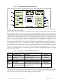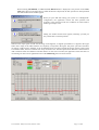
1
XZ170 AGILENT ACQIRIS USER MANUAL FOR SIGNAL ANALYZERS INCLUDING BASE TEST AND FFT SPECTROMETER FIRMWARE Models covered: AC210, AC240 User Manual: Analyzers AC210, AC240 + FFT ZM020190A Rev E June 2007 The information in this document is subject to change without notice and may not be construed in any way as a commitment by Agilent Technologies Inc. While Agilent Technologies makes every effort to ensure the accuracy and contents of the document it assumes no responsibility for any errors that may appear. All software described in the document is furnished under license. The software may only be used and copied in accordance with the terms of license. Instrumentation firmware is thoroughly tested and thought to be functional but it is supplied “as is” with no warranty for specified performance. No responsibility is assumed for the use or the reliability of software, firmware or any equipment that is not supplied by Agilent Technologies Inc. or its affiliated companies. Any versions of this manual which are supplied with a purchased product will be replaced at your request with the latest revision in electronic format. At Agilent Technologies we appreciate and encourage customer input. If you have a suggestion related to the content of this manual or the presentation of information, please contact your local Acqiris representative or Acqiris Technical Support ([email protected]) or come visit our web site at http://www.acqiris.com. Trademarks: product and company names listed are trademarks or trade names of their respective companies Acqiris Headquarters: Acqiris USA: Acqiris Asia-Pacific: Agilent Technologies SA 12, chemin des Aulx CH-1228 Plan-les-Ouates Geneva Switzerland Agilent Technologies Inc. P.O. Box 2203 Monroe, NY 10949 USA Agilent Technologies Australia Pty Ltd 347 Burwood Highway, Forest Hill VIC 3131 Australia Tel: +41 22 884 32 90 Tel: 845 782 6544 Tel: +61 3 9210 2890 Fax: +41 22 884 32 99 Fax: 845 782 4745 Fax: +61 3 9210 5929 © Copyright Agilent Technologies Inc. June 2007 User Manual: Analyzers AC210, AC240 + FFT Page 2 of 69 CONTENTS 1. OUT OF THE BOX ............................................................................................................................................. 6 1.1. Message to the User ....................................................................................................................................... 6 1.2. Using this Manual .......................................................................................................................................... 6 1.3. Conventions Used in This Manual ................................................................................................................. 6 1.4. Disclaimer and Safety .................................................................................................................................... 7 1.5. Warning Regarding Medical Use................................................................................................................... 7 1.6. Packaging and Handling ................................................................................................................................ 7 1.7. Warranty......................................................................................................................................................... 8 1.8. Warranty and Repair Return Procedure, Assistance and Support .................................................................. 8 1.9. System Requirements..................................................................................................................................... 8 1.10. Transport & Shipping................................................................................................................................. 9 1.11. Maintenance ............................................................................................................................................... 9 1.12. Cleaning ..................................................................................................................................................... 9 1.13. Disposal and Recycling............................................................................................................................ 10 2. INSTALLATION ............................................................................................................................................... 11 2.1. IC414 Installation......................................................................................................................................... 11 2.1.1. IC414 Hardware installation hints........................................................................................................ 11 2.1.2. IC414 Windows software installation .................................................................................................. 11 2.2. Installing the Software under Windows ....................................................................................................... 12 2.2.1. Warnings .............................................................................................................................................. 12 2.2.2. Multiple Versions................................................................................................................................. 12 2.2.3. Installation............................................................................................................................................ 12 2.3. Installing the Software for Linux ................................................................................................................. 22 2.3.1. Kernel Mode Driver Compilation ........................................................................................................ 23 2.3.2. Special cases......................................................................................................................................... 24 2.3.3. Environment variables for the Firmware.............................................................................................. 24 2.4. Installing the Hardware ................................................................................................................................ 24 2.5. After Restarting............................................................................................................................................ 25 2.5.1. Windows 2000 ..................................................................................................................................... 25 2.5.2. Windows XP ........................................................................................................................................ 25 2.6. LabVIEW RT............................................................................................................................................... 27 2.7. Installing the IVI-COM/C Driver................................................................................................................. 28 2.8. Distribution for Windows 2000/XP and Linux ............................................................................................ 28 3. PRODUCT DESCRIPTION ............................................................................................................................. 29 3.1. Overview...................................................................................................................................................... 29 3.1.1. Coupling & Impedance ........................................................................................................................ 29 3.1.2. Input Protection.................................................................................................................................... 29 3.1.3. Mezzanine Front-end............................................................................................................................ 29 3.1.4. Bandwidth and Rise Time .................................................................................................................... 29 3.1.5. Input Voltage and Offset ...................................................................................................................... 30 3.1.6. Vertical Resolution............................................................................................................................... 30 3.1.7. DC Accuracy........................................................................................................................................ 30 3.2. Trigger.......................................................................................................................................................... 30 3.2.1. Trigger Source...................................................................................................................................... 30 3.2.2. Trigger Coupling.................................................................................................................................. 30 3.2.3. Trigger Level........................................................................................................................................ 30 3.2.4. Trigger Slope........................................................................................................................................ 31 3.2.5. Window Trigger ................................................................................................................................... 31 3.2.6. HF Trigger............................................................................................................................................ 31 3.2.7. Pre- and Post-Trigger Delay................................................................................................................. 31 3.2.8. Trigger Status ....................................................................................................................................... 31 3.3. Sampling Rate .............................................................................................................................................. 31 3.4. Data Acquisition - Digitizer Mode............................................................................................................... 32 3.5. Data Processing – Analyzer Mode ............................................................................................................... 32 User Manual: Analyzers AC210, AC240 + FFT Page 3 of 69 3.5.1. Data Processing Unit............................................................................................................................ 32 3.5.2. Memory Option.................................................................................................................................... 33 3.5.3. Extended Data Processing Controls ..................................................................................................... 33 3.6. External Clock and Reference...................................................................................................................... 34 3.7. Internal Calibration ...................................................................................................................................... 34 3.8. AC210 Front Panel Inputs and Controls ...................................................................................................... 35 3.9. AC240 Front Panel Inputs and Controls ...................................................................................................... 36 3.10. Physical Specifications............................................................................................................................. 37 3.10.1. Electrical .............................................................................................................................................. 37 3.10.2. Environmental and Physical................................................................................................................. 37 4. FIRMWARE ...................................................................................................................................................... 38 4.1. Base Test Firmware...................................................................................................................................... 38 4.1.1. Architecture of Base Test Firmware..................................................................................................... 39 4.1.2. I/O and Controls of Base Test Firmware.............................................................................................. 39 4.2. FFT Spectrometer Firmware ........................................................................................................................ 40 4.2.1. Architecture of FFT Spectrometer Firmware ....................................................................................... 40 4.2.2. I/O and Controls of FFT Spectrometer Firmware ................................................................................ 41 5. RUNNING THE ACQIRISANALYZERS APPLICATION.......................................................................... 42 5.1. Getting Started with AcqirisAnalyzers......................................................................................................... 42 5.2. Instrument Control Window......................................................................................................................... 42 5.3. Digitizer Control Window............................................................................................................................ 42 5.4. Application Windows & Acquisition Mode................................................................................................. 43 5.5. Base Test Application .................................................................................................................................. 43 5.5.1. Register Tests ....................................................................................................................................... 44 5.5.2. Data Transfer Tests .............................................................................................................................. 44 5.5.3. Memory Tests....................................................................................................................................... 46 5.6. FFT Spectrometer Application..................................................................................................................... 47 5.6.1. Digitizer Setup ..................................................................................................................................... 47 5.6.2. Operation of the FFT Spectrometer...................................................................................................... 48 5.6.3. Power Spectrum Display...................................................................................................................... 50 5.6.4. Monitoring ........................................................................................................................................... 50 6. PROGRAMMING THE FIRMWARE............................................................................................................ 52 6.1. Programming Aspects Common to All AC2x0 Applications ...................................................................... 52 6.1.1. Accessing the DPU Registers............................................................................................................... 52 6.1.2. Register Definitions ............................................................................................................................. 52 6.1.3. Device Initialization ............................................................................................................................. 53 6.1.4. Loading an FPGA Configuration File .................................................................................................. 53 6.1.5. Sequence of Data Processing Operations ............................................................................................. 53 6.1.5.1. 6.1.5.2. 6.1.5.3. 6.1.5.4. 6.1.5.5. 6.1.5.6. Digitizer Configuration......................................................................................................................................54 Starting Data Conversion...................................................................................................................................54 Configuring the Data Processing Unit ...............................................................................................................54 Monitoring.........................................................................................................................................................55 Stopping the DPU Operation .............................................................................................................................55 Stopping the Data Conversion ...........................................................................................................................55 6.1.6. Reading the FPGA Temperature .......................................................................................................... 55 6.2. Registers in the Base Test and FFT firmware .............................................................................................. 56 6.2.1. Register List ......................................................................................................................................... 56 6.2.2. Indirect Addressing .............................................................................................................................. 57 6.2.2.1. 6.2.2.2. Buffer Identifiers in Base Test Firmware ..........................................................................................................58 Buffer Identifiers in FFT Spectrometer Firmware .............................................................................................58 6.3. Programming the FFT Spectrometer Application ........................................................................................ 58 6.3.1. Configuring the Data Processing Unit.................................................................................................. 59 6.3.2. Computing and Loading the (optional) FFT Window.......................................................................... 60 6.3.3. Reading Accumulated Spectra ............................................................................................................. 61 6.3.4. Normalizing the Accumulated Spectra................................................................................................. 62 6.3.4.1. Normalizing the Raw Data ................................................................................................................................62 User Manual: Analyzers AC210, AC240 + FFT Page 4 of 69 6.3.4.2. 6.3.5. 6.3.6. 6.3.7. 6.3.8. 6.3.8.1. 6.3.8.2. 6.3.8.3. 6.3.8.4. 6.3.8.5. 6.3.8.6. 6.3.8.7. 6.3.8.8. 6.3.8.9. 6.3.8.10. 6.3.8.11. 6.3.8.12. 6.3.8.13. 6.3.8.14. Converting the Spectra to dBc Full Scale ..........................................................................................................62 Checking on Overflows........................................................................................................................ 63 Stopping the FFT Spectrometer ........................................................................................................... 63 Synchronizing with other Equipment (e.g. Telescope) ........................................................................ 63 Registers in FFT Spectrometer Firmware ............................................................................................ 64 Indirect Access Port...........................................................................................................................................64 Indirect Address Register ..................................................................................................................................64 Buffer Identifier Register...................................................................................................................................64 AcqirisControl Register.....................................................................................................................................65 Code Protection Register ...................................................................................................................................65 TempMonitor.....................................................................................................................................................65 DEControl Register ...........................................................................................................................................65 Main Control Register .......................................................................................................................................66 Status Register...................................................................................................................................................66 Accumulator Counter ........................................................................................................................................67 FFT Configuration Register...............................................................................................................................67 Front Panel µDB I/O Register ...........................................................................................................................68 Clear Buffer Register.........................................................................................................................................68 Overflow Status Register...................................................................................................................................69 User Manual: Analyzers AC210, AC240 + FFT Page 5 of 69 1. Out of the Box 1.1. Message to the User Congratulations on having purchased an Agilent Technologies Acqiris data conversion product. Acqiris Digitizers /Analyzers are high-speed data acquisition modules designed for capturing high frequency electronic signals. To get the most out of the products we recommend that you read this manual carefully. We trust the product you have purchased will meet with your expectations and provide you with a high quality solution to your data conversion applications. 1.2. Using this Manual The AC240 and AC210 analyzer platforms are dual- and single-channel 6U CompactPCI®/PXITM 1 GS/s per channel digitizers with on-board real-time data processing. The Analyzer functions are dependent on the firmware code loaded into the Data Processing Unit. They are described in this manual throughout the Firmware sections. This guide assumes you are familiar with the operation of a personal computer (PC) running a Windows 2000/XP or other supported operating system. It also assumes you have a basic understanding of the principles of data acquisition using either a waveform digitizer or a digital oscilloscope. The manual is divided into 6 separate sections. To understand the elements of operation for the module it is essential that you carefully read chapters 1-5. Chapter 1 OUT OF THE BOX, describes what to do when you first receive your new Acqiris product. Special attention should be paid to sections on safety, packaging, and product handling. Before installing your product please ensure that your system configuration matches or exceeds the requirements specified. Chapter 2 INSTALLATION, covers elements of installation. Before attempting to use your Acqiris product for actual measurements we strongly recommend that you read all sections of this chapter. Chapter 3 PRODUCT DESCRIPTION, provides a short description of all the functional elements of the AC210 and AC240 Modules. Chapter 4 FIRMWARE, provides a detailed description of the Base Test and FFT Spectrometer firmware including algorithm and implementation aspects. Chapter 5 RUNNING THE ACQIRISANALYZERS APPLICATION describes the operation of the AcqirisAnalyzers application. AcqirisAnalyzers allows interactive operation of the AC240/AC210 from a PC running a Windows 2000/XP operating system. Chapter 6 PROGRAMMING THE FIRMWARE, provides all the information required to write a software application based on the FFT Spectrometer firmware. For information necessary for writing you own software to control Acqiris products you should also refer to the Programmer’s Guide and the Programmer’s Reference Manual. 1.3. Conventions Used in This Manual The following conventions are used in this manual: This icon to the left of text warns that an important point must be observed. WARNING Denotes a warning, which advises you of precautions to take to avoid being electrically shocked. CAUTION Denotes a caution, which advises you of precautions to take to avoid electrical, mechanical, or operational damages. NOTE Denotes a note, which alerts you to important information. Italic text denotes a warning, caution, or note. Bold Italic text is used to emphasize an important point in the text or a note mono text is used for sections of code, programming examples, and operating system commands. User Manual: Analyzers AC210, AC240 + FFT Page 6 of 69 B,KB,MB,GB is for Byte, KiloByte = 1024 bytes, MegaByte = 1024*1024 bytes, GigaByte = 1024*1024*1024 bytes b,Kb,Mb is for bit with multipliers as above. Triggered Denotes a VHDL object. It could be a single- or multi-bit signal or a component or a library name. 0xn..n Denotes a hexadecimal value. 1.4. Disclaimer and Safety The AC Series CompactPCI Analyzer cards have been designed to operate in a CompactPCI/PXI crate. Power for the modules is provided by plugging them into a free slot (refer to the installation procedure). Agilent Technologies does not recommend operation of the AC210 or AC240 outside of a CompactPCI/PXI crate Do not exceed the maximum input voltage rating! The maximum input voltage for 50 Ω input impedance is ±5 V. CAUTION: 1.5. Warning Regarding Medical Use The AC Series CompactPCI Analyzer cards are not designed with components and testing intended to ensure a level of reliability suitable for use in treatment and diagnosis of humans. Applications of these cards involving medical or clinical treatment can create a potential for accidental injury caused by product failure, or by errors on the part of the user. These cards are not intended to be a substitute for any form of established process or equipment used to monitor or safeguard human health and safety in medical treatment. WARNING: The modules discussed in this manual have not been designed for making direct measurements on the human body. Users who connect an Acqiris module to a human body do so at their own risk. 1.6. Packaging and Handling Your Analyzer is shipped with the following components: • A small 3.5” compact disc in an Acqiris paper CD envelope that includes o 10 product user manuals in electronic form (Signal Analyzers, Streamer Analyzers, Family of 8-bit Digitizers, Family of 10-bit Digitizers, Family of 12-bit Digitizers, Family of Averagers, Family of Analyzers, Family of Time Counters, CC10X Family of CompactPCI Crates and CC121 CompactPCI Crate), o 1 Programmer’s Guide and 1 Programmer’s Reference Manual, o device drivers with sample software for different operating systems, environments and languages, o the AcqirisAnalyzers application, a demonstration program for the AC/SC Analyzer products, o the AcqirisLive application, a demonstration program for our digitizer and averager products, o the DemoSSR application, a demonstration program for the Acqiris AP235/AP240 Analyzers, o the DemoAPX01 application, a demonstration program for the Acqiris AP101/AP201 Analyzers, o the DemoTC application, a demonstration program for the Acqiris TC840/TC890 Time Counters, o product data sheets, o full installation procedures for use with Microsoft Windows, National Instruments LabVIEW RT, Wind River VxWorks, IVI-COM/C, and Linux software. • A declaration of conformity • Optional documentation such as a model-dependent document giving Specifications & Characteristics, a Calibration Certificate, or a Performance Verification After carefully unpacking all items, inspect each to ensure there are no signs of visible damage. Also check that all the components received match those listed on the enclosed packing list. Agilent Technologies cannot accept responsibility for missing items unless we are notified promptly of any discrepancies. If any items are found to be missing or are received in a damaged condition please contact the Agilent service center or your local supplier immediately. Retain the box and packing materials for possible inspection and/or reshipment. User Manual: Analyzers AC210, AC240 + FFT Page 7 of 69 1.7. Warranty All Agilent Technologies Acqiris Analyzer products are warranted to operate within specification, assuming normal operation, for a period of three years from the date of shipment. It is recommended that yearly calibration be made in order to verify product performance. All repairs, replacement and spare parts are warranted for a period of 3 months. A 5-year repair warranty is available as an option. Agilent Technologies endeavors to provide leading edge technology that includes the latest concepts in hardware and software design. As such software and firmware used with the products is under continual refinement and improvement. All software and instrument firmware is supplied “as is” with no warranty of any kind. Software and firmware is thoroughly tested and thought to be functional at the time of shipment. At Agilent Technologies’ discretion software and firmware may be revised if a significant operational malfunction is detected. Products supplied but not manufactured by Agilent Technologies are covered solely by the warranty of the original equipment manufacturer. In exercising this warranty, Agilent Technologies will repair or replace any product returned to the Agilent service center, within the warranty period. The warranty covers all defects that are a result of workmanship or materials. This excludes defects that are caused by accident, misuse, neglect, or abnormal operation. The purchaser is responsible for returning the goods to the nearest Agilent service center. This includes transportation costs and insurance. Agilent Technologies will return all warranty repairs with transportation prepaid. 1.8. Warranty and Repair Return Procedure, Assistance and Support Agilent Technologies Inc. acquired Acqiris SA and its product lines in December 2006. Before returning any Agilent Technologies Acqiris product for repair please contact your nearest Agilent Technologies Service Center. You can find information about technical and professional services, product support, and equipment repair and service on the Web, see http://www.agilent.com/find/service (or http://www.agilent.com/ and after selecting your country click on Contact Us). The service center will ask for your name, company, phone number and address, the model and serial numbers of the unit to be repaired, and a brief description of the problem. Before issuing a Service Order they will ask you to communicate with us by phone or eMail so that we can learn as much as needed about the problems observed. If a unit returned under guarantee is found to be working normally and this procedure was not followed we reserve the right to charge you for the work done. For your nearest customer support center contact Acqiris at 1-877-ACQIRIS in the USA, +41 22 884 32 90 in Europe or +61 3 9210 2890 in the Asia-Pacific region. Alternatively, please contact Acqiris Technical Support ([email protected]) or come visit our web site at http://www.acqiris.com. The Agilent Technologies Support Centers can also help redirect you for any questions concerning the installation and operation of your equipment. 1.9. System Requirements In order to obtain reasonable performance from your analyzer, Acqiris products need the following minimum PC System Requirements: Processor: 150 MHz Pentium (higher recommended). Memory: 256 MB RAM. This number is a very rough estimate. Display resolution: At least 1280 x 1024 pixels and 256 colors for use of the AcqirisAnalyzers program is strongly recommended. Operating System: Microsoft Windows 2000/XP including 2003 Server, Wind River VxWorks 5.5.1, and Linux. The following Linux versions have compiled loadable kernel modules: RedHat Enterprise Linux Version 3 - Kernel Version 2.4.21-4.EL RedHat Enterprise Linux Version 3 - Kernel Version 2.4.21-4.ELsmp, Suse Linux 9.2 - Kernel version 2.6.8-24-smp, Debian Sarge 3.1 2.6.8-3-686, Debian 4.0 etch Kernel version 2.6.18-4-686, Scientific Linux 4.4 Kernel version 2.6.9-11.EL). Linux kernel driver source code is available for compilation. Support for Windows 95/98/NT4 is included “as is” since these operating systems are no longer supported by Microsoft. Hard Drive Space: 20 Mbytes Minimum User Manual: Analyzers AC210, AC240 + FFT Page 8 of 69 CD Drive (or any method to copy Acqiris Software installation files from CD to the hard drive such as LAN, floppy drive, etc.) LabVIEW: The Acqiris LabVIEW driver is available for National Instruments LabVIEW versions 7.1or 8.0 LabVIEW RT: The Acqiris LabVIEW RT driver is available for National Instruments LabVIEW RT version 7.1 or higher. The VISA driver must be version 3.0 or higher. MATLAB: The Acqiris MEX interface can be used with MathWorks MATLAB 6.5 or a newer vesion. Visual BASIC: The interface files and examples are available for Microsoft Visual Basic versions 5 or 6 and the interface files only for .NET. Tornado: The example files are useable with Wind River Tornado 2.2.1 1.10. Transport & Shipping CAUTION: Cards can be safely transported in their original shipping packages. DC cards can be transported when properly mounted in a CompactPCI crate. The transport of DP cards mounted in a PC is a more delicate issue. Because of their mass the cards can vibrate loose unless they are properly secured and braced. DP cards held only in the front and on the bottom should not be shipped in their PC. However, properly mounted DP cards with XP103 or XP105 fans can be sufficiently well held; the Adjustable retainer must be used so as to hold the card in place. To package the instrument for shipping: Step Notes 1. Place the instrument in its original packaging materials. • If the original packaging materials are not available, use a professional packaging service. Contact your Agilent Service Center for more information. 2. Surround the instrument with at least 3 to 4 inches (8 to 10 cm) of its original packing material or bubble-pack to prevent the instrument from moving in its shipping container. 3. After wrapping it with packing material, place the instrument in its original shipping container or a strong shipping container that is made of double-walled corrugated cardboard with 159 kg (350 lb) bursting strength. • The shipping container must be large and strong enough to accommodate your instrument and allow at least 3 to 4 inches (8 to 10 cm) on all sides for packing material. 4. Seal the shipping container securely with strong nylon adhesive tape. 5. Mark the shipping container “FRAGILE, HANDLE WITH CARE” to help ensure careful handling. 6. Use the address obtained from your Agilent Technologies Service Center. 7. Retain copies of all shipping papers. CAUTION: Damage can result if the original packaging materials are not used. Packaging materials should be anti-static and cushion the instrument on all sides. NEVER USE STYRENE PELLETS IN ANY SHAPE AS PACKAGING MATERIALS. They do not adequately cushion the instrument or prevent it from moving in the shipping container. Styrene pellets can also cause equipment damage by generating static electricity or by lodging in fan motors. 1.11. Maintenance The cards do not require any maintenance. There are no user serviceable parts inside. A periodic calibration can be obtained on request. 1.12. Cleaning Cleaning procedures consist only of exterior cleaning. Clean the exterior surfaces of the module with a dry lint-free cloth or a soft-bristle brush. If any dirt remains, wipe with a cloth moistened in a mild soap solution. Remove any soap residue by wiping with a cloth moistened with clear water. Do not use abrasive compounds on any parts. User Manual: Analyzers AC210, AC240 + FFT Page 9 of 69 1.13. Disposal and Recycling Electronic equipment should be properly disposed of. Acqiris Digitizers and their accessories must not be thrown out as normal waste. Separate collection is appropriate and may be required by law. User Manual: Analyzers AC210, AC240 + FFT Page 10 of 69 2. Installation This chapter describes how to install the Acqiris hardware and software for Windows 2000/XP, National Instruments LabVIEW RT, Linux, or Wind River VxWorks. NOTE: For a first time installation we strongly recommend installing the software before inserting the hardware into the PC. 2.1. IC414 Installation NOTE: If you are going to install an IC414 interface for the first time and are running Windows 2000/XP you should follow the procedure below before installing the Acqiris hardware. 2.1.1. IC414 Hardware installation hints The PCI-8570/PXI-8570 User's Manual (Rev. 1.00) section 2.5 gives Hardware Installation instructions. CAUTION: Turn off the power of the PC; the PC may have to be unplugged to ensure that the PCI bus has no power available. CAUTION: Touch the antistatic package to a grounded object before removing the card from the package. Electrostatic discharge can damage the card. The standard cable pair provided each have a red connector on one end and a black connector on the other. Therefore the correct connection can be made by plugging the Red connector into the L0Rx socket and the Black connector into the L0Tx socket on the PXI module and the other Red connector into the PCI module socket furthest from the PCI card internal base connector and the Black connector into the next socket. If you intend to use 64-bit 66 MHz transfer to maximize data transfer speed you should cable a “bundled link” using two standard cable pairs and both the L0 and L1 pairs of connectors. You should also make sure that you configure the PXI-8570 M66EN Jumper correctly. 2.1.2. IC414 Windows software installation Linux users do not need to read any further since there is no special software installation. Windows users should have the hardware installed as noted above. This software installation should be done before any Acqiris modules are placed in the CompactPCI crates. This may mean that you have to remove the module from the crate as delivered. The crate should be turned on first followed by the PC. If the cabling and start-up sequence is done correctly there will be no LED illuminated on the PCI unit connected pair and the LED's of the PXI connected pair will be lit. For Windows XP installation, Select the Control Panel under Settings in the Start menu. Then, if you are using the Category View select Printers and Other Hardware. After this, for both Category and Classic views, go to System and then display the Hardware tab to get access to the Driver Signing menu. Since neither the AdLink nor the Acqiris driver has been submitted for Windows Logo testing you must select either the Ignore or Warn action. The resulting menu looks as shown: User Manual: Analyzers AC210, AC240 + FFT Page 11 of 69 The PCI-8570/PXI-8570 User's Manual (Rev. 1.00) section 2.4 contains the software installation instructions. These should be executed before allowing the hardware installation process to look for the driver. If you have an AdLink CD Version 2004A4 or later you can use it; if not you should download the latest driver from the WEB site (http://www.adlinktech.com/). You can then continue with the Hardware Installation. A reboot will then be necessary. At this point the Stargen Fabric PCI Adapter and the Stargen Aruba Fabric-to-PCI Bridge should appear correctly installed under System Devices in the Device Manager. NOTE: If you have an AdLink CD Version 2005A3 or later you can find 8570install.exe in the folder X:\Driver Installation\PXI Platform\PXI Extension\PCI_PXI-8570\Wnt2kxp and the starfab1.inf file in the folder X:\Driver Installation\PXI Platform\PXI Extension\PCI_PXI-8570\Win98. 2.2. Installing the Software under Windows 2.2.1. Warnings If Setup detects a previous installation of Acqiris software on your system, a warning screen will be displayed. It is recommended to exit Setup and uninstall older versions. The installer from software releases prior to Acqiris Software 2.0 installed the Digitizer Driver DLL files into the System directory. These will be removed by Setup. If you wish to keep the old installation on your system, you should exit Setup, and move all Acqiris driver files (acqiris*, acqrs* and acqir*) to some archive directory. The DLL files will be installed into the bin subdirectory of the Acqiris software root, and the corresponding path will be added to the PATH environment variable. 2.2.2. Multiple Versions With the software installation from Acqiris Software 2.0 (or above), it is possible to keep multiple versions on the same system, but you must specify a different root directory (i.e. Install Folder). If you keep the same directory, Setup will overwrite your previous installation. To go back to a previous version, you must change the PATH environment variable and reinstall the Kernel driver. Under Windows 2000/XP: 1. Copy the SYS file from <old_AcqirisSoftware_root>\bin\kernel to the Windows\System32\drivers directory. 2. Change the AcqirisDxRoot, AcqirisDxDir and PATH environment variables to the old root. 3. Reboot the computer. 2.2.3. Installation Before installing the Acqiris hardware, you should complete the following steps to install the software for Windows 2000/XP. NOTE: You will need administrator privileges to complete the software installation under Windows 2000/XP. 1. Insert the Acqiris Software CD into the CD-ROM drive of your computer. If the Autorun program does not start automatically (Autoplay disabled), you can start it manually, or navigate to the AcqirisSoftware\Windows folder in order to display the files included. 2. Choose Install AcqirisSoftware for Windows 2000/XP (or run Setup.exe from AcqirisSoftware\Windows folder). After several seconds for initialization the following screen will appear. User Manual: Analyzers AC210, AC240 + FFT Page 12 of 69 the 3. To proceed with the installation click “Next”. The following screen will be shown. 4. Please enter your user information and click “Next” to continue. If the program finds that there is still Acqiris software installed on your machine a warning panel (not shown) will appear. Otherwise, the next screen shows: User Manual: Analyzers AC210, AC240 + FFT Page 13 of 69 5. Pick the desired combination of module families and click "Next" to continue. 6. The screen above will normally allow the documentation to be installed. Remove the check from the box if you do not want online access to the manuals. 7. The next screen allows you to enable LabVIEW RT and/or Wind River VxWorks support. By default there will be none but if desired you can install any of them together with Windows support or without Windows support. Click “Next” to continue. User Manual: Analyzers AC210, AC240 + FFT Page 14 of 69 8. The screen below asks for the desired installation type. After having made your choice Click “Next” to continue. 9. If you chose the Custom installation, the following screen will let you select each package individually. Note that the space indicated for LabVIEW, Firmware and UserManual packages is incorrect. The correct values are 4.1 MB, 21 MB, and 27 MB respectively. User Manual: Analyzers AC210, AC240 + FFT Page 15 of 69 10. If MATLAB is installed on your machine, you will be asked to point the installer to the MATLAB root directory. You should do this if you want the installer to modify the standard startup.m file to incorporate the Acqiris adaptor. 11. Now that the elements of the installation have all been decided you will be prompted for the installation folder. This will be the root directory of the Acqiris software installation. If User Manuals (27 MB) and Firmware (21 MB) are loaded more space than indicated here will be required on the drive. For the case of a Tornado 2.2 installation the folder name should not contain any spaces. 12. Furthermore, you should give a name to the shortcut folder. This is the menu entry under Start → Programs where you will find the shortcuts for AcqirisLive, manual(s), etc. User Manual: Analyzers AC210, AC240 + FFT Page 16 of 69 13. If you have enabled the installation of 12-bit Digitizers, Averagers, or Analyzers, the next screen lets you change the name of the directory where the FPGA firmware will be installed. 14. AcqirisLive needs the LabWindows/CVI 7.0 Run-Time Engine to run. If Setup has detected that a LabWindows/CVI Run-Time Engine is already installed on your system, it will ask you if you would like to install it locally for AcqirisLive anyway. If you are not sure about the version of the CVI Run-Time Engine on your system, it is recommended to install it locally. Click “Next” to continue. User Manual: Analyzers AC210, AC240 + FFT Page 17 of 69 15. Depending on the install type, you may be asked which LabVIEW version format you want for the LabVIEW files. Select the appropriate format and click “Next” to continue. 16. A summary will be shown to allow you to check what you have asked for User Manual: Analyzers AC210, AC240 + FFT Page 18 of 69 17. You are now ready to install. You may still go back to any previous screen to modify your selection. Click “Install” when ready. 18. Setup will now copy the files and make the necessary changes to your system. When done, an information screen will be displayed. Please read this carefully. User Manual: Analyzers AC210, AC240 + FFT Page 19 of 69 19. Registration of your installation will help us provide you with better support. You will also be notified of updates and upgrades. All information submitted to us will be treated confidentially and never be disclosed outside the company. User Manual: Analyzers AC210, AC240 + FFT Page 20 of 69 20. Setup will prepare a registration e-mail in your e-mail client application upon termination of the setup procedure. You can then decide whether or not you wish to send it. You may also add comments. Uncheck the box if you do not want to register your installation. 21. Click “Finish”. The software installation is now complete. 22. You can now either accept the suggestion to restart the computer or you should shutdown your computer and proceed with the hardware installation. User Manual: Analyzers AC210, AC240 + FFT Page 21 of 69 2.3. Installing the Software for Linux The Acqiris Software is ready to install and run on Linux systems with any of the following: RedHat Enterprise Linux Version 3 - Kernel Version 2.4.21-4.EL RedHat Enterprise Linux Version 3 - Kernel Version 2.4.21-4.ELsmp, Suse Linux 9.2 - Kernel version 2.6.8-24-smp, Debian Sarge 3.1 2.6.8-3-686, Debian 4.0 etch Kernel version 2.6.18-4-686, Scientific Linux 4.4 Kernel version 2.6.9-11.EL) The following tar files exist with the driver and library compiled with the GNU gcc version shown: AcqirisLinux-3.1a-gcc-3.3.tar.gz - compiled under Suse 9.2 with GNU gcc 3.3. AcqirisLinux-3.1a-gcc-3.4.tar.gz - compiled under SL 4.4 with GNU gcc 3.4. AcqirisLinux-3.1a-gcc-4.1.tar.gz - compiled under Debian etch with GNU gcc 4.1. The Kernel Driver source code is available for recompilation for users with other Linux systems. The appropriate tar file should be copied to a local directory (e.g. your home directory) and then unpacked by using the following command tar xzf AcqirisLinux-3.1a-gcc-X.x.tar.gz The resulting directory AcqirisLinux contains an install script drv-install and a graphical Demo program demo/AcqirisDemo. Before installing the driver you have to put the correct version of the Kernel mode driver into acqirisPCI.o. Type cd AcqirisLinux/lib/modules and either cp acqrsPCI.o[.n] acqrsPCI.o (Linux kernel 2.4) or cp acqrsPCI.ko[.n] acqrsPCI.ko (Linux kernel 2.6) where [.n] is the running version of the Linux kernel. This can be obtained by running the command uname -r The following versions exist: User Manual: Analyzers AC210, AC240 + FFT Page 22 of 69 acqrsPCI.o.2.4.21-4.EL acqrsPCI.ko.2.6.8-3-686 acqrsPCI.ko.2.6.8-24-smp acqrsPCI.ko.2.6.9-11.EL acqrsPCI.ko.2.6.18-4-686 for Red Hat Enterprise Linux version 3 for Debian 3.1 'sarge' for Suse 9.2 for Scientific Linux 4.4 for Debian 4.0 'etch' To install the driver and the load script to the system, you have to get super user privileges and execute the driver install script by typing, cd AcqirisLinux ./drv-install add You can check that the driver is loaded properly with lsmod or dmesg. The drv-install script has the following additional functionality: drv-install rem to remove the driver and load script drv-install res to restart the driver If you intend to use an Averager, an Analyzer, or a 12-Bit Digitizer you must install the Firmware .bit files. You can either copy them from the Firmware directory of the CD-ROM or download them from our WEB site. They should be placed in the Firmware subdirectory of AcqirisLinux. In the case of the CD-ROM, this can be done by continuing the above command sequence with the following: cp /mnt/CDRom/Firmware/*.bit Firmware/ 2.3.1. Kernel Mode Driver Compilation For some special kernels, for example SMP, the kernel mode driver will have to be recompiled on the target system. All files needed to compile a new kernel mode driver are in AcqirisLinux/linuxdriverpci for Kernel 2.4 or in AcqirisLinux/linux2.6driverpci for Kernel 2.6 The makefile can be used for compilation under a standard compatible distribution. To compile the driver, the kernel header files need to be installed. Furthermore, depending on the Linux distribution, the kernel source files may need to be installed. The makefile will try to guess where they are located. If it fails, see instructions inside the makefile itself to specify manually where these kernel header files are located. To compile a new kernel under linux-2.4, issue the following commands: cd linuxdriverpci make clean to remove all *.o files in AcqirisLinux/linuxdriverpci. make to generate a new kernel mode driver acqrsPCI.o and also copy it to the directory AcqirisLinux/lib/modules where the install script (drv_install) can access it. drv_install rem to remove the previous installed kernel mode driver. drv_install add to install the new driver. To compile a new kernel under linux-2.6, issue the following commands: cd linux2.6driverpci make clean all to generate a new kernel mode driver acqrsPCI.ko from scratch. make install to copy the kernel module where it should reside. Note that this version of the loadable kernel module had been tested on Linux kernel versions up to 2.6.18. However, starting with kernel 2.6.17, a few kernel functions relating to the device classes are no longer available to proprietary modules. Thus automatic creation of the /dev/acqrsPCI node has to be done manually in the /etc/rc.local file. For Debian users, in order to compile the kernel module on a system, a few packages that match the current kernelimage must be installed. For instance, on a Debian 3.1 sarge system 686 the required packages are: kernel-image-2.6-686 kernel-image-2.6.8-3-686 kernel-headers-2.6-686 kernel-headers-2.6.8-3 kernel-headers-2.6.8-3-686 kernel-kbuild-2.6-3 User Manual: Analyzers AC210, AC240 + FFT Page 23 of 69 2.3.2. Special cases If you are running a Linux distribution that doesn’t use the standard paths for the load scripts, you can load the driver with the command cd AcqirisLinux ./drv-install load Copy the driver to the module directory as follows: cp lib/modules/acqrsPCI.o[.n] /lib/modules/{kv}/ACQIRIS/acqrsPCI.o where [.n] is the optional designation of the desired version of the acqrsPCI driver as given above and {kv} is the appropriate system kernel version (obtained with uname -r, i.e. 2.4.20). Then add the following command to /etc/rc.local. /sbin/insmod –f /lib/modules//{kv}/ACQIRIS/acqrsPCI.o For systems using udev (the dynamic /dev/ hierarchy) it may be convenient to automatically create the /dev/acqrsPCI node at boot. To do this, add the following command to the /etc/rc.local file: /sbin/mknod -m 666 /dev/acqrsPCI c 124 0 2.3.3. Environment variables for the Firmware Automatic loading of the firmware needed by 12-bit, analyzer, and averager modules relies on the environment variable AcqirisDxDir pointing to the directory containing the file AqDrv4.ini which in turn points to the directory containing the Firmware .bit files. Therefore, assuming that your Firmware is in /usr/local/AcqirisLinux/Firmware and that AqDrv4.ini is in /usr/local/AcqirisLinux/demo then you must edit AqDrv4.ini so that it contains the line fpgaPath=/usr/local/AcqirisLinux/Firmware Then, if your shell is csh or tcsh modify the /etc/csh.login file to contain the line setenv AcqirisDxDir /usr/local/AcqirisLinux/demo or, if your shell is bash, ksh, zsh or sh, modify the /etc/profile file to contain the lines AcqirisDxDir=/usr/local/AcqirisLinux/demo export AcqirisDxDir 2.4. 1. Installing the Hardware Turn off the power of the PC and the crate in the case of a CompactPCI module. CAUTION: For PCI modules the PC may have to be unplugged to ensure that the PCI bus has no power available. However, CompactPCI crates can be left plugged in since this ensures proper grounding. CAUTION: Touch the antistatic package to a grounded object before removing the card from the package. Electrostatic discharge can damage the card. 2. Module in a PC: open the PC, identify a free PCI slot and carefully insert the DP Series card into it. Be sure to ground yourself by touching the grounded PC frame and avoid touching any components on the DP Series card. Make sure that the grounding of the card’s mounting bracket to the back panel rail of the computer is done correctly. If present make sure that the fan's adjustable retainer is correctly positioned and tightened for mechanical support. Close the PC. Module in a CompactPCI crate: Follow the instructions of the crate manufacturer to insert the DC Series card into a free 6U CompactPCI peripheral slot. Be sure to ground yourself by touching the grounded crate and avoid touching any components on the DC Series card. Be sure to tighten both front panel mounting screws to lock the module into place and insure proper grounding of the frame. NOTE: To ensure the best possible performance, users of Acqiris CC121 Crates with ASBus systems should respect the module placement rules to be found in the Acqiris CC121 CompactPCI Crate User Manual. PCI Bus extension module in a PC: Consult the manufacturer's documentation for any special instructions. Open the PC, identify a free PCI slot and carefully insert the card into it. Be sure to ground yourself by touching the grounded PC frame and avoid touching any components on the card. Make sure that the grounding of the card’s mounting bracket to the back panel rail of the computer is done correctly. Close the PC. Connect the module to the CompactPCI crate controller. User Manual: Analyzers AC210, AC240 + FFT Page 24 of 69 3. Turn on the power of the crate(s), if present, and then the PC and start the operating system. NOTE: Acqiris Digitizers are equipped with a LED. If this LED is not glowing orange or red when the power is applied there is a severe problem. Either the module is broken or the necessary voltages for its use are not available. NOTE: For proper system operation when using the IC200, IC414, or other PCI extension interface to connect a CC10X crate to a remote PC, the crate must be powered on before the PC in order for the PC BIOS to recognize the presence of the CompactPCI crate. 4. Devices that were installed using a previous version of Acqiris Software the instruments in these logical positions will still appear as Unknown Devices. This can be changed to the new Acqiris type category with the Grey Diamond icon by Uninstalling the device and then Installing again. Instructions on this procedure can be found in the ReadMe.txt file in the manuals folder of your Acqiris Software installation. 2.5. After Restarting 2.5.1. Windows 2000 Under Windows 2000, you must login with administrator privileges after the first boot following the hardware installation; the Plug&Play system must have the appropriate privileges to be able to complete your hardware installation successfully. After a successful hardware installation, you will be able to use your Acqiris Digitizer(s) with normal privileges. At the first boot following the hardware installation, Windows will detect the new hardware and will install the devices automatically. The following image will appear. NOTE: In some systems an application program (such as AcqirisLive) will not yet work correctly at this point. One additional boot cycle may be needed if this is the first time that a hardware board is being installed. 2.5.2. Windows XP Under Windows XP, you must login with administrator privileges after the first boot following the hardware installation; the Plug&Play system must have the appropriate privileges to be able to complete your hardware installation successfully. After a successful hardware installation, you will be able to use your Acqiris Digitizer(s) with normal privileges. If you login with administrator privileges after the first boot following the hardware installation, Windows will detect the new hardware and start the “Found New Hardware Wizard” after a few seconds. User Manual: Analyzers AC210, AC240 + FFT Page 25 of 69 To proceed with the installation click "No, not this time" and then “Next”. The following window will appear: To proceed with the installation click “Next”. You should then see User Manual: Analyzers AC210, AC240 + FFT Page 26 of 69 and then NOTE: In some systems an application program (such as AcqirisLive) will not yet work correctly at this point. One additional boot cycle may be needed if this is the first time that a hardware board is being installed. 2.6. LabVIEW RT During program development you can choose whether you use LabVIEW or LabVIEW RT compatible libraries by switching the version present in National Instruments\LabVIEW m.n\instr.lib\. This swap can be facilitated by using the Install VI library for LabVIEW or LabVIEW Real-Time shortcut available in the Shortcut folder under Start → Programs. User Manual: Analyzers AC210, AC240 + FFT Page 27 of 69 There is only one Acqiris Driver. It supports all Acqiris Instruments. The instructions below concern LabVIEW RT as used in NI PXI processors. The Aq_RT.inf and AqRT_4.ini files must be uploaded to the target. To do this, • start the MAX application, • right click on the target • select file transfer • select the Aq_RT.inf file on your host machine and upload ('To Remote') to the LabVIEW RT working directory (/NI-RT/system) on the target • select the Aq_RT.ini file on your host machine and upload ('To Remote') to the LabVIEW RT working directory (/NI-RT/system) giving it the name AqDrv4.ini For Acqiris modules which need FPGA files you should, • create the folder \firmware in the /NI-RT/system directory using the file transfer application • select the FPGA files (from <AcqirisDxRoot>\Firmware) you want to copy to the target and upload them into the firmware directory Restart the target after finishing the file transfers. Restart the MAX Explorer and you should have Acqiris digitizers detected in your PXI system. 2.7. Installing the IVI-COM/C Driver Please install Acqiris Software for Windows first. Then the Acqiris Software CD Autorun program gives access to two installers: IVI Shared Components 1.4 IVI-COM/C IviAqD1 driver These must be installed in the order shown above. For more information you can then consult the Readme.txt file in the IVI\Drivers\IviAqD1 folder or the documentation through the program shortcut present under Ivi/IviAqD1. 2.8. Distribution for Windows 2000/XP and Linux The manuals/ReadMe.txt file contains a list of files to be found after a complete installation of Acqiris Software on Windows systems. Similarly the ReadMeLinux file gives the list of files corresponding to that installation. User Manual: Analyzers AC210, AC240 + FFT Page 28 of 69 3. Product Description 3.1. Overview The AC Series are powerful analyzer platforms based on a single-channel (AC210) or dual channel (AC240) 1 GS/s per channel, 8-bit CompactPCI digitizer with on-board real-time data processing implemented with the aid of a large field-programmable gate array (FPGA). The AC Series Architecture offers a convenient way to implement user defined data processing algorithms with data rates of up to 2 GS/s. It provides external processing control through dedicated connectors and visual reference by means of two front-panel LEDs. Key Features • Dual-Channel Performance with Interleave – The AC240 offers dual-channel synchronicity for I/Q acquisitions with up to 1 GS/s sample rate. Interleaved single-channel mode up to 2 GS/s on either input is software selectable. The AC210 provides a single input channel with a sample rate of up to 1 GS/s. • On-board reconfigurable Data Processing Unit (DPU) – The AC Series analyzer platform can easily be reconfigured to perform a variety of user-defined on-board real-time signal processing tasks on the digitized signals. The on-board FPGA is capable of executing multiplications in less than 5 ns and offers more than 74,000 logic cells, up to 7 Mbits of on-chip RAM, and 328 dedicated 18-bit x 18-bit multipliers with 36-bit results. • Optional external Processing Memory – As an option, the AC Series can be equipped with additional memory to extend the processing capability of the DPU. The P512M Memory option offers two independent banks of 256 MB of DDR333-SDRAM and a 1 MB dual-port SRAM. • Front-panel I/O Connectors and Controls for real-time data processing control (DPU Ctrl2) – It provides several front-panel connectors for real-time control of the DPU. The function of these connectors and LEDs is user defined through the implemented firmware. 3.1.1. Coupling & Impedance Each channel has a 50 Ω signal input BNC connector giving high quality termination with better than ± 1% precision. It is ideally suited for use with 50 Ω transmission lines. Both AC and DC coupling modes are available. The AC mode couples signals capacitively thus removing the input signal’s DC component and filtering out any signal component below 32 Hz. DC mode allows all signal components to be passed through to the digitizer. 3.1.2. Input Protection The input amplifiers are fully protected against over-voltage signals. Input signals up to ±5 V DC at 50 Ω, can be input without damaging the front-end electronics. 3.1.3. Mezzanine Front-end The front-end electronics are all mounted on a removable mezzanine card. In the event of accidental damage, or as components fatigue over time (e.g. relays in high duty cycle automated testing applications), the mezzanine card allows for fast and efficient replacement. 3.1.4. Bandwidth and Rise Time The bandwidth specification indicates the frequency at which an input signal will be attenuated by 3 dB (approximately 30% loss of amplitude). The bandwidth also affects the minimum rise and fall times that can be passed through the front-end electronics. A pulse with a very sharp edge will be observed to have a minimum rise time (τmin) determined by the front-end electronics. In general a pulse with a given 10-90% rise time (τ10-90real) will be observed with a slower value given by: τ10-902 = τ10-90real2 + τmin2 where τmin (ns) ≈ 0.35 (GHz-ns) / BW (GHz) If desired, a hardware bandwidth limiter at 20, 200 or 700 MHz can be selected. User Manual: Analyzers AC210, AC240 + FFT Page 29 of 69 Model Agilent # Bandwidth into 50 Ω AC210, 1GHz Minimum Rise Time 0.35 ns AC240 ≈ U1080A 3.1.5. Input Voltage and Offset The input channel provides a fully programmable amplifier with variable input voltage and offset. Full Scale (FS) input voltages are selectable from 50 mV to 5 V in a 1, 2, 5 sequence. Care should be taken to select an input voltage range that will allow the signal to be recorded using as much dynamic range of the digitizer as possible. The variable offset is programmable in the range of ± 2 V, in the FS ranges 50 to 500 mV, and ± 20 V, in the FS ranges 1 V to 5 V. The raw 8 bit ADC data values are in the range [-128,+127] with the first and last values reserved for underflow and overflow respectively. The midpoint value, 0, of the range corresponds to the negative of the offset voltage. Thus the Full Scale Range (FSR) goes from –Offset Voltage – (FS/2) to –Offset Voltage + (FS/2) Signals going outside of the FSR will be clipped and data values for the clipped portion of a signal should be regarded as erroneous. 3.1.6. Vertical Resolution The AC Series Analyzers use an ADC system with 8 bits of vertical resolution (256 levels). The dynamic range of the ADC covers the Full Scale (FS) of the Input Voltage setting. For example, if the Input Voltage is set to 500 mV then the ADC resolution is equivalent to 1.95 mV. Analyzers use low noise front-end electronics in order to ensure a good signal to noise ratio. To obtain the best dynamic range from the ADC care should be taken to ensure that the input signal varies over more than 50% of the Input Voltage Full Scale (FS) setting. The highest and lowest levels of the ADC correspond to underflow and overflow conditions. 3.1.7. DC Accuracy DC voltage accuracy is better than ± 2% (± 1% typical) of the input voltage full-scale. The differential linearity is better than ± 0.9 LSB 3.2. Trigger In normal digitizer operation, the trigger signal stops the data acquisition, typically somewhat delayed, depending on the user-specified delay value. When the card is operated as a continuous data analyzer, the trigger signal is routed to the DPU where it is used as an indicator of the time region of interest. However, it does not stop the acquisition. 3.2.1. Trigger Source The trigger source can be a signal applied to either the Input Channel (for internal triggering) or the External Trigger Input. The modules provide a front panel BNC External Trigger Input. The External Input provides a fully functional trigger circuit with a fixed 50 Ω termination impedance, as well as selectable level and slope. It has the same BW limiter selections as can be found for the input channel. The user can choose the external trigger Full Scale from the set of values 0.5, 1.0, 2.0 or 5.0 V. A ±5 V limit on trigger signals should be respected, although somewhat higher voltages for short time periods will not damage the unit. 3.2.2. Trigger Coupling Trigger coupling is used to select the coupling mode applied to the input of the trigger circuitry. Modes available include AC LF Reject, HF Reject, and DC. The AC LF Reject mode couples signals capacitively and removes the input signal's DC component and frequencies below 50 Hz. DC mode allows all signal components to be passed through to the trigger circuit. The HF Reject mode removes signal components above 50 kHz. 3.2.3. Trigger Level The trigger level specifies the voltage at which the selected trigger source will produce a valid trigger. The trigger level is defined as a set voltage. Using the internal trigger with DC coupling, the level is set with respect to the midpoint voltage (Vm= – Offset voltage) of the digitizer’s vertical scale. Internal trigger level settings must be within User Manual: Analyzers AC210, AC240 + FFT Page 30 of 69 Vm ± 0.5 FS, where FS is the channel or External Full Scale. All trigger circuits have sensitivity levels that must be exceeded in order for reliable triggering to occur. Trigger levels are also adjustable when using AC coupling. AC Series digitizers will trigger on signals with a peak-peak amplitude > 15% FS from DC to their bandwidth limit. 3.2.4. Trigger Slope The trigger slope defines the direction of the signal that will be used to initiate the acquisition when it passes through the specified trigger level. Positive slope indicates that the signal is transitioning from a lower voltage to a higher voltage. Negative slope indicates the signal is transitioning from a higher voltage to a lower voltage. 3.2.5. Window Trigger The AC Series digitizers implement a Window trigger. Two trigger level thresholds are used to define the desired range. The trigger can then be chosen to occur either when the signal exits or enters the window range. This mode can be thought of as the appropriate OR of two edge triggers of opposite slope. 3.2.6. HF Trigger The AC Series digitizers implement an HF trigger that allows triggers to be reliably accepted at rates above ∼ 1 GHz. In this mode, triggers occur on every fourth positive edge. The window trigger is not available in this mode. 3.2.7. Pre- and Post-Trigger Delay The pre- and post-trigger counters are only used in normal digitizer mode. When the card is operated as a continuous data analyzer, no acquisition trigger is required. The pre- and post-trigger counters are therefore ignored at this level. To increase trigger flexibility a pre- or post-trigger delay can be applied to the trigger position. The amount of pre-trigger delay can be adjusted between 0 and 100% of the acquisition time window (i.e. sampling interval x number of samples), whereas the post-trigger delay can be adjusted between 0 and 200 million samples. Pre- or post-trigger delays are just different aspects of the same trigger positioning parameter: • The condition of 100% pre-trigger indicates that all data points are acquired prior to the trigger, i.e. the trigger point is at the end of the acquired waveform. • The condition of 0% pre-trigger (which is identical to a post-trigger of 0) indicates that all data points are acquired immediately after the trigger, i.e. the trigger point is at the beginning of the acquired waveform. • The condition of a non-zero post-trigger delay indicates that the data points are acquired after the trigger occurs, at a time that corresponds to the post-trigger delay, i.e. the trigger point is before the acquired waveform. The digitizer hardware accepts pre- and post-trigger adjustments in increments of 16 samples. By definition posttrigger settings are a positive number and pre-trigger settings are a negative number. Thus it is only natural that the software drivers treat pre- and post-trigger delays as a single parameter in seconds that can vary between –nbrSamples * samplingInterval (100% pre-trigger) and +maxPostTrigSamples * samplingInterval (max post-trigger of 200M samples). Since the Acqiris software drivers provide very accurate trigger position information upon waveform readout, the accepted resolution of the user-requested pre-/post-trigger delay is much better than 16 samples. For more details, refer to the Programmer’s Reference Manual. 3.2.8. Trigger Status The front panel includes a tri-color LED indicator to show the status of the trigger for normal digitizer mode. This LED indicator is located near the TRIGGER IN BNC Connector. When the LED is green it indicates the trigger is armed and waiting for a valid trigger to occur. Red indicates that the trigger has occurred, the acquisition is complete, and the data is waiting to be read out. The user can override the default functions and program the LED color in an application-specific manner. When the AC Series are used as an analyzer this LED is always green when the acquisition is continuously running. 3.3. Sampling Rate All Acqiris digitizers contain an analog-to-digital conversion (ADC) system that can sample waveforms, in a real time sampling mode, at rates from the maximum allowed rate down to 100 S/s (10 ms per point). The sampling rate can be programmed and is selectable in a 1, 2, 2.5, 4, 5 sequence (i.e. 1 MS/s, 2 MS/s, 2.5 MS/s, 4 MS/s, 5 MS/s, 10 MS/s, etc.). The maximum sampling rate shown above sometimes exploits the possibility of combining channels. The AC210 can sample up to 1 GS/s and the AC240 up to 2 GS/s. The data of all of the active channels is acquired User Manual: Analyzers AC210, AC240 + FFT Page 31 of 69 synchronously; all of the ADC’s are acquiring data at the same time, to within a small fraction of the maximum sampling rate. 3.4. Data Acquisition - Digitizer Mode Data from the ADC are stored in on-board acquisition memory. The amount of memory in use for acquisition can be programmed and is selectable from 2 points to 128 Kpoints, the full amount of acquisition memory available. For technical reasons, a certain memory “overhead” is required for each waveform, reducing the available memory by a small amount. In order to simplify programming, an interface function recommends the best sampling rate and the maximum possible number of data points, taking into account the available memory, the requested time window, the number of segments (in Sequence mode), as well as the required memory overhead. The Time Base Range defines the time period over which data is being acquired. For example, the AC210 in the digitizer mode has an acquisition memory of just under 128 Kpoints and maximum sampling rate of 1 GS/s. Thus, at the maximum sampling rate, the digitizer can record a signal over a time period of up to 130 μs (128 Kpoints * 1 ns/point). The time base range can be adjusted by varying the amount of acquisition memory or the sampling rate of the digitizer. 3.5. Data Processing – Analyzer Mode Data from the ADC are continuously streamed through the data demultiplexer (MAC) to the on-board Data Processing Unit. The Data Processing Unit of the AC Series is implemented as a large field-programmable gate array (FPGA) with optional external memory. The figure below presents the Data Processing hardware environment and some of the basic blocks used to interface them. 3.5.1. Data Processing Unit The Data Processing Unit is well suited for many data processing schemes. It is implemented as a powerfull FPGA, the Xilinx Virtex II Pro XC2VP70-6FF1517 that provides up to two embedded PowerPCs, 328 18-bit x 18-bit multipliers, and 328 block RAMs. The main features are summarized in the table below. Please refer to http://www.xilinx.com for the latest information about this device. Resources Qty Logic cells 66176 Block RAM 328 Description / Comment 1 Logic cell has 1x (4 Input LUT + Flip-Flop + Carry Logic) Instances of block RAM, 18 kbits each User Manual: Analyzers AC210, AC240 + FFT Page 32 of 69 Multiplier 328 18-bit x18-bit multipliers DCM 8 Digital clock manager including frequency synthesis and phase shifting features. Frequency up to 420 MHz. BUFG 16 Global Clock Buffer Rocket IO 16 Not connected PowerPC 2 No support from Acqiris In addition, the P512MB Memory option can improve the processing capability. The Analyzer functions are completely dependent on the firmware downloaded into the Data Processing Unit. The application-specific firmware available for the AC2x0 Series is described in chapter 4 FIRMWARE. As an option, a FDK (Firmware Development Kit) for the Acqiris AC2x0 series enables users to develop and integrate user-specific data processing algorithms. The FDK reduces the development effort by providing a set of cores that interface to the underlying hardware resources. Please refer to the FDK User Manual for more information. 3.5.2. Memory Option The external DPU memory option consists of: • 2 banks of 256MB of DDR333 SDRAM with a throughput of up to 2 GB/s per bank. • 1 MB of dual-port SRAM with a read/write throughput of up to 1 GB/s per port. Each DDR bank is built around four 512Mbit DDR-SDRAM devices that are organized as 8M x 16bits x 4 banks. Data are synchronously transferred on a 64-bit wide bus on each edge of a 166.67 MHz clock. A DDR Controller that is able to sustain continuous burst reading or writing at a data rate of up to 2 GB/s is provided as part of the FDK. The Dual Port Memory is built around two 4Mbit Dual Port SRAM organized as 128K x 36 bits. Data are synchronously transferred on a 64-bit wide bus on each port using a clock at up to 166.67 MHz. A Dual Port Controller that is able to sustain continuous simultaneous burst reading and writing at a data rate of up to 1 GB/s is provided as part of the FDK. 3.5.3. Extended Data Processing Controls The AC Series provides several front-panel connectors for real-time control of the DPU. The function of these connectors and LEDs is user defined through the implemented firmware. Two front-panel digital I/O MMCX-type connectors (I/O P1 & P2) are dedicated to the direct control of the data processing unit. These signals are 3.3 V compatible CMOS. Each digital I/O can independently be configured either as an input or as an output. The figure below shows the equivalent schematic of one I/O Px interface. The series resistor value is 50 Ω. I/O Px and I/O CTRx signals are connected to the Data Processing Unit. A third MMCX front-panel coaxial connector (ANL Out) is an analog output signal whose voltage is driven by a 16bit on-board serial DAC. This analog signal can be used in simple control systems. The voltage range of that signal is –5V to +5V. The typical settling time (full scale range) is 1µs. A front-panel μDB-15 connector (I/O EXT) provides fourteen bi-directional direct lines to the DPU that can be used as seven differential pairs or as fourteen closely coupled single ended lines. Please note that these lines must use 2.5V signaling logic standards. User Manual: Analyzers AC210, AC240 + FFT Page 33 of 69 CAUTION: Do not exceed the maximum input voltage rating! The maximum input voltage for µDB-15 Connector is 2.6 V. The figure below shows the pinout of the μDB-15 connector. Pin 15 is connected to the electrical ground. The table below shows the pinout allocation of the I/O EXT connector. Each DPxn/DPxp pair refers to two lines routed towards the data processing unit as a differential pair. Pin Allocation 1-2 DP6n – DP6p 3-4 DP5p – DP5n 5-6 DP4p – DP4n 7-8 DP0p – DP0n 9-10 DP3p – DP3n 11-12 DP2p – DP2n 13-14 DP1p – DP1n 15 GND Finally, two LEDs (L1 & L2) provide a visual reference. Each LED is independently driven by the Data Processing Unit and displays one of the four following colors (Black or switched off, Red, Green, or Orange). 3.6. External Clock and Reference For applications where the user wants to replace the internal clock of the digitizer in order to drive the ADC with an external source, an External Clock or Reference signal input is available. The Clock or Reference signals can be entered into the digitizer via the MMCX CLK IN connector on the front panel. When using an External Clock, the user must ensure that the input signal has a frequency between 10 MHz and 2 GHz, and a minimum amplitude of at least 1 V, peak to peak, into 50 Ω. The External Clock allows the digitizer to make a voltage measurement whenever the clock signal passes through a predefined threshold. However, it should be noted that when 2 channels are being used the maximum Sampling Rate is half of the External Clock Frequency in the Continuous mode and in this case the Start/Stop mode is to be preferred. The threshold range is variable and user selectable between ± 2 V. The signals should not exceed ±5 V amplitude. For applications that require greater timing precision and stability than is obtainable from the internal clock, a 10 MHz Reference signal can be used. The amplitude and threshold conditions, for an External Reference, are the same as for the External Clock. If phase synchronization between several digitizers is required, the reference signal should be applied to all of them. 3.7. Internal Calibration The software drivers supplied include calibration functions for the timing, gain, and offset settings, which can be executed upon user request. The digitizers are never calibrated in an “automatic” way, i.e. as a side effect of another operation. This ensures that programmers have full control of all calibrations performed through software in order to maintain proper event synchronization within automated test applications. The AC2x0 includes a high precision voltage source and a 16-bit DAC, used to determine the input voltage and offset calibration. For accurate time and voltage measurements it is recommended to perform a calibration once the module has attained a stable operating temperature (usually reached with a few minutes after power on). Further calibration should not be necessary unless temperature variations occur. User Manual: Analyzers AC210, AC240 + FFT Page 34 of 69 3.8. AC210 Front Panel Inputs and Controls Name Generic Function Comments L1 LED Status (*) Firmware Dependent LED L1 L2 LED Status (*) Firmware Dependent LED L2 ANL Out Analog Output (*) Firmware Dependent MMCX ANL OUT I/O P1 Input/ Output (*) Firmware Dependent MMCX I/O P1 I/O P2 Input/ Output (*) Firmware Dependent MMCX I/O P2 I/O Ext 7 differential lines for remote control or 14 closely coupled single ended lines (*) Firmware Dependent I/O EXT INPUT Signal input Signal input (Channel 0) BNC INPUT CLK IN Reference clock 50 Ω Input for external clocking MMCX TR I/O A User configurable – MMCX I/O A TRIGOUT Signal occurs after an accepted TRIGGER. It is synchronous to the acquisition Clock and can be used to trigger events synchronously to the acquisition clock. Not used. Only available when using the AC Series Module as a standard digitizer. MMCX TRIG OUT I/O B User configurable – MMCX I/O B TRIGGER IN Trigger input Trigger Input BNC TRIGGER IN ASBus Auto Synchronous Bus System – Digitizer Acquisition Status Green when data is streamed to DPU Status LED Connector ASBus LED next to TRIG OUT (*) See 3.5.3 EXTENDED DATA PROCESSING CONTROLS The I/O A, I/O B signals are 3.3 V compatible CMOS. This means that, on input, low must be 0.7 V and high must be in the range [1.7 V, 5.0 V]. An unconnected signal will be high. This definition ensures TTL compatibility. On output, the low level will be in the range [0 V, 0.7 and the high level in the range [1.7 V, 3.3 V] for HiZ. The high level output will typically generate 0.8 V into 50 Ω. < V] For firmware-specific inputs and controls, please refer to the corresponding sections within firmware description section User Manual: Analyzers AC210, AC240 + FFT the Page 35 of 69 3.9. AC240 Front Panel Inputs and Controls Name Generic Function Comments L1 LED Status (*) Firmware Dependent LED L1 L2 LED Status (*) Firmware Dependent LED L2 ANL Out Analog Output (*) Firmware Dependent MMCX ANL OUT I/O P1 Input/ Output (*) Firmware Dependent MMCX I/O P1 I/O P2 Input/ Output (*) Firmware Dependent MMCX I/O P2 I/O Ext 7 differential lines for remote control or 14 closely coupled single ended lines (*) Firmware Dependent I/O EXT INPUT 1 Signal input Signal input (Channel 1) BNC INPUT 1 INPUT 2 Signal input Signal input (Channel 0) BNC INPUT 2 CLK IN Reference clock Input for external clocking I/O A User configurable – MMCX I/O A TRIGOUT Signal occurs after an accepted TRIGGER. It is synchronous to the acquisition Clock and can be used to trigger events synchronously to the acquisition clock. Not used. Only available when using the AC Series Module as a standard digitizer. MMCX TRIG OUT I/O B User configurable – MMCX I/O B TRIGGER IN Trigger input Trigger Input ASBus Auto Synchronous Bus System – Digitizer Acquisition Status Green when data is streamed to DPU Status LED Connector MMCX TR BNC TRIGGER IN ASBus LED next to TRIG OUT (*) See 3.5.3 EXTENDED DATA PROCESSING CONTROLS The I/O A, I/O B signals are 3.3 V compatible CMOS. This means that, on input, low must be 0.7 V and high must be in the range [1.7 V, 5.0 V]. An unconnected signal will be high. This definition ensures TTL compatibility. On output, the low level will be in the range [0 V, 0.7 and the high level in the range [1.7 V, 3.3 V] for HiZ. The high level output will typically generate 0.8 V into 50 Ω. < V] For firmware-specific inputs and controls, please refer to the corresponding sections within firmware description section. User Manual: Analyzers AC210, AC240 + FFT the Page 36 of 69 3.10. Physical Specifications 3.10.1. Electrical CURRENT REQUIREMENTS (A) Model Firmware Max. Power Consumption (W) +12V +5V +3.3V -12 V AC210 Base Test 20.3 0.7 0.8 2.2 0.05 AC240 Base Test 20.3 0.7 0.8 2.2 0.05 AC240 FFT Spectrometer 38.7 0.8 1.2 6.8 0.05 These modules use the PCI Bus at 33 MHz and are compatible for either V I/O = 3.3 V or 5 V. All of these modules are capable of DMA transfers at rates ~100 MB/s. 3.10.2. Environmental and Physical The American Standard MIL-PRF-28800F has been used as the source for many of the characteristics specified below. Those indicated with a ‘*’ are compatible with Class 3 as defined in that standard. Operating Temperature 0° to 40°C The above values are for the ambient temperature of the room (or equivalent) where the AC210/AC240 is located. The temperature as measured on the board may well be significantly higher. On-board temperatures above 60°C should be avoided. Relative Humidity* 5 to 95% (non-condensing) Dimensions All AC modules conform to the CompactPCI standard and have a 6U form factor. (233 mm × 160 mm × 20 mm). Shock* 30 G, half-sine pulse Vibration* 5-500 Hz, random Safety Complies with EN61010-1 EMC Immunity Complies with EN61326-1: Industrial Environment EMC Emissions Complies with EN61326-1: Class A for radiated emissions Required Airflow > 2 m/s in situ User Manual: Analyzers AC210, AC240 + FFT Page 37 of 69 4. Firmware The following sections describe the major elements of firmware supplied by Acqiris, as standard or as an option. The term ‘firmware’ refers to the FPGA program. It is contained in a file with the extension ‘.bit’ that must be downloaded by the software driver through the Compact PCI bus to configure the AC240/AC210 Module for a specific operating mode. Once configured and started through the Compact PCI Bus, the firmware typically needs little or no interaction with the controlling PC, nor further support from the software driver, until explicitly stopped with a software command. In some cases, the user may continuously monitor the data streaming process by capturing some data blocks on the fly, without lowering the data throughput. This table shows the list of the available firmware for the AC Series. Firmware Name Description Firmware file Order Information BASE TEST Firmware Default FPGA configuration files for initial loading and diagnostic tests Base Test for AC210 AC210.bit Standard Base Test for AC240 AC240.bit Standard FFT SPECTROMETER Firmware 32 Kpoint FFT Analyzer firmware for AC240, at 2 GS/s AC240mem.bit AC240FFT2GSs.bit AC240-FFT2G32K-OPT NOTE: Base Test firmware is always delivered with an AC module. The VHDL source code is only provided with the corresponding FDK option. Other firmware may be protected by a permission code which prevents their use on unauthorized AC2x0 modules. Protected firmware can only be used on AC2x0 modules that contain the corresponding permission code for the firmware option. 4.1. Base Test Firmware The Base Test firmware is designed to run on any Acqiris AC2x0 or SC2x0 Analyzer platform card. The Base Test firmware is built from a base design database whose purpose is twofold: • “Design framework”. It is meant to be used as a starting point for any new developments based on the FDK • Test and Demonstration. It can be used for test/demonstration purposes of either the AC2x0 underlying hardware or the developed firmware itself. There is one Base Test for the AC210 module and two Base Tests for the AC240 module. The P512MB memory option is only supported for the AC240. User Manual: Analyzers AC210, AC240 + FFT Page 38 of 69 4.1.1. Architecture of Base Test Firmware The following picture presents the simplified architecture of the Base Test firmware for the AC240 Module. The Base Design is a collection of Acqiris-supplied cores (filled in green on the block diagram) that interface with the underlying hardware of the module. The Local Bus Interface core enables the communication between FPGA registers and buffers and the board local bus connected to the PCI bridge. The DE interface core provides an interface to the data entry bus to retrieve the demultiplexed data samples. It contains an 8K sample FIFO, named DE buffer, which can be read back through the Local Bus interface. There should be one DE interface core per acquisition channel used. The Trigger interface core is used to place the trigger information within the incoming data stream. The LED Interface core controls the color of both L1 and L2 LEDs. The PIO interface core is used to manage both I/O-P1 and I/O-P2 MMCX. The DAC interface core provides control of the 16-bit DAC connected to the ANL-OUT MMCX. The UDB Interface core provides a way to test the μDB connector. Finally, the Dual DDR Controller core and Dual Port Controller core can be used to store and read samples or data of interest, provided that the P512MB option is implemented on the board. The Base Design contains a User Core example that implements two registers and one 8K sample buffer named DEMonitor Buffer. It provides a minimum set of functions to reduce the developer’s work when starting a new design and to perform tests on the hardware resources. While using the AcqirisAnalyzers application, the user can capture a waveform on both channels at two levels (in the DE buffers and in the DE-Monitor Buffer) and access the various resources (e.g. LED, PIO, DAC etc…) through the core registers. In addition, it implements some basic tests to check the health of the AC module. 4.1.2. I/O and Controls of Base Test Firmware The table below presents the functionality of the I/O controls located on the front panel. Item Generic Function Comments Connector L1 LED Status Software LED LED L1 L2 LED Status DE-Monitor Buffer Full LED L2 ANL Out Analog Output Driven by DAC core I/O P1 Input/ Output Driven by FPIO core / Used for Debug MMCX I/O P1 I/O P2 Input/ Output Driven by FPIO core / Used for Debug MMCX I/O P2 I/O Ext 7 differential lines for remote control or 14 closely coupled single ended lines (*) Used to Test uDB link, provided specific loop hardware is used. MMCX ANL OUT I/O EXT The LED colors can be overwritten by the software using the FPGA front-panel LED control register. The ANL-Out value can only be driven by using the FPGA front-panel DAC control register. I/O-P1 and I/O-P2 values are configured as outputs and can multiplex several signals of interest using the FPGA front panel PIO control register. Finally, the I/O Ext connector is only used for production tests with this firmware. User Manual: Analyzers AC210, AC240 + FFT Page 39 of 69 4.2. FFT Spectrometer Firmware The FFT Spectrometer firmware option implements a real-time Fast Fourier Transform, capable of transforming 32K time-domain data points to 16K spectral lines at 2 GS/s or lower sampling rate, on a single channel, without any dead time. It computes the power spectrum and is able to accumulate power spectra in order to obtain a timeaveraged power spectrum. It is designed for the AC240 only. Its primary applications are in radio astronomy and atmospheric physics. It was developed in collaboration with the Astronomy Department of the Swiss Federal Institute of Technology (ETH) in Zürich and the Technical Universities of Aargau and Solothurn, under a grant by the Swiss government. Key Features • High Spectral Resolution – FFT transforms data blocks of 32,768 values into a power spectrum of 16,384 spectral lines • High Speed – FFT on 32,768 data values is computed in 16.384 μs (at 2 GS/s) • Multiple Programmable Sampling Rates – 2 GS/s, 1 GS/s, 500, and 400 MS/s, or user-defined sampling rates between 400 and 2000 MS/s with an external clock • High Bandwidth of up to 1 GHz (at 2 GS/s), with a resolution of 61 kHz per spectral line • No Dead Time between data blocks • Dual Accumulation Buffer for power spectra, permitting dead-time-less readout of a sum of power spectra while accumulating into the other buffer • High Number of Accumulations – More than 1,000,000 power spectra can be accumulated, only limited by the size of the signal • Front Panel Control Signals – For easy integration of the spectrometer into a variety of systems, a number of programmable front panel control lines are available. Two front panel LEDs show important information on the current status. 4.2.1. Architecture of FFT Spectrometer Firmware The picture below illustrates the structure of the firmware. FPGA: fclock = 125 MHz W: 8 x(t) W: 9 W: 36 W: 18 ADC 32K Power 8 Bit FFT Spectrum Pipeline |X|2 Accumulation I1 Inter- Output PCI face ff w[n] fs 2 Gs/s PCI I2 I3 I4 Nacc I5 The ADC is shown as a single 8-bit, 2 GS/s converter. In reality, it is implemented with two 1 GS/s ADCs, sampling with a time shift of 500 ps with respect to each other. The 2 ADCs are matched in amplitude, offset, and relative delay through calibration that can be requested with a software command. The converted data are continuously transferred from the ADC into an input buffer of 32K data points (not shown). Whenever the buffer is full, data are automatically sent to a second, parallel input buffer while the first one is used as a source to the FFT computation. The FFT is computed on the first buffer in a time that is (slightly) shorter than the accumulation time into the second buffer. Thus, when the 2nd buffer is full, the ADC data are sent again to the first buffer, while the FFT firmware is already available for computation on the second buffer. The result is a seamless acquisition of blocks of 32K data points, and their conversion into frequency spectra. Each 32K point data block is first multiplied by a windowing function w[n] that can be pre-loaded under program control. By default, this function is 1 everywhere, representing a rectangular window. The 32K points are then transformed by the FFT firmware into 16K spectral lines, represented as complex numbers. Both the real and User Manual: Analyzers AC210, AC240 + FFT Page 40 of 69 imaginary parts have 18-bit resolution. The power spectrum is computed by adding the square of the real part to the square of the imaginary part, represented as a 36-bit integer. Finally, the power spectrum is added to one of the 2 accumulation buffers. This operation is repeated until the programmable number Nacc of power spectra is accumulated. At this point, the firmware automatically starts accumulating into the second accumulation buffer and sets a ‘buffer full’ bit in a status register. In addition it may also generate an interrupt to the host computer. The host computer is expected to read the accumulation buffer fast enough to liberate it before the other buffer is full. Otherwise, the system cannot switch back to the first accumulation buffer, in which case data may be lost. For this reason, it is recommended to choose Nacc large enough. Reading a full accumulated spectrum requires the transfer of 16K spectral lines of 8 bytes each (when reading all 36 bits), requiring approximately 1.5 ms. However, the real amount of time taken to read the buffer depends on the host computer and the operating system. To avoid data loss, it is better to choose accumulation periods of the order of 100 ms or more. 4.2.2. I/O and Controls of FFT Spectrometer Firmware The table below shows the functionality of the I/O controls located on the front panel. Item Generic Function Comments Connector L1 LED Status Turns red on ADC overflow LED L1 L2 LED Status Turns red on Accumulator overflow LED L2 ANL Out Analog Output Not Used MMCX ANL OUT I/O P1 Input/ Output Not Used MMCX I/O P1 I/O P2 Input/ Output Not Used MMCX I/O P2 I/O Ext 14 single ended I/O signals 6 inputs, 8 outputs I/O EXT The signals on the I/O Ext µDB connector are defined as 6 inputs and 8 outputs. One input is defined as ‘FFT enable’ and one output is defined as ‘buffer full’. The other signals can be accessed through the Front-Panel μDB IO Control Register. The exact relationship between this register and the physical contacts on the I/O Ext µDB connector is described below: Pin Signal Name Control Bit in I/O Register Use 1 DP6_p 0 FFT Enable Input 2 DP6_n 1 Input 3 DP5_p 2 Input 4 DP5_n 3 Input 5 DP4_p 4 Input 6 DP4_n 5 Input 7 DP0_p 8 Output 8 DP0_n 9 Output 9 DP3_p 10 Output 10 DP3_n 11 Output 11 DP2_p 12 Output 12 DP2_n 13 Output 13 DP1_p 14 Output 14 DP1_n 15 Buffer Full Output 15 GND - Ground The physical position of the I/O pins was shown in section 3.5.3 EXTENDED DATA PROCESSING CONTROLS. User Manual: Analyzers AC210, AC240 + FFT Page 41 of 69 5. Running the AcqirisAnalyzers Application The AcqirisAnalyzers application is an interactive program running under Windows. It permits the operation of some Acqiris-supplied applications on the AC2x0 Analyzers and on the SC2x0 Streaming Analyzers. 5.1. Getting Started with AcqirisAnalyzers Once the software and hardware installation described in Section 2 of this manual is complete, you can start AcqirisAnalyzers from the start menu of your computer. During startup, AcqirisAnalyzers searches for all Acqiris Digitizers/Analyzers on the PCI/CompactPCI bus. If none are found, AcqirisAnalyzers will display an error message indicating this fact and automatically switch to simulation mode with three different simulated instruments. In such a case the solution may be to turn off the computer, install and turn ON the hardware on the CompactPCI bus, and then restart the computer. When you start AcqirisAnalyzers, it displays three independent windows, an instrument control window, a digitizer control window, and an application window. If several instruments are present, there may be an application window for each of them. 5.2. Instrument Control Window The instrument control window is common to all available instruments. The drop-down list on the left-hand side allows the selection of the current instrument, if several are available. The drop-down list on the right-hand side “Use for/as” allows choosing an application for the current instrument. The application window below automatically opens/adapts and the appropriate FPGA configuration file is automatically loaded. On AC2x0 Analyzers, at least the Base Test application is present, as described further below. Other applications might be available, depending on the options installed in the card. The digitizer control window always acts on the current instrument, see next section. At the bottom of the instrument control window, the name of the loaded FPGA configuration file is shown, together with its directory path. A few additional pieces of information, such as the firmware name and version, are also shown (subject to change). 5.3. Digitizer Control Window The Digitizer Control panel provides all the features needed to use the AC240/210 module in the Digitizer mode. It allows setting up the appropriate instrument configuration for the signal(s) applied to the front panel input(s), e.g. input coupling, full scale, and sampling rate. The Digitizer Control panel always acts on the currently selected instrument in the instrument control window. The model and serial numbers of the currently controlled instrument are shown at the top right of the control window. If several channels are available in the instrument, the Chan # field shows which channel is currently being displayed and/or modified. The adjustment of the digitizer parameters is best done while running in the Acquisition mode Auto in one of the application windows (see next section). Any modifications will then immediately be visible in the waveform display. User Manual: Analyzers AC210, AC240 + FFT Page 42 of 69 The Offset can be modified either by selecting the display of the offset field and typing the desired value followed by a <CR>(Enter), or by clicking on the various fields in the scroll bar. It is also possible to drag the scrollbar. The Max Memory field limits the amount of memory being used to acquire a waveform during the setup phase. 5K, or 10K, points is a reasonable amount to obtain a fast display update rate. The Chan Combination field is of interest for the AC240 only. When 1x is selected, both inputs are converted independently as 2 separate channels. Clicking on 2x switches the instrument to the mode where the 2 ADCs are interleaved on a single channel, allowing sampling rates up to 2 GS/s. The drop-down box just underneath the Chan Combination field gives a choice of whether the signal at input 1 or 2 is converted. The Delay can be controlled in the same way as the Offset. However, it will be ignored when running in the continuous acquisition mode. The field at the right bottom corner of the Timebase section indicates the settings of the timebase parameters: clock source (internal or external), the number of samples, and the sampling interval. The number of samples is only of interest for the Single and Auto acquisition modes; it will be ignored when running in the Continuous mode. The pushbutton Calibrate requests a recalibration of the current instrument. The buttons Trigger… and Ext Clk… open additional dialog boxes for the setup of the trigger conditions and the selection of an External Clock option. 5.4. Application Windows & Acquisition Mode The Base Test application will automatically be opened on the first instrument and Base Test will be displayed in the Instrument Control Window. If additional instruments are present, they can be activated by selecting another instrument in the left-hand drop-down list of the Instrument Control Window and selecting the appropriate “Use for/as” value. You may switch from one application to another at any time, with the “Use for/as” drop-down list. There is a time lag of a couple of seconds because a new firmware file is automatically loaded into the FPGA. The Acquisition control field is present both in the Base Test (if the Test Category is set to Data Transfers) and other optional applications. Thus, it is described in this common section. The acquisition mode of the analyzer in its digitizer mode is selected using one of four acquisition mode buttons in the Acquisition section of the control panel. Available acquisition modes are Stop, Single, Auto, and Continuous. The use of each of the acquisition modes is described below. The Single and Auto modes require a valid trigger, i.e. a trigger signal meeting the trigger conditions at a time when the digitizer is armed and ready to acquire data. Stop will stop the acquisition and hold the latest complete acquisition on the display. Single mode is used in order to capture one event at the first valid trigger. It freezes the acquisition in the digitizer’s memory, and on the display, until the user requests another acquisition. After an acquisition is taken in Single mode, the digitizer will ignore subsequent trigger events until the Single button is pressed again or another acquisition mode is selected. Pressing the single button re-arms the trigger and captures a new acquisition. Auto mode will acquire and display waveforms according to the trigger settings if a valid trigger is present within a timeout interval. If a valid trigger is not available within this interval, the digitizer generates its own trigger in order to digitize and display whatever signal is at the input at that time. Auto mode is typically used to aid in setup when the input signal must be quickly characterized in order to determine proper vertical and trigger settings for Continuous or Single mode acquisitions. Continuous mode is used to continuously transfer converted data to the on-board DPU (FPGA). In this mode, some digitizer settings such as trigger or delay are ignored. The operation continues until another mode is explicitly selected. This mode must be chosen for any operations that are implemented in the FPGA. 5.5. Base Test Application The operation of the Base Test is selected by choosing “Base Test” in the “Use for/as” field of the Instrument Control Window. The Base Test application offers a number of tests for the on-board FPGA of an Analyzer or Streaming Analyzer instrument. There are 3 test categories available: User Manual: Analyzers AC210, AC240 + FFT Page 43 of 69 • Registers tests the connection between the host computer and the FPGA, as well as the connection between the FPGA and the front panel LEDs • Data Transfers tests the connection between the ADC(s) and the FPGA • Memory tests the (optional) dual port static memory and the 2 dynamic memory banks on the AC240. AC210s with memory option are currently not supported by AcqirisAnalyzer. 5.5.1. Register Tests This test writes a number of different data values to a few registers, reads them back, and compares them with the originally written values. The result of the comparison is reported on the screen. The test is automatically repeated once a second, as indicated by a ‘blinking’ square next to the text ‘Writing and rereading registers repeatedly’. Since the User registers 1 and 2 are present in all AC2x0.bit and SC2x0.bit default firmware files, this test can be executed for all (streaming) analyzer instruments. Successful tests show “= => OK, reread same value” while a failed tests displays “= => Error, reread xx”. In addition, the control of the front panel LEDs by the FPGA can be tested by pushing the radio buttons in the LED Tests section. The LEDs L1 and L2 should show the requested color. 5.5.2. Data Transfer Tests This test verifies that ADC data arrive correctly to the FPGA input buffers. First use the Auto mode to set the digitizer to an appropriate state for acquiring your input signal. User Manual: Analyzers AC210, AC240 + FFT Page 44 of 69 The Auto mode does not test the connection to the FPGA, since its waveforms are acquired in the digitizer memory, as opposed to through the FPGA. For the real test, switch to the Continuous mode. A Monitoring section appears. The digitizer transfers data continuously to the FPGA, independently of the choices in this section. Select a number of samples to monitor, typically between 1000 and 10000 samples. The Single/Stop pushbutton is used to capture a single set of waveforms from the FPGA. It then displays the captured waveforms and freezes the display. It can be pushed again for another capture sequence. The Repeat pushbutton repeats the capture/display sequence indefinitely until the Single/Stop pushbutton is depressed. The Reread Once and Reread Cont buttons are for advanced failure diagnostics. They should be ignored unless asked for by the Acqiris Support team. The Capture on Trig pushbutton directs the monitoring process to capture data only upon the occurrence of a trigger signal at the FPGA input. This mode works when valid trigger conditions for a signal at the Channel input or the External Trigger input have been defined. The figure below shows both waveforms of an AC240. The red curve is Channel 1 and the blue one is Channel 2. The upper display shows the waveforms as captured in the Data Entry (DE) section of the FPGA, while the lower one displays a secondary monitoring buffer that monitors the data stream at the Input of the user Core. A text line above the lower waveform display indicates the number(s) of differences between the DE-buffer and the DE-Monitor buffer, for each channel. This should always be zero; a non-zero value indicates that the data have not been successfully transferred. When displaying the waveforms graphically (i.e. with Show Wform depressed), the user has the option of selecting Persistence. This mode permits the accumulation of many waveforms on the display in the search for intermittent transfer problems. When using persistence display, you must use the Capture on Trig in order to stabilize the horizontal position of the waveform. For a detailed analysis of an observed data transfer problem, the Show Wform button can be released as shown in the following figure, to display the data in hexadecimal format. When 2 channels are available, the numeric data of Channel 1 are displayed first, followed by those of Channel 2. User Manual: Analyzers AC210, AC240 + FFT Page 45 of 69 5.5.3. Memory Tests The memory tests verify the operation of the (optional) external memories of the FPGA. There are, 2 dynamic memory banks, DDRA and DDRB, and one dual port static memory bank, SRAM. Each memory bank can be accessed through two ports. The internal bus port permits the user program to directly access the memory from the host computer and the user port gives access to the memory from (user-defined) cores within the FPGA. Each memory interface also offers a built-in memory tester for automatic verification. The purpose of the memory tests is to exercise different memory accesses with various data patterns, through both access ports. There are three test modes: • Automatic: exercises the memories with the built-in test generator. It is the most ‘stressing’ test, exercising the memory at full speed with a ‘stressful’ data pattern. • Via Data Entry: exercises the memory with read and write accesses through the user port. • Direct to CPU: exercises the memory with read and write accesses through the internal bus port, i.e. with direct access from the host computer. This test is the slowest and is entirely implemented within AcqirisAnalyzer. Each test can be run once or in repeat mode. The results of the tests are displayed in the log window of the Base Test Controller window. User Manual: Analyzers AC210, AC240 + FFT Page 46 of 69 5.6. FFT Spectrometer Application The FFT Spectrometer firmware option implements a single channel real-time Fast Fourier Transform, capable of transforming 32K time-domain data points to 16K spectral lines at 2 GS/s or lower sampling rates, without any dead time. It computes the power spectrum and is able to accumulate power spectra in order to obtain a time-averaged power spectrum. The operation of the FFT spectrometer is selected by choosing “2GS/s FFT” in the “Use for/as” field of the Instrument Control Window. It allows operation with sampling rates between 400 MS/s and 2 GS/s. The control panel for this application consists of a control section (upper part of window) and a waveform display section in the lower part of the window. 5.6.1. Digitizer Setup The control section should be operated left to right. First, you should use the Acquisition mode Auto (see figure below) to set the digitizer to the desired state, using the Digitizer Control window, as described in the section 5.3, DIGITIZER CONTROL WINDOW. In particular, you should set the appropriate input full scale range and offset, and the sampling rate. Use Ext Clk… to set to an external clock source, if required. The display section shows the acquired waveform interactively. Note: When the 2 GS/s FFT Spectrometer application is selected, the digitizer is automatically set to internal clock, 2 GS/s sampling rate, Chan Combination 2x, and input channel 1. You can change these values with the Digitizer Control Window, but you must keep Channel Combination at 2x. User Manual: Analyzers AC210, AC240 + FFT Page 47 of 69 5.6.2. Operation of the FFT Spectrometer For the operation of the FFT spectrometer, set the Acquisition mode to Continuous. The status LED at the bottom of the module should turn green and stay that way. In this mode, changes to the Digitizer Control are still possible. They automatically provoke a stop of the FFT operation and the acquisition, loading of the new digitizer configuration, and a restart of the acquisition and the FFT operation. The FFT can be computed with different conditions, as defined by the fields FFT Window, Averaging Time and PS Shift, before Acc. These values may be changed at any time. If Acquisition is in Continuous, the FFT operation is interrupted, the new conditions are loaded, and the FFT computation is resumed. In the Stop, Single, and Auto modes, these FFT setup parameters are retained but not used. The FFT Window allows the choice between None (rectangular window) and a number of simple windows, such as Hamming, Hanning, and Blackman-Harris. The Averaging Time can be chosen in increments of 1 ms up to many seconds. The right-most control buttons increment/decrement the averaging time by 50 ms. The corresponding number of summed spectra is displayed below the field as # Averages. You can also set the requested time by selecting the display field, typing the desired numeric value, in ms, followed by a <CR>(Enter). The value of PS Shift, before Acc permits shifting the power spectrum down by a number of bits, resulting in a larger range in the Power Spectrum Accumulator at the expense of a corresponding loss of accuracy. Choices are 0 (No Shift), 4, 8, and 12 bits. Shifting the power spectrum is of interest if the signal has a large peak in the spectrum, as may occur for large (almost) single-frequency signals, because the power spectrum overflows in a very short time. E.g. a full-scale sine wave will overflow the accumulator in less than 10 ms. If the signal has a wide frequency spread, as is the case in noise dominated signals, the accumulator will take longer before overflowing. Note that shifting the PS should be avoided whenever possible, in order to maintain the best accuracy. User Manual: Analyzers AC210, AC240 + FFT Page 48 of 69 User Manual: Analyzers AC210, AC240 + FFT Page 49 of 69 5.6.3. Power Spectrum Display The averaged power spectrum is displayed in the lower part of the application window. The horizontal scale is from DC to the Nyquist frequency, i.e. fS/2, where fS is the sampling frequency. At 2 GS/s, the spectrum extends from DC to 1 GHz. There are always 16,384 spectral lines. Thus, the line width is (fS/2)/16,384. At 2 GS/s, the line width is 61.035 kHz. The vertical scale is logarithmic. The value 0 dBc corresponds to the largest possible power value, i.e. the power of a DC signal with a value of +½ or -½ of the input full-scale. A full-scale sine wave would give a peak at -3dBc, provided that a rectangular window is used and the frequency is an integer multiple of the line width. The 10 largest peaks in the spectrum are identified and displayed below the power spectrum. 5.6.4. Monitoring During the operation of the FFT spectrometer (Acquisition mode set to Continuous), the application reads the averaged power spectrum and displays it. By default, the button Repeat should be depressed. In this mode, the power spectrum is read and displayed whenever it is ready. If the Averaging Time is short, the computer may be too slow to keep up with the data rate, so that only a fraction of the possible power spectra are read. The button Single/Stop may be used to freeze the display or to obtain a single new power spectrum. The Normal, Sub. BkGnd, and Accumulate radio buttons select the way in which the power spectrum is displayed. Normal selects the display of a single power spectrum, accumulated and averaged over the requested Averaging Time. Accumulate permits the addition/averaging of multiple power spectra by the computer. It effectively increases the averaging time, without running the risk of overflowing the accumulation buffer in the module. It also permits a livelier update rate. E.g. setting the Averaging Time to 1 sec and choosing Accumulate will allow averaging over many seconds and minutes, while updating the display every second. If the Averaging Time was set to 100 s instead, the display would not update until that time is elapsed. The accumulation may be reset by pressing Clear Sum at the bottom of the Monitoring region, as shown in the figure below. The number of accumulated spectra and the corresponding data acquisition time are shown just above the power spectrum display. Sub BkGnd displays the power spectrum after the subtraction of a Background Spectrum. By default the background spectrum is set to zero. User Manual: Analyzers AC210, AC240 + FFT Page 50 of 69 When selecting Sub BkGnd, an additional New BkGnd button is displayed, at the position of the Clear Sum button shown in the figure above. When this button is depressed, the FFT operation is interrupted and the small window shown below appears. When you press OK after setting your system to a “Background” configuration, the application restarts the FFT operation and acquires a power spectrum in the new conditions. It will be used as the Background Spectrum. Finally, the window shown below appears, informing you that you may switch back to normal operation. Whenever the input signal exceeds the full range of the digitizer, its digital representation is clipped at the upper and/or lower range of the ADC and does not completely correspond to the signal. The power spectrum is therefore not entirely valid anymore. Similarly, if the accumulated power spectrum exceeds the storage capacity of the 36-bit accumulator buffer, the sum overflows and ‘wraps’ around to zero. The FFT Spectrometer firmware contains both an ADC Overflow and an Accumulator Overflow detector. In the case of overflow, the application shows this fact as a red warning text in the lower right hand corner of the Monitoring section as shown below. User Manual: Analyzers AC210, AC240 + FFT Page 51 of 69 6. Programming the Firmware Please refer to the Programmer’s Guide and the Programmer’s Reference Manual for explanations on which programming environments are supported, and how to use them. There you will also find a complete reference section that lists all available functions and explains the use of their parameters. The function Acqrs_logicDeviceIO, essential for the control of the registers in the data processing unit (DPU), is described there. The sample code lines below assume a C/C++ environment. They do not check the return value of the AcqrsXX_… functions. In real applications, you should always check the return values of functions. The first part of this chapter describes programming aspects that are common to all applications. The second part contains sections that are specific to a particular firmware. They are marked as such. 6.1. Programming Aspects Common to All AC2x0 Applications 6.1.1. Accessing the DPU Registers All operations in the data processing unit are controlled through registers that are implemented in the FPGA firmware. They are accessed through the function Acqrs_logicDeviceIO. One of its arguments is the registerID that identifies which register is written to or read from. The AC2x0 and SC2x0 analyzers accept values between 0 and 127, for a total of 128 user-accessible registers. Each application typically uses only a small subset of them. To find which ones, please refer to the appropriate section later in this chapter. In order to make the code samples in the subsequent section more readable, the following 2 functions are defined: long FPGARead(long regID, long nbrValues, long* dataArrayP) { return Acqrs_logicDeviceIO(instrumentID, "Block1Dev1", regID, nbrValues, dataArrayP, 0, 0); } long FPGAWrite(long regID, long nbrValues, long* dataArrayP) { return Acqrs_logicDeviceIO(instrumentID, "Block1Dev1", regID, nbrValues, dataArrayP, 1, 0); } 6.1.2. Register Definitions A number of variable and register definitions that may apply to Acqiris-supplied applications are used in this chapter: // General Buffer Identifiers enum FPGAioConstants { DDR0BufAddress = 0x00, DDR1BufAddress = 0x01, SRAMBufAddress = 0x04, DeFrBufAddress = 0x08, InFrBufAddress = 0x0c, TxFrBufAddress = 0x10, RxFrBufAddress = 0x20, }; // // // // // // // Address Address Address Address Address Address Address of of of of of of of dynamic RAM bank 0 dynamic RAM bank 1 static RAM data entry monitoring buffer input data monitoring buffer transmit monitoring buffer receive monitoring buffer // Register addresses in Acqiris FPGA-firmware enum FPGAregisters { // Registers in region "Acqiris reserved" // These registers are common to all Acqiris-supplied FPGA designs ReadAddrReg = 0, // Indirect Access Port StartAddrReg = 1, // Start address within block BufferIDReg = 2, // Buffer Identifier Register FPGACtrlReg CodeProtectReg FPGAStatusReg TemperatureReg = = = = 3, 4, 6, 7, User Manual: Analyzers AC210, AC240 + FFT // // // // FPGA control register FPGA code protection register FPGA status register Temperature register Page 52 of 69 // // // // DECtrlReg = 8, // Data Entry (DE) control register RangeGateCtrlReg RangeGateStatusLo RangeGateStatusHi = = = 12, // Range Gate control register 13, // Range Gate status register (lo part) 14, // Range Gate status register (hi part) FPIOlinkReg DACctrlReg LEDReg = = = 32, // Control for 2 Front Panel PIO lines 33, // Control of 16-bit DAC 34, // LED control register uDB_IOctrlReg uDB_IOoutReg uDB_IOinReg = = = 36, // Control register for microDB link 37, // Output register for microDB link 38, // Input register for microDB link Registers in region "User" The registers defined below are used in some Acqiris FPGA designs, e.g. Base Test and Data Streamer firmware. In user-defined firmware designs, these registers may be assigned in an arbitrary way. MainCtrlReg = 64, // Main Control for ALL Acqiris applications InBufCtrl = 65, // Control for input monitoring buffer TxBufCtrl = 66, // Control for transmit monitoring buffer RxBufCtrl = 67, // Control for receive monitoring buffer }; 6.1.3. Device Initialization Before any device can be used, each device must be initialized with a call to the function Acqrs_InitWithOptions, typically with Identification by Order Found. For details, please refer to section 3.2, DEVICE INITIALIZATION in the Programmer’s Guide. The function returns the instrumentID, (whose value will be different for each device), which must be subsequently used in any other function call to the device. The sample code below assumes that there is a single instrument attached to the computer. The Programmer’s Guide shows sample code for more complex situations. ViSession instrumentID; Acqrs_InitWithOptions("PCI::INSTR0", VI_FALSE, VI_FALSE, "", &instrumentID); This initialization function will automatically recognize an AC240/210 and load the default FPGA configuration file AC240.bit or AC210.bit. This FPGA configuration supports some device tests, but not the FFT Spectrometer or any other specialized application. A special configuration file must be loaded, as shown in the next section. 6.1.4. Loading an FPGA Configuration File The data streaming firmware is contained in configuration files with the extension .bit. The appropriate file must be loaded explicitly with the following function call: Acqrs_configLogicDevice(instrumentID, "Block1Dev1", "AC240FFT2GSs.bit", 0); The string “Block1Dev1” identifies the FPGA on the board. For all AC2x0 and SC2x0, it is constant. The configuration files should be situated in the same directory as the application or the one indicated by the fpgaPath in the AqDrv4.ini file. The loading process typically takes several seconds. 6.1.5. Sequence of Data Processing Operations Start: The data processing operations must be configured and started in a well-defined way: a) Configure the digitizer b) Start data conversion and start streaming data to DPU c) Configure the DPU for the requested operation d) Start the DPU operation e) Optionally: Interact with the DPU during operation, or monitor a continuous data transfer operation. Stop: The data processing operations should be stopped in the opposite order: User Manual: Analyzers AC210, AC240 + FFT Page 53 of 69 a) Stop the DPU operation b) Stop the data conversion and data streaming to the DPU Each step is described in the subsequent sections in more detail. 6.1.5.1. Digitizer Configuration The digitizer section must be appropriately configured for the expected input signal, as shown in the sample code below: long fullScale = 1.0; // full scale range = 1.0 V long use = 1; // channel to be used (1 or 2) double sampInterval = 1.0e-9; // 1 GS/s sampling rate double delay = 0.0; // delay ignored, set it to zero AcqrsD1_configMode(instrumentID, 1, 0, 0); AcqrsD1_configVertical(instrumentID, 1, fullScale, 0.0, 3, 0); // the line below is needed for the AC240 ONLY!! AcqrsD1_configChannelCombination( instrumentID, 2, use); AcqrsD1_configHorizontal(instrumentID, sampInterval, delay); Comments: • The function AcqrsD1_configMode must be used to set the instrument to the mode stream data to DPU (mode = 1), whereby the instrument will not stop upon the receipt of a trigger, but continue data acquisition until explicitly stopped by a software command. • The function AcqrsD1_configVertical configures the signal input channel (1). The full scale is set to 1.0 (V), the offset to 0.0 (V), the input coupling to 50 Ohms (3), and the bandwidth limit to no limit (0). These values should be appropriately modified for the actual input signal. • The function AcqrsD1_configChannelCombination sets the AC240 for single channel operation. • The function AcqrsD1_configHorizontal sets the sampling rate. The value delay is ignored, since it is only needed in the normal mode, where the trigger stops an acquisition. For further details, please refer to the section 3.3 DEVICE CONFIGURATION in the Programmer’s Guide. 6.1.5.2. Starting Data Conversion The function AcqrsD1_configMode shown in the previous section, with mode = 1, together with the load of the appropriate firmware already has configured the AC240/210 to the mode where data is streamed into the DPU. The following code starts the operation of the data converters: AcqrsD1_acquire(instrumentID); Upon receipt of this command, the driver software translates the previously received configuration parameters into the appropriate register values and loads them into the AC240/210. Finally, it transmits a start command, whereupon the AC240/210 starts digitizing the signal at the input channel and transferring the converted data stream to the DPU. This will continue until an explicit software command stops it. The data streaming firmware in the DPU will stay idle until further configuration commands are received, as shown in the next sections. 6.1.5.3. Configuring the Data Processing Unit The DPU configuration is application specific. Please refer to the appropriate section later in this chapter. Typical configuration steps may be: • Enabling the internal clocks of the FPGA (DCMs) • Starting the Data Entry (DE) interface of the FPGA • Configuring the internal operation of the DPU The order of the function calls may be important. User Manual: Analyzers AC210, AC240 + FFT Page 54 of 69 6.1.5.4. Monitoring If the firmware runs completely autonomously, e.g. if the result of the calculations is transmitted through the frontpanel DAC, the host processor need not interact with the digitizer anymore, until the on-going processing is explicitly stopped. It may be useful to monitor the card by occasionally reading some monitoring data from it. This is entirely application-specific. Please refer to the appropriate section later in this chapter. If the firmware does not run autonomously, it generates data that must periodically be read by the host computer. The data read operation is similar to a monitoring read operation. Again, it is application-specific. The FFT Spectrometer application does not have this functionality. 6.1.5.5. Stopping the DPU Operation The operations required to stop the DPU is application specific. The FFT Spectrometer is stopped by clearing the following register: long mainCtrl = 0x0; // Disable FFT computation FPGAWrite(MainCtrlReg, 1, &mainCtrl); Sleep(10); // Wait 10 ms, until FFT terminated long deCtrl = 0x0; // Stop the DE interface in the FPGA FPGAWrite(DECtrlReg, 1, &deCtrl); long fpgaCtrl = 0x0; // Reset FPGA control FPGAWrite(FPGACtrlReg, 1, &fpgaCtrl); 6.1.5.6. Stopping the Data Conversion The data acquisition is stopped with the function AcqrsD1_stopAcquisition. AcqrsD1_stopAcquisition(instrumentID); 6.1.6. Reading the FPGA Temperature The temperature of the FPGA is of interest, since failures might occur at high temperatures. If the firmware implements temperature monitoring (which is the case for all Acqiris-supplied firmware), then use the following code to read the temperature whenever required: long tReg; FPGARead(TemperatureReg, 1, &tReg); if ((tReg & 0x8000) == 0) { // Monitoring is NOT enabled, enable it first tReg |= 0x8000; FPGAWrite(TemperatureReg, 1, &tReg); FPGARead( TemperatureReg, 1, &tReg); } long tValue = (tReg & 0x1fff); // signed value if(tValue > 0x1000)tValue = tValue - 0x2000; double temperature = tValue * 0.0625; The temperature value is in centigrade. Temperatures up to 85o C are acceptable. If the temperature exceeds this value, the cooling should be improved (or if possible, the dissipation of the operating firmware reduced by design changes). In extreme cases, contact Acqiris. User Manual: Analyzers AC210, AC240 + FFT Page 55 of 69 6.2. Registers in the Base Test and FFT firmware Many of the registers listed below are only used in tests. For a description of the FFT Spectrometer registers, refer to section 6.3.8, REGISTERS IN FFT SPECTROMETER FIRMWARE. For FDK users needing a detailed description of the Base Test registers please consult the FDK User Manual, FDKUserManualACSC2x0.pdf. 6.2.1. Register List Register Address Access Right FFT Spectrometer Register Number Base Test with memory Base Test Comment Customer Register Space – Reserved for Definition by Acqiris 9 9 0 0x2200 RW Indirect Access Port 9 9 1 0x2204 RW FPGA Indirect Address 9 9 2 0x2208 RW FPGA Buffer Identifier 9 9 3 0x220C RW FPGA Main Control 9 9 4 0x2210 R FPGA Code Protection 5 0x2214 Reserved 9 9 6 0x2218 R FPGA Main Status 7 0x221C FPGA Temperature 9 9 8 0x2220 RW FPGA DE-Bus Control 9 9 9 0x2224 RW FPGA Direct Access Block 10-11 -Reserved 12 0x2230 RW Trigger Control 13 0x2234 RW Trigger Control Status Lo 14 0x2238 RW Trigger Control Status Hi 15 0x223C RW Trigger Control Delay 16-31 -Reserved 9 9 32 0x2280 RW Front Panel PIO Control 9 9 33 0x2284 RW Front Panel DAC Control 9 9 34 0x2288 RW Front Panel LED Control 35 0x228C Reserved 9 9 36 0x2290 RW Front Panel µDB-IO Control 9 9 37 0x2294 RW Front Panel µDB-IO Output 9 9 38 0x2298 R Front Panel µDB-IO Input 9 39 0x229C RW Dual Port Memory Control 9 40 0x22A0 RW Dual Port Memory Test Pattern 9 41 0x22A4 R Dual Port Memory Status 9 42 0x22A8 R Dual Port Memory Test Value 9 43 0x22AC R Dual Port Memory Test Result 9 44 0x22B0 RW DDR A Control / Status 9 45 0x22B4 RW DDR A Self-test Control / Status 9 46 0x22B8 R DDR A Self-test Status 1 9 47 0x22BC R DDR A Self-test Status 2 9 48 0x22C0 R DDR A Self-test Status 3 9 49 0x22C4 R DDR A Self-test Status 4 9 50 0x22C8 R DDR A Self-test Error Count 51 0x22CC Reserved 9 52 0x22D0 RW DDR B Control / Status 9 53 0x22D4 RW DDR B Self-test Control / Status 9 54 0x22D8 R DDR B Self-test Status 1 User Manual: Analyzers AC210, AC240 + FFT Page 56 of 69 9 55 0x22DC R DDR B Self-test Status 2 9 56 0x22E0 R DDR B Self-test Status 3 9 57 0x22E4 R DDR B Self-test Status 4 9 58 0x22E8 R DDR B Self-test Error Count 59 0x22EC Reserved 9 60 0x22F0 RW DCM Phase Shift Control / Status 61-63 Reserved Customer Register Space for the Base Test firmware 9 64 0x2300 RW Base Tests Control 9 65 0x2304 R Base Tests Status 9 66 0x2308 RW Example of SRAM Interfacing (1) 9 67 0x230C RW Example of DRAM Interfacing (1) 9 66-127 -Free Customer Register Space for the FFT Spectrometer firmware 9 FFT Main Control 64 0x2300 RW 9 FFT Status 65 0x2304 R 9 FFT Number of Accumulation 66 0x2308 RW 9 67 0x230C RW FFT Configuration 9 68 0x2310 RW Front-Panel uDB IO Control 9 69 0x2314 RW FFT Accumulator Clear 9 70 0x2318 R FFT Overflow Status 9 71 0x231C R FFT ADC overflow counter 72 - 127 Unused 6.2.2. Indirect Addressing In order to conserve address space, large data buffers within the FPGA are not directly mapped to User Registers, but are accessed with an indirect addressing method. Indirect addressing access must be performed as follows: 1. Write the Start Address within the buffer of interest into the FPGA Indirect Address Register. 2. Write the Buffer Identifier value into the FPGA Buffer Identifier Register. 3. Perform as many read or write operations as required on the Indirect Access Port. The Indirect Address mapping is listed below. For FDK users needing a detailed description of the Indirect Addressing please consult the file FDKUserManualACSC2x0.pdf. User Manual: Analyzers AC210, AC240 + FFT Page 57 of 69 6.2.2.1. Buffer Identifier 0x00 0x01 0x04 0x08 0x0C 0x00- 0x7F 0x80-0xFF Start Access Right Comment Address Range Customer Register Space – Acqiris Reserved 0x0 - 0x3FFFFFC RW DDR BANK A 0x0 - 0x3FFFFFC RW DDR BANK B 0x0 - 0xFFFFC 0x0 - 0x1FFC 0x0 - 0x1FFC Dual Port Memory 1MB DE-Buffer, 8K samples per channel DE-Monitor, 8K samples per channel Reserved for Acqiris Customer Register Space – Customer Reserved Reserved for Customer 6.2.2.2. Buffer Identifier 0x08 0x00- 0x7F 0x80 0x81 0x82 0x83 – 0xFF Buffer Identifiers in Base Test Firmware RW RW RW Buffer Identifiers in FFT Spectrometer Firmware Start Access Right Comment Address Customer Register Space – Acqiris Reserved 0x0 - 0x1FFC RW DE-Buffer, 8K samples per channel Reserved for Acqiris Customer Register Space – Customer Reserved Unused 0x0 R FFT Output Buffer 0x0 RW Window Buffer Unused 6.3. Programming the FFT Spectrometer Application The FFT Spectrometer application uses the registers 0 to 8 in the “Acqiris Reserved” region (see definitions in section 6.1.2 REGISTER DEFINITIONS) and a few registers in the “User” region (see below) for its operation: // Registers in region "User" // The registers defined below are used by the FFT Spectrometer Application enum FPGAFFTregisters { FFTMainCtrlReg = 64, // Main Control for FFT-Analyzer StatusReg = 65, // Status Register for FFT-Analyzer NbrAccReg = 66, // Number of Accumulations FFTConfReg = 67, // FFT Configuration register FPuDB_IOCtrlReg = 68, // Control register for FP uDB IO-Connector FFTclearBufReg = 69, // Accumulator Buffer clear (uses only bit 0) FFToverflowReg = 70, // Overflow Status register SumOfPowerSpectrum FFTWindowBuffer = 0x81, // Buf Identifier, summed FFT power spectrum = 0x82, // Buf Identifier, FFT Window }; After having, configured the FPGA, according to section 6.1.4, LOADING AN FPGA CONFIGURATION FILE, configured the digitizer, according to section 6.1.5.1, DIGITIZER CONFIGURATION, and starting the digitizer as shown in section 6.1.5.2, STARTING DATA CONVERSION you can continue as follows in the next sections. User Manual: Analyzers AC210, AC240 + FFT Page 58 of 69 6.3.1. Configuring the Data Processing Unit For the FFT Spectrometer, the DPU must be configured with the following commands: // Load the FFT Window LoadFFTWindow(); // See code in next section! // Start the DE interface long deCtrl = 0; FPGAWrite(DECtrlReg, 1, &deCtrl); deCtrl = 0x80000000; FPGAWrite(DECtrlReg, 1, &deCtrl); // Clear the FPGA control register long fpgaCtrl = 0; FPGAWrite(FPGACtrlReg, 1, &fpgaCtrl); // // // // // Clear first // Start DE // Clear FPGA Control If the ‘End of Accumulation’ is expected to arrive by interrupt rather than by polling, set the ‘Interrupt enable’ bit fpgaCtrl = 1; FPGAWrite(FPGACtrlReg, 1, &fpgaCtrl); // Enable interrupts // Initialize # of spectra to accumulate // The register expects the number of ‘pairs’ of accumulations, since // only an even number of accumulations is possible long nbrDoubleAccumulations = nbrSpectra/2; FPGAWrite(NbrAccReg, 1, &nbrDoubleAccumulations); // Configure the FFT Computation and Read modes long fftConf = 0; // Set the read mode to ‘high 32 bits, followed by low 32 bits’ // Instead of 0x2, use 0x1 for ‘high 32 bits’, or 0x0 for ‘low 32 bits’ fftConf |= (0x2 << 18); // If desired, set a shift of the power spectrum before accumulating // Use 0x0 for 0 bits, 0x1 for 4 bits, 0x2 for 8 bits, 0x3 for 12 bits fftConf |= (0x1 << 2); FPGAWrite(FFTConfReg, 1, &fftConf); Sleep(200); // Enable the FPGA-core to operate long mainCtrl = 1; FPGAWrite(MainCtrlReg, 1, &mainCtrl); Comments: • The computation and loading of the (optional) FFT-window is shown in the next section • The value nbrSpectra is user-defined • The Sleep(200) function waits for 200 ms before starting the actual operation. This time is probably longer than needed, but no tests were made to find the lowest possible value. User Manual: Analyzers AC210, AC240 + FFT Page 59 of 69 6.3.2. Computing and Loading the (optional) FFT Window This section describes the code needed to compute and load the FFT Window, shown in the previous section as the function call LoadFFTWindow(). The default state of the firmware is for no window, equivalent to a rectangular window. If no other window is requested, simply ignore the code in this section. The FFT window must be defined as an array of 32K values, for a 32K data input FFT. Due to the required symmetry of the window, it is sufficient to load the first 16K values of the window. First, the window is computed as an array of floating point values in the range [-1.0, 1.0]. enum Window { None, Hanning, Hamming, Flattop, Blackmann }; Window wantedWindow; const long nbrSpectralLines = 16384; const double pi = 3.1415926535; double window[nbrSpectralLines]; for (long i = 0; i < nbrSpectralLines; i++) { double w = pi*i/nbrSpectralLines; double cos1 = cos(w); double cos2 = cos(2.0*w); switch(wantedWindow) { case None: window[i] = 1.0; break; case Hanning: window[i] = 0.50 – 0.50*cos1; break; case Hamming: window[i] = 0.54 – 0.46*cos1; break; case Flattop: window[i] = 0.28106 – 0.5209*cos1 + 0.19804*cos2; break; case Blackman: window[i] = 0.42 – 0.50*cos1 + 0.08*cos2; break; } } Comments: • The windows types are defined as enumerated values, to which other values can be added • The value wantedWindow is user-defined The floating point representation must be translated into a 9-bit integer representation and coded by pairs into an array of 32-bit integers. The values with even indices must go into bits 9 – 17, those with odd indices into bits 0 – 8. long windowArray[nbrSpectralLines/2]; for (long j = 0; j < nbrSpectralLines/2; j++) { long winEven = 256*window[j*2]; long winOdd = 256*window[j*2+1]; // Limit the values to 9 bits if (winEven < -256) winEven = -256; if (winEven > 255) winEven = 255; if (winOdd < -256) winOdd = -256; if (winOdd > 255) winOdd = 255; windowArray[j] = ((winEven&0x1ff) << 9) + winOdd&0x1ff; } User Manual: Analyzers AC210, AC240 + FFT Page 60 of 69 Finally, the array is loaded into the FPGA with the following code: long startAddr = 0x0; long bufAddress = FFTWindowBuffer; FPGAWrite(StartAddrReg, 1, &startAddr); FPGAWrite(BufferIDReg, 1, &bufAddress); FPGAWrite(ReadAddrReg, nbrSpectralLines/2, windowArray); 6.3.3. Reading Accumulated Spectra The FFT Spectrometer firmware contains 2 accumulator buffers. After the first one is filled with the user-requested number of accumulated power spectra, it automatically starts accumulating into the second accumulator and sets a ‘buffer full’ bit in the status register. In addition, it may generate an interrupt to the host computer. The host computer is expected to read the accumulator buffer fast enough to release it before the other buffer is full. Otherwise, the system cannot switch back to the first buffer, in which case data may be lost. The host computer should either continuously monitor the ‘buffer full’ bit, or request and wait for an interrupt. A complete cycle consists of waiting for a full accumulation buffer, reading it, and releasing the vacated buffer, as shown in the following sample code. Both types of waiting for ‘Buffer Full’ are shown under (1a) and (1b). (1a) Waiting for ‘Buffer Full’ (Polling) bool full = false; long mainStatus; while (!full) { FPGARead(StatusReg, 1, &mainStatus); if ((mainStatus & 0x80000000) != 0) full = true; } The code above does not have a timeout variable and is therefore not protected against situations where the buffer never becomes full (e.g. if the DPU initialization was not done correctly). This code will occupy the computer completely with waiting, which is not a very efficient use of the machine. The code under (1b) is potentially much more interesting, since it can liberate the CPU for other tasks, provided that 2 execution threads are used. (1b) Waiting for ‘Buffer Full’ (Interrupt) bool full; long timeout = 100; ViStatus = AcqrsD1_waitForEndOfProcessing(instrumentID, timeout); if (status == ACQIRIS_ERROR_PROC_TIMEOUT) full = false; else full = true; The function AcqrsD1_waitForEndOfProcessing does not return before the buffer is full, unless the time timeout (in ms) has elapsed. In fact, this function will put the current execution thread to sleep until the interrupt from the AC240 arrives. If you want to do other operations while the power spectrum accumulation proceeds, consider putting the code above into a separate thread. Your main thread will then be free to execute whatever code you choose, e.g. computations on the already acquired spectra. The interrupt only works if the interrupt was enabled, see section 6.3.1, CONFIGURING THE DATA PROCESSING UNIT. Otherwise, AcqrsD1_waitForEndOfProcessing will always return a timeout. (2) Reading the Accumulation Buffer const long nbrSpectralLines = 16384; long spectrum[nbrSpectralLines]; long startAddr = 0x0; long bufAddress = SumOfPowerSpectra; FPGAWrite(StartAddrReg, 1, &startAddr); FPGAWrite(BufferIDReg, 1, &bufAddress); FPGARead(ReadAddrReg, nbrSpectralLines, spectrum); The code above works if the read-modes 0x0 or 0x1 were chosen when configuring the DPU, see section 6.3.1, CONFIGURING THE DATA PROCESSING UNIT. If the mode 0x2, reading both upper and lower 32 bits, was User Manual: Analyzers AC210, AC240 + FFT Page 61 of 69 chosen, you must replace nbrSpectralLines with 2*nbrSpectralLines both in the dimension of the array spectrum and in the function FPGARead. You don’t have to specify which one of the 2 accumulation buffers to read, since the system will always use the ‘oldest’ (not yet released) buffer, i.e. the one that was filled first. (3) Releasing the Accumulation Buffer Reading the accumulator buffer with the exact number of accumulated spectral lines automatically releases the buffer for a new accumulation (after the other buffer has been filled). You can prevent the automatic release of the buffer by setting the bufClear bit in the FFTConfReg (register 67). In this case, you must explicitly release the buffer by writing 1 into the FFTclearBufReg (register 69). 6.3.4. Normalizing the Accumulated Spectra 6.3.4.1. Normalizing the Raw Data The different read modes and the possibility of shifting the power spectrum before accumulation, result in a fair number of different data ranges. It is attractive, but not required, to translate the raw data into a normalized floatingpoint format that will have the same interpretation, independent of read modes and data shifts. The following code proposes to normalize to a data range that corresponds to that of the power spectrum of a single FFT, as it leaves the FFT-core, before data shifting and accumulation. enum DShift { ShiftNone, ShiftBy4, ShiftBy8, ShiftBy12 }; enum ReadMode { ReadLo32, ReadHi32, Read36 }; double factor; double nrmSpectrum[nbrSpectralLines]; switch(dShift) { case ShiftNone: case ShiftBy4: factor case ShiftBy8: factor case ShiftBy12: } // normalized spectrum factor = 1.0/nbrSpectra; break; = 16.0/nbrSpectra; break; = 256.0/nbrSpectra; break; factor = 4096.0/nbrSpectra; break; for (long i = 0; i < nbrSpectralLines; i++) { switch(readMode) { case ReadLo32: nrmSpectrum[i] = (double)((unsigned long)spectrum[i])*factor; break; case ReadHi32: nrmSpectrum[i] = (double)((unsigned long) spectrum[i])*factor*16.0; break; case Read36: { // ‘hi’ corresponds to the upper 32 of the accumulated 36 bits // ‘lo’ corresponds to the lower 32 of the accumulated 36 bits double hi = 16.0*(double)((unsigned long)spectrum[2*i]); double lo = (double)(spectrum[2*i + 1]&0xf); // use only 4 LSBs nrmSpectrum[i] = (hi + lo)*factor; } } The normalized spectrum is therefore an averaged spectrum. Of course, when further accumulating such averaged spectra with different Nacc, the sum would have to be weighted according to the different values of Nacc. 6.3.4.2. Converting the Spectra to dBc Full Scale It may be useful, although not required, to convert the normalized power spectrum to a logarithmic representation. The AcqirisAnalyzers application displays the data in units of “dBc Full Scale”, where 0 dBc corresponds to the largest possible power value, i.e. the power of a DC signal at of +½ or -½ input full-scale. A full-scale sine wave User Manual: Analyzers AC210, AC240 + FFT Page 62 of 69 would give a peak at -3dBc, provided that a rectangular window is used and the frequency is an integer multiple of the line width. double nrmSpectrum[nbrSpectralLines]; double logSpectrum[nbrSpectralLines]; // normalized spectrum, input // normalized spectrum, output for (long i = 0; i < nbrSpectralLines; i++) { if (nrmSpectrum[i] > 0.0) logSpectrum [i] = -96.28055 + 10.0*log10(nrmSpectrum[i] +1.0)); else logSpectrum[i] = -100.0; } Note that the value 96.28055 comes from 10log10(4,246,732,800), the value 4,246,732,800 being the largest raw (DC) spectral value of a single power spectrum when the input is at -½ input full-scale and no window is used. 6.3.5. Checking on Overflows It is recommended to check on ADC and/or Accumulator overflows whenever reading an accumulated spectrum. This is easily done by checking the bits 0 and 1 of the overflow register: long ovflows; FPGARead(FFToverflowReg, 1, &ovflows); bool adcOvfl = (ovflows & 0x1) != 0; bool accOvfl = (ovflows & 0x2) != 0; // ADC // Accumulator There is no need to clear these bits, since they represent a state. 6.3.6. Stopping the FFT Spectrometer The FFT Spectrometer is stopped by clearing the following register: long mainCtrl = 0x0; // Disable FFT computation FPGAWrite(MainCtrlReg, 1, &mainCtrl); Sleep(10); // Wait 10 ms, until FFT terminated long deCtrl = 0x0; // Stop the DE interface in the FPGA FPGAWrite(DECtrlReg, 1, &deCtrl); long fpgaCtrl = 0x0; // Reset FPGA control FPGAWrite(FPGACtrlReg, 1, &fpgaCtrl); You may also want to stop the data acquisition (e.g. when changing channel input conditions), as described in the section 6.1.5.6, STOPPING THE DATA CONVERSION. 6.3.7. Synchronizing with other Equipment (e.g. Telescope) In typical applications, the FFT Spectrometer is operated together with other equipment such as a telescope. Since background subtraction improves the performance considerably by eliminating some systematic effects, background spectra might be acquired quite regularly. This requires synchronization between the computation of the spectra and the movement of the telescope. There are basically 2 ways of doing this: a) Make the FFT Spectrometer a slave to external electronics that determines the telescope movements b) Make the telescope movement a slave to the FFT Spectrometer, i.e. of the host computer of the spectrometer. a1) Spectrometer as Slave: “Data Ready” In this mode, the user would define an observation period of N seconds (e.g. 30). The observation might be ‘On Target’ for 1 period and ‘Off Target’ for another period, under control of external electronics. The FFT spectrometer would be working in ‘free-running’ mode, with an accumulation period of M seconds, for example 1 second. One of the front panel μDB-15 connector input pins can be defined as “Data Ready” with maybe another one as “Off Target”. They would be set/reset by the external electronics. The host computer would continuously monitor these lines, e.g. every millisecond. If “Data Ready” is low anywhere within the M second accumulation period, the accumulated sum would be considered bad and thrown away. If it is not low during the accumulation period, it would be retained and either used as ‘real’ data or background, depending on the value of “Off Target”. User Manual: Analyzers AC210, AC240 + FFT Page 63 of 69 Thus, any transition between “On” and “Off” would result in the loss of the approximately M seconds out of the nominal N seconds of observation time. a2) Spectrometer as Slave: “Enable/Disable FFT” This mode is very similar to a1) described above, except that it uses the front panel μDB-15 connector input “Enable/disable FFT” (pin 1 of the connector) to actually veto the accumulation of power spectra. The transition to ‘enable’ clears the already accumulated spectrum since one typically wants to avoid mixing spectra before and after the transition. There would still be some loss of accumulated spectra, but this method would have the advantage that the host computer would not have to continuously monitor the “Data Ready” line. It would be sufficient to read the value of the “Off Target” signal whenever an interrupt occurs. b) Spectrometer as Master In this mode, the 8 output lines of the front panel μDB-15 connector can be used to initiate the movement of the telescope or other actions. The host computer software would typically wait until an accumulation is terminated before reading and resetting the FFT accumulation and setting the appropriate lines on the μDB-15 connector to get the telescope to move. It probably would have to monitor one of the input lines to detect when the telescope is in a stable position. 6.3.8. Registers in FFT Spectrometer Firmware This section describes in detail all registers that are specific to the FFT Spectrometer Firmware. 6.3.8.1. Indirect Access Port This register gives access to large data blocks, together with the Indirect Address Register and the Buffer Identifier Register. As seen by the control software, it acts like a FIFO data port. Register Space Register Number Register Address Customer 0 0x2200 31..0 IndirData [31..0] IndirData RW 6.3.8.2. Indirect Data value. Every read or write access uses the indirect address defined by the Indirect Address and Buffer Identifier registers. Indirect Address Register Register Space Register Number Register Address Customer 1 0x2204 31..0 IndirAddr [31..0] IndirAddr RW This register defines the address for Indirect Access. It is used when accessing the Indirect Access Port. This address is defined in bytes and is auto incremented by 4 for each read or written word from / to the Indirect Access Port. 6.3.8.3. Buffer Identifier Register Register Space Register Number Register Address Customer 2 0x2208 31..0 IndirCtr [31..0] IndirCtr RW This register defines the target for indirect Access. Available Buffers are listed in the section 6.2.2. User Manual: Analyzers AC210, AC240 + FFT Page 64 of 69 6.3.8.4. AcqirisControl Register Register Space Register Number Register Address Customer 3 0x220C [0] IntEn 0 -- IntEn Must be set to ‘1’ to enable the interrupt. RW 6.3.8.5. 31..1 Code Protection Register Register Space Register Number Register Address Customer 4 0x2210 31..16 [3..0] FirmwareID R Fixed to 0x1 [15..4] DeveloperID R Fixed to 0x10 6.3.8.6. 15..4 3..0 DeveloperID FirmwareID TempMonitor Register Space Register Number Register Address Customer 7 0x221C 31..16 15 14..13 12..0 -- TMPE -- TMP_Monitor [12..0] TMP_Monitor R FPGA temperature when monitoring is enabled [15] TMPE RW FPGA Temperature Monitoring Enable 6.3.8.7. DEControl Register Register Space Register Number Register Address Customer 8 0x2220 31 30..0 DeStart -- [30..0] Reserved [31] DeStart R User Manual: Analyzers AC210, AC240 + FFT Must be set to 0. When set to ‘1’, enables the data stream from the DE-Buffers to the FFT core. Page 65 of 69 6.3.8.8. Main Control Register This register defines the main control of the FFT Spectrometer Application. Register Space Register Number Register Address Customer 64 0x2300 31 30 29 28 27 26 25 24 23 22 21 20 19 18 17 16 15 14 13 12 11 10 9 8 7 6 5 4 3 2 1 0 EnT [0] EnF RW FFT Enable 0 Disable operation 1 Enable operation [4] EnT RW Trigger Enable EnF 0 No trigger. Data are continuously read and computed on (after FFT operation is enabled) 1 Enable Trigger. Data are read and computed after the occurrence of a trigger 6.3.8.9. Status Register This register contains the status of the FFT Spectrometer firmware. 31 Register Space Register Number Register Address Customer 65 0x2304 30 29 28 27 26 25 24 23 22 21 20 19 18 17 Full 15 16 Busy 14 13 12 11 10 9 8 Tgd Tm DB DA 7 6 5 4 Run 3 2 1 0 Enb uDB SftE [0] SftE R Software Enable Status 0 FFT operation was not enabled by software, via Main Control Register 1 FFT operation was enabled by software, via Main Control Register [1] uDB R uDB Enable status 0 1 [2] Enb R OR’d Software and uDB Enable Status 0 1 [4] Run R DA R DB R Tm R Input channel A off Input channel A delivering data Input Channel B Status 0 1 [10] FFT-core is not acquiring data FFT-core is acquiring data = AND of bits 2, 8, and 9 of this register Input Channel A Status 0 1 [9] FFT operation is not enabled FFT operation is enabled = OR of bits 0 and 1 of this register FFT Acquisition Status 0 1 [8] FFT operation was not enabled by front panel uDB connector FFT operation was enabled by front panel uDB connector Input channel B off Input channel B delivering data Trigger mode Status 0 1 Trigger mode off Trigger mode on User Manual: Analyzers AC210, AC240 + FFT Page 66 of 69 [11] Tgd R Trigger received Status 0 1 [16] Busy R No trigger received Trigger received FFT-core busy Status 0 1 [31] Full R FFT-core is not busy FFT-core is busy computing Accumulator Buffer Full Status 0 1 Accumulator buffer is not full Accumulator buffer is full 6.3.8.10. Accumulator Counter This register controls the number of power spectra that are accumulated before generating the ‘full’ flag. 31 Register Space Register Number Register Address Customer 66 0x2308 30 29 28 27 26 25 24 23 22 21 20 19 18 17 16 6 5 4 3 2 1 0 Nacc(31..16) 15 14 13 12 11 10 9 8 7 Nacc(15..0) [31..16] Nacc Number of (pairs of) power spectra to accumulate Due to the internal structure of the firmware, Nacc corresponds to ½ of the actually accumulated spectra. 0 Accumulate 2 spectra (special case) 1 Accumulate 2 spectra 2 Accumulate 4 spectra etc… RW 6.3.8.11. FFT Configuration Register This register controls the configuration of the FFT computation and readout. 31 Register Space Register Number Register Address Customer 67 0x230C 30 29 28 27 26 25 24 23 22 21 20 19 18 17 16 1 0 RdMode 15 14 13 12 11 10 9 8 7 6 5 4 OvW Bclr 3 2 Ashift [3..2] Ashift RW Power Spectrum Down Shift before accumulation 0 No shift 1 4 bits 2 8 bits 3 12 bits [4] Bclr RW Reset mode of the accumulation 0 Accumulator buffer is cleared automatically on full read-out (requires that all 16’384 values are read) 1 Accumulator buffer is cleared by writing 1 into bit 0 of register 69 [3..2] OvW RW Overwrite Buffer 0 Don’t overwrite accumulation buffer until read or cleared 1 Overwrite accumulation buffer when second buffer is full (not recommended) User Manual: Analyzers AC210, AC240 + FFT Page 67 of 69 [3..2] RdMode Read Mode When reading in modes 2 and 3, the data have an overlap of 28 bits, which must be eliminated when converting to a 64-bit integer or floating point number. See section 6.3.4, NORMALIZING THE ACCUMULATED SPECTRA. 0 Read lower 32 bits RW 1 Read upper 32 bits 2,3 Read upper 32 bits, followed by lower 32 bits 6.3.8.12. Front Panel µDB I/O Register This register controls the I/O through the front panel µDB connector. Register Space Register Number Register Address Customer 68 0x2310 31 30 15 14 29 28 27 26 25 24 23 22 21 13 12 11 10 9 8 7 6 5 Full 20 19 4 uDBout 18 3 17 16 1 0 2 uDBIn uDB [0] uDB RW FFT operation enable input on µDB pin 1. 0 Disable FFT operation (if not also enabled by software via register 64) 1 Enable FFT operation [5..1] uDBin RW uDB input on pin 2 to 6. Pin 2 corresponds to bit 1, pin 3 to bit 2 etc. 0 Accumulator buffer is cleared automatically on full read-out (requires that all 16’384 values are read) 1 Accumulator buffer is cleared by writing 1 into bit 0 of register 69 [14..8] uDBout uDB output on pin 7 to 13. RW Pin 7 corresponds to bit 8, pin 8 to bit 9 etc. [15] Full Accumulator Buffer Full output on µDB pin14 0 Accumulator buffer is not full RW Accumulator buffer is full 1 For a list of the I/O pins, see section 4.2.2 I/O AND CONTROLS OF FFT SPECTROMETER FIRMWARE. 6.3.8.13. Clear Buffer Register This register controls the release of the accumulator buffer, when in non-automatic mode. Register Space Register Number Register Address Customer 69 0x2314 31 30 29 28 27 26 25 24 23 22 21 20 19 18 17 16 15 14 13 12 11 10 9 8 7 6 5 4 3 2 1 0 ClrB [0] ClrB RW Clear the accumulator buffer. This bit is automatically reset to zero. 1 Clear the buffer (only if it is full) User Manual: Analyzers AC210, AC240 + FFT Page 68 of 69 6.3.8.14. Overflow Status Register This register indicates the overflow status of the ADC and the accumulator. Register Space Register Number Register Address Customer 69 0x2314 31 30 29 28 27 26 25 24 23 22 21 20 19 18 17 16 15 14 13 12 11 10 9 8 7 6 5 4 3 2 1 0 Acc ADC [0] ADC R ADC overflow 1 ADC overflow detected, i.e. the (signed) codes 0x7f or 0x80 were detected [1] Acc R Accumulator overflow 1 Overflow detected, i.e. at least one accumulator value exceeded the 36-bit (unsigned) range. User Manual: Analyzers AC210, AC240 + FFT Page 69 of 69