1
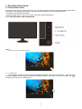
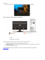
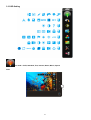
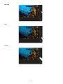
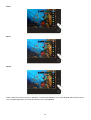
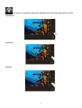
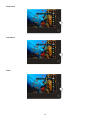
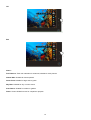
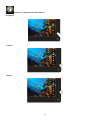
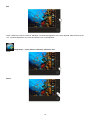
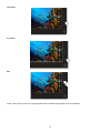
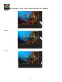
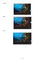
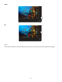
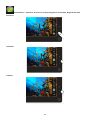
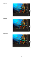
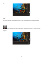
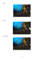
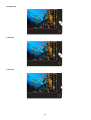
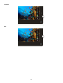
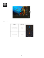
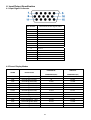
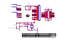
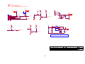
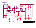
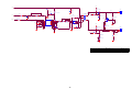
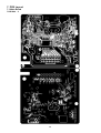
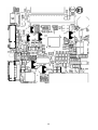
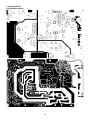
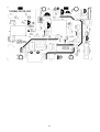
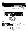
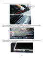
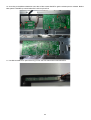
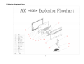
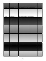
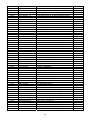
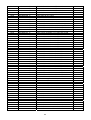
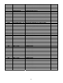
18.5" LCD Monitor
AOC N936Sw
Service
Service
Service
Horizontal Frequency
30-81 kHz
TABLE OF CONTENTS
Description
Page
Description
Page
Table of Contents…………………..…………………..…...1
6.1.Main Board..…….…...........................................32
Revision List.…...................................................……......2
6.2.Power Board..……….........................................36
Important Safety Notice.….….............................……......3
7.PCB Layout..………..............................................38
1.Monitor Specification..............................………............4
7.1.Main Board………..…........................................38
2.LCD Monitor Description……….…………………….......5
3.Operation Instruction.…………...................……...........6
7.2.Power Board….…..............................................40
3.1.General Instructions....................................…..........6
7.3.Key Board………..…..........................................42
3.2.Control Buttons and Connections...............................6
7.4.USB Board………..….........................................42
3.3.OSD Setting…...........................................................8
8.Maintainability………............................................43
4.Input/Output Specification...............……………….......27
8.1.Equipments and Tools Requirement…...............43
4.1.Input Signal Connector...............………..................27
8.2.Trouble Shooting…..………...............................44
4.2.Preset Display Modes……..........................27
9.White-Balance,Luminance Adjustment…............48
4.3.Panel Specification…………..………………………..28
5.Block Diagram….........................................................30
10.Mechanical Instructions …............ ..............50
5.1.Main Board…..….............................................30
11.Monitor Exploded View……................................64
5.2.Power Board…………..…………………………......31
12.BOM List…………..……………………….............71
6.Schematic…………..….........................................32
SAFETY NOTICE
ANY PERSON ATTEMPTING TO SERVICE THIS CHASSIS MUST FAMILIARIZE HIMSELF WITH THE
CHASSIS AND BE AWARE OF THE NECESSARY SAFETY PRECAUTIONS TO BE USED WHEN SERVICING
ELECTRONIC EQUIPMENT CONTAINING HIGH VOLTAGES.
CAUTION: USE A SEPARATE ISOLATION TRANSFOMER FOR THIS UNIT WHEN SERVICING
1
Revision List
Revision
Date
Revision History
Remark
T8AMM5NK6WA1NNE
T8AMM5NQ6WA1NNE
T8BAM5NQ6WA1NNE
A00
Aug.-01-2011
Initial release
T8BGM5NQ6WA1NNE
T8BAM5NQ6WA2NNE
T8BAM5NQ6WA1N6E
2
Important Safety Notice
Proper service and repair is important to the safe, reliable operation of all AOC Company Equipment. The service
procedures recommended by AOC and described in this service manual are effective methods of performing service
operations. Some of these service operations require the use of tools specially designed for the purpose. The
special tools should be used when and as recommended.
It is important to note that this manual contains various CAUTIONS and NOTICES which should be carefully read in
order to minimize the risk of personal injury to service personnel. The possibility exists that improper service
methods may damage the equipment. It is also important to understand that these CAUTIONS and NOTICES ARE
NOT EXHAUSTIVE. AOC could not possibly know, evaluate and advise the service trade of all conceivable ways in
which service might be done or of the possible hazardous consequences of each way. Consequently, AOC has not
undertaken any such broad evaluation. Accordingly, a servicer who uses a service procedure or tool which is not
recommended by AOC must first satisfy himself thoroughly that neither his safety nor the safe operation of the
equipment will be jeopardized by the service method selected.
Hereafter throughout this manual, AOC Company will be referred to as AOC.
WARNING
Use of substitute replacement parts, which do not have the same, specified safety characteristics may create shock,
fire, or other hazards.
Under no circumstances should the original design be modified or altered without written permission from AOC.
AOC assumes no liability, express or implied, arising out of any unauthorized modification of design.
Servicer assumes all liability.
FOR PRODUCTS CONTAINING LASER:
DANGER-Invisible laser radiation when open AVOID DIRECT EXPOSURE TO BEAM.
CAUTION-Use of controls or adjustments or performance of procedures other than those specified herein may
result in hazardous radiation exposure.
CAUTION -The use of optical instruments with this product will increase eye hazard.
TO ENSURE THE CONTINUED RELIABILITY OF THIS PRODUCT, USE ONLY ORIGINAL MANUFACTURER'S
REPLACEMENT PARTS, WHICH ARE LISTED WITH THEIR PART NUMBERS IN THE PARTS LIST SECTION OF
THIS SERVICE MANUAL.
Take care during handling the LCD module with backlight unit
-Must mount the module using mounting holes arranged in four corners.
-Do not press on the panel, edge of the frame strongly or electric shock as this will result in damage to the screen.
-Do not scratch or press on the panel with any sharp objects, such as pencil or pen as this may result in damage to
the panel.
-Protect the module from the ESD as it may damage the electronic circuit (C-MOS).
-Make certain that treatment person’s body is grounded through wristband.
-Do not leave the module in high temperature and in areas of high humidity for a long time.
-Avoid contact with water as it may a short circuit within the module.
-If the surface of panel becomes dirty, please wipe it off with a soft material. (Cleaning with a dirty or rough cloth may
damage the panel.)
3
1. Monitor Specifications
LCD Panel
Resolution
Model number
N936Sw
Driving system
TFT Color LCD
Viewable Image Size
47.0cm diagonal
Pixel pitch
0.3mm(H) x 0.3mm(V)
Video
R, G, B Analog lnterface & Digital Interface
Separate Sync.
H/V TTL
Display Color
16.7M Colors
Dot Clock
85.5MHz
Horizontal scan range
30 kHz - 81 kHz
Horizontal scan Size(Maximum)
409.8mm
Vertical scan range
55 Hz - 75 Hz
Vertical scan Size(Maximum)
230.4mm
Optimal preset resolution
1366x768 (60 Hz)
Highest preset resolution
1366x768 (60 Hz) )
Plug & Play
VESA DDC2B/CI
Input Connector
D-Sub 15pin
Input Video Signal
Analog: 0.7Vp-p(standard), 75 OHM
Power Source
100-240V~, 50/60Hz
Power Consumption
Physical
Characteristics
Standby < 1 W
Connector Type
15-pin Mini D-Sub
Signal Cable Type
Detachable
Dimensions & Weight:
Temperature:
Environmental
Typical < 25W
Humidity:
Altitude:
Height (with base)
358.66mm
Width
463.14mm
Depth
186mm
Weight (monitor only)
Weight (with
packaging)
Operating
3.13 kg
Non-Operating
-20°to 60°
Operating
10% to 85% (non-condensing)
Non-Operating
5% to 80% (non-condensing)
Operating
0~ 3000m (0~ 10000 ft )
Non-Operating
0~ 5000m (0~ 15000 ft )
4
4.18kg
0° to 40°
2. LCD Monitor Description
The LCD MONITOR will contain a main board, a power board, a key board and two USB boards which house the flat
panel control logic, brightness control logic and DDC.
The power board will provide AC to DC Inverter voltage to drive the backlight of panel and the main board chips
each voltage.
Monitor Block Diagram
CCFL Drive.
Flat Panel and
CCFL backlight
Power board
(Include: adapter, inverter)
RS232 Connector
For white balance
adjustment in factory
mode
Main Board
Key board
USB board*2
AC-IN
100V-240V
Video signal DDC
HOST Computer
5
3. Operating Instructions
3.1 General Instructions
Press the power button to turn the monitor on or off. The other control knobs are located at front panel of the monitor
(See Figure ). By changing these settings, the picture can be adjusted to your personal preferences.
* The power cord should be connected.
* Press the power button to turn on the monitor. The power indicator will light up.
3.2 Control Buttons and Connections
Power
Press to turn on or turn off the monitor.
4 : 3 or wide / Up
Press key to change the screen aspect ratio between standard 4:3 format or Wide format. When the input
resolution is wide format, the aspect ratio hotkey is disabled. When the main menu or sub-menu is active, the key
functions as to select up or increase value.
6
Auto / Down
Auto configure hot key: When the OSD is closed, press Auto button to do auto configure.
Cable Connections On Back of Monitor and Computer
1. Power
2. Analog (DB-15 VGA cable)
To protect equipment, always turn off the PC and LCD monitor before connecting.
1. Connect the power cable to the AC port on the back of the monitor.
2. Connect one end of the 15-pin D-Sub cable to the back of the monitor and connect the other end to the
computer's D-Sub port.
3. Turn on your monitor and computer.
If your monitor displays an image, installation is complete. If it does not display an image, please refer
Troubleshooting.
7
3.3 OSD Setting
Eco mode ---DCR, Standard, Text, Internet, Game, Movie, Sports
DCR
8
Standard
Text
Internet
9
Game
Movie
Sports
Notes : When Eco mode is not set as “Standard”, Contrast and Brightness can not be adjusted; When DCR is set as
“On”, Contrast, Brightness, Eco mode and Gamma can not be adjusted.
10
Color Boost --- Full Enhance, Nature Skin, Sky-Blue, Green Field, Auto Detect, Demo, Off, Exit
Full Enhance
Nature Skin
Sky-Blue
11
Green Field
Auto Detect
Demo
12
Off
Exit
Notes :
Full Enhance: Total color saturation is enhanced, suitable for vivid pictures.
Natural Skin: Suitable for human portrait.
Green Field: Suitable for large area of green.
Sky Blue: Suitable for sky or ocean scene.
Auto Detect: Suitable for outdoor or garden.
Demo: Screen divided into two for comparison purpose.
13
Luminance ---Brightness,Contrast, Gamma
Brightness
Contrast
Gamma
14
Exit
Notes : When Eco mode is not set as “Standard”, Contrast and Brightness can not be adjusted; When DCR is set as
“On”, Contrast, Brightness, Eco mode and Gamma can not be adjusted.
Image Setup --- Clock, Phase, H.Position, V.Position, Exit
Clock
Phase
15
H.Position
V.Position
Exit
Notes : When the input source is digital signal like DVI or HDMI, Image Setup can not be adjusted.
16
Color Temperature ---User-R , User-G , User-B, Normal, Warm, Cool, sRGB, Exit
User-R
User-G
User-B
17
Normal
Warm
Cool
18
sRGB
Exit
Notes :
One of DCR, Color Boost, and Picture Boost functions is active, the other two function is turned off accordingly.
19
Picture Boost --- V.Position, H.Position, Contrast, Brightness, Frame Size, Bright Frame, Exit
V.Position
H.Position
Contrast
20
Brightness
Frame Size
Bright Frame
21
Exit
Notes :
One of DCR, Color Boost, and Picture Boost functions is active, the other two function is turned off accordingly.
Extra ---Language, Reset, DDC-CI,OSD Timeout, Transparency, V. Position, H. Position, Off Timer,
Exit
Language
22
Reset
DDC-CI
OSD Timeout
23
Transparency
V. Position
H. Position
24
Off Timer
Exit
25
Exit
LED Indicator
26
4. Input/Output Specification
4.1 Input Signal Connector
Pin Number
1
2
3
4
5
6
7
8
9
10
11
12
13
14
15
15-Pin Side of the Signal Cable
Video-Red
Video-Green
Video-Blue
N.C.
Detect Cable
GND-R
GND-G
GND-B
+5V
Ground
N.C.
DDC-Serial data
H-sync
V-sync
DDC-Serial clock
4.2 Preset Display Modes
STAND
HORIZONTAL
VERTICAL
FREQUENCY(kHz)
FREQUENCY(Hz)
RESOLUTION
VGA
640×480 @60Hz DMT
31.469
59.94
VGA
640×480 @67Hz MAC
35
66.667
VGA
640×480 @72Hz DMT
37.861
72.809
VGA
640×480 @75Hz DMT
37.5
75
Dos-mode
720×400 @70Hz DOS
31.469
70.087
SVGA
800×600 @56Hz DMT
35.156
56.25
SVGA
800×600 @60Hz DMT
37.879
60.317
SVGA
800×600 @72Hz DMT
48.077
72.188
SVGA
800×600 @75Hz DMT
46.875
75
SVGA
832×624 @75Hz
49.725
74.55
XGA
1024×768 @60Hz DMT
48.363
60.004
XGA
1024×768 @70Hz DMT
56.476
70.069
XGA
1024×768 @75Hz DMT
60.023
75.029
WXGA
1366x768 @60Hz DMT
47.765
59.85
27
4.3 Panel Specification
4.3.1 General Features
M185B1-L07 is a 18.5” TFT Liquid Crystal Display module with 2 CCFL Backlight unit and 30pin 1ch-LVDS interface.
This module supports 1366 x 768 WXGA mode and can display up to 16.7M colors. The inverter module for
Backlight is not built in.
4.3.2 General Specifications
4.3.3 Electrical Characteristics
1.TFT LCD Module
(Ta= 25±2℃, VCC=5.0V, Fv=60Hz)
2 .Back Light Unit
28
4.3.4 Optical Characteristics
29
5.Block Diagram
5.1 Main Board
TSUM1PFR
SCHEMATIC
XGA/SXGA
DSUB_5V
VCC3.3
CMVCC1
LVDS OUTPUT
DSUB_R+
DSUB_RDSUB_G+
DSUB_GDSUB_SOG
DSUB_B+
DSUB_BDSUB_H
DSUB_V
DSUB_5V DDC1_SDA
DDC1_SCL
DET_CABLE
DSUB_R+
DSUB_RDSUB_G+
DSUB_GDSUB_SOG
DSUB_B+
DSUB_BDSUB_H
DSUB_V
DDC1_SDA
DDC1_SCL
DET_CABLE
VCC3.3
EDID_CTRL
EDID_CTRL
VCC1.8
VCC3.3
VCC1.8
CMVCC
VCC3.3
CMVCC1
CMVCC
CMVCC1
CMVCC1
02.Input
VCC1.8
CMVCC
VCC3.3
DSUB_5V
CMVCC
CMVCC1
PA[0..1]
PA[0..1]
VCC1.8
on_BACKLIGHT
on_BACKLIGHT
VCC3.3
PA[4..9]
PA[4..9]
PB[0..9]
PB[0..9]
Mute
Volume#
DSUB_5V PANEL_ID#
Mute
Volume#
PANEL_ID#
Adj_BACKLIGHT
CMVCC
VCTRL
Adj_BACKLIGHT
PPWR_ON#
PA[0..1]
CMVCC
PA[4..9]
PB[0..9]
PPWR_ON#
VCTRL
CMVCC1
05.Power
03.Scalar
04.Output
OEM MODEL OTS R-series
Size
絬隔瓜絪腹
G3324-I-X-X-6-090105
TPV MODEL
Rev
Key Component
01.Top
PCB NAME
TPV
Date
( Top
Victory
Electronics
Co . ,
Tuesday , January 06, 2009
Ltd. )
Sheet
30
715G3244-I
3
of
7
称爹
A
F
<称爹>
5.2 Power Board
AC input
Bridge
Rectifier
and Filter
EMI filter
Transformer
(T901)
14.5V
Rectifier
diodes
5V
Start Resistor
(R908)
Power Switch
(Q901)
PWM Control
LD7576
(U901)
Photo coupler
(U902)
Output
Circuit
Transformer
(T801)
MOSFET
(Q803)
Feedback
Circuit
Regulator
(U903)
14.5V
Lamp
PWM Control
AM9000ES
(U801)
Feedback
Circuit
31
DIM
ON/OFF
6. Schematic
6.1 Main Board
715G3244
2
H_Sy nc
V_Sy nc
VCC3.3
VCC3.3
R120
R101 0R05 1/10W 5%
R105
2K2 1/16W 5%
7
R102 100R 1/16W 5%
R103 100R 1/16W 5%
DSUB_H
DSUB_V
5
5
VGA_B+
R106
C102 C103
2K2 1/16W 5%
22pF 22pF
FB102
R104
1
C101
2
BEAD
100R 1/16W 5%
C104
R107
75R 1/16W 5%
R121
5pF/50V
R108
DDC1_SCL
DDC1_SCL
16
R110
NC/100R 1/16W 5%
DSUB_SCL
DB15
10
5
9
4
8
3
7
2
6
1
15
14
DDC1_SDA
DDC1_SDA
13
12
11
100R 1/16W 5%
VGA_BVGA_B+
VGA_GVGA_G+
VGA_RVGA_R+
DSUB_5V
ZD103
RLZ5.6B
R109
5
FB103
1
VGA_G+
R111
U103
AZC199-04S
I/O1 I/O4
GNDVDD
I/O2 I/O3
5pF/50V
R114
H_Sy nc
VGA_R+
1
10K 1/16W 5%
NC
R110
100R 1/16W 5%
NC
R113
100R 1/16W 5%
NC
NC
U405
NC
M24C02-WMN6TP
Q407
NC
2N3904S-RTK/PS
R472
NC
4K7 1/16W 5%
R473
NC
4K7 1/16W 5%
R474
NC
4K7 1/16W 5%
R475
NC
47R 1/16W 5%
R476
NC
47R 1/16W 5%
C434
NC
0.22uF
75R 1/16W 5%
VGA_G+
VGA_R+
1
2
3
5
DSUB_R-
5
0.047uF
5pF/50V
R117
C113
100R 1/16W 5%
0.047uF
U102
AZC199-04S
I/O1 I/O4
GNDVDD
I/O2 I/O3
DSUB_5V
CMVCC1
6
5
4
VGA_B+
D403
BAV70
CMVCC1
BAV70
3
D403
100R 1/16W 5%
C111
1
R121
DSUB_R+
C110
VGA_R-
2
NC
R115
2
R116
DSUB_SCL R475
DSUB_SDA R476
47R 1/16W 5%
47R 1/16W 5%
R474
4K7 1/16W 5%
10K 1/16W 5%
5
0.047uF
BEAD
V_Sy nc
EDID external
R120
DSUB_G-
C109
FB101
6
5
4
R473
4K7 1/16W 5%
EDID internal
5
0.047uF
100R 1/16W 5%
DSUB_SCL
DSUB_G+
C107
100R 1/16W 5%
C108
R112
1
2
3
5
0.047uF
2
75R 1/16W 5%
DSUB_SDA
DSUB_SOG
C106
390 OHM 1/16W
ZD104
RLZ5.6B
VGA_G-
DGND
5
DSUB_5V
BEAD
GND POWER
DSUB_B0.047uF
VGA_PLUG
DSUB_5V
17
5
R113
NC/100R 1/16W 5%
DSUB_SDA
CN101
R472
4K7 1/16W 5%
5
NC/10K 1/16W 5%
5
C105
VGA_BNC/10K 1/16W 5%
DSUB_B+
0.047uF
CMVCC1
5
C434
U405
8
7
6
5
0.22uF16V
VCC A0
WP
A1
SCL A2
SDA VSS
1
2
3
4
R118
10K 1/16W 5%
VGA_PLUG
M24C02-WMN6TP
DET_CABLE
5
R122
DDC1_SDA
DDC1_SCL
NC
Q407
LMBT3904LT1G
4K7 1/16W 5%
EDID_CTRL
OEM MODEL AOC 836S
Size
絬隔瓜絪腹
G3244-G-X-X-6-090105
TPV MODEL
Rev
Key Component
02.Input
PCB NAME
T P V ( Top
Date
32
R123
Victory
Electronics
Co . ,
Tuesday , January 06, 2009
Ltd. )
Sheet
715G3244-I
4
of
7
称爹
B
F
<称爹>
AVDD VCC3.3
VCC1.8
SST
3
3
3
3
3
3
3
3
3
3
3
U402
010A
Befor AOC ID2007 OSD
020A
For ID2008 ID2009
Eon
6
30
53
VCTRL
LVA3P
LVA3M
LVA2P
LVA2M
LVA1P
LVA1M
LVA0P
LVA0M
52
VCTRL
33
34
PA0
PA1
35
36
37
38
39
40
PA4
PA5
PA6
PA7
PA8
PA9
PA[0..1]
4
R403 390 OHM 1/16W
15
C401
14
0.1uF/16V
C408
0.22uF16V
LVB3P
LVB3M
LVBCKP
LVBCKM
LVB2P
LVB2M
LVB1P
LVB1M
LVB0P
LVB0M
REXT
1
2
WP 3
4
8
7
6
5
CS# VCC
DO HOLD#
WP# CLK
VSS
DI
EN25F20-100GCP
CMVCC1
21
22
23
24
R456
R457
0R05 1/16W
0R05 1/16W
R405
100R 1/16W 5%
28
+
54
C412 47pF
1
LVDS
SDO
SCZ
SCK
SDI
GPIO_P15/PWM0
PWM2/GPIO_P24
GPIO_P12
PWM1/GPIO_P25
RSTN
GPIO_P00/SAR1
GPIO_P01/SAR2
GPIO_P27/PWM1
20
27
0R05 1/16W
R402
2
C407
5
0.1uF/16V
For RSTN detect
function
R424
57
58
59
R425
C418
NC
NC
7
CMVCC
R458
NC/10K 1/16W 5%
NC
R411
R412
100R 1/16W 5%
100R 1/16W 5%
R414
R410
R418
10K 1/16W 5%
1K 1/16W 5%
NC/100R 1/16W 5%
R419
NC/100R 1/16W 5%
on_BACKLIGHT
adj_BACKLIGHT
7
7
Volume#
7
Mute
7
R485
0R05 1/16W
R426
NC/100R 1/16W 5%
Q401
NC/AO3401
EDID_CTRL
PANEL_ID#
R452
NC
R420
NC/100R 1/16W 5%
POWER_KEY #
R451
NC
R459
NC/47K 1/16W 5%
7
R406
MSDA
NC/6K8 1/16W 5%
KEY 2
KEY 1
C409
RST
GPIO_P06
GPIO_P07
PWM0/GPIO_P26
GPIO_P13
GPIO_P14
XIN
60
61
62
63
64
LED_G/B
LED_O
R409
NC/0.1uF/16V
Max condition for LED:
1. Vcc = 3.3 V
2. Current = 12 mA
FW need to be modified.
XOUT
CMVCC1
CMVCC
EE_WP
NC/10K 1/16W 5%
MSCL
VCC3.3
C429
+
C430
NC/10uF/50V
GPIO_P10/I2C_MCL
GPIO_P11/I2C_MDA
R460
31
32
3
5
29
NC
MODE[0]
MODE[1]
26
25
R413
PPWR_ON#
DET_CABLE
100R 1/16W 5%
NC
R478
R427
U403
VCC NC
WC
E1
SCL E2
SDA VSS
NC
1
2
3
4
0R05 1/10W 5%
C415
C416
NC/0.1uF/16V0.1uF/16V
R404
NC/0R05 1/16W
NC/0R05 1/16W
C417
NC/10K 1/16W 5% NC/0.1uF/16V
Near to Connect
VCC3.3
1
2
3
4
5
6
R407
10K 1/16W 5%
LED_GRN/BLUE
200 OHM 1/16W
CN407
NC/150 OHM
FB405
TOUCH POWER
1
2
3
4
5
6
7
U403
C419
Without NVRAM
M24C04-WMN6TP
When NVRAM is used,
POWER_KEY# and PANEL_ID#
will not be used at same
time.
NC
NC
0.22uF16V
R424
100R 1/16W 5%
NC
R451
100R 1/16W 5%
NC
R452
100R 1/16W 5%
NC
R453
10K 1/16W 5%
NC
NC
R425, C418 depend on
case.
VCC3.3
R482
R469
1K 1/16W 5%
NC/CONN
FB404
LED_ORANGE/TOUCH VCC
R468
CMVCC1
CN402
R461
R462
For NVRAM
Q403
LMBT3906LT1G
R481
NC/0R05 1/16W
LED_O
1
ZD403
NC/UDZSNP5.6B
1
LED_G/B
NC/CONN
2
2
C414
NC/0.1uF/16V
ZD402
NC/UDZSNP5.6B
1
2
NC
3.9K OHM 1/16W
KEY 1
KEY 2
POWER_KEY #
LED_GRN/BLUE
LED_ORANGE/TOUCH VCC
C413
NC/0.1uF/16V
1
2
3
4
5
6
7
8
R428
NC/10K 1/16W 5%
3.9K OHM 1/16W
1
NC
NC
2
R463
R464
R484
0R05 1/16W
TOUCH POWER
8
7
6
5
EE_WP
R467
3
R483
CN409
NC
NC/M24C04-WMN6TP
R466
2K2 1/16W 5%
LED_ORANGE/TOUCH VCC
ZD404
NC/UDZSNP5.6B
R455
NC
CMVCC1
VCC3.3
6
5
4
3
2
1
R454
NC
TSUM1PFR-LF
CN406
CN408
R453
MSCL
MSDA
According to MST's
request, reserve another
RST circuit.
R421
6
4
GND
GND
GND
7 CMVCC
7
6
5
4
3
2
1
PB[0..9]
PB0
PB1
PB2
PB3
PB4
PB5
PB6
PB7
PB8
PB9
55
56
CMVCC
NC/CONN
VCC1.8
REFM
X401
14.31818MHz
1
C411 47pF
10K 1/16W 5%
R401
0R05 1/16W
2
R417
41
42
43
44
45
46
47
48
49
50
REFP
U402
C410
10uF/50V
5
0.1uF/16V
VCC1.8
PB[0..9]
VCC3.3
CMVCC1
PA[4..9]
C404
0.1uF/16V
0.1uF/16V
AVDD
R408
5
300OHM
C403
C406
For All model
10K 1/16W 5%
PA[0..1]
AVDD
FB401
VCC3.3
7
7
PA[4..9]
U402
020
7
RIN0P
RIN0M
GIN0P
GIN0M
SOGIN0
BIN0P
BIN0M
HSY NC0
VSY NC0
DDCA_SDA/RS232_TX
DDCA_SCL/rs232_RX
7
VDDC
VDDC
13
12
10
9
11
8
7
16
17
18
19
DSUB_R+
DSUB_RDSUB_G+
DSUB_GDSUB_SOG
DSUB_B+
DSUB_BDSUB_H
DSUB_V
DDC1_SDA
DDC1_SCL
VDDP
For user data, WB, EDID,
HDCP are saved in
Flash.
Eon
AVDD_ADC
SST
U401
51
VCC3.3
U402
0R05 1/16W
R470
0R05 1/10W 5%
PANEL_ID# and POWER_KEY#
could be optional.
R454
10K 1/16W 5%
Q402
LMBT3906LT1G
R455
10K 1/16W 5%
NC
R471
R426
NC
NC or 100R 1/16W 5%
R420
NC
NC or 100R 1/16W 5%
LED_ORANGE/TOUCH VCC
0R 1/16W 5%
When use touch
Key,GPIO_P07 as
to control touch
key VCC
150 OHM
CONN
ZD401
NC/RLZ5.6B
C433
NC/CONN
T P V ( Top
1uF 10V
Electronics
Co . ,
Ltd. )
OEM MODEL AOC 836S
Size
G3244-G-X-X-6-090105
TPV MODEL
Rev
03.Scalar
PCB NAME
Date
33
Victory
絬隔瓜絪腹
Key Component
Sunday , May 31, 2009
Sheet
715G3244-I
5
of
7
称爹
C
F
<称爹>
PANEL_VCC
5
PA[0..1]
PA[0..1]
CN403
PA0
PA1
5
PA[4..9]
PA[4..9]
R477
R434
NC/150R 1/4W 5%
330 OHM 1/4W
PA4
PA5
PA6
PA7
PA8
PA9
5
PB[0..9]
1
2
3
4
5
6
7
8
9
10
11
12
13
14
15
16
17
18
19
20
21
22
23
24
25
26
27
28
29
30
C420
0.1uF/16V
PA0
PA1
PB2
PB3
PA4
PA5
PB[0..9]
PA6
PA7
PB0
PB1
PB2
PB3
PB4
PB5
PB6
PB7
PB8
PB9
PA8
PA9
PB0
PB1
PB2
PB3
3D
1
G
2
S
PB4
PB5
PB6
PB7
PB8
PB9
AO3401L
CMVCC
CMVCC
2
4
6
8
10
12
14
16
18
20
22
24
26
28
30
PA0
PB2
PA4
PA6
PA8
PB0
PB2
PB4
PB6
PB8
CONN
7
4
3
2
1
Q405
AO3401
Q411
NC/AO4411
D
D
D
D
R436
100K 1/16W 5%
PANEL_VCC
Q404
PMBS3906
5
6
7
8
PPWR_ON#
G
S
S
S
10K 1/16W 5%
4K7 1/16W 5%
PPWR_ON#
PA1
PB3
PA5
PA7
PA9
PB1
PB3
PB5
PB7
PB9
1
3
5
7
9
11
13
15
17
19
21
23
25
27
29
C419
0.1uF/16V
R433
5
CN405
NC/CONN
2006-11-7 Add pull up 4K7 to MVCC
R435
PANEL_VCC
FB402
C421
120OHM
+
100uF/25V
T P V ( Top
Victory
Electronics
Co . ,
Ltd. )
OEM MODEL AOC 836S
Size
Rev
絬隔瓜絪腹
G3244-G-X-X-6-090105
TPV MODEL
Key Component
04.Output
PCB NAME
Date
Sheet
Sunday , May 31, 2009
34
715G3244-I
6
of
7
称爹
A
F
<称爹>
2008/01/14
BAT99 : If 0.05A,VF=1.0V
BAV70 : If 0.05A,VF=1.0V
It's need to use Low Dropout Regulator.
DSUB_5V
CMVCC
CMVCC1
VCC3.3
VCC3.3
VCC3.3
1
2
DSUB_5V 2
5, 6 CMVCC
D401
NC/BAV99
CN404
3
NC/0 OHM 1/3W
9
8
7
6
5
4
3
2
1
D402
CMVCC
CMVCC
BKLT-VBRI
BKLT-EN
C_PANEL_INDEX
Volume
Mute
R450
PANEL_ID#
CMVCC1
5
R439
NC
10K 1/16W 5%
10K 1/16W 5%
VCC1.8
R440
Q406
LMBT3904LT1G
NC
NC
on_BACKLIGHT
5
C432
Q409
KN2907AS
4K7 1/16W 5%
Mute
VCC1.8
R479
NC/0R05 1/4W 5%
Q410
KN2907AS
C425
R449
5
R437
BKLT-EN
CMVCC1
NC
NC(R0402)
R480
2.2 OHM 2W
R465
5
5
+ C423
0.1uF/16V
100uF/25V
VCTRL
5
CONN
VCC3.3
VCC3.3
R441
1K 1/16W 5%
BKLT-VBRI
VCC3.3
CMVCC1
R446
R447
NC
NC/10K 1/16W 5%
MVCC
FB403
VCC3.3
VIN
VOUT
ADJ(GND)
Volume
R442
adj_BACKLIGHT
+ C426
5
C428
100uF/25V
100R 1/16W 5%
Q408
NC/LMBT3904LT1G
R448
NC/4K7 1/16W 5%
NC
Volume#
0.1uF/16V
5
3
2
1
VCC3.3
U404
AP1117D33L-13
C422
4, 5
+ C427
0.1uF/16V
100uF/25V
U404 can use package 223 or 252.
OEM MODEL AOC 836S
Size
絬隔瓜絪腹
G3244-G-X-X-6-090105
TPV MODEL
Rev
Key Component
05.Power
PCB NAME
T P V ( Top
Date
35
Victory
Electronics
Sunday , May 31, 2009
Co . ,
Ltd. )
Sheet
715G3244-I
7
of
7
称爹
B
F
<称爹>
6.2 Power Board
715G2892P01019001C
!
1
R929 100 OHM 1/4W
C916
R930 100 OHM 1/4W 0.001uF
F801
0R05 1/4W 5% +14.5V
2
+
BD901
KBP208G
2
3
R903 100 OHM 1/4W
2008-11-22
ZD901
MTZJ T-72 16B
R904
220 OHM 2W
C918
1000uF 25V
1
+
R905
470R 1/10W 5%
4
-
D901
NC/SR5150
1
2
C937
0.01uF/2KV
C938
!
+
!
C913
22uF/50V
R910 100 OHM 1/4W
8
7
6
5
C912
0.1uF/25V
R923
220 OHM 1/4W
!
C922
470uF 16V
+
D906
3
R914
43.2K OHM 1% 1/4W
C924
0.1uF/16V
R916
3.65K OHM 1% 1/10W
R928
1K 1/10W 1%
C902
1000PF/250VAC
C903
1000PF/250VAC
C900
0.0022UF
C915
U903
KIA431A-AT/P
2008-12-01
3
2
R925
2.43K OHM 1% 1/10W
R935
NC
!
!
+5V
R920
1K 1/10W 1%
R924
0.39 OHM 2W +-5%
F902
FUSE
FUSE
R919
150R 1/8W 5%
U902
PC123X2Y FZOF
2
C914
470pF
NR901
NTCR
F901
1000uF/16V
C925
+ C920
1000uF 25V
FMW-2156
!Q901
FB901
BEAD
C908
0.47uF/275V
+
D905 NC/31DQ06FC3
FMA07N65GX
R918
10K 1/10W 1%
L906
1
LD7576
0.047uF
C917
0.001uF
10
9
1
R917
10R 1/4W 5%
R907
1K 1/10W 1%
C923
0.001uF
R912 100 OHM 1/4W
D907
IN4148
R921
NC/100K 1/10W 1% U901
1
HV
2 CT
3 COMPNC
4 CS VCC
GNDOUT
620K OHM 1/4W
R934
NC
4
2
R913
1.5 OHM 1/4W +-5%
Q904
KTD1028
2
R909 100 OHM 1/4W
7
8
1
R902
C927
620K OHM 1/4W
12
11
5
2
D908
NC/IN4148
R901
620K OHM 1/4W
!
D902
SB5150
2
R933
NC
30mH
T901
POWER X'FMR
6
D904
FR103
!
1000PF/250VAC
!
1
D903
FR107
R908
10K OHM 1/4W +-5%
R932
NC
3 L901 4
2
C911
1500PF2KV
4
C909
NC/0.22uF/275V
!
100UF450V
NC
1
3
R931
!
R906
100KOHM +-5% 2WS
1
!
R900
C907
+
2008-12-01
1
CN902
2008-12-01
MUTE
CN901
SOCKET
HS1
HEAT SINK(Q901)
1
2
HS2
NC/HEAT SINK(D906_5V/4A)
VOL
+5V
1
2
ON/OFF
C926
0.1uF/16V
DIM
L907
NC
9
8
7
6
5
4
3
2
1
F903
+5V1
2008-12-01
NC
+
C921
NC
+
C931
NC
2008-12-01
Wire Harness
HS3
HEAT SINK(D906_5V/2.5A)
1
2
GND1
GND
1
2
936SW/2036S
Size
絬隔瓜絪腹
G2892-1-3-X-1-090204
TPV MODEL PWPC9921MHD1
Rev
Key Component
01.POWER
PCB NAME
TPV
Date
36
( Top
Victory
Electronics
Co . ,
Wednesday , February 04, 2009
Ltd. )
OEM MODEL
Sheet
715G2892-F-3
2
of
3
称爹
Custom
1
ODM MODEL
REF
+14.5V
+
C811
470uF 25V
R805
10K 1/10W 5%
0.1uF50V
R816
R803
RJ805
R811
10K 1/10W 5%
6
C815
C809
0.001uF
20K 1/10W 1%
8
7
6
5
4
3
2
1
R810
R809
100K 1/10W 5%
DBRT
EN
FSET
FT
COMP
LI2
LI1
OV2
VIN
BT
TG
SW
VCC
BG
GND
OV1
9
10
11
12
13
14
15
16
C806
0.047uF
RJ807
R813
Q803
RJ803
4
3
2
1
0R05 1/4W 5%
3.3 OHM +-5% 1/10W
0R05 1/4W 5%
G2
S2
G1
S1
D2
D2
D1
D1
R801
412 OHM 1/10W
D803
2
1
3
BAW56
8
1
5
6
7
8
RJ801
0R05 1/4W 5%
P8008HV
C808
REF
1uF 16V
C807
C802
0.0033uF/50V
3
4
2N2 50V
MPS10091
C810
10K 1/10W 5%
OV2
10K 1/10W 5%
C813
10 OHM +-5% 1/10W
0.01uF
ON/OFF
T801
7
POWER X'FMR
CONN
2K 1/10W 5%
R807
R815
0R05 1/4W 5%
R817
1
2
C801
LI1
10pF3KV
10 OHM +-5% 1/10W
DIM
CN801
C814
1uF 25V
C805
U801
0.0039uF/16V
LI2
1uF 16V
LI1
OV2
R812
OV1
R814
REF
10 OHM +-5% 1/10W
RJ806
0R05 1/4W 5%
C812
R806
10K 1/10W 5%
2N2 50V
CN802
R804
3.3 OHM +-5% 1/10W
1
2
C803
LI2
10pF3KV
CONN
RJ802
2K 1/10W 5%
R808
OV1
0R05 1/4W 5%
10K 1/10W 5%
C804
0.0033uF/50V
R802
412OHM 1/10W
RJ804
0R05 1/4W 5%
T P V ( Top
Electronics
Co . ,
Ltd. )
OEM MODEL
G2892-1-3-X-1-090204
TPV MODEL
Key Component
02.INVERTER
PCB NAME
Date
37
Victory
絬隔瓜絪腹
Wednesday , February 04, 2009
Sheet
936SW/2036S
Size
PWPC9921MHD1
Rev
715G2892-F-3
3
of
3
称爹
Custom
1
ODM MODEL
7. PCB Layout
7.1 Main Board
715G3244
2
38
39
7.2 Power Board
715G2892P01019001C
40
41
7.3 Key Board
715G3371
2
7.4 USB Board
715G3501
3
715G2663
3
42
8. Maintainability
8.1 Equipments and Tools Requirement
1.
Voltmeter.
2.
Oscilloscope.
3.
Pattern Generator.
4.
DDC Tool with an IBM Compatible Computer.
5.
Alignment Tool.
6.
LCD Color Analyzer.
7.
Service Manual.
8.
User Manual.
43
8.2 Trouble Shooting
1.No Power
No power
NG
Check power cable is
tightened?
Re-plug the power cable
OK
NG
Check Power “On/Off”
is “On”?
Turn on the Power “On/Off” switch
OK
NG
Check the LED
indicate is OK?
Check the AC power
OK
Replace the converter board
NG
Replace main board and check connections
NG
Replace key board and check connections
44
2. No Video (Power LED Blue)
No Video (Power LED Blue)
Press the power
button is OK?
NG
Replace the main board
OK
Replace the converter
board
OK
The end
NG
Replace the main
board and connection
OK
The end
NG
Check the LVDS/FFC
cable or panel
NG
Replace the key board
45
OK
Replace the LVDS/FFC
cable or panel
3.
DIM
DIM (image overlap, focus or flicker)
OK
Reset in factory mode
The end
NG
Set to the optimal
frequency, select the
recommended frequency
OK
The end
NG
Readjust the phase and pixel
clock in the user mode
OK
The end
NG
Pull out signal cable and
check “Self Test Feature
Check” is ok?
OK
Check the signal cable
and the PC
NG
NG
OK
Replace the main board
NG
Replace the panel
OK
46
The end
4. Color is not optimal
Color is not optimal
Color shift
Miss color
Reset the factory mode
Replace the signal cable
NG
OK
NG
In the user mode, set the” color
settings” until customer satisfy
The end
Pull out the signal cable
and check the screen
color display is normal?
NG
OK
NG
Replace the signal cable or PC
Replace the main board
47
9. White- Balance, Luminance Adjustment
Approximately 30 minutes should be allowed for warm up before proceeding white balance adjustment.
How to setting MEM channel you can reference to chroma 7120 user guide or simple use “SC” key and
“NEXT” Key to modify xyY value and use “ID” key to modify the TEXT description Following is the procedure to do
white-balance adjust .
1. Setting the color temp.
A. 6500K color
Warm color temp. parameter is
x=313±30 ,y=329±30
B. 7300K color
Normal color temp. parameter is x=301±30 ,y=317±30
C. 9300K color
Cool color temp. parameter is
x=283±30,y=297±30
D. sRGB color:
sRGB color temp. parameter is x=313±30 ,y=329±30
2. Enter into the factory mode:
Turn off the power, then press ∧ key,∨ key and press the Power button at the same time, the next, press the
Menu button, the factory OSD will be at the left top of the panel.
3. Bias adjustment:
Set the Contrast
to 50; Adjust the Brightness
to 90.
4. Gain adjustment:
A. Adjust Warm (6500K) color-temperature
1. Switch the chroma-7120 to RGB-Mode (with press “MODE” button)
2. Switch the MEM.channel to Channel 3 (with up or down arrow on chroma 7120)
3. The LCD-indicator on chroma 7120 will show x=313±30 ,y=329±30
4. Adjust the RED on factory window until chroma 7120 indicator reached the value R=100
5. Adjust the GREEN on factory window until chroma 7120 indicator reachedthe value G=100
6. Adjust the BLUE on factory window until chroma 7120 indicator reached the value B=100
7. Repeat above procedure (item4, 5, 6) until chroma 7120 RGB value meet the tolerance =100±2
B. Adjust Normal (7300K) color-temperature
1. Switch the chroma-7120 to RGB-Mode (with press “MODE” button)
2. Switch the MEM.channel to Channel 4(with up or down arrow on chroma 7120)
3. The LCD-indicator on chroma 7120 will show x=301±30 ,y=317±30
4. Adjust the RED on factory window until chroma 7120 indicator reached the value R=100
5. Adjust the GREEN on factory window until chroma 7120 indicator reachedthe value G=100
6. Adjust the BLUE on factory window until chroma 7120 indicator reached the value B=100
7. Repeat above procedure (item 4, 5, 6) until chroma 7120 RGB value meet the tolerance =100±2
48
C. Adjust Cool (9300K) color-temperature
1. Switch the Chroma-7120 to RGB-Mode (with press “MODE” button)
2. Switch the MEM. Channel to Channel 9 (with up or down arrow on chroma 7120)
3. The LCD-indicator on chroma 7120 will show
x=283±30,y=297±30
4. Adjust the RED on factory window until chroma 7120 indicator reached the value R=100
5. Adjust the GREEN on factory window until chroma 7120 indicator reached the value G=100
6. Adjust the BLUE on factory window until chroma 7120 indicator reached the value B=100
7. Repeat above procedure (item 4, 5, 6) until chroma 7120 RGB value meet the tolerance =100±2
D. Adjust sRGB color-temperature
1. Switch the chroma-7120 to RGB-Mode (with press “MODE” button)
2. Switch the MEM.channel to Channel 10 (with up or down arrow on chroma 7120)
3. The LCD-indicator on chroma 7120 will show x=313±30 ,y=329±30
4. Adjust the RED on factory window until chroma 7120 indicator reached the value R=100
5. Adjust the GREEN on factory window until chroma 7120 indicator reachedthe value G=100
6. Adjust the BLUE on factory window until chroma 7120 indicator reached the value B=100
7. Repeat above procedure (item 4, 5, 6) until chroma 7120 RGB value meet the tolerance =100±2
E. Turn the Power-button off to quit from factory mode.
49
10.Mechanical Instructions
1.Put the monitor on the EPE pad.
2.Lay down the monitor, then use cross screwdriver or the expert tools leave off the stand while press the Push area
of the back cover.
3.Overturn the monitor and the top towards to us.
50
4.Take apart the front frame with hands on the label area.
5.As the center of one side of USB connector, take apart 3 sides and stop. Attention: Do not break off the key pc
side, or pull the front frame forcibly, to avoid the keypad peel off.
6.Overturn the monitor, on the USB connector area, one hand press the Panel, and use the other to undrawn the
back cover.
51
7.Make the notice that the front frame of the key pc side should be separated at last.
8. In turn to take apart the key pc connect PIN (A&B), lamp line (C&D), peel off the aluminum foil (E&F), draw off the
FFC pin (G), if there is defect with main pc, need leave of f the six-angle screw (H).
9.Withdraw the front frame from the Panel side. Use screwdriver to take off the screw which used to fix the iron
frame and Panel, and then take apart them.
52
10. According to the different defective area, take off the screws ABCDE to get the relevant part to maintain. Before
take apart the POWER pc should take off the AC iron piece first.
11. Use little screwdriver to peel off the key pc from the front frame when need maintain it.
53
11.Monitor Exploded View
*936*
54
12. BOM List
Note: The parts information listed below are for reference only, and are subject to change without notice. Please go
to http://cs.tpv.com.cn/hello1.asp for the latest information.
T8AMM5NK6WA1NNE
Location
E08905
E08905
E08902
E08902
E08902
E08901
E08901
E09503
E09503
E09503
E09501
E09501
E750
E09501
Part No.
052G 1186
052G 1208 A
052G 1211 B
052G 1211550
052G 2191 A
089G 175 8A C
089G 175 8A G
089G 715CAAE01
089G 715GAAE01
089G 715HAAE01
089G402A15N HL
089G402A15N IS
095G8014 7DW06
095G8014 7TW06
095G8014 7WW06
095G8018 3DH92
095G8018 3TH92
0D1G1030 8120
0M1G 130 5120
705GH934024
750GLM185B1732N000
H40G 001624 1A
H40G 18N61556A
H40G 45762413B
H40G 58161569A
H40G 58361576A
H40G 58461558B
H41G780061580B
H44G8018101
H44G8018201
H44G8018615 8A
H45G 87 18 23
H70G2011615 5A
KEPCBHA8
PWPCA921MHD2
Q15G0413G02
Q34G0558AEDB2B0100
Q34G0559AEDAKS0100
Q40G 58162435A
Q45G 76 28 H A
Q45G 76 28V13 A
Q50G 4 10
Q52G 1185 99
Q85G0118101
S95G80183H92
USB9HA1
USBAHA5
0Q1G1040 8120
Q01G6064 1
Description
SMALL TAPE
AL FOIL
Conductive Tape 85mm *40mm *0.09mm
ALUMINUM FOIL TAPE
PAPER TAPE
USB CABLE 1800MM without PE bag
USB CABLE 1800MM without PE bag
SIGNAL CABLE
SIGNAL CABLE
SIGNAL CABLE
AC POWER CORD 1500mm
AC POWER CORD 1500MM
HARNESS 7P(2008)-6P 450
HARNESS 7P(2008)--6P(11013) 450
HARNESS 7P(2008)-6P(1005) 450
LVDS CABLE 30P-30P 140MM
HARNESS 30P-30P(2004) 140
screw
SCREW
18.5"LCD STAND-BASE ASS'Y
LCD M185B1-L07 C2/C5(C6) NB CMI
CARTON LABEL BARCODE 1
N936Sw EPI ID LABEL
P/N LABEL FOR BASE
USB LABEL
WIN7
N936Sw FRENCH LABEL
QSG
EPS 936S
EPS 936S
N936Sw CARTON
EPE COVER
N936Sw CD MANUAL
KEY BOARD
POWER BOARD
MAIN FRAME
bezel L185WA-936
rearcover L185WA-936
LABEL
PE BAG FOR MANUAL
PE BAG
TIE (Y1900221)
TAPE
AOC 936S AC SHIELD
HARNESS 30P-30P 140MM
USB BOARD
USB BOARD
SCREW 4x8
NO-SUGGEST screw
55
Remark
2nd source
2nd source
2nd source
2nd source
2nd source
2nd source
2nd source
2nd source
SMTCA-U402
CN409
CN404
R480
CN101
X401
CN405
GND1
CN802
CN801
U902
NR901
C908
C937
C801
C803
C902
C903
C900
C925
C918
C920
C811
C922
C907
L901
L906
T901
T801
CN901
D902
CN902
CN902
BD901
CN511
CN512
CN501
CN502
Q34G0560AED 1S0100
Q34G0561AED 1S0100
Q34G0562AED 2S0130
Q37G0133011
756GHACB A1142
100GAMM8020W11
033G3802 7B Y L
033G3802 9B Y L
061G152M22964L SY
088G 35315F CH
093G 22 53 YC
311GW200C30ABL
709G3244 HM002
AIGAM5A1H2
H40G 45762429A
A33G0564 2 1L0100
H52G1201 1
SMTKEPCBHA8
009G6005 1
033G8021 2E L
033G8021 2E L
056G 139 3A
061G 5810X
063G107K2246S1
065G 2M103 3B
065G 3J5096ET
065G 3J5096ET
065G305M1022BP
065G305M1022BP
065G306M2222BP
067G215P1023AV
067G215P1024AV
067G215P1024AV
067G215P4714AV
067G215S4713KV
067G215Z10115A
073G 174 65 H2
073G 253191 H
080GL17T 47 N
080GL22T 1 H1
087G 501 32 DL
093G 60335
095G 825 9T518
095G 825 9W518
705GQ857021
705GQ893027
709G2892 HM001
H40G 45762429A
PWA921MHD2SMT
093G 50460 28
033G3802 5 BH L
088G 352 2 XH
715G2663 3
033G3802 5B Y L
088G 351 2B XH
AOC-836 stand_front
AOC-936 stand_rear
AOC-936 base
AOC 936S HINGE
MIAN BOARD-CBPCAM5A1H2
MCU ASS'Y-056G2233501
CONNECTOR 7P 2.0
CONN 2.0 9P
RST MOFR 2.2 OHM +-5% 2WS FUTABA
D-SUB CONN WITH SCREW 15P - Crystal 14.31818MHz/32PF 49U/S YC
WAFER 2.0mm 2*15P
CONSUMPTIVE ASS'Y
MAIN BOARD FOR AI
LABEL
Key-Guide
3M DOUBLE FACE TAPE
KEY BOARD FOR SMT
GROUND TERMINAL
INVERT CONN 3.5mm 2P
INVERT CONN 3.5mm 2P
PC123Y22FZOF SHARP
RST NTCR 8 OHM +-20% 4A P=7.5mm
X2 CAP 0.22UF K 275VAC
0.01uF 2KV 20% Y5U
5PF 5% SL 3KV
5PF 5% SL 3KV
CAP Y2 1000PF M 250VAC
CAP Y2 1000PF M 250VAC
CAP Y1 2.2NF 20% 250V Y5P
CAP 105C 1000UF M 16V
CAP 105C 1000UF M 25V
CAP 105C 1000UF M 25V
CAP 105C 470UF M 25V
EC 470UF 20% 16V 10X13
CAP 105C 100UF M 450V
LINE FILTER 30mH MIN
IND CHOKE 1.1uH DADON
X'FMR 600uH YUVA-1080
X'FMR INVERTER 72uH
AC SOCKET DIP 3PIN+2PIN GROUND
DIODE SR515 5A/150V DO-201AD
HARNESS 9P-9P 120MM
HARNESS 9P-9P 120MM
Q901 ASS'Y
D906 ASS'Y
CONSUMPTIVE ASS'Y
LABEL
POWER BOARD FOR SMT
BRIDGE DIODE KBP208G LITEON
CONNECTOR 5PIN
USB CONN
USB BOARD PCB
CONNECTOR 5P 2.0
USB CONN B TYPE 4P - -
56
2nd source
E09508
E09508
E09508
C410
C426
C423
C421
C427
U401
U404
U102
U103
U405
U402
U402
Q404
Q402
Q403
Q406
Q407
Q410
Q409
Q405
R471
R485
R483
R482
R457
R456
R402
R401
R442
R413
R412
R411
R405
R117
R115
R114
R111
R108
R104
R103
R102
R469
R441
R410
R439
R437
R433
R417
095G8014 5DH09
095G8014 5TH09
095G8014 5WH09
SMTUSB9HA4W
Q55G 100625
067G 2151007RT
067G 3051014KT
067G 3051014KT
067G 3051014KT
067G 3051014KT
709G3244 HA002
SMTCAM5A1H2
056G 562702
056G 563 52
056G 662502
056G 662502
056G1133 34
056G1133137
056G2233501
057G 417 6
057G 417517
057G 417517
057G 417518
057G 417518
057G 417527
057G 417527
057G 763 1
061G0402000 JF
061G0402000 JF
061G0402000 JF
061G0402000 JF
061G0402000 JF
061G0402000 JF
061G0402000 JF
061G0402000 JF
061G0402101 JF
061G0402101 JF
061G0402101 JF
061G0402101 JF
061G0402101 JF
061G0402101 JF
061G0402101 JF
061G0402101 JF
061G0402101 JF
061G0402101 JF
061G0402101 JF
061G0402101 JF
061G0402101 JF
061G0402102 JF
061G0402102 JF
061G0402102 JF
061G0402103 JF
061G0402103 JF
061G0402103 JF
061G0402103 JF
HARNESS 5P(PH)-5P(PLUG) 180MM
HARNESS 5P(PLUG)-5P(2501) 180MM
HARNESS 5P(PLUG)-5P(2501) 180MM
USB BOARD FOR SMT
TIN STICK_LOW ARGENTUM
105C 10UF M 50V
EC 100uF 25V PF 6.3x11mm PF
EC 100uF 25V PF 6.3x11mm PF
EC 100uF 25V PF 6.3x11mm PF
EC 100uF 25V PF 6.3x11mm PF
CONSUMPTIVE ASS'Y
MAIN BOARD FOR SMT
IC TSUM1PLR-LF LQPF-64 MSTAR
LDO AP1117D33G-13-77
IC ESD AZC199-04S.R7G SOT23-6L
IC ESD AZC199-04S.R7G SOT23-6L
EEPROM M24C02-WMN6TP 2Kb SO-8
IC MX25L2026MI-12G SOP-8
FLASH MX25L2026DM1I-12G 2Mb SOP-8
PMBS3906/PHILIPS-SMT(06)
Tra LMBT3906LT1G -200mA/-40V SOT-23 LRC
Tra LMBT3906LT1G -200mA/-40V SOT-23 LRC
TRA LMBT3904LT1G 200mA/40V SOT-23 LRC
TRA LMBT3904LT1G 200mA/40V SOT-23 LRC
SMALLTRAN MMBT2907A -0.6 -60V SOT-23
SMALLTRAN MMBT2907A -0.6 -60V SOT-23
MOSFET A03401 4.2A 30V SOT-23
RST CHIPR MAX0R05 1/16W FENGHUA
RST CHIPR MAX0R05 1/16W FENGHUA
RST CHIPR MAX0R05 1/16W FENGHUA
RST CHIPR MAX0R05 1/16W FENGHUA
RST CHIPR MAX0R05 1/16W FENGHUA
RST CHIPR MAX0R05 1/16W FENGHUA
RST CHIPR MAX0R05 1/16W FENGHUA
RST CHIPR MAX0R05 1/16W FENGHUA
RST CHIPR 100 OHM +-5% 1/16W FENGHUA
RST CHIPR 100 OHM +-5% 1/16W FENGHUA
RST CHIPR 100 OHM +-5% 1/16W FENGHUA
RST CHIPR 100 OHM +-5% 1/16W FENGHUA
RST CHIPR 100 OHM +-5% 1/16W FENGHUA
RST CHIPR 100 OHM +-5% 1/16W FENGHUA
RST CHIPR 100 OHM +-5% 1/16W FENGHUA
RST CHIPR 100 OHM +-5% 1/16W FENGHUA
RST CHIPR 100 OHM +-5% 1/16W FENGHUA
RST CHIPR 100 OHM +-5% 1/16W FENGHUA
RST CHIPR 100 OHM +-5% 1/16W FENGHUA
RST CHIPR 100 OHM +-5% 1/16W FENGHUA
RST CHIPR 100 OHM +-5% 1/16W FENGHUA
RST CHIPR 1KOHM +-5% 1/16W FENGHUA
RST CHIPR 1KOHM +-5% 1/16W FENGHUA
RST CHIPR 1KOHM +-5% 1/16W FENGHUA
RST CHIPR 10KOHM +-5% 1/16W FENGHUA
RST CHIPR 10KOHM +-5% 1/16W FENGHUA
RST CHIPR 10KOHM +-5% 1/16W FENGHUA
RST CHIPR 10KOHM +-5% 1/16W FENGHUA
57
2nd source
2nd source
2nd source
R414
R408
R407
R118
R436
R468
R466
R106
R105
R109
R403
R427
R428
R475
R476
R474
R473
R472
R440
R435
R123
R107
R112
R116
R470
R467
R101
R434
D402
C432
C428
C422
C420
C419
C416
C407
C406
C404
C403
C401
C433
C102
C103
C408
C434
C411
C412
C101
C105
C106
C107
C109
C110
C113
C104
061G0402103 JF
061G0402103 JF
061G0402103 JF
061G0402103 JF
061G0402104 JF
061G0402201 JF
061G0402222 JF
061G0402222 JF
061G0402222 JF
061G04023900FF
061G04023900FF
061G0402392 JF
061G0402392 JF
061G0402470 JF
061G0402470 JF
061G0402472 JF
061G0402472 JF
061G0402472 JF
061G0402472 JF
061G0402472 JF
061G0402472 JF
061G0402750 JF
061G0402750 JF
061G0402750 JF
061G0603000 JF
061G0603000 JF
061G0603000 JF
061G1206331 JF
061G2010000 JF
065G040210412K
065G040210412K
065G040210412K
065G040210412K
065G040210412K
065G040210412K
065G040210412K
065G040210412K
065G040210412K
065G040210412K
065G040210412K
065G0402105A5K
065G040222031J
065G040222031J
065G040222415K
065G040222415K
065G040247031J
065G040247031J
065G040247312K
065G040247312K
065G040247312K
065G040247312K
065G040247312K
065G040247312K
065G040247312K
065G040250931C
A
A
A
A
A
A
A
A
A
A
A
Y
Y
Y
Y
Y
Y
Y
Y
Y
Y
Y
Y
Y
Y
Y
RST CHIPR 10KOHM +-5% 1/16W FENGHUA
RST CHIPR 10KOHM +-5% 1/16W FENGHUA
RST CHIPR 10KOHM +-5% 1/16W FENGHUA
RST CHIPR 10KOHM +-5% 1/16W FENGHUA
RST CHIPR 100KOHM +-5% 1/16W FENGHUA
RST CHIPR 200 OHM +-5% 1/16W FENGHUA
RST CHIPR 2.2KOHM +-5% 1/16W FENGHUA
RST CHIPR 2.2KOHM +-5% 1/16W FENGHUA
RST CHIPR 2.2KOHM +-5% 1/16W FENGHUA
RST CHIPR 390 OHM +-1% 1/16W FENGHUA
RST CHIPR 390 OHM +-1% 1/16W FENGHUA
RST CHIPR 3.9KOHM +-5% 1/16W FENGHUA
RST CHIPR 3.9KOHM +-5% 1/16W FENGHUA
RST CHIPR 47 OHM 5% 1/16W FENGHUA
RST CHIPR 47 OHM 5% 1/16W FENGHUA
RST CHIPR 4.7KOHM +-5% 1/16W FENGHUA
RST CHIPR 4.7KOHM +-5% 1/16W FENGHUA
RST CHIPR 4.7KOHM +-5% 1/16W FENGHUA
RST CHIPR 4.7KOHM +-5% 1/16W FENGHUA
RST CHIPR 4.7KOHM +-5% 1/16W FENGHUA
RST CHIPR 4.7KOHM +-5% 1/16W FENGHUA
RST CHIPR 75 OHM +-5% 1/16W FENGHUA
RST CHIPR 75 OHM +-5% 1/16W FENGHUA
RST CHIPR 75 OHM +-5% 1/16W FENGHUA
RST CHIPR MAX 0R05 1/10W FENGHUA
RST CHIPR MAX 0R05 1/10W FENGHUA
RST CHIPR MAX 0R05 1/10W FENGHUA
RST CHIPR 330 OHM +-5% 1/4W FENGHUA
RST CHIPR 0 OHM +-5% 3/4W FENGHUA
CAP CHIP 0402 100nF K 16V X7R
CAP CHIP 0402 100nF K 16V X7R
CAP CHIP 0402 100nF K 16V X7R
CAP CHIP 0402 100nF K 16V X7R
CAP CHIP 0402 100nF K 16V X7R
CAP CHIP 0402 100nF K 16V X7R
CAP CHIP 0402 100nF K 16V X7R
CAP CHIP 0402 100nF K 16V X7R
CAP CHIP 0402 100nF K 16V X7R
CAP CHIP 0402 100nF K 16V X7R
CAP CHIP 0402 100nF K 16V X7R
CAP 0402 1UF 10% 10V X5R
CAP CHIP 0402 22P 50V NP0 +/-5%
CAP CHIP 0402 22P 50V NP0 +/-5%
CAP CHIP 0402 220nF 16V X5R
CAP CHIP 0402 220nF 16V X5R
CAP 0402 47PF 5% 50V NP0
CAP 0402 47PF 5% 50V NP0
CAP 0402 47NF 10% 16V X7R
CAP 0402 47NF 10% 16V X7R
CAP 0402 47NF 10% 16V X7R
CAP 0402 47NF 10% 16V X7R
CAP 0402 47NF 10% 16V X7R
CAP 0402 47NF 10% 16V X7R
CAP 0402 47NF 10% 16V X7R
CAP 0402 5PF 0.25pF 50V NP0
58
C108
C111
FB405
FB402
FB401
FB103
FB102
FB101
D403
ZD103
ZD104
CN001
U001
R012
R009
R008
R001
R002
R007
R006
R005
R004
C001
C002
LED001
ZD004
ZD005
Q901
HS1
HS3
D906
E55
U901
U801
Q803
R818
R819
R814
R815
R816
R928
R920
R907
R918
R809
R805
065G040250931C Y
065G040250931C Y
071G 56G151 A
071G 56K121 M
071G 56V301 B
071G 59K190 B
071G 59K190 B
071G 59K190 B
093G 64 42 L
093G 39GA01 T
093G 39GA01 T
709G3244 HS002
715G3244 2
H52G 2191 1
H52G1701 1
033G8034 6H H L1
056G 669 10
061G0603000 JT
061G0603000 JT
061G0603000 JT
061G0603000 JT
061G0603101 JT
061G0603561 JT
061G0603561 JT
061G0603561 JT
061G0603561 JT
065G060310231J Y
065G0603225 A5
081G15BY 2 GP
093G 39S 34 T
093G 39S 34 T
715G3371 2
057G 667924
090G6064 1
0M1G 930 8120
090G6084 1
GP
093G1506 2
0M1G 930 8120
055G 23524
Q51G 6 4509
Q55G 100625
056G 379128
056G 379154
057G 763 92
061G0603000 FF
061G0603000 FF
061G0603100 JF
061G0603100 JF
061G0603100 JF
061G06031001FT
061G06031001FT
061G06031001FT
061G06031002FT
061G06031003FT
061G0603103 JT
CAP 0402 5PF 0.25pF 50V NP0
CAP 0402 5PF 0.25pF 50V NP0
CHIP BEAD 150 OHM
CHIP BEAD 120OHM 6A MGLB2012-120T-LF
CHIP BEAD 0805 300R 25% 700mA
CHIP BEAD 0603 19 OHM FCB1608KF-190T05
CHIP BEAD 0603 19 OHM FCB1608KF-190T05
CHIP BEAD 0603 19 OHM FCB1608KF-190T05
DIODE LBAV70LT1G SOT-23 LRC
RLZ5.6B
RLZ5.6B
CONSUMPTIVE ASS'Y
MAIN BOARD PCB
美纹胶带
MESH PRINTTING_PAPER
CONN 1.0mm 6P R/A - TOUCH KEY CG7246AMT QFN-16(COL)
RST CHIP MAX 0R05 1/10W TZAI YUAN
RST CHIP MAX 0R05 1/10W TZAI YUAN
RST CHIP MAX 0R05 1/10W TZAI YUAN
RST CHIP MAX 0R05 1/10W TZAI YUAN
RST CHIP 100R 1/10W 5% TZAI YUAN
RST CHIPR 560OHM +-5% 1/10W TZAI YUAN
RST CHIPR 560OHM +-5% 1/10W TZAI YUAN
RST CHIPR 560OHM +-5% 1/10W TZAI YUAN
RST CHIPR 560OHM +-5% 1/10W TZAI YUAN
CHIP 0603 1000pF 50V NPO
NO-SUGGEST CHIP 2.2uF 10V X5R
LED GPTD1204BOC1-A GP
UDZSNP5.6B ROHM
UDZSNP5.6B ROHM
KEY BOARD PCB
MOSFET SMK0965F
HEAT SINK
SCREW 3x8
HEAT SINK
SCHOTTKY FMW-2156 15A 60V TO-220
SCREW 3x8
WELDING FLUX WITHOUT PB
GLUE_RTV
TIN STICK_LOW ARGENTUM
IC LD7576 GS SOP-8
IC AM9000ES SOIC-16
FET P8008HV 4A/80V SOP-8
RST CHIPR MAX0R01 1/10W FENGHUA
RST CHIPR MAX0R01 1/10W FENGHUA
RST CHIPR 10 OHM 5% 1/10W FENGHUA
RST CHIPR 10 OHM 5% 1/10W FENGHUA
RST CHIPR 10 OHM 5% 1/10W FENGHUA
RST CHIP 1K 1/10W 1%
RST CHIP 1K 1/10W 1%
RST CHIP 1K 1/10W 1%
RST CHIP 10K 1/10W 1%
RST CHIP 100K 1/10W 1%
RST CHIP 10K 1/10W 5% TZAI YUAN
59
R806
R807
R808
R811
R817
R803
R804
R810
R925
R813
R916
R801
R802
R905
R919
F801
RJ801
RJ802
RJ803
RJ804
RJ805
RJ806
RJ807
R903
R909
R910
R912
R929
R930
R908
R913
R917
R923
R812
R914
R900
R901
R902
C923
C810
C915
C912
C924
C926
C808
C805
C914
C809
C815
C814
C804
C802
C813
C812
C807
061G0603103 JT
061G0603103 JT
061G0603103 JT
061G0603103 JT
061G0603103 JT
061G0603202 JT
061G0603202 JT
061G0603203 JT
061G06032431FT
061G0603339 JT
061G06033651FT
061G06034300FF
061G06034300FF
061G0603471 JT
061G0805151 JT
061G1206000 JT
061G1206000 JT
061G1206000 JT
061G1206000 JT
061G1206000 JT
061G1206000 JT
061G1206000 JT
061G1206000 JT
061G1206101 JT
061G1206101 JT
061G1206101 JT
061G1206101 JT
061G1206101 JT
061G1206101 JT
061G1206103 JT
061G1206159 JT
061G1206220 JT
061G1206221 JT
061G1206339 JT
061G12064322FT
061G1206624 JF
061G1206624 JF
061G1206624 JF
065G060310231J
065G060310332K
065G060310332K
065G060310432K
065G060310432K
065G060310432K
065G0603105 17
065G0603105 17
065G060347131J
065G080510232K
065G080510432K
065G080510522K
065G0805222 31
065G0805222 31
065G080522232K
065G080522232K
065G080539231J
Y
A
A
A
A
A
Y
Y
Y
3
Y
Y
Y
RST CHIP 10K 1/10W 5% TZAI YUAN
RST CHIP 10K 1/10W 5% TZAI YUAN
RST CHIP 10K 1/10W 5% TZAI YUAN
RST CHIP 10K 1/10W 5% TZAI YUAN
RST CHIP 10K 1/10W 5% TZAI YUAN
RST 0603 2K 5% 1/10W
RST 0603 2K 5% 1/10W
RST 0603 20K 5% 1/10W
RST CHIPR 2.43KOHM +-1% 1/10W TZAI YUAN
RST CHIPR 3R3 +-5% 1//10W TZAI YUAN
RST CHIPR 3.65 KOHM +-1% 1/10W TZAI YUA
RST CHIPR 430 OHM +-1% 1/10W FENGHUA
RST CHIPR 430 OHM +-1% 1/10W FENGHUA
RST CHIPR 470OHM +-5% 1/10W TZAI YUAN
RST CHIPR 150OHM +-5% 1/8W TZAI YUAN
RST CHIPR MAX0R05 1/4W TZAI YUAN
RST CHIPR MAX0R05 1/4W TZAI YUAN
RST CHIPR MAX0R05 1/4W TZAI YUAN
RST CHIPR MAX0R05 1/4W TZAI YUAN
RST CHIPR MAX0R05 1/4W TZAI YUAN
RST CHIPR MAX0R05 1/4W TZAI YUAN
RST CHIPR MAX0R05 1/4W TZAI YUAN
RST CHIPR MAX0R05 1/4W TZAI YUAN
RST CHIPR 100 OHM +-5% 1/4W TZAI YUAN
RST CHIPR 100 OHM +-5% 1/4W TZAI YUAN
RST CHIPR 100 OHM +-5% 1/4W TZAI YUAN
RST CHIPR 100 OHM +-5% 1/4W TZAI YUAN
RST CHIPR 100 OHM +-5% 1/4W TZAI YUAN
RST CHIPR 100 OHM +-5% 1/4W TZAI YUAN
RST CHIPR 10KOHM +-5% 1/4W TZAI YUAN
RST CHIP R 1.5ohm 1/4W +/-5%
RST CHIPR 22 OHM +-5% 1/4W TZAI YUAN
RST CHIPR 220 OHM +-5% 1/4W TZAI YUAN
RST CHIPR 3.3 OHM +-5% 1/4W TZAI YUAN
RST CHIPR 43.2K OHM 1/4W +/-1%
RST CHIPR 620KOHM +-5% 1/4W FENGHUA
RST CHIPR 620KOHM +-5% 1/4W FENGHUA
RST CHIPR 620KOHM +-5% 1/4W FENGHUA
CHIP 0603 1000pF 50V NPO
CAP 0603 10NF 10% 50V X7R
CAP 0603 10NF 10% 50V X7R
CAP 0603 100NF 10% 50V X7R
CAP 0603 100NF 10% 50V X7R
CAP 0603 100NF 10% 50V X7R
1UF 16V Y5V
1UF 16V Y5V
CAP CHIP 0603 470P 50V NP0 +/-5%
CAP CHIP 0805 1N 50V X7R +/-10%
CAP CHIP 0805 100N 50V X7R +/-10%
CAP CHIP 0805 1U 25V X7R +/-10%
NO-SUGGEST MLCC 0805 2200PF J 50V NPO
NO-SUGGEST MLCC 0805 2200PF J 50V NPO
CAP CHIP 0805 2N2 50V X7R +/-10%
CAP CHIP 0805 2N2 50V X7R +/-10%
CAP CHIP 0805 3900PF J 50V NPO
60
C806
C927
C916
C917
D803
C503
C501
C502
FB501
CN901
U903
Q904
R906
R924
R904
C911
C913
FB901
F901
F902
ZD901
D903
D904
D907
J804
J805
J806
J807
J808
J822
J901
J902
J903
J905
J906
J907
J908
J909
J911
J921
J810
J811
J809
J803
J802
J801
065G080547332K Y
065G080547332K Y
065G120610272K Y
065G120610272K Y
093G 64 38 P
PW9A21SHD2AI
065G060310432K A
065G0603509 31
065G0603509 31
071G 56K121 M
715G3501 3
006G 31500
056G 158 10 T
057G 530503 T
061G152M10452T SY
061G152M39852T SY
061G152M47152T SY
065G 2K152 2T6921
067G215Y2207KT
071G 55 29
084G 56 4W
084G 56 4W
093G 3916752T
093G 6026T52T
093G 6038T52T
093G 6452452T
095G 90 23
095G 90 23
095G 90 23
095G 90 23
095G 90 23
095G 90 23
095G 90 23
095G 90 23
095G 90 23
095G 90 23
095G 90 23
095G 90 23
095G 90 23
095G 90 23
095G 90 23
095G 90 23
095G 90 23
095G 90 23
095G 90 23
095G 90 23
095G 90 23
095G 90 23
709G2892 HA001
715G2892P01019001C
CAP CHIP 0805 47N 50V X7R +/-10%
CAP CHIP 0805 47N 50V X7R +/-10%
CAP 1206 1NF 10% 500V X7R
CAP 1206 1NF 10% 500V X7R
BAW56
POWER BOARD FOR AI
CAP 0603 100NF 10% 50V X7R
CHIP 5PF +-0.5PF 50V NPO
CHIP 5PF +-0.5PF 50V NPO
CHIP BEAD 120OHM 6A MGLB2012-120T-LF
USB BOARD PCB
EYELET
LDO IC AZ431AZ-AE1 TO-92 150MA 40V TO-92
2SD1207T
RST MOFR 100KOHM +-5% 2WS FUTABA
RST MOF 0.39R 5% 2W
RST MOF 470R 5% 2W FUTABA
CAP CER 1500pF K 2KV Y5P
CAP 105℃ 22UF M 50V KINGNICHI EG
FERRITE BEAD
FUSE 4A 250V
FUSE 4A 250V
MTZJ T-72 16B
CTIFIER DIODE FR107
FR103 AO
SWITCHING 1N4148-B4006 0.2A 100V DO-35
JUMPER WIRE
JUMPER WIRE
JUMPER WIRE
JUMPER WIRE
JUMPER WIRE
JUMPER WIRE
JUMPER WIRE
JUMPER WIRE
JUMPER WIRE
JUMPER WIRE
JUMPER WIRE
JUMPER WIRE
JUMPER WIRE
JUMPER WIRE
JUMPER WIRE
JUMPER WIRE
JUMPER WIRE
JUMPER WIRE
JUMPER WIRE
JUMPER WIRE
JUMPER WIRE
JUMPER WIRE
CONSUMPTIVE ASS'Y
POWER BOARD PCB
61