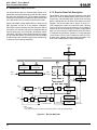
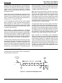
1
USER’S MANUAL
4
CHAPTER 4
DATA COMMUNICATION MODES
4.1 INTRODUCTION
The SCC provides two independent, full-duplex channels
programmable for use in any common asynchronous or
synchronous data communication protocol. The data communication protocols handled by the SCC are:
■
Asynchronous mode:
Asynchronous (x16, x32, or x64 clock
Isochronous (x1 clock)
■
Character-Oriented mode:
Monosynchronous
Bisynchronous
External Synchronous
■
Bit-Oriented mode
SDLC/HDLC
SDLC/HDLC Loop
4.1.1 Transmit Data Path Description
A diagram of the transmit data path is shown in Figure 4-1.
The transmitter has a Transmit Data buffer (a 4-byte deep
FIFO on the ESCC, a one byte deep buffer on the
NMOS/CMOS version) which is addressed through WR8.
It is not necessary to enable the transmit buffer. It is
available in all modes of operation. The Transmit Shift
register is loaded from either WR6, WR7, or the Transmit
Data buffer. In Synchronous modes, WR6 and WR7 are
programmed with the sync characters. In Monosync mode,
an 8-bit or 6-bit sync character is used (WR6), whereas a
16-bit sync character is used in the Bisynchronous mode
(WR6 and WR7). In bit-oriented Synchronous modes, the
SDLC flag character (7E hex) is programmed in WR7 and
is loaded into the Transmit Shift Register at the beginning
and end of each message.
Internal Data Bus
To Other Channel
TX Buffer (1-Byte; NMOS/CMOS)
TX FIFO (4 Byte; ESCC)
WR8
Internal TxD
WR7
WR6
SYNC Register
SYNC
Register
Final TX
MUX
20-Bit TX Shift Register
TxD
ASYNC
Zero
Insert
5-Bit Delay
SYNC
SDLC
Transmit
MUX & 2-Bit
Delay
NRZI
Encode
CRC-SDLC
Transmit Clock
CRC-Gen
From Receiver
Figure 4-1. Transmit Data Path
4-1
SCC™/ESCC™ User’s Manual
Data Communication Modes
4.1 INTRODUCTION (Continued)
For asynchronous data, the Transmit Shift register is formatted with start and stop bits along with the data; optionally with parity information bit. The formatted character is
shifted out to the transmit multiplexer at the selected clock
rate. WR6 & WR7 are not used in Asynchronous mode.
Synchronous data (except SDLC/HDLC) is shifted to the
CRC generator as well as to the transmit multiplexer.
SDLC/HDLC data is shifted to the CRC Generator and out
through the zero insertion logic (which is disabled while the
flags are being sent). A 0 is inserted in all address, control,
information, and frame check fields following five contiguous 1s in the data stream. The result of the CRC generator
for SDLC data is also routed through the zero insertion logic and then to the transmit multiplexer.
4.1.2 Receive Data Path Description
On the ESCC, the receiver has an 8-byte deep, 8-bit wide
Data FIFO, while the NMOS/CMOS version receiver has a
3-byte deep, 8-bit wide data buffer. In both cases, the Data
buffer is paired with an 8-bit Error FIFO and an 8-bit Shift
Register. The receive data path is shown in Figure 4-2.
This arrangement creates a 8-character buffer, allowing
time for the CPU to service an interrupt or for the DMA to
acquire the bus at the beginning of a block of high-speed
data. It is not necessary to enable the Receive FIFO, since
it is available in all modes of operation. For each data byte
in the Receive FIFO, a byte is loaded into the Error FIFO
to store parity, framing, and other status information. The
Error FIFO is addressed through Read Register 1.
CPU I/O
I/O Data buffer
Internal Data Bus
Upper Byte (WR13)
Time Constant
BRG
Input
Lower Byte (WR12)
Time Constant
16-Bit Down Counter
Status FIFO
10 x 19 Frame*
BRG
Output
DIV 2
See
Note
Rec. Data FIFO**
See
Note
14-Bit Counter
Rec. Error FIFO**
See
Note
Rec. Error Logic
Hunt Mode (BISYNC)
DPLL
IN
DPLL
OUT
DPLL
SYNC Register
& Zero Delete
3-Bit
Receive Shift
Register
Internal TXD
RxD
1-Bit
MUX
NRZI Decode
CRC Delay
Register (8 bits)
MUX
To Transmit Section
SDLC-CRC
CRC
Checker
Notes:
* Not with NMOS.
** Rec. Data FIFO and Rec. Error FIFO are 8 Bytes Deep (ESCC), 3 Bytes Deep (NMOS/CMOS).
Figure 4-2. Receive Data Path
4-2
SYNC
CRC
CRC Result
SCC™/ESCC™ User’s Manual
Data Communication Modes
Incoming data is routed through one of several paths depending on the mode and character length. In Asynchronous mode, serial data enters the 3-bit delay if a character
length of seven or eight bits is selected. If a character
length of five or six bits is selected, data enters the receive
shift register directly.
In Synchronous modes, the data path is determined by the
phase of the receive process currently in operation. A synchronous receive operation begins with a hunt phase in
which a bit pattern that matches the programmed sync
characters (6-,8-, or 16-bit) is searched.
The incoming data then passes through the Sync register
and is compared to a sync character stored in WR6 or
WR7 (depending on which mode it is in). The Monosync
mode matches the sync character programmed in WR7
and the character assembled in the Receive Sync register
to establish synchronization.
Synchronization is achieved differently in the Bisync
mode. Incoming data is shifted to the Receive Shift register
while the next eight bits of the message are assembled in
the Receive Sync register. If these two characters match
the programmed characters in WR6 and WR7, synchronization is established. Incoming data can then bypass the
Receive Sync register and enter the 3-bit delay directly.
The SDLC mode of operation uses the Receive Sync register to monitor the receive data stream and to perform zero
deletion when necessary; i.e., when five continuous 1s are
received, the sixth bit is inspected and deleted from the data
stream if it is 0. The seventh bit is inspected only if the sixth
bit equals one. If the seventh bit is 0, a flag sequence has
been received and the receiver is synchronized to that flag.
If the seventh bit is a 1, an abort or an EOP (End Of Poll) is
recognized, depending upon the selection of either the normal SDLC mode or SDLCLoop mode.
Note: The insertion and deletion of the zero in the SDLC
data stream is transparent to the user, as it is done after
the data is written to the Transmit FIFO and before data is
read from the Receive FIFO. This feature of the
SDLC/HDLC protocol is to prevent the inadvertent sending
of an ABORT sequence as part of the data stream. It is
also valuable to applications using encoded data to insure
a sufficient number of edges on the line to keep a DPLL
synchronized on a receive data stream.
The same path is taken by incoming data for both SDLC
and SDLC Loop modes. The reformatted data enters the
3-bit delay and is transferred to the Receive Shift register.
The SDLC receive operation begins in the hunt phase by
attempting to match the assembled character in the Receive Shift Register with the flag pattern in WR7. When the
flag character is recognized, subsequent data is routed
through the same path, regardless of character length.
Either the CRC-16 or CRC-SDLC (cyclic redundancy
check or CRC) polynomial can be used for both Monosync
and Bisync modes, but only the CRC-SDLC polynomial is
used for SDLC operation. The data path taken for each
mode is also different. Bisync protocol is a byte-oriented
operation that requires the CPU to decide whether or not a
data character is to be included in CRC calculation. An 8bit delay in all Synchronous modes except SDLC is allowed for this process. In SDLC mode, all bytes are included in the CRC calculation.
4.2 ASYNCHRONOUS MODE
In asynchronous communications, data is transferred in
the format shown in Figure 4-3.
Idle State
of Line
Stop
Bit(s)
Data Field
1
LSB
0
1
Start
Bit
Parity
Bit
1.5
2
Figure 4-3. Asynchronous Message Format
4-3
4
SCC™/ESCC™ User’s Manual
Data Communication Modes
4.2 ASYNCHRONOUS MODE (Continued)
The transmission of a character begins when the line
makes a transition from the 1 state (or MARK condition) to
the 0 state (or SPACE condition). This transition is the reference by which the character’s bit cell boundaries are defined. Though the transmitter and receiver have no common clock signal, they must be at the same data rate so
that the receiver can sample the data in the center of the
bit cell.
The SCC also supports Isochronous mode, which is the
same as Asynchronous except that the clock is the same
rate as the data. This mode is selected by selecting
x1 clock mode in WR4 (D7 & D6=0). Using this mode typically requires that the transmit clock source be transmitted
along with the data, or that the clock be synchronized with
the data.
The character can be broken up into four fields:
■
Start bit - signals the beginning of a character frame.
■
Data field - typically 5-8 bits wide.
■
Parity bit - optional error checking mechanism.
■
Stop bit(s) - Provides a minimum interval between the
end of one character and the beginning of the next.
Generation and checking of parity is optional and is controlled by WR4 D1 & D0. WR4 bit D0 is used to enable parity. If WR4 bit D1 is set, even parity is selected and if D1 is
reset, odd parity is selected. For even parity, the parity bit
is set/reset so that the data byte plus the parity bit contains
an even number of 1s. For odd parity, the parity bit is
set/reset such that the data byte plus the parity bit contains
an odd number of 1s.
The SCC supports Asynchronous mode with a number of
programmable options including the number of bits per
character, the number of stop bits, the clock factor, modem
interface signals, and break detect and generation.
Asynchronous mode is selected by programming the desired number of stop bits in D3 and D2 of WR4. Programming these two bits with other than 00 places both the receiver and transmitter in Asynchronous mode. In this
mode, the SCC ignores the state of bits D4, D3, and D2 of
WR3, bits D5 and D4 of WR4, bits D2 and D0 of WR5, all
4-4
of WR6 and WR7, and all of WR10 except D6 and D5. Ignored bits are programmed with 1 or 0 (Table 4-1).
Table 4-1. Write Register Bits Ignored in
Asynchronous Mode
Register
WR3
WR4
WR5
WR6
WR7
WR10
D7
D6
D5
x
x
x
x
x
x
x
x
D4
x
x
D3
x
D2
x
D1
0
x
x
x
x
x
x
x
x
x
x
x
x
x
D0
x
x
x
x
Note: If WR3 D1 is set (enabling the sync character load inhibit
feature), any character matching the value in WR6 is stripped out
of the incoming data stream and not put into the Receive FIFO.
Therefore, as this feature is typically only desired in synchronous
formats, this bit should reset in Asynchronous mode.
4.2.1 Asynchronous Transmit
Asynchronous mode is selected by specifying the number
of stop bits per character in bits D3 and D2 of WR4. The
three options available are one, one-and-a-half, and two
stop bits per character. These two bits select only the number of stop bits for the transmitter, as the receiver always
checks for one stop bit.
The number of bits per transmitted character is controlled
both by bits D6 and D5 in WR5 and the way the data is formatted within the transmit buffer (in the case of the ESCC,
Transmit FIFO). The bits in WR5 allow the option of five,
six, seven, or eight bits per character. In all cases the data
must be right-justified, with the unused bits being ignored
except in the case of five bits per character. When the five
bits per character option is selected, the data may be formatted before being written to the transmit buffer. This allows transmission of from one to five bits per character.
The formatting is shown in Table 4-2.
SCC™/ESCC™ User’s Manual
Data Communication Modes
Table 4-2. Transmit Bits per Character
Bit 7
Bit 6
0
1
0
1
0
0
1
1
5 or less bits/character
7 bits/character
6 bits/character
8 bits/character
Note: For five or less bits per character selection in WR5, the
following encoding is used in the data sent to the transmitter.
D is the data bit(s) to be sent.
D7
1
1
1
1
0
D6
1
1
1
0
0
D5
1
1
0
0
0
D4
1
0
0
0
D
D3
0
0
0
D
D
D2
0
0
D
D
D
D1
0
D
D
D
D
D0
D
D
D
D
D
Sends one data bit
Sends two data bits
Sends three data bits
Sends four data bits
Sends five data bits
An additional bit, carrying parity information, may be automatically appended to every transmitted character by setting bit D0 of WR4 to 1. This bit is sent in addition to the
number of bits specified in WR4 or by bit D1 of WR4. If this
bit is set to 1, the transmitter sends even parity and, if set
to 0, the parity is odd.
The transmitter may be programmed to send a Break by
setting bit D4 of WR5 to 1. The transmitter will send contiguous 0s from the first transmit clock edge after this command is issued, until the first transmit clock edge after this
bit is reset. The transmit clock edges referred to here are
those that defined transmitted bit cell boundaries. Care
must be taken when Break is sent. As mentioned above,
the SCC initiates the Break sequence regardless of the
character boundaries. Typically, the break sequence is defined as “null character (all 0 data) with framing error”. The
other party may not be able to recognize it as a break sequence if the Send Break bit has been set in the middle of
sending a non-zero character.
An additional status bit for use in Asynchronous mode is
available in bit D0 of RR1. This bit, called All Sent, is set
when the transmitter is completely empty and any previous
data or stop bits have reached the TxD pin. The All Sent
bit can be used by the processor as an indication that the
transmitter may be safely disabled, or indication to change
the modem status signal.
The SCC may be programmed to accept a transmit clock
that is one, sixteen, thirty-two, or sixty-four times the data
rate. This is selected by bits D7 and D6 in WR4, in common with the clock factor for the receiver.
Note: When using Isosynchronous (X1 clock) mode, oneand-a-half stop bits are not allowed. Only one or two stop
bits should be selected. If some length other than one stop
bit is desired in the times one mode, only two stop bits may
be used. Also, in this mode, the Transmitter usually needs
to send clocking information (transmit clock) along with the
data in order to receive data correctly.
There are two modem control signals associated with the
transmitter provided by the SCC; /RTS and /CTS.
The /RTS pin is a simple output that carries the inverted
state of the RTS bit (D1) in WR5, unless the Auto Enables
mode bit (D5) is set in WR3. When Auto Enables is set, the
/RTS pin immediately goes Low when the RTS bit is set.
However, when the RTS bit is reset, the /RTS pin remains
Low until the transmitter is completely empty and the last
stop bit has left the TxD pin. Thus, the /RTS pin may be
used to disable external drivers for the transmit data. The
/CTS pin is ordinarily a simple input to the CTS bit in RR0.
However, if Auto Enables mode is selected, this pin becomes an enable for the transmitter. That is, if Auto Enables is on and the /CTS pin is High, the transmitter is disabled; the transmitter is enabled while the /CTS pin is Low.
The initialization sequence for the transmitter in Asynchronous mode is WR4 first to select the mode, then WR3 and
WR5 to select the various options. At this point the other
registers should be initialized as necessary. When all of
this is complete, the transmitter may be enabled by setting
bit D3 of WR5 to 1. Note that the transmitter and receiver
may be initialized at the same time.
4.2.1.1 Asynchronous transmit on the NMOS/CMOS
On the NMOS/CMOS version of the SCC, characters are
loaded from the transmit buffer to the shift register where
they are given a start bit and a parity bit (as programmed),
and are shifted out to the TxD pin. The transmit buffer
empty interrupt and the DMA request (either /W//REQ or
/DTR//REQ pin) are asserted when the transmit buffer is
empty, if these are enabled. At this time, the CPU or the
DMA is able to write one byte of transmit data. The Transmit Buffer Empty (TBE) bit (RR0, bit D2) also follows the
state of the transmit buffer. The All Sent bit, RR1, bit D0,
can be polled to determine when the last bit of transmit
data has cleared the TxD pin. For details about the transmit DMA and transmit interrupts, refer to Section 2.4.8
“Transmit Interrupt and Transmit Buffer Empty bit.”
4.2.1.2 Asynchronous transmit on the ESCC
On the ESCC, characters are loaded from the Transmit
FIFO to the shift register where they are given a start bit
and a parity bit (as programmed), and are shifted out to the
TxD pin. The ESCC can generate an interrupt or DMA request depending on the status of the Transmit FIFO. If
WR7' D5 is reset, the transmit buffer empty interrupt and
DMA request (either /W//REQ or /DTR//REQ pin) are asserted when the entry location of the Transmit FIFO is
empty (one byte can be written). If WR7' D5 is set, the
transmit interrupt and DMA request is generated when the
Transmit FIFO is completely empty (four bytes can be written). The Transmit Buffer Empty (TBE) bit in RR0, bit D2
also is affected by the state of WR7' bit D5. The All Sent
4-5
4
SCC™/ESCC™ User’s Manual
Data Communication Modes
4.2 ASYNCHRONOUS MODE (Continued)
bit, bit D0 of RR1, can be polled to determine when the last
bit of transmit data has cleared the TxD pin.
■
Parity errors—The parity bit of a character disagrees
with the sense programmed in WR4.
The number of transmit interrupts can be minimized by setting bit D5 of WR7' to one and writing four bytes to the
transmitter for each transmit interrupt. This requires that
the system response to interrupt is less than the time it
takes to transmit one byte at the programmed baud rate. If
the system’s interrupt response time is too long to use this
feature, bit D5 of WR7' should be reset to 0. Then, poll the
TBE bit and poll after each data write to test if there is
space in the Transmit FIFO for more data.
■
Overrun errors—When the Receive FIFO overflows.
For details about the transmit DMA and transmit interrupts,
refer to Section 2.4.8 “Transmit Interrupt and Transmit
Buffer Empty bit”.
4.2.2 Asynchronous Receive
Asynchronous mode is selected by specifying the number
of stop bits per character in bits D3 and D2 of WR4. This
selection applies only to the transmitter, however, as the
receiver always checks for one stop bit. If after character
assembly the receiver finds this stop bit to be a 0, the
Framing Error bit in the receive error FIFO is set at the
same time that the character is transferred to the receive
data FIFO. This error bit accompanies the data to the exit
location (CPU side) of the Receive FIFO, where it is a special receive condition. The Framing Error bit is not latched,
so it must be read in RR1 before the accompanying data
is read.
The number of bits per character is controlled by bits D7
and D6 of WR3. Five, six, seven or eight bits per character
may be selected via these two bits. Data is right justified
with the unused bits set to 1s. An additional bit, carrying
parity information, may be selected by setting bit D0 of
WR4 to 1. Note that this also enables parity for the transmitter. The parity sense is selected by bit D1 of WR4. If this
bit is set to 1, the received character is checked for even
parity, and if set to 0, the received character is checked for
odd parity. The additional bit per character that is parity is
transferred to the receive data FIFO along with the data, if
the data plus parity is eight bits or less. The parity error bit
in the receive error FIFO may be programmed to cause
special receive interrupts by setting bit D2 of WR1 to 1.
Once set, this error bit is latched and remains active until
an Error Reset command has been issued.
Since errors apply to specific characters, it is necessary
that error information moves alongside the data that it refers to. This is implemented in the SCC with an error FIFO
in parallel with the data FIFO. The three error conditions
that the receiver checks for in Asynchronous mode are:
■
4-6
Framing errors—When a character’s stop bit is a 0.
If interrupts are not used to transfer data, the Parity Error,
Framing Error, and Overrun Error bits in RR1 should be
checked before the data is removed from the receive data
FIFO, because reading data pops up the error information
stored in the Error FIFO.
The SCC may be programmed to accept a receive clock
that is one, sixteen, thirty-two, or sixty-four times the data
rate. This is selected by bits D7 and D6 in WR4. The 1X
mode is used when bit synchronization external to the received clock is present (i.e., the clock recovery circuit, or
active receive clock from the sender side). The 1X mode is
the only mode in which a data encoding method other than
NRZ may be used. The clock factor is common to the receiver and transmitter.
The break condition is continuous 0s, as opposed to the
usual continuous ones during an idle condition. The SCC
recognizes the Break condition upon seeing a null character (all 0s) plus a framing error. Upon recognizing this sequence, the Break bit in RR0 is set and remains set until a
1 is received. At this point, the break condition is no longer
present. At the termination of a break, the receive data
FIFO contains a single null character, which should be
read and discarded. The framing error bit will not be set for
this character, but if odd parity has been selected, the Parity Error bit is set.
Note: Caution should be exercised if the receive data line
contains a switch that is not debounced to generate
breaks. If this is the case, switch bounce may cause multiple breaks to be recognized by the SCC, with additional
characters assembled in the receive data FIFO and the
possibility of a receive overrun condition being latched.
The SCC provides up to three modem control signals associated with the receiver; /SYNC, /DTR//REQ,
and /DCD.
The /SYNC pin is a general purpose input whose state is
reported in the Sync/Hunt bit in RR0. If the crystal oscillator
is enabled, this pin is not available and the Sync/Hunt bit
is forced to 0. Otherwise, the /SYNC pin may be used to
carry the Ring Indicator signal.
The /DTR//REQ pin carries the inverted state of the DTR
bit (D7) in WR5 unless this pin has been programmed to
carry a DMA request signal.
The /DCD pin is ordinarily a simple input to the DCD bit in
RR0. However, if the Auto Enables mode is selected by
setting D5 of WR3 to 1, this pin becomes an enable for the
SCC™/ESCC™ User’s Manual
Data Communication Modes
receiver. That is, if Auto Enables is on and the /DCD pin is
High, the receiver is disabled; while the /DCD pin is low,
the receiver is enabled.
Received characters are assembled, checked for errors,
and moved to the receive data FIFO (eight bytes on ESCC,
three bytes on NMOS/CMOS). The user can program the
SCC to generate an interrupt to the CPU or to request a
data read from a DMA when data is received.
On the NMOS/CMOS version, it generates the Receive
Character Available interrupt and DMA Request on Receive (if enabled). The receive interrupt and DMA request
is generated when there is at least one character in the
FIFO. The Rx Character Available (RCA) bit is set if there
is at least one byte available.
The ESCC generates the receive character available interrupt and DMA request on Receive (if enabled) and is dependent on WR7' bit D3. If this bit is reset to 0 (this mode
is comparable to the NMOS/CMOS version), the receive
interrupt and DMA request is generated when there is at
least one character in the FIFO. If WR7' bit D3 is set to 1,
the receive interrupt and DMA request are generated
when there are four bytes available in the Receive FIFO.
The RCA bit in RR0 follows the state of WR7' D3. The RCA
bit is set if there is at least one byte available, regardless
of the status of WR7' bit D3.
This is the initialization sequence for the receiver in Asynchronous mode. First, WR4 selects the mode, then WR3
and WR5 select the various options. At this point, the other
registers should be initialized as necessary. When all of
this is complete, the receiver may be enabled by setting bit
D0 of WR3 to 1.
4.2.3 Asynchronous Initialization
The initialization sequence for Asynchronous mode is
shown in Table 4-3. All of the SCC’s registers should be reinitialized after a channel or hardware reset. Also, WR4
should be programmed first after a reset.
Table 4-3. Initialization Sequence
Asynchronous Mode
Reg
Bit No Description
WR9
WR4
6, 7
3, 2
WR3
0, 1
6, 7
7, 6
WR5
5
6, 5
1
Hardware or channel Reset
Select Async Mode and the number
of stop bits*
Select parity*
Select clock mode*
Select number of receive bits per
character
Select Auto Enables Mode*
Select number of bits/char for
transmitter
Select modem control (RTS)
Note:
* Initializes transmitter and receiver simultaneously.
At this point, the other registers should be initialized according to the hardware design such as clocking,
I/O mode, etc. When this is completed, the transmitter is
enabled by setting WR5 bit D3 to 1 and the receiver is enabled by setting WR3 bit D0 to 1.
See Section 2.4.7 “The Receive Interrupt” for more details
on receive interrupts.
4-7
4
SCC™/ESCC™ User’s Manual
Data Communication Modes
4.3 BYTE-ORIENTED SYNCHRONOUS MODE
The SCC supports three byte-oriented synchronous protocols. They are: monosynchronous, bisynchronous, and external synchronous.
with no gaps between characters. This requires that there
be an agreement as to the location of the character
boundaries so that the characters can be properly
framed. This is normally accomplished by defining special synchronization patterns, or Sync characters. The
synchronization pattern serves as a reference; it signals
the receiver that a character boundary occurs immediately after the last bit of the pattern. For example Monosync
Protocol usually uses 16 Hex as this special character,
and the SDLC protocol uses 0, six 1s, followed by a 0 (7E
Hex; usually referred to as Flag Pattern) to mark the beginning and end of a block of data. Another way of identifying the character boundaries (i.e., achieving synchronization) is with a logic signal that goes active just as the
first character is about to enter the receiver. This method
is referred to as External Synchronization.
In synchronous communications, the bit cell boundaries
are referenced to a clock signal common to both the transmitter and receiver. Consequently, they operate in a fixedphase relationship. This eliminates the need for the receiver to locate the bit cell boundaries with a clock 16, 32, or
64 times the receive data rate, allowing for higher speed
communication links. Some applications may encode (i.e.,
NRZI or FM coding) the clock information on the same line
as the data. Therefore, these applications require that the
receiver use a high speed clock to find the bit cell boundaries (decoding is typically done with the PLL—PhaseLocked Loop; the SCC has on-chip Digital PLL). Data encoding eliminates the need to transmit the synchronous
clock on a separate wire from the data.
Figure 4-4 shows the character format for synchronous
transmission. For example, bits 1-8 might be one character and bits 9-13 part of another character; or, bit 1 might
be part of a second character, and bits 10-13 part of a third
character. This is accomplished by defining a synchronization character, commonly called a Sync Character.
Synchronous data does not use start and stop bits to delineate the boundaries for each character. This eliminates
the overhead associated with every character and increases the line efficiency. Because of the phase relationship of
synchronous data to a clock, data is transferred in blocks
1 Bit Time
Modem Clock
Bit
1
2 3 4
5 6
Bit State
0
1 1 0
1 0
Data
LSB
7 8
0 0
Sync Character
9 10 11 12 13 . . .
1 1
0 1
0 1
0 1
Data Character
Figure 4-4. Monosync Data Character Format
4.3.1 Byte-Oriented Synchronous Transmit
Once Synchronous mode has been selected, any of three
of the following sync character lengths may be selected:
■
6-bit
■
8-bit
■
16-bit
The 6-bit option sync character is selected by setting bits
4 and 5 of WR4 to zeros and bit 0 of WR10 to one. Only
the least significant six bits of WR6 are transmitted.
4-8
The 8-bit sync character is selected by setting bits 4 and 5
of WR4 to zeros and bit 0 of WR10 to zeros. With this option selected, the transmitter sends the contents of WR6
when it has no data to send.
For a 16-bit sync character, set bit D4 of WR4 to 1 and bit
D5 of WR4 and bit D0 of WR10 to 0. In this mode, the
transmitter sends the concatenation of WR6 and WR7 for
the idle line condition.
Because the receiver requires that sync characters be leftjustified in the registers, while the transmitter requires
them to be right justified, only the receiver works with a 12bit sync character. While the receiver is in External Sync
SCC™/ESCC™ User’s Manual
Data Communication Modes
mode, the transmitter sync length may be six or eight bits,
as selected by bit D0 of WR10.
Monosync and Bisync modes require clocking information
to be transmitted along with the data either by a method of
encoding data that contains clocking information, or by a
modem that encodes or decodes clock information in the
modulation process. Refer to the Monosync message format shown in Figure 4-4.
The Bisync mode of operation is similar to the Monosync
mode, except that two sync characters are provided instead of one. Bisync attempts a more structured approach
to synchronization through the use of special characters
as message headers or trailers.
Character-oriented mode is selected by programming bits
D3 and D2 of WR4 with zeros. This selects Synchronous
mode, as opposed to Asynchronous mode, but this selection is further modified by bits 5 and 7 of WR4 as well as
bits 1 and 0 of WR10. During the sync character-oriented
modes, except in External Sync mode, the state of bits 7
and 6 of WR4 are always forced internally to zeros. In external sync mode, these two bits must be programmed with
zeros (Table 4-4.). The combination, other than 00 in External Sync mode, puts the SCC in special synchronization
modes.
Table 4-4. Registers Used in Character-Oriented
Modes
Reg
WR4
WR6
WR7
WR10
Bit No
3 (=0)
2 (=0)
4 (=0)
5 (=0)
4 (=1)
5 (=0)
4 (=1)
5 (=1)
6 (=0)
7 (=0)
7-0
7-0
1
Description
select sync mode
select monosync mode
(8-bit sync character)
select bisync mode
(16-bit sync character)
select external sync mode
(external sync signal required)
select 1x clock mode
sync character (low byte)
sync character (high byte)
select sync character length
In character-oriented modes, a special bit pattern is used
to provide character synchronization. The SCC offers several options to support Synchronous mode including various sync generation and checking, CRC generation and
checking, as well as modem controls and a transmitter to
receiver synchronization function.
The number of bits per transmitted character is controlled
by D6 and D5 of WR5 plus the way the data is formatted
within the transmit buffer. The bits in WR5 select the option
of five, six, seven, or eight bits per character. In all cases,
the data must be right-justified, with the unused bits being
ignored except in the case of five bits per character. When
the five bits per character option is selected, the data must
be formatted before being written to the transmit buffer to
allow transmission of from one to five bits per character.
This formatting is shown in Table 4-2.
An additional bit, carrying parity information, may be automatically appended to every transmitted character by setting bit D0 of WR4 to 1. This parity bit is sent in addition to
the number of bits specified in WR4 or by the data format.
If this bit is set to 1, the transmitter sends even parity; if set
to 0, the transmitted parity is odd. Parity is not typically
used in synchronous applications because the CRC provides a more reliable method for detecting errors.
Either of two CRC polynomials are used in Synchronous
modes, selected by bit D2 in WR5. If this bit is set to 1, the
CRC-16 polynomial is used and, if this bit is set to 0, the
CRC-CCITT polynomial is used. This bit controls the selection for both the transmitter and receiver. The initial
state of the generator and checker is controlled by bit D7
of WR10. When this bit is set to 1, both the generator and
checker have an initial value of all ones; if this bit is set to
0, the initial values are all zeros.
The SCC does not automatically preset the CRC generator in byte Synchronous modes, so this must be done in
software. This is accomplished by issuing the Reset Tx
CRC Generator command, which is encoded in bits D7
and D6 of WR0. For proper results, this command is issued while the transmitter is enabled and sending sync
characters.
If the CRC is to be used, the transmit CRC generator must
be enabled by setting bit D0 of WR5 to 1. This bit may also
be used to exclude certain characters from the CRC calculation. Sync characters (from sync registers) are automatically excluded from the CRC calculation, and any characters written as data are excluded from the calculation by
using bit D0 of WR5. Internally, enabling or disabling the
CRC for a particular character happens at the same time
the character is loaded from the transmit data buffer (on
the ESCC, the Transmit FIFO) to the Transmit Shift register. Thus, to exclude a character from the CRC calculation
bit, D0 of WR5 is set to 0 before the character is written to
the transmit buffer (on the ESCC, the Transmit FIFO).
ESCC:
Since the ESCC has a four-byte FIFO, if a character is
to be excluded from the CRC calculation, it is recommended that only one byte be written to the ESCC at
that time. If WR7' D5 is reset, the transmit interrupt is
generated when the FIFO is completely empty. This
can be used as a signal to reset WR5 bit D0, and then
the character can be written to the Transmit FIFO. This
guarantees that the internal disable occurs when the
character moves from the buffer to the shift register.
4-9
4
SCC™/ESCC™ User’s Manual
Data Communication Modes
4.3 BYTE-ORIENTED SYNCHRONOUS MODE (Continued)
Once the buffer becomes empty, the Tx CRC Enable
bit is written for the next character.
The initialization sequence for the transmitter in characteroriented mode is shown in Table 4-5.
Enabling the CRC generator is not sufficient to control the
transmission of the CRC. In the SCC, this function is controlled by the Tx Underrun/EOM bit, which is reset by the
processor and set by the SCC. When the transmitter underruns (both the transmit buffer and Transmit Shift register are empty) the state of the Tx Underrun/EOM bit determines the action taken by the SCC. If the Tx
Underrun/EOM bit is reset when the underrun occurs, the
transmitter sends the accumulated CRC and sets the Tx
Underrun/EOM bit to indicate this. This transition is programmed to cause an external/status interrupt, or the Tx
Underrun/EOM is available in RR0.
Table 4-5. Transmitter Initialization in CharacterOriented Mode
The Reset Tx Underrun/EOM Latch command is encoded
in bits D7 and D6 of WR0. For correct transmission of the
CRC at the end of a block of data, this command is issued
after the first character is written to the SCC but before the
transmitter underruns. The command is usually issued immediately after the first character is written to the SCC so
that the CRC is sent if an underrun occurs inadvertently
during the block of data.
85X30
If WR7' bit D1 is set, the Reset Transmit Underrun/EOM
latch is automatically reset after the first byte is written to the transmitter. This eliminates the need for the
CPU to issue this command. This feature can be particularly useful to applications using a DMA to write
data to the transmitter since there is no longer a need
to interrupt the data transfers to issue this command.
If the transmitter is disabled during the transmission of a
character, that character is sent completely. This applies
to both data and sync characters. However, if the transmitter is disabled during the transmission of the CRC, the
16-bit transmission is completed, but the remaining bits
will come from the Sync registers rather than the remainder of the CRC.
There are two modem control signals associated with the
transmitter provided by the SCC: /RTS and /CTS.
The /RTS pin is a simple output that carries the inverted
state of the RTS bit (D1) in WR5.
The /CTS pin is ordinarily a simple input to the CTS bit in
RR0. However, if Auto Enables mode is selected, this pin
becomes an enable for the transmitter. That is, if Auto Enables is on and the /CTS pin is High, the transmitter is disabled. While the /CTS pin is Low, the transmitter is enabled.
4-10
Reg
WR4
Bit No
0,1
WR5
1
2
5,6
7
WR10
Description
selects parity (not typically used
insync modes)
RTS
selects CRC generator
selects number of bits per character
CRC preset value
At this point, the other registers should be initialized as necessary. When all of this is completed, the transmitter is enabled by setting bit 3 of WR5 to one. Now that the transmitter is enabled, the CRC generator is initialized by issuing the
Reset Tx CRC Generator command in WR0, bits 6-7.
4.3.2 Byte-Oriented Synchronous Receive
The receiver in the SCC searches for character synchronization only while it is in Hunt mode. In this mode the receiver is idle except that it is searching the incoming data
stream for a sync character match.
In Hunt mode, the receiver shifts for each bit into the Receive Shift register. The contents of the Receive Shift register are compared with the sync character (stored in another register), repeating the process until a match occurs.
When a match occurs, the receiver begins transferring
bytes to the Receive FIFO.
The receiver is in Hunt mode when it is first enabled, and
it may be placed in Hunt mode by the processor issuing the
Enter Hunt Mode command in WR3. This bit (D4) is a command, so writing a 0 to it has no effect. The hunt status of
the receiver is reported by the Sync/Hunt bit in RR0.
Sync/Hunt is one of the possible sources of external/status
interrupts, with both transitions causing an interrupt. This
is true even if the Sync/Hunt bit is set as a result of the processor issuing the Enter Hunt Mode command.
Once the sync character-oriented mode has been selected, any of the four sync character lengths may be selected:
6 bits, 8 bits, 12 bits, or 16 bits.
The Table 4-6 shows the write register bit setting for selecting sync character length.
SCC™/ESCC™ User’s Manual
Data Communication Modes
Table 4-6. Sync Character Length Selection
Sync Length
6 bits
8 bits
12 bits
16 bits
WR4,D5
0
0
0
0
WR4,D4
0
0
1
1
provide a character synchronization signal on the /SYNC
pin. This mode is selected by setting bits D5 and D4 of
WR4 to 1. In this mode, the Sync/Hunt bit in RR0 reports
the state of the /SYNC pin, but the receiver is still placed in
Hunt mode when the external logic is searching for a sync
character match. Two receive clock cycles after the last bit
of the sync character is received, the receiver is in Hunt
mode and the /SYNC pin is driven Low, then character assembly begins on the rising edge of the receive clock. This
immediately precedes the activation of /SYNC (Figure 46). The receiver leaves Hunt mode when /SYNC is driven
Low.
WR10,D0
1
0
1
0
The arrangement of the sync character in WR6 and WR7
is shown in Figure 4-5.
For those applications requiring any other sync character
length, the SCC makes provision for an external circuit to
Write Register 6
D7 D6 D5 D4 D3 D2 D1 D0
Sync7
Sync1
Sync7
Sync3
ADR7
ADR7
Sync6
Sync0
Sync6
Sync2
ADR6
ADR6
Sync5
Sync5
Sync5
Sync1
ADR5
ADR5
Sync4
Sync4
Sync4
Sync0
ADR4
ADR4
Sync3
Sync3
Sync3
1
ADR3
x
Sync2 Sync1
Sync2 Sync1
Sync2 Sync1
1
1
ADR2 ADR1
x
x
Sync0
Sync0
Sync0
1
ADR0
x
Monosync, 8 Bits
Monosync, 6 Bits
Bisync, 16 Bits
Bisync, 12 Bits
SDLC
SDLC (Address Range)
Write Register 7
D7 D6 D5 D4 D3 D2 D1 D0
Sync7
Sync5
Sync15
Sync11
0
Sync6
Sync4
Sync14
Sync10
1
Sync5
Sync3
Sync13
Sync9
1
Sync4
Sync2
Sync12
Sync8
1
Sync3
Sync1
Sync11
Sync7
1
Sync2 Sync1 Sync0 Monosync, 8 Bits
Sync0
x
x
Monosync, 6 Bits
Sync10 Sync9 Sync8 Bisync, 16 Bits
Sync6 Sync5 Sync4 Bisync, 12 Bits
1
1
0
SDLC
Figure 4-5. Sync Character Programming
/RTxC
RxD
SYNC Last-1
SYNC Last
Data 0
Data 1
Data 2
/SYNC
Figure 4-6. /SYNC as an Input
4-11
4
SCC™/ESCC™ User’s Manual
Data Communication Modes
4.3 BYTE-ORIENTED SYNCHRONOUS MODE (Continued)
In all cases except External Sync mode, the /SYNC pin is
an output that is driven Low by the SCC to signal that a
sync character has been received. The /SYNC pin is
activated regardless of character boundaries, so any
external circuitry using it should only respond to the /SYNC
pulse that occurs while the receiver is in Hunt mode. The
timing for the /SYNC signal is shown in Figure 4-7.
/RTxC
PCLK
/SYNC
State Changes in One
/RTxC Clock Cycle
Figure 4-7. /SYNC as an Output
To prevent sync characters from entering the receive data
FIFO, set the Sync Character Load Inhibit bit (D1) in WR3
to 1. While this bit is set to 1, characters about to be loaded
into the receive data FIFO are compared with the contents
of WR6. If all eight bits match the character, it is not loaded
into the receive data FIFO. Because the comparison is
across eight bits, this function should only be used with 8bit sync characters. It cannot be used with 12- or 16-bit
sync characters. Both leading sync characters are removed in the case of a 6-bit sync character. Care must be
exercised in using this feature because sync characters
which are not transferred to the receive data FIFO will automatically be excluded from CRC calculation. This works
properly only in the 8-bit case.
The number of bits per character is controlled by bits D7
and D6 of WR3. Five, six, seven, or eight bits per character
may be selected via these two bits. The data is right-justified in the receive data buffer. The SCC merely takes a
snapshot of the receive data stream at the appropriate
times, so the “unused” bits in the receive buffer are only
the bits following the character in the data stream.
4-12
An additional bit carrying parity information is selected by
setting bit D0 of WR4 to 1. Note that this also enables parity for the transmitter. The bit D1 of WR4 selects parity
sense. If this bit is set to 1, the received character is
checked for even parity. If WR4 D1 is reset to 0, the received character is checked for odd parity. The additional
bit per character is transferred to the FIFO as a part of data
when the data plus parity is less than 8 bits per character.
The Parity Error bit in the receive error FIFO may be programmed to cause a Special Receive Condition interrupt
by setting bit D2 of WR1 to 1. Once set, this error bit is
latched and remains active until an Error Reset command
has been issued. If interrupts are not used to transfer data,
the Parity Error, CRC Error, and Overrun Error bits in RR1
should be checked before the data is removed from the receive data FIFO.
The character length can be changed at any time before
the new number of bits has been assembled by the
receiver, but, care should be exercised as unexpected
results may occur. A representative example would be
switching from five bits to eight bits and back to five bits
(Figure 4-8).
SCC™/ESCC™ User’s Manual
Data Communication Modes
Receive Data Buffer
Time
4
3
2
1
5 Bits
13 12 11 10 9
8
7
6
8 Bits
21 20 19 18 17 16 15 14
8 Bits
29 28 27 26 25 24 23 22
5 Bits
34 33 32 31 30 29 28 27
5 Bits
8
7
6
5
4
Change from Five to Eight
Change from Eight to Five
39 38 37 36 35 34 33 32
Figure 4-8. Changing Character Length
Either of two CRC polynomials are used in Synchronous
modes, selected by bit D2 in WR5. If this bit is set to 1, the
CRC-16 polynomial is used, if this bit is set to 0, the CRCCCITT polynomial is used. This bit controls the polynomial
selection for both the receiver and transmitter.
The initial state of the generator and checker is controlled
by bit D7 of WR10. When this bit is set to 1, both the generator and checker have initial values of all ones; if this bit
is set to 0, the initial values are all 0. The SCC presets the
checker whenever the receiver is in Hunt mode so a CRC
reset command is not necessary. However, there is a Reset CRC Checker command in WR0. This command is encoded in bits D7 and D6 of WR0. If the CRC is used, the
CRC checker is enabled by setting bit D0 of WR3 to 1.
Sync characters can be stripped from the data stream any
time before the first non-sync character is received. If the
sync strip feature is not being used, the CRC is not enabled until after the first data character has been transferred to the receive data FIFO. As previously mentioned,
8-bit sync characters stripped from the data stream are automatically excluded from CRC calculation.
Some synchronous protocols require that certain characters be excluded from CRC calculation. This is possible in
the SCC because CRC calculations are enabled and disabled on the fly. To give the processor sufficient time to decide whether or not a particular character should be included in the CRC calculation, the SCC contains an 8-bit time
delay between the receive shift register and the CRC
checker. The logic also guarantees that the calculation
only starts or stops on a character boundary by delaying
the enable or disable until the next character is loaded into
the receive data FIFO. Because the nature of the protocol
requires that CRC calculation disable/enable be selected
before the next character gets loaded into the Receive
FIFO, users cannot take advantage of the FIFO.
To understand how this works refer to Figure 4-9 and the
following explanation. Consider a case where the SCC
receives a sequence of eight bytes, called A, B, C, D, E, F,
G and H, with A received first. Now suppose that A is the
sync character, the CRC is calculated on B, C, E, and F,
and that F is the last byte of this message. This process is
used to control the SCC.
4-13
SCC™/ESCC™ User’s Manual
Data Communication Modes
4.3 BYTE-ORIENTED SYNCHRONOUS MODE (Continued)
3 Bytes Deep for NMOS/CMOS
8 Bytes Deep for ESCC
Receive Data FIFO
Receive Data
Receive Shift Register
Eight Bit Time Delay
CRC Checker
Figure 4-9. Receive CRC Data Path
Before A is received, the receiver is in Hunt mode and the
CRC is disabled. When A is in the receive shift register, it
is compared with the contents of WR7. Since A is the sync
character, the bit patterns match and receive leaves Hunt
mode, but character A is not transferred to the receive
data FIFO.
After eight-bit times, B is loaded into the receive data
FIFO. The CRC remains disabled even though somewhere during the next eight bit times the processor reads
B and enables the CRC. At the end of this eight-bit time, B
is in the 8-bit delay and C is in the receive shift register.
Character C is loaded into the receive data FIFO and at the
same time the CRC checker becomes enabled. During the
next eight-bit time, the processor reads C and since the
CRC is enabled within this period, the SCC has calculated
the CRC on B, character C is the 8-bit delay, and D is in
the Receive Shift register. D is then loaded into the receive
data FIFO and at some point during the next eight-bit time
the processor reads D and disables the CRC. At the end
of these eight-bit times, the CRC has been calculated on
C, character D is in the 8-bit delay, and E is in the Receive
Shift register.
Now E is loaded into the receive data FIFO. During the
next eight-bit time, the processor reads E and enables the
CRC. During this time E shifts into the 8-bit delay, F enters
4-14
the Receive Shift register and the CRC is not being calculated on D. After these eight-bit times have elapsed, E is in
the 8-bit delay, and F is in the Receive Shift register. Now
F is transferred to the receive data FIFO and the CRC is
enabled. During the next eight-bit times, the processor
reads F and leaves the CRC enabled. The processor detects that this is the last character in the message and prepares to check the result of the CRC computation. However, another sixteen bit-times are required before the CRC
has been calculated on all of character F.
At the end of eight-bit times, F is in the 8-bit delay and G is
in the Receive Shift register. At this time, it is transferred to
the receive data FIFO. Character G is read and discarded
by the processor. Eight-bit times later, H is also transferred
to the receive data FIFO. The result of a CRC calculation
is latched in to the Receive Error FIFO at the same time as
data is written to the Receive Data FIFO. Thus, the CRC
result through character F accompanies character H in the
FIFO and will be valid in RR1 until character H is read from
the Receive Data FIFO. The CRC checker is disabled and
reset at any time after character H is transferred to the Receive Data FIFO. Recall, however, that internally the CRC
is not disabled until after this occurs. A better alternative is
to place the receiver in Hunt mode, which automatically
disables and resets the CRC checker. See Table 4-7 for a
condensed description.
SCC™/ESCC™ User’s Manual
Data Communication Modes
Modem Controls. Up to two modem control signals associated with the receiver are available in Synchronous
modes: /DTR//REQ and /DCD. The /DTR//REQ pin carries
the inverted state of the DTR bit (D7) in WR5 unless this
pin has been programmed to carry a DMA Request on
Transmit signal. The /DCD pin is ordinarily a simple input
to the DCD bit in RR0. However, if the Auto Enables mode
is selected by setting D5 of WR3 to 1, this pin becomes an
enable for the receiver. Therefore, if Auto Enables is ON
and the /DCD pin is High, the receiver is disabled; while
the /DCD pin is Low, the receiver is enabled.
Initialization. The initialization sequence for the receiver
in character-oriented mode is WR4 first, to select the
mode, then WR10 to modify it if necessary; WR6 and WR7
to program the sync characters; WR3 and WR5 to select
the various options. At this point the other registers are initialized as necessary. When all this is completed, the receiver is enabled by setting bit D0 of WR3 to a one. A summary is shown in Table 4-8. A detailed example of using
the SCC in 16-bit sync mode is available in the application
note “SCC in Binary Synchronous Communications.”
Note that with Auto Enables mode enabled, when /DCD
goes inactive, the receiver stops immediately and the
character being assembled is lost.
4-15
4
SCC™/ESCC™ User’s Manual
Data Communication Modes
4.3 BYTE-ORIENTED SYNCHRONOUS MODE (Continued)
Table 4-7. Enabling and Disabling CRC
A
B
C
D
E
F
(Sync) (Data1) (Data2) (Data3) (CRC1) (CRC2)
G
H
(Data)
(Data)
Note: No CRC Calculation on "D"
Stage
1
Direction of Data
Coming into SCC
Receive
Delay
Data FIFO Register
HGFEDCB
HGFEDC
2
Shift
Register
HGFEDC
CRC
Notes
d
A
d
B
CPU Read
B
d
CPU Enables CR
3
HGFED
C
CPU Read
HGFE
CPU Read
B
e
C
e
D
d
E
e
F
e
G
e
C
D
CRC Calc on B
D*
CPU Disables CR
4
HGF
CPU Read
E
E
CPU Enables CR
5
HG
CPU Read
F
H
G
CRC Calc is
Disabled on D
F
CPU Reads & Disca
CRC Calc on E
G
H
Read RR1 D
H
Read H & Disca
H
Legend:
* Usually D is a end-of-message character indicator.
† The status is latched on the Error FIFO for each received byte. In the calculation of F,
the CRC error flag in the Error FIFO will be 0 for an error free message.
d = disabled
e = enabled
ABCDEFGH
A = SYNC
B - F = Data with E = CRC1 and F = CRC2
G and H are arbitrary data (Pad Character)
4-16
CRC Calc on C
CRC Calc on F
CRC Calc on F
Result latched in
Error FIFO †
SCC™/ESCC™ User’s Manual
Data Communication Modes
Table 4-8. Initializing the Receiver in Character-Oriented Mode
Bit Number
Reg
WR4
4
D7
0
D6
0
D5
0
D4
x
D3
0
D2
0
D1
0
D0 Description
0 Select x1 clock, enable sync mode, & no parity
x=0 for 8-bit sync, x=1 for 16-bit sync
WR3
r
x
0
1
1
0
0
0
rx=# of Rx bits/char, No auto enable, enter Hunt,
Enable Rx CRC, No sync character load inhibit
WR5
d
t
x
0
0
0
r
1
WR6
WR7
x
x
x
x
x
x
x
x
x
x
x
x
x
x
x
x
d=inverse state of DTR pin, tx=# of Tx bits/char,
use CRC-16, r=inverse state of /RTS pin, CRC enable
sync character, lower byte
sync character, upper byte
WR10
c
0
0
0
i
0
0
s
c=CRC preset, NRZ data, i=idle line condition
s=size of sync character
WR3
WR5
WR0
r
d
1
x
t
0
0
x
0
1
0
0
1
1
0
0
0
0
0
r
0
1
1
0
Enable Receiver
Enable Transmitter
Reset CRC generator
4.3.3 Transmitter/Receiver Synchronization
The SCC contains a transmitter-to-receiver synchronization
function that is used to guarantee that the character
boundaries for the received and transmitted data are the
same. In this mode, the receiver is in Hunt and the
transmitter is idle, sending either all 1s or all 0s. When the
receiver recognizes a sync character, it leaves Hunt mode;
one character time later the transmitter is enabled and
begins sending sync characters. Beyond this point the
receiver and transmitter are again completely independent,
except that the character boundaries are now aligned
(Figure 4-10).
Direction of Message Flow
RxD
Sync
Sync
Sync
TxD
Sync
Receiver Leaves Hunt
Figure 4-10. Transmitter to Receiver Synchronization
There are several restrictions on the use of this feature in
the SCC. First, it only works with 6-bit, 8-bit or 16-bit sync
characters. The data character length for both the receiver
and the transmitter must be six bits with 6-bit sync character, and eight bits with an 8-bit or 16-bit sync character. Of
course, the receive and transmit clocks must have the
same rate as well as the proper phase relationship.
A specific sequence of operations must be followed to synchronize the transmitter to the receiver. Both the receiver
and transmitter must have been initialized for operation in
Synchronous mode sometime in the past, although this initialization need not be redone each time the transmitter is
synchronized to the receiver. The transmitter is disabled
by setting bit D3 of WR5 to 0. At this point the transmitter
will send continuous 1s. If it is required that continuous
4-17
SCC™/ESCC™ User’s Manual
Data Communication Modes
4.3 BYTE-ORIENTED SYNCHRONOUS MODE (Continued)
0s be transmitted, the Send Break bit (D4) in WR5 is set
to 1. The transmitter is now idling but is still placed in the
transmitter to receiver synchronization mode. This is accomplished by setting the Loop Mode bit (D1) in WR10
and then enabling the transmitter by setting bit D3 of
WR5 to 1. At this point, the processor should set the Go
Active on Poll bit (D4) in WR10. The final step is to force
the receiver to search for sync characters. If the receiver
is currently disabled, the receiver enters Hunt mode
when it is enabled, by setting bit D0 of WR3 to 1. If the
receiver is already enabled, it is placed in Hunt mode by
setting bit D4 of WR3 to 1. Once the receiver leaves
Hunt mode, the transmitter is activated on the following
character boundary.
4.4 BIT-ORIENTED SYNCHRONOUS (SDLC/HDLC) MODE
Synchronous Data Link Control mode (SDLC) uses synchronization characters similar to Bisync and Monosync
modes (such as flags and pad characters). It is a bit-oriented protocol instead of a byte-oriented protocol. High level
Data Link Control (HDLC) is defined as CCITT, also EIAJ
and other standards; SDLC is one of the implementations
made by IBM®. The SDLC protocol uses the technique of
zero insertion to make all data transparent from SYNC
characters. All references to SDLC in this manual apply to
both SDLC and HDLC.
The basic format for SDLC is a frame (Figure 4-11). A
Frame is marked at the beginning and end by a unique flag
pattern. The flags enclose an address, control,
information, and frame check fields. There are many
different implementations of the SDLC protocol and many
do not use all of the fields. The SCC provides many
features to control how each of the fields is received and
transmitted.
Frame
Beginning Flag
01111110
8 Bits
Address
8 Bits
Control Information
8 Bits Any Number
Of Bits
Frame
Check
16 Bits
Ending Flag
01111110
8 Bits
Figure 4-11. SDLC Message Format
Frames of information are enclosed by a unique bit pattern
called a flag. The flag character has a bit pattern of
“01111110” (7E Hex). This sequence of six consecutive
ones is unique because all data between the opening and
closing flags is prohibited from having more than five consecutive 1s. The transmitter guarantees this by watching
the transmit data stream and inserting a 0 after five consecutive 1s, regardless of character boundaries. In turn,
the receiver searches the receive data stream for five consecutive 1s and deletes the next bit if it is a 0. Since the
SDLC mode does not use characters of defined length, but
rather works on a bit-by-bit basis, the 01111110 flag can
be recognized at any time. Inserted and removed 0s are
not included in the CRC calculation. Since the transmission of the flag character is excluded from the zero insertion logic, its transmission is guaranteed to be seen as a
flag by the receiver. The zero insertion and deletion is
completely transparent to the user.
Because of the zero insertion/deletion, actual bit length on
the transmission line may be longer than the number of
bits sent.
4-18
The two flags that delineate the SDLC frame serve as reference points when positioning the address and control
fields, and they initiate the transmission error check. The
ending flag indicates to the receiving station that the 16bits just received constitute the frame check (CRC; also referred to as FCS or Frame Check Sequence). The ending
flag can be followed by another frame, another flag, or an
idle. This means that when two frames follow one another,
the intervening flag may simultaneously be the ending flag
of the first frame and the beginning flag of the next frame.
This case is usually referred to as “Back-to-Back Frames”.
The SCC’s SDLC address field is eight bits long and is
used to designate which receiving stations accept a transmitted message. The 8-bit address allows up to 254
(00000001 through 11111110) stations to be addressed
uniquely or a global address (11111111) is used to broadcast the message to all stations. Address 0 (00000000) is
usually used as a Test packet address.
The control field of a SDLC frame is typically 8 bits, but can
be any length. The control field is transparent to the SCC
SCC™/ESCC™ User’s Manual
Data Communication Modes
and is treated as normal data by the transmit and receive
logic.
The information field is not restricted in format or content
and can be of any reasonable length (including zero). Its
maximum length is that which is expected to arrive at the
receiver error-free most of the time. Hence, the determination of maximum length is a function of the communication
channel’s error rate. Usually the upper layer of the protocol
specifies the packet size. Although the data is always written/read in a given character size, the Residue Code feature provides the mechanism to read any number of bits at
the end of the frame that do not make up a full character.
This allows for the data field to be an arbitrary number of
bits long.
The frame check field is used to detect errors in the received
address, control and information fields. The method used to
test if the received data matches the transmitted data, is
called a Cyclic Redundancy Check (CRC). The SCC has an
option to select between two CRC polynomials, and in SDLC
mode only the CRC-CCITT polynomial is used because the
transmitter in the SCC automatically inverts the CRC before
transmission. To compensate for this, the receiver checks
the CRC result for the bit pattern 0001110100001111. This
is consistent with bit-oriented protocols such as SDLC,
HDLC, and ADCCP and the others.
There are two unique bit patterns in SDLC mode besides
the flag sequence. They are the Abort and EOP (End of
Poll) sequence. An Abort is a sequence of seven to thirteen consecutive 1s and is used to signal the premature
termination of a frame. The EOP is the bit pattern
11111110, which is used in loop applications as a signal to
a secondary station that it may begin transmission.
SDLC mode is selected by setting bit D5 of WR4 to 1 and
bits D4, D3, and D2 of WR4 to 0. In addition, the flag sequence is written to WR7. Additional control bits for SDLC
mode are located in WR10 and WR7' (85X30).
4.4.1 SDLC Transmit
In SDLC mode, the transmitter moves characters from the
transmitter buffer (on the ESCC, four-byte transmitter
FIFO) to the Transmit Shift register, through the zero inserter and out to the TxD pin. The insertion of zero is completely transparent to the user. Zero insertion is done to all
transmitted characters except the flag and abort.
A SDLC frame must have the 01111110 (7E Hex) flag sequence transmitted before the data. This is done automatically by the SCC by programming WR7 with 7EH as part
of the device initialization, enabling the transmitter, and
then writing data. If the SCC is programmed to idle Mark
(WR10 D3=1), special consideration must be taken to
transmit the opening flag. Ordinarily, it is necessary to reset the WR10 D3 to idle flag, wait 8-bit times, and then
write data to the transmitter. It is necessary to wait eight bit
times before writing data because ‘1s’ are transmitted
eight at a time and all eight must leave the Transmit Shift
register before a flag is loaded.
The ESCC has two improvements over the NMOS/CMOS
version to control the transmission of the flag at the beginning of a frame. Additionally, the ESCC has improved features to ease the handling of SDLC mode of operation, including a function to deactivate the /RTS signal at the end
of the packet automatically. For these features, refer to the
next subsection, 4.4.1.2, “ESCC Enhancements for
SDLC Transmit.”
The number of bits per transmitted character is controlled
by bits D6 and D5 of WR5 and the way the data is formatted within the transmit buffer. The bits in WR5 allow the option of five, six, seven, or eight bits per character. In all cases, the data must be right justified, with the unused bits
being ignored, except in the case of five bits per character.
When five bits per character are selected, the data may be
formatted before being written to the transmit buffer. This
allows transmission of one to five bits per character
(Table 4-2).
An additional bit, carrying parity information, is automatically appended to every transmitted character by setting
bit D0 of WR4 to 1. This bit is sent in addition to the number
of bits specified in WR4 or by the data format. The parity
sense is selected by bit D1 of WR4. Parity is not normally
used in SDLC mode as the overhead of parity is unnecessary due to the availability of the CRC.
The SCC transmits address and control fields as normal
data and does not automatically send any address or control information. The value programmed into WR6 is used
by the receiver to compare the address of the received
frame (if address search mode is enabled), but WR6 is not
used by the transmitter. Therefore, the address is written
to the transmitter as the first byte of data in the frame.
The information field can be any number of characters
long. On the NMOS/CMOS version, the transmitter can interrupt the CPU when the transmit buffer is empty. On the
ESCC, the transmitter can interrupt the CPU when the entry location of the Transmit FIFO is empty or when the
Transmit FIFO is completely empty. Also, the
NMOS/CMOS version can issue a DMA request when the
transmit buffer is empty, while the ESCC can issue a DMA
request when the entry location of the Transmit FIFO is
empty or when the Transmit FIFO is completely empty.
This allows the ESCC user to optimize the response to the
application requirements. Since the ESCC has a four byte
Transmit FIFO buffer, the Transmit Buffer Empty (TBE) bit
(D2 of RR0) will become set when the entry location of the
Transmit FIFO becomes empty. The TBE bit will reset
when a byte of data is loaded into the entry location of the
Transmit FIFO. For more details on this subject, refer to
4-19
4
SCC™/ESCC™ User’s Manual
Data Communication Modes
4.3 BYTE-ORIENTED SYNCHRONOUS MODE (Continued)
Section 2.4.8 “Transmit Interrupts and Transmit Buffer
Empty bit”.
The character length may be changed on the fly, but the
desired length must be selected before the character is
loaded into the Transmit Shift register from the transmit
data FIFO. The easiest way to ensure this is to write to
WR5 to change the character length before writing the
data to the transmit buffer. Note that although the character can be any length, most protocols specify the address/control field as 8-bit fields. The SCC receiver
checks the address field as 8-bit, if address search mode
is enabled.
Only the CRC-CCITT polynomial is used in SDLC mode.
This is selected by setting bit D2 in WR5 to 0. This bit controls the selection for both the transmitter and receiver.
The initial state of the generator and checker is controlled
by bit D7 of WR10. When this bit is set to 1, both the generator and checker have an initial value of all 1s, and if this
bit is set to 0, the initial values are all 0s.
The SCC does not automatically preset the CRC generator, so this is done in software. This is accomplished by issuing the Reset Tx CRC command, which is encoded in
bits D7 and D6 of WR0. For proper results, this command
is issued while the transmitter is enabled and idling. If the
CRC is to be used, the transmit CRC generator is enabled
by setting bit D0 of WR5 to 1. The CRC is normally calculated on all characters between opening and closing flags,
so this bit is usually set to 1 at initialization and never
changed. On the 85X30 with Auto EOM Latch reset mode
enabled (WR7' bit D1=1), resetting of the CRC generator
is done automatically.
Enabling the CRC generator is not sufficient to control the
transmission of the CRC. In the SCC, this function is controlled by Tx Underrun/EOM bit, which may be reset by the
processor and set by SCC. On the 85X30 with Auto EOM
Reset mode enabled (WR7' bit D1=1), resetting of the Tx
Underrun/EOM Latch is done automatically.
Ordinarily, a frame is terminated with a CRC and a flag, but
the SCC may be programmed to send an abort and a flag
in place of the CRC. This option allows the SCC to abort a
frame transmission in progress if the transmitter is accidentally allowed to underrun. This is controlled by the
Abort/Flag on Underrun bit (D2) in WR10. When this bit is
set to 1, the transmitter will send an abort and a flag in
place of the CRC when an underrun occurs. The frame is
terminated normally with a CRC and a flag if this bit is 0.
The SCC is also able to send an abort by a command from
the processor. When the Send Abort command is issued
in WR0, the transmitter sends eight consecutive 1s and
then idles. Since up to five consecutive 1s may be sent pri-
4-20
or to the command being issued, a Send Abort causes a
sequence of from eight to thirteen 1s to be transmitted.
The Send Abort command also clears the transmit
data FIFO.
When transmitting in SDLC mode, note that all data passes through the zero inserter, which adds an extra five bit
times of delay between the Transmit Shift register and the
TxD Pin.
When the transmitter underruns (both the Transmit
FIFO and Transmit Shift register are empty), the state of
the Tx Underrun/EOM bit determines the action taken by
the SCC.
If the Tx Underrun/EOM bit is set to 1 when the underrun
occurs, the transmitter sends flags without sending the
CRC. If this bit is reset to 0 when the underrun occurs, the
transmitter sends either the accumulated CRC followed by
flags, or an abort followed by flags, depending on the state
of the Abort/Flag on the Underrun bit in the WR10, bit D1.
A summary is shown in Table 4-9.
The Reset Tx Underrun/EOM Latch command is encoded
in bits D7 and D6 of WR0.
Table 4-9. ESCC Action Taken on Tx Underrun
Tx Underrun
/EOM Latch Bit
Abort/Flag
0
0
0
1
1
x
Action taken by
ESCC upon
transmit underrun
Sends CRC followed
by flag
Sends abort followed
by flag
Sends flag
The SCC sets the Tx Underrun/EOM latch when the CRC
or abort is loaded into the shift register for transmission.
This event can cause an interrupt, and the status of the Tx
Underrun/EOM latch can be read in RR0.
Resetting the Tx Underrun/EOM latch is done by the processor via the command encoded in bits D7 and D6 of
WR0. On the 85X30, this also can be accomplished by setting WR7' bit D1 for Auto Tx Underrun/EOM Latch Reset
mode enabled. For correct transmission of the CRC at the
end of a frame, this command must be issued after the first
character is written to the SCC but before the transmitter
underruns after the last character written to the SCC. The
command is usually issued immediately after the first character is written to the SCC so that the abort or CRC is sent
if an underrun occurs inadvertently. The Abort/Flag on Underrun bit (D2) in WR10 is usually set to 1 at the same time
as the Tx Underrun/EOM bit is reset so that an abort is
sent if the transmitter underruns. The bit is then set to 0
SCC™/ESCC™ User’s Manual
Data Communication Modes
near the end of the frame to allow the correct transmission
of the CRC.
In this paragraph the term “completely sent” means shifted
out of the Transmit Shift register, not shifted out of the zero
inserter, which is an additional five bit times of delay. In
SDLC mode, if the transmitter is disabled during transmission of a character, that character will be “completely sent.”
This applies to both data and flags. However, if the transmitter is disabled during the transmission of the CRC, the
16-bit transmission will be completed, but the remaining
bits are from the Flag register rather than the remainder of
the CRC.
The initialization sequence for the transmitter in SDLC
mode is:
1. WR4 selects the mode.
2. WR10 modifies it if necessary.
3. WR7 programs the flag.
4. WR3 and WR5 selects the various options.
At this point the other registers should be initialized as necessary. When all of this is complete, the transmitter may be
enabled by setting bit D3 of WR5 to 1. Now that the transmitter is enabled, the CRC generator may be initialized by
issuing the Reset Tx CRC Generator command in WR0.
4.4.1.1 Modem Control signals related to SDLC
Transmit
There are two modem control signals associated with the
transmitter provided by the SCC. The /RTS pin is a simple
output that carries the inverted state of the RTS bit (D1) in
WR5. The /CTS pin is ordinarily a simple input to the CTS
bit in RR0. However, if Auto Enables mode is selected, this
pin becomes an enable for the transmitter. If Auto Enables
is on and the /CTS pin is High, the transmitter is disabled.
The transmitter is enabled if the /CTS pin is Low.
4.4.1.2 ESCC Enhancements for SDLC Transmit
The ESCC has the following enhancements available in
the SDLC mode of operation which can reduce CPU overhead dramatically. These features are:
■
Deeper Transmit FIFO (Four Bytes)
■
CRC takes priority over the data
■
Auto EOM Reset (WR7' bit D1)
■
Auto Tx Flag (WR7' bit D0)
■
Auto RTS Deactivation (WR7' bit D2)
■
TxD pin forced High after closing flag in NRZI mode
Deeper Transmit FIFO: The ESCC has a four byte deep
Transmit FIFO, where the NMOS/CMOS version has a
one byte deep transmit buffer. To maximize the system’s
performance, there are two modes of operation for the
transmit interrupt and DMA request, which are programmed by bit D5 of WR7'.
The ESCC sets WR7' bit D5 to 1 following a hardware or
software reset. This is done to provide maximum compatibility with existing SCC designs. In this mode, the ESCC
generates the transmit buffer empty interrupt and DMA
transmit request when the Transmit FIFO is completely
empty. Interrupt driven systems can maximize efficiency
by writing four bytes for each entry into the Transmit Interrupt Service Routine (TISR), filling the Transmit FIFO without having to check any status bits. Since the TBE status
bit is set if the entry location of the FIFO is empty, this bit
can be tested at any time if more data is written. Applications requiring software compatibility with the
NMOS/CMOS version can test the TBE bit in the TISR after each data write to determine if more data can be written. This allows a system with an ESCC to minimize the
number of transmit interrupts, but not overflow SCC systems. DMA driven systems originally designed for the SCC
can use this mode to reassert the DMA request for more
data after the first byte written to the FIFO is loaded to the
Transmit Shift register. Consequently, any subsequent reassertion allows the DMA sufficient time to detect the Highto-Low edge.
If WR7' D5 is reset to 0, the transmit buffer empty interrupt
and DMA request are generated when the entry location of
the FIFO is empty. Therefore, if more than one byte is required to fill the entry location of the FIFO, the ESCC generates interrupts or DMA requests until the entry location
of the FIFO is filled. The transmit DMA request pin (either
/WAIT//REQ or /DTR//REQ) goes inactive after each data
transfer, then goes active again and, consequently, generates a High-to-Low edge for each byte. Edge triggered
DMA should be enabled before the transmit DMA function
is enabled in the ESCC to guarantee that the ESCC does
not generate the edge before the DMA is ready.
CRC takes priority over data: On the NMOS/CMOS
version, the data has higher priority over CRC data. Writing data before the Tx interrupt, after loading the closing
flag into the Transmit Shift register, terminates the packet
illegally. In this case, CRC byte(s) are replaced with Flag
or Sync patterns, followed by the data written. On the ESCC, CRC has priority over the data. Consequently, after
the Underrun/EOM (End of message) interrupt occurs,
the ESCC accepts the data for the next packet without
fear of collapsing the packet. On the ESCC, if data was
written during the time period described above, the TBE
bit (bit D2 of RR0) is NOT set; even if the 2nd TxIP is
guaranteed to set when the flag/sync pattern is loaded
into the Transmit Shift register (Section 2.4.8). For the
detailed timing on this, refer to Figures 2-17 and 2-18.
4-21
4
SCC™/ESCC™ User’s Manual
Data Communication Modes
4.3 BYTE-ORIENTED SYNCHRONOUS MODE (Continued)
Hence, on the ESCC, there is no need to wait for the 2nd
TxIP bit to set before writing data for the next packet
which reduces the overhead.
Auto EOM Reset (WR7' bit D1): As described above, the
Tx Underrun/EOM Latch has to be reset before the Transmit Shift register completes shifting out the last character,
but after first character has been written. One of the ways
to reset it is for the CPU to issue the “Reset Tx Underrun/EOM Latch” command. The other method to accomplish it is by the “Automatic EOM Latch Reset feature” by
setting bit D1 in WR7', which is one of the enhancements
made to the ESCC. By setting this bit to one, it eliminates
the need for the CPU command. In this mode, the CRC
generator is automatically reset at the start of every packet, without the CPU command. Hence, it is not required to
reset the CRC generator prior to writing data into the ESCC. This is particularly valuable to a DMA driven system
where issuing CPU commands while the DMA is transferring data is difficult. Also, it is very useful if the data rate is
very high and the CPU may not be able to issue the command on time.
Auto Tx Flag (WR7' bit D0): With the NMOS/CMOS version of the SCC, in order to accomplish Mark idle, it is required to enable the transmitter as Mark idle; then re-program to Flag idle before writing first data, and then
reprogram again to mark idle as described above. Normally, during mark idle, the transmitter sends continuous
flags, but the ESCC can idle MARK under program control.
By setting the Mark/Flag idle bit (D3) in WR10 to 1, the
transmitter sends continuous 1s in place of the idle flags.
The closing flag always transmits correctly even when this
mode is selected. Normally, it is necessary to reset WR10
D3 to 0 before writing data for the next frame. However, on
the ESCC, if WR7' bit D0 is set to 1, an opening flag is
transmitted automatically and it is not necessary for the
CPU to turn the Mark Idle feature on and off between
frames.
Note: When this mode in not in effect (WR7' D0=0), the
Mark/Flag idle bit is clear to 0, allowing a flag to be transmitted before data is written to the transmit buffer. Care
must be exercised in doing this because the continuous 1s
are transmitted eight at a time and all eight must leave the
Transmit Shift register. This allows a flag to be loaded into
it before the first data is written to the Transmit FIFO.
Auto RTS Deactivation (WR7' bit D2): Some applications require toggling the modem signal to indicate the end
of the packet. With the NMOS/CMOS version, this requires
intensive CPU support; the CPU needs time to determine
whether or not the last bit of the closing flag has left the
TxD pin. The ESCC has a new feature to deactivate the
/RTS signal when the last bit of the closing flag clears the
TxD pin.
4-22
If this feature is enabled by setting bit D2 of WR7', and when
WR5 bit D1 is reset during the transmission of a SDLC
frame, the deassertion of the /RTS pin is delayed until the
last bit of the closing flag clears the TxD pin. The /RTS pin
is deasserted after the rising edge of the transmit clock cycle
on which the last bit of the closing flag is transmitted. This
implies that the ESCC is programmed for Flag on Underrun
(WR10 bit D2=1) for the /RTS pin to deassert at the end of
the frame. (Otherwise, the deassertion occurs when the
next flag is transmitted). This feature works independently
of the programmed transmitter idle state. In Synchronous
modes other than SDLC, the /RTS pin immediately follows
the state programmed into WR5 D1. Note that if the /RTS
pin is connected to one of the general purpose inputs (/CTS
or /DCD), it can be used to generate an external status interrupt when a frame is completely transmitted.
NRZI forced High after closing flag: On the
CMOS/NMOS version of the SCC in the SDLC mode of
operation with NRZI mode of encoding and mark idle
(WR10 bit D6=0, D5=1, D3=1), the state of the TxD pin after transmission of the closing flag is undetermined, depending on the last data sent. With the ESCC in the same
operation mode (SDLC, NRZI, with mark idle), the TxD pin
is automatically forced High on the falling edge of the TxC
of the last bit of the closing flag, and then the transmitter
goes to the mark idle state.
There are several different ways for a transmitter to go into
the idle state. In each of the following cases, the TxD pin
is forced High when the mark idle condition is reached; data, CRC (2 bytes), flag and idle; data, flag and idle; data,
abort (on underrun) and idle; data, abort (by command)
and idle; idle, flag and command to idle mark. The force
High feature is disabled when the mark idle bit is reset
(programmed as mark idle). This feature is used in combination with the automatic SDLC opening flag transmission
feature, WR7' bit D0=1, to assure that data packets are
properly formatted. When these features are used together, it is not necessary for the CPU to issue any commands
after sending a closing flag in combination with NRZI data
encoding. (On the NMOS/CMOS version, this is accomplished by channel reset, followed by re-initializing the
channel). If WR7' bit D0 is reset, like in the NMOS/CMOS
version, it is necessary to reset the mark idle bit (WR10, bit
D3) to enable flag transmission before a SDLC packet is
transmitted.
4.4.2 SDLC Receive
The receiver in the SCC always searches the receive data
stream for flag characters in SDLC mode. Ordinarily, the
receiver transfers all received data between flags to the receive data FIFO. However, if the receiver is not in Hunt
mode no data is received. The receiver is in Hunt mode
when first enabled, or the receiver is placed in Hunt mode
SCC™/ESCC™ User’s Manual
Data Communication Modes
by the processor issuing the Enter Hunt mode command in
WR3. This bit (D4) is a command, and writing a 0 to it has
no effect. The Hunt status of the receiver is reported by the
Sync/Hunt bit in RR0.
Sync/Hunt is one of the possible sources of external/status
interrupts, with both transitions causing an interrupt. This
is true even if the Sync/Hunt bit is set as a result of the processor issuing the Enter Hunt mode command.
The receiver automatically enters Hunt mode if an abort is
received. Because the receiver always searches the
receive data stream for flags, and automatically enters
Hunt Mode when an abort is received, the receiver always
handles frames correctly. The Enter Hunt Mode command
should never be needed. The SCC drives the /SYNC pin
Low to signal that a flag has been recognized. The timing
for the /SYNC signal is shown in Figure 4-12.
/RTxC
PCLK
/SYNC
State Changes in One
/RTxC Clock Cycle
Figure 4-12. /SYNC as an Output
The SCC assumes the first byte in an SDLC frame is the
address of the secondary station for which the frame is intended. The SCC provides several options for handling
this address.
If the Address Search Mode bit (D2) in WR3 is set to 0, the
address recognition logic is disabled and all received
frames are transferred to the receive data FIFO. In this
mode the software must perform any address recognition.
If the Address Search Mode bit is set to 1, only those
frames whose address matches the address programmed
in WR6 or the global address (all 1s) will be transferred to
the receive data FIFO.
The address comparison is across all eight bits of WR6 if
the Sync Character Load inhibit bit (D1) in WR3 is set to 0.
The comparison may be modified so that only the four
most significant bits of WR6 match the received address.
This mode is selected by setting the Sync Character Load
inhibit bit to 1. In this mode, however, the address field is
still eight bits wide. The address field is transferred to the
receive data FIFO in the same manner as data. It is not
treated differently than data.
The number of bits per character is controlled by bits D7
and D6 of WR3. Five, six, seven, or eight bits per character
may be selected via these two bits. The data is right-justified in the receive buffer. The SCC merely takes a snapshot of the receive data stream at the appropriate times, so
the “unused” bits in the receive buffer are only the bits following the character.
An additional bit carrying parity information is selected by
setting bit D6 of WR4 to 1. This also enables parity in the
transmitter. The parity sense is selected by bit D1 of WR4.
Parity is not normally used in SDLC mode.
The character length can be changed at any time before
the new number of bits have been assembled by the
receiver. Care should be exercised, however, as
unexpected results may occur. A representative example,
switching from five bits to eight bits and back to five bits, is
shown in Figure 4-13.
4-23
4
SCC™/ESCC™ User’s Manual
Data Communication Modes
4.3 BYTE-ORIENTED SYNCHRONOUS MODE (Continued)
Receive Data Buffer
Time
4
3
2
1
5 Bits
13 12 11 10 9
8
7
6
8 Bits
21 20 19 18 17 16 15 14
8 Bits
29 28 27 26 25 24 23 22
5 Bits
34 33 32 31 30 29 28 27
5 Bits
8
7
6
5
Change from Five to Eight
Change from Eight to Five
39 38 37 36 35 34 33 32
Figure 4-13. Changing Character Length
Most bit-oriented protocols allow an arbitrary number of
bits between opening and closing flags. The SCC allows
for this by providing three bits of Residue Code in RR1.
These indicate which bits in the last three bytes transferred
from the receive data FIFO by the processor are actually
valid data bits (and not part of the frame check sequence
or CRC). Table 4-10 gives the meanings of the different
codes for the four different character length options. The
valid data bits are right-justified, meaning, if the number of
valid bits given by the table is less than the character
length, then the bits that are valid are the right-most or
least significant bits. It should also be noted that the Residue Code is only valid at the time when the End of Frame
bit in RR1 is set to 1.
Table 4-10. Residue Codes
Residue Code
2
1
0
1
0
1
0
1
0
1
0
1
1
0
0
1
1
0
0
0
0
0
1
1
1
1
0
Bits in
Previous Byte
Bits in Second
Previous Byte
Bits in Third
Previous Byte
8B/C 7B/C 6B/C 5B/C
0
0
0
0
0
0
0
0
0
0
0
0
0
0
0
0
0
0
0
0
0
0
0
1
0
2
8B/C 7B/C 6B/C 5B/C
3
1
0
0
4
2
0
0
5
3
1
0
6
4
2
0
7
5
3
1
8
6
4
8
7
8
8B/C 7B/C 6B/C 5B/C
8
7
5
2
8
7
6
3
8
7
6
4
8
7
6
5
8
7
6
5
8
7
6
8
7
8
As indicated in the table, these bits allow the processor to
determine those bits in the information (and not CRC) field.
This allows transparent retransmission of the received
frame. The Residue Code bits do not go through a FIFO,
4-24
so they change in RR1 when the last character of the
frame is loaded into the receive data FIFO. If there are any
characters already in the receive data FIFO the Residue
Code is updated before they are read by the processor.
SCC™/ESCC™ User’s Manual
Data Communication Modes
As an example of how the codes are interpreted, consider
the case of eight bits per character and a residue code of
101. The number of valid bits for the previous, second
previous, and third previous bytes are 0, 7, and 8,
respectively. This indicates that the information field (Ifield) boundary falls on the second previous byte as shown
in Figure 4-14.
I - Field
CRC Field
7-Bits
Third Previous
Byte
Second Previous
Byte
Previous
Byte
Figure 4-14. Residue Code 101 Interpretation
A frame is terminated by the detection of a closing flag.
Upon detection of the flag the following actions take place:
the contents of the Receive Shift Register are transferred
to the receive data FIFO; the Residue Code is latched, the
CRC Error bit is latched; the End of Frame upon reaching
the top of the FIFO can cause a special receive condition.
The processor then reads RR1 to determine the result of
the CRC calculation and the Residue Code.
Only the CRC-CCITT polynomial is used for CRC calculations in SDLC mode, although the generator and checker
can be preset to all 1s or all 0s. The CRC-CCITT polynomial is selected by setting bit D2 of WR5 to 0. Bit D7 of
WR10 controls the preset value. If this bit is set to 1, the
generator and checker are preset to 1s, and if this bit is reset, the generator and checker are preset to all 0s.
The receiver expects the CRC to be inverted before transmission, so it checks the CRC result against the value
0001110100001111. The SCC presets the CRC checker
whenever the receiver is in Hunt mode or whenever a flag
is received, so a CRC reset command is not necessary.
However, the CRC checker can be preset by issuing the
Reset CRC Checker command in WR0.
The CRC checker is automatically enabled for all data between the opening and closing flags by the SCC in SDLC
mode, and the Rx CRC Enable bit (D3) in WR3 is ignored.
The result of the CRC calculation for the entire frame is
valid in RR1 only when accompanied by the End of Frame
bit set in RR1. At all other times, the CRC Error bit in RR1
should be ignored by the processor.
On the NMOS/CMOS version, care must be exercised
so that the processor does not attempt to use the CRC
bytes that are transferred as data, because not all of the
bits are transferred properly. The last two bits of CRC
are never transferred to the receive data FIFO and are
not recoverable.
On the ESCC, an enhancement has been made allowing
the 2nd byte of the CRC to be received completely. This
feature is useful when the application requires the 2nd
CRC byte as data. For example, applications which operate in transparent mode or protocols using the error checking mechanism other than CRC-CCITT (like 32-bit CRC).
Note the following about SCC CRC operation:
■
The normal CRC checking mechanism involves
checking over data and CRC characters. If the division
remainder is 0, there is no CRC error.
■
SDLC is different. The CRC generator, when receiving a
correct frame, has a fixed, non-zero remainder. The
actual remainder in the receive CRC calculation is
checked against this fixed value to determine if a CRC
error exists.
A frame is terminated by a closing flag. When the SCC recognizes this flag:
■
The contents of the Receive Shift register are
transferred to the receive data FIFO.
■
The Residue Code is latched, the CRC Error bit is
latched in the status FIFO and the End of Frame bit is set
in the receive status FIFO.
The End of Frame bit, upon reaching the exit location of
the FIFO, will cause a special receive condition. The processor may then read RR1 to determine the result of the
CRC calculation as well as the Residue Code. If either
the Rx Interrupt on Special Condition Only or the Rx Interrupt on First Character or Special Condition modes are
4-25
4
SCC™/ESCC™ User’s Manual
Data Communication Modes
4.3 BYTE-ORIENTED SYNCHRONOUS MODE (Continued)
selected, the processor must issue an Error Reset command in WR0 to unlock the Receive FIFO.
Up to two modem control signals associated with the receiver are available in SDLC mode:
In addition to searching the data stream for flags, the receiver in the SCC also watches for seven consecutive 1s,
which is the abort condition. The presence of seven consecutive 1s is reported in the Break/Abort bit in RR0. This
is one of the possible external/status interrupts, so transitions of this status may be programmed to cause interrupts. Upon receipt of an abort the receiver is forced into
Hunt mode where it looks for flags. The Hunt status is also
a possible external/status condition whose transition may
be programmed to cause an interrupt. The transitions of
these two bits occur very close together, but either one or
two external/status interrupts may result. The abort condition is terminated when a 0 is received, either by itself or
as the leading 0 of a flag. The receiver does not leave Hunt
mode until a flag has been received, so two discrete external/status conditions occur at the end of an abort. An abort
received in the middle of a frame terminates the frame reception, but not in an orderly manner because the character being assembled is lost.
■
The /DTR//REQ pin carries an inverted state of the DTR
bit (D7) in WR5 unless this pin has been programmed to
carry a DMA Request signal.
■
The /DCD pin is ordinarily a simple input to the DCD bit
in RR0. However, if the Auto Enables mode is selected
by setting bit D5 of WR3 to 1, this pin becomes an
enable for the receiver. That is, if Auto Enables is on and
the /DCD pin is High, the receiver is disabled. While the
/DCD pin is Low, the receiver is enabled.
SDLC Initialization. The initialization sequence for SDLC
mode is WR4 to select SDLC mode first, WR3 and WR5 to
select the various options, WR7 to program flag, and then
WR6 for the receive address. At this point the other registers should be initialized as necessary. When all this is
completed the receiver is enabled by setting bit D0 of WR3
to a one. A summary is shown in Table 4-11.
Table 4-11. Initializing in SDLC Mode
Bit #
Reg
WR4
D7
0
D6
0
D5
1
D4
0
D3
0
D2
0
D1
0
D0
0
Description
Select x1 clock,
SDLC mode, enable sync mode
WR3
r
x
0
1
1
1
0
0
rx=# of Rx bits/char, No auto enable, enter Hunt.
Enable Rx CRC, Address Search, No sync character
load inhibit
WR5
d
t
x
0
0
0
r
1
WR7
0
1
1
1
1
1
1
0
d=inverse of DTR pin, tx=# of Tx bits/char, use SDLC CRC,
r=inverse state of /RTS pin, CRC enable
SDLC Flag
WR6
WR15
x
x
x
x
x
x
x
x
x
x
x
x
x
x
x
1
Receiver secondary address
Enable access to new register
WR7'
0
1
1
d
1
r
1
1
WR10
0
0
0
0
i
0
0
0
WR3
WR5
WR0
r
d
1
x
t
0
0
x
0
1
0
0
1
1
0
1
0
0
0
r
0
1
1
0
Enable extended read, Tx INT on FIFO empty,
d=REQUEST timing mode, Rx INT on 4 char, r=RTS
deactivation, auto EOM reset, auto flag tx CRC preset to
zero, NRZ data,i=idle line
CRC preset to zero, NRZ data, i=idle line
Enable Receiver
Enable Transmitter
Reset CRC generator
Note: The receiver searches for synchronization when it is in
Hunt mode. In this mode, the receiver is idle except for searching
the data stream for a flag match.
Note: The SYNC/HUNT bit in RR0 reports the Hunt Status, and
an interrupt is generated upon transitions between the Hunt state
and the Sync state.
Note: When the receiver detects a flag match it achieves synchronization and interprets the following byte as the address field.
Note: The SCC will drive the /SYNC pin Low for one receive clock
cycle to signal that the flag has been received.
4-26
SCC™/ESCC™ User’s Manual
Data Communication Modes
4.4.3 SDLC Frame Status FIFO
This feature is not available on the NMOS version.
On the CMOS version and the ESCC, the ability to receive
high speed back-to-back SDLC frames is maximized by a
10-bit deep by 19-bit wide status FIFO. When enabled
(through WR15, bit D2), it provides a DMA the ability to
continue to transfer data into memory so that the CPU can
examine the message later. For each SDLC frame, a 14bit byte count and five status/error bits are stored. The byte
count and status bits are accessed through Read Registers 6 and 7. Read Registers 6 and 7 are only accessible
when the SDLC FIFO is enabled. The 10x19 status FIFO
is separate from the 8-byte Receive Data FIFO.
When the enhancement is enabled, the status in Read
Register 1 (RR1) and byte count for the SDLC frame is
stored in the 10 x 19 bit status FIFO. This allows the DMA
controller to transfer the next frame into memory while the
CPU verifies the message was properly received.
Summarizing the operation; data is received, assembled,
and loaded into the eight-byte FIFO before being transferred to memory by the DMA controller. When a flag is received at the end of an SDLC frame, the frame byte count
from the 14-bit counter and five status bits are loaded into
the status FIFO for verification by the CPU. The CRC checker is automatically reset in preparation for the next frame
which can begin immediately. Since the byte count and status are saved for each frame, the message integrity can be
verified at a later time. Status information for up to 10 frames
can be stored before a status FIFO overrun occurs.
If a frame is terminated with an ABORT, the byte count will
be loaded to the status FIFO and the counter reset for the
next frame.
FIFO Detail. For a better understanding of details of the
FIFO operation, refer to the block diagram in Figure 4-15.
4-27
4
SCC™/ESCC™ User’s Manual
Data Communication Modes
4.3 BYTE-ORIENTED SYNCHRONOUS MODE (Continued)
Frame Status FIFO Circuitr
RR1
Reset on Flag Detect
SCC Status Reg
Residue Bits(3)
Overrun, CRC Error
Byte Counter
Increment on Byte DET
Enable Count in SDLC
5 Bits
End of Frame Signal
Status Read Comp
14 Bits
FIFO Array
10 Deep by 19 Bits Wide
Tail Pointer
4-Bit Counter
Head Pointer
4-Bit Counter
4-Bit Comparator
Over
5 Bits
EOF = 1
6 Bits
6 Bits
RR1
8 Bits
EN
6-Bit MUX
2 Bits
Bit 7 Bit 6
Bits 5-0
Interface
to SCC
RR6
RR7 D5-D0 + RR6 D7 - D0
Byte Counter Contains 14 bits
for a 16 KByte maximum count.
RR7 D6
FIFO Data available status bit Status Bit set to 1
When reading from FIFO.
RR7 D7
FIFO Overflow Status Bit
MSB pf RR(7) is set on Status FIFO overflow
In SDLC Mode the following definitions apply.
- All Sent bypasses MUX and equals contents of SCC Status Register.
- Parity Bits bypasses MUX and does the same.
- EOF is set to 1 whenever reading from the FIFO.
Figure 4-15. SDLC Frame Status FIFO (N/A on NMOS)
4-28
Equal
FIFO Enable
WR(15) Bit 2
Set Enables
Status FIFO
SCC™/ESCC™ User’s Manual
Data Communication Modes
Enable/Disable. The frame status FIFO is enabled when
WR15 bit D2 is set and the CMOS/ESCC is in the
SDLC/HDLC mode. Otherwise, the status register contents bypass the FIFO and go directly to the bus interface
(the FIFO pointer logic is reset either when disabled or via
a channel or Power-On Reset). The FIFO mode is disabled on power-up (WR15 D2 is set to 0 on reset). The
effects of backward compatibility on the register set are
that RR4 is an image of RR0, RR5 is an image of RR1,
RR6 is an image of RR2 and RR7 is an image of RR3. For
the details of the added registers, refer to Chapter 5. The
status of the FIFO Enable signal can be obtained by reading RR15 bit D2. If the FIFO is enabled, the bit is set to 1;
otherwise, it is reset.
Read Operation. When WR15 bit D2 is set and the FIFO
is not empty, the next read to any of status register RR1 or
the additional registers RR7 and RR6 is from the FIFO.
Reading status register RR1 causes one location of the
FIFO to be emptied, so status is read after reading the byte
count, otherwise the count is incorrect. Before the FIFO
underflows, it is disabled. In this case, the multiplexer is
switched to allow status to read directly from the status
register, and reads from RR7 and RR6 contain bits that are
undefined. Bit D6 of RR7 (FIFO Data Available) is used to
determine if status data is coming from the FIFO or directly
from the status register, since it is set to 1 whenever the
FIFO is not empty.
0
4
1
2
3
5
6
7
00
F A
D
D 00
D D
C
C
F
Internal Byte Strobe
Increments Counter
Don't Load
Counter On
1st Flag
Reset Byte
Counter Here
Since not all status bits are stored in the FIFO, the All
Sent, Parity, and EOF bits bypass the FIFO. The status
bits sent through the FIFO are Residue Bits (3), Overrun,
and CRC Error.
The sequence for proper operation of the byte count and
FIFO logic is to read the register in the following order:
RR7, RR6, and RR1 (reading RR6 is optional). Additional
logic prevents the FIFO from being emptied by multiple
reads from RR1. The read from RR7 latches the FIFO
empty/full status bit (D6) and steers the status multiplexer
to read from the CMOS/ESCC megacell instead of the status FIFO (since the status FIFO is empty). The read from
RR1 allows an entry to be read from the FIFO (if the FIFO
was empty, logic was added to prevent a FIFO underflow
condition).
Write Operation. When the end of an SDLC frame (EOF)
has been received and the FIFO is enabled, the contents
of the status and byte-count registers are loaded into the
FIFO. The EOF signal is used to increment the FIFO. If the
FIFO overflows, the RR7 bit D7 (FIFO Overflow) is set to
indicate the overflow. This bit and the FIFO control logic is
reset by disabling and re-enabling the FIFO control bit
(WR15 bit 2). For details of FIFO control timing during an
SDLC frame, refer to Figure 4-16.
4
0
1
2
3
5
6
7
0
F
A
D
D 00
D D
C
C
F
Internal Byte Strobe
Increments Counter
Reset
Byte Counter
Load Counter
Into FIFO and
Increment PTR
Reset
Byte Counter
Reset
Byte Counter
Load Counter
Into FIFO And
Increment PTR
Figure 4-16. SDLC Byte Counting Detail
SDLC Status FIFO Anti-Lock Feature (ESCC only).
When the Frame Status FIFO is enabled and the ESCC
is programmed for Special Receive Condition Only
(WR1 D4=D3=1), the data FIFO is not locked when a
character with End of Frame status is read. When a character with the EOF status reaches the top of the FIFO,
an interrupt with a vector for receive data is generated.
The command Reset Highest IUS must be issued at the
end of the interrupt service routine regardless of whether
an interrupt acknowledge cycle had been executed (hard-
ware or software). This allows a DMA to complete a transfer of the received frame to memory and then interrupt the
CPU that a frame has been completed without locking the
FIFO. Since in the Receive Interrupt on Special Condition
Only mode the interrupt vector for receive data is not used,
it is used to indicate that the last byte of a frame has been
read from the Receive FIFO. This eliminates having to
read the frame status (CRC and other status is stored in
the status FIFO with the frame byte count).
4-29
4
SCC™/ESCC™ User’s Manual
Data Communication Modes
4.3 BYTE-ORIENTED SYNCHRONOUS MODE (Continued)
When a character with a special receive condition other
than EOF is received (receive overrun, or parity), a special
receive condition interrupt is generated after the character
is read from the FIFO and the Receive FIFO is locked until
the Error Reset command is issued.
4.4.4 SDLC Loop Mode
The SCC supports SDLC Loop mode in addition to normal
SDLC. SDLC Loop mode is very similar to normal SDLC
but is usually used in applications where a point-to-point
network is not appropriate (for example, Point-of-Sale terminals). In an SDLC Loop, there is a primary controller that
manages the message traffic flow on the loop and any
number of secondary stations. In SDLC Loop mode, the
SCC operating in regular SDLC mode can act as the primary controller.
A secondary station in an SDLC Loop is always listening
to the messages being sent around the loop, and in fact
must pass these messages to the rest of the loop by retransmitting them with a one-bit-time delay.
The secondary station can place its own message on the
loop only at specific times. The controller signals that secondary stations may transmit messages by sending a special character, called an EOP (End of Poll), around the
loop. The EOP character is the bit pattern 11111110.
When a secondary station has a message to transmit and
recognizes an EOP on the line, it changes the last binary
1 of the EOP to a 0 before transmission. This has the effect
of turning the EOP into a flag pattern. The secondary station now places its message on the loop and terminates its
message with an EOP. Any secondary stations further
down the loop with messages to transmit can append their
messages to the message of the first secondary station by
the same process.
All secondary stations without messages to send merely
echo the incoming messages and are prohibited from
placing messages on the loop, except upon recognizing
an EOP.
SDLC Loop mode is quite similar to normal SDLC mode
except that two additional control bits are used. Writing a 1
to the Loop Mode bit in WR10 configures the SCC for Loop
mode. Writing a 1 to the Go Active on Poll bit in the same
register normally causes the SCC to change the next EOP
into a flag and then begin transmitting on loop. However,
when the SCC first goes on loop it uses the first EOP as a
signal to insert the one-bit delay, and doesn’t begin transmitting until it receives the second EOP. There are also
two additional status bits in RR10, the On-Loop bit and the
Loop-Sending bit.
4-30
There are also restrictions as to when and how a secondary station physically becomes part of the loop.
A secondary station that has just powered up must monitor
the loop, without the one-bit-time delay, until it recognizes
an EOP. When an EOP is recognized the one-bit-time delay is switched on. This does not disturb the loop because
the line is marking idle between the time that the controller
sends the EOP and the time that it receives the EOP back.
The secondary station that has gone on-loop cannot place
a message on the loop until the next time that an EOP is
issued by the controller. A secondary station goes off loop
in a similar manner. When given a command to go off-loop,
the secondary station waits until the next EOP to remove
the one-bit-time delay.
To operate the SCC in SDLC Loop mode, the SCC must
first be programmed just as if normal SDLC were to be
used. Loop mode is then selected by writing the appropriate control word in WR10.
The SCC is now waiting for the EOP so that it can go on
loop. While waiting for the EOP, the SCC ties TxD to RxD
with only the internal gate delays in the signal path. When
the first EOP is recognized by the SCC, the
Break/Abort/EOP bit is set in RR0, generating an External/Status interrupt (if so enabled). At the same time, the
On-Loop bit in RR10 is set to indicate that the SCC is indeed on-loop, and a one-bit time delay is inserted in the
TxD to the RxD path.
The SCC is now on-loop but cannot transmit a message
until a flag and the next EOP are received. The requirement that a flag be received ensures that the SCC cannot
erroneously send messages until the controller ends the
current polling sequence and starts another one.
If the CPU in the secondary station with the SCC needs to
transmit a message, the Go-Active-On-Poll bit in WR10 is
set. If this bit is set when the EOP is detected, the SCC
changes the EOP to a flag and starts sending another flag.
The EOP is reported in the Break/Abort/EOP bit in RR0
and the CPU writes its data bytes to the SCC, just as in
normal SDLC frame transmission. When the frame is complete and CRC has been sent, the SCC closes with a flag
and reverts to One-Bit-Delay mode. The last zero of the
flag, along with the marking line echoed from the RxD pin,
form an EOP for secondary stations further down the loop.
While the SCC is actually transmitting a message, the
loop-sending bit in R10 is set to indicate this.
If the Go-Active-On-Poll bit is not set at the time the EOP
passes by, the SCC cannot send a message until a flag
(terminating the current polling sequence) and another
EOP are received.
SCC™/ESCC™ User’s Manual
Data Communication Modes
If SDLC loop is deselected, the SCC is designed to exit
from the loop gracefully. When the SDLC Loop mode is deselected by writing to WR10, the SCC waits until the next
polling cycle to remove the one-bit time delay.
If a polling cycle is in progress at the time the command is
written, the SCC finishes sending any message that it is
transmitting, ends with an EOP, and disconnects TxD from
RxD. If no message was in progress, the SCC immediately
disconnects TxD from RxD.
Once the SCC is not sending on the loop, exiting from the
loop is accomplished by setting the Loop Mode bit in
WR10 to 0, and at the same time writing the Abort/Flag on
Underrun and Mark/Flag idle bits with the desired values.
The SCC will revert to normal SDLC operation as soon as
an EOP is received, or immediately if the receiver is already in Hunt mode because of the receipt of an EOP.
To ensure proper loop operation after the SCC goes off the
loop, and until the external relays take the SCC completely
out of the loop, the SCC should be programmed for Mark
idle instead of Flag idle. When the SCC goes off the loop,
the On-Loop bit is reset.
Note: With NRZI encoding, removing the stations from the
loop (removing the one-bit time delay) may cause problems further down the loop because of extraneous transitions on the line. The SCC avoids this problem by making
transparent adjustments at the end of each frame it sends
in response to an EOP. A response frame from the SCC is
terminated by a flag and EOP. Normally, the flag and the
EOP share a zero, but if such sharing would cause the
RxD and TxD pins to be of opposite polarity after the EOP,
the SCC adds another zero between the flag and the EOP.
This causes an extra line transition so that RxD and TxD
are identical after the EOP is sent. This extra zero is completely transparent because it only means that the flag and
the EOP no longer share a zero. All that a proper loop exit
needs, therefore, is the removal of the one-bit delay.
The SCC allows the user the option of using NRZI in SDLC
Loop mode by programming WR10 appropriately. With
NRZI encoding, the outputs of secondary stations in the
loop are inverted from their inputs because of messages
that they have transmitted.
Subsections 4.4.4.1 and 4.4.4.2 discuss the SDLC Loop
Mode in Receive and Transmit.
4.4.4.1 SDLC Loop Mode Receive
SDLC Loop mode is quite similar to SDLC mode except
that two additional control bits are used. They are the Loop
Mode bit (D1) and the Go-Active-On-Poll bit (D4) in WR10.
In addition to these two extra control bits, there are also
two status bits in RR10. They are the On Loop bit (D1) and
the Loop Sending bit (D4).
Before Loop mode is selected, both the receiver and transmitter have to be completely initialized for SDLC operation.
Once this is done, Loop mode is selected by setting bit D1
of WR10 to 1. At this point, the SCC connects TxD to RxD
with only gate delays in the path. At the same time, a flag
is loaded into the Transmit Shift register and is shifted to
the end of the zero inserter, ready for transmission. The
SCC remains in this state until the Go-Active-On-Poll bit
(D4) in WR10 is set to 1. When this bit is set to 1, the receiver begins looking for a sequence of seven consecutive
1s, indicating either an EOP or an idle line. When the receiver detects this condition, the Break/Abort bit in RR0 is
set to 1, and a one-bit time delay is inserted in the path
from RxD to TxD.
The On-Loop bit in RR10 is also set to 1 at this time, and
the receiver enters the Hunt mode. The SCC cannot transmit on the loop until a flag is received (causing the receiver
to leave Hunt mode) and another EOP (bit pattern
11111110) is received. The SCC is now on the loop and
capable of transmitting on the loop. As soon as this status
is recognized by the processor, the Go-Active-On-Poll bit
in WR10 is set to 0 to prevent the SCC from transmitting
on the loop without a processor acknowledgment.
4.4.4.2 SDLC Loop Mode Transmit
To transmit a message on the loop, the Go-Active-On-Poll
bit in WR10 must be set to 1. Once this is done, the SCC
changes the next received EOP into a Flag and begins
transmitting on the loop.
When the EOP is received, the Break/Abort and Hunt bits
in RR0 are set to 1, and the Loop Sending bit in RR10 is
also set to 1. Data to be transmitted is written after the GoActive-On-Poll bit has been set or after the receiver enters
Hunt mode.
If the data is written immediately after the Go-Active-OnPoll bit has been set, the SCC only inserts one flag after
the EOP is changed into a flag. If the data is not written until after the receiver enters the Hunt mode, the flags are
transmitted until the data is written. If only one frame is to
be transmitted on the loop in response to an EOP, the processor must set the Go Active on Poll bit to 0 before the
last data is written to the transmitter. In this case, the transmitter closes the frame with a single flag and then reverts
to the one-bit delay.
The Loop Sending bit in RR10 is set to 0 when the closing
Flag has been sent. If more than one frame is to be transmitted, the Go-Active-On-Poll bit should not be set to 0 until the last frame is being sent. If this bit is not set to 0 before the end of a frame, the transmitter sends Flags until
either more data is written to the transmitter, or until the
Go-Active-On-Poll bit is set to 0. Note that the state of the
Abort/Flag on Underrun and Mark/Flag idle bits in WR10 is
ignored by the SCC in SDLC Loop mode.
4-31
4
SCC™/ESCC™ User’s Manual
Data Communication Modes
4.3 BYTE-ORIENTED SYNCHRONOUS MODE (Continued)
4.4.4.3 SDLC Loop Initialization
The initialization sequence for the SCC in SDLC Loop
mode is similar to the sequence used in SDLC mode, except that it is longer. The processor should program WR4
first to select SDLC mode, and then WR10 to select the
CRC preset value and program the Mark/Flag idle bit.
The Loop Mode and Go-Active-On-Poll bits in WR10
should not be set to 1 yet. The flag is written in WR7 and
the various options are selected in WR3 and WR5. At
this point, the other registers are initialized as necessary
(Table 4-12).
Table 4-12. SDLC Loop Mode Initialization
Bit Number
Reg
WR4
WR3
D7
0
r
D6
0
x
D5
1
0
D4
0
1
D3
0
1
D2
0
1
D1
0
0
D0
0
0
WR5
d
t
x
0
0
0
r
1
WR7
WR6
0
x
1
x
1
x
1
x
1
x
1
x
1
x
0
x
WR15
WR7'
x
0
x
1
x
1
x
d
x
1
x
r
x
1
1
1
Enable access to new register
Enable extended read, Tx INT on FIFO empty,
d=REQUEST timing mode, Rx INT on 4 char, r=RTS
deactivation, auto EOM reset, auto flag tx
WR10
c
d
e
1
i
0
1
0
WR3
WR5
WR0
r
d
1
x
t
0
0
x
0
1
0
0
1
1
0
1
0
0
0
r
0
1
1
0
Enable Loop Mode, Go Active On Poll, c=CRC preset,
de=data encoding method, i=idle line
Enable Receiver
Enable Transmitter
Reset CRC generator
The Loop Mode bit (D1) in WR10 is set to 1. When all of
this is complete, the transmitter is enabled by setting bit D3
of WR5 to 1. Now that the transmitter is enabled, the CRC
generator is initialized by issuing the Reset Tx CRC Generator command in WR0. The receiver is enabled by setting the Go-Active-On-Poll bit (D4) in WR10 to 1. The SCC
goes on the loop when seven consecutive 1s are received,
and signals this by setting the On-Loop bit in RR10. Note
that the seven consecutive 1s will set the Break/Abort and
Hunt bits in RR0 also. Once the SCC is on the loop, the
Go-Active-On-Poll bit should be set to 0 until a message is
to be transmitted on the loop. To transmit a message on
the loop, the Go-Active-On-Poll bit should be set to 1. At
this point, the processor may either write the first character
4-32
Description
Select x1 clock, SDLC mode, enable sync mode
rx=# of Rx bits/char, No auto enable, enter Hunt,
Enable Rx CRC, Address Search, No sync character
load inhibit
d=inverse of DTR pin, tx=# of Tx bits/char, use SDLC
CRC, r=inverse state of /RTS pin, CRC enable
SDLC Flag
Receiver secondary address
to the transmit buffer and wait for a transmit buffer empty
condition, or wait for the Break/Abort and Hunt bits to be
set in RR10 and the Loop Sending bit to be set in RR10 before writing the first data to the transmitter. The Go-ActiveOn-Poll bit should be set to 0 after the transition of the
frame has begun. To go off of the loop, the processor
should set the Go-Active-On-Poll bit in WR10 to 0 and then
wait for the Loop Sending bit in RR10 to be set to 0. At this
point, the Loop Mode bit (D1) in WR10 is set to 0 to request
an orderly exit from the loop. The SCC exits SDLC Loop
mode when seven consecutive 1s have been received; at
the same time the Break/Abort and Hunt bits in RR0 are
set to 1, and the On Loop bit in RR10 is set to 0.