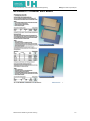
1
BACHELOR OF ENGINEERING DEGREE WITH HONOURS IN
DIGITAL SYSTEMS AND COMPUTER ENGINEERING
Final Year Project Report
School of Electronic, Communication and Electrical Engineering
University of Hertfordshire
Radio Tag for Item Tracking
Report by
Ramiz Ahmed
Supervisor
Dr. Mohammed Jamro
Date
May 2009
DECLARATION STATEMENT
I certify that the work submitted is my own and that any material derived or quoted from the
published or unpublished work of other persons has been duly acknowledged (ref. UPR
AS/C/6.1, Appendix I, Section 2 – Section on cheating and plagiarism)
Student Full Name: Ramiz Ahmed
Student Registration Number: 05102934
Signed: …………………………………………………
Date: 20 April 2009
School of Electronic, Communication and Electrical Engineering
BEng Final Year Project Report
ABSTRACT
This report details the designing, building and testing stages of a Radio Tag Tracking System
which was undertaken as a final year project by the author of this report.
The project consisted of the development of the above said system components, namely the
Radio Tag and a Base Station. Each of the components had to be developed according to a
specified criterion involving size, weight, operation and communication methods. The design
and development stages of each of the components have been discussed separately in this
report.
During the project, an active Radio Tag was designed and developed using PIC
Microcontrollers and low cost AM Transmitters. Each of the component circuits were carefully
designed and tested and has been discussed in detail in relevant chapters of this report.
The Base Station was constructed to keep track of the radio tags by detecting RF signals
transmitted by the Radio Tags. All the hardware and software design, development and testing
stages have been discussed in detail in relevant chapters of this report.
Ramiz Ahmed / Radio Tag for Item Tracking
i
School of Electronic, Communication and Electrical Engineering
BEng Final Year Project Report
ACKNOWLEDGEMENTS
I would like begin with thanking God Almighty for giving me strength and knowledge to finish
this project. I would also like to wish my sincere gratitude to Dr. Mohammed Jamro for
supervising the project and providing guidance to smooth the project work.
I would also like to thank Dr. David Lauder for answering my endless questions and correcting
silly mistakes. Special thanks to Mr. John Wilmot and Mr. Ian Munro for dealing with my endless
requests in the lab work.
Finally I would like to thank my family especially my mother for their continuous support and
blessings during all my time in university.
Ramiz Ahmed / Radio Tag for Item Tracking
ii
School of Electronic, Communication and Electrical Engineering
BEng Final Year Project Report
TABLE OF CONTENTS
DECLARATION STATEMENT ........................................................................................................i
ABSTRACT .....................................................................................................................................i
ACKNOWLEDGEMENTS .............................................................................................................. ii
TABLE OF CONTENTS ................................................................................................................ iii
LIST OF FIGURES .........................................................................................................................v
GLOSSARY .................................................................................................................................. vii
1.
2.
INTRODUCTION .................................................................................................................. 1
1.1
Project Description ........................................................................................................ 1
1.2
Project Objectives ......................................................................................................... 1
1.3
Report Outline ............................................................................................................... 2
PROJCECT PLAN AND WORK STAGES ........................................................................... 3
2.1
3.
2.1.1
RFID Tags ............................................................................................................. 3
2.1.2
Radio Frequency Bandwidth Selection ................................................................. 4
2.2
Hardware Selection ....................................................................................................... 5
2.3
Hardware Design and Assembly ................................................................................... 5
2.4
Testing ........................................................................................................................... 6
Radio Tag (RF Transmitter) .................................................................................................. 7
3.1
Hardware Selection ....................................................................................................... 7
3.1.1
PIC 16F88 Microcontroller ..................................................................................... 8
3.1.2
EasyPIC4 Development Board.............................................................................. 9
3.1.3
Micro TX Transmitter Module .............................................................................. 10
3.2
Circuit Design and Assembly ...................................................................................... 11
3.2.1
MCU circuit Design and Assembly ...................................................................... 12
3.2.2
Micro Tx Transmitter circuit Design and Assembly ............................................. 16
3.2.3
Complete Tag Assembly ..................................................................................... 18
3.3
Microcontroller Software Code .................................................................................... 18
3.3.1
MikroC Compiler & Software ............................................................................... 18
3.3.2
Initial Software Code ........................................................................................... 19
3.3.3
Final Software Code ............................................................................................ 25
3.4
Testing ......................................................................................................................... 26
3.5.1
Software Testing ................................................................................................. 26
3.5.2
Hardware Testing ................................................................................................ 28
3.5.3
Complete Tag Testing ......................................................................................... 30
3.5
4.
Feasibility Study ............................................................................................................ 3
Summary ..................................................................................................................... 32
Base Station (RF Receiver/Reader) ................................................................................... 33
4.1
Hardware Selection ..................................................................................................... 33
Ramiz Ahmed / Radio Tag for Item Tracking
iii
School of Electronic, Communication and Electrical Engineering
4.1.1
PIC 16F877A ....................................................................................................... 34
4.1.2
AM2000 RX 433 Receiver ................................................................................... 35
4.1.3
EasyPIC4 Development Board............................................................................ 35
4.2
Circuit Design and Assembly ...................................................................................... 36
4.2.1
Power Management ............................................................................................ 36
4.2.2
AM2000 Receiver Circuit Design and Assembly................................................. 36
4.2.3
Complete Base Station Assembly ....................................................................... 37
4.3
Microcontroller Software Code .................................................................................... 38
4.4
Testing ......................................................................................................................... 43
4.4.1
Wired (Serial) Communication Testing ............................................................... 44
4.4.2
Wireless (RF) Communication Testing ............................................................... 45
4.5
5.
BEng Final Year Project Report
Summary ..................................................................................................................... 46
Conclusion .......................................................................................................................... 47
5.1
Project Outline and Achievements .............................................................................. 47
5.1.1
System Hardware Design and Assembly ............................................................ 47
5.2
Project Time Plan and Costing .................................................................................... 48
5.3
Recommendations for Further Work ........................................................................... 49
5.3.1
Radio Tag ............................................................................................................ 49
5.3.2
Base Station ........................................................................................................ 50
REFERENCES ............................................................................................................................ 51
BIBLIOGRAPHY.......................................................................................................................... 53
APPENDIX A Final Project Time Plan ........................................................................................ 54
APPENDIX B Final Component List ............................................................................................ 55
APPENDIX C Relevant Part of UK Frequency Allocation Table for Frequency Use .................. 56
APPENDIX D Relevant Part of UK Frequency Allocation Table for Radiated Power ................. 57
APPENDIX E Relevant Pages from PIC 16F88 Datasheet ........................................................ 58
APPENDIX F Relevant Information from EasyPIC4 Development Board User Manual ............. 61
APPENDIX G Relevant Pages from Micro Tx Transmitter Module Datasheet ........................... 63
APPENDIX H Radio Tag Circuit Schematic ................................................................................ 65
APPENDIX I Radio Tag Software Code & Data Flow Diagram .................................................. 66
APPENDIX J Radio Tag Testing Results .................................................................................... 67
APPENDIX K Base Station Software Code and Data Flow Chart .............................................. 68
APPENDIX L Colander Vero Board ............................................................................................ 71
APPENDIX M Relevant Pages from PIC 16F877A Datasheet ................................................... 72
APPENDIX N Relevant Pages from AM2000 RX 433 Receiver Module .................................... 74
APPENDIX O Email Correspondence with LPRS about AM2000 Receiver Module .................. 76
Ramiz Ahmed / Radio Tag for Item Tracking
iv
School of Electronic, Communication and Electrical Engineering
BEng Final Year Project Report
LIST OF FIGURES
Figure 1-1 Conceptual System Block Diagram ............................................................................. 2
Figure 3-1 Block Diagram of the Radio Tag .................................................................................. 7
Figure 3-2 PIC 16F88 Pin Diagram
[7]
........................................................................................... 8
Figure 3-3 Diagram for EasyPIC4 Development Board explaining key components
[8]
................ 9
Figure 3-4 Complete Radio Tag Hardware ................................................................................. 11
Figure 3-5 Decoupling a PIC 16F88 MCU .................................................................................. 13
Figure 3-6 Radio Tag Block Diagram .......................................................................................... 13
Figure 3-7 Pin Map for the Tag No using 8 Pin DIP Switch ........................................................ 13
Figure 3-8 A Typical SIL Network Resistor
[15]
............................................................................ 14
Figure 3-9 Prototype MCU circuit with DIP switch and PIC 16F88 ............................................. 14
Figure 3-10 Final PIC MCU Circuit on Vero Board ..................................................................... 15
Figure 3-11 Application circuit diagram for Micro Tx Module
[5]
.................................................. 16
Figure 3-12 Complete Circuit for the Micro TX Transmitter Module ........................................... 18
Figure 3-13 Initial Radio Tag Software Code Version 2 (1 of 3) ................................................. 20
Figure 3-14 Initial Radio Tag Software Code Version 2 (2 of 3) ................................................. 21
Figure 3-15 Initial Radio Tag Software Code Version 2 (3 of 3) ................................................. 24
Figure 3-18 Memory Usage Statistics for Initial Software Code Version 2 ................................. 25
Figure 3-17 USART Terminal Window with Tag Serial# Being Transmitted .............................. 27
Figure 3-18 Oscillator Output Waveform @ 8 MHz .................................................................... 28
Figure 3-19 MCU Tx Pin Output Waveform @ Serial # 15 ......................................................... 29
Figure 3-20 Frequency Spectrum for Micro Tx Transmitter @ 433 MHz .................................... 30
Figure 3-21 Frequency Spectrum for Complete Tag with serial # 63 ......................................... 30
Figure 3-22 Output of the Radio Software @ Tag Serial # 63 .................................................... 31
Figure 4-1 Conceptual Block Diagram of Base Station (Reader) ............................................... 33
Figure 4-2 PIC 16F877A Pin Diagram
[20]
.................................................................................... 34
Figure 4-3 Picture of an AM2000 RX 433 Receiver
Figure 4-4 AM2000 RX433 Receiver Pin Diagram
[22]
[22]
............................................................... 35
................................................................ 37
Figure 4-5 Complete Base Station .............................................................................................. 38
Figure 4-6 Base Station Software Code Section 1 ..................................................................... 39
Figure 4-7 Base Station Software Code Function Definition Section ......................................... 42
Figure 4-8 Wired Communication Testing Setup with Radio Tag & Base Station ...................... 44
Ramiz Ahmed / Radio Tag for Item Tracking
v
School of Electronic, Communication and Electrical Engineering
BEng Final Year Project Report
Figure 4-9 Complete Base Station .............................................................................................. 44
Figure 4-10 Wireless Comm. testing setup with Tag & Base Station Separate.......................... 45
Ramiz Ahmed / Radio Tag for Item Tracking
vi
School of Electronic, Communication and Electrical Engineering
BEng Final Year Project Report
GLOSSARY
AM
Amplitude Modulation
I/O
Input/Output
MCU
Microcontroller Unit
Ofcom
Office of Communication
RF
Radio Frequency
RFID
Radio Frequency Identification
Rx
Receiver
Tx
Transmitter
Ramiz Ahmed / Radio Tag for Item Tracking
vii
School of Electronic, Communication and Electrical Engineering
BEng Final Year Project Report
1. INTRODUCTION
This report details the steps taken and the methodologies adopted in order to achieve the
aims and objectives for the project. This document is intended to be read by electronic
engineers or technologists and contains complete details of project research, design and
testing of Radio Tags for Item Tracking.
1.1
Project Description
Radio Frequency Identification (RFID) is no longer an emerging technology in today‟s world.
Billions of tags are manufactured and used every year around the world. These tags not only
just provide an alternative to traditional barcodes as form of automatic identification, but they
are also an efficient way to reduce human intervention and space required to identify, track
and trace items. The most common implementation of the technology is by using a RFID Tag
and a RFID reader, the two components interact with each other using Radio Frequency (RF)
in order to store and remotely retrieve data
[1] [2]
.
The key aim of this project was to develop a system to detect when an item is removed from
the area where it should be kept. The system should be suitable for items such as furniture
that need to be moveable within their normal area of use and cannot easily be fitted with a
security cable. It could also be used for computers, whether desktop or portable. Unlike
security tags used in shops this system was not to require a barrier or arch to detect when
tags are moved out of the permitted area
1.2
[1]
.
Project Objectives
In order to progress towards the aims of this project, certain objectives were highlighted and
carefully planned tasks were devised. Further detailed specifications for the tracking system
were then highlighted in the following points
[1] [2]
:-
Design and development of a low cost, compact and battery operated Tag
System should have a base station that can receive signals from up to 256 tags
The distance should be adjustable in the range 1 – 20 metres.
The alarm should include a siren and a programmable voice announcement
There should be two types of tags, a simple transmit only tag and a more advanced
transmit/receive tag.
There should be a portable receiver that can be used to locate tags that have been
removed from the permitted area by searching for the radio signals from the tag.
In the case of a transmit/receive tag, there should be an option to send a command to
the tag to emit a „beeping‟ sound.
Ramiz Ahmed / Radio Tag for Item Tracking
1
School of Electronic, Communication and Electrical Engineering
BEng Final Year Project Report
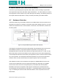
Figure 1-1 Below Illustrates a conceptual block diagram of the Tracking System that was
envisaged during the feasibility study stage of the project plan. The feasibility study is
discussed in detail in the second chapter of this report
Figure 1-1 Conceptual System Block Diagram
1.3
Report Outline
The main focus of this report is to facilitate the reader with all the details of the project
research, design, testing and implementation in the development of the Tag Tracking system.
The different chapters in this report discuss the following project stages:
Chapter 2 provides a brief overview of the initial feasibility study on the research
topic, the project stages and project time plan. The initial literature and hardware
research done in accordance with the project time plan is also discussed in the later
sub-sections of this chapter.
Chapter 3 covers a detailed description of the project management aspects of the
Radio Transmitter Tag part of the tracking system. It details the hardware design,
hardware assembly, software design and testing of the Tag.
Chapter 4 details the second part of the tracking system and details hardware and
software design of the Rx (Base Station) part of the Tracking System.
Chapter 5 provides a detailed discussion of the achieved results, modified project
time plan and component costing, as well as recommendations for further work in the
project area.
Ramiz Ahmed / Radio Tag for Item Tracking
2
School of Electronic, Communication and Electrical Engineering
BEng Final Year Project Report
2. PROJCECT PLAN AND WORK STAGES
This chapter provides a brief overview of the initial research carried out on the project topic
and discusses the key elements that were essential to achievement of project aims and
objectives.
2.1
Feasibility Study
T he initial stages of the project required a detailed feasibility study of the project objectives,
in order to highlight important aspects in the previous research in the related project field and
challenges that could be anticipated in the initial phases of the project. The feasibility study
also included development of a project time plan, providing an approximate time plan and
work stages within the project. A copy of the final project time plans has been added in
Appendix A.
Since the project was part of the development on a research project started in the previous
year much of the initial research had been done by the previous year student. This included
research on the RF frequency to be used and the choice of the RF components, however,
none of the components, except a development board, used in the previous year were
available, the project report had insufficient detail, misleading circuit schematics and the
software code was insufficient for the operation of the whole tracking system. It was therefore
chosen to start the project from scratch by doing the research on the RF frequency to be used
and evaluation of the components used in the previous year.
2.1.1 RFID Tags
The most common implementation of RFID Technology is in RFID Tags, used for tracking
and/or identifying objects, whether material or human. The Radio Frequency (RF) Tags
usually consist of at least two essential parts, an integrated circuit to store and process
information, RF modulation/demodulation etc. And an antenna for receiving and transmitting
the radio signals. According to the number of components, the Radio Tags could then be
classified as:-
Read Only: The data stored on the tag could only be read, if the tag is within the range of the
reader and cannot be edited in anyway.
Read/Write Tags: The data on these tags can be edited, added to, or completely rewritten
but again only if the tag is within the range of the reader.
Ramiz Ahmed / Radio Tag for Item Tracking
3
School of Electronic, Communication and Electrical Engineering
BEng Final Year Project Report
The Tags are then further classified in the types depending on the type of power circuitry.
These types include
[2]
:-
Active Tags: These contain a battery that powers the microchip and allows the tag to
transmit periodic signals to the reader.
Passive Tags: These kinds rely solely on the power generated by the electromagnetic
waves transmitted by the reader; the waves are absorbed by the antenna within the
tag to generate current for microchip to start transmitting information. This means
these tags have to be within the range of the Reader for detection, which would
generally be a barrier or Arch.
Semi-Active (or semi-passive) Tags: These contain a battery to run the circuitry of the
chip, but need to draw power from electromagnetic waves in order to communicate
with the reader.
The addition of battery in active tags makes them considerably expensive compared to
passive tags. Their overall life time is also reduced since battery‟s have only finite amount of
electricity in them. However, Active Tags have better application potential since they do not
require any barrier or arch to detect them. It was after this initial research, it was decided to
use Active Tag circuit methodology for the Radio Tags in the project. The active tags allow
flexibility in design aesthetics like cost, design, size and weight (as they do not specifically
need to be miniature in size).
2.1.2 Radio Frequency Bandwidth Selection
The allocation of radio spectrum in UK is regulated by the standardization organisation
“Ofcom”. The body defines and monitors the allocation of radio frequency bandwidths and
classifies them in different applications like radio and TV broadcasting, for telecommunication
operators, for defence forces, and for civilian use. Generally in order to use a classified radio
frequency band, a formal permission from the governing bodies is a pre-requisite. The
standardization of telecommunication equipment and network in Europe is controlled by
European Telecommunication Standards Institute (ETSI)
[4]
.
Office of Communication (Ofcom) mainly controls the standardization of RF spectrum within
UK, it overlooks industries like telecommunications, broadcasting, intelligent transportation,
professional and amateur radio broadcasting and etc.
Ofcom has allocated some frequency bands in the UK RF Spectrum with licence exempt
classification (without licence approval). The band allocations have carefully been allocated
and listen in the official RF Spectrum Allocation Table
[4]
, and extract from the Issue 15 of the
allocation table has been added into Appendix C. It was after carefully consulting this
Ramiz Ahmed / Radio Tag for Item Tracking
4
School of Electronic, Communication and Electrical Engineering
BEng Final Year Project Report
allocation table, the Radio Frequency of 433 MHz was chosen as the suitable frequency for
communication for this project. The frequency band (432 – 438) is licence exempt and the
frequencies in the lower end of the band have maximum radiated power of only 1 mW. The
frequency was deemed suitable for application in this project because of ready availability of
type approved components from manufacturers within the UK and low power radiation meant
less battery usage and limited range communication.
2.2
Hardware Selection
The feasibility study also included the initial costing for the project, detailing the components
that could be required to complete the project and costs for each of the components. A table
detailing costs of the main components used during the project is included later in this
section. A detailed component list has been added in Appendix B.
2.3
Hardware Design and Assembly
The hardware design and assembly was also divided into two stages. The first stage involved
design and assembly of the Radio Tag part and the second stage involved design and
assembly of the Base Station interface of the project. The selection of hardware components
was based on a range factors which were essential to project aims and objectives and time
plan. The selection depended on:
Radio Frequency Licensing – The RF frequency being used should be license
exempt in UK and/or EU and the components operating at those frequencies should
also be certified (by OFCOM) and have low transmission power.
Size – Since the tags were to be used on movable items, the size of the tag was to be
kept minimal with as little components as possible
Power Consumption – The power consumption of the components was to be kept
significantly low in order for tags to be operated using a standard battery over a
longer period of time.
Cost – The cost was to be a major factor in the design of the tracking system.
Although active tags are expensive than conventional passive tags, the actual cost of
the components was to be kept to be a minimum to relate the project to its potential
market value.
The maximum budget allowed for the project by the School of Electronic, Communication and
Electrical Engineering was £50, while most of the RF components had higher costs and the
development board being used for the receiver side alone was approximately £80. However,
the costing problem was solved by using the EasyPIC4 development board used in the
previous year project. This allowed the budget money to be used to purchase the
RF transmitters and receiver components from specialist manufacturers. The microcontrollers
Ramiz Ahmed / Radio Tag for Item Tracking
5
School of Electronic, Communication and Electrical Engineering
BEng Final Year Project Report
and other smaller components were sourced from within the university stores which helped in
keeping the prototype development costs to minimum. A concise cost list has already been
listed in section 2.2.
Post hardware design stage, the hardware assembly was carried out whilst adhering to
professional circuit assembly practices and the hardware size and weight criterion.
2.4
Testing
Once the hardware design and assembly phases were successfully complete, the system
was tested to ensure its performance was according to the expected criteria. The testing was
done using different analysis criteria and instruments. The testing was done in conditions
similar to normal operational conditions of the tags with high level of noise and distance
losses.
The results were then analysed to confirm the overall system performance and chalk out any
hardware and software errors.
Ramiz Ahmed / Radio Tag for Item Tracking
6
School of Electronic, Communication and Electrical Engineering
BEng Final Year Project Report
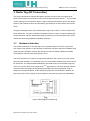
3. Radio Tag (RF Transmitter)
The project specifications required the battery operated Tag to be able to transmit an RF
beacon after specific time intervals in order to be tracked by the base station
[1]
. This provided
certain challenges in the interface design of tag‟s hardware and software. Both of the design
aspects, with possible solutions and final design specifications are discussed in the sections
below.
During the feasibility study it was decided that the tag would consist of a microcontroller and
an RF transmitter. The microcontroller would perform all the number crunching regarding tag
number detection and then would transmit the tag number to an RF transmitter which would
transmit the data using amplitude modulation technique.
3.1
Hardware Selection
The hardware selection for the radio tag was an important stage in the whole project time
plan. Much of the research on the hardware components was done during the feasibility study
stage and further literature research was carried out whilst considering different hardware
characteristics and final component selection done.
The microcontroller to be used for the tag number detection was chosen to be a PIC 16F88
microcontroller and Micro Tx Transmitter from Low Power Radio Solutions was chosen as the
RF transmitter. The AM (Amplitude Modulation) transmitter works at 433.92 MHz Frequency
which is low power and licence exempt in UK
[4] [5]
[Appendix C]. The microcontroller software
code was written using MikroC programming language and it was programmed using an
EasyPIC4 Development Board. All the hardware components are described in detail in the
later sub-sections of this chapter. A block diagram of the Radio Tag has been added below.
Figure 3-1 Block Diagram of the Radio Tag
Ramiz Ahmed / Radio Tag for Item Tracking
7
School of Electronic, Communication and Electrical Engineering
BEng Final Year Project Report
3.1.1 PIC 16F88 Microcontroller
PIC 16F88 is an 18-pin, 16 Bit MCU (Micro-Controller Unit) from the Mid-Range family of the
PICmicro® devices by Microchip
[7]
. The microcontroller was chosen as the control logic for
the tag circuit because of its low cost, compact size, free development tools, and serial
programming/re-programming with flash memory capabilities. The microcontroller also has
some special features which were particularly useful considering the scope of the project. A
pin diagram of the PIC 16F88 has been included below (also see Appendix E for relevant
MCU information). The special features included
[6] [7]
:-
100,000 erase/write cycles in flash program memory
EEPROM Data Retention:> 40 years
In- Circuit Serial Programming™ (ICSP™) via two pins
Extended Watchdog Timer (WDT)
Wide operating voltage range: (2.0V to 5.5V)
Low power consumption
Variety of Oscillator Modes with 8 user selectable frequencies ( 31 KHz – 8 MHz)
Addressable Universal Synchronous Asynchronous Receiver Transmitter
(AUSART/SCI) with 9-bit address detection.
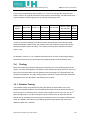
Table 1 PIC 16F88 Specifications
Parameter Name
Value
Program Memory type
Flash
Program Memory(KB)
4 x14
CPU Speed (MIPS)
5
RAM Bytes
368 x 8
Data EEPROM (bytes)
256 x 8
Timers
2 x 18-bit, 1 x 16-bit
ADC
7 ch, 10-bit
Comparators
2
Serial Comms
USART
I/O Ports
Ports A, B
Instruction Set
35 Instructions
Resets
POR, BOR
Temperature Range (C)
-40 to 125
Operating Voltage
Range (V)
Pin Count
PIN Diagram
Figure 3-2 PIC 16F88 Pin Diagram
[7]
2 to 5.5
18
Ramiz Ahmed / Radio Tag for Item Tracking
8
School of Electronic, Communication and Electrical Engineering
BEng Final Year Project Report
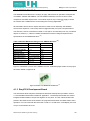
3.1.2 EasyPIC4 Development Board
The EasyPIC4 development system is a development board for PIC Microcontrollers. It is
designed to allow students and engineers easily explore and test the capabilities of PIC
microcontrollers. The development board can be used to interface PIC microcontrollers with
external circuits and a broad range of peripheral devices, allowing a user to concentrate on
software development
[8] [9]
.
Each of the components on the board is marked on the silk screen on both top and bottom
sides of the board, describing connections to microcontrollers and operational modes. Since
all the relevant information is printed on the board, the board is very easy to use and no
additional schematics are required. Figure 3-3 illustrates the development board with its
important components explained
[8, 9
.
The board can easily be connected to the USB port of a computer with an installed version of
MikroC programming language using a USB 2.0 cable. User can insert a PIC microcontroller
into its relevant socket and then program it through the USB connection using the PICFlash2
Programming software supplied with the development board
[8] [9]
.
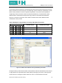
Figure 3-3 Diagram for EasyPIC4 Development Board explaining key components
Ramiz Ahmed / Radio Tag for Item Tracking
[8]
9
School of Electronic, Communication and Electrical Engineering
BEng Final Year Project Report
The EasyPIC4 development board features a number of peripheral devices and therefore in
order to enable these devices before programming any PIC microcontroller, it is important to
check if appropriate jumpers or switches have been properly set
[8] [9]
. Although the board has
numerous components and peripheral devices, components relative to this project have only
been explained in Appendix F. For further information about board operation, the user manual
for EasyPIC4 development board should be consulted
[8]
.
3.1.3 Micro TX Transmitter Module
Micro TX is a low cost, type approved, RF transmitter which works at UHF (Ultra High
Frequency), manufactured by Low Power Radio Solutions. The module is compatible with low
cost super-regenerative and AM superhet receivers. The datasheet for the module was
consulted before purchasing the module to ensure it‟s electrical and hardware specifications
were in accordance with the project aims.
The module has a sub-miniature two-pin package which makes it very useful to be applied in
circuits where space is limited and the overall circuit design is compact
[5]
. Since one of the
aims of the projects was to create a radio tag which is compact in size, the Micro TX module
passed the selection criteria.
The unique design of the module allows it to be operated on any supply voltage between 2.5
and 13V, simply by changing one external resistor and it is compatible with most encoding
ICs operating from 3V to 12V
[5]
. The transmit pin on PIC 16F88 microcontroller works at 5V
DC which ensured the electrical specifications of the module were compatible with the
microcontroller.
The module works at 433.845 MHz frequency and can achieve up to -6 dBm radiated power
with a 90mm whip antenna, however, its best operational performance could be achieved by
using a standard ¼ wave whip antenna. The antenna used with the module was therefore
chosen as a ¼ wave whip antenna
[16]
to allow for best operational performance.
The datasheet for the module also stated that it has an operational range of up to 100
metres
[5]
. That ticked another of the selection criteria of tag range to be from 1 – 20 metres.
Table 2 details the detailed technical specifications of the module.
Ramiz Ahmed / Radio Tag for Item Tracking
10
School of Electronic, Communication and Electrical Engineering
Table 2 Micro Tx 433 Transmitter Absolute Maximum Ratings
BEng Final Year Project Report
[5]
Parameter
Typical
Units
Frequency (UK)
433.92
MHz
Module Voltage
2.2 – 3.0
Volts
Input Current (mark)
3.0 – 4.6
mA
Input Current (space)
0
mA
Effective Radiated Power (ERP)
-6
dBm
Maximum Baud rate
1200
bps
Range (with suitable receiver)
100
Metres
Dimensions
8.5 x 7.0 x 4.2 +/- 10%
mm
Pin Pitch
5.08
mm
Operating Temperature
-10 - +40
deg. C
Storage Temperature
-40 - +85
deg. C
Matching Receiver
AM2000 Receiver
N/A
Supply voltage (RD = 680 Ohms)
Relevant pages from the module‟s datasheet have been added into Appendix G. During
circuit design, multiple changes were applied to the application circuits recommended in the
datasheet. The changes have been discussed in later sub-sections of this chapter.
3.2
Circuit Design and Assembly
The circuit design stage for the Radio Tag was completed after detailed project research and
by consulting the data sheets for the PIC microcontroller and the Micro Tx module. A number
of reference books and internet sources were consulted to identify the right components for
the microcontroller circuit and follow the manufacturer‟s guidelines. The hardware design and
assembly was done to the best possible professional approach and all special care was taken
to reduce costs and create an efficient hardware prototype.
Figure 3.4 below shows the final hardware circuit, the main schematic for the Radio Tag
hardware is also given in Appendix H. The important components in the hardware have been
labelled in the diagram below.
Figure 3-4 Complete Radio Tag Hardware
Ramiz Ahmed / Radio Tag for Item Tracking
11
School of Electronic, Communication and Electrical Engineering
BEng Final Year Project Report
In order to avoid mistakes in final circuit and allow for modular testing, the circuit assembly
was divided into two stages.
Microcontroller (MCU) circuit assembly
Micro Tx circuit assembly
Details of the circuit assembly stages have been discussed in the later sub-sections of this
chapter.
3.2.1 MCU circuit Design and Assembly
The first step in power management of the circuit was to check the voltage and current usage
of all the components in the circuit. The table below details the power budget for the Radio
Tag circuit.
The microcontroller voltage and current consumption values were obtained from the relevant
datasheets given in Appendix E. The microcontroller works with 5V DC supply and any of its
input/output (I/O) ports can source or sink up to 25mA current. Therefore pin 14 (VDD) pin of
the microcontroller was connected to the 5V DC power supply rail. As all the electronic
devices need a ground connection to work, pin 5 (VSS) of the microcontroller was connected
to ground (0V) rail. The ground rail was made a common ground between all the components
on the circuit board.
The microcontroller has a MCLR pin (pin 4, RA5/MCLR/VPP), which could be used to RESET
the microcontroller so that it should start executing its program code from the beginning.
Since, the project aims and objectives did not require the Tag to be reset at any time in
operation; no Reset button was added to the tag circuit. However, the MCLR pin needs to be
pulled up to the VDD (5V) in order to allow the microcontroller to start working. But voltage
spikes at the MCLR pin can cause the processor to latch-up, so rather than tying the pin
directly to VDD, a series resistor of value 10 kilo-ohm was used to pull MCLR to VDD
[6]
.
One important step during the power supply management of the circuit was to ensure
decoupling of the power supply rails. Most power supplies, sometimes supply an AC signal
superimposed on the DC power line, such noise signals are mostly undesirable in powered
circuits
[10] [11]
and in RF systems, these noise signals can easily result in unwanted
oscillations. A common RF decoupling technique is to feed the DC supply to each stage
through a path that has high impedance at signal frequencies but low impedance at DC
[12] [13]
.
During transition of the circuits from one state to another (and from low current requirements
to high), the internal (and external) current draws inside the chip change, which produce
fluctuations in the internal voltage levels of the microcontroller chip, causing it to lock up, reset
Ramiz Ahmed / Radio Tag for Item Tracking
12
School of Electronic, Communication and Electrical Engineering
BEng Final Year Project Report
or behave unpredictably in other ways. The decoupling capacitor filters the power fluctuations
and provides a stable power supply for the chip
[14]
. Therefore, a 100uF electrolytic capacitor
was connected between the all the VDD pins and wired to ground, as shown in Fig 3-5 below.
Figure 3-5 Decoupling a PIC 16F88 MCU
The circuit design involved connecting an 8 pin DIP switch (see figure 3-6 below) to the
microcontroller. As described in Section 2.1 the DIP switch is used to input the Tag serial
number into the microcontroller.
Figure 3-6 Radio Tag Block Diagram
Since the microcontroller would read the DIP switches as individual binary numbers, the 8
8
Switches could provide us with a possible 2 – 1 = 255 different tag numbers. A pin map of
the DIP switch with the microcontroller ports and their equivalent decimal value is given in
figure 3-7 below.
Figure 3-7 Pin Map for the Tag No using 8 Pin DIP Switch
The DIP switch is connected to RA0, RA1, RA2, RA3 and RB0, RB1, RB2, RB3 pins of the
microcontroller. The input of the DIP switch is connected in parallel to the 5V Power Supply to
the microcontroller, providing 5V to each of the switches. If any of the 8 switches is turned to
Ramiz Ahmed / Radio Tag for Item Tracking
13
School of Electronic, Communication and Electrical Engineering
BEng Final Year Project Report
ON position then the 5V volts are applied to the corresponding pin of the microcontroller. The
above stated pins on the microcontroller were declared as inputs in the microcontroller‟s
program code, which allowed the tag serial number to be read in to the program (see section
3.5.1 for examples of Tag serial numbers). If any of the switches were turned off in any
particular tag serial number, the MCU pins connected to these switches would be left floating.
This has an undesirable effect of stray micro-volts being fed into the MCU pins and a wrong
resultant tag number being read into the MCU. In order to eliminate this effect a 4.7 kilo-ohm
pull-down resistor was connected to each of the microcontroller pins and ground (0V).
Connection of the resistor with MCU means if any of the DIP switches are off then the
corresponding MCU pin is pulled down to ground and a constant 0V is read at that pin.
Adding individual resistors to the pins meant extra wiring connections from the microcontroller
to the ground. To avoid cluttering the circuit board with multiple resistors, an 8 pin 4K7
network resistor
[15]
was used.
Figure 3-8 A Typical SIL Network Resistor
[15]
The network resistor assists in reducing the number of components and soldering pins in the
circuit. The 8 pins were therefore connected in parallel with MCU‟s Pins and the common pin
was connected to the ground (0V) connection.
All microcontrollers need a clock signal to work with. The PIC 16F88 microcontroller has
internal oscillator but for better performance an external oscillator could be used with the
microcontroller. To achieve better and accurate performance, an external 8 MHz crystal
oscillator was connected to the RA7/OSC1 and RA6/OSC2 pins of the microcontroller. As
stated in the product datasheet, two 22 pF capacitors were connected between the oscillator
pins (one each on each pin of the oscillator) and the Ground (0V) to allow for a basic start-up
time and stable oscillator operation
[6]
.
The MCU circuit was first assembled on a prototyping breadboard. The prototype was then
used to test the overall operation and stability of circuit design including the DIP switch and
the oscillator operation. A picture of the prototype MCU circuit is added below in Figure 3-9.
Figure 3-9 Prototype MCU circuit with DIP switch and PIC 16F88
Ramiz Ahmed / Radio Tag for Item Tracking
14
School of Electronic, Communication and Electrical Engineering
BEng Final Year Project Report
Once satisfied, the microcontroller circuit was then transferred over to a Vero board
(Appendix L). All of the circuit components were through-hole components and therefore no
problem was encountered in placing any of the components on to the board. An 18 pin DIP
socket was soldered in place of the microcontroller, and the microcontroller was then placed
in the socket. This was done to assist in the programming phase of the project, where
microcontroller could easily be taken out of its socket and re-programmed with a new version
of program/software code. The components were carefully placed on to the board and their
connection tracks were checked before soldering all of the components to the Vero board. All
the tracks between the adjacent DIP switch pins and DIP socket pins were carefully cut using
a track cutter. This was done to avoid any short circuit between the sensitive components
especially the microcontroller and the oscillator.
After the soldering stage, all the connections were checked under a 7x microscope to check
for any dry joints or bridged connections. A multi meter was then used to check for any short
circuits. Any resulting errors were corrected and soldering was completed and given a
thorough check again before powering up the MCU circuit for the first time.
Since the circuit was built to work as a prototype, standard 5V power supplies in the labs were
used to power up the circuit, this avoided adding extra battery component costs to the overall
project budget. Two wires (red for +5V and black for 0V GND) were soldered onto the power
supply rails on the Vero Board which were then connected to the laboratory power supply to
power up the circuit.
During the hardware testing stages, an LED was connected in series with the data output pin
(RB5, pin 11) of the microcontroller. Since the I/O ports of the MCU can only source up to
25 mA current and the Micro Tx transmitter module draws 4mA current, a 330 ohm resistor
was also added in series between the LED and the MCU pin to limit the current being drawn
by the LED. The LED was added to indicate if the MCU is powered up and is transmitting any
data to the RF transmitter. The final MCU hardware circuit is shown in Figure 3-10 below.
Figure 3-10 Final PIC MCU Circuit on Vero Board
Ramiz Ahmed / Radio Tag for Item Tracking
15
School of Electronic, Communication and Electrical Engineering
BEng Final Year Project Report
3.2.2 Micro Tx Transmitter circuit Design and Assembly
The main task in designing the Micro Tx transmitter circuit was identifying the right application
circuit in its datasheet (Appendix G) and then identifying the right components according to
the MCU circuit specifications. The right application circuit diagram from the relevant data
sheet
[5]
is given in the Figure 3.11 below.
Figure 3-11 Application circuit diagram for Micro Tx Module
[5]
As explained earlier in section 3.1.3, the Tx pin (RB5) of the PIC 16F88 MCU provides a 5V
supply voltage when its transmitting data and the Micro TX module could work on any voltage
between 2.5 V and 13V. The resistor value table provided in the datasheet was used to
identify the value of the series Rd shown in the circuit diagram above. The voltage range was
chosen as 4.2V to 6.1V and hence the Rd value is 680 ohm. The recommended value of RF
choke in the data sheet is 100 uH. The complete schematic of the Radio Tag including the
Micro TX transmitter circuit has been added in Appendix H.
Table 3 Bill of Materials for Micro Tx Transmitter Circuit
Item #
Description
Quantity
1
Resistor, 680 Ohm
1
2
RF Choke, 100 uH
1
3
Capacitor 220 pF
1
4
Inductor, 15 nH
1
5
Variable Capacitor, 2 – 5 pF
1
6
¼ Wave Whip Antenna
1
An important aspect to note is identifying the polarity of the transmitter module. The package
dimension diagram in the datasheet shows that there is a small hole or circle on the +ve pin.
In actual, although there is a small circle visible just above one of the pins of the module, the
actual +ve pin is marked with a red line on that side of the module.
Ramiz Ahmed / Radio Tag for Item Tracking
16
School of Electronic, Communication and Electrical Engineering
BEng Final Year Project Report
The antenna used with the module is a ¼ wave whip antenna which was recommended in the
product datasheet for best performance. The whip antenna is a monopole antenna, with a
single driven element and a ground plane. The antenna is stiff but flexible wire mounted, and
their length determines their wavelength, although it could be shortened with a loading coil
anywhere along the antenna. Whips are generally a fraction of their actual operating
wavelength, with half-wave and quarter wave whips being more common
[16]
. They are
particularly useful in situations where flexibility is an important issue and the antenna
shouldn‟t break when struck. The characteristics of antenna were also feasible for the
application criteria of the radio tags.
In order to achieve low impedance return path for power and signals at all frequencies in RF
system, an effective ground plane is always required. In ideal RF systems, all pointes
connected to the ground must be at the same potential, but in active RF systems, it is not
deemed an easy task due to presence of high frequencies. Common PCB‟s have effective
inductance at their ground tracks. To overcome the effects of inductance problem, a
continuous conductive “ground plane” board can be used.
In a ground plane prototype board, one side is dedicated to running all of the necessary
interconnections between components. The other side is a continuous copper layer and all
ground connections are made to the ground plane. In the case of through-hole mounted
components, a plated-through hole is normally provided whereas for surface-mounted
components or prototype construction, components can be soldered directly to the ground
plane
[12] [13]
. To achieve the best possible performance and reliability in RF system, the
transmitter circuit was assembled on a Colander Vero board. The Vero board is made of
epoxy glass with a colander ground plane for maximum screening (see Appendix L). Since
the circuit is an Ultra High Frequency (UHF) RF system, all the components were soldered as
close to each other as possible to avoid unwanted oscillations and impedance from the circuit
board.
A SMA connector was mounted on top of the circuit board to fix the antenna vertically down
and the connection between the antenna and the inductor (in series with the module) was
established by soldering the connector pin onto the circuit board. The SMA connector legs
were too big in diameter for the through holes on the board, so the holes were enlarged by
drilling through them. The connector legs were then soldered onto the ground plane to ensure
good grounding. A picture of the completed circuit for the Micro TX Transmitter module is
given in the figure below.
Ramiz Ahmed / Radio Tag for Item Tracking
17
School of Electronic, Communication and Electrical Engineering
BEng Final Year Project Report
Figure 3-12 Complete Circuit for the Micro TX Transmitter Module
3.2.3 Complete Tag Assembly
The task of complete tag assembly was completed by connecting the two circuit boards (MCU
circuit board and Micro TX circuit board) together by using electrical wires. One wire was
connected between the Tx pin (RB5) of the microcontroller and the resistor Rd on the module
circuit board. The other wire was used to connect the ground plane on the transmitter circuit
board to the common ground on the MCU circuit board.
A picture of the final Tag Hardware has already been added in Figure 3-4.
3.3
Microcontroller Software Code
The software program for the PIC 16F88 used in Radio Tag was written using mikroC
programming software which is a well known software development tool for PIC
microcontrollers. The compiler has been designed to facilitate users with easiest solutions to
develop embedded applications without compromising performance or control
[18] [19]
.
Different versions of software code were created to ensure effective usage of the speed and
memory space of the microcontroller. The two most noteworthy versions of the software code
including the final version have been discussed in the following subsections.
3.3.1 MikroC Compiler & Software
mikroC has a variety of options that allows its users to quickly create and test complex
applications. The important features include
[18]
Write C code using highly advanced Code Editor
Use the included MikroC libraries to speed up the development, data acquisition,
conversions, displays communications etc.
Ramiz Ahmed / Radio Tag for Item Tracking
18
School of Electronic, Communication and Electrical Engineering
BEng Final Year Project Report
Monitor the program structure, variables, and functions in the Code Explorer.
Generate commented, human-readable assembly, and standard HEX files compatible
with all programmers.
Inspect program flow and debug executable logic with integrated Debugger. Get
detailed reports and graphs on code statistics, assembly listing, and calling tree.
Availability of plenty of examples to expand, develop and use as building bricks in
projects.
One of the other features of the MikroC is its integrated tools. One tool of special interest in
relation to this project is the USART Terminal, the USART (Universal Synchronous
Asynchronous Receiver Transmitter) communication terminal for RS232 communication
[18]
.
The tool was used during the testing stages of the project to verify the output of the
microcontroller used in the Radio Tag. Further information about the MikroC compiler and
development tool could be obtained by referring to its user manual and documentation
[18] [19]
.
Although the University had a full licence of the MikroC software, much of the software code
was developed using the demo version of the software. The demo version has almost all the
operational features of the full version, except the usage of some specialist libraries and the
code length is limited to 1000 lines. The limited usage of libraries resulted in some problems
during the software development which is explained in the later subsections, however, the
code length of 1000 lines was never an issue for this project as much of the code was only
100 or less lines long.
The first step towards writing the software code for the PIC 16F88 microcontroller for radio tag
was to create a basic data flow chart. The aim for developing the flow chart was to show the
flow of information within the micro-controller, modularize the code and makes the code
understandable. The Basic data flow diagram for the Radio Tag part of the system has been
added into Appendix G.
3.3.2 Initial Software Code
The PIC microcontroller provides the feature of reading individual port pins in the software
code (instead of reading the whole 8 pins of the port). Since the 8 pins of the DIP switch were
connected to individual microcontroller pins, the binary values of those pins were read into a
variable array. The main aim in software development was to read in that binary number
correctly into the microcontroller and then transmitted periodically on the USART port (RB5/Tx
Pin). The USART port however transmits data using hexadecimal values. If the array holding
the tag number was to be transmitted using USART the individual elements would have been
Ramiz Ahmed / Radio Tag for Item Tracking
19
School of Electronic, Communication and Electrical Engineering
BEng Final Year Project Report
considered individual numbers and thus a wrong set of values would‟ve been transmitted
through the USART.
One of the possible approaches towards transmitting the tag number correctly was to convert
the individual binary bits in the array to a decimal number and then sending that decimal
number (or its hex value) through USART. But the limitations in the demo version of the
MikroC software didn‟t allow the user of the power() function
[18]
to convert individual binary
numbers to their corresponding decimal number. As a solution to the demo version
limitations, a binary to decimal conversion function along with a binary power converter
function were written within the software code. This slightly increased the memory usage and
function call number in the overall program, but since the overall program execution was very
efficient, addition of these extra functions did not have any noticeable effect on operation of
the microcontroller. The initial software code has been added in the figures below. The code
is distributed into three figures to assist in explanation of the functionality of the code. The
complete software code has been added into Appendix K.
Figure 3-13 Initial Radio Tag Software Code Version 2 (1 of 3)
Figure 3-13above shows the first few lines of the version 2 of the initial software code. Much
of the code is self-explanatory and detailed comments have been used to identify the
functions of each command line. Lines 1-6 are commented lines providing details about the
code file, including the project title, code type, programmers name and version of the software
code.
Lines 10 - 17 declare different global variables being used in the program. The code line:unsigned short TagNo [8];
Ramiz Ahmed / Radio Tag for Item Tracking
20
School of Electronic, Communication and Electrical Engineering
BEng Final Year Project Report
is the declaration of the array TagNo with length of 8 to store the 8 binary numbers being read
into the code. Since the values being read are only binary (either 1 or 0) the data type of the
variable is declared as unsigned short variable array.
Lines 20 and 21 declare the two functions created later in the software to do the binary to
decimal conversion mentioned in the beginning of this section.
Figure 3-14 Initial Radio Tag Software Code Version 2 (2 of 3)
Figure 3.14 above shows the part of the software code where the power and conversion
functions are defined.
Lines 24 to 38 (see figure) form the function where the power function is defined. The function
takes one integer input variable and returns an integer output. The main operation of the
function is to convert the binary number in to its corresponding value. The bits in any binary
0
1
2
3
number ascend in the order of the power of binary numbers e.g. 2 , 2 , 2 , 2 etc. in order to
convert a binary number to decimal number it is important to convert the binary number at
that bit correctly to its decimal value (value of 2 raised to its power, the power is the position
of the bit in the whole binary number).
The first part of the function is a conditional „if‟ statement which checks whether the input
0
given to it is zero or not. If it is zero (i.e. 2 ) then the function returns the value of 1 to its
calling function by default.
Ramiz Ahmed / Radio Tag for Item Tracking
21
School of Electronic, Communication and Electrical Engineering
BEng Final Year Project Report
if (temp2 == 0) {return 1;}
However, if the input value is not integer „0‟ then the „if‟ statement is false and the program
goes to the „else‟ part of the conditional statement. The else part contains a FOR loop which
starts from 1 and terminates at the value input to the function “temp2”.
for (i=1;i<=temp2;i++)
{
Result = Result * 2;
}
return Result;
The loop iterates the code in which it multiplies the value stored in the „Result‟ variable by 2
and then stores the resultant value back to „Result‟ variable. The value is then used in the
next iteration and so on until the loop terminates. After the first iteration, the „Result‟ variable
has value of „2‟ in it. As shown in example below, in the successive iterations this has an
effect of raising the number 2 to its power (the number of iteration in the loop).
Loop 1:
Loop 2:
Loop 3:
Loop 4:
Loop 5:
Result = Result * 2 =
Result = Result * 2 =
Result = Result * 2 =
Result = Result * 2 =
Result = Result * 2 =
1*2
2*2
4*2
8*2
16 * 2
=2
=4
=8
= 16
= 32
≈2
1
≈2
2
≈2
3
≈2
4
≈2
0
After the loop terminates, the value stored in the Result variable is then returned to calling
function.
Lines 42 till 50 form part of the Binary to Decimal conversion b2dec() function. This function
does not take any inputs but returns an integer value stored in its „decimal‟ variable.
for(temp1=0;temp1<8;temp1++)
{
if (TagNo[temp1] ==1)
{decimal = decimal + Power(temp1); }
}
The main part of this function is a FOR loop. The FOR loop starts at zero and terminates at
the value of 7. The reason for the 8 loops is the fact that there are 8 switches connected to
the microcontroller and the array storing the values of those pins is 8 values long. The code in
the loop picks a value from the „TagNo []‟ array (the value corresponds to the loop iteration),
and does a conditional check on the value. If the value in the array is equal to zero (switch at
that pin is OFF i.e. logical zero input), the code skips the rest of the code and goes to the next
loop. However, if the value is 1 (switch at the pin is ON i.e. logical 1 input), then the next line
in the code calls the power() function, the input to the function is the iteration number in the
Ramiz Ahmed / Radio Tag for Item Tracking
22
School of Electronic, Communication and Electrical Engineering
BEng Final Year Project Report
FOR loop. The returned value from the power() function is added to the current value of the
„decimal‟ variable and the resultant value is stored back to the „decimal‟ variable. All of these
operations are done in one code line i.e.
decimal = decimal + Power(temp1);
After termination of the FOR loop, the final value in the „decimal‟ is returned to the calling
function.
The main body of the program starts at line 52. Lines 53 – 60 contain the code which
configures the registers, ports and interrupts in the PIC microcontroller. The following lines
ANSEL = 0x00;
INTCON = 0x00;
Disable the analogue-to-digital converter and interrupts within the PIC MCU as they are not
necessary in the operation of MCU in this particular application. The next lines configure the
pins in PORTA and PORTB as inputs/outputs individually and initialize them at logical value
zero.
PORTA=0x00;
PORTB=0x00;
TRISA = 0b11111111;
TRISB = 0b11011111;
// Initialize Port A at Zero Logic Value
// Initialize Port B at Zero Logic Value
// Declare Port A as Input
// Declare Port B as Input Except RB5 (output)
All the pins in Port A are declared as inputs and all the pins in Port B except port RB5 are
declared as input as well. RB5 in Port B is declared as output since this is the RB5/Tx pin of
the MCU.
Following the port declaration is a FOR loop at lines 63 – 66 (see figure below). The FOR
loop starts at zero and terminates at value 7. The purpose of the FOR loop is to initialize all
the values in the TagNo[] array to zero. This is necessary because otherwise the compiler
would store random values in the array and this could result in unexpected code behaviour or
wrong Tag serial number during program execution. During each iteration, the following line
stores zero at that corresponding value of the array:TagNo[j]=0;
// Assign 0 Value in all values of TagNo Array
Figure 3-15 below illustrates the last part of the version 2 of the initial software code.
Ramiz Ahmed / Radio Tag for Item Tracking
23
School of Electronic, Communication and Electrical Engineering
BEng Final Year Project Report
Figure 3-15 Initial Radio Tag Software Code Version 2 (3 of 3)
The next part of the code (lines 68 – 75) maps the individual pins of Port A and port B to their
corresponding values of TagNo array, and the values are read into the array. A pin map is
already given in Figure 3-7 (Section 3.2.1).
An important aspect in using USART data transmission is to initialize the USART port in the
beginning of the main program body. The USART is initialized at 1200 baud rate, no parity bit,
no stop bits by writing the following command at line 77. The baud rate of 1200 bps is used to
match the data rate with the transmission data rate of the Micro TX Transmitter module (see
section 3.1.3).
USART_init(1200);
// Initialize USART@baud rate of Micro Tx (1200 bps)
Code line 80 is used to store variable delay value in variable „t‟. The variable delay value is
created by adding a modulus “%” of a pseudo random number generated by a library function
“rand()” in the software to the predefined time value which in this case is „dt/2 = 250ms‟. The
rand() function generates a returns a pseudo-random number between 0 – 32767. However,
by taking a modulus of the random by “dt = 500”, the value of the random number is limited to
0 – 500 and therefore the final random time delay is always in between 250ms – 750ms.
Line 81 stores the decimal value of the tag serial number by calling the b2dec() function. The
next line in the code does a conditional check on the decimal value of Tag No. Although in
practical cases there will not be a radio tag with serial number „0‟, this conditional check was
added for exceptional cases and for software testing purposes. If the Tag number is zero the
program goes back into a loop. However if the tag number is greater than zero then the tag
number is transmitter through the USART port using USART_write() command. Following the
Ramiz Ahmed / Radio Tag for Item Tracking
24
School of Electronic, Communication and Electrical Engineering
BEng Final Year Project Report
write command, there is a variable delay in milliseconds before the program goes into another
loop. The variable delay is used as an anti-collision technique to avoid signal collisions when
multiple tags are transmitting to the same base station simultaneously. Much of the anticollision technique is discussed in the „Testing‟ part of this chapter.
The EasyPIC4 board mentioned in 3.1.2 has on-board PICFlash2 Programming software
which was used to program the PIC microcontroller. The microcontroller was placed into its
appropriate 18 way DIP socket and then the board was connected to the computer using a
USB 2.0 cable (provided with the board) and the Build + Program option in the mikroC
software environment was used to generate a HEX file and program the MCU. The memory
usage statistics for the microcontroller are shown in the figure below:-
Figure 3-16 Memory Usage Statistics for Initial Software Code Version 2
Since the all microcontrollers and electronic boards are sensitive to static charge, the board
was placed on an anti-static mat and anti-static bands were used while inserting/removing the
MCU from the board. After programming, the MCU was placed into its circuit socket and the
operation of the code was tested which is explained in „Testing‟ part of this chapter.
3.3.3 Final Software Code
After conducting further research in possible approaches to reading the tag number from DIP
switch the final code version was created. Instead of using an array to read in the tag number
and then converting the binary value to decimal values a simple Bit Masking approach was
applied in the code. This reduced the code length from 92 lines to just 35 lines. The new code
does not require any binary to decimal conversion and there are no function declarations. The
complete source code has been added into Appendix K. The final code has no difference in
the microcontroller configuration and the variable delay. The only difference is the way tag
serial number is read into the system. The command used to read the serial number into the
program memory is
TagNo = (PORTB << 4) | (PORTA & 0x0f);
The variable used to store the tag number is declared as a character data type. In the code
line above the data read in three stages. In the first stage the data read from Port B is
Ramiz Ahmed / Radio Tag for Item Tracking
25
School of Electronic, Communication and Electrical Engineering
BEng Final Year Project Report
arithmetically shifted 4 places to the left. In the second part the data read from Port A is used
to do a logical and with 0x0F (binary 00001111). Then in the last part the result from first
stage is used to do a logical OR with the result from the second stage. The table below gives
a few examples to further highlight the bit masking methodology used.
Actual Tag
Number
Port B input
Port B << 4
Port A input
Port A & 0x0F
(Port B << 4) OR
Tag No
(Port A & 0x0F)
In Hex
2
0000 0000
0000 0000
0000 0010
0000 0010
0000 0010
0x02
15
0000 0000
0000 0000
0000 1111
0000 1111
0000 1111
0x0F
63
0000 0011
0011 0000
0000 1111
0000 1111
0011 1111
0x3F
210
0000 1101
1101 0000
0000 0010
0000 0010
1101 0010
0xD2
In order to avoid the possibility of collision between transmissions of short bursts of data
being transmitted by different tags, the software code was modified to change the random
time delay between 250ms to 750ms. The rand() function has been explained in detail in
section 3.3.2.
As detailed in section 3.5.1, the software was tested for its accuracy using multiple testing
techniques and then the microcontroller was programmed with the final software code.
3.4
Testing
Much of the initial Tag hardware testing was done during the circuit assembly phase of the
project. The same was applied to the software code development phase but some amount of
time in the project time plan was also dedicated to the final testing of combined Radio Tag
hardware and software. The major testing phase of the Radio Tag was therefore divided into
two phases which are described in the following sub-sections.
3.5.1 Software Testing
The software testing was performed by using the RS232 Communication Port on the
EasyPIC4 Development Board. The development board also has push button switches for
each of the pins on the board which could be used to apply 5v DC to any of the port pins
[8]
(also see Appendix F). The MCU was placed in the 18 way socket on the board and the
RS232 port on the board was connected to the serial port on the PC using a standard serial
cable. The USART Terminal tool in the MikroC programming software was used to test
different outputs of the software.
Ramiz Ahmed / Radio Tag for Item Tracking
26
School of Electronic, Communication and Electrical Engineering
BEng Final Year Project Report
After connecting the serial cable to the PC and setting up the USART terminal tool at the
correct baud rate and COM port, the Development board was powered up and then the push
button switches were used to test pre calculated tag numbers. Different combinations of push
buttons were pressed to check for expected Tag Number. The process was repeated for
multiple tag numbers until the results were deemed satisfactory. The table below shows
different switch combinations and expected Tag numbers in decimal and hexadecimal.
Figure 3-17 shows a screenshot of the USART Terminal window when different button
combinations were pressed.
Table 4 Examples of Tag Numbers according to DIP Switch Orientation
DIP Switch Orientation
Decimal Tag #
Hexadecimal Tag #
0
2
0X02
0
0
16
0x10
0
1
0
154
0x9A
0
0
0
24
0X18
8
7
6
5
4
3
2
1
0
0
0
0
0
0
1
0
0
0
1
0
0
1
0
0
1
1
0
0
0
1
1
Figure 3-17 USART Terminal Window with Tag Serial# Being Transmitted
During the testing it was observed that in initial software code the DIP switches had to be put
in right positions for expected serial number before powering up the circuit. If the tag serial
number was to be changed, the MCU had to be reset. The final software code was
Ramiz Ahmed / Radio Tag for Item Tracking
27
School of Electronic, Communication and Electrical Engineering
BEng Final Year Project Report
restructured to eliminate this effect and the command lines reading the tag serial number
were put inside the While(1) loop. This allowed the tag number to be changed without
resetting the MCU circuit.
One of the features in the software was that the MCU would stop transmitting if all the
switches are off or the tag serial number is zero („0‟). The test confirmed that MCU did not
transmit any serial number when the Tag number was zero. The figure also confirms that the
software was working as expected. A separate screenshot of another test session has also
been added into Appendix J.
3.5.2 Hardware Testing
The hardware testing for the radio tag was performed after completing the software testing
phase of the project. The MCU hardware was tested using a digital multi-meter and an
oscilloscope connected to a computer to capture screenshots of the waveform outputs on the
oscilloscope screen.
During circuit assembly all the component connections were thoroughly checked and any
short-circuits due to poor soldering and Vero board tracks were removed before powering up
the circuit for the first time. Once powered up the voltage level at all the inputs to the MCU
and DIP switches were checked using the voltmeter.
The first step in MCU hardware testing was to verify the stable operation of the external
oscillator. The circuit was powered up and a 1x probe as used to connect the RA7/OSC1 pin
of the MCU to the oscillator. The oscilloscope settings were adjusted to display the right
sinusoidal waveform and then measurements were taken to ensure the clock is operating at
the right frequency of 8 MHz and its operation is stable. Figure 3-18 below shows the clock
signal observed at the oscilloscope and the measurement of the clock frequency.
Figure 3-18 Oscillator Output Waveform @ 8 MHz
Ramiz Ahmed / Radio Tag for Item Tracking
28
School of Electronic, Communication and Electrical Engineering
BEng Final Year Project Report
The time division settings were set to 100ns per square box. So each measurement unit in
the box is 20ns. As it can be seen from the figure, one time period takes 6.5 measurement
units. Theoretically, a Time Period „T‟ of the 8 MHz Clock should be:
6
1 / F = 1/ (8 x 10 ) = 125 ns
If we consider the readings from the oscilloscope in the figure above
20ns x 6.5 = 125 ns
Which confirms the oscillator is operating at correct clock speed. The smooth waveform also
suggests that oscilloscope operation is also stable.
The next step was to monitor the output from the Tx (RB5) pin on the MCU. Again the
oscilloscope was used to observe the binary output signal from the MCU. The figure below
shows the output waveform when the tag serial number was set to # 15.
Figure 3-19 MCU Tx Pin Output Waveform @ Serial # 15
Further Tests results for the output waveform at the Tx Pin of the MCU with different serial
numbers have been added into Appendix J.
The circuit for the Micro Tx transmitter was tested separately before connecting it with the
MCU circuit. The transmitter was given a plain 2.5 Volts DC supply using a standard power
supply. During initial testing it was observed that the behaviour of the 100 uH RF choke
recommended in the product data sheet
[5]
was capacitive rather than being resistive. It was
then decided to reduce the size of the RF choke and a 1 uH RF choke was used instead. The
Rhodes and Schwartz Network Analyzer was used to verify that the frequency output of the
Micro Tx transmitter is at 433.92 MHz Figure 3-20 below shows the screenshot of the
waveform at the network analyzer. The oscilloscope marker in the figure is set at 433 MHz
waveform spike.
Ramiz Ahmed / Radio Tag for Item Tracking
29
School of Electronic, Communication and Electrical Engineering
BEng Final Year Project Report
Figure 3-20 Frequency Spectrum for Micro Tx Transmitter @ 433 MHz
After confirming that the transmitter circuit and its output is satisfactory, the Transmitter circuit
was then connected to the MCU circuit and the complete tag was tested.
3.5.3 Complete Tag Testing
The complete tag was tested using two different techniques. Initially the complete tag was
powered up and the Tektronix Network Analyzer was used to observe the frequency spectrum
output at different tag serial numbers. Figure 3-21 below shows a screenshot of the output
waveform observed at the network analyzer when the tag serial number was set to # 63.
Figure 3-21 Frequency Spectrum for Complete Tag with serial # 63
Ramiz Ahmed / Radio Tag for Item Tracking
30
School of Electronic, Communication and Electrical Engineering
BEng Final Year Project Report
The spike shown in the figure above is at 433 MHz confirming that the tag was operating at
the right frequency. In order to check whether the output from the tag was correct, the “ICOM
Radio Software” was used to detect the output from the tag. The radio software also provides
the sound output of the received signal and its software interface provides related information
about the received signal. Figure 3-22shows a screenshot of the radio software when the tag
was transmitting at tag serial # 63.
Figure 3-22 Output of the Radio Software @ Tag Serial # 63
As it is clear from the figure, the received signal was at AM frequency of 433.928 MHz. The
software also generated a sound signal which could be listened to using the speakers, the
pitch of the sound increased as the tag number was increased to a higher decimal number
indicating that more number of data bits were being transmitted.
Ramiz Ahmed / Radio Tag for Item Tracking
31
School of Electronic, Communication and Electrical Engineering
3.5
BEng Final Year Project Report
Summary
At the end of the Radio Tag development phase an Active Radio Tag was successfully
designed, assembled and tested using a PIC 16F88 microcontroller and a Micro Tx
Transmitter Module. The tag operates at an Amplitude Modulation (AM) frequency of
433 MHz, the radio circuit was first assembled and tested on a prototype breadboard and
later on the design was transferred over to a Vero board.
Different software versions were designed and tested during the software development phase
and at the end of the testing stage a smaller, more efficient tag code was chosen as the final
code for the tag microcontroller.
Below are the changes that were made to the Radio Tag hardware and software during the
testing stage:
A 100 uF capacitor was added to the VDD pin of the microcontroller to stabilise the
power supply.
The 100 uH RF choke used in the Micro Tx application circuit was changed to a 1 uH
RF choke to make its use resistive rather than capacitive.
The tag serial number reading technique was changed to bit manipulation to reduce
code size and increase efficiency.
The following are the additions made to the Radio Tag hardware during the testing stage:
A Green LED was connected to the Tx (RB5) pin of the MCU to indicate the data
transmission.
A wire was soldered close to the Tx (RB5) pin on the Vero board, to be used as test
point while testing the output of MCU and for testing using serial data link.
Ramiz Ahmed / Radio Tag for Item Tracking
32
School of Electronic, Communication and Electrical Engineering
BEng Final Year Project Report
4. Base Station (RF Receiver/Reader)
The Radio Tag Tracking System required a Base Station, which according to project aims,
was expected to keep track of the Radio Tags associated to it. The base station (or receiver)
was supposed to raise an alarm if any of the radio tags was missing. The following sections in
this chapter detail the steps taken in design, assembly and testing of the Base Station.
4.1
Hardware Selection
Just like the Radio Tag, the hardware selection for the Base Station had an important role in
this phase of the project. According to conceptual system block diagram (Figure 4-1) a base
station was expected to have a microcontroller, LCD Screen, an RF Receiver, Antenna and
an alarm system.
Figure 4-1 Conceptual Block Diagram of Base Station (Reader)
The EasyPIC4 development board used during Radio Tag development was chosen as the
ideal hardware solution to incorporate all these components in one prototype. The
development board comes with a PIC 16F877A microprocessor and a 16 x 2 LCD. The PIC
MCU was therefore chosen as the MCU for base station and LCD was used to display data.
The development board also has 36 LED‟s (see Appendix G) which could be used to indicate
any circuit operation. The development board has separate 10 pin port access pins which
could be used to connect the RF Receiver and alarm system to the microcontroller.
After hardware research and consultation with experts, the AM2000 RX433 receiver was
chosen as the suitable RF receiver to interpret the signals from radio tags. The AM2000
receiver works at the UK Licence exempt frequency of 433 MHz and uses Amplitude
Modulation Technique to interpret the radio signals. The Receiver is manufactured and
recommended by the manufacturers of the Micro Tx Transmitter Module used in the Radio
Tag. The following sub-sections further detail the features of the components used in the
Base Station.
Ramiz Ahmed / Radio Tag for Item Tracking
33
School of Electronic, Communication and Electrical Engineering
BEng Final Year Project Report
4.1.1 PIC 16F877A
The PIC 16F877A microcontroller is a FLASH-based 8-bit microcontroller manufactured by
Microchip. The MCU used in the base station comes in a 40 pin package and has a string of
features that make it ideal to be used in the Base Station The MCU also supports USART
communication making it useful for communication between radio receivers
[20]
. The table
below highlights the most important features of the MCU relative to the project. For detailed
information about the MCU architecture its datasheet
[21]
should be referred.
Table 5 PIC 16F877A Specifications
Parameter Name
Value
Program Memory type
Flash
Program Memory(KB)
14
CPU Speed (MIPS)
5
RAM Bytes
368
Data EEPROM (bytes)
256
Timers
2 x 18-bit, 1 x 16bit
ADC
8 ch, 10-bit
Comparators
2
Serial Comms
MSSP, USART
I/O Ports
Ports A, B, C, D, E
Instruction Set
35 Instructions
Resets
POR, BOR
Temperature Range (C)
-40 to 125
Operating Voltage
Range (V)
Pin Count
PIN Diagram
2 to 5.5
Figure 4-2 PIC 16F877A Pin Diagram
[20]
40
Due to the fact that the MCU was supplied with the development board the sourcing cost for
the MCU could be considered negligible. Details of Electrical Characteristics of the
microcontroller have been added in Appendix M along with datasheet pages related to the
project.
Ramiz Ahmed / Radio Tag for Item Tracking
34
School of Electronic, Communication and Electrical Engineering
BEng Final Year Project Report
4.1.2 AM2000 RX 433 Receiver
The AM2000 RX 433 Receiver is a simply to apply, AM receiver for operation at frequencies
of 418MHz, 433MHz and 868MHz. The low radiated emissions from the receiver ensure
compliance with EMC requirements. The module requires only a clean DC supply of 5volts,
an antenna and a suitable device for decoding the incoming digital data
[22]
.
All transmitters and receivers require antennas in order to work efficiently; the AM2000
receiver also requires a ¼ wave whip antenna (approximately 16cm) for best performance.
The antenna, however, should be mounted in “free space” and well away from any conductive
objects or surfaces
[22]
. Table 4-2 details the absolute maximum ratings and performance
specifications of the AM2000 Receiver
[22]
.
Table 6 Absolute Maximum Ratings of the AM2000 Receiver
Parameter Name
Value
Supply Voltage
0.3 to +5.25
Volts
Receive Frequency
433.92
MHz
Sensitive for 6dB S/N
-103
dBm
Supply Current
8
mA
Shutdown Current
25
uA
Data Output (logic 0)
0 – 0.5 (50k Load)
Volts
Data Output (logic 1)
Min 4.5 (50k Load)
Volts
Size
40 x 15.4
Mm
Operating Temperature
0 to +70
C
[22]
Units
Figure 4.3 illustrates a picture of the AM2000 receiver, datasheet pages relative to the project
have been added in Appendix N.
Figure 4-3 Picture of an AM2000 RX 433 Receiver [22]
4.1.3 EasyPIC4 Development Board
The Information about EasyPIC4 development board has already been provided in section
3.1.2 and detailed information is added to Appendix F. The development board was used to
integrate the Base Station components together in one place. The PIC 16F877A MCU was
placed in the DIP40 socket of the board to be programmed and when the Base station was in
operation. The LCD used with the board was a 4-Bit 16 x 2 LCD which could display two rows
of up to 16 characters each row.
Ramiz Ahmed / Radio Tag for Item Tracking
35
School of Electronic, Communication and Electrical Engineering
The Direct Port Access Pins
[8]
BEng Final Year Project Report
(Appendix F) on the board were used to connect the AM2000
receiver to the Microcontroller. Further details about the base station design are given in the
next section of this chapter.
4.2
Circuit Design and Assembly
The circuit design phase for the Base Station did not provide much technical challenge as all
the components could easily be fixed onto the development board and no separate circuit
diagrams were required in the MCU circuit part of the base station. However, an important
part of the Base Station hardware design was the integration of the RF Receiver and the
MCU. The AM2000 receiver required separate circuit design to ensure accurate operation.
The product datasheet
[22]
was consulted to identify the right pin connections and instructions
to enable the receiver. The detailed information about the circuit design and assembly of the
receiver is given in section 4.2.2.
4.2.1 Power Management
During stand-alone operation the EasyPIC4 development board could either be powered up
by an external power supply (between 8V -16V) or by a USB connection to the computer (5V).
The power supply to the MCU was therefore provided through the development board.
The AM2000 Receiver requires clean 5V DC supply and draws 8mA current during normal
operation.
The development board has 10 Direct Port Access Pins that can be used to access the
individual pins on the MCU. The 10 pins also include the Vcc (5V) and Ground (0V) pins and
since the individual MCU I/O pins can source up to 25mA of current, the AM2000 receiver
was powered up through those pins. The whole Base Station hardware was therefore
powered up through the development board. The development board in turn, was powered up
through a USB connection to the computer.
4.2.2 AM2000 Receiver Circuit Design and Assembly
The AM200 receiver circuit was assembled on a Colander Vero Board (see Appendix L) to
ensure good ground plane was provided to the receiver for RF frequency operation. The
¼ wave antenna used with the Receiver was identical to the antenna used with the Micro Tx
module. The antenna was mounted on the top side of the Vero Board on the ground plane
using a SMA connector. The connector legs were again bigger in the diameter than the
through holes and therefore the holes on the board were enlarged by drilling through them.
Figure 4.4 below shows the pin diagram for a
In order to enable the receiver module following steps were taken in the circuit assembly
Ramiz Ahmed / Radio Tag for Item Tracking
36
School of Electronic, Communication and Electrical Engineering
BEng Final Year Project Report
The GND (Pin 10) and RF GND (Pin 1) pins of the module were connected to the 0V
earth plane on the board.
The Shutdown pin (Pin 12) was also pulled down to enable the module
The bandwidth selector jumpers (SEL 1 and SEL 0) were already set to logic low (0)
to enable the bandwidth selection of 1.25 KHz (to match 1200bps data rate of the
Tag).
Figure 4-4 AM2000 RX433 Receiver Pin Diagram
[22]
In order to eliminate any unwanted oscillations in the circuitry on the Vero Board, the receiver
and the antenna were placed as close to each other as possible. A 10 Pin socket was
soldered into the Vero Board to hold the AM Receiver. This was done to avoid soldering the
sensitive pins of the Receiver on the board and potentially damaging the circuitry due to
excessive heat during soldering. This also provided modularity in the circuit as the receiver
module could easily be taken off from the circuit board (if required).
4.2.3 Complete Base Station Assembly
The complete Base Station was assembled by connecting the AM2000 RX module with the
EasyPIC4 development board by using a 3-wire cable. The cable was made by soldering
three colour coded wires to a 10 pin connector. The two wires (Red and Black) were used for
the power supply (5V and 0V respectively) to the receiver circuit. The third wire (purple) was
used to transmit data signals between the receiver and the microcontroller.
One end of the end of the 3-wire cable was connected to the direct port access pins for
PORT C. The RC7 Pin of the MCU (see figure 4-2) is the RX Pin, which is used to receive the
USART data. The data cable used in the interconnection was therefore connected between
the RC7 pin and the DATA pin on the AM2000 RX module. The figure illustrates the complete
Base Station hardware, with important components indicated using pointers.
Ramiz Ahmed / Radio Tag for Item Tracking
37
School of Electronic, Communication and Electrical Engineering
BEng Final Year Project Report
Figure 4-5 Complete Base Station
4.3
Microcontroller Software Code
The program code for the PIC 16F877A was also written using the MikroC programming
software. Details about the programming software could be acquired from its user manual
[18]
.
The program code was initially written to display the data received during wired
communication between the Radio Tag and the Base Station. The software code explained
below is capable of receiving data either wirelessly or through wired connection but after the
testing stages, as explained in section 4.4, the software code was not expanded to include
algorithms for tracking more than one radio tag.
Just like the Radio Tag software code, the first step towards developing the software code
from the base station was to identify the software requirements and produce a basic data flow
diagram for the system. The data flow diagram for the software code has been added into
Appendix I. The main objectives identified for the software code included:
Display Text Messages including information about active tags, missing tags
Activate an alarm if any of there are no Active Tags or if a Tag is Missing
Store and Process data received through USART
Time the two consecutive signals from a tag and if time difference is more than a predefined time limit, activate the alarm.
Code feasible for data received through wireless and/or wireless communication
Ramiz Ahmed / Radio Tag for Item Tracking
38
School of Electronic, Communication and Electrical Engineering
BEng Final Year Project Report
During code development, the modular approach was again adopted and the code was
divided into smaller functions and any repetitive tasks were distributed in loops. Figure 4-6
below illustrates the initial part of the software code. Different versions of the code were
developed and tested before a working code was selected. The code discussed in this report
is the third version of the code. As part of the normal code writing practice, all of the important
commands and functions were thoroughly commented to highlight function of each command
line. The initial lines in the code file were dedicated to list details about the file name, name of
the project, function of the project, programmer‟s name, and code version. The information
has been enclosed by the standard C language comment operators “/*” and “*/”.
The next line code defines a constant which is the length of the buffer being used in the code
to store the data received through USART. Lines 19 – 26 define the different global variables
being used within the program, the variables include a look-up array, the indexes for different
loops, a char variable, and an array with different tag numbers already defined in it.
Figure 4-6 below illustrates the initial section of the software code that has been explained
above.
The part of the code between lines 29 and 27 contains the function prototypes for all the
functions that are used in the code.
Figure 4-6 Base Station Software Code Section 1
Ramiz Ahmed / Radio Tag for Item Tracking
39
School of Electronic, Communication and Electrical Engineering
BEng Final Year Project Report
Table 7 below lists all the functions defined in the software code with the description of the
functionality of each of the functions.
Table 7 Function Names and their operation
Function Name
pic_setup()
Description
Runs Appropriate commands to configure interrupts, ports , and USART
initialization
welcome_msg()
Displays a welcome msg “Univ of Herts” and then “ Tag Tracker”
scan_msg()
Displays a message “ Scanning For Tags”
no_tag()
Displays a message at start-up “ No Active Tags”
clear_buffer()
Clears the Receive Buffer Array
ser_rx()
Receives the Data Through USART and stores it in rx_buffer
disp_tag_active()
Displays message “ Tag “ Tag# “Active” – Tag# is the tag number in buffer
disp_tag_missing()
Displays message “ Tag “ Tag# “Missing” – Tag# is the number of tag
The important aspect of the text messages being displayed in different functions was the
placing of the text on the LCD Screen. Since the LCD being used to display messages was
only a 2 rows by 16 columns, the number of possible character to be displayed in each line
was 16. Therefore, special care needed to be taken to display the information so that none of
the characters are overlapped and incorrect text being displayed on screen. The problem was
resolved by carefully choosing the text to be displayed. A LCD Map was created and numbers
of characters in each of the messages being displayed were counted and then their position
was calculated. Below is the list of the text messages that are displayed in the software and
the number of characters and spaces in each message.
Table 8 Number of Characters & Rows Required in Each Text Message
Message
No of Characters + Spaces
Total Characters
Rows Required
Univ of Herts
4+1+2+5
12
1
Tag Tracker
3+1+7
11
1
Scanning For Tags
8+1+3+1+4
17
2
No Active Tags
2 + 1 + 6 + 1+ 4
14
1
Tag XXX Active
3+1+3+1+6
14
1
Tag XXX Missing
3+1+3+1+7
15
1
The calculations above show that most of the message could easily be displayed on one row
of the LCD and the second row could be used to display different information. Since the
“Scanning For Tags” message was just an informative message therefore it was divided onto
two rows.
The real complication was in displaying the Tag XXX Active/Missing messages. Since the
maximum number of possible tags to be tracked by the Base Station is 256 it was assumed
Ramiz Ahmed / Radio Tag for Item Tracking
40
School of Electronic, Communication and Electrical Engineering
BEng Final Year Project Report
the number cannot be more than 3 digits long. However, the data being received through the
USART was of integer data type and the LCD display library in MikroC can only display
characters. Therefore the tag serial number data needed to be converted to a character string
before it was passed to the LCD display library.
In each of the display messages listed in Table 5 above, the LCD cursor was turned off and
screen was cleared using the following commands
Lcd_Cmd(Lcd_CLEAR);
Lcd_Cmd(Lcd_CURSOR_OFF);
The text was then passed to the library function by using the LCD_out command as shown in
the examples below
Lcd_out(1,1,"Univ of Herts");
Lcd_out(2,1,"Tag Tracker"); // 2 x 16 LCD
In case of the Tag Active/Missing messages, rather than displaying the words on the current
cursor position, the position of each of the words was specified. The position for the converted
tag number was also specified as shown in the example below:Lcd_out(1,1,"Tag");
Lcd_out(1,4,tag_temp);
Lcd_out(1,9,"Active");
The number 1 in the message above specifies the row and the numbers 1, 4, 9 in each of the
messages specify the exact column where the word should start. Each of the messages were
displayed for a specific period of time using a delay function shown below, after the delay the
handle of the processor is returned to the main program.
delay_ms(100);
Figure 4-7 below shows the section of the code where the text display messages are defined.
Ramiz Ahmed / Radio Tag for Item Tracking
41
School of Electronic, Communication and Electrical Engineering
BEng Final Year Project Report
Figure 4-7 Base Station Software Code Function Definition Section
Lines 109 -136 contain the main() function which forms the body of the whole tracking
software. At line 112, the pic_setup() function is called, which is used to configure the ports
and USART in the microcontroller. Within the function, Port RB7 is declared (to be used to
activate the alarm) as an output and initialized at logic zero (0). The USART is initialized at
1200 baud rate to match the data rate of the Radio Tags. The LCD is initialized at port Port D
of the microcontroller.
Usart_init(1200); //Initialise Usart @ 1200 Baudrate, 8 Bit, No Parity Bit
TRISB.F7 = 0;
Portb.F7 = 0;
TRISD = 0x00;
Lcd_init(&PortD);
clear_buffer();
At line 113 and 114 the welcome_msg() and scanning_msg() functions are called which
display the appropriate messages on the LCD respectively. Lines 116 – 135 contain the
do...while loop which performs the tag tracking function. At the beginning of the loop is a
conditional IF statement that checks if there is any data ready to be read from the USART
Ramiz Ahmed / Radio Tag for Item Tracking
42
School of Electronic, Communication and Electrical Engineering
BEng Final Year Project Report
port, if the data is available the statement is false and the program skips the commands within
the conditional statement and executes to the next conditional statement. However if there is
no data on the USART to be read, the statement is true and the program executes the
following commands:
no_tag();
portb.f7 = 1;
lcd_cmd(lcd_clear);
clear_buffer();
In these commands, a message “No Active Tags” is displayed on LCD, the receive buffer is
cleared and the Alarm Output Pin is Asserted.
After skipping the first conditional statement, the program then comes to the second
conditional statement at line 125. This line again checks whether data is available on
USART. If data is available the code within the statements is executed, otherwise the
program skips the command lines and goes through the loop section again. Within the
conditional statement commands (listed below), the program goes into another FOR loop.
Portb.F7 = 0;
for(i=0;i<1;i++)
{
rx_buffer[i] = USART_Read(); // put char in element & then increment index
disp_tag_active(rx_buffer[i]);
}
Within the FOR loop, the data available on the USART is read in to the rx_buffer[] array and
at the same time the same data element from the rx_buffer is passed on to the
disp_tag_active() function which in turn converts the received integer data to characters and
displays the active tag message on the LCD. After completing the FOR loop, the program
escapes the second conditional statement goes through the do...while loop again.
The program was carefully debugged and after successful compilation the code was
downloaded on to the PIC 16F877A microcontroller. The program was tested in the testing
stage detailed in the next section of this chapter.
4.4
Testing
The testing phase of the Base Station was conducted in two stages. In the first stage, A radio
tag was connected to the Base station using a wired communication link. However in the
second stage, the wireless communication through RF Frequency was attempted. The details
of both test stages are given below.
Ramiz Ahmed / Radio Tag for Item Tracking
43
School of Electronic, Communication and Electrical Engineering
BEng Final Year Project Report
4.4.1 Wired (Serial) Communication Testing
During this stage, the radio tag prototype was connected to the Base Station using a serial
wire connection. As shown in figure 4-8 below, the Tx Pin of the MCU in the Radio Tag was
connected to the RC7 pin in the direct port access pins on the Development board.
Figure 4-8 Wired Communication Testing Setup with Radio Tag & Base Station
The Radio Tag was powered up by a standard laboratory 5V power supply, whereas the 5V
power supply to the development board was provided by using the USB2.0 cable. After
Powering up both the circuits, the DIP switches on the Radio Tag were altered to specify a
tag serial number and the expected output on the Base Station LCD was observed. Different
combinations of the tag serial numbers were used to ensure correct operation of the software
code. Figure 4-9 below shows the result observed on the LCD screen when the tag number
on the Radio Tag was set to 83.
Figure 4-9 Complete Base Station
Ramiz Ahmed / Radio Tag for Item Tracking
44
School of Electronic, Communication and Electrical Engineering
BEng Final Year Project Report
4.4.2 Wireless (RF) Communication Testing
After successful completion of wired testing phase, the wireless, RF communication link was
tested. The wireless communication link was attempted by connecting the AM2000 RX
receiver to the EasyPIC4 development board. The complete radio tag (MCU + TX) was
powered up using a standard 5V laboratory power supply. Both the circuits were powered up
and the LCD screen was observed for any signal reception. Figure 4-10shows the setup for
the RF Communication Link Testing.
Figure 4-10 Wireless Comm. testing setup with Tag & Base Station Separate
After multiple testing sessions, RF communication link between the two system components
could not be established. The Radio Tag had already been tested and its correct operation
was already confirmed therefore the Base station circuit was checked for any abnormalities
and wrong connections. The module datasheet was again consulted but no fault could be
identified. The communication link was attempted again and voltage levels on each of the
pins on the AM2000 RX Module were monitored and the waveforms were observed on the
oscilloscope but no significant activity could be identified.
After all unsuccessful attempts, the manufacturers for RX module were contacted to confirm
any known issues with the module. It was then, the manufacturers responded with the fact
that the AM2000 Rx Module does not support USART, the receiver module did not have any
radio software as well and therefore the data received on the module was nothing more than
RF noise and the microcontroller could not detect it. The module is a recommended receiver
for the Micro TX transmitter and the product datasheet
[5]
does not mention anywhere whether
or not the module supports USART transmission. Therefore, the manufacturer‟s word had to
be believed to justify the incompatibility of the Receiver Module.
Due to lack of time, sourcing of a new correct receiver module was not pursued. Although a
new correct receiver module was recommended by the manufacturers, which is discussed in
Ramiz Ahmed / Radio Tag for Item Tracking
45
School of Electronic, Communication and Electrical Engineering
BEng Final Year Project Report
the Conclusion chapter of this report. A copy of the email communication between the author
of this report and the module manufacturers has been added in Appendix O for evidence and
reference to the recommended Radio Receiver.
4.5
Summary
During the Base Station development stage of the project plan, a Radio Tag tracking base
station was developed. The Base Station was based on the components installed on the Easy
PIC4 development board, the microcontroller used in the system was a PIC 16F877A
microcontroller. For Receiving RF signals, the AM2000 RX433 Receiver Module
manufactured by Low Power Radio Solutions
[22]
was used.
The circuit was assembled using professional circuit assembly practices, the code for the
microcontroller was also developed using best possible approach towards problem solving.
The Base station was testing in two stages; the wired communication testing stage was
successfully completed, however, the RF communication testing stage could not be
completed due to an absence of USART port in the Receiver Module. Further details about
recommendation on the new receiver module are discussed in the next chapter of this report.
Ramiz Ahmed / Radio Tag for Item Tracking
46
School of Electronic, Communication and Electrical Engineering
BEng Final Year Project Report
5. Conclusion
This chapter provides a brief summary on the work carried out during the project, and
discusses the overall outcome of the project. The successful achievement of project
objectives and tasks set at the beginning of the project is also discussed.
This chapter also comments on the efficiency of the overall project management, provides
overview of the final costs of the project according to market point of view.
The last section of this chapter discusses the recommendations on the supplementary work
related to the overall Radio Tag Tracking System and also highlights precautions regarding
certain components and overall project progress.
5.1
Project Outline and Achievements
The main aim of this project was to develop a system which could track the radio tags
associated with the system. The main part of the project was the development of a suitable
radio tag and consequently a base station which could keep track of the base system. As
explained in chapter 1 certain operational criterion was set for both the radio tag and the
tracking system. The criterion for the radio tag included the compact size, battery operation
and RF frequency operation. The criterion for the Base Station required a display, an alarm
system and a suitable RF signal receiver.
The selection of suitable RF Frequency to work on required a careful research, to identify a
low power, licence exempt frequency. The 433 MHz operating frequency was chosen after
consulting the documentation on communication regulation imposed by the local regulation
authority OFCOM.
5.1.1 System Hardware Design and Assembly
The Radio Tag hardware was selected after considering all the operational requirements. A
PIC16F88 microcontroller was used to read in the tag serial number selected using 8 DIP
switches, the miniature Micro Tx transmitter working at AM 433 MHz frequency manufactured
by Low Power Radio Solutions was selected as a suitable RF transmitter. A ¼ wave antenna
was used for transmitting radio signals from the transmitter. The prototype radio tag was built
in two stages, the MCU circuit was assembled onto a prototyping Vero board and the
Transmitter circuit was developed on a Colander Vero Board which had sufficient ground
plane. The two circuits were then combined using wires. The complete Radio Tag hardware
Ramiz Ahmed / Radio Tag for Item Tracking
47
School of Electronic, Communication and Electrical Engineering
BEng Final Year Project Report
and software were tested using different instruments and techniques and a successful radio
transmission was achieved.
The Base Station hardware selection did not require extensive research as most of the
components were already available. The EasyPIC4 development board was used as the base
station backbone, a PIC 16F877A microcontroller was used as the control logic
microcontroller and it was plugged into the board along with the LCD screen. The AM2000
RX433 Receiver module manufactured by Low Power Radio Solutions was selected as a
suitable RF signal receiver.
The hardware assembly for the base station as most of the components were simply plugged
into their sockets on the development board. The AM2000 receiver was mounted into a
socket soldered onto a colander Vero Board. The circuit board also had a suitable ¼ wave
antenna mounted on it for reception of the radio signals.
The hardware and software testing phase of the project was divided into two phases, the
initial base station performance was tested by creating a wired communication link between
the Radio Tag and the Base Station. The Direct Port Access pins on the Development board
were used to connect the Transmit pins of the radio tag to the base station microcontroller.
Successful wired communication link was created after conducting multiple tests at different
times using variable radio tag serial numbers.
During the second testing stage, the wireless RF communication link between the Radio Tag
and the Base Station was attempted. The testing stage was unsuccessful as a Radio
transmission could not be achieved. This was due to the reason that the AM2000 Receiver
did not have any radio software and did not support USART communication and therefore
valid data could not be transferred between the receiver and the microcontroller.
The recommended receiver module was carefully analysed and is discussed in the
recommendations section. Due to lack of time in the project, a replacement receiver was not
purchased and therefore the RF Communication stage of the project is still incomplete.
5.2
Project Time Plan and Costing
The project was managed according to the tasks outlined in the initial time plan created at the
commencement of the project. Throughout the duration of the project, the task deadlines were
adhered to and project tasks were updated upon completion. Some of the tasks suffered
minor delays due to certain academic commitments but overall project progress was
satisfactory.
Ramiz Ahmed / Radio Tag for Item Tracking
48
School of Electronic, Communication and Electrical Engineering
BEng Final Year Project Report
The Project Time plan given in Appendix A shows some of the tasks are still in progress. This
is because of the fact that, due to lack of time the Base Station hardware testing phase stage
could not be completed.
Since the radio tag project has certain industrial application potential, the component
expenditure was carefully monitored and all necessary care was taken to reduce the overall
component costs. The School of Electronic, Communication and Electrical Engineering has a
maximum budget allowance of £50. While, the overall component costs were a lot higher from
the allowed budget, the costs were reduced by sourcing the costly EasyPIC4 Development
Board from within the School. This allowed the £50 budget to be spent on purchase of Micro
Tx transmitters and AM2000 Receiver. Some of the spare money after the major component
purchase was used to purchase the antennas and other small but important components. The
table in Appendix B lists the costing and quantities of all the hardware components used
within the project. The table could also be used to rearrange or reduce hardware components
and improve costing in future project work.
5.3
Recommendations for Further Work
Since the entire project objectives were not achieved at the end of the project duration. There
is still a lot of room for further work in the project. A major part of the Radio Tag and base
station development work was completed during the project. Further work could be done in
improving the overall performance of the system hardware and achieve Radio communication
as explained in the following sub-sections.
One recommendation on the further work is to divide the complete project in two sub projects.
The Transmit only Radio Tag and Base Station development part should be allocated as one
sub-project and the Transmit/Receive Tag and Portable Tag Tracker development part should
be allocated as a different sub-project.
5.3.1 Radio Tag
The software code for the Radio Tag is complete and very efficient. The software could be
improved to introduce data encryption to enhance the security aspect of the Radio Tags.
Special attention should be given to improvement of the Tag circuit. The best thing to reduce
the circuit size would be to transfer the complete tag circuit onto a Printed Circuit Board
(PCB). The prototype only works on power supply from standard lab power supply therefore a
battery power supply feature could also be added to the tag prototype. Spare components
(PIC16F88 MCU and 2 x Micro Tx Transmitters) from the current project could be used to
reduce component costs. Tag Circuit on PCB would mean the PCB loop antenna could be
Ramiz Ahmed / Radio Tag for Item Tracking
49
School of Electronic, Communication and Electrical Engineering
BEng Final Year Project Report
used for RF transmission, this could further reduce extra costs incurred in external antennas
and would significantly reduce the overall Tag size.
Microchip, the manufacturers of PIC 16F88 microcontroller also manufacture MCU‟s with
Built-in RF Transmitters. One such low cost RF microcontroller is XXX, which operates at the
licence exempt frequency of 433MHz. Further research into the operation of this
microcontroller is recommended prior to development of a PCB for the Radio Tag. If the
above said MCU is found feasible for the project application, this could not only reduce the
project costs and size, it could improve the potential for industrial application of this research
project.
To summarize, transfer of Tag circuit to a PCB is strongly recommended, however this should
only be done after exploring the possibility of low cost RF microcontrollers during the
feasibility study stage in the future project.
5.3.2 Base Station
The current Base Station circuit is currently assembled onto an EasyPIC4 Development
Board, which requires that it should always be connected either to a mains power supply or a
computer for operation. Due to selection of a wrong type of receiver module, the RF
communication could not be achieved between the radio tag and the base station. However,
module manufacturer was contacted and a suitable receiver module was identified.
In order to complete the Base Station circuit and the tracking system, the first step should be
to transfer the MCU, LCD and Receiver onto a smaller circuit board, ideally a PCB. The
stand-alone base station could then be powered up using a battery. Extra components
including the alarm siren could be added onto the circuit board. Instead of using a Receiver, a
Transceiver (Transmitter-Receiver), at little added cost, could be attached to the Base Station
which could assist in later stages of the project when handheld tracking station would be
developed.
The recommended receiver is an “EASY-RADIO 433-4MHz Receiver”
[23]
(see Appendix O)
manufactured by Low Power Radio Solutions (LPRS). LPRS also manufacture a number of
transceivers which could be used in both the tags and base station. Further research in these
transceivers is recommended for development in the project. The module has only slight cost
difference from the original module and it has features like built-in radio software as well as
USART support.
Ramiz Ahmed / Radio Tag for Item Tracking
50
School of Electronic, Communication and Electrical Engineering
BEng Final Year Project Report
REFERENCES
[1]
Jamro, M. “University of Hertfordshire BEng Project Guideline”, University of
Hertfordshire, 2008-09
[2]
Ahmed R., “FYP Feasibility Report on Radio Tags for Item Tracking”, University of
Hertfordshire, 2009.
[3]
th
Wikipedia, 2009, [online],”Ofcom”,[ Accessed on 14 April 2009],
Available at: http://en.wikipedia.org/wiki/Ofcom
[4]
th
Ofcom, “UK Frequency Allocation Table Issue 15”, pp. 84 [Accessed: 14 April 2009]
Available At: http://www2.ofcom.org.uk/radiocomms/isu/ukfat/ukfat08.pdf
[5]
LPRS, “Micro TX Transmitter Module Datasheet”, Low Power Radio Solutions,
rd
[Downloaded on 23 October, 2008],
Available at: http://www.lprs.co.uk/datasheets/LQ-TX433.pdf
[6]
rd
Microchip, “PIC 16F88 Microcontroller Datasheet”, [Downloaded on 23 October,
2008], Available at: http://ww1.microchip.com/downloads/en/devicedoc/30487c.pdf
[7]
th
PIC 16F88 on Microchip, 2008, [online], [Accessed on 14 April 2009], Available at:
http://www.microchip.com/wwwproducts/Devices.aspx?dDocName=en010243#2
[8]
mikroElectronika, “EasyPIC4 Development Board User Manual”, [Downloaded on 23
rd
October 2008]
Available at: http://www.mikroe.com/pdf/easypic4/easypic4_manual.pdf
[9]
EasyPIC4 Development Board at mikroElectronika Website, 2009, [Accessed on 14
th
April 2009], Available at: http://www.mikroe.com/en/tools/easypic4/
[10]
Kundert, Ken. “Power Supply Noise Reduction”, by Designer‟s Guide Consulting Inc.,
2004, Available at: http://www.designers-guide.org/Design/bypassing.pdf
[11]
th
Wikipedia (2008), “Decoupling”, [Accessed on 14 April 2009],
Available at: http://en.wikipedia.org/wiki/Decoupling
[12]
Malik, Z. “Radio Communication Link for Unmanned Aircraft System (UAS)”, Final
Year Project Thesis, University of Hertfordshire, 2008
Ramiz Ahmed / Radio Tag for Item Tracking
51
School of Electronic, Communication and Electrical Engineering
[13]
BEng Final Year Project Report
Lauder, D. 2008-09, RF Engineering (3ELE0073), Lecture Notes distributed in the
topic “Practical Design Issues at Radio Frequencies”, University of Hertfordshire
[14]
Predko, Michael. “Programming and Customizing the PIC Microcontroller”, 2
nd
Edition, McGraw-Hill, c2001, Chapters 1-3
[15]
th
Network Resistor, Picture & Theory, [online], [Accessed on 14 April 2009],
Available At: http://hobby_elec.piclist.com/e_resistor.htm
[16]
th
Wikipedia, 2008. “Whip Antenna”, [online], [Accessed on 14 April 2009],
Available at: http://en.wikipedia.org/wiki/Whip_antenna
[17]
LPRS, “¼ Wave Whip Antenna Product Datasheet”, Low Power Radio Solutions,
2008, Available at:
http://docs-europe.electrocomponents.com/webdocs/0685/0900766b80685dac.pdf
[18]
th
mikroElektronica, “MikroC Reference Manual”, 2005, [Downloaded on 16 December
2008], Available At: http://www.mikroe.com/pdf/mikroc/mikroc_manual.pdf
[19]
th
mikroElektronica, “ Reference Guide for MikroC”, [Downloaded on 16 December
2008], Available at: http://www.mikroe.com/pdf/mikroc/c_syntax_v101.pdf
[20]
rd
Microchip, “PIC 16F877A Microcontroller Datasheet”, [Downloaded on 23 October,
2008], Available at: http://ww1.microchip.com/downloads/en/DeviceDoc/30292c.pdf
[21]
th
PIC 16F877A on Microchip, 2008, [online], [Accessed on 14 April 2009], Available
at: http://www.microchip.com/wwwproducts/Devices.aspx?dDocName=en010242
[22]
LPRS, “AM2000 Rx 433 Receiver Module Datasheet”, Low Power Radio Solutions,
rd
[Downloaded on 23 October, 2008],
Available at: http://planet.farnell.com/cpcdatasheets/HK00494.PDF
[23]
LPRS, “Easy-Radio 433-34MHz Receiver”, Low Power Radio Solutions, 2009
Available At: http://www.lprs.co.uk/product_info.php?cPath=21&products_id=54
Datasheet Available at: http://www.lprs.co.uk/datasheets/ER400TS-02.pdf
Ramiz Ahmed / Radio Tag for Item Tracking
52
School of Electronic, Communication and Electrical Engineering
BEng Final Year Project Report
BIBLIOGRAPHY
Kalonji William Ngoy, (April 2003), Final Year Project Report, "RFID Tagging", University of
Hertfordshire
Richard Balaam, (April 2006) Final Year Project Report, "RFID for Baggage Handling
Systems", University of Hertfordshire
Laurence E. Larson, (1996), "RF and microwave circuit design for wireless communication."
Artech House publishers
UK Frequency Allocation Table 2007 Issue No. 15, available at: ofcom.org
Web Address: http://www.ofcom.org.uk/radiocomms/isu/ukfat/ukfat08.pdf
Morton, John, “The PIC Microcontroller: Your Personal Introductory Course”, [electronic
rd
resource], 3 Edition, Elsevier, 2005
Bates, Martin P. “Programming 8-Bit Pic Microcontrollers in C: with interactive Hardware
Simulation”, [electronic resource],Elsevier, 2008.
Predko, Michael. “123 PIC Microcontroller experiments for evil genius/Myke Predko”,
McGraw-Hill, 2005
Predko, Michael. “Programming and Customizing the PICmicro microcontrollers”, 2
nd
Edition,
McGraw-Hill, 2005
Ramiz Ahmed / Radio Tag for Item Tracking
53
School of Electronic, Communication and Electrical Engineering
BEng Final Year Project Report
APPENDIX A Final Project Time Plan
Ramiz Ahmed / Radio Tag for Item Tracking
54
School of Electronic, Communication and Electrical Engineering
BEng Final Year Project Report
APPENDIX B Final Component List
Name
Man. Code
Stock
Total
Unit Price
Quantity
microE
N/A
1
N/A
LPRS
7.22
3
21.66
PIC 16F877A
microE
N/A
1
N/A
PIC 16F88
Stores
N/A
4
0
DIL Switch
Rapid
80-0312
0.51
3
2.04
8.0 MHz Crystal Oscillator
Rapid
90-0180
0.38
4
1.52
EasyPIC4 Development Board
Micro Tx
¼ Wave Whip Antenna
LQ-TX433
ANT-433MR
Distributor
Code
Price
RS
532-4424
6.42
2
12.84
Antenna Connectors
RS
616-3422
1.26
3
3.78
Network Resistor
Stores
N/A
2
N/A
Breadboard
Stores
N/A
3
N/A
Vero Board
Stores
N/A
1
N/A
Total
Ramiz Ahmed / Radio Tag for Item Tracking
56.30
55
School of Electronic, Communication and Electrical Engineering
BEng Final Year Project Report
APPENDIX C Relevant Part of UK Frequency
Allocation Table for Frequency Use
Frequency Allocation Band with 433 MHz frequency allocation shown.
Ramiz Ahmed / Radio Tag for Item Tracking
56
School of Electronic, Communication and Electrical Engineering
BEng Final Year Project Report
APPENDIX D Relevant Part of UK Frequency
Allocation Table for Radiated Power
Radiated Power Allowed in 433MHz Band
Ramiz Ahmed / Radio Tag for Item Tracking
57
School of Electronic, Communication and Electrical Engineering
BEng Final Year Project Report
APPENDIX E Relevant Pages from PIC 16F88
Datasheet
Ramiz Ahmed / Radio Tag for Item Tracking
58
School of Electronic, Communication and Electrical Engineering
Ramiz Ahmed / Radio Tag for Item Tracking
BEng Final Year Project Report
59
School of Electronic, Communication and Electrical Engineering
Ramiz Ahmed / Radio Tag for Item Tracking
BEng Final Year Project Report
60
School of Electronic, Communication and Electrical Engineering
BEng Final Year Project Report
APPENDIX F Relevant Information from EasyPIC4
Development Board User Manual
MCU Sockets
The development board has DIP40, DIP28, DIP20, DIP18, DIP14 and DIP8 sockets.
PIC 16F88 used in this project has an 18 Pin packaging body, therefore it was placed into the
DIP18 MCU Socket prior to being programmed. All the peripheral devices have parallel
connections to the MCU Sockets therefore only one microcontroller was connected to the
board at any time
[8]
.
Power Supply
The EasyPIC4 development board has multiple power supply options. It could either be
powered up using an external AC or DC voltage supply between 8V and 16V, or it could be
powered up using the USB cable connected to a USB port of a computer. The external AC or
DC power supply is regulated to a +5V DC supply using an LM7805 voltage regulator
installed on the development board. The power supply type is selectable using a jumper JP1.
Since the development board had to be connected to a computer for the Microcontrollers to
be programmed, the USB was selected as the primary power source and the jumper JP1 was
set into its appropriate position.
On-Board USB 2.0 Programmer
The EasyPIC4 development board has a very fast on-board USB2.0 programmer which
eliminated the use of specialist programming hardware to be used for programming PIC
Microcontrollers. The on-board programmer also resets the MCU after programming it which
proved useful during the project as there was no need to reset the MCU. The on-board
programmer also proved very useful during the software development and testing phase of
the project as microcontrollers could be programmed and tested with newer versions of
software code very easily and efficiently whilst plugged into the development board.
Oscillators
The development board has two different oscillators to work with the large number of MCU
sockets on the board. Each oscillator was connected to a separate range of MCU sockets.
The DIP18 socket has a connection with OSC1 which is an 8 MHz crystal oscillator (supplied
with the development board). The oscillator provides the clock signal to the microprocessor
while it is plugged in the development board for programming or normal operation.
Push Button Switches & LED’s
The EasyPIC4 development board has 36 push buttons, which can be used to change states
of digital inputs to the microcontroller‟s ports. The board also has 36 Light Emitting Diodes
Ramiz Ahmed / Radio Tag for Item Tracking
61
School of Electronic, Communication and Electrical Engineering
BEng Final Year Project Report
(LED‟s) which serve the purpose of displaying the pin‟s digital state. The switches and LED‟s
are connected to the microcontroller‟s PORTA, PORTB, PORTC, PORTD and PORTE. The
groups of LED‟s for the ports could be enabled/disabled using the DIP switch SW2. The
switches could be setup to provide either a 5V or GND (logical 1 or logical 0 respectively)
supply to the microcontroller‟s ports by setting the jumper JP17 to its right position. There is
also a RESET push button switch next to JP17 that can be used to RESET the
microcontroller. The Push Button Switches and LED‟s proved very useful during the software
testing phase of the project as it was very easy to check or change the state of the
microcontroller pins by just checking the LED‟s and Switches respectively.
LCD 2 x 16 in 4-bit Mode
A 2 x16 LCD could be attached to the EasyPIC4 development board on the LCD pins in the
left hand side of the board. The LCD could display two lines of 16 alphanumeric characters,
each made up of 5x8 pixels. The LCD was used as data visualization component when the
development board was being used as part of the Base Station phase of the project. The
Base Station is explained in the later chapters of this report.
RS-232 Communication
RS 232 communication is generally used in point to point data transfer. The EasyPIC4
development board has a RS-232 communication port and a MAX232 voltage converted built
into it for voltage conversion. The RS232 port can be used to enable serial data
communication microcontroller and a PC. In order to enable RS232 communication a jumper
was placed at RC7 for RX line in Jumper Group 7 and a jumper was placed at RB5 for TX in
Jumper Group 8. The RS232 communication was very useful during the software testing
phase of the project as the board was connected to a PC and the output from the
microcontroller was observed at the computer using the hyper terminal window in MikroC
programming software.
Direct Port Access
All microcontrollers‟ input/output pins can be accessed via 10 pin connectors on the right
hand side of the EasyPIC4 development board. There are 5 different 10 pin connectors for
each of the PORTSA - E of PIC microcontrollers. Each of the 10 pin connectors have two pins
for VCC and GND respectively which could be used to power up peripherals connected to the
microcontroller. The direct port access option was used during the base station development
phase of the project as the RF receiver module was connected to the microcontroller using
the PORTC 10-pin set. Further details of the base station are available in the relevant
chapters in this report.
All of the information about the different components of the EasyPIC4 development board has
been extracted after referring to its user manual
[8]
, which could be consulted for further
information.
Ramiz Ahmed / Radio Tag for Item Tracking
62
School of Electronic, Communication and Electrical Engineering
BEng Final Year Project Report
APPENDIX G Relevant Pages from Micro Tx
Transmitter Module Datasheet
Ramiz Ahmed / Radio Tag for Item Tracking
63
School of Electronic, Communication and Electrical Engineering
Ramiz Ahmed / Radio Tag for Item Tracking
BEng Final Year Project Report
64
School of Electronic, Communication and Electrical Engineering
BEng Final Year Project Report
APPENDIX H Radio Tag Circuit Schematic
Ramiz Ahmed / Radio Tag for Item Tracking
65
School of Electronic, Communication and Electrical Engineering
BEng Final Year Project Report
APPENDIX I Radio Tag Software Code & Data Flow
Diagram
/*******************************************************************************
Radio Tag For Item Tracking
Transmitter Side Code V2
Name: Ramiz Ahmed (DSCE 4)
Supervisor: Mohammed Jamro
BEng Digital Systems & Computer Engineering
*******************************************************************************/
float dt;
float t;
unsigned char TagNo = 0;
/*~*~*~*~*~*~*~*~*~*~*~~*~*~*~*~*~ Main Program *~*~*~*~*~*~*~~*~*~*~*~*~*~*~*/
void main() {
ANSEL = 0x00;
INTCON = 0x00;
PORTA=0x00;
PORTB=0x00;
TRISA = 0b00001111;
TRISB = 0b00001111;
//
//
//
//
USART_init(1200);
// USART intiliazed @ Baud Rate of MicroTx (1200 bps)
Initialize
Initialize
Initialize
Initialize
Port
Port
Port
Port
A at Logical Zero
B at Logical Zero
A0-A3 as Inputs/A4-A7 as Ouputs
B0-B3 as Inputs/B4-B7 as Ouputs
dt = 500;
t = dt/2 + (rand()%100);// Mod of a Random Number to Create a Variable Delay
//delay_ms(1000);
while(1)
{
TagNo = (PORTB << 4) | (PORTA & 0x0f); // BitMasking PortA & B Store in TAgNO
if (TagNo > 0)
// Condition - TagNo=0 Not Transmitted
{
USART_Write(TagNo);
// Put TagNo on RB5 (Tx) Pin through USART
vdelay_ms(t);
// USe the variable delay as delay in transmission
}
}
}
Data Flow Diagram
Power On
Initialise Ports
Initialise USART
Read DIP
Switches
for Tag No.
Convert Tag No
from Binary to
Decimal
No
Tag No > 0
Yes
Write Tag No on
USART (Tx) Port
Variable Delay
Ramiz Ahmed / Radio Tag for Item Tracking
66
School of Electronic, Communication and Electrical Engineering
BEng Final Year Project Report
APPENDIX J Radio Tag Testing Results
Tag Output @ Tag Serial Number 7
Tag Output @ Tag Serial Number 255
Network Analyzer Output Waveform @ Tag no 3
USART Terminal Output during Radio Tag Software Testing
Ramiz Ahmed / Radio Tag for Item Tracking
67
School of Electronic, Communication and Electrical Engineering
BEng Final Year Project Report
APPENDIX K Base Station Software Code and Data
Flow Chart
/*******************************************************************************
* Radio Tag For Item Tracking
*
* (Base Station Code)
*
********************************************************************************
* Filename: Tag_Rx.c
*
* Date: 04/03/09
*
* File Version: 3.0
*
* Compiler: MikroC Compiler
*
* Programmer: Ramiz AHmed
*
* Course: (BEng) Digital Systems & Computer Engineering
*
**************************** Variables ****************************************/
//char *text0 = "Tag ";
//char *text1 = "Tracker";
//char *text2 = "Active";
//char *text3 = "Tag";
//char *text4 = "Missing";
#define buffer_length
35
int rx_buffer[buffer_length];
int tag_lookup[3][2];
int column = 0;
int row
= 0;
char tag_temp[4];
int g;
int i;
int j;
int tag_array [3][2] ={{1,0}, {2,0}, {3,0}};
/*************************** Functions ****************************************/
void pic_setup();
// Initialise Port & USART Values for PIC
void welcome_msg();
// Displays a Welcome Message on Power Up
void scan_msg();
// Displays Message Before Scanning for Tags
void no_tag();
// Displays Message if No Active Tags
void clear_buffer();
// Clear the Receive Buffer
void ser_rx(void);
// Receive the Data from the Receive Port
void disp_tag_active(int number); // Display What Tags are active
void disp_tag_missing() ;
// Display if a Tag Goes Missing
/*******************************************************************************
Define Functions
*******************************************************************************/
void pic_setup()
{
Usart_init(1200); //Initialise Usart @ 1200 Baudrate, 8 Bit, No Parity Bit
TRISB.F7 = 0;
Portb.F7 = 0;
TRISD = 0x00;
Lcd_init(&PortD);
clear_buffer();
}
/*************************** Clear Buffer **********************************/
void clear_buffer()
{
for(g=0;g<= buffer_length; g++)
{ rx_buffer[g] = 0; }
}
/*************************** Welcome Message **********************************/
void welcome_msg()
{
Lcd_Cmd(Lcd_CLEAR);
Lcd_Cmd(Lcd_CURSOR_OFF);
Lcd_out(1,1,"Univ of Herts");
Lcd_out(2,1,"Tag Tracker"); // 2 x 16 LCD
//Lcd_out(1,1,"Tag Trac");
// 1 x 16 LCD
//Lcd_out(2,1,"ker");
// 1 x 16 LCD
delay_ms(1000);
}
/**************************** Tag Scan Message ********************************/
void scan_msg()
{
Ramiz Ahmed / Radio Tag for Item Tracking
68
School of Electronic, Communication and Electrical Engineering
BEng Final Year Project Report
Lcd_Cmd(Lcd_CLEAR);
Lcd_out(1,1,"Scanning For Tag");
delay_ms(500);
}
/**************************** NO Tag Message **********************************/
void no_tag()
{
Lcd_Cmd(Lcd_CLEAR);
Lcd_out(1,1,"No Active Tags");
delay_ms(500);
}
/**************************** Tag Active Message ******************************/
void disp_tag_active(int number)
{
Lcd_Cmd(Lcd_CLEAR);
Lcd_Cmd(Lcd_CURSOR_OFF);
byteToStr(number,tag_temp);
// First Tag Line
Lcd_out(1,1,"Tag");
Lcd_out(1,4,tag_temp);
Lcd_out(1,9,"Active");
delay_ms(100);
// Second Tag Line
}
/*************************** Tag Missing Message *****************************/
void disp_tag_missing()
{
Lcd_Cmd(Lcd_CLEAR);
Lcd_Cmd(Lcd_CURSOR_OFF);
Lcd_out(1,1,"Tag");
Lcd_out(1,5,tag_temp);
Lcd_out(1,9,"Active");
// Second Tag Line
}
/******************************************************************************/
void main(){
//ANSEL = 0x00;
pic_setup();
welcome_msg();
scan_msg();
do{
while(!Usart_data_ready())
{
no_tag();
portb.f7 = 1;
lcd_cmd(lcd_clear);
clear_buffer();
}
// If no Data on USART - Display No Tags & Sound Alarm
if (USART_Data_Ready())
// Keep looping until no more chars
{
Portb.F7 = 0;
for(i=0;i<1;i++)
{
rx_buffer[i] = USART_Read(); // put char in element & then increment index
disp_tag_active(rx_buffer[i]);
}
}
}while(1);
}
Ramiz Ahmed / Radio Tag for Item Tracking
69
School of Electronic, Communication and Electrical Engineering
Ramiz Ahmed / Radio Tag for Item Tracking
BEng Final Year Project Report
70
School of Electronic, Communication and Electrical Engineering
BEng Final Year Project Report
APPENDIX L Colander Vero Board
Ramiz Ahmed / Radio Tag for Item Tracking
71
School of Electronic, Communication and Electrical Engineering
BEng Final Year Project Report
APPENDIX M Relevant Pages from PIC 16F877A
Datasheet
Ramiz Ahmed / Radio Tag for Item Tracking
72
School of Electronic, Communication and Electrical Engineering
Ramiz Ahmed / Radio Tag for Item Tracking
BEng Final Year Project Report
73
School of Electronic, Communication and Electrical Engineering
BEng Final Year Project Report
APPENDIX N Relevant Pages from AM2000 RX 433
Receiver Module
Ramiz Ahmed / Radio Tag for Item Tracking
74
School of Electronic, Communication and Electrical Engineering
Ramiz Ahmed / Radio Tag for Item Tracking
BEng Final Year Project Report
75
School of Electronic, Communication and Electrical Engineering
BEng Final Year Project Report
APPENDIX O Email Correspondence with LPRS about
AM2000 Receiver Module
Ramiz Ahmed / Radio Tag for Item Tracking
76